US8041879B2 - Flash memory backup system and method - Google Patents
Flash memory backup system and methodDownload PDFInfo
- Publication number
- US8041879B2 US8041879B2US11/318,863US31886305AUS8041879B2US 8041879 B2US8041879 B2US 8041879B2US 31886305 AUS31886305 AUS 31886305AUS 8041879 B2US8041879 B2US 8041879B2
- Authority
- US
- United States
- Prior art keywords
- flash memory
- memory device
- data
- page buffer
- controller
- Prior art date
- Legal status (The legal status is an assumption and is not a legal conclusion. Google has not performed a legal analysis and makes no representation as to the accuracy of the status listed.)
- Active, expires
Links
Images


Classifications
- G—PHYSICS
- G11—INFORMATION STORAGE
- G11C—STATIC STORES
- G11C11/00—Digital stores characterised by the use of particular electric or magnetic storage elements; Storage elements therefor
- G11C11/005—Digital stores characterised by the use of particular electric or magnetic storage elements; Storage elements therefor comprising combined but independently operative RAM-ROM, RAM-PROM, RAM-EPROM cells
- G—PHYSICS
- G11—INFORMATION STORAGE
- G11C—STATIC STORES
- G11C16/00—Erasable programmable read-only memories
- G11C16/02—Erasable programmable read-only memories electrically programmable
- G11C16/06—Auxiliary circuits, e.g. for writing into memory
- G11C16/10—Programming or data input circuits
- G—PHYSICS
- G11—INFORMATION STORAGE
- G11C—STATIC STORES
- G11C16/00—Erasable programmable read-only memories
- G11C16/02—Erasable programmable read-only memories electrically programmable
- G11C16/06—Auxiliary circuits, e.g. for writing into memory
- G11C16/10—Programming or data input circuits
- G11C16/14—Circuits for erasing electrically, e.g. erase voltage switching circuits
- G11C16/16—Circuits for erasing electrically, e.g. erase voltage switching circuits for erasing blocks, e.g. arrays, words, groups
- G—PHYSICS
- G11—INFORMATION STORAGE
- G11C—STATIC STORES
- G11C2216/00—Indexing scheme relating to G11C16/00 and subgroups, for features not directly covered by these groups
- G11C2216/12—Reading and writing aspects of erasable programmable read-only memories
- G11C2216/14—Circuits or methods to write a page or sector of information simultaneously into a nonvolatile memory, typically a complete row or word line in flash memory
Definitions
- the present inventionrelates to the field of flash memory devices. More particularly, the present invention relates to storing data within a flash memory device.
- Storage mediaare an integral part of many electronic systems used today and is provided to serve a variety of purposes.
- the memory technology used for storagecan be based on various technologies known in the art, e.g. magnetic discs, solid-state hard disks, etc.
- a solid-state disk technologycommonly uses flash memory devices to store data.
- a flash memory deviceis a form of EEPROM (Electrically Erasable Programmable Read-Only Memory) that allows multiple memory locations to be erased or written in one programming operation. In lay terms, it is a form of rewritable memory chip that, unlike a Random Access Memory chip, holds its content without the need of a power supply.
- the memoryis commonly used in Memory cards, USB Flash drives, MP3 players, digital cameras and mobile phones.
- Flash memoryis based on the Floating-Gate transistor, which is essentially an NMOS transistor with an additional conductor suspended between the gate and source/drain terminals.
- a flash memory devicemay fail during a programming (write) operation.
- a recovery algorithmmust be activated, or the data may be lost. This algorithm requires allocating memory resources for temporary storage.
- a copy of the written datamust be kept as a backup. If the programming operation is successful, then the backed-up data are no longer required. If the programming operation fails, the backed-up data is rewritten to a different location on the flash memory.
- Flash memory devicesknown in the art, commonly allocate memory resources used for temporary and backup storage on the flash controller component.
- Some interfacessuch as SCSI (Small Computer System Interface), support a re-transmission mechanism if and when the flash memory reports a programming failure event.
- SCSISmall Computer System Interface
- IDEIntegrated Drive Electronics
- the Nomura patentdiscloses a rewritable nonvolatile memory, comprising a block usage control table indicating a usage status of each block of the nonvolatile memory.
- datais transmitted by the host device and stored in a write data buffer of a RAM on a block-by-block basis.
- the block usage control tableenables determining whether or not the data is correctly written. If the data is not correctly written, the block address is stored as a candidate address of a defective block and writing operation is performed for another block. However, if the data is correctly written, the block usage control table updates the usage status of this block to a used status.
- the Yamagami patentdiscloses a semiconductor disk, wherein a flash memory into which data is rewritten in block unit is employed as a storage medium.
- the semiconductor diskcomprises a data memory for storing file data, a substitutive memory which substitutes for blocks of errors in the data memory, an error memory buffer in which error information (write failure) of the data memory are stored, and a memory controller which reads data out of, writes data into and erases data from the data memory, the substitutive memory and the error memory. Because the write errors of the flash memory can be remedied, the service life of the semiconductor disk can be increased.
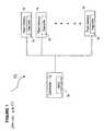
- FIG. 1A prior art flash memory system architecture 10 is shown in FIG. 1 , in relation to the basic architecture of the Nomura and the Yamagami patents.
- System 10includes a flash controller 12 operative to control flash memory devices 14 .
- Flash controller 12employs a memory resource (such as SRAM 16 ) for temporarily storing code and/or data that flash controller 12 uses when executing operations in its CPU.
- Each flash memory device 14includes a page buffer 18 for storing page data prior to programming the page data content to the non-volatile section of the flash memory.
- the present inventiondiscloses an improved and efficient system and method for utilizing an area of memory for temporary storage on a page buffer of the flash memory device itself, rather than on the flash controller.
- the proposed flash memory systemin accordance with a preferred embodiment of the present invention, includes a flash controller for controlling operation of at least two flash memory devices.
- a page bufferis allocated within each flash memory device, such that a first page buffer functions as a designated target buffer and a second page buffer functions as a mirror buffer.
- Temporary dataare transmitted to the two flash memory devices, preferably simultaneously. Therefore, the implementation of the proposed method does not require using the flash controller memory to back up page data until page programming to the non-volatile memory of the designated flash memory device is completed successfully.
- the area designated for temporary storage on the flash controllercan be completely removed or allocated for other purposes.
- a flash memory systemincluding: (a) at least two flash memory devices, wherein at least one page buffer is allocated within each of the at least two flash memory devices; and (b) a controller for controlling a programming of data into a first flash memory device by steps including transmitting the data from the controller both to a page buffer of the first flash memory device and to a page buffer of a second flash memory device.
- control over the programmingmay be implemented in software, in hardware or in a combination of software and hardware.
- the controlleris operative to transmit the data substantially simultaneously to both the page buffers.
- the controlleris operative to transmit the data consecutively to the page buffers.
- the flash memory systemalso includes a mechanism for checking a programming failure of the programming of the data in the first flash memory device.
- the controlleris operative to program the data into the second flash memory device in case of the programming failure in the first flash memory device.
- the controlleris operative, subsequent to the programming of the data into the second flash memory device, to read the data from the second flash memory device.
- the flash memory devicesare NAND flash memory devices.
- a method for managing a flash memory systemincluding the steps of, upon the flash memory system receiving an instruction from a host to store data, obeying the instruction by: (a) transmitting data to a first page buffer allocated within a first flash memory device of the flash memory system; and (b) also transmitting the data to a second page buffer allocated within a second flash memory device of the flash memory system.
- the dataare programmed to a non-volatile memory of the first flash memory device. More preferably, the programming of the data to the non-volatile memory of the first flash memory device is checked for failure. Still more preferably, if the checking indicates that the programming of the data to the non-volatile memory of the first flash memory device has failed, the data are programmed to a non-volatile memory of the second flash memory device. Most preferably, subsequent to the programming of the data into the non-volatile memory of the second flash memory device, the data are read from the non-volatile memory of the second flash memory device.
- dataare transmitted substantially simultaneously to both the page buffers.
- dataare transmitted consecutively to both the page buffers.
- FIG. 1is a block diagram of a prior art flash memory system architecture
- FIG. 2is a block diagram of a preferred embodiment of the flash memory system of the present invention.
- FIG. 3is a flow chart of a preferred embodiment of the method of the present invention.
- the present inventionis a system and method for utilizing an area of memory for temporary storage on a page buffer of the flash memory device itself, rather than on the flash controller.
- a preferred embodiment of the flash memory system of the present inventionincludes a flash controller for controlling operation of at least two flash memory devices.
- a page bufferis allocated within each flash memory device, such that a first page buffer functions as a designated target buffer and a second functions as a mirror buffer.
- the flash controllercontrols the transmission of data from the flash controller to the two page buffers and the programming of data from the designated target buffer to the non-volatile memory of the required flash memory device.
- a mechanism for checking a programming failure to the designated target bufferis further provided.
- the page datais not lost, since a copy of the original page data is available and ready in the mirror page buffer.
- Such a mechanismmay be embedded within the flash controller.
- the proposed methodis implemented in firmware and/or hardware.
- the present inventionovercomes the limitations caused when utilizing the flash controller memory for temporary storage. Firstly, there is no performance penalty, because the implementation of the present invention does not require using the flash controller memory to back up page data until page programming is completed successfully. Therefore, there is no delay in writing the next data page from the host computer to the flash controller. Additionally, the transmission of data to the two flash memory devices is carried out simultaneously, and therefore no time penalty is incurred.
- flash memory devicefor which the present invention is applicable is Samsung Electronics device No. K9K2GO8U0A.
- the datasheet of that flash memory deviceis incorporated by reference for all purposes as if fully set forth herein.
- the present inventionis not limited to this specific flash memory device. It should be understood that the present invention is not limited to one designated set of target/mirror buffers. Other implementations are possible within the scope of the invention, thus relating to a plurality of flash memory devices of any type containing a plurality of page buffers.
- System 20includes a flash controller 26 connected to two flash memory devices 22 and 24 , wherein each flash memory device ( 22 , 24 ) contains a page buffer ( 23 , 25 respectively).
- Flash controller 26is provided to control the programming of page data to a designated flash memory device while using a mirror buffer as a backup for programming failure events. For example, if the page data is defined to be programmed to flash memory device 22 , then page buffer 23 functions as the designated target buffer, while the backup data is stored in the page buffer 25 of flash memory device 24 functioning as the mirror buffer, and vise-versa. The functionality of flash buffers 23 and 25 is alternately swapped, according to the operation carried out by the flash controller 26 hardware signals 40 , 42 , 44 and 46 .
- flash controller 26asserts Chip Select (CS) signals 40 , 42 in order to activate the required flash memory device(s).
- CSChip Select
- both CS signals 40 , 42are asserted, the two flash memory devices 22 , 24 are activated simultaneously.
- FIG. 3there is shown a flow chart of a preferred method of the present invention.
- the command type(e.g. a write command) is defined along with the designated flash memory device to which page data should be written. Consequently, the page buffer functioning as the designated target buffer (to which the page data will be written) (e.g. page buffer 23 ) and the page buffer functioning as the mirror buffer (to which the backup data will be written) (e.g. page buffer 25 ) are also known.
- the page buffer functioning as the designated target buffer (to which the page data will be written)e.g. page buffer 23
- the page buffer functioning as the mirror bufferto which the backup data will be written
- page buffer 25e.g. page buffer 25
- both CS signalsare asserted, thus activating the two flash memory devices 22 and 24 simultaneously.
- the flash controller 26sends a command code for initiating a programming operation while defining the page address within the designated flash memory device (i.e. into which the programming operation should store the data).
- both flash memory devicesare set up to accept page data to be programmed.
- the Data phase 54again both CS signals ( 40 , 42 ) of flash controller 26 (see FIG. 2 ) are asserted, thus activating the two flash memory devices ( 24 , 22 respectively).
- flash controller 26transmits the page data to both flash memory devices simultaneously via data bus 44 .
- the two page buffers ( 23 , 25 ) on both flash memory devices ( 22 , 24 respectively)contain the same page data ready to be programmed.
- the Programming phase 56the flash memory device containing the designated target buffer is issued a ‘program’ command and programs the page data to its non-volatile area.
- the CS signal of this flash memory deviceis asserted, allowing only the designated flash memory device to be programmed.
- the flash controller 26reads the operation status transmitted via control bus 46 in order to verify that the programming operation to the designated flash memory device was successful, and that no write failure has occurred. During this phase, only the CS signal of the flash memory device containing the designated target buffer is asserted.
- step 60it is determined by the flash controller 26 whether a programming failure event has occurred.
- step 62the data page is not lost, because a copy of the original data page (i.e. backup page data) is available and ready in the mirror page buffer.
- the CS signal of the flash memory device containing the mirror bufferis asserted, followed by re-activation of steps 56 to 64 (wherein the mirror buffer functions as the designated target buffer). This results in the page data being programmed into the non-volatile memory of the flash memory device containing the mirror buffer, from which place it can be read by the controller and written again into a desirable location.
- the above methodresults in programming the page data into the flash memory device containing the mirror buffer at exactly the same address defined for programming into the flash memory device containing the target buffer. This may be undesirable, as that address might already be in use for existing data in the flash memory device containing the mirror buffer.
- the two flash memory devicesare set to different addresses—the flash memory device containing the designated target buffer is set to program the data into a desired address, while the flash memory device containing the mirror buffer is set to program the data into a preset address that is pre-selected by the controller to be available for use for such an error recovery purpose.
- Defining two separate addressesrequires modifying Setup phase 52 accordingly, such that in a first phase—a first CS signal is asserted for activating the flash memory device containing the designated target buffer only and providing the desired address. Whereas in a second phase—a second CS signal is asserted for activating the flash memory device containing the mirror buffer and providing the pre-selected address for programming the backed-up data in case of programming failure.
- step 64flash controller 26 continues to operate according to the current application, and no use is made of the backup copy of the data residing in the mirror buffer. However, no performance penalty was incurred, since as stated above—the transmission of the page data to the mirror buffer is achieved in parallel to the transmission of the page data to the designated target buffer and did not require an additional transmission procedure.
- the proposed flash memory systemuses Chip Select (CS) signals for activating the required flash memory device(s).
- CSChip Select
- activation of the required flash memory device(s) and selection of which of the flash memory device(s) will respond to a specific command or addresscan be further obtained using other approaches known in the art, such as by using Write Enable (WE) signals.
- WEWrite Enable
- the proposed methodmay also be executed by programming the page data to both flash memory devices (both the one containing the designated target buffer and the one containing the mirror buffer) in parallel.
- the backed-up data pagedoes not reside on the page buffer, but actually on the non-volatile section of the memory device containing the mirror buffer.
- implementing such a methodwould decrease the lifetime of this flash memory device, and so is not recommended.
- the present inventionis described herein as implemented using a NAND flash memory device. However, it can be understood that other implementations are possible within the scope of the invention, thus relating to any system and method utilizing an area of memory for temporary storage on the flash memory device itself, rather than on the flash controller.
Landscapes
- Engineering & Computer Science (AREA)
- Computer Hardware Design (AREA)
- Techniques For Improving Reliability Of Storages (AREA)
- Read Only Memory (AREA)
Abstract
Description
Claims (10)
Priority Applications (1)
| Application Number | Priority Date | Filing Date | Title |
|---|---|---|---|
| US11/318,863US8041879B2 (en) | 2005-02-18 | 2005-12-28 | Flash memory backup system and method |
Applications Claiming Priority (2)
| Application Number | Priority Date | Filing Date | Title |
|---|---|---|---|
| US65397605P | 2005-02-18 | 2005-02-18 | |
| US11/318,863US8041879B2 (en) | 2005-02-18 | 2005-12-28 | Flash memory backup system and method |
Publications (2)
| Publication Number | Publication Date |
|---|---|
| US20060198202A1 US20060198202A1 (en) | 2006-09-07 |
| US8041879B2true US8041879B2 (en) | 2011-10-18 |
Family
ID=36943977
Family Applications (1)
| Application Number | Title | Priority Date | Filing Date |
|---|---|---|---|
| US11/318,863Active2027-02-20US8041879B2 (en) | 2005-02-18 | 2005-12-28 | Flash memory backup system and method |
Country Status (1)
| Country | Link |
|---|---|
| US (1) | US8041879B2 (en) |
Cited By (37)
| Publication number | Priority date | Publication date | Assignee | Title |
|---|---|---|---|---|
| US20090187700A1 (en)* | 2008-01-18 | 2009-07-23 | Spansion Llc | Retargeting of a write operation retry in the event of a write operation failure |
| US20120004011A1 (en)* | 2010-07-01 | 2012-01-05 | Qualcomm Incorporated | Parallel Use of Integrated Non-Volatile Memory and Main Volatile Memory within a Mobile Device |
| US20120137093A1 (en)* | 2010-11-30 | 2012-05-31 | Micron Technology, Inc. | Reliable write for non-volatile memory |
| US20140298078A1 (en)* | 2013-04-01 | 2014-10-02 | Netapp, Inc. | SYNCHRONOUS MIRRORING OF NVLog TO MULTIPLE DESTINATIONS (ARCHITECTURE LEVEL) |
| US9377960B2 (en) | 2009-07-29 | 2016-06-28 | Hgst Technologies Santa Ana, Inc. | System and method of using stripes for recovering data in a flash storage system |
| US10347314B2 (en) | 2015-08-14 | 2019-07-09 | Spin Memory, Inc. | Method and apparatus for bipolar memory write-verify |
| US10360964B2 (en) | 2016-09-27 | 2019-07-23 | Spin Memory, Inc. | Method of writing contents in memory during a power up sequence using a dynamic redundancy register in a memory device |
| US10360962B1 (en) | 2017-12-28 | 2019-07-23 | Spin Memory, Inc. | Memory array with individually trimmable sense amplifiers |
| US10366774B2 (en) | 2016-09-27 | 2019-07-30 | Spin Memory, Inc. | Device with dynamic redundancy registers |
| US10395712B2 (en) | 2017-12-28 | 2019-08-27 | Spin Memory, Inc. | Memory array with horizontal source line and sacrificial bitline per virtual source |
| US10395711B2 (en) | 2017-12-28 | 2019-08-27 | Spin Memory, Inc. | Perpendicular source and bit lines for an MRAM array |
| US10437723B2 (en) | 2016-09-27 | 2019-10-08 | Spin Memory, Inc. | Method of flushing the contents of a dynamic redundancy register to a secure storage area during a power down in a memory device |
| US10437491B2 (en) | 2016-09-27 | 2019-10-08 | Spin Memory, Inc. | Method of processing incomplete memory operations in a memory device during a power up sequence and a power down sequence using a dynamic redundancy register |
| US10446744B2 (en) | 2018-03-08 | 2019-10-15 | Spin Memory, Inc. | Magnetic tunnel junction wafer adaptor used in magnetic annealing furnace and method of using the same |
| US10481976B2 (en) | 2017-10-24 | 2019-11-19 | Spin Memory, Inc. | Forcing bits as bad to widen the window between the distributions of acceptable high and low resistive bits thereby lowering the margin and increasing the speed of the sense amplifiers |
| US10489245B2 (en) | 2017-10-24 | 2019-11-26 | Spin Memory, Inc. | Forcing stuck bits, waterfall bits, shunt bits and low TMR bits to short during testing and using on-the-fly bit failure detection and bit redundancy remapping techniques to correct them |
| US10529915B2 (en) | 2018-03-23 | 2020-01-07 | Spin Memory, Inc. | Bit line structures for three-dimensional arrays with magnetic tunnel junction devices including an annular free magnetic layer and a planar reference magnetic layer |
| US10529439B2 (en) | 2017-10-24 | 2020-01-07 | Spin Memory, Inc. | On-the-fly bit failure detection and bit redundancy remapping techniques to correct for fixed bit defects |
| US10546625B2 (en) | 2016-09-27 | 2020-01-28 | Spin Memory, Inc. | Method of optimizing write voltage based on error buffer occupancy |
| US10546624B2 (en) | 2017-12-29 | 2020-01-28 | Spin Memory, Inc. | Multi-port random access memory |
| US10593396B2 (en) | 2018-07-06 | 2020-03-17 | Spin Memory, Inc. | Multi-bit cell read-out techniques for MRAM cells with mixed pinned magnetization orientations |
| US10600478B2 (en) | 2018-07-06 | 2020-03-24 | Spin Memory, Inc. | Multi-bit cell read-out techniques for MRAM cells with mixed pinned magnetization orientations |
| US10615337B2 (en) | 2018-05-30 | 2020-04-07 | Spin Memory, Inc. | Process for creating a high density magnetic tunnel junction array test platform |
| US10650875B2 (en) | 2018-08-21 | 2020-05-12 | Spin Memory, Inc. | System for a wide temperature range nonvolatile memory |
| US10656994B2 (en) | 2017-10-24 | 2020-05-19 | Spin Memory, Inc. | Over-voltage write operation of tunnel magnet-resistance (“TMR”) memory device and correcting failure bits therefrom by using on-the-fly bit failure detection and bit redundancy remapping techniques |
| US10784437B2 (en) | 2018-03-23 | 2020-09-22 | Spin Memory, Inc. | Three-dimensional arrays with MTJ devices including a free magnetic trench layer and a planar reference magnetic layer |
| US10811594B2 (en) | 2017-12-28 | 2020-10-20 | Spin Memory, Inc. | Process for hard mask development for MRAM pillar formation using photolithography |
| US10818331B2 (en) | 2016-09-27 | 2020-10-27 | Spin Memory, Inc. | Multi-chip module for MRAM devices with levels of dynamic redundancy registers |
| US10840439B2 (en) | 2017-12-29 | 2020-11-17 | Spin Memory, Inc. | Magnetic tunnel junction (MTJ) fabrication methods and systems |
| US10886330B2 (en) | 2017-12-29 | 2021-01-05 | Spin Memory, Inc. | Memory device having overlapping magnetic tunnel junctions in compliance with a reference pitch |
| US10891997B2 (en) | 2017-12-28 | 2021-01-12 | Spin Memory, Inc. | Memory array with horizontal source line and a virtual source line |
| US10971680B2 (en) | 2018-10-01 | 2021-04-06 | Spin Memory, Inc. | Multi terminal device stack formation methods |
| US11055011B2 (en) | 2019-08-07 | 2021-07-06 | Samsung Electronics Co., Ltd. | Storage device |
| US11107979B2 (en) | 2018-12-28 | 2021-08-31 | Spin Memory, Inc. | Patterned silicide structures and methods of manufacture |
| US11107974B2 (en) | 2018-03-23 | 2021-08-31 | Spin Memory, Inc. | Magnetic tunnel junction devices including a free magnetic trench layer and a planar reference magnetic layer |
| US11107978B2 (en) | 2018-03-23 | 2021-08-31 | Spin Memory, Inc. | Methods of manufacturing three-dimensional arrays with MTJ devices including a free magnetic trench layer and a planar reference magnetic layer |
| US11621293B2 (en) | 2018-10-01 | 2023-04-04 | Integrated Silicon Solution, (Cayman) Inc. | Multi terminal device stack systems and methods |
Families Citing this family (57)
| Publication number | Priority date | Publication date | Assignee | Title |
|---|---|---|---|---|
| US7676231B2 (en)* | 2005-04-13 | 2010-03-09 | Intel Corporation | Methods and apparatus for selecting communication channels based on channel load information |
| US11948629B2 (en) | 2005-09-30 | 2024-04-02 | Mosaid Technologies Incorporated | Non-volatile memory device with concurrent bank operations |
| US7652922B2 (en) | 2005-09-30 | 2010-01-26 | Mosaid Technologies Incorporated | Multiple independent serial link memory |
| KR101293365B1 (en)* | 2005-09-30 | 2013-08-05 | 모사이드 테크놀로지스 인코퍼레이티드 | Memory with output control |
| US7747833B2 (en) | 2005-09-30 | 2010-06-29 | Mosaid Technologies Incorporated | Independent link and bank selection |
| US20070076502A1 (en) | 2005-09-30 | 2007-04-05 | Pyeon Hong B | Daisy chain cascading devices |
| TWI460736B (en)* | 2005-09-30 | 2014-11-11 | Conversant Intellectual Property Man Inc | Independent link and bank selection |
| US8195444B2 (en) | 2005-10-12 | 2012-06-05 | Storage Appliance Corporation | Systems and methods for automated diagnosis and repair of storage devices |
| US8069271B2 (en)* | 2005-10-12 | 2011-11-29 | Storage Appliance Corporation | Systems and methods for converting a media player into a backup device |
| US7844445B2 (en) | 2005-10-12 | 2010-11-30 | Storage Appliance Corporation | Automatic connection to an online service provider from a backup system |
| US7899662B2 (en)* | 2005-10-12 | 2011-03-01 | Storage Appliance Corporation | Data backup system including a data protection component |
| US7813913B2 (en)* | 2005-10-12 | 2010-10-12 | Storage Appliance Corporation | Emulation component for data backup applications |
| US7818160B2 (en)* | 2005-10-12 | 2010-10-19 | Storage Appliance Corporation | Data backup devices and methods for backing up data |
| US20070162271A1 (en)* | 2005-10-12 | 2007-07-12 | Storage Appliance Corporation | Systems and methods for selecting and printing data files from a backup system |
| US7702830B2 (en)* | 2005-10-12 | 2010-04-20 | Storage Appliance Corporation | Methods for selectively copying data files to networked storage and devices for initiating the same |
| US7822595B2 (en) | 2005-10-12 | 2010-10-26 | Storage Appliance Corporation | Systems and methods for selectively copying embedded data files |
| US7904639B2 (en) | 2006-08-22 | 2011-03-08 | Mosaid Technologies Incorporated | Modular command structure for memory and memory system |
| US20080126446A1 (en)* | 2006-11-27 | 2008-05-29 | Storage Appliance Corporation | Systems and methods for backing up user settings |
| KR100877610B1 (en)* | 2007-01-23 | 2009-01-09 | 삼성전자주식회사 | Page data storage method and storage device |
| US8086785B2 (en)* | 2007-02-22 | 2011-12-27 | Mosaid Technologies Incorporated | System and method of page buffer operation for memory devices |
| WO2008101316A1 (en)* | 2007-02-22 | 2008-08-28 | Mosaid Technologies Incorporated | Apparatus and method for using a page buffer of a memory device as a temporary cache |
| KR100823175B1 (en)* | 2007-02-27 | 2008-04-18 | 삼성전자주식회사 | Flash memory devices and memory systems containing them that can improve program performance |
| US20080226082A1 (en)* | 2007-03-12 | 2008-09-18 | Storage Appliance Corporation | Systems and methods for secure data backup |
| US20090031298A1 (en)* | 2007-06-11 | 2009-01-29 | Jeffrey Brunet | System and method for automated installation and/or launch of software |
| US20090030955A1 (en)* | 2007-06-11 | 2009-01-29 | Storage Appliance Corporation | Automated data backup with graceful shutdown for vista-based system |
| US8527690B2 (en)* | 2008-06-26 | 2013-09-03 | Microsoft Corporation | Optimization of non-volatile solid-state memory by moving data based on data generation and memory wear |
| US8139390B2 (en)* | 2008-07-08 | 2012-03-20 | Mosaid Technologies Incorporated | Mixed data rates in memory devices and systems |
| US8161313B2 (en)* | 2008-09-30 | 2012-04-17 | Mosaid Technologies Incorporated | Serial-connected memory system with duty cycle correction |
| US8181056B2 (en)* | 2008-09-30 | 2012-05-15 | Mosaid Technologies Incorporated | Serial-connected memory system with output delay adjustment |
| TWI419165B (en)* | 2009-02-23 | 2013-12-11 | System and method for memory management and dynamic data backup | |
| US8832353B2 (en)* | 2009-04-07 | 2014-09-09 | Sandisk Technologies Inc. | Host stop-transmission handling |
| TWI417893B (en)* | 2009-05-06 | 2013-12-01 | Silicon Motion Inc | Data accessing apparatus and data accessing method |
| TWI416523B (en)* | 2009-06-10 | 2013-11-21 | Silicon Motion Inc | Method for writing fail retry for a non-volatile memory, non-volatile memory, controller, and memory card |
| US8307241B2 (en)* | 2009-06-16 | 2012-11-06 | Sandisk Technologies Inc. | Data recovery in multi-level cell nonvolatile memory |
| US8132045B2 (en)* | 2009-06-16 | 2012-03-06 | SanDisk Technologies, Inc. | Program failure handling in nonvolatile memory |
| EP2270662A1 (en)* | 2009-06-29 | 2011-01-05 | Thomson Licensing | Method and apparatus for dealing with write errors when writing information data into flash memory devices |
| US8413137B2 (en) | 2010-02-04 | 2013-04-02 | Storage Appliance Corporation | Automated network backup peripheral device and method |
| US9836370B2 (en) | 2010-11-18 | 2017-12-05 | Lenovo Enterprise Solutions (Singapore) Pte. Ltd. | Backup memory administration using an active memory device and a backup memory device |
| JP2013069171A (en)* | 2011-09-22 | 2013-04-18 | Toshiba Corp | Memory system and control method thereof |
| JP2013229086A (en)* | 2012-04-27 | 2013-11-07 | Sony Corp | Memory device, memory control device, and memory control method |
| US9037902B2 (en) | 2013-03-15 | 2015-05-19 | Sandisk Technologies Inc. | Flash memory techniques for recovering from write interrupt resulting from voltage fault |
| US9952784B2 (en)* | 2015-03-11 | 2018-04-24 | Sandisk Technologies Llc | Multichip dual write |
| US10115446B1 (en)* | 2015-04-21 | 2018-10-30 | Spin Transfer Technologies, Inc. | Spin transfer torque MRAM device with error buffer |
| US9507663B1 (en)* | 2015-05-04 | 2016-11-29 | Macronix International Co., Ltd. | Memory device and operation method |
| US10460781B2 (en) | 2016-09-27 | 2019-10-29 | Spin Memory, Inc. | Memory device with a dual Y-multiplexer structure for performing two simultaneous operations on the same row of a memory bank |
| US10446210B2 (en) | 2016-09-27 | 2019-10-15 | Spin Memory, Inc. | Memory instruction pipeline with a pre-read stage for a write operation for reducing power consumption in a memory device that uses dynamic redundancy registers |
| KR20190063054A (en)* | 2017-11-29 | 2019-06-07 | 삼성전자주식회사 | Memory System and Operation Method thereof |
| US10424726B2 (en) | 2017-12-28 | 2019-09-24 | Spin Memory, Inc. | Process for improving photoresist pillar adhesion during MRAM fabrication |
| US10784439B2 (en) | 2017-12-29 | 2020-09-22 | Spin Memory, Inc. | Precessional spin current magnetic tunnel junction devices and methods of manufacture |
| US10840436B2 (en) | 2017-12-29 | 2020-11-17 | Spin Memory, Inc. | Perpendicular magnetic anisotropy interface tunnel junction devices and methods of manufacture |
| US10367139B2 (en) | 2017-12-29 | 2019-07-30 | Spin Memory, Inc. | Methods of manufacturing magnetic tunnel junction devices |
| US10424723B2 (en) | 2017-12-29 | 2019-09-24 | Spin Memory, Inc. | Magnetic tunnel junction devices including an optimization layer |
| US10438995B2 (en) | 2018-01-08 | 2019-10-08 | Spin Memory, Inc. | Devices including magnetic tunnel junctions integrated with selectors |
| US10438996B2 (en) | 2018-01-08 | 2019-10-08 | Spin Memory, Inc. | Methods of fabricating magnetic tunnel junctions integrated with selectors |
| US10692569B2 (en) | 2018-07-06 | 2020-06-23 | Spin Memory, Inc. | Read-out techniques for multi-bit cells |
| US10559338B2 (en) | 2018-07-06 | 2020-02-11 | Spin Memory, Inc. | Multi-bit cell read-out techniques |
| US10699761B2 (en) | 2018-09-18 | 2020-06-30 | Spin Memory, Inc. | Word line decoder memory architecture |
Citations (11)
| Publication number | Priority date | Publication date | Assignee | Title |
|---|---|---|---|---|
| US5426774A (en)* | 1993-04-06 | 1995-06-20 | Honeywell Inc. | Method for maintaining a sequence of events function during failover in a redundant multiple layer system |
| US5887270A (en)* | 1995-11-21 | 1999-03-23 | Emc Corporation | Fault tolerant controller system and method |
| US6038680A (en)* | 1996-12-11 | 2000-03-14 | Compaq Computer Corporation | Failover memory for a computer system |
| US6338126B1 (en)* | 1999-12-06 | 2002-01-08 | Legato Systems, Inc. | Crash recovery without complete remirror |
| US20020026566A1 (en)* | 1998-06-08 | 2002-02-28 | Kosaku Awada | Data backup in non-volatile memory |
| US6601132B2 (en) | 2000-09-29 | 2003-07-29 | Kabushiki Kaisha Toshiba | Nonvolatile memory and method of writing data thereto |
| US6788609B2 (en) | 1991-11-26 | 2004-09-07 | Renesas Technology Corp. | Storage device employing a flash memory |
| US7634507B2 (en)* | 2006-08-30 | 2009-12-15 | Inmage Systems, Inc. | Ensuring data persistence and consistency in enterprise storage backup systems |
| US7774537B2 (en)* | 2007-02-22 | 2010-08-10 | Mosaid Technologies Incorporated | Apparatus and method of page program operation for memory devices with mirror back-up of data |
| US20100287433A1 (en)* | 2009-05-06 | 2010-11-11 | Chung-Su Mu | Data access apparatus and data access method |
| US20110002165A1 (en)* | 2009-07-02 | 2011-01-06 | Kabushiki Kaisha Toshiba | Flash memory |
- 2005
- 2005-12-28USUS11/318,863patent/US8041879B2/enactiveActive
Patent Citations (11)
| Publication number | Priority date | Publication date | Assignee | Title |
|---|---|---|---|---|
| US6788609B2 (en) | 1991-11-26 | 2004-09-07 | Renesas Technology Corp. | Storage device employing a flash memory |
| US5426774A (en)* | 1993-04-06 | 1995-06-20 | Honeywell Inc. | Method for maintaining a sequence of events function during failover in a redundant multiple layer system |
| US5887270A (en)* | 1995-11-21 | 1999-03-23 | Emc Corporation | Fault tolerant controller system and method |
| US6038680A (en)* | 1996-12-11 | 2000-03-14 | Compaq Computer Corporation | Failover memory for a computer system |
| US20020026566A1 (en)* | 1998-06-08 | 2002-02-28 | Kosaku Awada | Data backup in non-volatile memory |
| US6338126B1 (en)* | 1999-12-06 | 2002-01-08 | Legato Systems, Inc. | Crash recovery without complete remirror |
| US6601132B2 (en) | 2000-09-29 | 2003-07-29 | Kabushiki Kaisha Toshiba | Nonvolatile memory and method of writing data thereto |
| US7634507B2 (en)* | 2006-08-30 | 2009-12-15 | Inmage Systems, Inc. | Ensuring data persistence and consistency in enterprise storage backup systems |
| US7774537B2 (en)* | 2007-02-22 | 2010-08-10 | Mosaid Technologies Incorporated | Apparatus and method of page program operation for memory devices with mirror back-up of data |
| US20100287433A1 (en)* | 2009-05-06 | 2010-11-11 | Chung-Su Mu | Data access apparatus and data access method |
| US20110002165A1 (en)* | 2009-07-02 | 2011-01-06 | Kabushiki Kaisha Toshiba | Flash memory |
Non-Patent Citations (2)
| Title |
|---|
| PC Guide. RAID level 1. Archive.org date of Feb. 11, 2001. http://www.pcguide.com/ref/hdd/perf/raid/levels/singleLevel1-c.html.* |
| Tanenbaum, A. S. Structured Computer Organization. 1984. Prentice Hall Inc. 2nd ed. pp. 10-12.* |
Cited By (43)
| Publication number | Priority date | Publication date | Assignee | Title |
|---|---|---|---|---|
| US8694714B2 (en)* | 2008-01-18 | 2014-04-08 | Spansion Llc | Retargeting of a write operation retry in the event of a write operation failure |
| US20090187700A1 (en)* | 2008-01-18 | 2009-07-23 | Spansion Llc | Retargeting of a write operation retry in the event of a write operation failure |
| US9377960B2 (en) | 2009-07-29 | 2016-06-28 | Hgst Technologies Santa Ana, Inc. | System and method of using stripes for recovering data in a flash storage system |
| US20120004011A1 (en)* | 2010-07-01 | 2012-01-05 | Qualcomm Incorporated | Parallel Use of Integrated Non-Volatile Memory and Main Volatile Memory within a Mobile Device |
| US10360143B2 (en)* | 2010-07-01 | 2019-07-23 | Qualcomm Incorporated | Parallel use of integrated non-volatile memory and main volatile memory within a mobile device |
| US20120137093A1 (en)* | 2010-11-30 | 2012-05-31 | Micron Technology, Inc. | Reliable write for non-volatile memory |
| US9307011B2 (en)* | 2013-04-01 | 2016-04-05 | Netapp, Inc. | Synchronous mirroring of NVLog to multiple destinations (architecture level) |
| US20140298078A1 (en)* | 2013-04-01 | 2014-10-02 | Netapp, Inc. | SYNCHRONOUS MIRRORING OF NVLog TO MULTIPLE DESTINATIONS (ARCHITECTURE LEVEL) |
| US10347314B2 (en) | 2015-08-14 | 2019-07-09 | Spin Memory, Inc. | Method and apparatus for bipolar memory write-verify |
| US10818331B2 (en) | 2016-09-27 | 2020-10-27 | Spin Memory, Inc. | Multi-chip module for MRAM devices with levels of dynamic redundancy registers |
| US10366774B2 (en) | 2016-09-27 | 2019-07-30 | Spin Memory, Inc. | Device with dynamic redundancy registers |
| US10366775B2 (en) | 2016-09-27 | 2019-07-30 | Spin Memory, Inc. | Memory device using levels of dynamic redundancy registers for writing a data word that failed a write operation |
| US10360964B2 (en) | 2016-09-27 | 2019-07-23 | Spin Memory, Inc. | Method of writing contents in memory during a power up sequence using a dynamic redundancy register in a memory device |
| US10424393B2 (en) | 2016-09-27 | 2019-09-24 | Spin Memory, Inc. | Method of reading data from a memory device using multiple levels of dynamic redundancy registers |
| US10437723B2 (en) | 2016-09-27 | 2019-10-08 | Spin Memory, Inc. | Method of flushing the contents of a dynamic redundancy register to a secure storage area during a power down in a memory device |
| US10437491B2 (en) | 2016-09-27 | 2019-10-08 | Spin Memory, Inc. | Method of processing incomplete memory operations in a memory device during a power up sequence and a power down sequence using a dynamic redundancy register |
| US10546625B2 (en) | 2016-09-27 | 2020-01-28 | Spin Memory, Inc. | Method of optimizing write voltage based on error buffer occupancy |
| US10529439B2 (en) | 2017-10-24 | 2020-01-07 | Spin Memory, Inc. | On-the-fly bit failure detection and bit redundancy remapping techniques to correct for fixed bit defects |
| US10656994B2 (en) | 2017-10-24 | 2020-05-19 | Spin Memory, Inc. | Over-voltage write operation of tunnel magnet-resistance (“TMR”) memory device and correcting failure bits therefrom by using on-the-fly bit failure detection and bit redundancy remapping techniques |
| US10481976B2 (en) | 2017-10-24 | 2019-11-19 | Spin Memory, Inc. | Forcing bits as bad to widen the window between the distributions of acceptable high and low resistive bits thereby lowering the margin and increasing the speed of the sense amplifiers |
| US10489245B2 (en) | 2017-10-24 | 2019-11-26 | Spin Memory, Inc. | Forcing stuck bits, waterfall bits, shunt bits and low TMR bits to short during testing and using on-the-fly bit failure detection and bit redundancy remapping techniques to correct them |
| US10360962B1 (en) | 2017-12-28 | 2019-07-23 | Spin Memory, Inc. | Memory array with individually trimmable sense amplifiers |
| US10811594B2 (en) | 2017-12-28 | 2020-10-20 | Spin Memory, Inc. | Process for hard mask development for MRAM pillar formation using photolithography |
| US10395712B2 (en) | 2017-12-28 | 2019-08-27 | Spin Memory, Inc. | Memory array with horizontal source line and sacrificial bitline per virtual source |
| US10891997B2 (en) | 2017-12-28 | 2021-01-12 | Spin Memory, Inc. | Memory array with horizontal source line and a virtual source line |
| US10395711B2 (en) | 2017-12-28 | 2019-08-27 | Spin Memory, Inc. | Perpendicular source and bit lines for an MRAM array |
| US10930332B2 (en) | 2017-12-28 | 2021-02-23 | Spin Memory, Inc. | Memory array with individually trimmable sense amplifiers |
| US10546624B2 (en) | 2017-12-29 | 2020-01-28 | Spin Memory, Inc. | Multi-port random access memory |
| US10840439B2 (en) | 2017-12-29 | 2020-11-17 | Spin Memory, Inc. | Magnetic tunnel junction (MTJ) fabrication methods and systems |
| US10886330B2 (en) | 2017-12-29 | 2021-01-05 | Spin Memory, Inc. | Memory device having overlapping magnetic tunnel junctions in compliance with a reference pitch |
| US10446744B2 (en) | 2018-03-08 | 2019-10-15 | Spin Memory, Inc. | Magnetic tunnel junction wafer adaptor used in magnetic annealing furnace and method of using the same |
| US10529915B2 (en) | 2018-03-23 | 2020-01-07 | Spin Memory, Inc. | Bit line structures for three-dimensional arrays with magnetic tunnel junction devices including an annular free magnetic layer and a planar reference magnetic layer |
| US11107974B2 (en) | 2018-03-23 | 2021-08-31 | Spin Memory, Inc. | Magnetic tunnel junction devices including a free magnetic trench layer and a planar reference magnetic layer |
| US11107978B2 (en) | 2018-03-23 | 2021-08-31 | Spin Memory, Inc. | Methods of manufacturing three-dimensional arrays with MTJ devices including a free magnetic trench layer and a planar reference magnetic layer |
| US10784437B2 (en) | 2018-03-23 | 2020-09-22 | Spin Memory, Inc. | Three-dimensional arrays with MTJ devices including a free magnetic trench layer and a planar reference magnetic layer |
| US10615337B2 (en) | 2018-05-30 | 2020-04-07 | Spin Memory, Inc. | Process for creating a high density magnetic tunnel junction array test platform |
| US10600478B2 (en) | 2018-07-06 | 2020-03-24 | Spin Memory, Inc. | Multi-bit cell read-out techniques for MRAM cells with mixed pinned magnetization orientations |
| US10593396B2 (en) | 2018-07-06 | 2020-03-17 | Spin Memory, Inc. | Multi-bit cell read-out techniques for MRAM cells with mixed pinned magnetization orientations |
| US10650875B2 (en) | 2018-08-21 | 2020-05-12 | Spin Memory, Inc. | System for a wide temperature range nonvolatile memory |
| US10971680B2 (en) | 2018-10-01 | 2021-04-06 | Spin Memory, Inc. | Multi terminal device stack formation methods |
| US11621293B2 (en) | 2018-10-01 | 2023-04-04 | Integrated Silicon Solution, (Cayman) Inc. | Multi terminal device stack systems and methods |
| US11107979B2 (en) | 2018-12-28 | 2021-08-31 | Spin Memory, Inc. | Patterned silicide structures and methods of manufacture |
| US11055011B2 (en) | 2019-08-07 | 2021-07-06 | Samsung Electronics Co., Ltd. | Storage device |
Also Published As
| Publication number | Publication date |
|---|---|
| US20060198202A1 (en) | 2006-09-07 |
Similar Documents
| Publication | Publication Date | Title |
|---|---|---|
| US8041879B2 (en) | Flash memory backup system and method | |
| KR101004876B1 (en) | Power Management Blocks for Use in Nonvolatile Memory Systems | |
| US7975119B2 (en) | Device for prioritized erasure of flash memory | |
| US7089349B2 (en) | Internal maintenance schedule request for non-volatile memory system | |
| EP1729304B1 (en) | Space management for managing high capacity nonvolatile memory | |
| JP4429685B2 (en) | Hybrid implementation for error correction code in non-volatile memory systems | |
| KR100622349B1 (en) | A method for managing a defective block in a flash memory device and a flash memory device having a defective block management function. | |
| US7174440B2 (en) | Method and apparatus for performing block caching in a non-volatile memory system | |
| US7702880B2 (en) | Hybrid mapping implementation within a non-volatile memory system | |
| KR100906519B1 (en) | Unusable block management within a non-volatile memory system | |
| US6034897A (en) | Space management for managing high capacity nonvolatile memory | |
| US8484409B2 (en) | Nonvolatile memory controller with logical defective cluster table | |
| US20110271041A1 (en) | Electronic device comprising flash memory and related method of handling program failures | |
| JP5486047B2 (en) | Device and method for prioritized erase of flash memory | |
| US20150186224A1 (en) | Data storage device and flash memory control method | |
| US20080037321A1 (en) | Partial-Write-Collector Algorithm for Multi Level Cell (MLC) Flash | |
| US8117414B2 (en) | Method for prioritized erasure of flash memory | |
| US8706990B2 (en) | Adaptive internal table backup for non-volatile memory system | |
| JPWO2009004674A1 (en) | Storage device, disk device, write determination method, control device | |
| JP3670151B2 (en) | Flash memory access method, system including driver for accessing flash memory, and flash memory | |
| JP2003263894A (en) | Control method for nonvolatile semiconductor memory device | |
| JP2003242788A (en) | Nonvolatile semiconductor memory device and control method thereof | |
| JP4421659B2 (en) | Electronic device having flash memory | |
| JP4090071B2 (en) | Flash EEprom system |
Legal Events
| Date | Code | Title | Description |
|---|---|---|---|
| AS | Assignment | Owner name:M-SYSTEMS FLASH DISK PIONEERS, LTD., ISRAEL Free format text:ASSIGNMENT OF ASSIGNORS INTEREST;ASSIGNOR:EREZ, ERAN;REEL/FRAME:017418/0216 Effective date:20051225 | |
| AS | Assignment | Owner name:MSYSTEMS LTD, ISRAEL Free format text:CHANGE OF NAME;ASSIGNOR:M-SYSTEMS FLASH DISK PIONEERS LTD.;REEL/FRAME:021798/0341 Effective date:20060504 | |
| AS | Assignment | Owner name:SANDISK IL LTD., ISRAEL Free format text:CHANGE OF NAME;ASSIGNOR:MSYSTEMS LTD;REEL/FRAME:021853/0793 Effective date:20070101 | |
| STCF | Information on status: patent grant | Free format text:PATENTED CASE | |
| FPAY | Fee payment | Year of fee payment:4 | |
| MAFP | Maintenance fee payment | Free format text:PAYMENT OF MAINTENANCE FEE, 8TH YEAR, LARGE ENTITY (ORIGINAL EVENT CODE: M1552); ENTITY STATUS OF PATENT OWNER: LARGE ENTITY Year of fee payment:8 | |
| AS | Assignment | Owner name:WESTERN DIGITAL ISRAEL LTD, ISRAEL Free format text:CHANGE OF NAME;ASSIGNOR:SANDISK IL LTD;REEL/FRAME:053574/0513 Effective date:20191112 | |
| MAFP | Maintenance fee payment | Free format text:PAYMENT OF MAINTENANCE FEE, 12TH YEAR, LARGE ENTITY (ORIGINAL EVENT CODE: M1553); ENTITY STATUS OF PATENT OWNER: LARGE ENTITY Year of fee payment:12 | |
| AS | Assignment | Owner name:SANDISK ISRAEL LTD., ISRAEL Free format text:CHANGE OF NAME;ASSIGNOR:WESTERN DIGITAL ISRAEL LTD.;REEL/FRAME:071587/0836 Effective date:20250409 |