US8039389B2 - Semiconductor device having an organic anti-reflective coating (ARC) and method therefor - Google Patents
Semiconductor device having an organic anti-reflective coating (ARC) and method thereforDownload PDFInfo
- Publication number
- US8039389B2 US8039389B2US11/676,100US67610007AUS8039389B2US 8039389 B2US8039389 B2US 8039389B2US 67610007 AUS67610007 AUS 67610007AUS 8039389 B2US8039389 B2US 8039389B2
- Authority
- US
- United States
- Prior art keywords
- layer
- arc
- teos
- photoresist
- organic
- Prior art date
- Legal status (The legal status is an assumption and is not a legal conclusion. Google has not performed a legal analysis and makes no representation as to the accuracy of the status listed.)
- Expired - Lifetime, expires
Links
Images


Classifications
- H—ELECTRICITY
- H01—ELECTRIC ELEMENTS
- H01L—SEMICONDUCTOR DEVICES NOT COVERED BY CLASS H10
- H01L21/00—Processes or apparatus adapted for the manufacture or treatment of semiconductor or solid state devices or of parts thereof
- H01L21/02—Manufacture or treatment of semiconductor devices or of parts thereof
- H01L21/04—Manufacture or treatment of semiconductor devices or of parts thereof the devices having potential barriers, e.g. a PN junction, depletion layer or carrier concentration layer
- H01L21/18—Manufacture or treatment of semiconductor devices or of parts thereof the devices having potential barriers, e.g. a PN junction, depletion layer or carrier concentration layer the devices having semiconductor bodies comprising elements of Group IV of the Periodic Table or AIIIBV compounds with or without impurities, e.g. doping materials
- H01L21/30—Treatment of semiconductor bodies using processes or apparatus not provided for in groups H01L21/20 - H01L21/26
- H01L21/31—Treatment of semiconductor bodies using processes or apparatus not provided for in groups H01L21/20 - H01L21/26 to form insulating layers thereon, e.g. for masking or by using photolithographic techniques; After treatment of these layers; Selection of materials for these layers
- H01L21/3205—Deposition of non-insulating-, e.g. conductive- or resistive-, layers on insulating layers; After-treatment of these layers
- H—ELECTRICITY
- H01—ELECTRIC ELEMENTS
- H01L—SEMICONDUCTOR DEVICES NOT COVERED BY CLASS H10
- H01L21/00—Processes or apparatus adapted for the manufacture or treatment of semiconductor or solid state devices or of parts thereof
- H01L21/02—Manufacture or treatment of semiconductor devices or of parts thereof
- H01L21/02104—Forming layers
- H01L21/02107—Forming insulating materials on a substrate
- H01L21/02109—Forming insulating materials on a substrate characterised by the type of layer, e.g. type of material, porous/non-porous, pre-cursors, mixtures or laminates
- H01L21/02112—Forming insulating materials on a substrate characterised by the type of layer, e.g. type of material, porous/non-porous, pre-cursors, mixtures or laminates characterised by the material of the layer
- H01L21/02123—Forming insulating materials on a substrate characterised by the type of layer, e.g. type of material, porous/non-porous, pre-cursors, mixtures or laminates characterised by the material of the layer the material containing silicon
- H01L21/02164—Forming insulating materials on a substrate characterised by the type of layer, e.g. type of material, porous/non-porous, pre-cursors, mixtures or laminates characterised by the material of the layer the material containing silicon the material being a silicon oxide, e.g. SiO2
- H—ELECTRICITY
- H01—ELECTRIC ELEMENTS
- H01L—SEMICONDUCTOR DEVICES NOT COVERED BY CLASS H10
- H01L21/00—Processes or apparatus adapted for the manufacture or treatment of semiconductor or solid state devices or of parts thereof
- H01L21/02—Manufacture or treatment of semiconductor devices or of parts thereof
- H01L21/02104—Forming layers
- H01L21/02107—Forming insulating materials on a substrate
- H01L21/02225—Forming insulating materials on a substrate characterised by the process for the formation of the insulating layer
- H01L21/0226—Forming insulating materials on a substrate characterised by the process for the formation of the insulating layer formation by a deposition process
- H01L21/02263—Forming insulating materials on a substrate characterised by the process for the formation of the insulating layer formation by a deposition process deposition from the gas or vapour phase
- H01L21/02271—Forming insulating materials on a substrate characterised by the process for the formation of the insulating layer formation by a deposition process deposition from the gas or vapour phase deposition by decomposition or reaction of gaseous or vapour phase compounds, i.e. chemical vapour deposition
- H01L21/02274—Forming insulating materials on a substrate characterised by the process for the formation of the insulating layer formation by a deposition process deposition from the gas or vapour phase deposition by decomposition or reaction of gaseous or vapour phase compounds, i.e. chemical vapour deposition in the presence of a plasma [PECVD]
- H—ELECTRICITY
- H01—ELECTRIC ELEMENTS
- H01L—SEMICONDUCTOR DEVICES NOT COVERED BY CLASS H10
- H01L21/00—Processes or apparatus adapted for the manufacture or treatment of semiconductor or solid state devices or of parts thereof
- H01L21/02—Manufacture or treatment of semiconductor devices or of parts thereof
- H01L21/027—Making masks on semiconductor bodies for further photolithographic processing not provided for in group H01L21/18 or H01L21/34
- H01L21/0271—Making masks on semiconductor bodies for further photolithographic processing not provided for in group H01L21/18 or H01L21/34 comprising organic layers
- H01L21/0273—Making masks on semiconductor bodies for further photolithographic processing not provided for in group H01L21/18 or H01L21/34 comprising organic layers characterised by the treatment of photoresist layers
- H01L21/0274—Photolithographic processes
- H01L21/0276—Photolithographic processes using an anti-reflective coating
- H—ELECTRICITY
- H01—ELECTRIC ELEMENTS
- H01L—SEMICONDUCTOR DEVICES NOT COVERED BY CLASS H10
- H01L21/00—Processes or apparatus adapted for the manufacture or treatment of semiconductor or solid state devices or of parts thereof
- H01L21/02—Manufacture or treatment of semiconductor devices or of parts thereof
- H01L21/027—Making masks on semiconductor bodies for further photolithographic processing not provided for in group H01L21/18 or H01L21/34
- H01L21/033—Making masks on semiconductor bodies for further photolithographic processing not provided for in group H01L21/18 or H01L21/34 comprising inorganic layers
- H01L21/0332—Making masks on semiconductor bodies for further photolithographic processing not provided for in group H01L21/18 or H01L21/34 comprising inorganic layers characterised by their composition, e.g. multilayer masks, materials
- H—ELECTRICITY
- H01—ELECTRIC ELEMENTS
- H01L—SEMICONDUCTOR DEVICES NOT COVERED BY CLASS H10
- H01L21/00—Processes or apparatus adapted for the manufacture or treatment of semiconductor or solid state devices or of parts thereof
- H01L21/02—Manufacture or treatment of semiconductor devices or of parts thereof
- H01L21/027—Making masks on semiconductor bodies for further photolithographic processing not provided for in group H01L21/18 or H01L21/34
- H01L21/033—Making masks on semiconductor bodies for further photolithographic processing not provided for in group H01L21/18 or H01L21/34 comprising inorganic layers
- H01L21/0334—Making masks on semiconductor bodies for further photolithographic processing not provided for in group H01L21/18 or H01L21/34 comprising inorganic layers characterised by their size, orientation, disposition, behaviour, shape, in horizontal or vertical plane
- H01L21/0338—Process specially adapted to improve the resolution of the mask
- H—ELECTRICITY
- H01—ELECTRIC ELEMENTS
- H01L—SEMICONDUCTOR DEVICES NOT COVERED BY CLASS H10
- H01L21/00—Processes or apparatus adapted for the manufacture or treatment of semiconductor or solid state devices or of parts thereof
- H01L21/02—Manufacture or treatment of semiconductor devices or of parts thereof
- H01L21/04—Manufacture or treatment of semiconductor devices or of parts thereof the devices having potential barriers, e.g. a PN junction, depletion layer or carrier concentration layer
- H01L21/18—Manufacture or treatment of semiconductor devices or of parts thereof the devices having potential barriers, e.g. a PN junction, depletion layer or carrier concentration layer the devices having semiconductor bodies comprising elements of Group IV of the Periodic Table or AIIIBV compounds with or without impurities, e.g. doping materials
- H01L21/28—Manufacture of electrodes on semiconductor bodies using processes or apparatus not provided for in groups H01L21/20 - H01L21/268
- H01L21/28008—Making conductor-insulator-semiconductor electrodes
- H01L21/28017—Making conductor-insulator-semiconductor electrodes the insulator being formed after the semiconductor body, the semiconductor being silicon
- H01L21/28026—Making conductor-insulator-semiconductor electrodes the insulator being formed after the semiconductor body, the semiconductor being silicon characterised by the conductor
- H01L21/28035—Making conductor-insulator-semiconductor electrodes the insulator being formed after the semiconductor body, the semiconductor being silicon characterised by the conductor the final conductor layer next to the insulator being silicon, e.g. polysilicon, with or without impurities
- H—ELECTRICITY
- H01—ELECTRIC ELEMENTS
- H01L—SEMICONDUCTOR DEVICES NOT COVERED BY CLASS H10
- H01L21/00—Processes or apparatus adapted for the manufacture or treatment of semiconductor or solid state devices or of parts thereof
- H01L21/02—Manufacture or treatment of semiconductor devices or of parts thereof
- H01L21/04—Manufacture or treatment of semiconductor devices or of parts thereof the devices having potential barriers, e.g. a PN junction, depletion layer or carrier concentration layer
- H01L21/18—Manufacture or treatment of semiconductor devices or of parts thereof the devices having potential barriers, e.g. a PN junction, depletion layer or carrier concentration layer the devices having semiconductor bodies comprising elements of Group IV of the Periodic Table or AIIIBV compounds with or without impurities, e.g. doping materials
- H01L21/28—Manufacture of electrodes on semiconductor bodies using processes or apparatus not provided for in groups H01L21/20 - H01L21/268
- H01L21/28008—Making conductor-insulator-semiconductor electrodes
- H01L21/28017—Making conductor-insulator-semiconductor electrodes the insulator being formed after the semiconductor body, the semiconductor being silicon
- H01L21/28026—Making conductor-insulator-semiconductor electrodes the insulator being formed after the semiconductor body, the semiconductor being silicon characterised by the conductor
- H01L21/28123—Lithography-related aspects, e.g. sub-lithography lengths; Isolation-related aspects, e.g. to solve problems arising at the crossing with the side of the device isolation; Planarisation aspects
- H—ELECTRICITY
- H01—ELECTRIC ELEMENTS
- H01L—SEMICONDUCTOR DEVICES NOT COVERED BY CLASS H10
- H01L21/00—Processes or apparatus adapted for the manufacture or treatment of semiconductor or solid state devices or of parts thereof
- H01L21/02—Manufacture or treatment of semiconductor devices or of parts thereof
- H01L21/04—Manufacture or treatment of semiconductor devices or of parts thereof the devices having potential barriers, e.g. a PN junction, depletion layer or carrier concentration layer
- H01L21/18—Manufacture or treatment of semiconductor devices or of parts thereof the devices having potential barriers, e.g. a PN junction, depletion layer or carrier concentration layer the devices having semiconductor bodies comprising elements of Group IV of the Periodic Table or AIIIBV compounds with or without impurities, e.g. doping materials
- H01L21/30—Treatment of semiconductor bodies using processes or apparatus not provided for in groups H01L21/20 - H01L21/26
- H01L21/31—Treatment of semiconductor bodies using processes or apparatus not provided for in groups H01L21/20 - H01L21/26 to form insulating layers thereon, e.g. for masking or by using photolithographic techniques; After treatment of these layers; Selection of materials for these layers
- H01L21/3205—Deposition of non-insulating-, e.g. conductive- or resistive-, layers on insulating layers; After-treatment of these layers
- H01L21/321—After treatment
- H01L21/3213—Physical or chemical etching of the layers, e.g. to produce a patterned layer from a pre-deposited extensive layer
- H01L21/32139—Physical or chemical etching of the layers, e.g. to produce a patterned layer from a pre-deposited extensive layer using masks
- B—PERFORMING OPERATIONS; TRANSPORTING
- B82—NANOTECHNOLOGY
- B82Y—SPECIFIC USES OR APPLICATIONS OF NANOSTRUCTURES; MEASUREMENT OR ANALYSIS OF NANOSTRUCTURES; MANUFACTURE OR TREATMENT OF NANOSTRUCTURES
- B82Y40/00—Manufacture or treatment of nanostructures
- H—ELECTRICITY
- H10—SEMICONDUCTOR DEVICES; ELECTRIC SOLID-STATE DEVICES NOT OTHERWISE PROVIDED FOR
- H10D—INORGANIC ELECTRIC SEMICONDUCTOR DEVICES
- H10D30/00—Field-effect transistors [FET]
- H10D30/01—Manufacture or treatment
- H10D30/021—Manufacture or treatment of FETs having insulated gates [IGFET]
- H10D30/0223—Manufacture or treatment of FETs having insulated gates [IGFET] having source and drain regions or source and drain extensions self-aligned to sides of the gate
- H10D30/0227—Manufacture or treatment of FETs having insulated gates [IGFET] having source and drain regions or source and drain extensions self-aligned to sides of the gate having both lightly-doped source and drain extensions and source and drain regions self-aligned to the sides of the gate, e.g. lightly-doped drain [LDD] MOSFET or double-diffused drain [DDD] MOSFET
- H—ELECTRICITY
- H10—SEMICONDUCTOR DEVICES; ELECTRIC SOLID-STATE DEVICES NOT OTHERWISE PROVIDED FOR
- H10D—INORGANIC ELECTRIC SEMICONDUCTOR DEVICES
- H10D30/00—Field-effect transistors [FET]
- H10D30/60—Insulated-gate field-effect transistors [IGFET]
- H10D30/601—Insulated-gate field-effect transistors [IGFET] having lightly-doped drain or source extensions, e.g. LDD IGFETs or DDD IGFETs
- Y—GENERAL TAGGING OF NEW TECHNOLOGICAL DEVELOPMENTS; GENERAL TAGGING OF CROSS-SECTIONAL TECHNOLOGIES SPANNING OVER SEVERAL SECTIONS OF THE IPC; TECHNICAL SUBJECTS COVERED BY FORMER USPC CROSS-REFERENCE ART COLLECTIONS [XRACs] AND DIGESTS
- Y10—TECHNICAL SUBJECTS COVERED BY FORMER USPC
- Y10S—TECHNICAL SUBJECTS COVERED BY FORMER USPC CROSS-REFERENCE ART COLLECTIONS [XRACs] AND DIGESTS
- Y10S438/00—Semiconductor device manufacturing: process
- Y10S438/902—Capping layer
- Y—GENERAL TAGGING OF NEW TECHNOLOGICAL DEVELOPMENTS; GENERAL TAGGING OF CROSS-SECTIONAL TECHNOLOGIES SPANNING OVER SEVERAL SECTIONS OF THE IPC; TECHNICAL SUBJECTS COVERED BY FORMER USPC CROSS-REFERENCE ART COLLECTIONS [XRACs] AND DIGESTS
- Y10—TECHNICAL SUBJECTS COVERED BY FORMER USPC
- Y10S—TECHNICAL SUBJECTS COVERED BY FORMER USPC CROSS-REFERENCE ART COLLECTIONS [XRACs] AND DIGESTS
- Y10S438/00—Semiconductor device manufacturing: process
- Y10S438/942—Masking
- Y10S438/948—Radiation resist
- Y10S438/952—Utilizing antireflective layer
Definitions
- This inventionrelates to semiconductor devices, and more particularly, to semiconductor devices that utilize an organic anti-reflective coating (ARC).
- ARCorganic anti-reflective coating
- Inorganic ARC hard masking patterning schemespose difficulties for some applications because the amount of photoresist required to protect the hard mask during the hard mask etch place a lower limit on photoresist thickness. This limit can prevent the use of the thinner photoresist films that give better resolution.
- the spin-on BARCis relatively easier to apply, it is typically so similar to photoresist in its chemical composition and thus etch properties that it also requires a thick photoresist.
- amorphous carbon thin filmshas been proposed. Such films have been attempted in semiconductor manufacturing but have been found to have relatively high defect densities of greater than 3.0 defects per square centimeter.
- FIG. 1is a cross section of a semiconductor device according to an embodiment of the invention.
- FIG. 2is a cross section of the semiconductor device of FIG. 1 at a subsequent stage in processing
- FIG. 3is a cross section of the semiconductor device of FIG. 2 at a subsequent stage in processing
- FIG. 4is a cross section of the semiconductor device of FIG. 3 at a subsequent stage in processing
- FIG. 5is a cross section of the semiconductor device of FIG. 4 at a subsequent stage in processing
- FIG. 6is a cross section of the semiconductor device of FIG. 5 at a subsequent stage in processing.
- FIG. 7is a cross section of the semiconductor device of FIG. 6 at a subsequent stage in processing
- a patterning stack above a conductive material that is to be etchedhas a patterned photoresist layer that is used to pattern an underlying a tetraethyl-ortho-silicate (TEOS) layer.
- the TEOS layeris deposited at a lower temperature than is conventional.
- the low temperature TEOS layeris over an organic anti-reflective coating (ARC), which is over the conductive layer.
- ARCorganic anti-reflective coating
- the low temperature TEOS layerprovides adhesion to both the organic ARC and the photoresist, has low defectivity, operates as a hard mask, and serves as a phase shift layer that helps, in combination with the organic ARC, to reduce undesired reflection.
- the issue with adhesionhas become more difficult with the introduction of photoresists designed for 193 nanometer lithography.
- the following descriptionprovides a more complete explanation of the preferred embodiment of the invention as well as other alternative solutions.
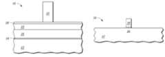
- FIG. 1Shown in FIG. 1 is a semiconductor device 10 comprising a semiconductor substrate 12 , an insulating layer 14 over substrate 12 , a conductive material 16 over insulating layer 14 , an organic ARC layer 18 over the conductive material 16 , a TEOS layer 20 over organic ARC layer 18 , and a patterned photoresist layer 22 .
- patterned photoresist layer 22is patterned for locating a gate of a MOS transistor.
- TEOS layer 20is an oxide layer made using TEOS preferably at a temperature of 300 degrees Celsius.
- An effective TEOS layerhas been deposited using an Applied Materials Centura 5200 DxZ deposition tool using TEOS, oxygen, and helium at 5.5 Torr.
- the flow ratesare 840 milligrams per minute (mgm) for TEOS, 840 sccm for the oxygen, and 560 sccm for the helium.
- the poweris set at 510 watts for the high frequency and 110 watts for the low frequency.
- This equipment and these settingsare exemplary and could be different.
- the temperatureis intentionally less than the typical deposition temperature of 400 degrees Celsius for TEOS.
- the temperatureis preferably lower than about 350 degrees Celsius.
- the temperatureshould also be greater than about 250 degrees Celsius. Other equipment would almost certainly run at somewhat different conditions and such settings would be determined by experimentation.
- substrate 12is silicon
- insulating layer 14is silicon oxide of about 15 Angstroms
- conductive material 16is polysilicon of about 1000 Angstroms
- organic ARC 18is an hydrogenated amorphous carbon film deposited by plasma enhanced chemical vapor deposition (PECVD) as is known to one of ordinary skill in the art and is 500 Angstroms thick
- patterned photoresist 22is 2500 Angstroms thick.
- a thinner photoresist at 1500 Angstromsmay be preferable.
- a polysilicon thickness of 1500 Angstromsmay be preferable.
- metalis used instead polysilicon, the thickness is preferably less than 1000 Angstroms.
- FIG. 2Shown in FIG. 2 is semiconductor device 10 after lateral thinning of patterned photoresist 22 to form thinned photoresist 24 .
- This lateral thinningis to reduce the width of the pattern. This is a technique for obtaining smaller geometries than can be exposed by the lithography equipment that is available.
- patterned photoresist 22is achieved by an exposure of 0.1 microns (100 nanometers).
- thinned photoresistis about 50 nanometers in width and reduced in thickness to about 1500 Angstroms.
- TEOS layer 20is minimally effected by this thinning process.
- FIG. 3Shown in FIG. 3 is semiconductor device 10 after TEOS layer 20 has been etched using thinned photoresist 24 as a mask to form a TEOS portion 26 under thinned photoresist 28 .
- FIG. 4Shown in FIG. 4 is semiconductor device 10 after organic ARC layer 18 has been etched using thinned photoresist 28 and TEOS portion 26 to form an ARC portion 30 .
- ARC portion 30is etched using a reactive ion etch. This etch is an anisotropic etch that becomes isotropic after the exposed portion of ARC 18 is removed. The isotropic effect results in undercutting ARC 18 under TEOS portion 26 to leave ARC portion 30 under TEOS portion 26 .
- Thisis a technique to further reduce the width of the ultimate layer that is to be formed from conductive layer 16 . This technique is known to one of ordinary skill in the art.
- FIG. 5Shown in FIG. 5 is a semiconductor device 10 after conductive material 16 is etched using ARC portion 30 as a mask to leave a gate conductor 34 of polysilicon and a ARC portion 36 , which is smaller than ARC portion 30 due to the exposure to etchants used to etch conductive layer 16 .
- This gate conductor 34could be a different material than polysilicon, such as metal.
- Metals that are being consideredinclude, but are not limited to, tantalum silicon nitride, titanium nitride, and tungsten. Further, metal gates may be combinations of layers and one of those layers may even include polysilicon in addition to one or more metal layers.
- FIG. 6Shown in FIG. 6 is a semiconductor device 10 after removal of ARC portion 36 and the portion of insulating layer 14 that is exposed in FIG. 5 to leave a gate dielectric 38 under gate conductor 34 .
- This removal of ARC portion 36is achieved using conventional processes for removing photoresist. Although there is no photoresist shown in FIG. 5 , there may be some remnant of photoresist and etch reactants left that are removed typically by ashing. This ashing is also effective in reacting away the material that is used for organic ARC 18 . A combination of wet cleans, such as a piranha and SCI, is also conventional which in combination with the ashing is certain to remove all of the ARC 18 material. Thus, there is no additional removal step required for removing ARC portion 36 .
- FIG. 7Shown in FIG. 7 is a semiconductor device 10 as a completed transistor after sidewall 40 formation and source 42 and drain 44 implants, which is formed in conventional manner after a gate conductor has been formed over a gate dielectric.
- this use of low temperature TEOSdoes not cause any unusual or extra steps in the transistor formation after gate formation.
- this low temperature TEOSis beneficial because it essentially eliminates photoresist poisoning that causes photoresist to not develop in areas where it is intended to be removed.
- the poisoninggenerally comes from nitrogen in the photoresist that neutralizes the acid in the photoresist. Because the TEOS has no nitrogen, there is no nitrogen to poison the photoresist.
- Another benefit of low temperature TEOSis that the photoresist adheres well to it. This is contrasted with conventional 400 degree TEOS from which the photoresist does tend to delaminate, especially for photoresists that are designed for 193 nanometer lithography. Also it retains good adherence to the underlying organic ARC layer.
- TEOSoptical properties
- n and k at 193 nanometersprovide, in combination with the organic ARC, effective anti-reflection properties.
- Another benefitis the ease of photolithography rework in the event of improper photoresist patterning in which case the photoresist needs to be removed and re-applied. In such event the TEOS does not need to be removed. Films directly under the photoresist that are etched when photoresist is removed would also have to be removed and re-applied. The TEOS layer does not have to be removed and re-applied in that situation. Further, it protects the organic ARC during the rework process.
- TEOSTEOS
- the organosilane and oxidizershould be nitrogen-free.
- TEOSis preferable at least because the chemicals for it are less expensive and tool availability is better.
- TEOSis also a very stable film. This stability may be difficult to match.
- a typical organosilane for this purposeis trimethylsilane.
- a typical oxidizerwould be either pure oxygen or carbon dioxide.
- TEOS solutionAnother alternative to the TEOS solution is to use silicon nitride in combination with one of silicon-rich oxynitride (SRON) and silicon-rich oxide (SRO).
- SRONsilicon-rich oxynitride
- SROsilicon-rich oxide
- the combinationwould be a composite layer that would replace TEOS layer 20 .
- the silicon nitride layerwould be on the organic ARC 16 and the SRON or SRO layer would be between the photoresist and the silicon nitride layer. This is effective in providing both the necessary adhesion and the low defectivity.
- the combinationwould be separated by the organic ARC.
- the silicon nitride layerwould be between the conductive layer 16 and the ARC layer 18 .
- the SRON or SRO layerwould be between the ARC layer 18 and the photoresist. This is also effective in providing adequate adhesion and defectivity.
Landscapes
- Engineering & Computer Science (AREA)
- Physics & Mathematics (AREA)
- Power Engineering (AREA)
- Condensed Matter Physics & Semiconductors (AREA)
- General Physics & Mathematics (AREA)
- Manufacturing & Machinery (AREA)
- Computer Hardware Design (AREA)
- Microelectronics & Electronic Packaging (AREA)
- Chemical & Material Sciences (AREA)
- Inorganic Chemistry (AREA)
- Chemical Kinetics & Catalysis (AREA)
- Plasma & Fusion (AREA)
- Internal Circuitry In Semiconductor Integrated Circuit Devices (AREA)
- Drying Of Semiconductors (AREA)
- Exposure Of Semiconductors, Excluding Electron Or Ion Beam Exposure (AREA)
- Electrodes Of Semiconductors (AREA)
- Insulated Gate Type Field-Effect Transistor (AREA)
Abstract
Description
Claims (2)
Priority Applications (1)
| Application Number | Priority Date | Filing Date | Title |
|---|---|---|---|
| US11/676,100US8039389B2 (en) | 2003-07-28 | 2007-02-16 | Semiconductor device having an organic anti-reflective coating (ARC) and method therefor |
Applications Claiming Priority (3)
| Application Number | Priority Date | Filing Date | Title |
|---|---|---|---|
| US10/628,668US6972255B2 (en) | 2003-07-28 | 2003-07-28 | Semiconductor device having an organic anti-reflective coating (ARC) and method therefor |
| US11/100,163US7199429B2 (en) | 2003-07-28 | 2005-04-06 | Semiconductor device having an organic anti-reflective coating (ARC) and method therefor |
| US11/676,100US8039389B2 (en) | 2003-07-28 | 2007-02-16 | Semiconductor device having an organic anti-reflective coating (ARC) and method therefor |
Related Parent Applications (1)
| Application Number | Title | Priority Date | Filing Date |
|---|---|---|---|
| US11/100,163DivisionUS7199429B2 (en) | 2003-07-28 | 2005-04-06 | Semiconductor device having an organic anti-reflective coating (ARC) and method therefor |
Publications (2)
| Publication Number | Publication Date |
|---|---|
| US20070141770A1 US20070141770A1 (en) | 2007-06-21 |
| US8039389B2true US8039389B2 (en) | 2011-10-18 |
Family
ID=34103421
Family Applications (3)
| Application Number | Title | Priority Date | Filing Date |
|---|---|---|---|
| US10/628,668Expired - LifetimeUS6972255B2 (en) | 2003-07-28 | 2003-07-28 | Semiconductor device having an organic anti-reflective coating (ARC) and method therefor |
| US11/100,163Expired - LifetimeUS7199429B2 (en) | 2003-07-28 | 2005-04-06 | Semiconductor device having an organic anti-reflective coating (ARC) and method therefor |
| US11/676,100Expired - LifetimeUS8039389B2 (en) | 2003-07-28 | 2007-02-16 | Semiconductor device having an organic anti-reflective coating (ARC) and method therefor |
Family Applications Before (2)
| Application Number | Title | Priority Date | Filing Date |
|---|---|---|---|
| US10/628,668Expired - LifetimeUS6972255B2 (en) | 2003-07-28 | 2003-07-28 | Semiconductor device having an organic anti-reflective coating (ARC) and method therefor |
| US11/100,163Expired - LifetimeUS7199429B2 (en) | 2003-07-28 | 2005-04-06 | Semiconductor device having an organic anti-reflective coating (ARC) and method therefor |
Country Status (7)
| Country | Link |
|---|---|
| US (3) | US6972255B2 (en) |
| EP (1) | EP1652225A4 (en) |
| JP (1) | JP4677407B2 (en) |
| KR (1) | KR101164690B1 (en) |
| CN (1) | CN100461350C (en) |
| TW (1) | TWI348777B (en) |
| WO (1) | WO2005013320A2 (en) |
Families Citing this family (22)
| Publication number | Priority date | Publication date | Assignee | Title |
|---|---|---|---|---|
| US6573030B1 (en)* | 2000-02-17 | 2003-06-03 | Applied Materials, Inc. | Method for depositing an amorphous carbon layer |
| US6972255B2 (en)* | 2003-07-28 | 2005-12-06 | Freescale Semiconductor, Inc. | Semiconductor device having an organic anti-reflective coating (ARC) and method therefor |
| DE10339988B4 (en)* | 2003-08-29 | 2008-06-12 | Advanced Micro Devices, Inc., Sunnyvale | Method for producing an antireflecting layer |
| US20060105567A1 (en)* | 2004-11-12 | 2006-05-18 | Intel Corporation | Method for forming a dual-damascene structure |
| US7176130B2 (en)* | 2004-11-12 | 2007-02-13 | Freescale Semiconductor, Inc. | Plasma treatment for surface of semiconductor device |
| US20070000360A1 (en)* | 2005-07-01 | 2007-01-04 | Colarelli Nicholas J Iii | Tool for an automobile brake lathe |
| US7829159B2 (en)* | 2005-12-16 | 2010-11-09 | Asm Japan K.K. | Method of forming organosilicon oxide film and multilayer resist structure |
| US7371695B2 (en)* | 2006-01-04 | 2008-05-13 | Promos Technologies Pte. Ltd. | Use of TEOS oxides in integrated circuit fabrication processes |
| JP2007311508A (en)* | 2006-05-17 | 2007-11-29 | Nikon Corp | Fine pattern forming method and device manufacturing method |
| JP2008091825A (en)* | 2006-10-05 | 2008-04-17 | Nec Electronics Corp | Manufacturing method of semiconductor device |
| US7727829B2 (en)* | 2007-02-06 | 2010-06-01 | Freescale Semiconductor, Inc. | Method of forming a semiconductor device having a removable sidewall spacer |
| US7737018B2 (en)* | 2007-02-06 | 2010-06-15 | Freescale Semiconductor, Inc. | Process of forming an electronic device including forming a gate electrode layer and forming a patterned masking layer |
| US20090104541A1 (en)* | 2007-10-23 | 2009-04-23 | Eui Kyoon Kim | Plasma surface treatment to prevent pattern collapse in immersion lithography |
| KR100983724B1 (en) | 2007-12-20 | 2010-09-24 | 주식회사 하이닉스반도체 | Method for manufacturing semiconductor device |
| US20090197086A1 (en)* | 2008-02-04 | 2009-08-06 | Sudha Rathi | Elimination of photoresist material collapse and poisoning in 45-nm feature size using dry or immersion lithography |
| CN102087993B (en)* | 2009-12-04 | 2013-01-23 | 中芯国际集成电路制造(上海)有限公司 | Groove forming method |
| CN102867742B (en)* | 2012-09-17 | 2015-06-24 | 上海华力微电子有限公司 | Plasma etching method for eliminating morphologic deformation |
| US9640430B2 (en) | 2015-09-17 | 2017-05-02 | Nxp Usa, Inc. | Semiconductor device with graphene encapsulated metal and method therefor |
| CN114256068B (en)* | 2016-06-14 | 2025-08-01 | 克罗米斯有限公司 | Engineered substrate structures for power applications and radio frequency applications |
| US10510582B2 (en)* | 2016-06-14 | 2019-12-17 | QROMIS, Inc. | Engineered substrate structure |
| US10297445B2 (en) | 2016-06-14 | 2019-05-21 | QROMIS, Inc. | Engineered substrate structure for power and RF applications |
| CN110660839B (en)* | 2019-11-13 | 2022-04-29 | 京东方科技集团股份有限公司 | Display panel and preparation method thereof |
Citations (40)
| Publication number | Priority date | Publication date | Assignee | Title |
|---|---|---|---|---|
| US5324676A (en)* | 1989-06-21 | 1994-06-28 | Xicor, Inc. | Method for forming a dual thickness dielectric floating gate memory cell |
| US5536681A (en) | 1995-06-23 | 1996-07-16 | Taiwan Semiconductor Manufacturing Company | PE-OX/ozone-TEOS gap filling capability by selective N2 treatment on PE-OX |
| US5635425A (en) | 1995-05-25 | 1997-06-03 | Industrial Technology Research Institute | In-situ N2 plasma treatment for PE TEOS oxide deposition |
| US5807660A (en) | 1997-02-03 | 1998-09-15 | Taiwan Semiconductor Manufacturing Company Ltd. | Avoid photoresist lifting by post-oxide-dep plasma treatment |
| US5880018A (en) | 1996-10-07 | 1999-03-09 | Motorola Inc. | Method for manufacturing a low dielectric constant inter-level integrated circuit structure |
| US5976992A (en) | 1993-09-27 | 1999-11-02 | Kabushiki Kaisha Toshiba | Method of supplying excited oxygen |
| US5998100A (en) | 1996-05-24 | 1999-12-07 | Kabushiki Kaisha Toshiba | Fabrication process using a multi-layer antireflective layer |
| WO2000031782A1 (en) | 1998-11-25 | 2000-06-02 | Advanced Micro Devices, Inc. | Silane-based oxide anti-reflective coating for patterning of metal features in semiconductor manufacturing |
| US6093973A (en) | 1998-09-30 | 2000-07-25 | Advanced Micro Devices, Inc. | Hard mask for metal patterning |
| US6143666A (en) | 1998-03-30 | 2000-11-07 | Vanguard International Seminconductor Company | Plasma surface treatment method for forming patterned TEOS based silicon oxide layer with reliable via and interconnection formed therethrough |
| US6159863A (en) | 1999-01-22 | 2000-12-12 | Advanced Micro Devices, Inc. | Insitu hardmask and metal etch in a single etcher |
| US6187687B1 (en) | 1998-11-05 | 2001-02-13 | Advanced Micro Devices, Inc. | Minimization of line width variation in photolithography |
| US6187688B1 (en) | 1997-01-21 | 2001-02-13 | Matsushita Electric Industrial Co., Ltd. | Pattern formation method |
| US6197687B1 (en)* | 1999-09-13 | 2001-03-06 | Advanced Micro Devices, Inc. | Method of patterning field dielectric regions in a semiconductor device |
| JP2001085407A (en) | 1999-09-13 | 2001-03-30 | Hitachi Ltd | Method and apparatus for manufacturing semiconductor integrated circuit device |
| US6211078B1 (en) | 1997-08-18 | 2001-04-03 | Micron Technology, Inc. | Method of improving resist adhesion for use in patterning conductive layers |
| US6214637B1 (en) | 1999-04-30 | 2001-04-10 | Samsung Electronics Co., Ltd. | Method of forming a photoresist pattern on a semiconductor substrate using an anti-reflective coating deposited using only a hydrocarbon based gas |
| US6306771B1 (en) | 1999-08-27 | 2001-10-23 | Integrated Device Technology, Inc. | Process for preventing the formation of ring defects |
| US20010036732A1 (en) | 2000-04-27 | 2001-11-01 | Nec Corporation | Method of manufacturing semiconductor device having minute gate electrodes |
| US6316167B1 (en) | 2000-01-10 | 2001-11-13 | International Business Machines Corporation | Tunabale vapor deposited materials as antireflective coatings, hardmasks and as combined antireflective coating/hardmasks and methods of fabrication thereof and application thereof |
| EP1154468A2 (en) | 2000-02-17 | 2001-11-14 | Applied Materials, Inc. | Method of depositing an amorphous carbon layer |
| JP2002012972A (en) | 2000-02-17 | 2002-01-15 | Applied Materials Inc | Method for depositing amorphous carbon layer |
| KR20020009109A (en) | 2000-07-24 | 2002-02-01 | 박종섭 | method for manufacturing of semiconductor device |
| US6417167B1 (en) | 1997-02-05 | 2002-07-09 | Kirin Beer Kabushiki Kaisha | Lyophilized compositions containing shingoglycolipid and process for preparing them |
| US6417084B1 (en) | 2000-07-20 | 2002-07-09 | Advanced Micro Devices, Inc. | T-gate formation using a modified conventional poly process |
| US6420097B1 (en)* | 2000-05-02 | 2002-07-16 | Advanced Micro Devices, Inc. | Hardmask trim process |
| US6423385B1 (en) | 1999-02-25 | 2002-07-23 | Hitachi, Ltd. | Liquid crystal display devices |
| US6423384B1 (en) | 1999-06-25 | 2002-07-23 | Applied Materials, Inc. | HDP-CVD deposition of low dielectric constant amorphous carbon film |
| US6428894B1 (en) | 1997-06-04 | 2002-08-06 | International Business Machines Corporation | Tunable and removable plasma deposited antireflective coatings |
| US6479315B1 (en) | 2000-11-27 | 2002-11-12 | Microscan Systems, Inc. | Process for manufacturing micromechanical and microoptomechanical structures with single crystal silicon exposure step |
| US6503818B1 (en) | 1999-04-02 | 2003-01-07 | Taiwan Semiconductor Manufacturing Company | Delamination resistant multi-layer composite dielectric layer employing low dielectric constant dielectric material |
| US6541397B1 (en) | 2002-03-29 | 2003-04-01 | Applied Materials, Inc. | Removable amorphous carbon CMP stop |
| US6548423B1 (en) | 2002-01-16 | 2003-04-15 | Advanced Micro Devices, Inc. | Multilayer anti-reflective coating process for integrated circuit fabrication |
| US6656830B1 (en) | 2001-02-07 | 2003-12-02 | Advanced Micro Devices, Inc. | Dual damascene with silicon carbide middle etch stop layer/ARC |
| US6716571B2 (en) | 2001-03-28 | 2004-04-06 | Advanced Micro Devices, Inc. | Selective photoresist hardening to facilitate lateral trimming |
| US6764949B2 (en) | 2002-07-31 | 2004-07-20 | Advanced Micro Devices, Inc. | Method for reducing pattern deformation and photoresist poisoning in semiconductor device fabrication |
| US6894342B1 (en) | 2003-06-12 | 2005-05-17 | Spansion Llc | Structure and method for preventing UV radiation damage in a memory cell and improving contact CD control |
| US6900002B1 (en) | 2002-11-19 | 2005-05-31 | Advanced Micro Devices, Inc. | Antireflective bi-layer hardmask including a densified amorphous carbon layer |
| US6972255B2 (en) | 2003-07-28 | 2005-12-06 | Freescale Semiconductor, Inc. | Semiconductor device having an organic anti-reflective coating (ARC) and method therefor |
| US7208423B2 (en) | 2001-03-29 | 2007-04-24 | Kabushiki Kaisha Toshiba | Semiconductor device fabrication method and semiconductor device |
Family Cites Families (8)
| Publication number | Priority date | Publication date | Assignee | Title |
|---|---|---|---|---|
| US5545588A (en)* | 1995-05-05 | 1996-08-13 | Taiwan Semiconductor Manufacturing Company | Method of using disposable hard mask for gate critical dimension control |
| US6133613A (en)* | 1998-02-03 | 2000-10-17 | Vanguard International Semiconductor Corporation | Anti-reflection oxynitride film for tungsten-silicide substrates |
| WO1999050894A1 (en)* | 1998-03-27 | 1999-10-07 | Advanced Micro Devices, Inc. | Thin oxide film for augmenting anti-reflectivity and eliminating resist footing |
| JP2002194547A (en)* | 2000-06-08 | 2002-07-10 | Applied Materials Inc | Method for depositing amorphous carbon layer |
| US6423364B1 (en)* | 2001-02-28 | 2002-07-23 | Protein Technologies International, Inc. | Functional food ingredient |
| JP4014891B2 (en)* | 2001-03-29 | 2007-11-28 | 株式会社東芝 | Manufacturing method of semiconductor device |
| JP2003077900A (en)* | 2001-09-06 | 2003-03-14 | Hitachi Ltd | Method for manufacturing semiconductor device |
| JP3877997B2 (en)* | 2001-11-05 | 2007-02-07 | プロモス テクノロジーズ インコーポレイテッド | Method for forming a dynamic random access memory cell |
- 2003
- 2003-07-28USUS10/628,668patent/US6972255B2/ennot_activeExpired - Lifetime
- 2004
- 2004-07-13CNCNB2004800173895Apatent/CN100461350C/ennot_activeExpired - Lifetime
- 2004-07-13JPJP2006521869Apatent/JP4677407B2/ennot_activeExpired - Lifetime
- 2004-07-13KRKR1020067001728Apatent/KR101164690B1/ennot_activeExpired - Lifetime
- 2004-07-13EPEP04778107Apatent/EP1652225A4/ennot_activeWithdrawn
- 2004-07-13WOPCT/US2004/022434patent/WO2005013320A2/enactiveApplication Filing
- 2004-07-19TWTW093121522Apatent/TWI348777B/ennot_activeIP Right Cessation
- 2005
- 2005-04-06USUS11/100,163patent/US7199429B2/ennot_activeExpired - Lifetime
- 2007
- 2007-02-16USUS11/676,100patent/US8039389B2/ennot_activeExpired - Lifetime
Patent Citations (42)
| Publication number | Priority date | Publication date | Assignee | Title |
|---|---|---|---|---|
| US5324676A (en)* | 1989-06-21 | 1994-06-28 | Xicor, Inc. | Method for forming a dual thickness dielectric floating gate memory cell |
| US5976992A (en) | 1993-09-27 | 1999-11-02 | Kabushiki Kaisha Toshiba | Method of supplying excited oxygen |
| US5635425A (en) | 1995-05-25 | 1997-06-03 | Industrial Technology Research Institute | In-situ N2 plasma treatment for PE TEOS oxide deposition |
| US5536681A (en) | 1995-06-23 | 1996-07-16 | Taiwan Semiconductor Manufacturing Company | PE-OX/ozone-TEOS gap filling capability by selective N2 treatment on PE-OX |
| US5998100A (en) | 1996-05-24 | 1999-12-07 | Kabushiki Kaisha Toshiba | Fabrication process using a multi-layer antireflective layer |
| US5880018A (en) | 1996-10-07 | 1999-03-09 | Motorola Inc. | Method for manufacturing a low dielectric constant inter-level integrated circuit structure |
| US6187688B1 (en) | 1997-01-21 | 2001-02-13 | Matsushita Electric Industrial Co., Ltd. | Pattern formation method |
| US5807660A (en) | 1997-02-03 | 1998-09-15 | Taiwan Semiconductor Manufacturing Company Ltd. | Avoid photoresist lifting by post-oxide-dep plasma treatment |
| US6417167B1 (en) | 1997-02-05 | 2002-07-09 | Kirin Beer Kabushiki Kaisha | Lyophilized compositions containing shingoglycolipid and process for preparing them |
| US6428894B1 (en) | 1997-06-04 | 2002-08-06 | International Business Machines Corporation | Tunable and removable plasma deposited antireflective coatings |
| US6211078B1 (en) | 1997-08-18 | 2001-04-03 | Micron Technology, Inc. | Method of improving resist adhesion for use in patterning conductive layers |
| US6143666A (en) | 1998-03-30 | 2000-11-07 | Vanguard International Seminconductor Company | Plasma surface treatment method for forming patterned TEOS based silicon oxide layer with reliable via and interconnection formed therethrough |
| US6093973A (en) | 1998-09-30 | 2000-07-25 | Advanced Micro Devices, Inc. | Hard mask for metal patterning |
| US6187687B1 (en) | 1998-11-05 | 2001-02-13 | Advanced Micro Devices, Inc. | Minimization of line width variation in photolithography |
| WO2000031782A1 (en) | 1998-11-25 | 2000-06-02 | Advanced Micro Devices, Inc. | Silane-based oxide anti-reflective coating for patterning of metal features in semiconductor manufacturing |
| JP2002530885A (en) | 1998-11-25 | 2002-09-17 | アドバンスト・マイクロ・ディバイシズ・インコーポレイテッド | Silane-based oxide anti-reflective coating for patterning metal features in semiconductor manufacturing |
| JP2002535847A (en) | 1999-01-22 | 2002-10-22 | アドバンスト・マイクロ・ディバイシズ・インコーポレイテッド | Method for in-situ etching of hard mask and metal layer in a single etcher |
| US6159863A (en) | 1999-01-22 | 2000-12-12 | Advanced Micro Devices, Inc. | Insitu hardmask and metal etch in a single etcher |
| US6423385B1 (en) | 1999-02-25 | 2002-07-23 | Hitachi, Ltd. | Liquid crystal display devices |
| US6503818B1 (en) | 1999-04-02 | 2003-01-07 | Taiwan Semiconductor Manufacturing Company | Delamination resistant multi-layer composite dielectric layer employing low dielectric constant dielectric material |
| US6214637B1 (en) | 1999-04-30 | 2001-04-10 | Samsung Electronics Co., Ltd. | Method of forming a photoresist pattern on a semiconductor substrate using an anti-reflective coating deposited using only a hydrocarbon based gas |
| US6423384B1 (en) | 1999-06-25 | 2002-07-23 | Applied Materials, Inc. | HDP-CVD deposition of low dielectric constant amorphous carbon film |
| US6306771B1 (en) | 1999-08-27 | 2001-10-23 | Integrated Device Technology, Inc. | Process for preventing the formation of ring defects |
| US6197687B1 (en)* | 1999-09-13 | 2001-03-06 | Advanced Micro Devices, Inc. | Method of patterning field dielectric regions in a semiconductor device |
| JP2001085407A (en) | 1999-09-13 | 2001-03-30 | Hitachi Ltd | Method and apparatus for manufacturing semiconductor integrated circuit device |
| US6316167B1 (en) | 2000-01-10 | 2001-11-13 | International Business Machines Corporation | Tunabale vapor deposited materials as antireflective coatings, hardmasks and as combined antireflective coating/hardmasks and methods of fabrication thereof and application thereof |
| EP1154468A2 (en) | 2000-02-17 | 2001-11-14 | Applied Materials, Inc. | Method of depositing an amorphous carbon layer |
| JP2002012972A (en) | 2000-02-17 | 2002-01-15 | Applied Materials Inc | Method for depositing amorphous carbon layer |
| US20010036732A1 (en) | 2000-04-27 | 2001-11-01 | Nec Corporation | Method of manufacturing semiconductor device having minute gate electrodes |
| US6420097B1 (en)* | 2000-05-02 | 2002-07-16 | Advanced Micro Devices, Inc. | Hardmask trim process |
| US6417084B1 (en) | 2000-07-20 | 2002-07-09 | Advanced Micro Devices, Inc. | T-gate formation using a modified conventional poly process |
| KR20020009109A (en) | 2000-07-24 | 2002-02-01 | 박종섭 | method for manufacturing of semiconductor device |
| US6479315B1 (en) | 2000-11-27 | 2002-11-12 | Microscan Systems, Inc. | Process for manufacturing micromechanical and microoptomechanical structures with single crystal silicon exposure step |
| US6656830B1 (en) | 2001-02-07 | 2003-12-02 | Advanced Micro Devices, Inc. | Dual damascene with silicon carbide middle etch stop layer/ARC |
| US6716571B2 (en) | 2001-03-28 | 2004-04-06 | Advanced Micro Devices, Inc. | Selective photoresist hardening to facilitate lateral trimming |
| US7208423B2 (en) | 2001-03-29 | 2007-04-24 | Kabushiki Kaisha Toshiba | Semiconductor device fabrication method and semiconductor device |
| US6548423B1 (en) | 2002-01-16 | 2003-04-15 | Advanced Micro Devices, Inc. | Multilayer anti-reflective coating process for integrated circuit fabrication |
| US6541397B1 (en) | 2002-03-29 | 2003-04-01 | Applied Materials, Inc. | Removable amorphous carbon CMP stop |
| US6764949B2 (en) | 2002-07-31 | 2004-07-20 | Advanced Micro Devices, Inc. | Method for reducing pattern deformation and photoresist poisoning in semiconductor device fabrication |
| US6900002B1 (en) | 2002-11-19 | 2005-05-31 | Advanced Micro Devices, Inc. | Antireflective bi-layer hardmask including a densified amorphous carbon layer |
| US6894342B1 (en) | 2003-06-12 | 2005-05-17 | Spansion Llc | Structure and method for preventing UV radiation damage in a memory cell and improving contact CD control |
| US6972255B2 (en) | 2003-07-28 | 2005-12-06 | Freescale Semiconductor, Inc. | Semiconductor device having an organic anti-reflective coating (ARC) and method therefor |
Non-Patent Citations (6)
| Title |
|---|
| Notice of Allowance mailed Sep. 21, 2006 in U.S. Appl. No. 10/987,790. |
| Office Action mailed Feb. 6, 2006 in U.S. Appl. No. 10/987,790. |
| PCT Application PCT/US2004/022434, Search Report and Written Opinion, mailed Jan. 28, 2005. |
| Search report for corresponding EPC Application No. 04778107.5-1235. |
| U.S. Appl. No. 60/183,507, filed Feb. 17, 2000. |
| Widmann et al; "Technologie hochintegrierter Schaltungen"; 1996 Springer Verlag, pp. 63-64. |
Also Published As
| Publication number | Publication date |
|---|---|
| CN1809916A (en) | 2006-07-26 |
| TWI348777B (en) | 2011-09-11 |
| WO2005013320A3 (en) | 2005-04-07 |
| TW200520274A (en) | 2005-06-16 |
| KR20060056346A (en) | 2006-05-24 |
| US20050181596A1 (en) | 2005-08-18 |
| JP4677407B2 (en) | 2011-04-27 |
| US20050026338A1 (en) | 2005-02-03 |
| WO2005013320A2 (en) | 2005-02-10 |
| US20070141770A1 (en) | 2007-06-21 |
| US7199429B2 (en) | 2007-04-03 |
| CN100461350C (en) | 2009-02-11 |
| KR101164690B1 (en) | 2012-07-11 |
| JP2007500443A (en) | 2007-01-11 |
| EP1652225A4 (en) | 2009-05-13 |
| US6972255B2 (en) | 2005-12-06 |
| EP1652225A2 (en) | 2006-05-03 |
Similar Documents
| Publication | Publication Date | Title |
|---|---|---|
| US8039389B2 (en) | Semiconductor device having an organic anti-reflective coating (ARC) and method therefor | |
| TWI821329B (en) | Patterning scheme to improve euv resist and hard mask selectivity | |
| US6030541A (en) | Process for defining a pattern using an anti-reflective coating and structure therefor | |
| US7811924B2 (en) | Air gap formation and integration using a patterning cap | |
| KR101476435B1 (en) | Multi-layer resist plasma etch method | |
| US5750441A (en) | Mask having a tapered profile used during the formation of a semiconductor device | |
| US7390750B1 (en) | Method of patterning elements within a semiconductor topography | |
| US20080197109A1 (en) | Etch pattern definition using a CVD organic layer as an anti-reflection coating and hardmask | |
| US8293460B2 (en) | Double exposure patterning with carbonaceous hardmask | |
| US20080293248A1 (en) | Method of forming amorphous carbon film and method of manufacturing semiconductor device using the same | |
| US20090163030A1 (en) | Semiconductor device manufacturing method | |
| US7901869B2 (en) | Double patterning with a double layer cap on carbonaceous hardmask | |
| KR20070107017A (en) | Line edge roughness reduction method compatible with trimming | |
| JP2007110112A (en) | Carbon-containing film etching method and semiconductor device manufacturing method using the same | |
| US6607986B2 (en) | Dry etching method and semiconductor device manufacturing method | |
| US7189643B2 (en) | Semiconductor device and method of fabricating the same | |
| US20010030169A1 (en) | Method of etching organic film and method of producing element | |
| US20080194107A1 (en) | Method of manufacturing semiconductor device | |
| US7067429B2 (en) | Processing method of forming MRAM circuitry | |
| US7176130B2 (en) | Plasma treatment for surface of semiconductor device | |
| JP3725811B2 (en) | Manufacturing method of semiconductor device | |
| JP3877461B2 (en) | Manufacturing method of semiconductor device | |
| JP2873759B2 (en) | Pretreatment method for wet etching of semiconductor device | |
| KR19980060902A (en) | METHOD FOR FORMING METAL WIRING OF SEMICONDUCTOR | |
| EP1320877A2 (en) | Silicon oxide patterning using cvd photoresist |
Legal Events
| Date | Code | Title | Description |
|---|---|---|---|
| AS | Assignment | Owner name:CITIBANK, N.A., NEW YORK Free format text:SECURITY AGREEMENT;ASSIGNOR:FREESCALE SEMICONDUCTOR, INC.;REEL/FRAME:019847/0804 Effective date:20070620 Owner name:CITIBANK, N.A.,NEW YORK Free format text:SECURITY AGREEMENT;ASSIGNOR:FREESCALE SEMICONDUCTOR, INC.;REEL/FRAME:019847/0804 Effective date:20070620 | |
| AS | Assignment | Owner name:CITIBANK, N.A.,NEW YORK Free format text:SECURITY AGREEMENT;ASSIGNOR:FREESCALE SEMICONDUCTOR, INC.;REEL/FRAME:024085/0001 Effective date:20100219 Owner name:CITIBANK, N.A., NEW YORK Free format text:SECURITY AGREEMENT;ASSIGNOR:FREESCALE SEMICONDUCTOR, INC.;REEL/FRAME:024085/0001 Effective date:20100219 | |
| AS | Assignment | Owner name:CITIBANK, N.A., AS COLLATERAL AGENT,NEW YORK Free format text:SECURITY AGREEMENT;ASSIGNOR:FREESCALE SEMICONDUCTOR, INC.;REEL/FRAME:024397/0001 Effective date:20100413 Owner name:CITIBANK, N.A., AS COLLATERAL AGENT, NEW YORK Free format text:SECURITY AGREEMENT;ASSIGNOR:FREESCALE SEMICONDUCTOR, INC.;REEL/FRAME:024397/0001 Effective date:20100413 | |
| STCF | Information on status: patent grant | Free format text:PATENTED CASE | |
| AS | Assignment | Owner name:CITIBANK, N.A., AS NOTES COLLATERAL AGENT, NEW YORK Free format text:SECURITY AGREEMENT;ASSIGNOR:FREESCALE SEMICONDUCTOR, INC.;REEL/FRAME:030633/0424 Effective date:20130521 Owner name:CITIBANK, N.A., AS NOTES COLLATERAL AGENT, NEW YOR Free format text:SECURITY AGREEMENT;ASSIGNOR:FREESCALE SEMICONDUCTOR, INC.;REEL/FRAME:030633/0424 Effective date:20130521 | |
| AS | Assignment | Owner name:CITIBANK, N.A., AS NOTES COLLATERAL AGENT, NEW YORK Free format text:SECURITY AGREEMENT;ASSIGNOR:FREESCALE SEMICONDUCTOR, INC.;REEL/FRAME:031591/0266 Effective date:20131101 Owner name:CITIBANK, N.A., AS NOTES COLLATERAL AGENT, NEW YOR Free format text:SECURITY AGREEMENT;ASSIGNOR:FREESCALE SEMICONDUCTOR, INC.;REEL/FRAME:031591/0266 Effective date:20131101 | |
| FPAY | Fee payment | Year of fee payment:4 | |
| AS | Assignment | Owner name:FREESCALE SEMICONDUCTOR, INC., TEXAS Free format text:PATENT RELEASE;ASSIGNOR:CITIBANK, N.A., AS COLLATERAL AGENT;REEL/FRAME:037354/0640 Effective date:20151207 Owner name:FREESCALE SEMICONDUCTOR, INC., TEXAS Free format text:PATENT RELEASE;ASSIGNOR:CITIBANK, N.A., AS COLLATERAL AGENT;REEL/FRAME:037356/0553 Effective date:20151207 Owner name:FREESCALE SEMICONDUCTOR, INC., TEXAS Free format text:PATENT RELEASE;ASSIGNOR:CITIBANK, N.A., AS COLLATERAL AGENT;REEL/FRAME:037356/0143 Effective date:20151207 | |
| AS | Assignment | Owner name:MORGAN STANLEY SENIOR FUNDING, INC., MARYLAND Free format text:ASSIGNMENT AND ASSUMPTION OF SECURITY INTEREST IN PATENTS;ASSIGNOR:CITIBANK, N.A.;REEL/FRAME:037486/0517 Effective date:20151207 | |
| AS | Assignment | Owner name:MORGAN STANLEY SENIOR FUNDING, INC., MARYLAND Free format text:ASSIGNMENT AND ASSUMPTION OF SECURITY INTEREST IN PATENTS;ASSIGNOR:CITIBANK, N.A.;REEL/FRAME:037518/0292 Effective date:20151207 | |
| AS | Assignment | Owner name:ADVANCED MICRO DEVICES, INC., CALIFORNIA Free format text:ASSIGNMENT OF ASSIGNORS INTEREST;ASSIGNOR:FREESCALE SEMICONDUCTOR, INC.;REEL/FRAME:037599/0364 Effective date:20151201 | |
| AS | Assignment | Owner name:MORGAN STANLEY SENIOR FUNDING, INC., MARYLAND Free format text:SECURITY AGREEMENT SUPPLEMENT;ASSIGNOR:NXP B.V.;REEL/FRAME:038017/0058 Effective date:20160218 | |
| AS | Assignment | Owner name:MORGAN STANLEY SENIOR FUNDING, INC., MARYLAND Free format text:CORRECTIVE ASSIGNMENT TO CORRECT THE REMOVE APPLICATION 12092129 PREVIOUSLY RECORDED ON REEL 038017 FRAME 0058. ASSIGNOR(S) HEREBY CONFIRMS THE SECURITY AGREEMENT SUPPLEMENT;ASSIGNOR:NXP B.V.;REEL/FRAME:039361/0212 Effective date:20160218 | |
| AS | Assignment | Owner name:NXP B.V., NETHERLANDS Free format text:PATENT RELEASE;ASSIGNOR:MORGAN STANLEY SENIOR FUNDING, INC.;REEL/FRAME:039707/0471 Effective date:20160805 | |
| AS | Assignment | Owner name:NXP, B.V., F/K/A FREESCALE SEMICONDUCTOR, INC., NETHERLANDS Free format text:RELEASE BY SECURED PARTY;ASSIGNOR:MORGAN STANLEY SENIOR FUNDING, INC.;REEL/FRAME:040925/0001 Effective date:20160912 Owner name:NXP, B.V., F/K/A FREESCALE SEMICONDUCTOR, INC., NE Free format text:RELEASE BY SECURED PARTY;ASSIGNOR:MORGAN STANLEY SENIOR FUNDING, INC.;REEL/FRAME:040925/0001 Effective date:20160912 | |
| AS | Assignment | Owner name:NXP B.V., NETHERLANDS Free format text:RELEASE BY SECURED PARTY;ASSIGNOR:MORGAN STANLEY SENIOR FUNDING, INC.;REEL/FRAME:040928/0001 Effective date:20160622 | |
| AS | Assignment | Owner name:MORGAN STANLEY SENIOR FUNDING, INC., MARYLAND Free format text:CORRECTIVE ASSIGNMENT TO CORRECT THE REMOVE PATENTS 8108266 AND 8062324 AND REPLACE THEM WITH 6108266 AND 8060324 PREVIOUSLY RECORDED ON REEL 037518 FRAME 0292. ASSIGNOR(S) HEREBY CONFIRMS THE ASSIGNMENT AND ASSUMPTION OF SECURITY INTEREST IN PATENTS;ASSIGNOR:CITIBANK, N.A.;REEL/FRAME:041703/0536 Effective date:20151207 | |
| AS | Assignment | Owner name:MORGAN STANLEY SENIOR FUNDING, INC., MARYLAND Free format text:CORRECTIVE ASSIGNMENT TO CORRECT THE REMOVE APPLICATION 12681366 PREVIOUSLY RECORDED ON REEL 039361 FRAME 0212. ASSIGNOR(S) HEREBY CONFIRMS THE SECURITY AGREEMENT SUPPLEMENT;ASSIGNOR:NXP B.V.;REEL/FRAME:042762/0145 Effective date:20160218 Owner name:MORGAN STANLEY SENIOR FUNDING, INC., MARYLAND Free format text:CORRECTIVE ASSIGNMENT TO CORRECT THE REMOVE APPLICATION 12681366 PREVIOUSLY RECORDED ON REEL 038017 FRAME 0058. ASSIGNOR(S) HEREBY CONFIRMS THE SECURITY AGREEMENT SUPPLEMENT;ASSIGNOR:NXP B.V.;REEL/FRAME:042985/0001 Effective date:20160218 | |
| AS | Assignment | Owner name:SHENZHEN XINGUODU TECHNOLOGY CO., LTD., CHINA Free format text:CORRECTIVE ASSIGNMENT TO CORRECT THE TO CORRECT THE APPLICATION NO. FROM 13,883,290 TO 13,833,290 PREVIOUSLY RECORDED ON REEL 041703 FRAME 0536. ASSIGNOR(S) HEREBY CONFIRMS THE THE ASSIGNMENT AND ASSUMPTION OF SECURITYINTEREST IN PATENTS.;ASSIGNOR:MORGAN STANLEY SENIOR FUNDING, INC.;REEL/FRAME:048734/0001 Effective date:20190217 | |
| MAFP | Maintenance fee payment | Free format text:PAYMENT OF MAINTENANCE FEE, 8TH YEAR, LARGE ENTITY (ORIGINAL EVENT CODE: M1552); ENTITY STATUS OF PATENT OWNER: LARGE ENTITY Year of fee payment:8 | |
| AS | Assignment | Owner name:NXP B.V., NETHERLANDS Free format text:RELEASE BY SECURED PARTY;ASSIGNOR:MORGAN STANLEY SENIOR FUNDING, INC.;REEL/FRAME:050745/0001 Effective date:20190903 | |
| AS | Assignment | Owner name:MORGAN STANLEY SENIOR FUNDING, INC., MARYLAND Free format text:CORRECTIVE ASSIGNMENT TO CORRECT THE REMOVE APPLICATION 12298143 PREVIOUSLY RECORDED ON REEL 042985 FRAME 0001. ASSIGNOR(S) HEREBY CONFIRMS THE SECURITY AGREEMENT SUPPLEMENT;ASSIGNOR:NXP B.V.;REEL/FRAME:051029/0001 Effective date:20160218 Owner name:MORGAN STANLEY SENIOR FUNDING, INC., MARYLAND Free format text:CORRECTIVE ASSIGNMENT TO CORRECT THE REMOVE APPLICATION 12298143 PREVIOUSLY RECORDED ON REEL 042762 FRAME 0145. ASSIGNOR(S) HEREBY CONFIRMS THE SECURITY AGREEMENT SUPPLEMENT;ASSIGNOR:NXP B.V.;REEL/FRAME:051145/0184 Effective date:20160218 Owner name:MORGAN STANLEY SENIOR FUNDING, INC., MARYLAND Free format text:CORRECTIVE ASSIGNMENT TO CORRECT THE REMOVE APPLICATION 12298143 PREVIOUSLY RECORDED ON REEL 039361 FRAME 0212. ASSIGNOR(S) HEREBY CONFIRMS THE SECURITY AGREEMENT SUPPLEMENT;ASSIGNOR:NXP B.V.;REEL/FRAME:051029/0387 Effective date:20160218 Owner name:MORGAN STANLEY SENIOR FUNDING, INC., MARYLAND Free format text:CORRECTIVE ASSIGNMENT TO CORRECT THE REMOVE APPLICATION 12298143 PREVIOUSLY RECORDED ON REEL 038017 FRAME 0058. ASSIGNOR(S) HEREBY CONFIRMS THE SECURITY AGREEMENT SUPPLEMENT;ASSIGNOR:NXP B.V.;REEL/FRAME:051030/0001 Effective date:20160218 Owner name:MORGAN STANLEY SENIOR FUNDING, INC., MARYLAND Free format text:CORRECTIVE ASSIGNMENT TO CORRECT THE REMOVE APPLICATION12298143 PREVIOUSLY RECORDED ON REEL 042985 FRAME 0001. ASSIGNOR(S) HEREBY CONFIRMS THE SECURITY AGREEMENT SUPPLEMENT;ASSIGNOR:NXP B.V.;REEL/FRAME:051029/0001 Effective date:20160218 Owner name:MORGAN STANLEY SENIOR FUNDING, INC., MARYLAND Free format text:CORRECTIVE ASSIGNMENT TO CORRECT THE REMOVE APPLICATION12298143 PREVIOUSLY RECORDED ON REEL 039361 FRAME 0212. ASSIGNOR(S) HEREBY CONFIRMS THE SECURITY AGREEMENT SUPPLEMENT;ASSIGNOR:NXP B.V.;REEL/FRAME:051029/0387 Effective date:20160218 Owner name:MORGAN STANLEY SENIOR FUNDING, INC., MARYLAND Free format text:CORRECTIVE ASSIGNMENT TO CORRECT THE REMOVE APPLICATION12298143 PREVIOUSLY RECORDED ON REEL 042762 FRAME 0145. ASSIGNOR(S) HEREBY CONFIRMS THE SECURITY AGREEMENT SUPPLEMENT;ASSIGNOR:NXP B.V.;REEL/FRAME:051145/0184 Effective date:20160218 | |
| AS | Assignment | Owner name:MORGAN STANLEY SENIOR FUNDING, INC., MARYLAND Free format text:CORRECTIVE ASSIGNMENT TO CORRECT THE REMOVE APPLICATION11759915 AND REPLACE IT WITH APPLICATION 11759935 PREVIOUSLY RECORDED ON REEL 037486 FRAME 0517. ASSIGNOR(S) HEREBY CONFIRMS THE ASSIGNMENT AND ASSUMPTION OF SECURITYINTEREST IN PATENTS;ASSIGNOR:CITIBANK, N.A.;REEL/FRAME:053547/0421 Effective date:20151207 | |
| AS | Assignment | Owner name:NXP B.V., NETHERLANDS Free format text:CORRECTIVE ASSIGNMENT TO CORRECT THE REMOVEAPPLICATION 11759915 AND REPLACE IT WITH APPLICATION11759935 PREVIOUSLY RECORDED ON REEL 040928 FRAME 0001. ASSIGNOR(S) HEREBY CONFIRMS THE RELEASE OF SECURITYINTEREST;ASSIGNOR:MORGAN STANLEY SENIOR FUNDING, INC.;REEL/FRAME:052915/0001 Effective date:20160622 | |
| AS | Assignment | Owner name:NXP, B.V. F/K/A FREESCALE SEMICONDUCTOR, INC., NETHERLANDS Free format text:CORRECTIVE ASSIGNMENT TO CORRECT THE REMOVEAPPLICATION 11759915 AND REPLACE IT WITH APPLICATION11759935 PREVIOUSLY RECORDED ON REEL 040925 FRAME 0001. ASSIGNOR(S) HEREBY CONFIRMS THE RELEASE OF SECURITYINTEREST;ASSIGNOR:MORGAN STANLEY SENIOR FUNDING, INC.;REEL/FRAME:052917/0001 Effective date:20160912 | |
| MAFP | Maintenance fee payment | Free format text:PAYMENT OF MAINTENANCE FEE, 12TH YEAR, LARGE ENTITY (ORIGINAL EVENT CODE: M1553); ENTITY STATUS OF PATENT OWNER: LARGE ENTITY Year of fee payment:12 |