US8039348B2 - Vertical gated access transistor - Google Patents
Vertical gated access transistorDownload PDFInfo
- Publication number
- US8039348B2 US8039348B2US12/785,712US78571210AUS8039348B2US 8039348 B2US8039348 B2US 8039348B2US 78571210 AUS78571210 AUS 78571210AUS 8039348 B2US8039348 B2US 8039348B2
- Authority
- US
- United States
- Prior art keywords
- region
- trenches
- substrate
- layer
- etching
- Prior art date
- Legal status (The legal status is an assumption and is not a legal conclusion. Google has not performed a legal analysis and makes no representation as to the accuracy of the status listed.)
- Active
Links
- 238000000034methodMethods0.000claimsabstractdescription96
- 239000000758substrateSubstances0.000claimsabstractdescription83
- 238000005530etchingMethods0.000claimsabstractdescription31
- 238000000151depositionMethods0.000claimsabstractdescription18
- 230000000873masking effectEffects0.000claimsabstractdescription17
- 239000004020conductorSubstances0.000claimsabstractdescription16
- 239000000463materialSubstances0.000claimsdescription63
- 239000004065semiconductorSubstances0.000claimsdescription63
- 125000006850spacer groupChemical group0.000claimsdescription52
- 229910021420polycrystalline siliconInorganic materials0.000claimsdescription16
- 229910052751metalInorganic materials0.000claimsdescription9
- 239000002184metalSubstances0.000claimsdescription9
- 229910021332silicideInorganic materials0.000claimsdescription7
- FVBUAEGBCNSCDD-UHFFFAOYSA-Nsilicide(4-)Chemical group[Si-4]FVBUAEGBCNSCDD-UHFFFAOYSA-N0.000claimsdescription7
- 239000007769metal materialSubstances0.000claimsdescription3
- 239000011810insulating materialSubstances0.000claims2
- 239000007772electrode materialSubstances0.000claims1
- 150000004767nitridesChemical class0.000description23
- 229910052581Si3N4Inorganic materials0.000description15
- XUIMIQQOPSSXEZ-UHFFFAOYSA-NSiliconChemical compound[Si]XUIMIQQOPSSXEZ-UHFFFAOYSA-N0.000description15
- 229910052710siliconInorganic materials0.000description15
- 239000010703siliconSubstances0.000description15
- 238000000059patterningMethods0.000description14
- 238000000206photolithographyMethods0.000description14
- 238000004519manufacturing processMethods0.000description12
- WQJQOUPTWCFRMM-UHFFFAOYSA-Ntungsten disilicideChemical compound[Si]#[W]#[Si]WQJQOUPTWCFRMM-UHFFFAOYSA-N0.000description10
- 229910021342tungsten silicideInorganic materials0.000description10
- 239000003990capacitorSubstances0.000description8
- 238000010276constructionMethods0.000description8
- HQVNEWCFYHHQES-UHFFFAOYSA-Nsilicon nitrideChemical compoundN12[Si]34N5[Si]62N3[Si]51N64HQVNEWCFYHHQES-UHFFFAOYSA-N0.000description7
- VYPSYNLAJGMNEJ-UHFFFAOYSA-NSilicium dioxideChemical compoundO=[Si]=OVYPSYNLAJGMNEJ-UHFFFAOYSA-N0.000description6
- 230000008021depositionEffects0.000description6
- 230000001965increasing effectEffects0.000description6
- 238000005240physical vapour depositionMethods0.000description6
- 238000005137deposition processMethods0.000description5
- 230000002829reductive effectEffects0.000description5
- 230000010354integrationEffects0.000description4
- 238000001020plasma etchingMethods0.000description4
- 229910052814silicon oxideInorganic materials0.000description4
- 238000003860storageMethods0.000description4
- WGTYBPLFGIVFAS-UHFFFAOYSA-Mtetramethylammonium hydroxideChemical compound[OH-].C[N+](C)(C)CWGTYBPLFGIVFAS-UHFFFAOYSA-M0.000description4
- 238000011109contaminationMethods0.000description3
- 239000003989dielectric materialSubstances0.000description3
- 230000002093peripheral effectEffects0.000description3
- 239000000126substanceSubstances0.000description3
- BOTDANWDWHJENH-UHFFFAOYSA-NTetraethyl orthosilicateChemical compoundCCO[Si](OCC)(OCC)OCCBOTDANWDWHJENH-UHFFFAOYSA-N0.000description2
- 230000000694effectsEffects0.000description2
- 239000000945fillerSubstances0.000description2
- 229920002120photoresistant polymerPolymers0.000description2
- 238000000926separation methodMethods0.000description2
- 230000003068static effectEffects0.000description2
- 230000001360synchronised effectEffects0.000description2
- 229910052715tantalumInorganic materials0.000description2
- GUVRBAGPIYLISA-UHFFFAOYSA-Ntantalum atomChemical compound[Ta]GUVRBAGPIYLISA-UHFFFAOYSA-N0.000description2
- OKTJSMMVPCPJKN-UHFFFAOYSA-NCarbonChemical compound[C]OKTJSMMVPCPJKN-UHFFFAOYSA-N0.000description1
- KJTLSVCANCCWHF-UHFFFAOYSA-NRutheniumChemical compound[Ru]KJTLSVCANCCWHF-UHFFFAOYSA-N0.000description1
- 229910020286SiOxNyInorganic materials0.000description1
- RTAQQCXQSZGOHL-UHFFFAOYSA-NTitaniumChemical compound[Ti]RTAQQCXQSZGOHL-UHFFFAOYSA-N0.000description1
- NRTOMJZYCJJWKI-UHFFFAOYSA-NTitanium nitrideChemical compound[Ti]#NNRTOMJZYCJJWKI-UHFFFAOYSA-N0.000description1
- 229910003481amorphous carbonInorganic materials0.000description1
- 238000003491arrayMethods0.000description1
- QVGXLLKOCUKJST-UHFFFAOYSA-Natomic oxygenChemical compound[O]QVGXLLKOCUKJST-UHFFFAOYSA-N0.000description1
- 230000015572biosynthetic processEffects0.000description1
- 229910052799carbonInorganic materials0.000description1
- 239000005387chalcogenide glassSubstances0.000description1
- 238000003486chemical etchingMethods0.000description1
- 238000005229chemical vapour depositionMethods0.000description1
- 229910017052cobaltInorganic materials0.000description1
- 239000010941cobaltSubstances0.000description1
- GUTLYIVDDKVIGB-UHFFFAOYSA-Ncobalt atomChemical compound[Co]GUTLYIVDDKVIGB-UHFFFAOYSA-N0.000description1
- 239000013078crystalSubstances0.000description1
- 239000002019doping agentSubstances0.000description1
- 230000002708enhancing effectEffects0.000description1
- 230000006870functionEffects0.000description1
- 239000007943implantSubstances0.000description1
- 238000002955isolationMethods0.000description1
- 230000000670limiting effectEffects0.000description1
- 238000001465metallisationMethods0.000description1
- 150000002739metalsChemical class0.000description1
- 239000000203mixtureSubstances0.000description1
- 229910003465moissaniteInorganic materials0.000description1
- 229910021421monocrystalline siliconInorganic materials0.000description1
- 229910021334nickel silicideInorganic materials0.000description1
- RUFLMLWJRZAWLJ-UHFFFAOYSA-Nnickel silicideChemical compound[Ni]=[Si]=[Ni]RUFLMLWJRZAWLJ-UHFFFAOYSA-N0.000description1
- 230000003287optical effectEffects0.000description1
- 230000003647oxidationEffects0.000description1
- 238000007254oxidation reactionMethods0.000description1
- 229910052760oxygenInorganic materials0.000description1
- 239000001301oxygenSubstances0.000description1
- 230000036961partial effectEffects0.000description1
- 230000005855radiationEffects0.000description1
- 229910052707rutheniumInorganic materials0.000description1
- 229910010271silicon carbideInorganic materials0.000description1
- 235000012239silicon dioxideNutrition0.000description1
- 239000000377silicon dioxideSubstances0.000description1
- WNUPENMBHHEARK-UHFFFAOYSA-Nsilicon tungstenChemical compound[Si].[W]WNUPENMBHHEARK-UHFFFAOYSA-N0.000description1
- 238000000992sputter etchingMethods0.000description1
- MZLGASXMSKOWSE-UHFFFAOYSA-Ntantalum nitrideChemical compound[Ta]#NMZLGASXMSKOWSE-UHFFFAOYSA-N0.000description1
- 229910052719titaniumInorganic materials0.000description1
- 239000010936titaniumSubstances0.000description1
- 229910021341titanium silicideInorganic materials0.000description1
- WFKWXMTUELFFGS-UHFFFAOYSA-NtungstenChemical compound[W]WFKWXMTUELFFGS-UHFFFAOYSA-N0.000description1
- 229910052721tungstenInorganic materials0.000description1
- 239000010937tungstenSubstances0.000description1
Images


Classifications
- H—ELECTRICITY
- H10—SEMICONDUCTOR DEVICES; ELECTRIC SOLID-STATE DEVICES NOT OTHERWISE PROVIDED FOR
- H10D—INORGANIC ELECTRIC SEMICONDUCTOR DEVICES
- H10D84/00—Integrated devices formed in or on semiconductor substrates that comprise only semiconducting layers, e.g. on Si wafers or on GaAs-on-Si wafers
- H10D84/01—Manufacture or treatment
- H10D84/0123—Integrating together multiple components covered by H10D12/00 or H10D30/00, e.g. integrating multiple IGBTs
- H10D84/0126—Integrating together multiple components covered by H10D12/00 or H10D30/00, e.g. integrating multiple IGBTs the components including insulated gates, e.g. IGFETs
- H10D84/0158—Integrating together multiple components covered by H10D12/00 or H10D30/00, e.g. integrating multiple IGBTs the components including insulated gates, e.g. IGFETs the components including FinFETs
- H—ELECTRICITY
- H01—ELECTRIC ELEMENTS
- H01L—SEMICONDUCTOR DEVICES NOT COVERED BY CLASS H10
- H01L21/00—Processes or apparatus adapted for the manufacture or treatment of semiconductor or solid state devices or of parts thereof
- H01L21/70—Manufacture or treatment of devices consisting of a plurality of solid state components formed in or on a common substrate or of parts thereof; Manufacture of integrated circuit devices or of parts thereof
- H01L21/71—Manufacture of specific parts of devices defined in group H01L21/70
- H01L21/76—Making of isolation regions between components
- H01L21/762—Dielectric regions, e.g. EPIC dielectric isolation, LOCOS; Trench refilling techniques, SOI technology, use of channel stoppers
- H01L21/76224—Dielectric regions, e.g. EPIC dielectric isolation, LOCOS; Trench refilling techniques, SOI technology, use of channel stoppers using trench refilling with dielectric materials
- H01L21/76229—Concurrent filling of a plurality of trenches having a different trench shape or dimension, e.g. rectangular and V-shaped trenches, wide and narrow trenches, shallow and deep trenches
- H—ELECTRICITY
- H01—ELECTRIC ELEMENTS
- H01L—SEMICONDUCTOR DEVICES NOT COVERED BY CLASS H10
- H01L21/00—Processes or apparatus adapted for the manufacture or treatment of semiconductor or solid state devices or of parts thereof
- H01L21/70—Manufacture or treatment of devices consisting of a plurality of solid state components formed in or on a common substrate or of parts thereof; Manufacture of integrated circuit devices or of parts thereof
- H01L21/71—Manufacture of specific parts of devices defined in group H01L21/70
- H01L21/76—Making of isolation regions between components
- H01L21/762—Dielectric regions, e.g. EPIC dielectric isolation, LOCOS; Trench refilling techniques, SOI technology, use of channel stoppers
- H01L21/76224—Dielectric regions, e.g. EPIC dielectric isolation, LOCOS; Trench refilling techniques, SOI technology, use of channel stoppers using trench refilling with dielectric materials
- H01L21/76232—Dielectric regions, e.g. EPIC dielectric isolation, LOCOS; Trench refilling techniques, SOI technology, use of channel stoppers using trench refilling with dielectric materials of trenches having a shape other than rectangular or V-shape, e.g. rounded corners, oblique or rounded trench walls
- H—ELECTRICITY
- H10—SEMICONDUCTOR DEVICES; ELECTRIC SOLID-STATE DEVICES NOT OTHERWISE PROVIDED FOR
- H10B—ELECTRONIC MEMORY DEVICES
- H10B12/00—Dynamic random access memory [DRAM] devices
- H10B12/01—Manufacture or treatment
- H10B12/02—Manufacture or treatment for one transistor one-capacitor [1T-1C] memory cells
- H10B12/05—Making the transistor
- H10B12/053—Making the transistor the transistor being at least partially in a trench in the substrate
- H—ELECTRICITY
- H10—SEMICONDUCTOR DEVICES; ELECTRIC SOLID-STATE DEVICES NOT OTHERWISE PROVIDED FOR
- H10B—ELECTRONIC MEMORY DEVICES
- H10B12/00—Dynamic random access memory [DRAM] devices
- H10B12/01—Manufacture or treatment
- H10B12/02—Manufacture or treatment for one transistor one-capacitor [1T-1C] memory cells
- H10B12/05—Making the transistor
- H10B12/056—Making the transistor the transistor being a FinFET
- H—ELECTRICITY
- H10—SEMICONDUCTOR DEVICES; ELECTRIC SOLID-STATE DEVICES NOT OTHERWISE PROVIDED FOR
- H10B—ELECTRONIC MEMORY DEVICES
- H10B12/00—Dynamic random access memory [DRAM] devices
- H10B12/01—Manufacture or treatment
- H10B12/09—Manufacture or treatment with simultaneous manufacture of the peripheral circuit region and memory cells
- H—ELECTRICITY
- H10—SEMICONDUCTOR DEVICES; ELECTRIC SOLID-STATE DEVICES NOT OTHERWISE PROVIDED FOR
- H10B—ELECTRONIC MEMORY DEVICES
- H10B12/00—Dynamic random access memory [DRAM] devices
- H10B12/30—DRAM devices comprising one-transistor - one-capacitor [1T-1C] memory cells
- H10B12/34—DRAM devices comprising one-transistor - one-capacitor [1T-1C] memory cells the transistor being at least partially in a trench in the substrate
- H—ELECTRICITY
- H10—SEMICONDUCTOR DEVICES; ELECTRIC SOLID-STATE DEVICES NOT OTHERWISE PROVIDED FOR
- H10B—ELECTRONIC MEMORY DEVICES
- H10B12/00—Dynamic random access memory [DRAM] devices
- H10B12/30—DRAM devices comprising one-transistor - one-capacitor [1T-1C] memory cells
- H10B12/36—DRAM devices comprising one-transistor - one-capacitor [1T-1C] memory cells the transistor being a FinFET
- H—ELECTRICITY
- H10—SEMICONDUCTOR DEVICES; ELECTRIC SOLID-STATE DEVICES NOT OTHERWISE PROVIDED FOR
- H10D—INORGANIC ELECTRIC SEMICONDUCTOR DEVICES
- H10D30/00—Field-effect transistors [FET]
- H10D30/01—Manufacture or treatment
- H10D30/021—Manufacture or treatment of FETs having insulated gates [IGFET]
- H10D30/024—Manufacture or treatment of FETs having insulated gates [IGFET] of fin field-effect transistors [FinFET]
- H—ELECTRICITY
- H10—SEMICONDUCTOR DEVICES; ELECTRIC SOLID-STATE DEVICES NOT OTHERWISE PROVIDED FOR
- H10D—INORGANIC ELECTRIC SEMICONDUCTOR DEVICES
- H10D30/00—Field-effect transistors [FET]
- H10D30/60—Insulated-gate field-effect transistors [IGFET]
- H10D30/62—Fin field-effect transistors [FinFET]
- H10D30/6211—Fin field-effect transistors [FinFET] having fin-shaped semiconductor bodies integral with the bulk semiconductor substrates
- H—ELECTRICITY
- H10—SEMICONDUCTOR DEVICES; ELECTRIC SOLID-STATE DEVICES NOT OTHERWISE PROVIDED FOR
- H10D—INORGANIC ELECTRIC SEMICONDUCTOR DEVICES
- H10D30/00—Field-effect transistors [FET]
- H10D30/60—Insulated-gate field-effect transistors [IGFET]
- H10D30/63—Vertical IGFETs
- H—ELECTRICITY
- H10—SEMICONDUCTOR DEVICES; ELECTRIC SOLID-STATE DEVICES NOT OTHERWISE PROVIDED FOR
- H10D—INORGANIC ELECTRIC SEMICONDUCTOR DEVICES
- H10D64/00—Electrodes of devices having potential barriers
- H10D64/01—Manufacture or treatment
- H10D64/017—Manufacture or treatment using dummy gates in processes wherein at least parts of the final gates are self-aligned to the dummy gates, i.e. replacement gate processes
- H—ELECTRICITY
- H10—SEMICONDUCTOR DEVICES; ELECTRIC SOLID-STATE DEVICES NOT OTHERWISE PROVIDED FOR
- H10D—INORGANIC ELECTRIC SEMICONDUCTOR DEVICES
- H10D84/00—Integrated devices formed in or on semiconductor substrates that comprise only semiconducting layers, e.g. on Si wafers or on GaAs-on-Si wafers
- H10D84/01—Manufacture or treatment
- H10D84/0123—Integrating together multiple components covered by H10D12/00 or H10D30/00, e.g. integrating multiple IGBTs
- H10D84/0126—Integrating together multiple components covered by H10D12/00 or H10D30/00, e.g. integrating multiple IGBTs the components including insulated gates, e.g. IGFETs
- H10D84/0135—Manufacturing their gate conductors
- H—ELECTRICITY
- H10—SEMICONDUCTOR DEVICES; ELECTRIC SOLID-STATE DEVICES NOT OTHERWISE PROVIDED FOR
- H10D—INORGANIC ELECTRIC SEMICONDUCTOR DEVICES
- H10D84/00—Integrated devices formed in or on semiconductor substrates that comprise only semiconducting layers, e.g. on Si wafers or on GaAs-on-Si wafers
- H10D84/01—Manufacture or treatment
- H10D84/0123—Integrating together multiple components covered by H10D12/00 or H10D30/00, e.g. integrating multiple IGBTs
- H10D84/0126—Integrating together multiple components covered by H10D12/00 or H10D30/00, e.g. integrating multiple IGBTs the components including insulated gates, e.g. IGFETs
- H10D84/0151—Manufacturing their isolation regions
- H—ELECTRICITY
- H10—SEMICONDUCTOR DEVICES; ELECTRIC SOLID-STATE DEVICES NOT OTHERWISE PROVIDED FOR
- H10D—INORGANIC ELECTRIC SEMICONDUCTOR DEVICES
- H10D84/00—Integrated devices formed in or on semiconductor substrates that comprise only semiconducting layers, e.g. on Si wafers or on GaAs-on-Si wafers
- H10D84/01—Manufacture or treatment
- H10D84/02—Manufacture or treatment characterised by using material-based technologies
- H10D84/03—Manufacture or treatment characterised by using material-based technologies using Group IV technology, e.g. silicon technology or silicon-carbide [SiC] technology
- H10D84/038—Manufacture or treatment characterised by using material-based technologies using Group IV technology, e.g. silicon technology or silicon-carbide [SiC] technology using silicon technology, e.g. SiGe
- H—ELECTRICITY
- H10—SEMICONDUCTOR DEVICES; ELECTRIC SOLID-STATE DEVICES NOT OTHERWISE PROVIDED FOR
- H10D—INORGANIC ELECTRIC SEMICONDUCTOR DEVICES
- H10D84/00—Integrated devices formed in or on semiconductor substrates that comprise only semiconducting layers, e.g. on Si wafers or on GaAs-on-Si wafers
- H10D84/80—Integrated devices formed in or on semiconductor substrates that comprise only semiconducting layers, e.g. on Si wafers or on GaAs-on-Si wafers characterised by the integration of at least one component covered by groups H10D12/00 or H10D30/00, e.g. integration of IGFETs
- H10D84/82—Integrated devices formed in or on semiconductor substrates that comprise only semiconducting layers, e.g. on Si wafers or on GaAs-on-Si wafers characterised by the integration of at least one component covered by groups H10D12/00 or H10D30/00, e.g. integration of IGFETs of only field-effect components
- H10D84/83—Integrated devices formed in or on semiconductor substrates that comprise only semiconducting layers, e.g. on Si wafers or on GaAs-on-Si wafers characterised by the integration of at least one component covered by groups H10D12/00 or H10D30/00, e.g. integration of IGFETs of only field-effect components of only insulated-gate FETs [IGFET]
- H—ELECTRICITY
- H10—SEMICONDUCTOR DEVICES; ELECTRIC SOLID-STATE DEVICES NOT OTHERWISE PROVIDED FOR
- H10D—INORGANIC ELECTRIC SEMICONDUCTOR DEVICES
- H10D30/00—Field-effect transistors [FET]
- H10D30/60—Insulated-gate field-effect transistors [IGFET]
- H10D30/62—Fin field-effect transistors [FinFET]
- H10D30/6212—Fin field-effect transistors [FinFET] having fin-shaped semiconductor bodies having non-rectangular cross-sections
Definitions
- the present inventionrelates generally to methods for forming semiconductor structures, and relates more specifically to improved methods for forming vertical transistor devices.
- Transistorsare used in many different types of integrated circuits, including memory devices and processors.
- a typical transistorcomprises a source, a drain, and a gate formed at the substrate surface.
- vertical transistor constructionsthat consume less substrate “real estate”, and thus that facilitate increasing the level of device integration, have been developed. Examples of vertical transistor constructions are disclosed in U.S. patent application Ser. No. 10/933,062, now U.S. Pat. No. 7,442,976, the entire disclosure of which is hereby incorporated by reference herein. While these improved transistor constructions are smaller and are packed more densely, they also often involve fabrication processes that are significantly more complex, therefore increasing fabrication time and expense.
- Fabrication complexityis increased even further when high density vertical transistors are formed in an array on the same substrate as logic circuitry that is positioned adjacent to the transistor array.
- conventional fabrication techniquesuse separate masks to independently define features in the device array region and in the device periphery region, since different process steps and materials are used to define the devices of these two regions.
- DRAMdynamic random access memory
- Conventional semiconductor-based electronic storage devicessuch as dynamic random access memory (“DRAM”) devices, include large numbers of transistor and capacitor elements that are grouped into memory cells.
- the memory cells that comprise a DRAM deviceare arranged into larger memory arrays that often comprise thousands, if not millions, of individual memory cells. Therefore, there is a continuing effort to reduce the complexity of the processes used to form densely-packed integrated circuit elements such as vertical transistor constructions.
- the methodfurther comprises removing the plurality of lines from the first region of the substrate, thereby creating a plurality of exposed areas from which the plurality of lines were removed.
- the methodfurther comprises etching a plurality of elongate trenches in the plurality of exposed areas while the second region of the substrate is masked.
- an apparatuscomprises a semiconductor substrate having an array portion and a logic portion.
- the apparatusfurther comprises at least one U-shaped semiconductor structure formed in the substrate array portion.
- the semiconductor structurecomprises a first source/drain region positioned atop a first pillar, a second source/drain region positioned atop a second pillar, and a U-shaped channel connecting the first and second source/drain regions.
- the U-shaped channelis contiguous with the semiconductor substrate.
- the methodfurther comprises at least one transistor device formed over the substrate logic portion, the transistor device including a gate dielectric layer and a gate material. The gate dielectric layer is elevated with respect to the first and second source/drain regions.
- a methodcomprises patterning a first plurality of semiconductor structures in an array portion of a semiconductor substrate using a first photolithographic mask.
- the methodfurther comprises patterning a second plurality of semiconductor structures over a logic portion of a semiconductor substrate using a second photolithographic mask.
- the methodfurther comprises patterning a sacrificial layer over the first plurality of semiconductor structures using the second photolithographic mask. The sacrificial layer is patterned simultaneously with the second plurality of semiconductor structures.
- a methodcomprises providing a semiconductor substrate having a first region and a second region. The method further comprises depositing a conductive layer over the substrate first and second regions. The method further comprises patterning the conductive layer deposited over the substrate first and second regions. The method further comprises using the patterned conductive layer to form a planar transistor structure over the substrate second region. The method further comprises using the patterned conductive layer in a masking process in the substrate first region.
- a partially-formed integrated circuitcomprises a first plurality of features comprising a first material and formed over a first portion of a substrate. The first plurality of features are separated from each other by a first spacing.
- the partially-formed integrated circuitfurther comprises a second plurality of features comprising a second material and formed over a second portion of the substrate. The first plurality of features and the second plurality of features are formed simultaneously. The first material is the same as the second material.
- the partially-formed integrated circuitfurther comprises a gap fill structure positioned between and contacting a selected two of the first plurality of features.
- the partially-formed integrated circuitfurther comprises a plurality of sidewall spacers positioned adjacent the second plurality of features. Adjacent sidewall spacers are separated from each other by a separation region. The plurality of sidewall spacers and the gap fill structure comprise the same material.
- a memory devicecomprises a substrate having an array portion and a logic portion.
- the memory devicefurther comprises a plurality of semiconductor structures that are recessed in the array portion of the substrate.
- the memory devicefurther comprises a plurality of transistor devices formed over the logic portion of the substrate.
- the transistor devicesinclude a gate oxide layer, an uncapped gate layer, and a sidewall spacer structure.
- the transistor devicesare formed in a layer that is below the plurality of semiconductor structures.
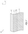
- FIG. 1illustrates a perspective view of a partially-formed semiconductor device usable to form an array of transistors.
- FIG. 2illustrates a cross-sectional view in the yz plane of the partially-formed semiconductor device of FIG. 1 , after the formation of additional semiconductor processing layers.
- FIG. 3illustrates a partial top plan view of an exemplary embodiment of a photo mask to be applied to the partially-formed semiconductor device of FIG. 1 .
- FIG. 4illustrates a cross-sectional view in the yz plane of the partially-formed semiconductor device of FIG. 2 after the photo mask of FIG. 3 has been applied and transferred to pattern the hard mask layer.
- FIG. 5illustrates a cross-sectional view in the yz plane of the partially-formed semiconductor device of FIG. 4 after blanket depositing a layer of spacer material thereover.
- FIG. 6illustrates a cross-sectional view in the yz plane of the partially-formed semiconductor device of FIG. 5 after performing a directional etch of the spacer material.
- FIG. 7illustrates a cross-sectional view in the yz plane of the partially-formed semiconductor device of FIG. 6 after etching a plurality of deep trenches into the substrate.
- FIG. 9illustrates a cross-sectional view in the yz plane of the partially-formed semiconductor device of FIG. 8 after patterning a hard mask layer thereover.
- FIG. 11illustrates a cross-sectional view in the yz plane of the partially-formed semiconductor device of FIG. 10 after etching a plurality of shallow trenches into the substrate.
- FIG. 12illustrates a cross-sectional view in the yz plane of the partially-formed semiconductor device of FIG. 11 after filling the shallow trenches with a dielectric material and providing the device with a substantially planar surface.
- FIG. 13illustrates a top-down view in the xy plane of the partially-formed semiconductor device of FIG. 12 .
- FIG. 15illustrates a cross-sectional view in the xz plane of the partially-formed semiconductor device of FIG. 14 , taken along line 15 - 15 , after depositing gate stack layers thereover.
- FIG. 16illustrates a cross-sectional view in the xz plane of the partially-formed semiconductor device of FIG. 15 after patterning active devices in the periphery region and lines in the array region.
- FIG. 18illustrates a cross-sectional view in the xz plane of the partially-formed semiconductor device of FIG. 17 after masking the device periphery region and etching gate stack layers from the unmasked array portions of the device.
- FIG. 19illustrates a cross-sectional view in the xz plane of the partially-formed semiconductor device of FIG. 18 after shrinking the remaining spacer material using a isotropic etch.
- FIG. 21illustrates a cross-sectional view in the xz plane of the partially-formed semiconductor device of FIG. 20 after removing remaining spacer material from the array region, lining the intermediate trenches with a dielectric, and forming sidewall spacers of gate material in the intermediate trenches.
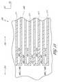
- FIG. 22illustrates a perspective view of a portion of the partially-formed semiconductor device of FIG. 21 .
- FIG. 25illustrates a cross-sectional view in the yz plane of the partially-formed semiconductor device of FIG. 8 after etching the nitride layer in the array region.
- FIG. 27is a schematic plan view of a memory device that illustrates the position of a memory cell with respect to an array of bit lines and word lines.
- vertical transistor constructionsadvantageously enable increased levels of device integration.
- the fabrication techniques disclosed hereinadvantageously use (a) fewer masking processes as compared to conventional fabrication techniques, and/or (b) masking processes that are easier to align.
- certain of the embodiments disclosed hereinadvantageously enable the forming of active devices in the periphery region and patterning features (for example, intermediate trenches separating rows of transistors) in the array region with a single mask.
- certain embodiments of the vertical transistors disclosed hereinhave a U-shaped configuration, wherein the channel connecting the source and drain regions is directly connected to the underlying substrate. This advantageously reduces or eliminates the floating body effect that is common in conventional vertical pillar transistors.
- the U-shaped vertical transistor configurations disclosed hereinprovide several advantages over conventional planar transistors. In addition to consuming less substrate “real estate”, certain of the U-shaped vertical transistor configurations disclosed herein form continuous rows and columns during fabrication, thereby enhancing the structural stability of the device. Certain embodiments of the fabrication techniques disclosed herein also advantageously allow use of a simplified reticle set to perform the masking processes employed to fabricate the memory array. Specifically, one embodiment of the reticle set used to fabricate such an array contains parallel lines and spaces, thereby facilitating printing and alignment of the masking processes.
- pitch doubling techniquesare used to form relatively smaller devices in an array region
- conventional photolithography techniquesare used to form relatively larger devices in a periphery region.
- structures having a feature size between 1 ⁇ 2F and 3 ⁇ 4Fare formed in the array region
- structures having a feature size of F or largerare formed in the periphery region, wherein F is the minimum resolvable feature size obtainable using a given photolithography technique.
- an epitaxial layer 104is grown on the substrate 110 .
- the epitaxial layer 104is a semiconductor layer (for example, comprising silicon) grown on the substrate 110 by an epitaxial growth process that extends the crystal structure of the substrate 110 .
- the epitaxial layer 104has a thickness that is preferably between about 2 ⁇ m and about 6 ⁇ m, and more preferably between about 3 ⁇ m and about 5 ⁇ m. In embodiments wherein the epitaxial layer 104 is grown on the substrate 110 before the subsequent etching steps described herein, the epitaxial layer 104 is considered part of the substrate 110 .
- the epitaxial layer 104is heavily doped with a conductivity type that is opposite that of the substrate 110 , thereby enabling the epitaxial layer 104 to serve as an active area for transistors formed thereover, as will be better understood from the final structures disclosed herein.
- the doped implant regionsinclude a lightly doped p ⁇ region that is positioned underneath a heavily doped p + region.
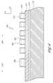
- FIG. 2illustrates a cross-section in the yz plane of the device of FIG. 1 after deposition of additional layers over the substrate 110 .
- the semiconductor device 100further comprises an oxide layer 210 formed over the substrate 110 and the optional epitaxial layer 104 .
- the oxide layer 210is selectively etchable with respect to the material comprising the substrate 110 and silicon nitride.
- the oxide layer 210comprises silicon dioxide and has a thickness that is preferably between about 100 ⁇ and 500 ⁇ , and more preferably between about 200 ⁇ and about 300 ⁇ .
- the oxide layer 210is a pad oxide layer having a thickness of approximately 200 ⁇ .
- the oxide layer 210is deposited using a suitable deposition process, such as chemical vapor deposition (“CVD”) or physical vapor deposition (“PVD”), or is grown by oxidation of the underlying substrate.
- CVDchemical vapor deposition
- PVDphysical vapor deposition
- the semiconductor device 100further comprises a layer, such as the illustrated nitride layer 211 , formed over the oxide layer 210 .
- the nitride layer 211comprises silicon nitride and has a thickness that is preferably between about 200 ⁇ and 2000 ⁇ , and more preferably between about 500 ⁇ and 1000 ⁇ .
- the nitride layer 211is deposited using a suitable deposition process, such as CVD or PVD.
- the semiconductor device 100further comprises a further hard mask layer 212 that is formed over the nitride layer 211 .
- the hard mask layer 212comprises amorphous carbon.
- the hard mask layer 212comprises transparent carbon, tetraethylorthosilicate (“TEOS”), polycrystalline silicon, Si 3 N 4 , SiO x N y , SiC, or another suitable hard mask material.
- TEOStetraethylorthosilicate
- the hard mask layer 212is deposited using a suitable deposition process, such as CVD or PVD.
- the optional epitaxial layer 104is omitted from subsequent illustrations.
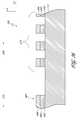
- FIG. 3illustrates a portion of a photo mask 300 to be applied to the device 100 to pattern the underlying hard mask layer 212 .
- the shaded portion of the photo mask 300represents the area in which the hard mask layer 212 will be removed after applying photolithography and etching techniques, and the unshaded portion represents the area in which the hard mask layer 212 will remain.
- the photo mask 300is a clear field mask that is configured to define a pattern of active area lines 304 separated from each other by gaps 302 in an array region 308 .
- the lines 304 and the gaps 302are approximately 1100 ⁇ to approximately 1300 ⁇ wide.
- the lines 304 and the gaps 302are approximately 1200 ⁇ wide.
- the photo mask 300optionally includes a wider line 306 that is provided for optical proximity correction.
- the gaps 302are used as a contact area for shallow trench isolation.
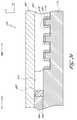
- FIG. 4illustrates a cross-section in the yz plane of the device of FIG. 2 after applying the photo mask 300 , illustrated in FIG. 3 , to pattern the hard mask layer 212 .
- the photo mask 300is applied and transferred to the hard mask layer 212 , such that the lines 304 and gaps 302 extend parallel to the x axis.
- the hard mask layer 212remains over areas of the substrate 110 where the photo mask 300 forms lines 304 , including the wider line 306 , and is removed form areas of the substrate 110 where the photo mask 300 forms gaps 302 .
- lines 304 and gaps 302are located in an array region 308 of the device, which is surrounded by a periphery region 310 of the device.
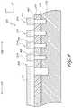
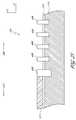
- FIG. 5illustrates a cross-section in the yz plane of the device of FIG. 4 after blanket depositing a layer of spacer material 214 thereover.
- the spacer material 214comprises an oxide material, such as silicon oxide having a thickness that is preferably between about 200 ⁇ and about 500 ⁇ , and more preferably between about 300 ⁇ and about 400 ⁇ .
- the spacer material 214fills approximately 1/20 to approximately 1 ⁇ 3 of the horizontal dimension of the gaps 302 .
- the spacer material 214is deposited using a suitable deposition process, such as CVD or PVD.
- FIG. 7illustrates a cross-section in the yz plane of the device of FIG. 6 after etching a plurality of deep trenches 400 through the nitride layer 211 and the oxide layer 210 , and into the substrate 110 .
- the pattern of deep trenches 400is defined according to the gaps 302 between the spacers in the device array region 308 .
- the deep trenches 400are etched using a process such as ion milling, reactive ion etching (“RIE”), or chemical etching.
- RIEis a directional anisotropic etch having both physical and chemical components.
- RIEreactive ion etching
- RIEis a directional anisotropic etch having both physical and chemical components.
- a chemical etchantsuch as RIE
- a variety of etchantsare usable, such as Cl 2 .
- the deep trenches 400are etched to a depth of between about 3000 ⁇ and about 5000 ⁇ based on gaps 302 , and are etched to a depth of between about 4000 ⁇ and about 5000 ⁇ adjacent to the wider line 306 .
- the etching technique used to define the deep trenchescauses the trench depth to be directly proportional to the trench width.
- FIG. 8illustrates a cross-section in the yz plane of the device of FIG. 7 after filling the deep trenches 400 with a spin on dielectric (“SOD”) material 408 .
- SODspin on dielectric
- An oxygen plasma techniqueis used to burn off the remaining hard mask layer 212
- CMPchemical mechanical polish
- the CMP techniquealso provides the device 100 with a substantially planar surface 402 in the xy plane. As illustrated, the substantially planar surface 402 extends across the device array region 308 and periphery region 310 .
- the deep trenches 400are separated by remaining portions of the nitride layer 211 ; in a preferred embodiment, the deep trenches are separated by between approximately 1600 ⁇ and approximately 2000 ⁇ of nitride material. In an exemplary embodiment, the deep trenches 400 are separated by approximately 1800 ⁇ of nitride material. In another exemplary embodiment, the deep trenches 400 are separated by 2.25 ⁇ F, wherein F is the minimum resolvable feature size obtainable using a given photolithography technique.
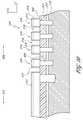
- FIG. 9illustrates a cross-section in the yz plane of the device of FIG. 8 after patterning another hard mask layer 312 over the deep trenches 400 .
- the hard mask layer 312is patterned based on a mask similar to that illustrated in FIG. 3 , and is patterned using photolithography and etching techniques.
- the patterned hard mask layer 312defines a plurality of lines 314 over the planar surface 402 , with the lines 314 effectively masking the deep trenches 400 .
- the lines 314are separated by a plurality of gaps 318 .
- the lines 314are between about 1100 ⁇ and about 1300 ⁇ wide, and in an exemplary embodiment, the lines are approximately 1200 ⁇ wide.
- the lines 314have substantially the same width as the lines 304 formed in the masking process illustrated in FIGS. 3 and 4 .
- the spacer loops 316which have a width approximately equal to the thickness of the original blanket spacer material deposition, effectively narrow the width of the gaps 318 .
- the gaps 318have a reduced width of between about 500 ⁇ and about 700 ⁇ after the spacer loops 316 are formed. In an exemplary embodiment, the gaps 318 have a reduced width of about 600 ⁇ after the spacer loops 316 are formed.
- FIG. 12illustrates a cross-section in the yz plane of the device of FIG. 11 after filling the shallow trenches 404 with a SOD material 410 .
- the shallow trenchesare optionally filled with the same SOD material 408 used to fill the deep trenches 400 .
- a CMP techniqueis used to remove the remaining hard mask layer 312 , spacer loops 316 , and excess SOD material.
- the CMP techniqueis used to reduce the thickness of the nitride layer 211 to between about 300 ⁇ and about 500 ⁇ .
- the CMP techniqueis used to reduce the thickness of the nitride layer 211 to about 400 ⁇ .
- the CMP techniquealso provides the device 100 with a substantially planar surface 406 in the xy plane. As illustrated, the substantially planar surface 406 extends across the device array region 308 and periphery region 310 .
- FIG. 13illustrates a top-down view in the xy plane of the device 100 of FIG. 12 .
- the device 100 illustrated in FIGS. 12 and 13comprises a plurality of elongate shallow trenches 404 that are separated from each other by elongate nitride spacers with looped ends, as defined by the remaining nitride layer 211 .
- the nitride spacersare separated from each other by the elongate deep trenches 400 .
- FIG. 14illustrates a cross-section in the yz plane of the device of FIGS. 12 and 13 after removal of the remaining nitride layer 211 and oxide layer 210 .
- the remaining portions of these layersare removed using an etching process, although other techniques are used in other embodiments.
- Subsequently performing a CMP techniqueresults in a substantially planar surface of alternating silicon regions and oxide regions.
- the silicon regionsdefine a plurality of elongate loops 112 that extend parallel to the x axis.
- the elongate loops 112surround shallow trenches 404 , and are separated from each other by the deep trenches 400 .
- the elongate loops 112are separated into individual transistor pillars by etching the loops perpendicular to their length, that is, parallel to the y axis.
- active devicesare formed in the device periphery region 310 using the same masking sequence that is used to etch the elongate loops 112 into individual transistor pillars.
- active device layersare blanket deposited over the device illustrated in FIG. 14 .
- FIG. 15illustrates a cross-section in the xz plane of the device of FIG. 14 after forming an oxide layer 450 , a polycrystalline silicon layer 452 , and a tungsten silicide layer 454 .
- the blanket oxide layer 450has a thickness between about 50 ⁇ and 80 ⁇ .
- other metallic materialsare used in place of tungsten silicide to strap peripheral gates and improve lateral signal speed.
- an optional blanket silicon nitride layer(not shown) is formed over the tungsten silicide layer 454 .
- the polycrystalline silicon layer 452comprises a conductive material, wherein the term “conductive material” includes silicon, even if undoped as deposited.
- FIG. 16illustrates a cross-section in the xz plane of the device of FIG. 15 after patterning the blanket-deposited layers.
- the layersare patterned using photolithography and masking techniques.
- one or more active devices 460are formed in the periphery region 310 .
- the active devicescomprise a stack including a gate oxide 462 , a polycrystalline silicon active area 464 , and a tungsten silicide strapping layer 466 .
- the strapping layer 466comprises other metallic materials, such as tungsten, titanium nitride, tantalum, and tantalum nitride. Mixtures of metals are also suitable for forming the strapping layer 466 .
- the same photolithography and masking technique that is used to form active devices 460 in the periphery regionis used to pattern a series of lines 470 in the array region 308 .
- the array lines 470comprise the same materials as the peripheral active devices 460 , although the array lines 470 are used as a sacrificial mask to pattern the underlying elongate loops 112 in subsequent processing steps. Additionally, the pattern of lines 470 in the array region 308 has a smaller pitch as compared to the pattern of active devices 460 in the periphery region 310 .
- the lines 470are spaced apart by a spacing F, wherein the active devices 460 are spaced apart by a spacing 2F, wherein F is the minimum resolvable feature size obtainable using a given photolithography technique.
- the active devices 460have a spacing that is between about two times and about four times larger than the spacing for lines 470 .
- the array lines 470which extend parallel to the y axis, are perpendicular to the elongate loops 112 , which extend parallel to the x axis.
- FIG. 17illustrates a cross-section in the xz plane of the device of FIG. 16 after forming silicon nitride spacers 468 around the active devices 460 in the periphery region 310 .
- the silicon nitride spacers 468have a thickness of between about 200 ⁇ and about 800 ⁇ .
- the silicon nitride spacers 468have a thickness of about 600 ⁇ , and are formed by blanket depositing silicon nitride over the device, followed by a directional etch that removes the deposited material from horizontal surfaces. This technique also results in silicon nitride spacers 468 being formed around the array lines 470 in the array region 308 .
- FIG. 18illustrates a cross-section in the xz plane of the device of FIG. 17 after masking the device periphery region 310 and etching gate mandrels from the device.
- a mask 478is formed over the periphery region 310 to protect the active devices 460 in the periphery region 310 during subsequent processing steps.
- the mask 478is simple as it merely covers the periphery region 310 and opens the array 308 , and therefore does not include “critical dimension” features.
- the remaining portions of the tungsten silicide layer 454 and the polycrystalline silicon layer 452are etched from the exposed portions of the device, such as the array region 308 .
- an etchant that is selective for polycrystalline silicon relative to oxide and nitrideis used, such as tetramethylammonium hydroxide (“TMAH”).
- TMAHtetramethylammonium hydroxide
- Other etchantsare used in other embodiments. This results in the creation of trenches 476 between the nitride material of the filled gaps 472 .
- the siliconis etched to the oxide layer 450 , which acts as an etch stop.
- FIG. 22provides a three-dimensional illustration of a portion of the partially-formed semiconductor device of FIG. 21 .
- the deviceincludes a plurality of transistor pillars that form the source 502 and drain 504 regions of a U-shaped transistor 500 .
- the source 502 and drain 504 regionsare separated by a shallow trench 404 which runs parallel to the x axis.
- the channel length of the transistoris the length extending from the source 502 to the drain 504 through the U-shaped channel region 506 .
- the channel characteristics of the deviceare influenced by tailoring the dopant concentrations and types along the channel surfaces on opposite sides of the U-shaped protrusions.
- Neighboring U-shaped transistors 500are separated from each other in the y dimension by deep trenches 400 , and in the x dimension by lined with gate electrode sidewall spacers 482 , which are positioned in the intermediate trenches.
- FIG. 27schematically illustrates the dimensions of a memory cell 520 that is positioned in the array region 308 of a memory device.
- the memory cell 520is located at the intersection of a selected bit line 522 ′ in a bit line array 522 and a selected word line 524 ′ in a word line array 524 .
- the periphery region 310 of the memory deviceoptionally includes logic circuitry 526 that is connected to the bit line array 522 and/or the word line array 524 , as schematically illustrated in FIG. 27 .
- the memory cell 520is a DRAM cell employing the structure illustrated in FIG. 23 .
- the structure illustrated in FIG. 23includes a single U-shaped transistor 500 having a source 502 and a drain 504 separated by a shallow trench 404 .
- the source 502 and drain 504are connected by a channel region 506 , which is contiguous with the silicon substrate 110 .
- This configurationadvantageously avoids the floating body effect that is common in conventional vertical pillar transistors.
- Gate electrode sidewall spacers 482are formed perpendicular to the shallow trench 404 and loop around both sides of the U-shaped semiconductor (silicon) protrusion.
- the capacitor 510 and insulated bit line 512are used to interface the device 100 with other electronic circuitry of a larger system, including other devices which rely on memory such as computers and the like.
- computersoptionally include processors, program logic, and/or other substrate configurations representing data and instructions.
- the processorsoptionally comprise controller circuitry, processor circuitry, processors, general purpose single chip or multiple chip microprocessors, digital signal processors, embedded microprocessors, microcontrollers and the like.
- the device 100is able to be implemented in a wide variety of devices, products and systems.
- a self-aligned silicidation processis then performed by first depositing a metal layer 492 .
- the resulting structureis illustrated in FIG. 24 .
- a silicidation annealis conducted to react the metal 492 (for example, titanium) in a self-aligned manner where it contacts the polycrystalline silicon layer 464 .
- unreacted metal 492can be selectively etched, as in known in the art.
- the same materials that are used to form active devices in the periphery region 310are also used as sacrificial material for subsequent masking processes in the array region 308 .
- examples of such materialsinclude the polycrystalline silicon layer 452 and optionally, the tungsten silicide layer 454 . This advantageously eliminates the need to use two different critical masks to separately form features in the device periphery region 310 and device array region 308 .
Landscapes
- Engineering & Computer Science (AREA)
- Manufacturing & Machinery (AREA)
- Physics & Mathematics (AREA)
- Condensed Matter Physics & Semiconductors (AREA)
- General Physics & Mathematics (AREA)
- Computer Hardware Design (AREA)
- Microelectronics & Electronic Packaging (AREA)
- Power Engineering (AREA)
- Semiconductor Memories (AREA)
- Insulated Gate Type Field-Effect Transistor (AREA)
- Electrodes Of Semiconductors (AREA)
- Non-Volatile Memory (AREA)
Abstract
Description
Claims (10)
Priority Applications (3)
| Application Number | Priority Date | Filing Date | Title |
|---|---|---|---|
| US12/785,712US8039348B2 (en) | 2006-03-02 | 2010-05-24 | Vertical gated access transistor |
| US13/272,679US8592898B2 (en) | 2006-03-02 | 2011-10-13 | Vertical gated access transistor |
| US14/086,147US9184161B2 (en) | 2006-03-02 | 2013-11-21 | Vertical gated access transistor |
Applications Claiming Priority (3)
| Application Number | Priority Date | Filing Date | Title |
|---|---|---|---|
| US11/366,212US7476933B2 (en) | 2006-03-02 | 2006-03-02 | Vertical gated access transistor |
| US12/324,701US7736980B2 (en) | 2006-03-02 | 2008-11-26 | Vertical gated access transistor |
| US12/785,712US8039348B2 (en) | 2006-03-02 | 2010-05-24 | Vertical gated access transistor |
Related Parent Applications (1)
| Application Number | Title | Priority Date | Filing Date |
|---|---|---|---|
| US12/324,701ContinuationUS7736980B2 (en) | 2006-03-02 | 2008-11-26 | Vertical gated access transistor |
Related Child Applications (1)
| Application Number | Title | Priority Date | Filing Date |
|---|---|---|---|
| US13/272,679DivisionUS8592898B2 (en) | 2006-03-02 | 2011-10-13 | Vertical gated access transistor |
Publications (2)
| Publication Number | Publication Date |
|---|---|
| US20100230733A1 US20100230733A1 (en) | 2010-09-16 |
| US8039348B2true US8039348B2 (en) | 2011-10-18 |
Family
ID=38377328
Family Applications (5)
| Application Number | Title | Priority Date | Filing Date |
|---|---|---|---|
| US11/366,212ActiveUS7476933B2 (en) | 2006-03-02 | 2006-03-02 | Vertical gated access transistor |
| US12/324,701Active2026-03-16US7736980B2 (en) | 2006-03-02 | 2008-11-26 | Vertical gated access transistor |
| US12/785,712ActiveUS8039348B2 (en) | 2006-03-02 | 2010-05-24 | Vertical gated access transistor |
| US13/272,679ActiveUS8592898B2 (en) | 2006-03-02 | 2011-10-13 | Vertical gated access transistor |
| US14/086,147ActiveUS9184161B2 (en) | 2006-03-02 | 2013-11-21 | Vertical gated access transistor |
Family Applications Before (2)
| Application Number | Title | Priority Date | Filing Date |
|---|---|---|---|
| US11/366,212ActiveUS7476933B2 (en) | 2006-03-02 | 2006-03-02 | Vertical gated access transistor |
| US12/324,701Active2026-03-16US7736980B2 (en) | 2006-03-02 | 2008-11-26 | Vertical gated access transistor |
Family Applications After (2)
| Application Number | Title | Priority Date | Filing Date |
|---|---|---|---|
| US13/272,679ActiveUS8592898B2 (en) | 2006-03-02 | 2011-10-13 | Vertical gated access transistor |
| US14/086,147ActiveUS9184161B2 (en) | 2006-03-02 | 2013-11-21 | Vertical gated access transistor |
Country Status (6)
| Country | Link |
|---|---|
| US (5) | US7476933B2 (en) |
| EP (1) | EP2011147B1 (en) |
| JP (1) | JP5282888B2 (en) |
| KR (1) | KR101364780B1 (en) |
| CN (1) | CN101395714B (en) |
| WO (1) | WO2007103147A2 (en) |
Cited By (3)
| Publication number | Priority date | Publication date | Assignee | Title |
|---|---|---|---|---|
| US8592898B2 (en) | 2006-03-02 | 2013-11-26 | Micron Technology, Inc. | Vertical gated access transistor |
| US10515801B2 (en) | 2007-06-04 | 2019-12-24 | Micron Technology, Inc. | Pitch multiplication using self-assembling materials |
| US11251189B2 (en) | 2009-02-09 | 2022-02-15 | Longitude Flash Memory Solutions Ltd. | Gate fringing effect based channel formation for semiconductor device |
Families Citing this family (56)
| Publication number | Priority date | Publication date | Assignee | Title |
|---|---|---|---|---|
| US7547945B2 (en) | 2004-09-01 | 2009-06-16 | Micron Technology, Inc. | Transistor devices, transistor structures and semiconductor constructions |
| US7282401B2 (en) | 2005-07-08 | 2007-10-16 | Micron Technology, Inc. | Method and apparatus for a self-aligned recessed access device (RAD) transistor gate |
| US7867851B2 (en) | 2005-08-30 | 2011-01-11 | Micron Technology, Inc. | Methods of forming field effect transistors on substrates |
| US7700441B2 (en) | 2006-02-02 | 2010-04-20 | Micron Technology, Inc. | Methods of forming field effect transistors, methods of forming field effect transistor gates, methods of forming integrated circuitry comprising a transistor gate array and circuitry peripheral to the gate array, and methods of forming integrated circuitry comprising a transistor gate array including first gates and second grounded isolation gates |
| US7897058B2 (en)* | 2006-02-13 | 2011-03-01 | Asml Netherlands B.V. | Device manufacturing method and computer program product |
| US8852851B2 (en) | 2006-07-10 | 2014-10-07 | Micron Technology, Inc. | Pitch reduction technology using alternating spacer depositions during the formation of a semiconductor device and systems including same |
| US7602001B2 (en)* | 2006-07-17 | 2009-10-13 | Micron Technology, Inc. | Capacitorless one transistor DRAM cell, integrated circuitry comprising an array of capacitorless one transistor DRAM cells, and method of forming lines of capacitorless one transistor DRAM cells |
| US7772632B2 (en) | 2006-08-21 | 2010-08-10 | Micron Technology, Inc. | Memory arrays and methods of fabricating memory arrays |
| KR100791344B1 (en)* | 2006-08-29 | 2008-01-03 | 삼성전자주식회사 | Manufacturing Method of Semiconductor Integrated Circuit Device |
| US7825460B2 (en) | 2006-09-06 | 2010-11-02 | International Business Machines Corporation | Vertical field effect transistor arrays and methods for fabrication thereof |
| US7589995B2 (en) | 2006-09-07 | 2009-09-15 | Micron Technology, Inc. | One-transistor memory cell with bias gate |
| US7859050B2 (en)* | 2007-01-22 | 2010-12-28 | Micron Technology, Inc. | Memory having a vertical access device |
| KR100881513B1 (en)* | 2007-05-18 | 2009-02-05 | 주식회사 동부하이텍 | Semiconductor fine pattern formation method |
| US7696040B2 (en)* | 2007-05-30 | 2010-04-13 | International Business Machines Corporation | Method for fabrication of fin memory structure |
| US7856613B1 (en) | 2008-01-30 | 2010-12-21 | Cadence Design Systems, Inc. | Method for self-aligned doubled patterning lithography |
| US8866254B2 (en) | 2008-02-19 | 2014-10-21 | Micron Technology, Inc. | Devices including fin transistors robust to gate shorts and methods of making the same |
| US7800965B2 (en) | 2008-03-10 | 2010-09-21 | Micron Technology, Inc. | Digit line equilibration using access devices at the edge of sub-arrays |
| US7989307B2 (en) | 2008-05-05 | 2011-08-02 | Micron Technology, Inc. | Methods of forming isolated active areas, trenches, and conductive lines in semiconductor structures and semiconductor structures including the same |
| US10151981B2 (en)* | 2008-05-22 | 2018-12-11 | Micron Technology, Inc. | Methods of forming structures supported by semiconductor substrates |
| US7824983B2 (en)* | 2008-06-02 | 2010-11-02 | Micron Technology, Inc. | Methods of providing electrical isolation in semiconductor structures |
| JP2009295785A (en)* | 2008-06-05 | 2009-12-17 | Toshiba Corp | Method of manufacturing semiconductor device |
| US8101497B2 (en)* | 2008-09-11 | 2012-01-24 | Micron Technology, Inc. | Self-aligned trench formation |
| CN101752225B (en)* | 2008-12-04 | 2011-09-28 | 上海华虹Nec电子有限公司 | Multistage etching and filling method of ultra-deep groove |
| US8796155B2 (en) | 2008-12-04 | 2014-08-05 | Micron Technology, Inc. | Methods of fabricating substrates |
| US8273634B2 (en) | 2008-12-04 | 2012-09-25 | Micron Technology, Inc. | Methods of fabricating substrates |
| US8247302B2 (en) | 2008-12-04 | 2012-08-21 | Micron Technology, Inc. | Methods of fabricating substrates |
| KR101559063B1 (en)* | 2009-02-02 | 2015-10-08 | 삼성전자주식회사 | Method of manufacturing a semiconductor device |
| US8268543B2 (en) | 2009-03-23 | 2012-09-18 | Micron Technology, Inc. | Methods of forming patterns on substrates |
| KR101561061B1 (en)* | 2009-04-10 | 2015-10-16 | 삼성전자주식회사 | Semiconductor device having a protrusion typed isolation layer |
| US9330934B2 (en) | 2009-05-18 | 2016-05-03 | Micron Technology, Inc. | Methods of forming patterns on substrates |
| KR20120089697A (en)* | 2009-10-26 | 2012-08-13 | 쌘디스크 3디 엘엘씨 | Apparatus and methods of forming memory lines and structures using double sidewall patterning for four times half pitch relief patterning |
| US8518788B2 (en) | 2010-08-11 | 2013-08-27 | Micron Technology, Inc. | Methods of forming a plurality of capacitors |
| US8455341B2 (en) | 2010-09-02 | 2013-06-04 | Micron Technology, Inc. | Methods of forming features of integrated circuitry |
| KR101723864B1 (en)* | 2010-10-08 | 2017-04-07 | 삼성전자주식회사 | Semiconductor Device With Vertical Channel Transistor And Method Of Fabricating The Same |
| US8921899B2 (en) | 2010-11-19 | 2014-12-30 | Micron Technology, Inc. | Double gated 4F2 dram CHC cell and methods of fabricating the same |
| KR101205118B1 (en)* | 2011-03-11 | 2012-11-26 | 에스케이하이닉스 주식회사 | Semiconductor Device and Method for Manufacturing the same |
| US8293615B2 (en)* | 2011-03-24 | 2012-10-23 | International Business Machines Corporation | Self-aligned dual depth isolation and method of fabrication |
| US9673102B2 (en) | 2011-04-01 | 2017-06-06 | Micron Technology, Inc. | Methods of forming vertical field-effect transistor with self-aligned contacts for memory devices with planar periphery/array and intermediate structures formed thereby |
| US8575032B2 (en) | 2011-05-05 | 2013-11-05 | Micron Technology, Inc. | Methods of forming a pattern on a substrate |
| US8648414B2 (en) | 2011-07-01 | 2014-02-11 | Micron Technology, Inc. | Semiconductor structures including bodies of semiconductor material, devices including such structures and related methods |
| US9076680B2 (en) | 2011-10-18 | 2015-07-07 | Micron Technology, Inc. | Integrated circuitry, methods of forming capacitors, and methods of forming integrated circuitry comprising an array of capacitors and circuitry peripheral to the array |
| US9177794B2 (en) | 2012-01-13 | 2015-11-03 | Micron Technology, Inc. | Methods of patterning substrates |
| US8912065B2 (en)* | 2012-06-15 | 2014-12-16 | Nanya Technology Corporation | Method of fabricating semiconductor device |
| US8629048B1 (en) | 2012-07-06 | 2014-01-14 | Micron Technology, Inc. | Methods of forming a pattern on a substrate |
| KR102013842B1 (en) | 2013-02-08 | 2019-08-26 | 삼성전자주식회사 | Method of manufacturing semiconductor device |
| US9023695B2 (en)* | 2013-03-14 | 2015-05-05 | Taiwan Semiconductor Manufacturing Company, Ltd. | Method of patterning features of a semiconductor device |
| KR102098900B1 (en)* | 2013-06-28 | 2020-04-08 | 인텔 코포레이션 | Making a defect free fin based device in lateral epitaxy overgrowth region |
| TWI530992B (en)* | 2013-09-30 | 2016-04-21 | 華亞科技股份有限公司 | Semiconductor substrate to define reticle-free bit line trenches and method for fabricating the same |
| US9508719B2 (en) | 2014-11-26 | 2016-11-29 | Taiwan Semiconductor Manufacturing Company, Ltd. | Fin field effect transistor (FinFET) device with controlled end-to-end critical dimension and method for forming the same |
| TWI638385B (en) | 2015-03-31 | 2018-10-11 | 聯華電子股份有限公司 | Patterned structure of semiconductor device and manufacturing method thereof |
| US9548243B1 (en)* | 2015-06-30 | 2017-01-17 | International Business Machines Corporation | Self aligned via and pillar cut for at least a self aligned double pitch |
| US10388644B2 (en) | 2016-11-29 | 2019-08-20 | Taiwan Semiconductor Manufacturing Company, Ltd. | Method of manufacturing conductors and semiconductor device which includes conductors |
| US10439047B2 (en)* | 2018-02-14 | 2019-10-08 | Applied Materials, Inc. | Methods for etch mask and fin structure formation |
| US11189712B2 (en) | 2019-08-22 | 2021-11-30 | International Business Machines Corporation | Formation of vertical transport field-effect transistor structure having increased effective width |
| CN114420694B (en)* | 2020-06-19 | 2025-08-12 | 福建省晋华集成电路有限公司 | Semiconductor memory device with reduced power consumption |
| KR20220005723A (en)* | 2020-07-07 | 2022-01-14 | 주식회사 프로텍 | Method of Bonding Copper Pillar to PCB Using Mask |
Citations (139)
| Publication number | Priority date | Publication date | Assignee | Title |
|---|---|---|---|---|
| US4234362A (en) | 1978-11-03 | 1980-11-18 | International Business Machines Corporation | Method for forming an insulator between layers of conductive material |
| US4419809A (en) | 1981-12-30 | 1983-12-13 | International Business Machines Corporation | Fabrication process of sub-micrometer channel length MOSFETs |
| US4432132A (en) | 1981-12-07 | 1984-02-21 | Bell Telephone Laboratories, Incorporated | Formation of sidewall oxide layers by reactive oxygen ion etching to define submicron features |
| US4502914A (en) | 1982-11-13 | 1985-03-05 | International Business Machines Corporation | Method of making structures with dimensions in the sub-micrometer range |
| US4508579A (en) | 1981-03-30 | 1985-04-02 | International Business Machines Corporation | Lateral device structures using self-aligned fabrication techniques |
| US4570325A (en) | 1983-12-16 | 1986-02-18 | Kabushiki Kaisha Toshiba | Manufacturing a field oxide region for a semiconductor device |
| US4648937A (en) | 1985-10-30 | 1987-03-10 | International Business Machines Corporation | Method of preventing asymmetric etching of lines in sub-micrometer range sidewall images transfer |
| EP0227303A2 (en) | 1985-11-25 | 1987-07-01 | Plessey Overseas Limited | Method of manufacturing semiconductor devices having side-wall isolation |
| US4776922A (en) | 1987-10-30 | 1988-10-11 | International Business Machines Corporation | Formation of variable-width sidewall structures |
| US4838991A (en) | 1987-10-30 | 1989-06-13 | International Business Machines Corporation | Process for defining organic sidewall structures |
| US4984039A (en) | 1985-05-03 | 1991-01-08 | Texas Instruments Incorporated | Tapered trench structure and process |
| US5013680A (en) | 1990-07-18 | 1991-05-07 | Micron Technology, Inc. | Process for fabricating a DRAM array having feature widths that transcend the resolution limit of available photolithography |
| EP0491408A2 (en) | 1990-11-20 | 1992-06-24 | Consorzio per la Ricerca sulla Microelettronica nel Mezzogiorno - CoRiMMe | Process for making planarized sub-micrometric trenches in integrated circuits |
| US5315142A (en) | 1992-03-23 | 1994-05-24 | International Business Machines Corporation | High performance trench EEPROM cell |
| US5319753A (en) | 1992-09-29 | 1994-06-07 | Zilog, Inc. | Queued interrupt mechanism with supplementary command/status/message information |
| US5328810A (en) | 1990-05-07 | 1994-07-12 | Micron Technology, Inc. | Method for reducing, by a factor or 2-N, the minimum masking pitch of a photolithographic process |
| US5330879A (en) | 1992-07-16 | 1994-07-19 | Micron Technology, Inc. | Method for fabrication of close-tolerance lines and sharp emission tips on a semiconductor wafer |
| DE4408764A1 (en) | 1993-03-15 | 1994-09-22 | Toshiba Kawasaki Kk | Semiconductor arrangement |
| US5398205A (en) | 1993-05-10 | 1995-03-14 | Nec Corporation | Semiconductor memory device having trench in which word line is buried |
| US5408116A (en) | 1992-08-24 | 1995-04-18 | Hitachi, Ltd. | Grooved gate transistor having source and drain diffused layers with specified groove corner shape |
| US5514885A (en) | 1986-10-09 | 1996-05-07 | Myrick; James J. | SOI methods and apparatus |
| US5578850A (en) | 1992-03-02 | 1996-11-26 | Motorola Inc. | Vertically oriented DRAM structure |
| US5677210A (en) | 1993-12-29 | 1997-10-14 | Hyundai Electronics Industries Co., Ltd. | Method of producing a fully planarized concave transistor |
| US5679591A (en) | 1996-12-16 | 1997-10-21 | Taiwan Semiconductor Manufacturing Company, Ltd | Method of making raised-bitline contactless trenched flash memory cell |
| US5795830A (en) | 1995-06-06 | 1998-08-18 | International Business Machines Corporation | Reducing pitch with continuously adjustable line and space dimensions |
| US5905285A (en) | 1996-09-12 | 1999-05-18 | Advanced Micro Devices, Inc. | Ultra short trench transistors and process for making same |
| US5981333A (en) | 1997-02-11 | 1999-11-09 | Micron Technology, Inc. | Methods of forming capacitors and DRAM arrays |
| US6004862A (en) | 1998-01-20 | 1999-12-21 | Advanced Micro Devices, Inc. | Core array and periphery isolation technique |
| US6010946A (en) | 1996-08-21 | 2000-01-04 | Nec Corporation | Semiconductor device with isolation insulating film tapered and method of manufacturing the same |
| US6042998A (en) | 1993-09-30 | 2000-03-28 | The University Of New Mexico | Method and apparatus for extending spatial frequencies in photolithography images |
| US6057573A (en) | 1998-05-27 | 2000-05-02 | Vanguard International Semiconductor Corporation | Design for high density memory with relaxed metal pitch |
| US6063688A (en) | 1997-09-29 | 2000-05-16 | Intel Corporation | Fabrication of deep submicron structures and quantum wire transistors using hard-mask transistor width definition |
| US6071789A (en) | 1998-11-10 | 2000-06-06 | Vanguard International Semiconductor Corporation | Method for simultaneously fabricating a DRAM capacitor and metal interconnections |
| DE19928781C1 (en) | 1999-06-23 | 2000-07-06 | Siemens Ag | DRAM cell array has deep word line trenches for increasing transistor channel length and has no fixed potential word lines separating adjacent memory cells |
| US6140172A (en) | 1997-02-11 | 2000-10-31 | Micron Technology, Inc. | Conductive electrical contacts, capacitors, DRAMs, and integrated circuitry, and methods of forming conductive electrical contacts, capacitors, DRAMs and integrated circuitry |
| US6143476A (en) | 1997-12-12 | 2000-11-07 | Applied Materials Inc | Method for high temperature etching of patterned layers using an organic mask stack |
| US6211044B1 (en) | 1999-04-12 | 2001-04-03 | Advanced Micro Devices | Process for fabricating a semiconductor device component using a selective silicidation reaction |
| US6229169B1 (en) | 1997-12-17 | 2001-05-08 | Infineon Technologies Ag | Memory cell configuration, method for fabricating it and methods for operating it |
| US6282113B1 (en) | 1999-09-29 | 2001-08-28 | International Business Machines Corporation | Four F-squared gapless dual layer bitline DRAM array architecture |
| US6288454B1 (en) | 1999-05-13 | 2001-09-11 | Lsi Logic Corporation | Semiconductor wafer having a layer-to-layer alignment mark and method for fabricating the same |
| US6291334B1 (en) | 1997-12-19 | 2001-09-18 | Applied Materials, Inc. | Etch stop layer for dual damascene process |
| US6297554B1 (en) | 2000-03-10 | 2001-10-02 | United Microelectronics Corp. | Dual damascene interconnect structure with reduced parasitic capacitance |
| US6319782B1 (en) | 1998-09-10 | 2001-11-20 | Matsushita Electric Industrial Co., Ltd. | Semiconductor device and method of fabricating the same |
| US20020001960A1 (en) | 1997-03-14 | 2002-01-03 | Zhiqiang Wu | Material removal method for forming a structure |
| US6340614B1 (en) | 2000-10-03 | 2002-01-22 | Vanguard International Semiconductor Corporation | Method of forming a DRAM cell |
| US6348380B1 (en) | 2000-08-25 | 2002-02-19 | Micron Technology, Inc. | Use of dilute steam ambient for improvement of flash devices |
| US6362057B1 (en) | 1999-10-26 | 2002-03-26 | Motorola, Inc. | Method for forming a semiconductor device |
| US20020063110A1 (en) | 2000-11-30 | 2002-05-30 | Cantell Marc W. | Etching of hard masks |
| US20020068243A1 (en) | 2000-12-04 | 2002-06-06 | Jiunn-Ren Hwang | Method of forming opening in wafer layer |
| US6404056B1 (en) | 1994-01-20 | 2002-06-11 | Mitsubishi Denki Kabushiki Kaisha | Semiconductor integrated circuit |
| US6423474B1 (en) | 2000-03-21 | 2002-07-23 | Micron Technology, Inc. | Use of DARC and BARC in flash memory processing |
| US20020125536A1 (en) | 1997-04-04 | 2002-09-12 | Nippon Steel Corporation | Semiconductor device and a method of manufacturing the same |
| US20020130348A1 (en) | 2001-03-16 | 2002-09-19 | Tran Luan C. | 6F2 dram array, a dram array formed on a semiconductive substrate, a method of forming memory cells in a 6F2 dram array and a method of isolating a single row of memory cells in a 6F2 dram array |
| US6455372B1 (en) | 2000-08-14 | 2002-09-24 | Micron Technology, Inc. | Nucleation for improved flash erase characteristics |
| US20020135029A1 (en) | 2001-03-23 | 2002-09-26 | Er-Xuan Ping | Method for forming raised structures by controlled selective epitaxial growth of facet using spacer |
| US20020158273A1 (en) | 2000-10-17 | 2002-10-31 | Hitachi, Ltd. | Nonvolatile semiconductor memory device and a method of manufacturing the same |
| US6475867B1 (en) | 2001-04-02 | 2002-11-05 | Advanced Micro Devices, Inc. | Method of forming integrated circuit features by oxidation of titanium hard mask |
| WO2002099864A1 (en) | 2001-05-31 | 2002-12-12 | Infineon Technologies, Ag | Method for removing polysilane from a semiconductor without stripping |
| US6500763B2 (en) | 1999-12-14 | 2002-12-31 | Samsung Electronics Co., Ltd. | Method for manufacturing an electrode of a capacitor |
| US6514884B2 (en) | 1998-02-06 | 2003-02-04 | Semiconductor Process Laboratory Co., Ltd. | Method for reforming base surface, method for manufacturing semiconductor device and equipment for manufacturing the same |
| US6522584B1 (en) | 2001-08-02 | 2003-02-18 | Micron Technology, Inc. | Programming methods for multi-level flash EEPROMs |
| US6548396B2 (en) | 1998-07-23 | 2003-04-15 | Applied Materials, Inc. | Method of producing an interconnect structure for an integrated circuit |
| US6551878B2 (en) | 1998-09-03 | 2003-04-22 | Micron Technology, Inc. | Mini flash process and circuit |
| US6558756B2 (en) | 1996-08-29 | 2003-05-06 | Matsushita Electric Industrial Co., Ltd. | Method of forming interlayer insulating film |
| US6573030B1 (en) | 2000-02-17 | 2003-06-03 | Applied Materials, Inc. | Method for depositing an amorphous carbon layer |
| US20030109102A1 (en) | 2001-10-24 | 2003-06-12 | Hiroshi Kujirai | Method of manufacturing semiconductor device and semiconductor device |
| US20030119307A1 (en) | 2001-12-26 | 2003-06-26 | Applied Materials, Inc. | Method of forming a dual damascene structure |
| US20030129001A1 (en) | 2000-12-28 | 2003-07-10 | Teruaki Kisu | Method of manufacturing semiconductor memory device and semiconductor memory device |
| US6597203B2 (en) | 2001-03-14 | 2003-07-22 | Micron Technology, Inc. | CMOS gate array with vertical transistors |
| US6599684B2 (en) | 2001-08-13 | 2003-07-29 | Eastman Kodak Company | Color photothermographic element comprising a dye-forming system for forming a novel infrared dye |
| US6602779B1 (en) | 2002-05-13 | 2003-08-05 | Taiwan Semiconductor Manufacturing Co., Ltd | Method for forming low dielectric constant damascene structure while employing carbon doped silicon oxide planarizing stop layer |
| US6627933B2 (en) | 2001-04-12 | 2003-09-30 | Micron Technology, Inc. | Method of forming minimally spaced word lines |
| US6632741B1 (en) | 2000-07-19 | 2003-10-14 | International Business Machines Corporation | Self-trimming method on looped patterns |
| US6638441B2 (en) | 2002-01-07 | 2003-10-28 | Macronix International Co., Ltd. | Method for pitch reduction |
| EP1357433A2 (en) | 2002-04-23 | 2003-10-29 | Hewlett-Packard Company | Method of fabricating sub-lithographic sized line and space patterns |
| US20030203564A1 (en) | 2002-04-26 | 2003-10-30 | Mcqueen Mark | Methods of forming semiconductor constructions |
| US20030230234A1 (en) | 2002-06-14 | 2003-12-18 | Dong-Seok Nam | Method of forming fine patterns of semiconductor device |
| US6667237B1 (en) | 2000-10-12 | 2003-12-23 | Vram Technologies, Llc | Method and apparatus for patterning fine dimensions |
| US20030235076A1 (en) | 2002-06-21 | 2003-12-25 | Micron Technology, Inc. | Multistate NROM having a storage density much greater than 1 Bit per 1F2 |
| US6673684B1 (en) | 2002-07-31 | 2004-01-06 | Advanced Micro Devices, Inc. | Use of diamond as a hard mask material |
| US20040017989A1 (en) | 2002-07-23 | 2004-01-29 | So Daniel W. | Fabricating sub-resolution structures in planar lightwave devices |
| US6686245B1 (en) | 2002-12-20 | 2004-02-03 | Motorola, Inc. | Vertical MOSFET with asymmetric gate structure |
| US6689695B1 (en) | 2002-06-28 | 2004-02-10 | Taiwan Semiconductor Manufacturing Company | Multi-purpose composite mask for dual damascene patterning |
| US6693324B2 (en) | 1996-04-26 | 2004-02-17 | Mitsubishi Denki Kabushiki Kaisha | Semiconductor device having a thin film transistor and manufacturing method thereof |
| US20040036095A1 (en) | 2002-08-26 | 2004-02-26 | International Business Machines Corporation | DRAM cell with enhanced SER immunity |
| US6706571B1 (en) | 2002-10-22 | 2004-03-16 | Advanced Micro Devices, Inc. | Method for forming multiple structures in a semiconductor device |
| US6707092B2 (en) | 2001-07-16 | 2004-03-16 | Masayoshi Sasaki | Semiconductor memory having longitudinal cell structure |
| US6709807B2 (en) | 1999-12-02 | 2004-03-23 | Axcelis Technologies, Inc. | Process for reducing edge roughness in patterned photoresist |
| US6734063B2 (en) | 2002-07-22 | 2004-05-11 | Infineon Technologies Ag | Non-volatile memory cell and fabrication method |
| US6734107B2 (en) | 2002-06-12 | 2004-05-11 | Macronix International Co., Ltd. | Pitch reduction in semiconductor fabrication |
| US6737333B2 (en) | 2001-07-03 | 2004-05-18 | Texas Instruments Incorporated | Semiconductor device isolation structure and method of forming |
| US6744094B2 (en) | 2001-08-24 | 2004-06-01 | Micron Technology Inc. | Floating gate transistor with horizontal gate layers stacked next to vertical body |
| US6756284B2 (en) | 2002-09-18 | 2004-06-29 | Silicon Storage Technology, Inc. | Method for forming a sublithographic opening in a semiconductor process |
| US6764949B2 (en) | 2002-07-31 | 2004-07-20 | Advanced Micro Devices, Inc. | Method for reducing pattern deformation and photoresist poisoning in semiconductor device fabrication |
| US6768663B2 (en) | 1998-09-28 | 2004-07-27 | Texas Instruments Incorporated | Semiconductor device array having dense memory cell array and hierarchical bit line scheme |
| US6773998B1 (en) | 2003-05-20 | 2004-08-10 | Advanced Micro Devices, Inc. | Modified film stack and patterning strategy for stress compensation and prevention of pattern distortion in amorphous carbon gate patterning |
| US6777725B2 (en) | 2002-06-14 | 2004-08-17 | Ingentix Gmbh & Co. Kg | NROM memory circuit with recessed bitline |
| WO2004073044A2 (en) | 2003-02-13 | 2004-08-26 | Massachusetts Institute Of Technology | Finfet device and method to make same |
| US6835663B2 (en) | 2002-06-28 | 2004-12-28 | Infineon Technologies Ag | Hardmask of amorphous carbon-hydrogen (a-C:H) layers with tunable etch resistivity |
| US6844591B1 (en) | 2003-09-17 | 2005-01-18 | Micron Technology, Inc. | Method of forming DRAM access transistors |
| US6846618B2 (en) | 2001-08-28 | 2005-01-25 | Winbond Electronics Corporation | Process for improving critical dimension uniformity |
| WO2005010973A1 (en) | 2003-07-18 | 2005-02-03 | Forschungszentrum Jülich GmbH | Method for the self-adjusted reduction in size of structures |
| DE10361695B3 (en) | 2003-12-30 | 2005-02-03 | Infineon Technologies Ag | Transistor structure for dynamic random-access memory cell has recess structure between source/drain regions and vertical gate electrode enclosing active region on at least 2 sides |
| US20050079662A1 (en) | 2001-12-03 | 2005-04-14 | Hiroshi Miki | Nonvolatile semiconductor storage and its manufacturing method |
| US6881627B2 (en) | 2001-02-09 | 2005-04-19 | Micron Technology, Inc. | Flash memory with ultra thin vertical body transistors |
| US6890812B2 (en) | 2001-02-09 | 2005-05-10 | Micron Technology Inc. | Method of forming a memory having a vertical transistor |
| US6890858B2 (en) | 1999-03-23 | 2005-05-10 | Micron Technology, Inc. | Methods of forming materials over uneven surface topologies, and methods of forming insulative materials over and between conductive lines |
| US6893972B2 (en) | 2001-08-31 | 2005-05-17 | Infineon Technologies Ag | Process for sidewall amplification of resist structures and for the production of structures having reduced structure size |
| US6900521B2 (en) | 2002-06-10 | 2005-05-31 | Micron Technology, Inc. | Vertical transistors and output prediction logic circuits containing same |
| US6924191B2 (en) | 2002-06-20 | 2005-08-02 | Applied Materials, Inc. | Method for fabricating a gate structure of a field effect transistor |
| US20050186746A1 (en) | 2004-02-23 | 2005-08-25 | Chul Lee | Method of manufacturing a fin field effect transistor |
| US6936507B2 (en) | 2002-08-15 | 2005-08-30 | Micron Technology, Inc. | Method of forming field effect transistors |
| US6939808B2 (en) | 2002-08-02 | 2005-09-06 | Applied Materials, Inc. | Undoped and fluorinated amorphous carbon film as pattern mask for metal etch |
| US20050202672A1 (en) | 2004-03-10 | 2005-09-15 | International Business Machines Corporation | Method for manufacturing tungsten/polysilicon word line structure in vertical dram and device manufactured thereby |
| US20050207264A1 (en) | 1999-04-26 | 2005-09-22 | Taiwan Semiconductor Manufacturing Company | Method to increase coupling ratio of source to floating gate in split-gate flash |
| US6951709B2 (en) | 2002-05-03 | 2005-10-04 | Micron Technology, Inc. | Method of fabricating a semiconductor multilevel interconnect structure |
| GB2404083B (en) | 2003-07-14 | 2005-11-02 | Samsung Electronics Co Ltd | Integration method of a semiconductor device having a recessed gate electrode |
| US20060022248A1 (en) | 2004-07-28 | 2006-02-02 | Bjorn Fischer | Electronic data memory device for a high read current |
| US20060028859A1 (en) | 2002-11-12 | 2006-02-09 | Micron Technology, Inc. | 6F2 3-Transistor DRAM gain cell |
| US7005240B2 (en) | 2002-02-20 | 2006-02-28 | Infineon Technologies Ag | Method for forming a hard mask in a layer on a planar device |
| US20060046484A1 (en) | 2004-09-02 | 2006-03-02 | Abatchev Mirzafer K | Method for integrated circuit fabrication using pitch multiplication |
| US20060046201A1 (en) | 2004-09-02 | 2006-03-02 | Sandhu Gurtej S | Method to align mask patterns |
| US20060046407A1 (en) | 2004-09-01 | 2006-03-02 | Werner Juengling | DRAM cells with vertical transistors |
| US20060046200A1 (en) | 2004-09-01 | 2006-03-02 | Abatchev Mirzafer K | Mask material conversion |
| US20060083996A1 (en) | 2004-10-11 | 2006-04-20 | Ho-Chul Kim | Apparatus for exposing a substrate, photomask and modified illuminating system of the apparatus, and method of forming a pattern on a substrate using the apparatus |
| WO2005119741A3 (en) | 2004-05-26 | 2006-05-11 | Micron Technology Inc | Dram structures with source/drain pedestals and manufacturing method thereof |
| US7105431B2 (en) | 2003-08-22 | 2006-09-12 | Micron Technology, Inc. | Masking methods |
| US7109544B2 (en) | 2003-02-14 | 2006-09-19 | Infineon Technologies Ag | Architecture for vertical transistor cells and transistor-controlled memory cells |
| US20060211260A1 (en) | 2005-03-15 | 2006-09-21 | Luan Tran | Pitch reduced patterns relative to photolithography features |
| US20060216293A1 (en) | 2005-03-24 | 2006-09-28 | Couto Fernando J R | TNFalpha-neutralizing antibodies |
| US7119020B2 (en) | 2002-12-04 | 2006-10-10 | Matsushita Electric Industrial Co., Ltd. | Method for fabricating semiconductor device |
| US20060231900A1 (en) | 2005-04-19 | 2006-10-19 | Ji-Young Lee | Semiconductor device having fine contacts and method of fabricating the same |
| US20060263699A1 (en) | 2005-05-23 | 2006-11-23 | Mirzafer Abatchev | Methods for forming arrays of a small, closely spaced features |
| US20060273456A1 (en) | 2005-06-02 | 2006-12-07 | Micron Technology, Inc., A Corporation | Multiple spacer steps for pitch multiplication |
| US20060278911A1 (en) | 2005-06-14 | 2006-12-14 | Eppich Anton P | Relaxed-pitch method of aligning active area to digit line |
| US20060281266A1 (en) | 2005-06-09 | 2006-12-14 | Wells David H | Method and apparatus for adjusting feature size and position |
| US7151040B2 (en) | 2004-08-31 | 2006-12-19 | Micron Technology, Inc. | Methods for increasing photo alignment margins |
| US20070145450A1 (en) | 2005-12-28 | 2007-06-28 | Fei Wang | DRAM cell design with folded digitline sense amplifier |
| US7736980B2 (en)* | 2006-03-02 | 2010-06-15 | Micron Technology, Inc. | Vertical gated access transistor |
Family Cites Families (75)
| Publication number | Priority date | Publication date | Assignee | Title |
|---|---|---|---|---|
| US4716131A (en) | 1983-11-28 | 1987-12-29 | Nec Corporation | Method of manufacturing semiconductor device having polycrystalline silicon layer with metal silicide film |
| US5053105A (en) | 1990-07-19 | 1991-10-01 | Micron Technology, Inc. | Process for creating an etch mask suitable for deep plasma etches employing self-aligned silicidation of a metal layer masked with a silicon dioxide template |
| US5047117A (en) | 1990-09-26 | 1991-09-10 | Micron Technology, Inc. | Method of forming a narrow self-aligned, annular opening in a masking layer |
| DE4034612A1 (en) | 1990-10-31 | 1992-05-07 | Huels Chemische Werke Ag | METHOD FOR PRODUCING ORGANOSILANES CONTAINING METHACRYLOXY OR ACRYLOXY GROUPS |
| GB9105767D0 (en)* | 1991-03-19 | 1991-11-06 | British Aerospace | Wing root design of forward swept wings |
| JPH05343370A (en) | 1992-06-10 | 1993-12-24 | Toshiba Corp | Method of forming fine pattern |
| DE4236609A1 (en) | 1992-10-29 | 1994-05-05 | Siemens Ag | Method for forming a structure in the surface of a substrate - with an auxiliary structure laterally bounding an initial masking structure, followed by selective removal of masking structure using the auxiliary structure as an etching mask |
| US5407785A (en) | 1992-12-18 | 1995-04-18 | Vlsi Technology, Inc. | Method for generating dense lines on a semiconductor wafer using phase-shifting and multiple exposures |
| US5470661A (en) | 1993-01-07 | 1995-11-28 | International Business Machines Corporation | Diamond-like carbon films from a hydrocarbon helium plasma |
| JPH0855920A (en) | 1994-08-15 | 1996-02-27 | Toshiba Corp | Method for manufacturing semiconductor device |
| JPH0855908A (en) | 1994-08-17 | 1996-02-27 | Toshiba Corp | Semiconductor device |
| US5600153A (en) | 1994-10-07 | 1997-02-04 | Micron Technology, Inc. | Conductive polysilicon lines and thin film transistors |
| KR100190757B1 (en) | 1995-06-30 | 1999-06-01 | 김영환 | Method of forming mosfet |
| JP3393286B2 (en) | 1995-09-08 | 2003-04-07 | ソニー株式会社 | Pattern formation method |
| US5789320A (en) | 1996-04-23 | 1998-08-04 | International Business Machines Corporation | Plating of noble metal electrodes for DRAM and FRAM |
| US6395613B1 (en) | 2000-08-30 | 2002-05-28 | Micron Technology, Inc. | Semiconductor processing methods of forming a plurality of capacitors on a substrate, bit line contacts and method of forming bit line contacts |
| US5998256A (en) | 1996-11-01 | 1999-12-07 | Micron Technology, Inc. | Semiconductor processing methods of forming devices on a substrate, forming device arrays on a substrate, forming conductive lines on a substrate, and forming capacitor arrays on a substrate, and integrated circuitry |
| DE19853268C2 (en) | 1998-11-18 | 2002-04-11 | Infineon Technologies Ag | Field effect controlled transistor and method for its production |
| US6110837A (en) | 1999-04-28 | 2000-08-29 | Worldwide Semiconductor Manufacturing Corp. | Method for forming a hard mask of half critical dimension |
| JP2001077196A (en) | 1999-09-08 | 2001-03-23 | Sony Corp | Manufacture of semiconductor device |
| JP2001175073A (en)* | 1999-12-14 | 2001-06-29 | Canon Inc | Developer carrier, developing device, process cartridge, and image forming apparatus |
| US6967140B2 (en) | 2000-03-01 | 2005-11-22 | Intel Corporation | Quantum wire gate device and method of making same |
| JP3805603B2 (en) | 2000-05-29 | 2006-08-02 | 富士通株式会社 | Semiconductor device and manufacturing method thereof |
| US6431887B1 (en) | 2000-05-31 | 2002-08-13 | Tyco Electronics Corporation | Electrical connector assembly with an EMI shielded plug and grounding latch member |
| SE517275C2 (en) | 2000-09-20 | 2002-05-21 | Obducat Ab | Wet etching of substrate involves arranging on the substrate a passivating substance comprising active substance reacting with component contained in etchant to form etch protecting compound |
| US6335257B1 (en) | 2000-09-29 | 2002-01-01 | Vanguard International Semiconductor Corporation | Method of making pillar-type structure on semiconductor substrate |
| US6483154B1 (en)* | 2000-10-05 | 2002-11-19 | Advanced Micro Devices, Inc. | Nitrogen oxide plasma treatment for reduced nickel silicide bridging |
| US6534243B1 (en) | 2000-10-23 | 2003-03-18 | Advanced Micro Devices, Inc. | Chemical feature doubling process |
| US6960806B2 (en) | 2001-06-21 | 2005-11-01 | International Business Machines Corporation | Double gated vertical transistor with different first and second gate materials |
| TW576864B (en) | 2001-12-28 | 2004-02-21 | Toshiba Corp | Method for manufacturing a light-emitting device |
| US20030207584A1 (en) | 2002-05-01 | 2003-11-06 | Swaminathan Sivakumar | Patterning tighter and looser pitch geometries |
| US6559017B1 (en) | 2002-06-13 | 2003-05-06 | Advanced Micro Devices, Inc. | Method of using amorphous carbon as spacer material in a disposable spacer process |
| AU2003280498A1 (en) | 2002-06-27 | 2004-01-19 | Advanced Micro Devices, Inc. | Method of defining the dimensions of circuit elements by using spacer deposition techniques |
| US20040018738A1 (en) | 2002-07-22 | 2004-01-29 | Wei Liu | Method for fabricating a notch gate structure of a field effect transistor |
| US6800930B2 (en) | 2002-07-31 | 2004-10-05 | Micron Technology, Inc. | Semiconductor dice having back side redistribution layer accessed using through-silicon vias, and assemblies |
| US6566280B1 (en) | 2002-08-26 | 2003-05-20 | Intel Corporation | Forming polymer features on a substrate |
| US7205598B2 (en) | 2002-08-29 | 2007-04-17 | Micron Technology, Inc. | Random access memory device utilizing a vertically oriented select transistor |
| US6794699B2 (en) | 2002-08-29 | 2004-09-21 | Micron Technology Inc | Annular gate and technique for fabricating an annular gate |
| US6888755B2 (en) | 2002-10-28 | 2005-05-03 | Sandisk Corporation | Flash memory cell arrays having dual control gates per memory cell charge storage element |
| JP2004214379A (en)* | 2002-12-27 | 2004-07-29 | Toshiba Corp | Semiconductor device, dynamic semiconductor memory device, and method of manufacturing semiconductor device |
| US7084076B2 (en) | 2003-02-27 | 2006-08-01 | Samsung Electronics, Co., Ltd. | Method for forming silicon dioxide film using siloxane |
| US7015124B1 (en) | 2003-04-28 | 2006-03-21 | Advanced Micro Devices, Inc. | Use of amorphous carbon for gate patterning |
| JP4578785B2 (en) | 2003-05-21 | 2010-11-10 | ルネサスエレクトロニクス株式会社 | Manufacturing method of semiconductor device |
| US6835662B1 (en) | 2003-07-14 | 2004-12-28 | Advanced Micro Devices, Inc. | Partially de-coupled core and periphery gate module process |
| US6972988B1 (en) | 2003-08-08 | 2005-12-06 | Micron Technology, Inc. | State save-on-power-down using GMR non-volatile elements |
| DE10345455A1 (en) | 2003-09-30 | 2005-05-04 | Infineon Technologies Ag | Method for producing a hard mask and hard mask arrangement |
| KR100536801B1 (en) | 2003-10-01 | 2005-12-14 | 동부아남반도체 주식회사 | Semiconductor device and fabrication method thereof |
| US6867116B1 (en) | 2003-11-10 | 2005-03-15 | Macronix International Co., Ltd. | Fabrication method of sub-resolution pitch for integrated circuits |
| US6998332B2 (en) | 2004-01-08 | 2006-02-14 | International Business Machines Corporation | Method of independent P and N gate length control of FET device made by sidewall image transfer technique |
| US6875703B1 (en) | 2004-01-20 | 2005-04-05 | International Business Machines Corporation | Method for forming quadruple density sidewall image transfer (SIT) structures |
| US7372091B2 (en) | 2004-01-27 | 2008-05-13 | Micron Technology, Inc. | Selective epitaxy vertical integrated circuit components |
| US7064078B2 (en) | 2004-01-30 | 2006-06-20 | Applied Materials | Techniques for the use of amorphous carbon (APF) for various etch and litho integration scheme |
| US8486287B2 (en) | 2004-03-19 | 2013-07-16 | The Regents Of The University Of California | Methods for fabrication of positional and compositionally controlled nanostructures on substrate |
| US7183205B2 (en) | 2004-06-08 | 2007-02-27 | Macronix International Co., Ltd. | Method of pitch dimension shrinkage |
| US7473644B2 (en) | 2004-07-01 | 2009-01-06 | Micron Technology, Inc. | Method for forming controlled geometry hardmasks including subresolution elements |
| KR100704470B1 (en) | 2004-07-29 | 2007-04-10 | 주식회사 하이닉스반도체 | Method for manufacturing semiconductor device using amorphous carbon film as sacrificial hard mask |
| US7208379B2 (en) | 2004-11-29 | 2007-04-24 | Texas Instruments Incorporated | Pitch multiplication process |
| KR100596795B1 (en) | 2004-12-16 | 2006-07-05 | 주식회사 하이닉스반도체 | Capacitors for Semiconductor Devices and Method of Forming Them |
| US7323379B2 (en) | 2005-02-03 | 2008-01-29 | Mosys, Inc. | Fabrication process for increased capacitance in an embedded DRAM memory |
| US7271107B2 (en) | 2005-02-03 | 2007-09-18 | Lam Research Corporation | Reduction of feature critical dimensions using multiple masks |
| US7611944B2 (en) | 2005-03-28 | 2009-11-03 | Micron Technology, Inc. | Integrated circuit fabrication |
| US7547599B2 (en) | 2005-05-26 | 2009-06-16 | Micron Technology, Inc. | Multi-state memory cell |
| US7413981B2 (en) | 2005-07-29 | 2008-08-19 | Micron Technology, Inc. | Pitch doubled circuit layout |
| US7291560B2 (en) | 2005-08-01 | 2007-11-06 | Infineon Technologies Ag | Method of production pitch fractionizations in semiconductor technology |
| US7816262B2 (en) | 2005-08-30 | 2010-10-19 | Micron Technology, Inc. | Method and algorithm for random half pitched interconnect layout with constant spacing |
| US7829262B2 (en) | 2005-08-31 | 2010-11-09 | Micron Technology, Inc. | Method of forming pitch multipled contacts |
| US7759197B2 (en) | 2005-09-01 | 2010-07-20 | Micron Technology, Inc. | Method of forming isolated features using pitch multiplication |
| US7776744B2 (en) | 2005-09-01 | 2010-08-17 | Micron Technology, Inc. | Pitch multiplication spacers and methods of forming the same |
| US7687342B2 (en) | 2005-09-01 | 2010-03-30 | Micron Technology, Inc. | Method of manufacturing a memory device |
| US7393789B2 (en) | 2005-09-01 | 2008-07-01 | Micron Technology, Inc. | Protective coating for planarization |
| US7572572B2 (en) | 2005-09-01 | 2009-08-11 | Micron Technology, Inc. | Methods for forming arrays of small, closely spaced features |
| US7842558B2 (en) | 2006-03-02 | 2010-11-30 | Micron Technology, Inc. | Masking process for simultaneously patterning separate regions |
| US20070210449A1 (en) | 2006-03-07 | 2007-09-13 | Dirk Caspary | Memory device and an array of conductive lines and methods of making the same |
| US7537866B2 (en) | 2006-05-24 | 2009-05-26 | Synopsys, Inc. | Patterning a single integrated circuit layer using multiple masks and multiple masking layers |
| US8129289B2 (en) | 2006-10-05 | 2012-03-06 | Micron Technology, Inc. | Method to deposit conformal low temperature SiO2 |
- 2006
- 2006-03-02USUS11/366,212patent/US7476933B2/enactiveActive
- 2007
- 2007-03-01CNCN2007800071397Apatent/CN101395714B/enactiveActive
- 2007-03-01JPJP2008557387Apatent/JP5282888B2/enactiveActive
- 2007-03-01EPEP07752033.6Apatent/EP2011147B1/enactiveActive
- 2007-03-01KRKR1020087024116Apatent/KR101364780B1/enactiveActive
- 2007-03-01WOPCT/US2007/005305patent/WO2007103147A2/enactiveApplication Filing
- 2008
- 2008-11-26USUS12/324,701patent/US7736980B2/enactiveActive
- 2010
- 2010-05-24USUS12/785,712patent/US8039348B2/enactiveActive
- 2011
- 2011-10-13USUS13/272,679patent/US8592898B2/enactiveActive
- 2013
- 2013-11-21USUS14/086,147patent/US9184161B2/enactiveActive
Patent Citations (150)
| Publication number | Priority date | Publication date | Assignee | Title |
|---|---|---|---|---|
| US4234362A (en) | 1978-11-03 | 1980-11-18 | International Business Machines Corporation | Method for forming an insulator between layers of conductive material |
| US4508579A (en) | 1981-03-30 | 1985-04-02 | International Business Machines Corporation | Lateral device structures using self-aligned fabrication techniques |
| US4432132A (en) | 1981-12-07 | 1984-02-21 | Bell Telephone Laboratories, Incorporated | Formation of sidewall oxide layers by reactive oxygen ion etching to define submicron features |
| US4419809A (en) | 1981-12-30 | 1983-12-13 | International Business Machines Corporation | Fabrication process of sub-micrometer channel length MOSFETs |
| US4502914A (en) | 1982-11-13 | 1985-03-05 | International Business Machines Corporation | Method of making structures with dimensions in the sub-micrometer range |
| US4570325A (en) | 1983-12-16 | 1986-02-18 | Kabushiki Kaisha Toshiba | Manufacturing a field oxide region for a semiconductor device |
| US4984039A (en) | 1985-05-03 | 1991-01-08 | Texas Instruments Incorporated | Tapered trench structure and process |
| US4648937A (en) | 1985-10-30 | 1987-03-10 | International Business Machines Corporation | Method of preventing asymmetric etching of lines in sub-micrometer range sidewall images transfer |
| EP0227303A2 (en) | 1985-11-25 | 1987-07-01 | Plessey Overseas Limited | Method of manufacturing semiconductor devices having side-wall isolation |
| US5514885A (en) | 1986-10-09 | 1996-05-07 | Myrick; James J. | SOI methods and apparatus |
| US4838991A (en) | 1987-10-30 | 1989-06-13 | International Business Machines Corporation | Process for defining organic sidewall structures |
| US4776922A (en) | 1987-10-30 | 1988-10-11 | International Business Machines Corporation | Formation of variable-width sidewall structures |
| US5328810A (en) | 1990-05-07 | 1994-07-12 | Micron Technology, Inc. | Method for reducing, by a factor or 2-N, the minimum masking pitch of a photolithographic process |
| US5013680A (en) | 1990-07-18 | 1991-05-07 | Micron Technology, Inc. | Process for fabricating a DRAM array having feature widths that transcend the resolution limit of available photolithography |
| EP0491408A2 (en) | 1990-11-20 | 1992-06-24 | Consorzio per la Ricerca sulla Microelettronica nel Mezzogiorno - CoRiMMe | Process for making planarized sub-micrometric trenches in integrated circuits |
| US5578850A (en) | 1992-03-02 | 1996-11-26 | Motorola Inc. | Vertically oriented DRAM structure |
| US5315142A (en) | 1992-03-23 | 1994-05-24 | International Business Machines Corporation | High performance trench EEPROM cell |
| US5330879A (en) | 1992-07-16 | 1994-07-19 | Micron Technology, Inc. | Method for fabrication of close-tolerance lines and sharp emission tips on a semiconductor wafer |
| US5408116A (en) | 1992-08-24 | 1995-04-18 | Hitachi, Ltd. | Grooved gate transistor having source and drain diffused layers with specified groove corner shape |
| US5319753A (en) | 1992-09-29 | 1994-06-07 | Zilog, Inc. | Queued interrupt mechanism with supplementary command/status/message information |
| US5502320A (en) | 1993-03-15 | 1996-03-26 | Kabushiki Kaisha Toshiba | Dynamic random access memory (DRAM) semiconductor device |
| DE4408764A1 (en) | 1993-03-15 | 1994-09-22 | Toshiba Kawasaki Kk | Semiconductor arrangement |
| US5398205A (en) | 1993-05-10 | 1995-03-14 | Nec Corporation | Semiconductor memory device having trench in which word line is buried |
| US6042998A (en) | 1993-09-30 | 2000-03-28 | The University Of New Mexico | Method and apparatus for extending spatial frequencies in photolithography images |
| US5677210A (en) | 1993-12-29 | 1997-10-14 | Hyundai Electronics Industries Co., Ltd. | Method of producing a fully planarized concave transistor |
| US6404056B1 (en) | 1994-01-20 | 2002-06-11 | Mitsubishi Denki Kabushiki Kaisha | Semiconductor integrated circuit |
| US5795830A (en) | 1995-06-06 | 1998-08-18 | International Business Machines Corporation | Reducing pitch with continuously adjustable line and space dimensions |
| US6693324B2 (en) | 1996-04-26 | 2004-02-17 | Mitsubishi Denki Kabushiki Kaisha | Semiconductor device having a thin film transistor and manufacturing method thereof |
| US6010946A (en) | 1996-08-21 | 2000-01-04 | Nec Corporation | Semiconductor device with isolation insulating film tapered and method of manufacturing the same |
| US6558756B2 (en) | 1996-08-29 | 2003-05-06 | Matsushita Electric Industrial Co., Ltd. | Method of forming interlayer insulating film |
| US5905285A (en) | 1996-09-12 | 1999-05-18 | Advanced Micro Devices, Inc. | Ultra short trench transistors and process for making same |
| US5679591A (en) | 1996-12-16 | 1997-10-21 | Taiwan Semiconductor Manufacturing Company, Ltd | Method of making raised-bitline contactless trenched flash memory cell |
| US6140172A (en) | 1997-02-11 | 2000-10-31 | Micron Technology, Inc. | Conductive electrical contacts, capacitors, DRAMs, and integrated circuitry, and methods of forming conductive electrical contacts, capacitors, DRAMs and integrated circuitry |
| US5981333A (en) | 1997-02-11 | 1999-11-09 | Micron Technology, Inc. | Methods of forming capacitors and DRAM arrays |
| US20020001960A1 (en) | 1997-03-14 | 2002-01-03 | Zhiqiang Wu | Material removal method for forming a structure |
| US20020125536A1 (en) | 1997-04-04 | 2002-09-12 | Nippon Steel Corporation | Semiconductor device and a method of manufacturing the same |
| US6468887B2 (en) | 1997-04-04 | 2002-10-22 | Nippon Steel Corporation | Semiconductor device and a method of manufacturing the same |
| US6063688A (en) | 1997-09-29 | 2000-05-16 | Intel Corporation | Fabrication of deep submicron structures and quantum wire transistors using hard-mask transistor width definition |
| US6143476A (en) | 1997-12-12 | 2000-11-07 | Applied Materials Inc | Method for high temperature etching of patterned layers using an organic mask stack |
| US6229169B1 (en) | 1997-12-17 | 2001-05-08 | Infineon Technologies Ag | Memory cell configuration, method for fabricating it and methods for operating it |
| US6291334B1 (en) | 1997-12-19 | 2001-09-18 | Applied Materials, Inc. | Etch stop layer for dual damascene process |
| US6004862A (en) | 1998-01-20 | 1999-12-21 | Advanced Micro Devices, Inc. | Core array and periphery isolation technique |
| US6514884B2 (en) | 1998-02-06 | 2003-02-04 | Semiconductor Process Laboratory Co., Ltd. | Method for reforming base surface, method for manufacturing semiconductor device and equipment for manufacturing the same |
| US6057573A (en) | 1998-05-27 | 2000-05-02 | Vanguard International Semiconductor Corporation | Design for high density memory with relaxed metal pitch |
| US6548396B2 (en) | 1998-07-23 | 2003-04-15 | Applied Materials, Inc. | Method of producing an interconnect structure for an integrated circuit |
| US6551878B2 (en) | 1998-09-03 | 2003-04-22 | Micron Technology, Inc. | Mini flash process and circuit |
| US6319782B1 (en) | 1998-09-10 | 2001-11-20 | Matsushita Electric Industrial Co., Ltd. | Semiconductor device and method of fabricating the same |
| US6768663B2 (en) | 1998-09-28 | 2004-07-27 | Texas Instruments Incorporated | Semiconductor device array having dense memory cell array and hierarchical bit line scheme |
| US6071789A (en) | 1998-11-10 | 2000-06-06 | Vanguard International Semiconductor Corporation | Method for simultaneously fabricating a DRAM capacitor and metal interconnections |
| US6890858B2 (en) | 1999-03-23 | 2005-05-10 | Micron Technology, Inc. | Methods of forming materials over uneven surface topologies, and methods of forming insulative materials over and between conductive lines |
| US6211044B1 (en) | 1999-04-12 | 2001-04-03 | Advanced Micro Devices | Process for fabricating a semiconductor device component using a selective silicidation reaction |
| US20050207264A1 (en) | 1999-04-26 | 2005-09-22 | Taiwan Semiconductor Manufacturing Company | Method to increase coupling ratio of source to floating gate in split-gate flash |
| US6288454B1 (en) | 1999-05-13 | 2001-09-11 | Lsi Logic Corporation | Semiconductor wafer having a layer-to-layer alignment mark and method for fabricating the same |
| DE19928781C1 (en) | 1999-06-23 | 2000-07-06 | Siemens Ag | DRAM cell array has deep word line trenches for increasing transistor channel length and has no fixed potential word lines separating adjacent memory cells |
| WO2001001489A1 (en) | 1999-06-23 | 2001-01-04 | Infineon Technologies Ag | Dram cell arrangement and method for the production thereof |
| US6282113B1 (en) | 1999-09-29 | 2001-08-28 | International Business Machines Corporation | Four F-squared gapless dual layer bitline DRAM array architecture |
| US6362057B1 (en) | 1999-10-26 | 2002-03-26 | Motorola, Inc. | Method for forming a semiconductor device |
| US6709807B2 (en) | 1999-12-02 | 2004-03-23 | Axcelis Technologies, Inc. | Process for reducing edge roughness in patterned photoresist |
| US6500763B2 (en) | 1999-12-14 | 2002-12-31 | Samsung Electronics Co., Ltd. | Method for manufacturing an electrode of a capacitor |
| US6573030B1 (en) | 2000-02-17 | 2003-06-03 | Applied Materials, Inc. | Method for depositing an amorphous carbon layer |
| US6297554B1 (en) | 2000-03-10 | 2001-10-02 | United Microelectronics Corp. | Dual damascene interconnect structure with reduced parasitic capacitance |
| US6423474B1 (en) | 2000-03-21 | 2002-07-23 | Micron Technology, Inc. | Use of DARC and BARC in flash memory processing |
| US6632741B1 (en) | 2000-07-19 | 2003-10-14 | International Business Machines Corporation | Self-trimming method on looped patterns |
| US6455372B1 (en) | 2000-08-14 | 2002-09-24 | Micron Technology, Inc. | Nucleation for improved flash erase characteristics |
| US6348380B1 (en) | 2000-08-25 | 2002-02-19 | Micron Technology, Inc. | Use of dilute steam ambient for improvement of flash devices |
| US6340614B1 (en) | 2000-10-03 | 2002-01-22 | Vanguard International Semiconductor Corporation | Method of forming a DRAM cell |
| US6667237B1 (en) | 2000-10-12 | 2003-12-23 | Vram Technologies, Llc | Method and apparatus for patterning fine dimensions |
| US20020158273A1 (en) | 2000-10-17 | 2002-10-31 | Hitachi, Ltd. | Nonvolatile semiconductor memory device and a method of manufacturing the same |
| US20020063110A1 (en) | 2000-11-30 | 2002-05-30 | Cantell Marc W. | Etching of hard masks |
| US20020068243A1 (en) | 2000-12-04 | 2002-06-06 | Jiunn-Ren Hwang | Method of forming opening in wafer layer |
| US20030129001A1 (en) | 2000-12-28 | 2003-07-10 | Teruaki Kisu | Method of manufacturing semiconductor memory device and semiconductor memory device |
| US6890812B2 (en) | 2001-02-09 | 2005-05-10 | Micron Technology Inc. | Method of forming a memory having a vertical transistor |
| US6881627B2 (en) | 2001-02-09 | 2005-04-19 | Micron Technology, Inc. | Flash memory with ultra thin vertical body transistors |
| US6597203B2 (en) | 2001-03-14 | 2003-07-22 | Micron Technology, Inc. | CMOS gate array with vertical transistors |
| US20020130348A1 (en) | 2001-03-16 | 2002-09-19 | Tran Luan C. | 6F2 dram array, a dram array formed on a semiconductive substrate, a method of forming memory cells in a 6F2 dram array and a method of isolating a single row of memory cells in a 6F2 dram array |
| US7176109B2 (en) | 2001-03-23 | 2007-02-13 | Micron Technology, Inc. | Method for forming raised structures by controlled selective epitaxial growth of facet using spacer |
| US20030164513A1 (en) | 2001-03-23 | 2003-09-04 | Micron Technology, Inc. | Method for forming raised structures by controlled selective epitaxial growth of facet using spacer |
| US20020135029A1 (en) | 2001-03-23 | 2002-09-26 | Er-Xuan Ping | Method for forming raised structures by controlled selective epitaxial growth of facet using spacer |
| US6475867B1 (en) | 2001-04-02 | 2002-11-05 | Advanced Micro Devices, Inc. | Method of forming integrated circuit features by oxidation of titanium hard mask |
| US6627933B2 (en) | 2001-04-12 | 2003-09-30 | Micron Technology, Inc. | Method of forming minimally spaced word lines |
| WO2002099864A1 (en) | 2001-05-31 | 2002-12-12 | Infineon Technologies, Ag | Method for removing polysilane from a semiconductor without stripping |
| US6737333B2 (en) | 2001-07-03 | 2004-05-18 | Texas Instruments Incorporated | Semiconductor device isolation structure and method of forming |
| US6707092B2 (en) | 2001-07-16 | 2004-03-16 | Masayoshi Sasaki | Semiconductor memory having longitudinal cell structure |
| US6522584B1 (en) | 2001-08-02 | 2003-02-18 | Micron Technology, Inc. | Programming methods for multi-level flash EEPROMs |
| US6599684B2 (en) | 2001-08-13 | 2003-07-29 | Eastman Kodak Company | Color photothermographic element comprising a dye-forming system for forming a novel infrared dye |
| US6744094B2 (en) | 2001-08-24 | 2004-06-01 | Micron Technology Inc. | Floating gate transistor with horizontal gate layers stacked next to vertical body |
| US6846618B2 (en) | 2001-08-28 | 2005-01-25 | Winbond Electronics Corporation | Process for improving critical dimension uniformity |
| US6893972B2 (en) | 2001-08-31 | 2005-05-17 | Infineon Technologies Ag | Process for sidewall amplification of resist structures and for the production of structures having reduced structure size |
| US20030109102A1 (en) | 2001-10-24 | 2003-06-12 | Hiroshi Kujirai | Method of manufacturing semiconductor device and semiconductor device |
| US20050079662A1 (en) | 2001-12-03 | 2005-04-14 | Hiroshi Miki | Nonvolatile semiconductor storage and its manufacturing method |
| US20030119307A1 (en) | 2001-12-26 | 2003-06-26 | Applied Materials, Inc. | Method of forming a dual damascene structure |
| US6638441B2 (en) | 2002-01-07 | 2003-10-28 | Macronix International Co., Ltd. | Method for pitch reduction |
| US7005240B2 (en) | 2002-02-20 | 2006-02-28 | Infineon Technologies Ag | Method for forming a hard mask in a layer on a planar device |
| EP1357433A2 (en) | 2002-04-23 | 2003-10-29 | Hewlett-Packard Company | Method of fabricating sub-lithographic sized line and space patterns |
| US20030203564A1 (en) | 2002-04-26 | 2003-10-30 | Mcqueen Mark | Methods of forming semiconductor constructions |
| US6951709B2 (en) | 2002-05-03 | 2005-10-04 | Micron Technology, Inc. | Method of fabricating a semiconductor multilevel interconnect structure |
| US6602779B1 (en) | 2002-05-13 | 2003-08-05 | Taiwan Semiconductor Manufacturing Co., Ltd | Method for forming low dielectric constant damascene structure while employing carbon doped silicon oxide planarizing stop layer |
| US6900521B2 (en) | 2002-06-10 | 2005-05-31 | Micron Technology, Inc. | Vertical transistors and output prediction logic circuits containing same |
| US6734107B2 (en) | 2002-06-12 | 2004-05-11 | Macronix International Co., Ltd. | Pitch reduction in semiconductor fabrication |
| US20030230234A1 (en) | 2002-06-14 | 2003-12-18 | Dong-Seok Nam | Method of forming fine patterns of semiconductor device |
| US6777725B2 (en) | 2002-06-14 | 2004-08-17 | Ingentix Gmbh & Co. Kg | NROM memory circuit with recessed bitline |
| US6924191B2 (en) | 2002-06-20 | 2005-08-02 | Applied Materials, Inc. | Method for fabricating a gate structure of a field effect transistor |
| US20030235076A1 (en) | 2002-06-21 | 2003-12-25 | Micron Technology, Inc. | Multistate NROM having a storage density much greater than 1 Bit per 1F2 |
| US6835663B2 (en) | 2002-06-28 | 2004-12-28 | Infineon Technologies Ag | Hardmask of amorphous carbon-hydrogen (a-C:H) layers with tunable etch resistivity |
| US6689695B1 (en) | 2002-06-28 | 2004-02-10 | Taiwan Semiconductor Manufacturing Company | Multi-purpose composite mask for dual damascene patterning |
| US6734063B2 (en) | 2002-07-22 | 2004-05-11 | Infineon Technologies Ag | Non-volatile memory cell and fabrication method |
| US20040017989A1 (en) | 2002-07-23 | 2004-01-29 | So Daniel W. | Fabricating sub-resolution structures in planar lightwave devices |
| US6764949B2 (en) | 2002-07-31 | 2004-07-20 | Advanced Micro Devices, Inc. | Method for reducing pattern deformation and photoresist poisoning in semiconductor device fabrication |
| US6673684B1 (en) | 2002-07-31 | 2004-01-06 | Advanced Micro Devices, Inc. | Use of diamond as a hard mask material |
| US6939808B2 (en) | 2002-08-02 | 2005-09-06 | Applied Materials, Inc. | Undoped and fluorinated amorphous carbon film as pattern mask for metal etch |
| US6936507B2 (en) | 2002-08-15 | 2005-08-30 | Micron Technology, Inc. | Method of forming field effect transistors |
| US6888187B2 (en) | 2002-08-26 | 2005-05-03 | International Business Machines Corporation | DRAM cell with enhanced SER immunity |
| US20040036095A1 (en) | 2002-08-26 | 2004-02-26 | International Business Machines Corporation | DRAM cell with enhanced SER immunity |
| US6756284B2 (en) | 2002-09-18 | 2004-06-29 | Silicon Storage Technology, Inc. | Method for forming a sublithographic opening in a semiconductor process |
| US6706571B1 (en) | 2002-10-22 | 2004-03-16 | Advanced Micro Devices, Inc. | Method for forming multiple structures in a semiconductor device |
| US20060028859A1 (en) | 2002-11-12 | 2006-02-09 | Micron Technology, Inc. | 6F2 3-Transistor DRAM gain cell |
| US7119020B2 (en) | 2002-12-04 | 2006-10-10 | Matsushita Electric Industrial Co., Ltd. | Method for fabricating semiconductor device |
| US6686245B1 (en) | 2002-12-20 | 2004-02-03 | Motorola, Inc. | Vertical MOSFET with asymmetric gate structure |
| WO2004073044A2 (en) | 2003-02-13 | 2004-08-26 | Massachusetts Institute Of Technology | Finfet device and method to make same |
| US7109544B2 (en) | 2003-02-14 | 2006-09-19 | Infineon Technologies Ag | Architecture for vertical transistor cells and transistor-controlled memory cells |
| US6773998B1 (en) | 2003-05-20 | 2004-08-10 | Advanced Micro Devices, Inc. | Modified film stack and patterning strategy for stress compensation and prevention of pattern distortion in amorphous carbon gate patterning |
| GB2404083B (en) | 2003-07-14 | 2005-11-02 | Samsung Electronics Co Ltd | Integration method of a semiconductor device having a recessed gate electrode |
| WO2005010973A1 (en) | 2003-07-18 | 2005-02-03 | Forschungszentrum Jülich GmbH | Method for the self-adjusted reduction in size of structures |
| US7105431B2 (en) | 2003-08-22 | 2006-09-12 | Micron Technology, Inc. | Masking methods |
| US6844591B1 (en) | 2003-09-17 | 2005-01-18 | Micron Technology, Inc. | Method of forming DRAM access transistors |
| DE10361695B3 (en) | 2003-12-30 | 2005-02-03 | Infineon Technologies Ag | Transistor structure for dynamic random-access memory cell has recess structure between source/drain regions and vertical gate electrode enclosing active region on at least 2 sides |
| US20050151206A1 (en)* | 2003-12-30 | 2005-07-14 | Schwerin Ulrike G. | Transistor structure with a curved channel, memory cell and memory cell array for DRAMs, and methods for fabricating a DRAM |
| US20050186746A1 (en) | 2004-02-23 | 2005-08-25 | Chul Lee | Method of manufacturing a fin field effect transistor |
| US20050202672A1 (en) | 2004-03-10 | 2005-09-15 | International Business Machines Corporation | Method for manufacturing tungsten/polysilicon word line structure in vertical dram and device manufactured thereby |
| WO2005119741A3 (en) | 2004-05-26 | 2006-05-11 | Micron Technology Inc | Dram structures with source/drain pedestals and manufacturing method thereof |
| US7391070B2 (en) | 2004-05-26 | 2008-06-24 | Micron Technology, Inc. | Semiconductor structures and memory device constructions |
| US7098105B2 (en) | 2004-05-26 | 2006-08-29 | Micron Technology, Inc. | Methods for forming semiconductor structures |
| US20060022248A1 (en) | 2004-07-28 | 2006-02-02 | Bjorn Fischer | Electronic data memory device for a high read current |
| US7151040B2 (en) | 2004-08-31 | 2006-12-19 | Micron Technology, Inc. | Methods for increasing photo alignment margins |
| US20060046200A1 (en) | 2004-09-01 | 2006-03-02 | Abatchev Mirzafer K | Mask material conversion |
| US20060046407A1 (en) | 2004-09-01 | 2006-03-02 | Werner Juengling | DRAM cells with vertical transistors |
| US20060046484A1 (en) | 2004-09-02 | 2006-03-02 | Abatchev Mirzafer K | Method for integrated circuit fabrication using pitch multiplication |
| US7115525B2 (en) | 2004-09-02 | 2006-10-03 | Micron Technology, Inc. | Method for integrated circuit fabrication using pitch multiplication |
| US20060046201A1 (en) | 2004-09-02 | 2006-03-02 | Sandhu Gurtej S | Method to align mask patterns |
| WO2006026699A2 (en) | 2004-09-02 | 2006-03-09 | Micron Technology, Inc. | Method for integrated circuit fabrication using pitch multiplication |
| US20060083996A1 (en) | 2004-10-11 | 2006-04-20 | Ho-Chul Kim | Apparatus for exposing a substrate, photomask and modified illuminating system of the apparatus, and method of forming a pattern on a substrate using the apparatus |
| US20060211260A1 (en) | 2005-03-15 | 2006-09-21 | Luan Tran | Pitch reduced patterns relative to photolithography features |
| US20060216293A1 (en) | 2005-03-24 | 2006-09-28 | Couto Fernando J R | TNFalpha-neutralizing antibodies |
| US20060231900A1 (en) | 2005-04-19 | 2006-10-19 | Ji-Young Lee | Semiconductor device having fine contacts and method of fabricating the same |
| US20060263699A1 (en) | 2005-05-23 | 2006-11-23 | Mirzafer Abatchev | Methods for forming arrays of a small, closely spaced features |
| US20060273456A1 (en) | 2005-06-02 | 2006-12-07 | Micron Technology, Inc., A Corporation | Multiple spacer steps for pitch multiplication |
| US20060281266A1 (en) | 2005-06-09 | 2006-12-14 | Wells David H | Method and apparatus for adjusting feature size and position |
| US20060278911A1 (en) | 2005-06-14 | 2006-12-14 | Eppich Anton P | Relaxed-pitch method of aligning active area to digit line |
| US20070145450A1 (en) | 2005-12-28 | 2007-06-28 | Fei Wang | DRAM cell design with folded digitline sense amplifier |
| US7736980B2 (en)* | 2006-03-02 | 2010-06-15 | Micron Technology, Inc. | Vertical gated access transistor |
Non-Patent Citations (25)
| Title |
|---|
| Bergeron et al., "Resolution Enhancement Techniques for the 90nm Technology Node and Beyond," Future Fab International, Issue 15, Jul. 11, 2003, 4 pages. |
| Bhave et al., "Developer-soluble Gap fill materials for patterning metal trenches in Via-first Dual Damascene process," preprint of Proceedings of SPIE: Advances in Resist Technology and Processing XXI, vol. 5376, John L. Sturtevant, editor, 2004, 8 pages. |
| Chung et al., "Nanoscale Multi-Line Patterning Using Sidewall Structure," Jpn. J. App.. Phys. vol. 41, Pt. 1, No. 6B, 2002, pp. 4410-4414. |
| Chung et al., "Pattern multiplication method and the uniformity of nanoscale multiple lines," J.Vac.Sci. Technol. B21(4), Jul./Aug. 2003, pp. 1491-195. |
| International Preliminary Report on Patentability dated May 28, 2008, Application No. PCT/US2007/005305. |
| International Search Report and Written Opinion dated Sep. 10, 2007, Application No. PCT/US2007/005305. |
| Joubert et al, "Nanometer scale linewidth control during etching of polysilicon gates in high-density plasmas," Microelectronic Engineering 69, 2003, pp. 350-357. |
| Lim, Atomic Layer Deposition of Transition Metals, Nature vol. 2, Nov. (2003), pp. 749-753. |
| Oehrlein et al., "Pattern transfer into low dielectic materials by high-density plasma etching," Solid State Tech., May 2000, 8 pages. |
| Office Action dated Jan. 29, 2008 for U.S. Appl. No. 11/367,020, filed Mar. 2, 2006. |
| Office Action dated Jan. 8, 2009 for U.S. Appl. No. 11/367,020, filed Mar. 2, 2006. |
| Office Action dated Jul. 11, 2008 for U.S. Appl. No. 11/367,020, filed Mar. 2, 2006. |
| Office Action dated Sep. 23, 2009 for U.S. Appl. No. 11/367,020, filed Mar. 2, 2006. |
| PCT Report US 2007/005305, filed Mar. 1, 2007. |
| Sakao M. et al., "A Straight-Line-Trench Isolation and Trench-Gate Transistor (SLIT) Cell for Giga-bit DRAMs," Proceedings of IEEE VLSI Technology Symposium, May 17-19, 1993, Kyoto, Japan, pp. 19-20. |
| Schloesser et al., "Highly Scalable Sub-50nm Vertical Double Gate Trench DRAM Cell," Memory Development Center, Infineon Tech., 2004, 4 pages. |
| U.S. Appl. No. 11/192,828, Tang et al., filed Jul. 29, 2005. |
| U.S. Appl. No. 11/215,982, Tran, filed Aug. 31, 2005. |
| U.S. Appl. No. 11/216,613, Juengling, filed Aug. 30, 2005. |
| U.S. Appl. No. 11/217,270, Wells, filed Sep. 1, 2005. |
| U.S. Appl. No. 11/219,067, Tran, filed Sep. 1, 2005. |
| U.S. Appl. No. 11/219,346, Sandhu et al., filed Sep. 1, 2005. |
| U.S. Appl. No. 11/219,349, Haller et al., filed Sep. 1, 2005. |
| U.S. Appl. No. 11/219,604, Abatchev et al., filed Sep. 1, 2005. |
| Yan Ran-Hong et al., "Scaling the Si MOSFET: From Bulk to SOI to Bulk," IEEE Transactions on Electron Devices USA; vol. 39, No. 7, Jul. 1992, pp. 1704-1710. |
Cited By (5)
| Publication number | Priority date | Publication date | Assignee | Title |
|---|---|---|---|---|
| US8592898B2 (en) | 2006-03-02 | 2013-11-26 | Micron Technology, Inc. | Vertical gated access transistor |
| US9184161B2 (en) | 2006-03-02 | 2015-11-10 | Micron Technology, Inc. | Vertical gated access transistor |
| US10515801B2 (en) | 2007-06-04 | 2019-12-24 | Micron Technology, Inc. | Pitch multiplication using self-assembling materials |
| US11251189B2 (en) | 2009-02-09 | 2022-02-15 | Longitude Flash Memory Solutions Ltd. | Gate fringing effect based channel formation for semiconductor device |
| US11950412B2 (en) | 2009-02-09 | 2024-04-02 | Longitude Flash Memory Solutions Ltd. | Gate fringing effect based channel formation for semiconductor device |
Also Published As
| Publication number | Publication date |
|---|---|
| KR101364780B1 (en) | 2014-02-21 |
| US9184161B2 (en) | 2015-11-10 |
| KR20090003303A (en) | 2009-01-09 |
| US20100230733A1 (en) | 2010-09-16 |
| JP5282888B2 (en) | 2013-09-04 |
| EP2011147A2 (en) | 2009-01-07 |
| JP2009528701A (en) | 2009-08-06 |
| US20090104744A1 (en) | 2009-04-23 |
| US8592898B2 (en) | 2013-11-26 |
| US20120049246A1 (en) | 2012-03-01 |
| CN101395714B (en) | 2013-06-05 |
| US20140077295A1 (en) | 2014-03-20 |
| WO2007103147A3 (en) | 2007-11-01 |
| EP2011147B1 (en) | 2020-09-09 |
| US7476933B2 (en) | 2009-01-13 |
| US7736980B2 (en) | 2010-06-15 |
| US20070205443A1 (en) | 2007-09-06 |
| WO2007103147A2 (en) | 2007-09-13 |
| CN101395714A (en) | 2009-03-25 |
Similar Documents
| Publication | Publication Date | Title |
|---|---|---|
| US8039348B2 (en) | Vertical gated access transistor | |
| US8772840B2 (en) | Memory device comprising an array portion and a logic portion | |
| US7442976B2 (en) | DRAM cells with vertical transistors | |
| TWI396252B (en) | Method for providing electrical isolation and semiconductor structure including the same | |
| TWI864896B (en) | Memory cell structure | |
| CN114334790B (en) | Semiconductor structure and manufacturing method thereof | |
| KR100263470B1 (en) | DRAM cell manufacturing method |
Legal Events
| Date | Code | Title | Description |
|---|---|---|---|
| FEPP | Fee payment procedure | Free format text:PAYOR NUMBER ASSIGNED (ORIGINAL EVENT CODE: ASPN); ENTITY STATUS OF PATENT OWNER: LARGE ENTITY | |
| STCF | Information on status: patent grant | Free format text:PATENTED CASE | |
| FEPP | Fee payment procedure | Free format text:PAYER NUMBER DE-ASSIGNED (ORIGINAL EVENT CODE: RMPN); ENTITY STATUS OF PATENT OWNER: LARGE ENTITY Free format text:PAYOR NUMBER ASSIGNED (ORIGINAL EVENT CODE: ASPN); ENTITY STATUS OF PATENT OWNER: LARGE ENTITY | |
| FPAY | Fee payment | Year of fee payment:4 | |
| AS | Assignment | Owner name:U.S. BANK NATIONAL ASSOCIATION, AS COLLATERAL AGENT, CALIFORNIA Free format text:SECURITY INTEREST;ASSIGNOR:MICRON TECHNOLOGY, INC.;REEL/FRAME:038669/0001 Effective date:20160426 Owner name:U.S. BANK NATIONAL ASSOCIATION, AS COLLATERAL AGEN Free format text:SECURITY INTEREST;ASSIGNOR:MICRON TECHNOLOGY, INC.;REEL/FRAME:038669/0001 Effective date:20160426 | |
| AS | Assignment | Owner name:MORGAN STANLEY SENIOR FUNDING, INC., AS COLLATERAL AGENT, MARYLAND Free format text:PATENT SECURITY AGREEMENT;ASSIGNOR:MICRON TECHNOLOGY, INC.;REEL/FRAME:038954/0001 Effective date:20160426 Owner name:MORGAN STANLEY SENIOR FUNDING, INC., AS COLLATERAL Free format text:PATENT SECURITY AGREEMENT;ASSIGNOR:MICRON TECHNOLOGY, INC.;REEL/FRAME:038954/0001 Effective date:20160426 | |
| AS | Assignment | Owner name:U.S. BANK NATIONAL ASSOCIATION, AS COLLATERAL AGENT, CALIFORNIA Free format text:CORRECTIVE ASSIGNMENT TO CORRECT THE REPLACE ERRONEOUSLY FILED PATENT #7358718 WITH THE CORRECT PATENT #7358178 PREVIOUSLY RECORDED ON REEL 038669 FRAME 0001. ASSIGNOR(S) HEREBY CONFIRMS THE SECURITY INTEREST;ASSIGNOR:MICRON TECHNOLOGY, INC.;REEL/FRAME:043079/0001 Effective date:20160426 Owner name:U.S. BANK NATIONAL ASSOCIATION, AS COLLATERAL AGEN Free format text:CORRECTIVE ASSIGNMENT TO CORRECT THE REPLACE ERRONEOUSLY FILED PATENT #7358718 WITH THE CORRECT PATENT #7358178 PREVIOUSLY RECORDED ON REEL 038669 FRAME 0001. ASSIGNOR(S) HEREBY CONFIRMS THE SECURITY INTEREST;ASSIGNOR:MICRON TECHNOLOGY, INC.;REEL/FRAME:043079/0001 Effective date:20160426 | |
| AS | Assignment | Owner name:JPMORGAN CHASE BANK, N.A., AS COLLATERAL AGENT, ILLINOIS Free format text:SECURITY INTEREST;ASSIGNORS:MICRON TECHNOLOGY, INC.;MICRON SEMICONDUCTOR PRODUCTS, INC.;REEL/FRAME:047540/0001 Effective date:20180703 Owner name:JPMORGAN CHASE BANK, N.A., AS COLLATERAL AGENT, IL Free format text:SECURITY INTEREST;ASSIGNORS:MICRON TECHNOLOGY, INC.;MICRON SEMICONDUCTOR PRODUCTS, INC.;REEL/FRAME:047540/0001 Effective date:20180703 | |
| AS | Assignment | Owner name:MICRON TECHNOLOGY, INC., IDAHO Free format text:RELEASE BY SECURED PARTY;ASSIGNOR:U.S. BANK NATIONAL ASSOCIATION, AS COLLATERAL AGENT;REEL/FRAME:047243/0001 Effective date:20180629 | |
| MAFP | Maintenance fee payment | Free format text:PAYMENT OF MAINTENANCE FEE, 8TH YEAR, LARGE ENTITY (ORIGINAL EVENT CODE: M1552); ENTITY STATUS OF PATENT OWNER: LARGE ENTITY Year of fee payment:8 | |
| AS | Assignment | Owner name:MICRON TECHNOLOGY, INC., IDAHO Free format text:RELEASE BY SECURED PARTY;ASSIGNOR:MORGAN STANLEY SENIOR FUNDING, INC., AS COLLATERAL AGENT;REEL/FRAME:050937/0001 Effective date:20190731 | |
| AS | Assignment | Owner name:MICRON TECHNOLOGY, INC., IDAHO Free format text:RELEASE BY SECURED PARTY;ASSIGNOR:JPMORGAN CHASE BANK, N.A., AS COLLATERAL AGENT;REEL/FRAME:051028/0001 Effective date:20190731 Owner name:MICRON SEMICONDUCTOR PRODUCTS, INC., IDAHO Free format text:RELEASE BY SECURED PARTY;ASSIGNOR:JPMORGAN CHASE BANK, N.A., AS COLLATERAL AGENT;REEL/FRAME:051028/0001 Effective date:20190731 | |
| MAFP | Maintenance fee payment | Free format text:PAYMENT OF MAINTENANCE FEE, 12TH YEAR, LARGE ENTITY (ORIGINAL EVENT CODE: M1553); ENTITY STATUS OF PATENT OWNER: LARGE ENTITY Year of fee payment:12 |