US8039303B2 - Method of forming stress relief layer between die and interconnect structure - Google Patents
Method of forming stress relief layer between die and interconnect structureDownload PDFInfo
- Publication number
- US8039303B2 US8039303B2US12/481,404US48140409AUS8039303B2US 8039303 B2US8039303 B2US 8039303B2US 48140409 AUS48140409 AUS 48140409AUS 8039303 B2US8039303 B2US 8039303B2
- Authority
- US
- United States
- Prior art keywords
- over
- conductive
- interconnect structure
- layer
- forming
- Prior art date
- Legal status (The legal status is an assumption and is not a legal conclusion. Google has not performed a legal analysis and makes no representation as to the accuracy of the status listed.)
- Active, expires
Links
Images


Classifications
- H—ELECTRICITY
- H01—ELECTRIC ELEMENTS
- H01L—SEMICONDUCTOR DEVICES NOT COVERED BY CLASS H10
- H01L23/00—Details of semiconductor or other solid state devices
- H01L23/562—Protection against mechanical damage
- H—ELECTRICITY
- H01—ELECTRIC ELEMENTS
- H01L—SEMICONDUCTOR DEVICES NOT COVERED BY CLASS H10
- H01L21/00—Processes or apparatus adapted for the manufacture or treatment of semiconductor or solid state devices or of parts thereof
- H01L21/67—Apparatus specially adapted for handling semiconductor or electric solid state devices during manufacture or treatment thereof; Apparatus specially adapted for handling wafers during manufacture or treatment of semiconductor or electric solid state devices or components ; Apparatus not specifically provided for elsewhere
- H01L21/683—Apparatus specially adapted for handling semiconductor or electric solid state devices during manufacture or treatment thereof; Apparatus specially adapted for handling wafers during manufacture or treatment of semiconductor or electric solid state devices or components ; Apparatus not specifically provided for elsewhere for supporting or gripping
- H01L21/6835—Apparatus specially adapted for handling semiconductor or electric solid state devices during manufacture or treatment thereof; Apparatus specially adapted for handling wafers during manufacture or treatment of semiconductor or electric solid state devices or components ; Apparatus not specifically provided for elsewhere for supporting or gripping using temporarily an auxiliary support
- H—ELECTRICITY
- H01—ELECTRIC ELEMENTS
- H01L—SEMICONDUCTOR DEVICES NOT COVERED BY CLASS H10
- H01L21/00—Processes or apparatus adapted for the manufacture or treatment of semiconductor or solid state devices or of parts thereof
- H01L21/02—Manufacture or treatment of semiconductor devices or of parts thereof
- H01L21/04—Manufacture or treatment of semiconductor devices or of parts thereof the devices having potential barriers, e.g. a PN junction, depletion layer or carrier concentration layer
- H01L21/50—Assembly of semiconductor devices using processes or apparatus not provided for in a single one of the groups H01L21/18 - H01L21/326 or H10D48/04 - H10D48/07 e.g. sealing of a cap to a base of a container
- H01L21/56—Encapsulations, e.g. encapsulation layers, coatings
- H01L21/568—Temporary substrate used as encapsulation process aid
- H—ELECTRICITY
- H01—ELECTRIC ELEMENTS
- H01L—SEMICONDUCTOR DEVICES NOT COVERED BY CLASS H10
- H01L23/00—Details of semiconductor or other solid state devices
- H01L23/28—Encapsulations, e.g. encapsulating layers, coatings, e.g. for protection
- H01L23/31—Encapsulations, e.g. encapsulating layers, coatings, e.g. for protection characterised by the arrangement or shape
- H01L23/3107—Encapsulations, e.g. encapsulating layers, coatings, e.g. for protection characterised by the arrangement or shape the device being completely enclosed
- H01L23/3121—Encapsulations, e.g. encapsulating layers, coatings, e.g. for protection characterised by the arrangement or shape the device being completely enclosed a substrate forming part of the encapsulation
- H01L23/3128—Encapsulations, e.g. encapsulating layers, coatings, e.g. for protection characterised by the arrangement or shape the device being completely enclosed a substrate forming part of the encapsulation the substrate having spherical bumps for external connection
- H—ELECTRICITY
- H01—ELECTRIC ELEMENTS
- H01L—SEMICONDUCTOR DEVICES NOT COVERED BY CLASS H10
- H01L23/00—Details of semiconductor or other solid state devices
- H01L23/52—Arrangements for conducting electric current within the device in operation from one component to another, i.e. interconnections, e.g. wires, lead frames
- H01L23/538—Arrangements for conducting electric current within the device in operation from one component to another, i.e. interconnections, e.g. wires, lead frames the interconnection structure between a plurality of semiconductor chips being formed on, or in, insulating substrates
- H01L23/5384—Conductive vias through the substrate with or without pins, e.g. buried coaxial conductors
- H—ELECTRICITY
- H01—ELECTRIC ELEMENTS
- H01L—SEMICONDUCTOR DEVICES NOT COVERED BY CLASS H10
- H01L23/00—Details of semiconductor or other solid state devices
- H01L23/52—Arrangements for conducting electric current within the device in operation from one component to another, i.e. interconnections, e.g. wires, lead frames
- H01L23/538—Arrangements for conducting electric current within the device in operation from one component to another, i.e. interconnections, e.g. wires, lead frames the interconnection structure between a plurality of semiconductor chips being formed on, or in, insulating substrates
- H01L23/5389—Arrangements for conducting electric current within the device in operation from one component to another, i.e. interconnections, e.g. wires, lead frames the interconnection structure between a plurality of semiconductor chips being formed on, or in, insulating substrates the chips being integrally enclosed by the interconnect and support structures
- H—ELECTRICITY
- H01—ELECTRIC ELEMENTS
- H01L—SEMICONDUCTOR DEVICES NOT COVERED BY CLASS H10
- H01L24/00—Arrangements for connecting or disconnecting semiconductor or solid-state bodies; Methods or apparatus related thereto
- H01L24/01—Means for bonding being attached to, or being formed on, the surface to be connected, e.g. chip-to-package, die-attach, "first-level" interconnects; Manufacturing methods related thereto
- H01L24/18—High density interconnect [HDI] connectors; Manufacturing methods related thereto
- H01L24/19—Manufacturing methods of high density interconnect preforms
- H—ELECTRICITY
- H01—ELECTRIC ELEMENTS
- H01L—SEMICONDUCTOR DEVICES NOT COVERED BY CLASS H10
- H01L24/00—Arrangements for connecting or disconnecting semiconductor or solid-state bodies; Methods or apparatus related thereto
- H01L24/73—Means for bonding being of different types provided for in two or more of groups H01L24/10, H01L24/18, H01L24/26, H01L24/34, H01L24/42, H01L24/50, H01L24/63, H01L24/71
- H—ELECTRICITY
- H01—ELECTRIC ELEMENTS
- H01L—SEMICONDUCTOR DEVICES NOT COVERED BY CLASS H10
- H01L24/00—Arrangements for connecting or disconnecting semiconductor or solid-state bodies; Methods or apparatus related thereto
- H01L24/80—Methods for connecting semiconductor or other solid state bodies using means for bonding being attached to, or being formed on, the surface to be connected
- H01L24/81—Methods for connecting semiconductor or other solid state bodies using means for bonding being attached to, or being formed on, the surface to be connected using a bump connector
- H—ELECTRICITY
- H01—ELECTRIC ELEMENTS
- H01L—SEMICONDUCTOR DEVICES NOT COVERED BY CLASS H10
- H01L24/00—Arrangements for connecting or disconnecting semiconductor or solid-state bodies; Methods or apparatus related thereto
- H01L24/80—Methods for connecting semiconductor or other solid state bodies using means for bonding being attached to, or being formed on, the surface to be connected
- H01L24/82—Methods for connecting semiconductor or other solid state bodies using means for bonding being attached to, or being formed on, the surface to be connected by forming build-up interconnects at chip-level, e.g. for high density interconnects [HDI]
- H—ELECTRICITY
- H01—ELECTRIC ELEMENTS
- H01L—SEMICONDUCTOR DEVICES NOT COVERED BY CLASS H10
- H01L24/00—Arrangements for connecting or disconnecting semiconductor or solid-state bodies; Methods or apparatus related thereto
- H01L24/80—Methods for connecting semiconductor or other solid state bodies using means for bonding being attached to, or being formed on, the surface to be connected
- H01L24/83—Methods for connecting semiconductor or other solid state bodies using means for bonding being attached to, or being formed on, the surface to be connected using a layer connector
- H—ELECTRICITY
- H01—ELECTRIC ELEMENTS
- H01L—SEMICONDUCTOR DEVICES NOT COVERED BY CLASS H10
- H01L24/00—Arrangements for connecting or disconnecting semiconductor or solid-state bodies; Methods or apparatus related thereto
- H01L24/93—Batch processes
- H01L24/95—Batch processes at chip-level, i.e. with connecting carried out on a plurality of singulated devices, i.e. on diced chips
- H01L24/97—Batch processes at chip-level, i.e. with connecting carried out on a plurality of singulated devices, i.e. on diced chips the devices being connected to a common substrate, e.g. interposer, said common substrate being separable into individual assemblies after connecting
- H—ELECTRICITY
- H01—ELECTRIC ELEMENTS
- H01L—SEMICONDUCTOR DEVICES NOT COVERED BY CLASS H10
- H01L25/00—Assemblies consisting of a plurality of semiconductor or other solid state devices
- H01L25/03—Assemblies consisting of a plurality of semiconductor or other solid state devices all the devices being of a type provided for in a single subclass of subclasses H10B, H10D, H10F, H10H, H10K or H10N, e.g. assemblies of rectifier diodes
- H01L25/10—Assemblies consisting of a plurality of semiconductor or other solid state devices all the devices being of a type provided for in a single subclass of subclasses H10B, H10D, H10F, H10H, H10K or H10N, e.g. assemblies of rectifier diodes the devices having separate containers
- H01L25/105—Assemblies consisting of a plurality of semiconductor or other solid state devices all the devices being of a type provided for in a single subclass of subclasses H10B, H10D, H10F, H10H, H10K or H10N, e.g. assemblies of rectifier diodes the devices having separate containers the devices being integrated devices of class H10
- H—ELECTRICITY
- H01—ELECTRIC ELEMENTS
- H01L—SEMICONDUCTOR DEVICES NOT COVERED BY CLASS H10
- H01L2221/00—Processes or apparatus adapted for the manufacture or treatment of semiconductor or solid state devices or of parts thereof covered by H01L21/00
- H01L2221/67—Apparatus for handling semiconductor or electric solid state devices during manufacture or treatment thereof; Apparatus for handling wafers during manufacture or treatment of semiconductor or electric solid state devices or components; Apparatus not specifically provided for elsewhere
- H01L2221/683—Apparatus for handling semiconductor or electric solid state devices during manufacture or treatment thereof; Apparatus for handling wafers during manufacture or treatment of semiconductor or electric solid state devices or components; Apparatus not specifically provided for elsewhere for supporting or gripping
- H01L2221/68304—Apparatus for handling semiconductor or electric solid state devices during manufacture or treatment thereof; Apparatus for handling wafers during manufacture or treatment of semiconductor or electric solid state devices or components; Apparatus not specifically provided for elsewhere for supporting or gripping using temporarily an auxiliary support
- H01L2221/68345—Apparatus for handling semiconductor or electric solid state devices during manufacture or treatment thereof; Apparatus for handling wafers during manufacture or treatment of semiconductor or electric solid state devices or components; Apparatus not specifically provided for elsewhere for supporting or gripping using temporarily an auxiliary support used as a support during the manufacture of self supporting substrates
- H—ELECTRICITY
- H01—ELECTRIC ELEMENTS
- H01L—SEMICONDUCTOR DEVICES NOT COVERED BY CLASS H10
- H01L2223/00—Details relating to semiconductor or other solid state devices covered by the group H01L23/00
- H01L2223/58—Structural electrical arrangements for semiconductor devices not otherwise provided for
- H01L2223/64—Impedance arrangements
- H01L2223/66—High-frequency adaptations
- H01L2223/6661—High-frequency adaptations for passive devices
- H01L2223/6677—High-frequency adaptations for passive devices for antenna, e.g. antenna included within housing of semiconductor device
- H—ELECTRICITY
- H01—ELECTRIC ELEMENTS
- H01L—SEMICONDUCTOR DEVICES NOT COVERED BY CLASS H10
- H01L2224/00—Indexing scheme for arrangements for connecting or disconnecting semiconductor or solid-state bodies and methods related thereto as covered by H01L24/00
- H01L2224/01—Means for bonding being attached to, or being formed on, the surface to be connected, e.g. chip-to-package, die-attach, "first-level" interconnects; Manufacturing methods related thereto
- H01L2224/02—Bonding areas; Manufacturing methods related thereto
- H01L2224/04—Structure, shape, material or disposition of the bonding areas prior to the connecting process
- H01L2224/0401—Bonding areas specifically adapted for bump connectors, e.g. under bump metallisation [UBM]
- H—ELECTRICITY
- H01—ELECTRIC ELEMENTS
- H01L—SEMICONDUCTOR DEVICES NOT COVERED BY CLASS H10
- H01L2224/00—Indexing scheme for arrangements for connecting or disconnecting semiconductor or solid-state bodies and methods related thereto as covered by H01L24/00
- H01L2224/01—Means for bonding being attached to, or being formed on, the surface to be connected, e.g. chip-to-package, die-attach, "first-level" interconnects; Manufacturing methods related thereto
- H01L2224/02—Bonding areas; Manufacturing methods related thereto
- H01L2224/04—Structure, shape, material or disposition of the bonding areas prior to the connecting process
- H01L2224/04105—Bonding areas formed on an encapsulation of the semiconductor or solid-state body, e.g. bonding areas on chip-scale packages
- H—ELECTRICITY
- H01—ELECTRIC ELEMENTS
- H01L—SEMICONDUCTOR DEVICES NOT COVERED BY CLASS H10
- H01L2224/00—Indexing scheme for arrangements for connecting or disconnecting semiconductor or solid-state bodies and methods related thereto as covered by H01L24/00
- H01L2224/01—Means for bonding being attached to, or being formed on, the surface to be connected, e.g. chip-to-package, die-attach, "first-level" interconnects; Manufacturing methods related thereto
- H01L2224/10—Bump connectors; Manufacturing methods related thereto
- H01L2224/12—Structure, shape, material or disposition of the bump connectors prior to the connecting process
- H01L2224/12105—Bump connectors formed on an encapsulation of the semiconductor or solid-state body, e.g. bumps on chip-scale packages
- H—ELECTRICITY
- H01—ELECTRIC ELEMENTS
- H01L—SEMICONDUCTOR DEVICES NOT COVERED BY CLASS H10
- H01L2224/00—Indexing scheme for arrangements for connecting or disconnecting semiconductor or solid-state bodies and methods related thereto as covered by H01L24/00
- H01L2224/01—Means for bonding being attached to, or being formed on, the surface to be connected, e.g. chip-to-package, die-attach, "first-level" interconnects; Manufacturing methods related thereto
- H01L2224/18—High density interconnect [HDI] connectors; Manufacturing methods related thereto
- H01L2224/20—Structure, shape, material or disposition of high density interconnect preforms
- H—ELECTRICITY
- H01—ELECTRIC ELEMENTS
- H01L—SEMICONDUCTOR DEVICES NOT COVERED BY CLASS H10
- H01L2224/00—Indexing scheme for arrangements for connecting or disconnecting semiconductor or solid-state bodies and methods related thereto as covered by H01L24/00
- H01L2224/01—Means for bonding being attached to, or being formed on, the surface to be connected, e.g. chip-to-package, die-attach, "first-level" interconnects; Manufacturing methods related thereto
- H01L2224/42—Wire connectors; Manufacturing methods related thereto
- H01L2224/47—Structure, shape, material or disposition of the wire connectors after the connecting process
- H01L2224/48—Structure, shape, material or disposition of the wire connectors after the connecting process of an individual wire connector
- H01L2224/4805—Shape
- H01L2224/4809—Loop shape
- H01L2224/48091—Arched
- H—ELECTRICITY
- H01—ELECTRIC ELEMENTS
- H01L—SEMICONDUCTOR DEVICES NOT COVERED BY CLASS H10
- H01L2224/00—Indexing scheme for arrangements for connecting or disconnecting semiconductor or solid-state bodies and methods related thereto as covered by H01L24/00
- H01L2224/93—Batch processes
- H01L2224/95—Batch processes at chip-level, i.e. with connecting carried out on a plurality of singulated devices, i.e. on diced chips
- H01L2224/97—Batch processes at chip-level, i.e. with connecting carried out on a plurality of singulated devices, i.e. on diced chips the devices being connected to a common substrate, e.g. interposer, said common substrate being separable into individual assemblies after connecting
- H—ELECTRICITY
- H01—ELECTRIC ELEMENTS
- H01L—SEMICONDUCTOR DEVICES NOT COVERED BY CLASS H10
- H01L2225/00—Details relating to assemblies covered by the group H01L25/00 but not provided for in its subgroups
- H01L2225/03—All the devices being of a type provided for in the same main group of the same subclass of class H10, e.g. assemblies of rectifier diodes
- H01L2225/10—All the devices being of a type provided for in the same main group of the same subclass of class H10, e.g. assemblies of rectifier diodes the devices having separate containers
- H01L2225/1005—All the devices being of a type provided for in the same main group of the same subclass of class H10, e.g. assemblies of rectifier diodes the devices having separate containers the devices being integrated devices of class H10
- H01L2225/1011—All the devices being of a type provided for in the same main group of the same subclass of class H10, e.g. assemblies of rectifier diodes the devices having separate containers the devices being integrated devices of class H10 the containers being in a stacked arrangement
- H01L2225/1017—All the devices being of a type provided for in the same main group of the same subclass of class H10, e.g. assemblies of rectifier diodes the devices having separate containers the devices being integrated devices of class H10 the containers being in a stacked arrangement the lowermost container comprising a device support
- H01L2225/1035—All the devices being of a type provided for in the same main group of the same subclass of class H10, e.g. assemblies of rectifier diodes the devices having separate containers the devices being integrated devices of class H10 the containers being in a stacked arrangement the lowermost container comprising a device support the device being entirely enclosed by the support, e.g. high-density interconnect [HDI]
- H—ELECTRICITY
- H01—ELECTRIC ELEMENTS
- H01L—SEMICONDUCTOR DEVICES NOT COVERED BY CLASS H10
- H01L2225/00—Details relating to assemblies covered by the group H01L25/00 but not provided for in its subgroups
- H01L2225/03—All the devices being of a type provided for in the same main group of the same subclass of class H10, e.g. assemblies of rectifier diodes
- H01L2225/10—All the devices being of a type provided for in the same main group of the same subclass of class H10, e.g. assemblies of rectifier diodes the devices having separate containers
- H01L2225/1005—All the devices being of a type provided for in the same main group of the same subclass of class H10, e.g. assemblies of rectifier diodes the devices having separate containers the devices being integrated devices of class H10
- H01L2225/1011—All the devices being of a type provided for in the same main group of the same subclass of class H10, e.g. assemblies of rectifier diodes the devices having separate containers the devices being integrated devices of class H10 the containers being in a stacked arrangement
- H01L2225/1041—Special adaptations for top connections of the lowermost container, e.g. redistribution layer, integral interposer
- H—ELECTRICITY
- H01—ELECTRIC ELEMENTS
- H01L—SEMICONDUCTOR DEVICES NOT COVERED BY CLASS H10
- H01L2225/00—Details relating to assemblies covered by the group H01L25/00 but not provided for in its subgroups
- H01L2225/03—All the devices being of a type provided for in the same main group of the same subclass of class H10, e.g. assemblies of rectifier diodes
- H01L2225/10—All the devices being of a type provided for in the same main group of the same subclass of class H10, e.g. assemblies of rectifier diodes the devices having separate containers
- H01L2225/1005—All the devices being of a type provided for in the same main group of the same subclass of class H10, e.g. assemblies of rectifier diodes the devices having separate containers the devices being integrated devices of class H10
- H01L2225/1011—All the devices being of a type provided for in the same main group of the same subclass of class H10, e.g. assemblies of rectifier diodes the devices having separate containers the devices being integrated devices of class H10 the containers being in a stacked arrangement
- H01L2225/1047—Details of electrical connections between containers
- H01L2225/1058—Bump or bump-like electrical connections, e.g. balls, pillars, posts
- H—ELECTRICITY
- H01—ELECTRIC ELEMENTS
- H01L—SEMICONDUCTOR DEVICES NOT COVERED BY CLASS H10
- H01L23/00—Details of semiconductor or other solid state devices
- H01L23/58—Structural electrical arrangements for semiconductor devices not otherwise provided for, e.g. in combination with batteries
- H01L23/64—Impedance arrangements
- H01L23/66—High-frequency adaptations
- H—ELECTRICITY
- H01—ELECTRIC ELEMENTS
- H01L—SEMICONDUCTOR DEVICES NOT COVERED BY CLASS H10
- H01L24/00—Arrangements for connecting or disconnecting semiconductor or solid-state bodies; Methods or apparatus related thereto
- H01L24/01—Means for bonding being attached to, or being formed on, the surface to be connected, e.g. chip-to-package, die-attach, "first-level" interconnects; Manufacturing methods related thereto
- H01L24/42—Wire connectors; Manufacturing methods related thereto
- H01L24/47—Structure, shape, material or disposition of the wire connectors after the connecting process
- H01L24/48—Structure, shape, material or disposition of the wire connectors after the connecting process of an individual wire connector
- H—ELECTRICITY
- H01—ELECTRIC ELEMENTS
- H01L—SEMICONDUCTOR DEVICES NOT COVERED BY CLASS H10
- H01L2924/00—Indexing scheme for arrangements or methods for connecting or disconnecting semiconductor or solid-state bodies as covered by H01L24/00
- H01L2924/0001—Technical content checked by a classifier
- H01L2924/00011—Not relevant to the scope of the group, the symbol of which is combined with the symbol of this group
- H—ELECTRICITY
- H01—ELECTRIC ELEMENTS
- H01L—SEMICONDUCTOR DEVICES NOT COVERED BY CLASS H10
- H01L2924/00—Indexing scheme for arrangements or methods for connecting or disconnecting semiconductor or solid-state bodies as covered by H01L24/00
- H01L2924/0001—Technical content checked by a classifier
- H01L2924/00014—Technical content checked by a classifier the subject-matter covered by the group, the symbol of which is combined with the symbol of this group, being disclosed without further technical details
- H—ELECTRICITY
- H01—ELECTRIC ELEMENTS
- H01L—SEMICONDUCTOR DEVICES NOT COVERED BY CLASS H10
- H01L2924/00—Indexing scheme for arrangements or methods for connecting or disconnecting semiconductor or solid-state bodies as covered by H01L24/00
- H01L2924/01—Chemical elements
- H01L2924/01004—Beryllium [Be]
- H—ELECTRICITY
- H01—ELECTRIC ELEMENTS
- H01L—SEMICONDUCTOR DEVICES NOT COVERED BY CLASS H10
- H01L2924/00—Indexing scheme for arrangements or methods for connecting or disconnecting semiconductor or solid-state bodies as covered by H01L24/00
- H01L2924/01—Chemical elements
- H01L2924/01006—Carbon [C]
- H—ELECTRICITY
- H01—ELECTRIC ELEMENTS
- H01L—SEMICONDUCTOR DEVICES NOT COVERED BY CLASS H10
- H01L2924/00—Indexing scheme for arrangements or methods for connecting or disconnecting semiconductor or solid-state bodies as covered by H01L24/00
- H01L2924/01—Chemical elements
- H01L2924/01013—Aluminum [Al]
- H—ELECTRICITY
- H01—ELECTRIC ELEMENTS
- H01L—SEMICONDUCTOR DEVICES NOT COVERED BY CLASS H10
- H01L2924/00—Indexing scheme for arrangements or methods for connecting or disconnecting semiconductor or solid-state bodies as covered by H01L24/00
- H01L2924/01—Chemical elements
- H01L2924/01023—Vanadium [V]
- H—ELECTRICITY
- H01—ELECTRIC ELEMENTS
- H01L—SEMICONDUCTOR DEVICES NOT COVERED BY CLASS H10
- H01L2924/00—Indexing scheme for arrangements or methods for connecting or disconnecting semiconductor or solid-state bodies as covered by H01L24/00
- H01L2924/01—Chemical elements
- H01L2924/01024—Chromium [Cr]
- H—ELECTRICITY
- H01—ELECTRIC ELEMENTS
- H01L—SEMICONDUCTOR DEVICES NOT COVERED BY CLASS H10
- H01L2924/00—Indexing scheme for arrangements or methods for connecting or disconnecting semiconductor or solid-state bodies as covered by H01L24/00
- H01L2924/01—Chemical elements
- H01L2924/01029—Copper [Cu]
- H—ELECTRICITY
- H01—ELECTRIC ELEMENTS
- H01L—SEMICONDUCTOR DEVICES NOT COVERED BY CLASS H10
- H01L2924/00—Indexing scheme for arrangements or methods for connecting or disconnecting semiconductor or solid-state bodies as covered by H01L24/00
- H01L2924/01—Chemical elements
- H01L2924/01046—Palladium [Pd]
- H—ELECTRICITY
- H01—ELECTRIC ELEMENTS
- H01L—SEMICONDUCTOR DEVICES NOT COVERED BY CLASS H10
- H01L2924/00—Indexing scheme for arrangements or methods for connecting or disconnecting semiconductor or solid-state bodies as covered by H01L24/00
- H01L2924/01—Chemical elements
- H01L2924/01047—Silver [Ag]
- H—ELECTRICITY
- H01—ELECTRIC ELEMENTS
- H01L—SEMICONDUCTOR DEVICES NOT COVERED BY CLASS H10
- H01L2924/00—Indexing scheme for arrangements or methods for connecting or disconnecting semiconductor or solid-state bodies as covered by H01L24/00
- H01L2924/01—Chemical elements
- H01L2924/01073—Tantalum [Ta]
- H—ELECTRICITY
- H01—ELECTRIC ELEMENTS
- H01L—SEMICONDUCTOR DEVICES NOT COVERED BY CLASS H10
- H01L2924/00—Indexing scheme for arrangements or methods for connecting or disconnecting semiconductor or solid-state bodies as covered by H01L24/00
- H01L2924/01—Chemical elements
- H01L2924/01074—Tungsten [W]
- H—ELECTRICITY
- H01—ELECTRIC ELEMENTS
- H01L—SEMICONDUCTOR DEVICES NOT COVERED BY CLASS H10
- H01L2924/00—Indexing scheme for arrangements or methods for connecting or disconnecting semiconductor or solid-state bodies as covered by H01L24/00
- H01L2924/01—Chemical elements
- H01L2924/01078—Platinum [Pt]
- H—ELECTRICITY
- H01—ELECTRIC ELEMENTS
- H01L—SEMICONDUCTOR DEVICES NOT COVERED BY CLASS H10
- H01L2924/00—Indexing scheme for arrangements or methods for connecting or disconnecting semiconductor or solid-state bodies as covered by H01L24/00
- H01L2924/01—Chemical elements
- H01L2924/01079—Gold [Au]
- H—ELECTRICITY
- H01—ELECTRIC ELEMENTS
- H01L—SEMICONDUCTOR DEVICES NOT COVERED BY CLASS H10
- H01L2924/00—Indexing scheme for arrangements or methods for connecting or disconnecting semiconductor or solid-state bodies as covered by H01L24/00
- H01L2924/01—Chemical elements
- H01L2924/01082—Lead [Pb]
- H—ELECTRICITY
- H01—ELECTRIC ELEMENTS
- H01L—SEMICONDUCTOR DEVICES NOT COVERED BY CLASS H10
- H01L2924/00—Indexing scheme for arrangements or methods for connecting or disconnecting semiconductor or solid-state bodies as covered by H01L24/00
- H01L2924/013—Alloys
- H01L2924/0132—Binary Alloys
- H01L2924/01322—Eutectic Alloys, i.e. obtained by a liquid transforming into two solid phases
- H—ELECTRICITY
- H01—ELECTRIC ELEMENTS
- H01L—SEMICONDUCTOR DEVICES NOT COVERED BY CLASS H10
- H01L2924/00—Indexing scheme for arrangements or methods for connecting or disconnecting semiconductor or solid-state bodies as covered by H01L24/00
- H01L2924/013—Alloys
- H01L2924/014—Solder alloys
- H—ELECTRICITY
- H01—ELECTRIC ELEMENTS
- H01L—SEMICONDUCTOR DEVICES NOT COVERED BY CLASS H10
- H01L2924/00—Indexing scheme for arrangements or methods for connecting or disconnecting semiconductor or solid-state bodies as covered by H01L24/00
- H01L2924/049—Nitrides composed of metals from groups of the periodic table
- H01L2924/0494—4th Group
- H01L2924/04941—TiN
- H—ELECTRICITY
- H01—ELECTRIC ELEMENTS
- H01L—SEMICONDUCTOR DEVICES NOT COVERED BY CLASS H10
- H01L2924/00—Indexing scheme for arrangements or methods for connecting or disconnecting semiconductor or solid-state bodies as covered by H01L24/00
- H01L2924/049—Nitrides composed of metals from groups of the periodic table
- H01L2924/0495—5th Group
- H01L2924/04953—TaN
- H—ELECTRICITY
- H01—ELECTRIC ELEMENTS
- H01L—SEMICONDUCTOR DEVICES NOT COVERED BY CLASS H10
- H01L2924/00—Indexing scheme for arrangements or methods for connecting or disconnecting semiconductor or solid-state bodies as covered by H01L24/00
- H01L2924/095—Indexing scheme for arrangements or methods for connecting or disconnecting semiconductor or solid-state bodies as covered by H01L24/00 with a principal constituent of the material being a combination of two or more materials provided in the groups H01L2924/013 - H01L2924/0715
- H01L2924/097—Glass-ceramics, e.g. devitrified glass
- H01L2924/09701—Low temperature co-fired ceramic [LTCC]
- H—ELECTRICITY
- H01—ELECTRIC ELEMENTS
- H01L—SEMICONDUCTOR DEVICES NOT COVERED BY CLASS H10
- H01L2924/00—Indexing scheme for arrangements or methods for connecting or disconnecting semiconductor or solid-state bodies as covered by H01L24/00
- H01L2924/10—Details of semiconductor or other solid state devices to be connected
- H01L2924/11—Device type
- H01L2924/12—Passive devices, e.g. 2 terminal devices
- H01L2924/1204—Optical Diode
- H01L2924/12041—LED
- H—ELECTRICITY
- H01—ELECTRIC ELEMENTS
- H01L—SEMICONDUCTOR DEVICES NOT COVERED BY CLASS H10
- H01L2924/00—Indexing scheme for arrangements or methods for connecting or disconnecting semiconductor or solid-state bodies as covered by H01L24/00
- H01L2924/10—Details of semiconductor or other solid state devices to be connected
- H01L2924/11—Device type
- H01L2924/12—Passive devices, e.g. 2 terminal devices
- H01L2924/1204—Optical Diode
- H01L2924/12042—LASER
- H—ELECTRICITY
- H01—ELECTRIC ELEMENTS
- H01L—SEMICONDUCTOR DEVICES NOT COVERED BY CLASS H10
- H01L2924/00—Indexing scheme for arrangements or methods for connecting or disconnecting semiconductor or solid-state bodies as covered by H01L24/00
- H01L2924/10—Details of semiconductor or other solid state devices to be connected
- H01L2924/11—Device type
- H01L2924/13—Discrete devices, e.g. 3 terminal devices
- H01L2924/1304—Transistor
- H01L2924/1306—Field-effect transistor [FET]
- H01L2924/13091—Metal-Oxide-Semiconductor Field-Effect Transistor [MOSFET]
- H—ELECTRICITY
- H01—ELECTRIC ELEMENTS
- H01L—SEMICONDUCTOR DEVICES NOT COVERED BY CLASS H10
- H01L2924/00—Indexing scheme for arrangements or methods for connecting or disconnecting semiconductor or solid-state bodies as covered by H01L24/00
- H01L2924/10—Details of semiconductor or other solid state devices to be connected
- H01L2924/11—Device type
- H01L2924/14—Integrated circuits
- H01L2924/143—Digital devices
- H01L2924/1433—Application-specific integrated circuit [ASIC]
- H—ELECTRICITY
- H01—ELECTRIC ELEMENTS
- H01L—SEMICONDUCTOR DEVICES NOT COVERED BY CLASS H10
- H01L2924/00—Indexing scheme for arrangements or methods for connecting or disconnecting semiconductor or solid-state bodies as covered by H01L24/00
- H01L2924/15—Details of package parts other than the semiconductor or other solid state devices to be connected
- H01L2924/151—Die mounting substrate
- H01L2924/153—Connection portion
- H01L2924/1531—Connection portion the connection portion being formed only on the surface of the substrate opposite to the die mounting surface
- H01L2924/15311—Connection portion the connection portion being formed only on the surface of the substrate opposite to the die mounting surface being a ball array, e.g. BGA
- H—ELECTRICITY
- H01—ELECTRIC ELEMENTS
- H01L—SEMICONDUCTOR DEVICES NOT COVERED BY CLASS H10
- H01L2924/00—Indexing scheme for arrangements or methods for connecting or disconnecting semiconductor or solid-state bodies as covered by H01L24/00
- H01L2924/15—Details of package parts other than the semiconductor or other solid state devices to be connected
- H01L2924/151—Die mounting substrate
- H01L2924/153—Connection portion
- H01L2924/1532—Connection portion the connection portion being formed on the die mounting surface of the substrate
- H01L2924/1533—Connection portion the connection portion being formed on the die mounting surface of the substrate the connection portion being formed both on the die mounting surface of the substrate and outside the die mounting surface of the substrate
- H01L2924/15331—Connection portion the connection portion being formed on the die mounting surface of the substrate the connection portion being formed both on the die mounting surface of the substrate and outside the die mounting surface of the substrate being a ball array, e.g. BGA
- H—ELECTRICITY
- H01—ELECTRIC ELEMENTS
- H01L—SEMICONDUCTOR DEVICES NOT COVERED BY CLASS H10
- H01L2924/00—Indexing scheme for arrangements or methods for connecting or disconnecting semiconductor or solid-state bodies as covered by H01L24/00
- H01L2924/15—Details of package parts other than the semiconductor or other solid state devices to be connected
- H01L2924/181—Encapsulation
- H—ELECTRICITY
- H01—ELECTRIC ELEMENTS
- H01L—SEMICONDUCTOR DEVICES NOT COVERED BY CLASS H10
- H01L2924/00—Indexing scheme for arrangements or methods for connecting or disconnecting semiconductor or solid-state bodies as covered by H01L24/00
- H01L2924/19—Details of hybrid assemblies other than the semiconductor or other solid state devices to be connected
- H01L2924/1901—Structure
- H01L2924/1904—Component type
- H01L2924/19041—Component type being a capacitor
- H—ELECTRICITY
- H01—ELECTRIC ELEMENTS
- H01L—SEMICONDUCTOR DEVICES NOT COVERED BY CLASS H10
- H01L2924/00—Indexing scheme for arrangements or methods for connecting or disconnecting semiconductor or solid-state bodies as covered by H01L24/00
- H01L2924/19—Details of hybrid assemblies other than the semiconductor or other solid state devices to be connected
- H01L2924/1901—Structure
- H01L2924/1904—Component type
- H01L2924/19042—Component type being an inductor
- H—ELECTRICITY
- H01—ELECTRIC ELEMENTS
- H01L—SEMICONDUCTOR DEVICES NOT COVERED BY CLASS H10
- H01L2924/00—Indexing scheme for arrangements or methods for connecting or disconnecting semiconductor or solid-state bodies as covered by H01L24/00
- H01L2924/19—Details of hybrid assemblies other than the semiconductor or other solid state devices to be connected
- H01L2924/1901—Structure
- H01L2924/1904—Component type
- H01L2924/19043—Component type being a resistor
- H—ELECTRICITY
- H01—ELECTRIC ELEMENTS
- H01L—SEMICONDUCTOR DEVICES NOT COVERED BY CLASS H10
- H01L2924/00—Indexing scheme for arrangements or methods for connecting or disconnecting semiconductor or solid-state bodies as covered by H01L24/00
- H01L2924/30—Technical effects
- H01L2924/301—Electrical effects
- H01L2924/30105—Capacitance
- H—ELECTRICITY
- H01—ELECTRIC ELEMENTS
- H01L—SEMICONDUCTOR DEVICES NOT COVERED BY CLASS H10
- H01L2924/00—Indexing scheme for arrangements or methods for connecting or disconnecting semiconductor or solid-state bodies as covered by H01L24/00
- H01L2924/30—Technical effects
- H01L2924/35—Mechanical effects
- H01L2924/351—Thermal stress
Definitions
- the present inventionrelates in general to semiconductor devices and, more particularly, to a semiconductor device and method of forming a stress relief insulating layer between a semiconductor die and build-up interconnect structure.
- Semiconductor devicesare commonly found in modern electronic products. Semiconductor devices vary in the number and density of electrical components. Discrete semiconductor devices generally contain one type of electrical component, e.g., light emitting diode (LED), small signal transistor, resistor, capacitor, inductor, and power metal oxide semiconductor field effect transistor (MOSFET). Integrated semiconductor devices typically contain hundreds to millions of electrical components. Examples of integrated semiconductor devices include microcontrollers, microprocessors, charged-coupled devices (CCDs), solar cells, and digital micro-mirror devices (DMDs).
- LEDlight emitting diode
- MOSFETpower metal oxide semiconductor field effect transistor
- Semiconductor devicesperform a wide range of functions such as high-speed calculations, transmitting and receiving electromagnetic signals, controlling electronic devices, transforming sunlight to electricity, and creating visual projections for television displays.
- Semiconductor devicesare found in the fields of entertainment, communications, power conversion, networks, computers, and consumer products. Semiconductor devices are also found in military applications, aviation, automotive, industrial controllers, and office equipment.
- Semiconductor devicesexploit the electrical properties of semiconductor materials.
- the atomic structure of semiconductor materialallows its electrical conductivity to be manipulated by the application of an electric field or through the process of doping. Doping introduces impurities into the semiconductor material to manipulate and control the conductivity of the semiconductor device.
- a semiconductor devicecontains active and passive electrical structures.
- Active structuresincluding bipolar and field effect transistors, control the flow of electrical current. By varying levels of doping and application of an electric field or base current, the transistor either promotes or restricts the flow of electrical current.
- Passive structuresincluding resistors, capacitors, and inductors, create a relationship between voltage and current necessary to perform a variety of electrical functions.
- the passive and active structuresare electrically connected to form circuits, which enable the semiconductor device to perform high-speed calculations and other useful functions.
- Front-end manufacturinginvolves the formation of a plurality of die on the surface of a semiconductor wafer. Each die is typically identical and contains circuits formed by electrically connecting active and passive components.
- Back-end manufacturinginvolves singulating individual die from the finished wafer and packaging the die to provide structural support and environmental isolation.
- One goal of semiconductor manufacturingis to produce smaller semiconductor devices. Smaller devices typically consume less power, have higher performance, and can be produced more efficiently. In addition, smaller semiconductor devices have a smaller footprint, which is desirable for smaller end products.
- a smaller die sizemay be achieved by improvements in the front-end process resulting in die with smaller, higher density active and passive components. Back-end processes may result in semiconductor device packages with a smaller footprint by improvements in electrical interconnection and packaging materials.
- the electrical interconnection between stacked semiconductor diecan be accomplished with conductive through silicon vias (TSVs) or through hole vias (THVs) and an intermediate build-up interconnect layer.
- TSVsthrough silicon vias
- THVsthrough hole vias
- an intermediate build-up interconnect layerTo form TSVs or THVs, a via is cut through the semiconductor material or peripheral region around the semiconductor die. The vias are then filled with an electrically conductive material, for example, copper deposition through an electroplating process.
- CTEcoefficient of thermal expansion
- the present inventionis a method of making a semiconductor device comprising the steps of providing a temporary carrier, forming a first conductive layer over the temporary carrier, forming a conductive pillar over the first conductive layer, and mounting an active surface of a semiconductor die to the temporary carrier with an adhesive layer.
- the semiconductor dieis vertically offset from the first conductive layer by the adhesive layer.
- the methodfurther includes the steps of depositing an encapsulant over the semiconductor die and around the conductive pillar, removing the temporary carrier and adhesive layer, and forming a stress relief insulating layer over the active surface of the semiconductor die and a first surface of the encapsulant.
- the stress relief insulating layerhas a first thickness over the semiconductor die and a second thickness less than the first thickness over the encapsulant.
- the methodfurther includes the steps of forming a first interconnect structure over the stress relief insulating layer, and forming a second interconnect structure over a second surface of encapsulant opposite the first interconnect structure.
- the first and second interconnect structuresare electrically connected through the conductive pillar.
- the present inventionis a method of making a semiconductor device comprising the steps of providing a first carrier, forming a conductive pillar over the first carrier, mounting a semiconductor component to the first carrier, depositing an encapsulant over the semiconductor component and around the conductive pillar, removing the first carrier, and forming a stress relief insulating layer over the semiconductor component and a first surface of the encapsulant.
- the stress relief insulating layerhas a first thickness over the semiconductor component and a second thickness less than the first thickness over the encapsulant.
- the methodfurther includes the steps of forming a first interconnect structure over the stress relief insulating layer, and forming a second interconnect structure over a second surface of encapsulant opposite the first interconnect structure.
- the first and second interconnect structuresare electrically connected through the conductive pillar.
- the present inventionis a method of making a semiconductor device comprising the steps of providing a first carrier, forming a conductive pillar over the first carrier, mounting a semiconductor component to the first carrier, depositing an encapsulant over the semiconductor component and around the conductive pillar, removing the first carrier, forming a stress relief insulating layer over the semiconductor component and a first surface of the encapsulant, and forming a first interconnect structure over the stress relief insulating layer.
- the first interconnect structureis electrically connected to the conductive pillar.
- the present inventionis a semiconductor device comprising a semiconductor component and conductive pillar formed around the semiconductor component.
- An encapsulantis deposited over the semiconductor component and around the conductive pillar.
- a stress relief insulating layeris formed over the semiconductor component and a first surface of the encapsulant.
- a first interconnect structureis formed over the stress relief insulating layer.
- a second interconnect structureis formed over a second surface of encapsulant opposite the first interconnect structure. The first and second interconnect structures are electrically connected through the conductive pillar.
- FIG. 1illustrates a PCB with different types of packages mounted to its surface
- FIGS. 2 a - 2 cillustrate further detail of the representative semiconductor packages mounted to the PCB
- FIGS. 3 a - 3 millustrate a process of forming a vertical interconnect structure using conductive pillars and stress relief layer between die and build-up interconnect structure
- FIG. 4illustrates stacked semiconductor devices electrically interconnected with the conductive pillars
- FIG. 5illustrates a back surface of the semiconductor die coplanar with a surface of the conductive pillars
- FIG. 6illustrates the semiconductor device with IPD formed in a topside interconnect structure.
- Front-end manufacturinginvolves the formation of a plurality of die on the surface of a semiconductor wafer.
- Each die on the wafercontains active and passive electrical components, which are electrically connected to form functional electrical circuits.
- Active electrical componentssuch as transistors and diodes, have the ability to control the flow of electrical current.
- Passive electrical componentssuch as capacitors, inductors, resistors, and transformers, create a relationship between voltage and current necessary to perform electrical circuit functions.
- Passive and active componentsare formed over the surface of the semiconductor wafer by a series of process steps including doping, deposition, photolithography, etching, and planarization.
- Dopingintroduces impurities into the semiconductor material by techniques such as ion implantation or thermal diffusion.
- the doping processmodifies the electrical conductivity of semiconductor material in active devices, transforming the semiconductor material into an insulator, conductor, or dynamically changing the semiconductor material conductivity in response to an electric field or base current.
- Transistorscontain regions of varying types and degrees of doping arranged as necessary to enable the transistor to promote or restrict the flow of electrical current upon the application of the electric field or base current.
- Active and passive componentsare formed by layers of materials with different electrical properties.
- the layerscan be formed by a variety of deposition techniques determined in part by the type of material being deposited. For example, thin film deposition may involve chemical vapor deposition (CVD), physical vapor deposition (PVD), electrolytic plating, and electroless plating processes.
- CVDchemical vapor deposition
- PVDphysical vapor deposition
- electrolytic platingelectroless plating processes.
- Each layeris generally patterned to form portions of active components, passive components, or electrical connections between components.
- the layerscan be patterned using photolithography, which involves the deposition of light sensitive material, e.g., photoresist, over the layer to be patterned.
- a patternis transferred from a photomask to the photoresist using light.
- the portion of the photoresist pattern subjected to lightis removed using a solvent, exposing portions of the underlying layer to be patterned.
- the remainder of the photoresistis removed, leaving behind a patterned layer.
- some types of materialsare patterned by directly depositing the material into the areas or voids formed by a previous deposition/etch process using techniques such as electroless and electrolytic plating.
- Planarizationcan be used to remove material from the surface of the wafer and produce a uniformly flat surface. Planarization involves polishing the surface of the wafer with a polishing pad. An abrasive material and corrosive chemical are added to the surface of the wafer during polishing. The combined mechanical action of the abrasive and corrosive action of the chemical removes any irregular topography, resulting in a uniformly flat surface.
- Back-end manufacturingrefers to cutting or singulating the finished wafer into the individual die and then packaging the die for structural support and environmental isolation.
- the waferis scored and broken along non-functional regions of the wafer called saw streets or scribes.
- the waferis singulated using a laser cutting tool or saw blade.
- the individual dieare mounted to a package substrate that includes pins or contact pads for interconnection with other system components.
- Contact pads formed over the semiconductor dieare then connected to contact pads within the package.
- the electrical connectionscan be made with solder bumps, stud bumps, conductive paste, or wirebonds.
- An encapsulant or other molding materialis deposited over the package to provide physical support and electrical isolation.
- the finished packageis then inserted into an electrical system and the functionality of the semiconductor device is made available to the other system components.
- FIG. 1illustrates electronic device 50 having a chip carrier substrate or PCB 52 with a plurality of semiconductor packages mounted on its surface.
- Electronic device 50may have one type of semiconductor package, or multiple types of semiconductor packages, depending on the application. The different types of semiconductor packages are shown in FIG. 1 for purposes of illustration.
- Electronic device 50may be a stand-alone system that uses the semiconductor packages to perform one or more electrical functions. Alternatively, electronic device 50 may be a subcomponent of a larger system. For example, electronic device 50 may be a graphics card, network interface card, or other signal processing card that can be inserted into a computer.
- the semiconductor packagecan include microprocessors, memories, application specific integrated circuits (ASICs), logic circuits, analog circuits, RF circuits, discrete devices, or other semiconductor die or electrical components.
- PCB 52provides a general substrate for structural support and electrical interconnect of the semiconductor packages mounted on the PCB.
- Conductive signal traces 54are formed over a surface or within layers of PCB 52 using evaporation, electrolytic plating, electroless plating, screen printing, or other suitable metal deposition process. Signal traces 54 provide for electrical communication between each of the semiconductor packages, mounted components, and other external system components. Traces 54 also provide power and ground connections to each of the semiconductor packages.
- a semiconductor devicehas two packaging levels.
- First level packagingis a technique for mechanically and electrically attaching the semiconductor die to an intermediate carrier.
- Second level packaginginvolves mechanically and electrically attaching the intermediate carrier to the PCB.
- a semiconductor devicemay only have the first level packaging where the die is mechanically and electrically mounted directly to the PCB.
- first level packagingincluding wire bond package 56 and flip chip 58
- second level packagingincluding ball grid array (BGA) 60 , bump chip carrier (BCC) 62 , dual in-line package (DIP) 64 , land grid array (LGA) 66 , multi-chip module (MCM) 68 , quad flat non-leaded package (QFN) 70 , and quad flat package 72 .
- BGAball grid array
- BCCbump chip carrier
- DIPdual in-line package
- LGAland grid array
- MCMmulti-chip module
- QFNquad flat non-leaded package
- quad flat package 72quad flat package
- electronic device 50includes a single attached semiconductor package, while other embodiments call for multiple interconnected packages.
- manufacturerscan incorporate pre-made components into electronic devices and systems. Because the semiconductor packages include sophisticated functionality, electronic devices can be manufactured using cheaper components and a streamlined manufacturing process. The resulting devices are less likely to fail and less expensive to manufacture resulting in a lower cost for consumers.
- FIGS. 2 a - 2 cshow exemplary semiconductor packages.
- FIG. 2 aillustrates further detail of DIP 64 mounted on PCB 52 .
- Semiconductor die 74includes an active region containing analog or digital circuits implemented as active devices, passive devices, conductive layers, and dielectric layers formed within the die and are electrically interconnected according to the electrical design of the die.
- the circuitmay include one or more transistors, diodes, inductors, capacitors, resistors, and other circuit elements formed within the active region of semiconductor die 74 .
- Contact pads 76are one or more layers of conductive material, such as aluminum (Al), copper (Cu), tin (Sn), nickel (Ni), gold (Au), or silver (Ag), and are electrically connected to the circuit elements formed within semiconductor die 74 .
- semiconductor die 74is mounted to an intermediate carrier 78 using a gold-silicon eutectic layer or adhesive material such as thermal epoxy.
- the package bodyincludes an insulative packaging material such as polymer or ceramic.
- Conductor leads 80 and wire bonds 82provide electrical interconnect between semiconductor die 74 and PCB 52 .
- Encapsulant 84is deposited over the package for environmental protection by preventing moisture and particles from entering the package and contaminating die 74 or wire bonds 82 .
- FIG. 2 billustrates further detail of BCC 62 mounted on PCB 52 .
- Semiconductor die 88is mounted over carrier 90 using an underfill or epoxy-resin adhesive material 92 .
- Wire bonds 94provide first level packing interconnect between contact pads 96 and 98 .
- Molding compound or encapsulant 100is deposited over semiconductor die 88 and wire bonds 94 to provide physical support and electrical isolation for the device.
- Contact pads 102are formed over a surface of PCB 52 using a suitable metal deposition such electrolytic plating or electroless plating to prevent oxidation.
- Contact pads 102are electrically connected to one or more conductive signal traces 54 in PCB 52 .
- Bumps 104are formed between contact pads 98 of BCC 62 and contact pads 102 of PCB 52 .
- semiconductor die 58is mounted face down to intermediate carrier 106 with a flip chip style first level packaging.
- Active region 108 of semiconductor die 58contains analog or digital circuits implemented as active devices, passive devices, conductive layers, and dielectric layers formed according to the electrical design of the die.
- the circuitmay include one or more transistors, diodes, inductors, capacitors, resistors, and other circuit elements within active region 108 .
- Semiconductor die 58is electrically and mechanically connected to carrier 106 through bumps 110 .
- BGA 60is electrically and mechanically connected to PCB 52 with a BGA style second level packaging using bumps 112 .
- Semiconductor die 58is electrically connected to conductive signal traces 54 in PCB 52 through bumps 110 , signal lines 114 , and bumps 112 .
- a molding compound or encapsulant 116is deposited over semiconductor die 58 and carrier 106 to provide physical support and electrical isolation for the device.
- the flip chip semiconductor deviceprovides a short electrical conduction path from the active devices on semiconductor die 58 to conduction tracks on PCB 52 in order to reduce signal propagation distance, lower capacitance, and improve overall circuit performance.
- the semiconductor die 58can be mechanically and electrically connected directly to PCB 52 using flip chip style first level packaging without intermediate carrier 106 .
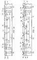
- FIGS. 3 a - 3 millustrate a process of forming a vertical interconnect structure with conductive pillars and a stress relief layer between a semiconductor die and build-up interconnect structure.
- a sacrificial or temporary substrate or carrier 120contains a base material such as silicon, polymer, polymer composite, metal foil, ceramic, glass, glass epoxy, beryllium oxide, tape, or other suitable low-cost, rigid material for structural support.
- An optional interface layer 122can be formed over carrier 120 as an etch-stop.
- An electrically conductive layer 124is formed over carrier 120 using patterning with PVD, CVD, sputtering, electrolytic plating, electroless plating process, or other suitable metal deposition process.
- Conductive layer 124can be one or more layers of Al, Cu, Sn, Ni, Au, Ag, W, poly-silicon, or other suitable electrically conductive material.
- Conductive layer 124includes wettable contact pads for later formation of conductive pillars. In one embodiment, the wettable contact pads of conductive layer 124 are pre-plated on carrier 120 .
- a plurality of conductive pillars or posts 128are formed over the wettable contact pads of conductive layer 124 .
- conductive pillars 128are formed by depositing one or more layers of photoresist over interface layer 122 or carrier 120 . The portion of photoresist over conductive layer 124 is exposed and removed by an etch development process. Conductive material is deposited in the removed portion of the photoresist layer using a selective plating process. The photoresist layer is stripped away leaving behind individual conductive pillars 128 .
- Conductive pillars 128can be Cu, Al, tungsten (W), Au, solder, or other suitable electrically conductive material.
- Conductive pillars 128have a height ranging from 2-120 micrometers ( ⁇ m). In another embodiment, conductive pillars 128 can be formed as stud bumps or stacked bumps.
- a plurality of semiconductor die or components 130is mounted to interface layer 122 with protective adhesive layer 132 in a flipchip arrangement.
- Contact pads 134 and active surface 136are oriented downward over interface layer 122 and carrier 120 .
- Protective adhesive layer 132can be one or more layers of ultraviolet (UV) curable and thermal stable adhesive tape.
- UVultraviolet
- Protective adhesive layer 132creates a vertical offset between active surface 136 and conductive layer 124 .
- Semiconductor die 130includes an active surface 136 containing analog or digital circuits implemented as active devices, passive devices, conductive layers, and dielectric layers formed within the die and electrically interconnected according to the electrical design and function of the die.
- the circuitmay include one or more transistors, diodes, and other circuit elements formed within active surface 136 to implement baseband analog circuits or digital circuits, such as digital signal processor (DSP), ASIC, memory, or other signal processing circuit.
- DSPdigital signal processor
- Semiconductor die 130may also contain IPD, such as inductors, capacitors, and resistors, for RF signal processing.
- a discrete semiconductor componentcan be mounted to interface layer 122 or carrier 120 .
- Conductive pillars 128are disposed around semiconductor die 130 .
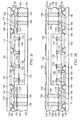
- FIG. 3 dshows an encapsulant or molding compound 138 deposited over semiconductor die 130 and conductive pillars 128 using a paste printing, compressive molding, transfer molding, liquid encapsulant molding, vacuum lamination, or other suitable applicator.
- Encapsulant 138can be polymer composite material, such as epoxy resin with filler, epoxy acrylate with filler, or polymer with proper filler.
- Encapsulant 138is non-conductive and environmentally protects the semiconductor device from external elements and contaminants.
- Protective adhesive layer 132prevents encapsulant 138 from bleeding into active surface 136 .
- carrier 120 , interface layer 122 , and protective adhesive layer 132are removed by chemical wet etching, plasma dry etching, mechanical peel-off, CMP, mechanical grinding, thermal bake, laser scanning, or wet stripping.
- Encapsulant 138provides structural support for semiconductor die 130 after removal of carrier 120 .
- Conductive layer 124 and contact pads 134 of semiconductor die 130are exposed following removal of carrier 120 , interface layer 122 , and protective adhesive layer 132 .
- the structureis inverted and a stress relief insulating layer 140 is formed over encapsulant 138 , conductive layer 124 , and active surface 136 using PVD, CVD, printing, spin coating, spray coating, sintering, or thermal oxidation.
- the stress relief insulating layer 140can be one or more layers of silicon dioxide (SiO2), silicon nitride (Si3N4), silicon oxynitride (SiON), tantalum pentoxide (Ta2O5), aluminum oxide (Al2O3), or other material having similar insulating and structural properties.
- the insulating layer 140is thicker over active region 136 , due to vertical offset of protective adhesive layer 132 , than over encapsulant 138 and conductive layer 124 to provide additional stress relief for semiconductor die 130 .
- the portion of insulating layer 140 over active region 136has a thickness ranging from 5-100 ⁇ m
- the portion of insulating layer 140 over encapsulant 138has a thickness ranging from 2-50 ⁇ m.
- a portion of insulating layer 140is removed by a patterning and etching process to expose conductive layer 124 and contact pads 134 , as shown in FIG. 3 g.
- a bottom-side build-up interconnect structure 142is formed over insulating layer 140 .
- An electrically conductive layer 144is formed over insulating layer 140 , conductive layer 124 , and contact pads 134 using patterning with PVD, CVD, sputtering, electrolytic plating, electroless plating process, or other suitable metal deposition process.
- Conductive layer 144can be one or more layers of Al, Cu, Sn, Ni, Au, Ag, or other suitable electrically conductive material. Portions of conductive layer 144 are electrically connected to conductive pillars 128 , conductive layer 124 , and contact pads 134 .
- portions of conductive layer 144can be electrically common or electrically isolated depending on the design and function of the semiconductor device.
- portion 145 of conductive layer 144operates as a redistribution layer (RDL) or runner to extend the conductivity of conductive pillars 128 and conductive layer 124 .
- RDLredistribution layer
- an insulating or passivation layer 146is formed over insulating layer 140 and conductive layer 144 using PVD, CVD, printing, spin coating, spray coating, sintering, or thermal oxidation.
- the passivation layer 146can be one or more layers of SiO2, Si3N4, SiON, Ta2O5, Al2O3, or other material having similar insulating and structural properties. A portion of passivation layer 146 is removed by an etching process to expose conductive layer 144 .
- An electrically conductive layer 148is formed over passivation layer 146 and conductive layer 144 using patterning with PVD, CVD, sputtering, electrolytic plating, electroless plating process, or other suitable metal deposition process.
- Conductive layer 148can be one or more layers of Al, Cu, Sn, Ni, Au, Ag, or other suitable electrically conductive material.
- Conductive layer 148is electrically connected to conductive layer 144 .
- Conductive layer 148is an under bump metallization (UBM) in electrical contact with conductive layer 144 and conductive pillars 128 .
- UBM 148can be a multi-metal stack with adhesion layer, barrier layer, and seed or wetting layer.
- the adhesion layeris formed over conductive layer 144 and can be Ti, titanium nitride (TiN), titanium tungsten (TiW), Al, or chromium (Cr).
- the barrier layeris formed over the adhesion layer and can be made of Ni, nickel vanadium (NiV), platinum (Pt), palladium (Pd), TiW, or chromium copper (CrCu).
- the barrier layerinhibits the diffusion of Cu into the active area of the die.
- the seed layercan be Cu, Ni, NiV, Au, or Al.
- the seed layeris formed over the barrier layer and acts as an intermediate conductive layer between conductive layer 144 and subsequent solder bumps or other interconnect structure.
- UBM 148provides a low resistive interconnect to conductive layer 144 , as well as a barrier to solder diffusion and seed layer for solder wettability.
- encapsulant 138undergoes grinding or plasma etching to planarize the surface for formation of the topside build-up interconnect structure.
- the grinding operationexposes a surface of conductive pillars 128 .
- An optional process carrier 150such as backgrinding tape, can be mounted to passivation layer 146 and conductive layer 148 with adhesive layer 152 for additional structural support during the grinding operation.
- the structureis inverted and a topside build-up interconnect structure 154 is formed over encapsulant 138 and conductive pillars 128 .
- An insulating or passivation layer 156is formed over encapsulant 138 and conductive pillars 128 using PVD, CVD, printing, spin coating, spray coating, sintering, or thermal oxidation.
- the passivation layer 156can be one or more layers of SiO2, Si3N4, SiON, Ta2O5, Al2O3, or other material having similar insulating and structural properties.
- a portion of passivation layer 156is removed by an etching process to expose conductive pillars 128 .
- An electrically conductive layer 158is formed over passivation layer 156 and conductive pillars 128 using patterning with PVD, CVD, sputtering, electrolytic plating, electroless plating process, or other suitable metal deposition process.
- Conductive layer 158can be one or more layers of Al, Cu, Sn, Ni, Au, Ag, or other suitable electrically conductive material.
- a portion of conductive layer 158is electrically connected to conductive pillars 128 .
- Other portions of conductive layer 158can be electrically common or electrically isolated depending on the design and function of the semiconductor device.
- portion 159 of conductive layer 158operates as an RDL or runner to extend the conductivity of conductive pillars 128 .
- an insulating or passivation layer 160is formed over passivation layer 156 and conductive layer 158 using PVD, CVD, printing, spin coating, spray coating, sintering, or thermal oxidation.
- the passivation layer 160can be one or more layers of SiO2, Si3N4, SiON, Ta2O5, Al2O3, or other material having similar insulating and structural properties. A portion of passivation layer 160 is removed by an etching process to expose conductive layer 158 .
- An electrically conductive layer 162is formed over passivation layer 160 and conductive layer 158 using patterning with PVD, CVD, sputtering, electrolytic plating, electroless plating process, or other suitable metal deposition process.
- Conductive layer 162can be one or more layers of Al, Cu, Sn, Ni, Au, Ag, or other suitable electrically conductive material.
- Conductive layer 162is a UBM in electrical contact with conductive layer 158 and conductive pillars 128 .
- UBM 162can be a multi-metal stack with adhesion layer, barrier layer, and seed or wetting layer.
- the adhesion layeris formed over conductive layer 158 and can be Ti, TiN, TiW, Al, or Cr.
- the barrier layeris formed over the adhesion layer and can be made of Ni, NiV, Pt, Pd, TiW, or CrCu.
- the barrier layerinhibits the diffusion of Cu into the active area of the die.
- the seed layercan be Cu, Ni, NiV, Au, or Al.
- the seed layeris formed over the barrier layer and acts as an intermediate conductive layer between conductive layer 158 and subsequent solder bumps or other interconnect structure.
- UBM 162provides a low resistive interconnect to conductive layer 158 , as well as a barrier to solder diffusion and seed layer for solder wettability.
- carrier 150 and adhesive layer 152is removed by chemical wet etching, plasma dry etching, mechanical peel-off, CMP, mechanical grinding, thermal bake, laser scanning, or wet stripping.
- the bottom-side build-up interconnect structure 142includes conductive layer 144 , passivation layer 146 , and UBM 148 .
- the topside build-up interconnect structure 154includes passivation layer 156 , conductive layer 158 , passivation layer 160 , and UBM 162 .
- An electrically conductive bump materialis deposited over UBM 148 using an evaporation, electrolytic plating, electroless plating, ball drop, or screen printing process.
- the bump materialcan be Al, Sn, Ni, Au, Ag, Pb, Bi, Cu, solder, and combinations thereof, with an optional flux solution.
- the bump materialcan be eutectic Sn/Pb, high-lead solder, or lead-free solder.
- the bump materialis bonded to UBM 148 using a suitable attachment or bonding process.
- the bump materialis reflowed by heating the material above its melting point to form spherical balls or bumps 164 .
- bumps 164are reflowed a second time to improve electrical contact to UBM 148 .
- the bumpscan also be compression bonded to UBM 148 .
- Bumps 164represent one type of interconnect structure that can be formed over UBM 148 .
- the interconnect structurecan also use bond wires, conductive paste, stud bump, micro bump, or other electrical interconnect.
- Conductive pillars 128provide vertical, z-direction interconnect between topside build-up interconnect layer 154 and bottom-side build-up interconnect layer 142 .
- Conductive layer 158is electrically connected through conductive pillars 128 to conductive layer 122 and contact pads 134 of each semiconductor device 168 .
- the thick protective insulating layer 140 disposed over active surface 136reduces stress caused by CTE mismatch between semiconductor die 130 and bottom-side build-up interconnect structure 142 .
- the stress buffering provided by insulating layer 140reduces joint failure rate of conductive pillars 138 and delamination between semiconductor die 130 and build-up interconnect structure 142 .
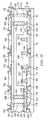
- FIG. 5shows a variation of the process flow of FIG. 3 j .
- Encapsulant 138 and conductive pillars 128undergo grinding or plasma etching to planarize the surface of the encapsulant for the topside build-up interconnect layer 154 .
- the grinding operationexposes a back surface of semiconductor die 130 coplanar with the exposed surface of conductive pillars 128 .
- the remainder of the processfollows the description of FIGS. 3 k - 3 m.
- FIG. 6illustrates an embodiment of the vertical interconnect structure with multiple IPD formed in the topside interconnect structure.
- semiconductor device 170uses a sacrificial or temporary substrate or carrier with an optional interface layer, which operates as an etch-stop layer.
- An electrically conductive layer 172is formed over the carrier using patterning with PVD, CVD, sputtering, electrolytic plating, electroless plating process, or other suitable metal deposition process.
- Conductive layer 172can be one or more layers of Al, Cu, Sn, Ni, Au, Ag, W, poly-silicon, or other suitable electrically conductive material.
- Conductive layer 172includes wettable contact pads for later formation of conductive pillars.
- a plurality of conductive pillars or posts 178is formed over the wettable contact pads of conductive layer 172 .
- conductive pillars 178are formed by depositing one or more layers of photoresist over the carrier and interface layer. The portion of photoresist over conductive layer 172 is exposed and removed by an etching development process. Conductive material is deposited in the removed portion of the photoresist layer using a selective plating process. The photoresist layer is stripped away leaving behind individual conductive pillars 178 .
- Conductive pillars 178can be Cu, Al, W, Au, solder, or other suitable electrically conductive material.
- Conductive pillars 178have a height ranging from 2-120 ⁇ m. In another embodiment, conductive pillars 178 can be formed as stud bumps or stacked bumps.
- a plurality of semiconductor die or components 180is mounted to the interface layer with a protective adhesive layer in a flipchip arrangement.
- Contact pads 184 and active surface 186are oriented downward over the interface layer and carrier.
- the protective adhesive layercan be one or more layers of UV curable and thermal stable adhesive tape.
- the protective adhesive layercreates a vertical offset between active surface 186 and conductive layer 172 .
- Semiconductor die 180includes an active surface 186 containing analog or digital circuits implemented as active devices, passive devices, conductive layers, and dielectric layers formed within the die and electrically interconnected according to the electrical design and function of the die.
- the circuitmay include one or more transistors, diodes, and other circuit elements formed within active surface 186 to implement baseband analog circuits or digital circuits, such as DSP, ASIC, memory, or other signal processing circuit.
- Semiconductor die 180may also contain IPD, such as inductors, capacitors, and resistors, for RF signal processing.
- IPDinductors, capacitors, and resistors
- a discrete semiconductor componentcan be mounted to the interface layer or carrier.
- An encapsulant or molding compound 188is deposited over semiconductor die 180 and conductive pillars 178 using a paste printing, compressive molding, transfer molding, liquid encapsulant molding, vacuum lamination, or other suitable applicator.
- Encapsulant 188can be polymer composite material, such as epoxy resin with filler, epoxy acrylate with filler, or polymer with proper filler.
- Encapsulant 188is non-conductive and environmentally protects the semiconductor device from external elements and contaminants.
- the carrier, interface layer, and protective adhesive layerare removed by chemical wet etching, plasma dry etching, mechanical peel-off, CMP, mechanical grinding, thermal bake, laser scanning, or wet stripping.
- Encapsulant 188provides structural support for semiconductor die 180 after removal of the carrier. Conductive layer 172 and contact pads 184 of semiconductor die 180 are exposed following removal of the carrier and interface layer.
- the structureis inverted and an insulating layer 190 is formed over encapsulant 188 , conductive layer 172 , and active surface 186 .
- the insulating layer 190is thicker over active region 186 , due to vertical offset of the protective adhesive layer, than over encapsulant 188 and conductive layer 172 .
- a portion of insulating layer 190is removed by a patterning and etching process to expose conductive layer 172 and contact pads 184 .
- a bottom-side build-up interconnect structure 192is formed over insulating layer 190 .
- the build-up interconnect structure 190includes an electrically conductive layer 194 , insulating or passivation layer 196 , and UBM 198 .
- Encapsulant 188undergoes grinding or plasma etching to planarize the surface for the topside build-up interconnect structure.
- the grinding operationexposes the top surface of conductive pillars 178 and, optionally, the back surface of semiconductor die 180 , as described in FIG. 5 .
- An optional process carriercan be mounted to passivation layer 196 and conductive layer 198 for additional structural support during the grinding operation.
- the structureis inverted and a topside build-up interconnect structure 200 is formed over encapsulant 188 and conductive pillars 178 .
- the build-up interconnect structure 200includes one or more IPDs.
- An insulating or passivation layer 202is formed over encapsulant 188 and conductive pillars 178 using spin coating, PVD, CVD, printing, sintering, or thermal oxidation.
- the passivation layer 202can be one or more layers of SiO2, Si3N4, SiON, Ta2O5, Al2O3, or other material having suitable insulating properties. A portion of passivation layer 202 is removed to expose conductive pillars 178 .
- An electrically conductive layer 204is formed over insulating layer 202 using patterning with PVD, CVD, sputtering, electrolytic plating, electroless plating process, or other suitable metal deposition process to form individual portions or sections.
- the individual portions of conductive layer 204can be electrically common or electrically isolated depending on the connectivity of the individual semiconductor die.
- Conductive layer 204can be one or more layers of Al, Cu, Sn, Ni, Au, Ag, or other suitable electrically conductive material.
- One portion of conductive layer 204is electrically connected to conductive pillars 178 .
- Other portions of conductive layer 204can be electrically common or electrically isolated depending on the design and function of the semiconductor device.
- a resistive layer 206 a - 206 bare patterned and deposited over conductive layer 204 and insulating layer 202 , respectively, using PVD or CVD.
- Resistive layer 206is tantalum silicide (TaxSiy) or other metal silicides, TaN, nickel chromium (NiCr), TiN, or doped poly-silicon having a resistivity between 5 and 100 ohm/sq.
- An insulating layer 208is formed over resistive layer 206 a using PVD, CVD, printing, sintering, or thermal oxidation.
- the insulating layer 208can be one or more layers of Si3N4, SiO2, SiON, Ta2O5, ZnO, ZrO2, Al2O3, polyimide, BCB, PBO, or other suitable dielectric material. Resistive layer 206 and insulating layer 208 can be formed with the same mask and etched at the same time. Alternatively, resistive layer 206 and insulating layer 208 can be patterned and etched with a different mask.
- An insulating or passivation layer 210is formed over passivation layer 202 , conductive layer 204 , resistive layer 206 , and insulating layer 208 using spin coating, PVD, CVD, printing, sintering, or thermal oxidation.
- the passivation layer 210can be one or more layers of SiO2, Si3N4, SiON, Ta2O5, Al2O3, or other material having suitable insulating properties. A portion of passivation layer 210 is removed to expose conductive layer 204 , resistive layer 206 , and insulating layer 208 .
- An electrically conductive layer 212is patterned and deposited over passivation layer 210 , conductive layer 204 , resistive layer 206 , and insulating layer 208 using PVD, CVD, sputtering, electrolytic plating, electroless plating process, or other suitable metal deposition process to form individual portions or sections for further interconnectivity.
- the individual portions of conductive layer 212can be electrically common or electrically isolated depending on the connectivity of the individual semiconductor die.
- Conductive layer 212can be one or more layers of Al, Cu, Sn, Ni, Au, Ag, or other suitable electrically conductive material.
- An insulating or passivation layer 214is formed over conductive layers 212 and passivation layer 210 using spin coating, PVD, CVD, printing, sintering, or thermal oxidation.
- the passivation layer 214can be one or more layers of SiO2, Si3N4, SiON, Ta2O5, Al2O3, or other material having suitable insulating properties. A portion of passivation layer 214 is removed to expose conductive layer 212 .
- An electrically conductive layer 216is patterned and deposited over passivation layer 214 and conductive layer 212 using PVD, CVD, sputtering, electrolytic plating, electroless plating process, or other suitable metal deposition process.
- Conductive layer 216can be one or more layers of Al, Cu, Sn, Ni, Au, Ag, or other suitable electrically conductive material.
- Conductive layer 216is a UBM in electrical contact with conductive layers 212 and 204 and conductive pillars 178 .
- conductive layer 204 , resistive layer 206 a , insulating layer 208 , and conductive layer 212is a metal-insulator-metal (MIM) capacitor.
- Resistive layer 206 bis a resistor element in the passive circuit.
- the individual sections of conductive layer 212can be wound or coiled in plan-view to produce or exhibit the desired properties of an inductor.
- the IPD structureprovides electrical characteristics needed for high frequency applications, such as resonators, high-pass filters, low-pass filters, band-pass filters, symmetric Hi-Q resonant transformers, matching networks, and tuning capacitors.
- the IPDscan be used as front-end wireless RF components, which can be positioned between the antenna and transceiver.
- the inductorcan be a hi-Q balun, transformer, or coil, operating up to 100 Gigahertz.
- multiple balunsare formed over a same substrate, allowing multi-band operation. For example, two or more baluns are used in a quad-band for mobile phones or other global system for mobile (GSM) communications, each balun dedicated for a frequency band of operation of the quad-band device.
- GSMglobal system for mobile
- a typical RF systemrequires multiple IPDs and other high frequency circuits in one or more semiconductor packages to perform the necessary electrical functions.
- the IPDscan be formed in either or both of the topside build-up interconnect structure and bottom-side build-up interconnect structure.
- the optional carrier and adhesive layer over passivation layer 196 and UBM 198are removed by chemical wet etching, plasma dry etching, mechanical peel-off, CMP, mechanical grinding, thermal bake, laser scanning, or wet stripping.
- An electrically conductive bump materialis deposited over UBM 198 using an evaporation, electrolytic plating, electroless plating, ball drop, or screen printing process.
- the bump materialcan be Al, Sn, Ni, Au, Ag, Pb, Bi, Cu, solder, and combinations thereof, with an optional flux solution.
- the bump materialcan be eutectic Sn/Pb, high-lead solder, or lead-free solder.
- the bump materialis bonded to UBM 198 using a suitable attachment or bonding process.
- the bump materialis reflowed by heating the material above its melting point to form spherical balls or bumps 218 .
- bumps 218are reflowed a second time to improve electrical contact to UBM 198 .
- the bumpscan also be compression bonded to UBM 198 .
- Bumps 218represent one type of interconnect structure that can be formed over UBM 198 .
- the interconnect structurecan also use bond wires, conductive paste, stud bump, micro bump, or other electrical interconnect.
- Conductive pillars 178provide vertical, z-direction interconnect between topside build-up interconnect layer 200 and bottom-side build-up interconnect layer 192 .
- Conductive layers 204 and 212are electrically connected through conductive pillars 178 to conductive layer 172 and contact pads 184 of semiconductor die 180 .
- the thick protective insulating layer 190 disposed over active surface 186reduces stress caused by CTE mismatch between semiconductor die 180 and bottom-side build-up interconnect structure 192 .
- the stress buffering provided by insulating layer 190reduces joint failure rate of conductive pillars 178 and delamination between semiconductor die 180 and build-up interconnect structure 192 .
Landscapes
- Engineering & Computer Science (AREA)
- Microelectronics & Electronic Packaging (AREA)
- Power Engineering (AREA)
- Computer Hardware Design (AREA)
- Physics & Mathematics (AREA)
- Condensed Matter Physics & Semiconductors (AREA)
- General Physics & Mathematics (AREA)
- Manufacturing & Machinery (AREA)
- Internal Circuitry In Semiconductor Integrated Circuit Devices (AREA)
Abstract
Description
Claims (25)
Priority Applications (4)
| Application Number | Priority Date | Filing Date | Title |
|---|---|---|---|
| US12/481,404US8039303B2 (en) | 2008-06-11 | 2009-06-09 | Method of forming stress relief layer between die and interconnect structure |
| TW099115255ATWI570820B (en) | 2009-06-09 | 2010-05-13 | Semiconductor device and method of forming stress relief layer between die and interconnect structure |
| US13/248,312US9006888B2 (en) | 2008-06-11 | 2011-09-29 | Semiconductor device and method of forming stress relief layer between die and interconnect structure |
| US14/637,054US10083916B2 (en) | 2008-06-11 | 2015-03-03 | Semiconductor device and method of forming stress relief layer between die and interconnect structure |
Applications Claiming Priority (2)
| Application Number | Priority Date | Filing Date | Title |
|---|---|---|---|
| US6077808P | 2008-06-11 | 2008-06-11 | |
| US12/481,404US8039303B2 (en) | 2008-06-11 | 2009-06-09 | Method of forming stress relief layer between die and interconnect structure |
Related Child Applications (1)
| Application Number | Title | Priority Date | Filing Date |
|---|---|---|---|
| US13/248,312DivisionUS9006888B2 (en) | 2008-06-11 | 2011-09-29 | Semiconductor device and method of forming stress relief layer between die and interconnect structure |
Publications (2)
| Publication Number | Publication Date |
|---|---|
| US20090309212A1 US20090309212A1 (en) | 2009-12-17 |
| US8039303B2true US8039303B2 (en) | 2011-10-18 |
Family
ID=41413977
Family Applications (3)
| Application Number | Title | Priority Date | Filing Date |
|---|---|---|---|
| US12/481,404Active2029-08-03US8039303B2 (en) | 2008-06-11 | 2009-06-09 | Method of forming stress relief layer between die and interconnect structure |
| US13/248,312Active2031-03-05US9006888B2 (en) | 2008-06-11 | 2011-09-29 | Semiconductor device and method of forming stress relief layer between die and interconnect structure |
| US14/637,054Active2030-01-01US10083916B2 (en) | 2008-06-11 | 2015-03-03 | Semiconductor device and method of forming stress relief layer between die and interconnect structure |
Family Applications After (2)
| Application Number | Title | Priority Date | Filing Date |
|---|---|---|---|
| US13/248,312Active2031-03-05US9006888B2 (en) | 2008-06-11 | 2011-09-29 | Semiconductor device and method of forming stress relief layer between die and interconnect structure |
| US14/637,054Active2030-01-01US10083916B2 (en) | 2008-06-11 | 2015-03-03 | Semiconductor device and method of forming stress relief layer between die and interconnect structure |
Country Status (1)
| Country | Link |
|---|---|
| US (3) | US8039303B2 (en) |
Cited By (54)
| Publication number | Priority date | Publication date | Assignee | Title |
|---|---|---|---|---|
| US20100244226A1 (en)* | 2009-03-24 | 2010-09-30 | James Sabatini | Stackable electronic package and method of fabricating same |
| US20110049695A1 (en)* | 2009-08-31 | 2011-03-03 | Stats Chippac, Ltd. | Semiconductor Device and Method of Forming Pre-Molded Semiconductor Die Having Bumps Embedded in Encapsulant |
| US20110241192A1 (en)* | 2010-04-02 | 2011-10-06 | Advanced Semiconductor Engineering, Inc. | Wafer-Level Semiconductor Device Packages with Stacking Functionality |
| US20110309492A1 (en)* | 2010-06-22 | 2011-12-22 | Chi Heejo | Integrated circuit system with recessed through silicon via pads and method of manufacture thereof |
| US20120112340A1 (en)* | 2007-12-14 | 2012-05-10 | Stats Chippac, Ltd. | Semiconductor Device and Method of Forming Insulating Layer Disposed Over The Semiconductor Die For Stress Relief |
| US20120190173A1 (en)* | 2011-01-20 | 2012-07-26 | Jia-Jin Tu | Method for packaging wafer |
| US8320134B2 (en) | 2010-02-05 | 2012-11-27 | Advanced Semiconductor Engineering, Inc. | Embedded component substrate and manufacturing methods thereof |
| US8358001B2 (en) | 2009-07-23 | 2013-01-22 | Advanced Semiconductor Engineering, Inc. | Semiconductor device packages, redistribution structures, and manufacturing methods thereof |
| US8372689B2 (en) | 2010-01-21 | 2013-02-12 | Advanced Semiconductor Engineering, Inc. | Wafer-level semiconductor device packages with three-dimensional fan-out and manufacturing methods thereof |
| US8378466B2 (en) | 2009-11-19 | 2013-02-19 | Advanced Semiconductor Engineering, Inc. | Wafer-level semiconductor device packages with electromagnetic interference shielding |
| US8405213B2 (en) | 2010-03-22 | 2013-03-26 | Advanced Semiconductor Engineering, Inc. | Semiconductor package including a stacking element |
| US8405212B2 (en) | 2009-12-31 | 2013-03-26 | Advanced Semiconductor Engineering, Inc. | Semiconductor package |
| US20130105966A1 (en)* | 2011-10-26 | 2013-05-02 | Maxim Integrated Products, Inc. | Three-dimensional chip-to-wafer integration |
| US20130119544A1 (en)* | 2010-06-29 | 2013-05-16 | Ravi K. Nalla | Microelectronic package and method of manufacturing same |
| US8569894B2 (en) | 2010-01-13 | 2013-10-29 | Advanced Semiconductor Engineering, Inc. | Semiconductor package with single sided substrate design and manufacturing methods thereof |
| US8569885B2 (en) | 2010-10-29 | 2013-10-29 | Advanced Semiconductor Engineering, Inc. | Stacked semiconductor packages and related methods |
| US8624374B2 (en) | 2010-04-02 | 2014-01-07 | Advanced Semiconductor Engineering, Inc. | Semiconductor device packages with fan-out and with connecting elements for stacking and manufacturing methods thereof |
| US8779564B1 (en)* | 2013-03-14 | 2014-07-15 | Intel IP Corporation | Semiconductor device with capacitive coupling structure |
| US20140197535A1 (en)* | 2012-05-18 | 2014-07-17 | Taiwan Semiconductor Manufacturing Company, Ltd. | Wafer-level packaging mechanisms |
| US8786100B2 (en) | 2010-03-15 | 2014-07-22 | Stats Chippac, Ltd. | Semiconductor device and method of forming repassivation layer with reduced opening to contact pad of semiconductor die |
| US20140203394A1 (en)* | 2013-01-23 | 2014-07-24 | United Microelectronics Corp. | Chip With Through Silicon Via Electrode And Method Of Forming The Same |
| US8823156B2 (en) | 2010-02-10 | 2014-09-02 | Advanced Semiconductor Engineering, Inc. | Semiconductor device packages having stacking functionality and including interposer |
| CN104051412A (en)* | 2013-03-14 | 2014-09-17 | 英特尔移动通信有限责任公司 | chip device |
| US8846454B2 (en) | 2007-12-14 | 2014-09-30 | Stats Chippac, Ltd. | Semiconductor device and method of forming interconnect structure for encapsulated die having pre-applied protective layer |
| US8907476B2 (en) | 2010-03-12 | 2014-12-09 | Stats Chippac, Ltd. | Semiconductor device and method of forming sacrificial protective layer to protect semiconductor die edge during singulation |
| US8941222B2 (en) | 2010-11-11 | 2015-01-27 | Advanced Semiconductor Engineering Inc. | Wafer level semiconductor package and manufacturing methods thereof |
| US20150255447A1 (en)* | 2013-03-06 | 2015-09-10 | Taiwan Semiconductor Manufacturing Company, Ltd. | Interconnect Structure for Package-on-Package Devices |
| US9171792B2 (en) | 2011-02-28 | 2015-10-27 | Advanced Semiconductor Engineering, Inc. | Semiconductor device packages having a side-by-side device arrangement and stacking functionality |
| US9202742B1 (en) | 2014-01-15 | 2015-12-01 | Stats Chippac Ltd. | Integrated circuit packaging system with pattern-through-mold and method of manufacture thereof |
| US9281297B2 (en) | 2014-03-07 | 2016-03-08 | Taiwan Semiconductor Manufacturing Company, Ltd. | Solution for reducing poor contact in info packages |
| US9293442B2 (en) | 2014-03-07 | 2016-03-22 | Taiwan Semiconductor Manufacturing Company, Ltd. | Semiconductor package and method |
| US20160099274A1 (en)* | 2014-10-07 | 2016-04-07 | Terapede Systems Inc. | 3d high resolution x-ray sensor with integrated scintillator grid |
| CN105489585A (en)* | 2014-10-09 | 2016-04-13 | 恒劲科技股份有限公司 | Packaging device and manufacturing method thereof |
| US9318441B2 (en) | 2007-12-14 | 2016-04-19 | Stats Chippac, Ltd. | Semiconductor device and method of forming sacrificial adhesive over contact pads of semiconductor die |
| US9355963B2 (en)* | 2014-09-26 | 2016-05-31 | Qualcomm Incorporated | Semiconductor package interconnections and method of making the same |
| US20160190099A1 (en)* | 2014-12-27 | 2016-06-30 | Siliconware Precision Industries Co., Ltd. | Package structure and fabrication method thereof |
| US9406658B2 (en) | 2010-12-17 | 2016-08-02 | Advanced Semiconductor Engineering, Inc. | Embedded component device and manufacturing methods thereof |
| US9449947B2 (en) | 2014-07-01 | 2016-09-20 | Taiwan Semiconductor Manufacturing Company, Ltd. | Semiconductor package for thermal dissipation |
| US9548240B2 (en) | 2010-03-15 | 2017-01-17 | STATS ChipPAC Pte. Ltd. | Semiconductor device and method of forming repassivation layer for robust low cost fan-out semiconductor package |
| US9564346B2 (en) | 2009-10-14 | 2017-02-07 | Advanced Semiconductor Engineering, Inc. | Package carrier, semiconductor package, and process for fabricating same |
| US9583420B2 (en) | 2015-01-23 | 2017-02-28 | Taiwan Semiconductor Manufacturing Company, Ltd. | Semiconductor device and method of manufactures |
| US9693455B1 (en)* | 2014-03-27 | 2017-06-27 | STATS ChipPAC Pte. Ltd. | Integrated circuit packaging system with plated copper posts and method of manufacture thereof |
| US9831148B2 (en)* | 2016-03-11 | 2017-11-28 | Taiwan Semiconductor Manufacturing Company, Ltd. | Integrated fan-out package including voltage regulators and methods forming same |
| US20180102298A1 (en)* | 2016-10-06 | 2018-04-12 | Mediatek Inc. | Semiconductor device |
| US20180233441A1 (en)* | 2013-01-29 | 2018-08-16 | Taiwan Semiconductor Manufacturing Company, Ltd. | PoP Device |
| US10147710B2 (en)* | 2014-09-18 | 2018-12-04 | Intel Corporation | Method of embedding WLCSP components in E-WLB and E-PLB |
| US10163851B2 (en) | 2015-11-30 | 2018-12-25 | Taiwan Semiconductor Manufacturing Company, Ltd. | Tri-layer CoWoS structure |
| TWI676248B (en)* | 2017-02-17 | 2019-11-01 | 聯發科技股份有限公司 | Semiconductor device |
| US10586780B2 (en)* | 2017-07-26 | 2020-03-10 | Micron Technology, Inc. | Semiconductor device modules including a die electrically connected to posts and related methods |
| TWI700805B (en)* | 2015-11-18 | 2020-08-01 | 美商艾馬克科技公司 | A semiconductor device with an electromagnetic interference (emi) shield |
| US11043446B2 (en)* | 2018-11-05 | 2021-06-22 | Samsung Electronics Co., Ltd. | Semiconductor package |
| US11101209B2 (en)* | 2017-09-29 | 2021-08-24 | Taiwan Semiconductor Manufacturing Company, Ltd. | Redistribution structures in semiconductor packages and methods of forming same |
| US11955434B2 (en) | 2015-12-22 | 2024-04-09 | Intel Corporation | Ultra small molded module integrated with die by module-on-wafer assembly |
| US20240128141A1 (en)* | 2022-10-14 | 2024-04-18 | Luxis Precision Intelligent Manufacturing (Kunshan) Co., Ltd. | Multi-chip packaging method and multi-chip packaging structure |
Families Citing this family (140)
| Publication number | Priority date | Publication date | Assignee | Title |
|---|---|---|---|---|
| TWI360207B (en) | 2007-10-22 | 2012-03-11 | Advanced Semiconductor Eng | Chip package structure and method of manufacturing |
| SG158823A1 (en) | 2008-07-18 | 2010-02-26 | United Test & Assembly Ct Ltd | Packaging structural member |
| US8183087B2 (en)* | 2008-09-09 | 2012-05-22 | Stats Chippac, Ltd. | Semiconductor device and method of forming a fan-out structure with integrated passive device and discrete component |
| US8114708B2 (en)* | 2008-09-30 | 2012-02-14 | General Electric Company | System and method for pre-patterned embedded chip build-up |
| KR101003678B1 (en)* | 2008-12-03 | 2010-12-23 | 삼성전기주식회사 | wafer level package and method of manufacturing the same and method for reusing chip |
| US9064936B2 (en) | 2008-12-12 | 2015-06-23 | Stats Chippac, Ltd. | Semiconductor device and method of forming a vertical interconnect structure for 3-D FO-WLCSP |
| US9293401B2 (en) | 2008-12-12 | 2016-03-22 | Stats Chippac, Ltd. | Semiconductor device and method for forming a low profile embedded wafer level ball grid array molded laser package (EWLP-MLP) |
| US7642128B1 (en) | 2008-12-12 | 2010-01-05 | Stats Chippac, Ltd. | Semiconductor device and method of forming a vertical interconnect structure for 3-D FO-WLCSP |
| US9082806B2 (en) | 2008-12-12 | 2015-07-14 | Stats Chippac, Ltd. | Semiconductor device and method of forming a vertical interconnect structure for 3-D FO-WLCSP |
| US7951663B2 (en)* | 2009-05-26 | 2011-05-31 | Stats Chippac, Ltd. | Semiconductor device and method of forming IPD structure using smooth conductive layer and bottom-side conductive layer |
| US9324672B2 (en)* | 2009-08-21 | 2016-04-26 | Stats Chippac, Ltd. | Semiconductor device and method of forming dual-active sided semiconductor die in fan-out wafer level chip scale package |
| US8883559B2 (en)* | 2009-09-25 | 2014-11-11 | Stats Chippac, Ltd. | Semiconductor device and method of forming adhesive material to secure semiconductor die to carrier in WLCSP |
| TWI497658B (en)* | 2009-10-07 | 2015-08-21 | Xintec Inc | Chip package and method of manufacturing same |
| US10283443B2 (en) | 2009-11-10 | 2019-05-07 | Taiwan Semiconductor Manufacturing Co., Ltd. | Chip package having integrated capacitor |
| US9941195B2 (en) | 2009-11-10 | 2018-04-10 | Taiwan Semiconductor Manufacturing Co., Ltd. | Vertical metal insulator metal capacitor |
| US9219023B2 (en)* | 2010-01-19 | 2015-12-22 | Globalfoundries Inc. | 3D chip stack having encapsulated chip-in-chip |
| US10297550B2 (en) | 2010-02-05 | 2019-05-21 | Taiwan Semiconductor Manufacturing Company, Ltd. | 3D IC architecture with interposer and interconnect structure for bonding dies |
| US8519537B2 (en) | 2010-02-26 | 2013-08-27 | Taiwan Semiconductor Manufacturing Company, Ltd. | 3D semiconductor package interposer with die cavity |
| US9385095B2 (en) | 2010-02-26 | 2016-07-05 | Taiwan Semiconductor Manufacturing Company, Ltd. | 3D semiconductor package interposer with die cavity |
| US8866301B2 (en)* | 2010-05-18 | 2014-10-21 | Taiwan Semiconductor Manufacturing Company, Ltd. | Package systems having interposers with interconnection structures |
| US9269691B2 (en) | 2010-05-26 | 2016-02-23 | Stats Chippac, Ltd. | Semiconductor device and method of making an embedded wafer level ball grid array (EWLB) package on package (POP) device with a slotted metal carrier interposer |
| US8349658B2 (en)* | 2010-05-26 | 2013-01-08 | Stats Chippac, Ltd. | Semiconductor device and method of forming conductive posts and heat sink over semiconductor die using leadframe |
| US8723299B2 (en) | 2010-06-01 | 2014-05-13 | Infineon Technologies Ag | Method and system for forming a thin semiconductor device |
| US10159154B2 (en)* | 2010-06-03 | 2018-12-18 | Hsio Technologies, Llc | Fusion bonded liquid crystal polymer circuit structure |
| US20130237055A1 (en)* | 2010-06-11 | 2013-09-12 | Imec | Method of redistributing functional element |
| JP5826532B2 (en)* | 2010-07-15 | 2015-12-02 | 新光電気工業株式会社 | Semiconductor device and manufacturing method thereof |
| US8669651B2 (en)* | 2010-07-26 | 2014-03-11 | Taiwan Semiconductor Manufacturing Company, Ltd. | Package-on-package structures with reduced bump bridging |
| TWI492349B (en)* | 2010-09-09 | 2015-07-11 | 矽品精密工業股份有限公司 | Chip scale package structure and fabrication method thereof |
| US8860079B2 (en) | 2010-11-15 | 2014-10-14 | United Test And Assembly Center Ltd. | Semiconductor packages and methods of packaging semiconductor devices |
| SG181248A1 (en)* | 2010-11-15 | 2012-06-28 | United Test & Assembly Ct Lt | Semiconductor packages and methods of packaging semiconductor devices |
| US8804339B2 (en)* | 2011-02-28 | 2014-08-12 | Toyota Motor Engineering & Manufacturing North America, Inc. | Power electronics assemblies, insulated metal substrate assemblies, and vehicles incorporating the same |
| TWI441292B (en)* | 2011-03-02 | 2014-06-11 | 矽品精密工業股份有限公司 | Semiconductor structure and fabrication method thereof |
| US8654541B2 (en) | 2011-03-24 | 2014-02-18 | Toyota Motor Engineering & Manufacturing North America, Inc. | Three-dimensional power electronics packages |
| US20130049214A1 (en)* | 2011-08-29 | 2013-02-28 | Infineon Technologies Ag | Method of processing at least one die and die arrangement |
| US9679863B2 (en)* | 2011-09-23 | 2017-06-13 | STATS ChipPAC Pte. Ltd. | Semiconductor device and method of forming interconnect substrate for FO-WLCSP |
| US9123763B2 (en) | 2011-10-12 | 2015-09-01 | Taiwan Semiconductor Manufacturing Company, Ltd. | Package-on-package (PoP) structure having at least one package comprising one die being disposed in a core material between first and second surfaces of the core material |
| US8975741B2 (en) | 2011-10-17 | 2015-03-10 | Taiwan Semiconductor Manufacturing Company, Ltd. | Process for forming package-on-package structures |
| KR101532816B1 (en)* | 2011-11-14 | 2015-06-30 | 유나이티드 테스트 엔드 어셈블리 센터 엘티디 | Semiconductor packages and methods of packaging semiconductor devices |
| US10050004B2 (en)* | 2015-11-20 | 2018-08-14 | Deca Technologies Inc. | Fully molded peripheral package on package device |
| US8518796B2 (en) | 2012-01-09 | 2013-08-27 | Taiwan Semiconductor Manufacturing Company, Ltd. | Semiconductor die connection system and method |
| US9412689B2 (en)* | 2012-01-24 | 2016-08-09 | Taiwan Semiconductor Manufacturing Company, Ltd. | Semiconductor packaging structure and method |
| US9799589B2 (en)* | 2012-03-23 | 2017-10-24 | STATS ChipPAC Pte. Ltd. | Integrated circuit packaging system with a grid array with a leadframe and method of manufacture thereof |
| US8658473B2 (en)* | 2012-03-27 | 2014-02-25 | General Electric Company | Ultrathin buried die module and method of manufacturing thereof |
| JP2013236039A (en)* | 2012-05-11 | 2013-11-21 | Renesas Electronics Corp | Semiconductor device |
| US9960106B2 (en) | 2012-05-18 | 2018-05-01 | Taiwan Semiconductor Manufacturing Co., Ltd. | Package with metal-insulator-metal capacitor and method of manufacturing the same |
| KR101947722B1 (en)* | 2012-06-07 | 2019-04-25 | 삼성전자주식회사 | stack semiconductor package and method of manufacturing the same |
| US9443783B2 (en) | 2012-06-27 | 2016-09-13 | Taiwan Semiconductor Manufacturing Company, Ltd. | 3DIC stacking device and method of manufacture |
| US8669655B2 (en)* | 2012-08-02 | 2014-03-11 | Infineon Technologies Ag | Chip package and a method for manufacturing a chip package |
| TWI485815B (en)* | 2012-08-10 | 2015-05-21 | 矽品精密工業股份有限公司 | Semiconductor package and method of fabricating the same |
| US9818734B2 (en) | 2012-09-14 | 2017-11-14 | STATS ChipPAC Pte. Ltd. | Semiconductor device and method of forming build-up interconnect structures over a temporary substrate |
| US9385052B2 (en) | 2012-09-14 | 2016-07-05 | STATS ChipPAC Pte. Ltd. | Semiconductor device and method of forming build-up interconnect structures over carrier for testing at interim stages |
| US9245804B2 (en)* | 2012-10-23 | 2016-01-26 | Nxp B.V. | Using a double-cut for mechanical protection of a wafer-level chip scale package (WLCSP) |
| US9312193B2 (en)* | 2012-11-09 | 2016-04-12 | Taiwan Semiconductor Manufacturing Company, Ltd. | Stress relief structures in package assemblies |
| US9508674B2 (en)* | 2012-11-14 | 2016-11-29 | Taiwan Semiconductor Manufacturing Company, Ltd. | Warpage control of semiconductor die package |
| CN103906371B (en)* | 2012-12-27 | 2017-09-19 | 碁鼎科技秦皇岛有限公司 | Circuit board with embedded element and preparation method thereof |
| US20140225248A1 (en)* | 2013-02-13 | 2014-08-14 | Qualcomm Incorporated | Power distribution and thermal solution for direct stacked integrated circuits |
| US9685350B2 (en)* | 2013-03-08 | 2017-06-20 | STATS ChipPAC, Pte. Ltd. | Semiconductor device and method of forming embedded conductive layer for power/ground planes in Fo-eWLB |
| US9087832B2 (en)* | 2013-03-08 | 2015-07-21 | Taiwan Semiconductor Manufacturing Company, Ltd. | Warpage reduction and adhesion improvement of semiconductor die package |
| CN104037124B (en)* | 2013-03-08 | 2019-03-26 | 新科金朋有限公司 | Form the semiconductor devices and method for the insertion conductive layer of power ground plane in FO-EWLB |
| US9214423B2 (en)* | 2013-03-15 | 2015-12-15 | Semiconductor Components Industries, Llc | Method of forming a HEMT semiconductor device and structure therefor |
| KR20140126598A (en)* | 2013-04-23 | 2014-10-31 | 삼성전자주식회사 | semiconductor package and method for manufacturing of the same |
| US9406533B2 (en) | 2013-06-27 | 2016-08-02 | STATS ChipPAC Pte. Ltd. | Methods of forming conductive and insulating layers |
| US10667410B2 (en) | 2013-07-11 | 2020-05-26 | Hsio Technologies, Llc | Method of making a fusion bonded circuit structure |
| US9543373B2 (en)* | 2013-10-23 | 2017-01-10 | Taiwan Semiconductor Manufacturing Company, Ltd. | Semiconductor structure and manufacturing method thereof |
| US9324780B2 (en)* | 2013-11-01 | 2016-04-26 | Taiwan Semiconductor Manufacturing Co., Ltd. | Metal-insulator-metal (MIM) capacitor structure including redistribution layer |
| US9129981B2 (en)* | 2013-11-26 | 2015-09-08 | Freescale Semiconductor Inc. | Methods for the production of microelectronic packages having radiofrequency stand-off layers |
| US9653442B2 (en) | 2014-01-17 | 2017-05-16 | Taiwan Semiconductor Manufacturing Company, Ltd. | Integrated circuit package and methods of forming same |
| US9252110B2 (en) | 2014-01-17 | 2016-02-02 | Taiwan Semiconductor Manufacturing Company, Ltd. | Interconnect structure and method of forming same |
| US9577025B2 (en)* | 2014-01-31 | 2017-02-21 | Qualcomm Incorporated | Metal-insulator-metal (MIM) capacitor in redistribution layer (RDL) of an integrated device |
| US9768090B2 (en) | 2014-02-14 | 2017-09-19 | Taiwan Semiconductor Manufacturing Company, Ltd. | Substrate design for semiconductor packages and method of forming same |
| US9653443B2 (en) | 2014-02-14 | 2017-05-16 | Taiwan Semiconductor Manufacturing Company, Ltd. | Thermal performance structure for semiconductor packages and method of forming same |
| US10026671B2 (en) | 2014-02-14 | 2018-07-17 | Taiwan Semiconductor Manufacturing Company, Ltd. | Substrate design for semiconductor packages and method of forming same |
| US9935090B2 (en) | 2014-02-14 | 2018-04-03 | Taiwan Semiconductor Manufacturing Company, Ltd. | Substrate design for semiconductor packages and method of forming same |
| US10056267B2 (en) | 2014-02-14 | 2018-08-21 | Taiwan Semiconductor Manufacturing Company, Ltd. | Substrate design for semiconductor packages and method of forming same |
| US9263302B2 (en) | 2014-02-21 | 2016-02-16 | Taiwan Semiconductor Manufacturing Company, Ltd. | Via structure for packaging and a method of forming |
| US9502355B2 (en)* | 2014-02-26 | 2016-11-22 | Nvidia Corporation | Bottom package having routing paths connected to top package and method of manufacturing the same |
| US9397138B2 (en)* | 2014-03-25 | 2016-07-19 | Xintec Inc. | Manufacturing method of semiconductor structure |
| US9929126B2 (en) | 2014-04-03 | 2018-03-27 | Taiwan Semiconductor Manufacturing Company, Ltd. | Packages with metal line crack prevention design |
| TW201543641A (en) | 2014-05-12 | 2015-11-16 | Xintex Inc | Chip package and method of manufacturing same |
| US9831214B2 (en)* | 2014-06-18 | 2017-11-28 | Taiwan Semiconductor Manufacturing Company, Ltd. | Semiconductor device packages, packaging methods, and packaged semiconductor devices |
| US10177032B2 (en)* | 2014-06-18 | 2019-01-08 | Taiwan Semiconductor Manufacturing Company, Ltd. | Devices, packaging devices, and methods of packaging semiconductor devices |
| TWI584430B (en)* | 2014-09-10 | 2017-05-21 | 矽品精密工業股份有限公司 | Semiconductor package and manufacturing method thereof |
| KR20160047424A (en) | 2014-09-26 | 2016-05-02 | 인텔 코포레이션 | Integrated circuit package having wire-bonded multi-die stack |
| US9318442B1 (en)* | 2014-09-29 | 2016-04-19 | Taiwan Semiconductor Manufacturing Company, Ltd. | Integrated fan-out package with dummy vias |
| US10468381B2 (en) | 2014-09-29 | 2019-11-05 | Apple Inc. | Wafer level integration of passive devices |
| TWI552282B (en)* | 2014-11-03 | 2016-10-01 | 矽品精密工業股份有限公司 | Package structure and manufacturing method thereof |
| US9564416B2 (en) | 2015-02-13 | 2017-02-07 | Taiwan Semiconductor Manufacturing Company, Ltd. | Package structures and methods of forming the same |
| US10032704B2 (en) | 2015-02-13 | 2018-07-24 | Taiwan Semiconductor Manufacturing Company, Ltd. | Reducing cracking by adjusting opening size in pop packages |
| US9704836B2 (en) | 2015-03-16 | 2017-07-11 | Mediatek Inc. | Semiconductor package assembly |
| TWI597809B (en)* | 2015-03-23 | 2017-09-01 | 矽品精密工業股份有限公司 | Electronic package and the manufacture thereof |
| US10128207B2 (en)* | 2015-03-31 | 2018-11-13 | Stmicroelectronics Pte Ltd | Semiconductor packages with pillar and bump structures |
| US9893017B2 (en) | 2015-04-09 | 2018-02-13 | STATS ChipPAC Pte. Ltd. | Double-sided semiconductor package and dual-mold method of making same |
| KR101651362B1 (en)* | 2015-05-22 | 2016-08-25 | 앰코 테크놀로지 코리아 주식회사 | Method for fabricating semiconductor package and semiconductor package using the same |
| US9761540B2 (en)* | 2015-06-24 | 2017-09-12 | Micron Technology, Inc. | Wafer level package and fabrication method thereof |
| US10276541B2 (en)* | 2015-06-30 | 2019-04-30 | Taiwan Semiconductor Manufacturing Company, Ltd. | 3D package structure and methods of forming same |
| US20170011934A1 (en)* | 2015-07-10 | 2017-01-12 | Dyi-chung Hu | Fabricating process for redistribution layer |
| US9786599B2 (en) | 2015-08-21 | 2017-10-10 | Taiwan Semiconductor Manufacturing Company, Ltd. | Package structures and method of forming the same |
| KR102372300B1 (en)* | 2015-11-26 | 2022-03-08 | 삼성전자주식회사 | Stacked package and method of manufacturing the same |
| US20190206833A1 (en)* | 2015-12-23 | 2019-07-04 | Intel IP Corporation | Eplb/ewlb based pop for hbm or customized package stack |
| US9842815B2 (en) | 2016-02-26 | 2017-12-12 | Taiwan Semiconductor Manufacturing Company, Ltd. | Semiconductor device and method of manufacture |
| US10204870B2 (en)* | 2016-04-28 | 2019-02-12 | Taiwan Semiconductor Manufacturing Co., Ltd. | Semiconductor device and method of manufacturing the same |
| US10297575B2 (en) | 2016-05-06 | 2019-05-21 | Amkor Technology, Inc. | Semiconductor device utilizing an adhesive to attach an upper package to a lower die |
| US20170338204A1 (en) | 2016-05-17 | 2017-11-23 | Taiwan Semiconductor Manufacturing Company, Ltd. | Device and Method for UBM/RDL Routing |
| US10770795B2 (en) | 2016-05-27 | 2020-09-08 | Taiwan Semiconductor Manufacturing Co., Ltd. | Antenna device and method for manufacturing antenna device |
| US9812414B1 (en)* | 2016-06-17 | 2017-11-07 | Nanya Technology Corporation | Chip package and a manufacturing method thereof |
| US20170365567A1 (en)* | 2016-06-20 | 2017-12-21 | Samsung Electro-Mechanics Co., Ltd. | Fan-out semiconductor package |
| US10600748B2 (en) | 2016-06-20 | 2020-03-24 | Samsung Electronics Co., Ltd. | Fan-out semiconductor package |
| US10276506B2 (en)* | 2016-07-21 | 2019-04-30 | Taiwan Semiconductor Manufacturing Co., Ltd. | Integrated fan-out package |
| US9997471B2 (en) | 2016-07-25 | 2018-06-12 | Taiwan Semiconductor Manufacturing Company Ltd. | Semiconductor package structure and manufacturing method thereof |
| KR101982044B1 (en)* | 2016-08-31 | 2019-05-24 | 삼성전기주식회사 | Fan-out semiconductor package |
| KR101973431B1 (en)* | 2016-09-29 | 2019-04-29 | 삼성전기주식회사 | Fan-out semiconductor package |
| US20190259731A1 (en)* | 2016-11-09 | 2019-08-22 | Unisem (M) Berhad | Substrate based fan-out wafer level packaging |
| US10366953B2 (en) | 2016-12-05 | 2019-07-30 | Taiwan Semiconductor Manufacturing Co., Ltd. | Redistribution layer structures for integrated circuit package |
| US10574198B2 (en)* | 2016-12-22 | 2020-02-25 | Nxp Usa, Inc. | Integrated circuit devices with selectively arranged through substrate vias and method of manufacture thereof |
| KR102055593B1 (en)* | 2017-02-03 | 2019-12-13 | 삼성전자주식회사 | Fan-out semiconductor package |
| US9972581B1 (en)* | 2017-02-07 | 2018-05-15 | Taiwan Semiconductor Manufacturing Company, Ltd. | Routing design of dummy metal cap and redistribution line |
| US10784220B2 (en) | 2017-03-30 | 2020-09-22 | Taiwan Semiconductor Manufacturing Co., Ltd. | Plurality of semiconductor devices encapsulated by a molding material attached to a redistribution layer |
| US10468345B2 (en)* | 2017-05-19 | 2019-11-05 | Taiwan Semiconductor Manufacturing Company Ltd. | 3D IC decoupling capacitor structure and method for manufacturing the same |
| DE102017126028B4 (en) | 2017-06-30 | 2020-12-10 | Taiwan Semiconductor Manufacturing Co., Ltd. | Housing and manufacturing method using a release film as an insulating film |
| US10170341B1 (en) | 2017-06-30 | 2019-01-01 | Taiwan Semiconductor Manufacturing Company, Ltd. | Release film as isolation film in package |
| US10777515B2 (en)* | 2017-10-25 | 2020-09-15 | Sj Semiconductor (Jiangyin) Corporation | Fan-out antenna packaging structure and preparation method thereof |
| KR101963293B1 (en) | 2017-11-01 | 2019-03-28 | 삼성전기주식회사 | Fan-out semiconductor package |
| US10553533B2 (en)* | 2017-11-08 | 2020-02-04 | Taiwan Semiconductor Manufacturing Co., Ltd. | Integrated fan-out package and manufacturing method thereof |
| EP3483921A1 (en)* | 2017-11-11 | 2019-05-15 | AT & S Austria Technologie & Systemtechnik Aktiengesellschaft | Embedding known-good component in known-good cavity of known-good component carrier material with pre-formed electric connection structure |
| US10797005B2 (en)* | 2017-11-27 | 2020-10-06 | Taiwan Semiconductor Manufacturing Company Ltd. | Semiconductor package and method for manufacturing the same |
| US10510634B2 (en) | 2017-11-30 | 2019-12-17 | Taiwan Semiconductor Manufacturing Company, Ltd. | Package structure and method |
| KR101933425B1 (en)* | 2017-11-30 | 2018-12-28 | 삼성전기 주식회사 | Semiconductor package |
| US10773381B2 (en)* | 2017-11-30 | 2020-09-15 | Skygrid, Llc | Secure distributed system using blockchain for self-policing of autonomous agents |
| JP2019149507A (en)* | 2018-02-28 | 2019-09-05 | 東芝メモリ株式会社 | Semiconductor device and manufacturing method thereof |
| US11063007B2 (en)* | 2018-05-21 | 2021-07-13 | Taiwan Semiconductor Manufacturing Company, Ltd. | Semiconductor device and method of manufacture |
| KR102653212B1 (en)* | 2018-11-26 | 2024-04-01 | 삼성전기주식회사 | Semiconductor package |
| US11088095B2 (en)* | 2018-12-07 | 2021-08-10 | Nanya Technology Corporation | Package structure |
| US10950551B2 (en)* | 2019-04-29 | 2021-03-16 | Advanced Semiconductor Engineering, Inc. | Embedded component package structure and manufacturing method thereof |
| US11309285B2 (en)* | 2019-06-13 | 2022-04-19 | Micron Technology, Inc. | Three-dimensional stacking semiconductor assemblies and methods of manufacturing the same |
| US11088079B2 (en)* | 2019-06-27 | 2021-08-10 | Taiwan Semiconductor Manufacturing Co., Ltd. | Package structure having line connected via portions |
| US11094620B2 (en)* | 2019-09-30 | 2021-08-17 | Texas Instruments Incorporated | Integrated capacitor with extended head bump bond pillar |
| KR20220033636A (en)* | 2020-09-09 | 2022-03-17 | 삼성전자주식회사 | Semiconductor package |
| KR20220109753A (en) | 2021-01-29 | 2022-08-05 | 삼성전자주식회사 | Semiconductor package including a post |
| US20220270909A1 (en)* | 2021-02-25 | 2022-08-25 | Marvell Asia Pte Ltd | Glass carrier stacked package assembly method |
| FR3125357A1 (en)* | 2021-07-16 | 2023-01-20 | Stmicroelectronics (Tours) Sas | Process for manufacturing electronic chips |
Citations (9)
| Publication number | Priority date | Publication date | Assignee | Title |
|---|---|---|---|---|
| US6028364A (en) | 1994-09-20 | 2000-02-22 | Hitachi, Ltd. | Semiconductor device having a stress relieving mechanism |
| US6197613B1 (en) | 1999-03-23 | 2001-03-06 | Industrial Technology Research Institute | Wafer level packaging method and devices formed |
| US6423571B2 (en) | 1994-09-20 | 2002-07-23 | Hitachi, Ltd. | Method of making a semiconductor device having a stress relieving mechanism |
| US20040080025A1 (en)* | 2002-09-17 | 2004-04-29 | Shinko Electric Industries Co., Ltd. | Lead frame, method of manufacturing the same, and semiconductor device manufactured with the same |
| US20050006737A1 (en)* | 2002-04-29 | 2005-01-13 | Shafidul Islam | Partially patterned lead frames and methods of making and using the same in semiconductor packaging |
| US6946325B2 (en)* | 2003-03-14 | 2005-09-20 | Micron Technology, Inc. | Methods for packaging microelectronic devices |
| US7192807B1 (en) | 2002-11-08 | 2007-03-20 | Amkor Technology, Inc. | Wafer level package and fabrication method |
| US20080029890A1 (en)* | 2006-08-03 | 2008-02-07 | Unimicron Technology Corp. | Embedded chip package process and circuit board with embedded chip |
| US20090206461A1 (en)* | 2008-02-15 | 2009-08-20 | Qimonda Ag | Integrated circuit and method |
Family Cites Families (14)
| Publication number | Priority date | Publication date | Assignee | Title |
|---|---|---|---|---|
| US5250843A (en) | 1991-03-27 | 1993-10-05 | Integrated System Assemblies Corp. | Multichip integrated circuit modules |
| US5353498A (en) | 1993-02-08 | 1994-10-11 | General Electric Company | Method for fabricating an integrated circuit module |
| US5841193A (en) | 1996-05-20 | 1998-11-24 | Epic Technologies, Inc. | Single chip modules, repairable multichip modules, and methods of fabrication thereof |
| KR100495921B1 (en) | 2002-12-30 | 2005-06-17 | 주식회사 하이닉스반도체 | Method of fabrication semiconductor device for remove stress |
| TWI244167B (en) | 2003-11-10 | 2005-11-21 | Siliconware Precision Industries Co Ltd | Semiconductor package and method thereof |
| US7244634B2 (en)* | 2004-03-31 | 2007-07-17 | Intel Corporation | Stress-relief layer and stress-compensation collar in contact arrays, and processes of making same |
| US7368379B2 (en) | 2005-08-04 | 2008-05-06 | Taiwan Semiconductor Manufacturing Company, Ltd. | Multi-layer interconnect structure for semiconductor devices |
| US8072059B2 (en) | 2006-04-19 | 2011-12-06 | Stats Chippac, Ltd. | Semiconductor device and method of forming UBM fixed relative to interconnect structure for alignment of semiconductor die |
| KR101037229B1 (en)* | 2006-04-27 | 2011-05-25 | 스미토모 베이클리트 컴퍼니 리미티드 | Semiconductor device and manufacturing method of semiconductor device |
| US7713782B2 (en) | 2006-09-22 | 2010-05-11 | Stats Chippac, Inc. | Fusible I/O interconnection systems and methods for flip-chip packaging involving substrate-mounted stud-bumps |
| US8193034B2 (en) | 2006-11-10 | 2012-06-05 | Stats Chippac, Ltd. | Semiconductor device and method of forming vertical interconnect structure using stud bumps |
| US8174119B2 (en) | 2006-11-10 | 2012-05-08 | Stats Chippac, Ltd. | Semiconductor package with embedded die |
| US20080273410A1 (en)* | 2007-05-04 | 2008-11-06 | Jaydeb Goswami | Tungsten digitlines |
| US7868445B2 (en) | 2007-06-25 | 2011-01-11 | Epic Technologies, Inc. | Integrated structures and methods of fabrication thereof with fan-out metallization on a chips-first chip layer |
- 2009
- 2009-06-09USUS12/481,404patent/US8039303B2/enactiveActive
- 2011
- 2011-09-29USUS13/248,312patent/US9006888B2/enactiveActive
- 2015
- 2015-03-03USUS14/637,054patent/US10083916B2/enactiveActive
Patent Citations (9)
| Publication number | Priority date | Publication date | Assignee | Title |
|---|---|---|---|---|
| US6028364A (en) | 1994-09-20 | 2000-02-22 | Hitachi, Ltd. | Semiconductor device having a stress relieving mechanism |
| US6423571B2 (en) | 1994-09-20 | 2002-07-23 | Hitachi, Ltd. | Method of making a semiconductor device having a stress relieving mechanism |
| US6197613B1 (en) | 1999-03-23 | 2001-03-06 | Industrial Technology Research Institute | Wafer level packaging method and devices formed |
| US20050006737A1 (en)* | 2002-04-29 | 2005-01-13 | Shafidul Islam | Partially patterned lead frames and methods of making and using the same in semiconductor packaging |
| US20040080025A1 (en)* | 2002-09-17 | 2004-04-29 | Shinko Electric Industries Co., Ltd. | Lead frame, method of manufacturing the same, and semiconductor device manufactured with the same |
| US7192807B1 (en) | 2002-11-08 | 2007-03-20 | Amkor Technology, Inc. | Wafer level package and fabrication method |
| US6946325B2 (en)* | 2003-03-14 | 2005-09-20 | Micron Technology, Inc. | Methods for packaging microelectronic devices |
| US20080029890A1 (en)* | 2006-08-03 | 2008-02-07 | Unimicron Technology Corp. | Embedded chip package process and circuit board with embedded chip |
| US20090206461A1 (en)* | 2008-02-15 | 2009-08-20 | Qimonda Ag | Integrated circuit and method |
Cited By (109)
| Publication number | Priority date | Publication date | Assignee | Title |
|---|---|---|---|---|
| US8456002B2 (en)* | 2007-12-14 | 2013-06-04 | Stats Chippac Ltd. | Semiconductor device and method of forming insulating layer disposed over the semiconductor die for stress relief |
| US9559029B2 (en) | 2007-12-14 | 2017-01-31 | STATS ChipPAC Pte. Ltd. | Semiconductor device and method of forming interconnect structure for encapsulated die having pre-applied protective layer |
| US9318441B2 (en) | 2007-12-14 | 2016-04-19 | Stats Chippac, Ltd. | Semiconductor device and method of forming sacrificial adhesive over contact pads of semiconductor die |
| US9666500B2 (en) | 2007-12-14 | 2017-05-30 | STATS ChipPAC Pte. Ltd. | Semiconductor device and method of forming insulating layer disposed over the semiconductor die for stress relief |
| US20120112340A1 (en)* | 2007-12-14 | 2012-05-10 | Stats Chippac, Ltd. | Semiconductor Device and Method of Forming Insulating Layer Disposed Over The Semiconductor Die For Stress Relief |
| US9252066B2 (en) | 2007-12-14 | 2016-02-02 | Stats Chippac, Ltd. | Semiconductor device and method of forming interconnect structure for encapsulated die having pre-applied protective layer |
| US8846454B2 (en) | 2007-12-14 | 2014-09-30 | Stats Chippac, Ltd. | Semiconductor device and method of forming interconnect structure for encapsulated die having pre-applied protective layer |
| US10998248B2 (en) | 2007-12-14 | 2021-05-04 | JCET Semiconductor (Shaoxing) Co. Ltd. | Semiconductor device and method of forming sacrificial adhesive over contact pads of semiconductor die |
| US8759155B2 (en) | 2007-12-14 | 2014-06-24 | Stats Chippac, Ltd. | Semiconductor device and method of forming insulating layer disposed over the semiconductor die for stress relief |
| US10014286B2 (en)* | 2009-03-24 | 2018-07-03 | General Electric Company | Stackable electronics package and method of fabricating same |
| US20100244226A1 (en)* | 2009-03-24 | 2010-09-30 | James Sabatini | Stackable electronic package and method of fabricating same |
| US11309304B2 (en) | 2009-03-24 | 2022-04-19 | General Electric Company | Stackable electronic package and method of fabricating same |
| US8358001B2 (en) | 2009-07-23 | 2013-01-22 | Advanced Semiconductor Engineering, Inc. | Semiconductor device packages, redistribution structures, and manufacturing methods thereof |
| US9397050B2 (en) | 2009-08-31 | 2016-07-19 | STATS ChipPAC Pte. Ltd. | Semiconductor device and method of forming pre-molded semiconductor die having bumps embedded in encapsulant |
| US20110049695A1 (en)* | 2009-08-31 | 2011-03-03 | Stats Chippac, Ltd. | Semiconductor Device and Method of Forming Pre-Molded Semiconductor Die Having Bumps Embedded in Encapsulant |
| US9564346B2 (en) | 2009-10-14 | 2017-02-07 | Advanced Semiconductor Engineering, Inc. | Package carrier, semiconductor package, and process for fabricating same |
| US8378466B2 (en) | 2009-11-19 | 2013-02-19 | Advanced Semiconductor Engineering, Inc. | Wafer-level semiconductor device packages with electromagnetic interference shielding |
| US8405212B2 (en) | 2009-12-31 | 2013-03-26 | Advanced Semiconductor Engineering, Inc. | Semiconductor package |
| US8569894B2 (en) | 2010-01-13 | 2013-10-29 | Advanced Semiconductor Engineering, Inc. | Semiconductor package with single sided substrate design and manufacturing methods thereof |
| US8884424B2 (en) | 2010-01-13 | 2014-11-11 | Advanced Semiconductor Engineering, Inc. | Semiconductor package with single sided substrate design and manufacturing methods thereof |
| US9196597B2 (en) | 2010-01-13 | 2015-11-24 | Advanced Semiconductor Engineering, Inc. | Semiconductor package with single sided substrate design and manufacturing methods thereof |
| US8372689B2 (en) | 2010-01-21 | 2013-02-12 | Advanced Semiconductor Engineering, Inc. | Wafer-level semiconductor device packages with three-dimensional fan-out and manufacturing methods thereof |
| US8320134B2 (en) | 2010-02-05 | 2012-11-27 | Advanced Semiconductor Engineering, Inc. | Embedded component substrate and manufacturing methods thereof |
| US8823156B2 (en) | 2010-02-10 | 2014-09-02 | Advanced Semiconductor Engineering, Inc. | Semiconductor device packages having stacking functionality and including interposer |
| US9558958B2 (en) | 2010-03-12 | 2017-01-31 | STATS ChipPAC Pte. Ltd. | Semiconductor device and method of forming sacrificial protective layer to protect semiconductor die edge during singulation |
| US10204866B2 (en) | 2010-03-12 | 2019-02-12 | STATS ChipPAC Pte. Ltd. | Semiconductor device and method of forming sacrificial protective layer to protect semiconductor die edge during singulation |
| US8907476B2 (en) | 2010-03-12 | 2014-12-09 | Stats Chippac, Ltd. | Semiconductor device and method of forming sacrificial protective layer to protect semiconductor die edge during singulation |
| US8786100B2 (en) | 2010-03-15 | 2014-07-22 | Stats Chippac, Ltd. | Semiconductor device and method of forming repassivation layer with reduced opening to contact pad of semiconductor die |
| US9754867B2 (en) | 2010-03-15 | 2017-09-05 | STATS ChipPAC Pte. Ltd. | Semiconductor device and method of forming repassivation layer for robust low cost fan-out semiconductor package |
| US9472452B2 (en) | 2010-03-15 | 2016-10-18 | STATS ChipPAC Pte. Ltd. | Semiconductor device and method of forming repassivation layer with reduced opening to contact pad of semiconductor die |
| US9548240B2 (en) | 2010-03-15 | 2017-01-17 | STATS ChipPAC Pte. Ltd. | Semiconductor device and method of forming repassivation layer for robust low cost fan-out semiconductor package |
| US9349611B2 (en) | 2010-03-22 | 2016-05-24 | Advanced Semiconductor Engineering, Inc. | Stackable semiconductor package and manufacturing method thereof |
| US8405213B2 (en) | 2010-03-22 | 2013-03-26 | Advanced Semiconductor Engineering, Inc. | Semiconductor package including a stacking element |
| US20110241192A1 (en)* | 2010-04-02 | 2011-10-06 | Advanced Semiconductor Engineering, Inc. | Wafer-Level Semiconductor Device Packages with Stacking Functionality |
| US8278746B2 (en)* | 2010-04-02 | 2012-10-02 | Advanced Semiconductor Engineering, Inc. | Semiconductor device packages including connecting elements |
| US8624374B2 (en) | 2010-04-02 | 2014-01-07 | Advanced Semiconductor Engineering, Inc. | Semiconductor device packages with fan-out and with connecting elements for stacking and manufacturing methods thereof |
| US20110309492A1 (en)* | 2010-06-22 | 2011-12-22 | Chi Heejo | Integrated circuit system with recessed through silicon via pads and method of manufacture thereof |
| US8202797B2 (en)* | 2010-06-22 | 2012-06-19 | Stats Chippac Ltd. | Integrated circuit system with recessed through silicon via pads and method of manufacture thereof |
| US20130119544A1 (en)* | 2010-06-29 | 2013-05-16 | Ravi K. Nalla | Microelectronic package and method of manufacturing same |
| US8896116B2 (en)* | 2010-06-29 | 2014-11-25 | Intel Corporation | Microelectronic package and method of manufacturing same |
| US8569885B2 (en) | 2010-10-29 | 2013-10-29 | Advanced Semiconductor Engineering, Inc. | Stacked semiconductor packages and related methods |
| US8941222B2 (en) | 2010-11-11 | 2015-01-27 | Advanced Semiconductor Engineering Inc. | Wafer level semiconductor package and manufacturing methods thereof |
| US9343333B2 (en) | 2010-11-11 | 2016-05-17 | Advanced Semiconductor Engineering, Inc. | Wafer level semiconductor package and manufacturing methods thereof |
| US9406658B2 (en) | 2010-12-17 | 2016-08-02 | Advanced Semiconductor Engineering, Inc. | Embedded component device and manufacturing methods thereof |
| US20120190173A1 (en)* | 2011-01-20 | 2012-07-26 | Jia-Jin Tu | Method for packaging wafer |
| US9171792B2 (en) | 2011-02-28 | 2015-10-27 | Advanced Semiconductor Engineering, Inc. | Semiconductor device packages having a side-by-side device arrangement and stacking functionality |
| US20130105966A1 (en)* | 2011-10-26 | 2013-05-02 | Maxim Integrated Products, Inc. | Three-dimensional chip-to-wafer integration |
| US9190391B2 (en)* | 2011-10-26 | 2015-11-17 | Maxim Integrated Products, Inc. | Three-dimensional chip-to-wafer integration |
| US10008463B2 (en)* | 2012-05-18 | 2018-06-26 | Taiwan Semiconductor Manufacturing Co., Ltd. | Wafer-level packaging mechanisms |
| US20140197535A1 (en)* | 2012-05-18 | 2014-07-17 | Taiwan Semiconductor Manufacturing Company, Ltd. | Wafer-level packaging mechanisms |
| US20140203394A1 (en)* | 2013-01-23 | 2014-07-24 | United Microelectronics Corp. | Chip With Through Silicon Via Electrode And Method Of Forming The Same |
| US9437491B2 (en) | 2013-01-23 | 2016-09-06 | United Microelectronics Corp. | Method of forming chip with through silicon via electrode |
| US9123789B2 (en)* | 2013-01-23 | 2015-09-01 | United Microelectronics Corp. | Chip with through silicon via electrode and method of forming the same |
| US10867897B2 (en)* | 2013-01-29 | 2020-12-15 | Taiwan Semiconductor Manufacturing Company, Ltd. | PoP device |
| US20180233441A1 (en)* | 2013-01-29 | 2018-08-16 | Taiwan Semiconductor Manufacturing Company, Ltd. | PoP Device |
| US9460987B2 (en)* | 2013-03-06 | 2016-10-04 | Taiwan Semiconductor Manufacturing Company, Ltd. | Interconnect structure for package-on-package devices and a method of fabricating |
| US9922903B2 (en) | 2013-03-06 | 2018-03-20 | Taiwan Semiconductor Manufacturing Company, Ltd. | Interconnect structure for package-on-package devices and a method of fabricating |
| US11037861B2 (en) | 2013-03-06 | 2021-06-15 | Taiwan Semiconductor Manufacturing Company, Ltd. | Interconnect structure for package-on-package devices |
| US10515875B2 (en) | 2013-03-06 | 2019-12-24 | Taiwan Semiconductor Manufacturing Company, Ltd. | Interconnect structure for package-on-package devices |
| US10269685B2 (en) | 2013-03-06 | 2019-04-23 | Taiwan Semiconductor Manufacturing Company, Ltd. | Interconnect structure for package-on-package devices |
| US20150255447A1 (en)* | 2013-03-06 | 2015-09-10 | Taiwan Semiconductor Manufacturing Company, Ltd. | Interconnect Structure for Package-on-Package Devices |
| CN104051412A (en)* | 2013-03-14 | 2014-09-17 | 英特尔移动通信有限责任公司 | chip device |
| CN104051412B (en)* | 2013-03-14 | 2017-12-01 | 英特尔德国有限责任公司 | Chip apparatus |
| US8779564B1 (en)* | 2013-03-14 | 2014-07-15 | Intel IP Corporation | Semiconductor device with capacitive coupling structure |
| CN104051437B (en)* | 2013-03-14 | 2017-01-18 | 英特尔Ip公司 | Semiconductor device |
| US8907480B2 (en)* | 2013-03-14 | 2014-12-09 | Intel Mobile Communications GmbH | Chip arrangements |
| US9202742B1 (en) | 2014-01-15 | 2015-12-01 | Stats Chippac Ltd. | Integrated circuit packaging system with pattern-through-mold and method of manufacture thereof |
| US9293442B2 (en) | 2014-03-07 | 2016-03-22 | Taiwan Semiconductor Manufacturing Company, Ltd. | Semiconductor package and method |
| US9281297B2 (en) | 2014-03-07 | 2016-03-08 | Taiwan Semiconductor Manufacturing Company, Ltd. | Solution for reducing poor contact in info packages |
| US10861835B2 (en) | 2014-03-07 | 2020-12-08 | Taiwan Semiconductor Manufacturing Company, Ltd. | Solution for reducing poor contact in InFO package |
| US10347612B2 (en) | 2014-03-07 | 2019-07-09 | Taiwan Semiconductor Manufacturing Company, Ltd. | Solution for reducing poor contact in InFO package |
| US9831224B2 (en) | 2014-03-07 | 2017-11-28 | Taiwan Semiconductor Manufacturing Company, Ltd. | Solution for reducing poor contact in info packages |
| US9693455B1 (en)* | 2014-03-27 | 2017-06-27 | STATS ChipPAC Pte. Ltd. | Integrated circuit packaging system with plated copper posts and method of manufacture thereof |
| US11594520B2 (en) | 2014-07-01 | 2023-02-28 | Taiwan Semiconductor Manufacturing Company | Semiconductor package for thermal dissipation |
| US10811389B2 (en) | 2014-07-01 | 2020-10-20 | Taiwan Semiconductor Manufacturing Company | Semiconductor package for thermal dissipation |
| US11804475B2 (en) | 2014-07-01 | 2023-10-31 | Taiwan Semiconductor Manufacturing Company | Semiconductor package for thermal dissipation |
| US20160358894A1 (en)* | 2014-07-01 | 2016-12-08 | Taiwan Semiconductor Manufacturing Company, Ltd. | Semiconductor Package for Thermal Dissipation |
| US10163861B2 (en)* | 2014-07-01 | 2018-12-25 | Taiwan Semiconductor Manufacturing Company | Semiconductor package for thermal dissipation |
| US9449947B2 (en) | 2014-07-01 | 2016-09-20 | Taiwan Semiconductor Manufacturing Company, Ltd. | Semiconductor package for thermal dissipation |
| US10147710B2 (en)* | 2014-09-18 | 2018-12-04 | Intel Corporation | Method of embedding WLCSP components in E-WLB and E-PLB |
| US9355963B2 (en)* | 2014-09-26 | 2016-05-31 | Qualcomm Incorporated | Semiconductor package interconnections and method of making the same |
| US10050076B2 (en)* | 2014-10-07 | 2018-08-14 | Terapede Systems Inc. | 3D high resolution X-ray sensor with integrated scintillator grid |
| US20160099274A1 (en)* | 2014-10-07 | 2016-04-07 | Terapede Systems Inc. | 3d high resolution x-ray sensor with integrated scintillator grid |
| CN105489585A (en)* | 2014-10-09 | 2016-04-13 | 恒劲科技股份有限公司 | Packaging device and manufacturing method thereof |
| US9589935B2 (en)* | 2014-10-09 | 2017-03-07 | Phoenix Pioneer Technology Co., Ltd. | Package apparatus and manufacturing method thereof |
| CN105489585B (en)* | 2014-10-09 | 2020-03-10 | 凤凰先驱股份有限公司 | Packaging device and manufacturing method thereof |
| US9666536B2 (en)* | 2014-12-27 | 2017-05-30 | Siliconware Precision Industries Co., Ltd. | Package structure and fabrication method thereof |
| US20160190099A1 (en)* | 2014-12-27 | 2016-06-30 | Siliconware Precision Industries Co., Ltd. | Package structure and fabrication method thereof |
| US9583420B2 (en) | 2015-01-23 | 2017-02-28 | Taiwan Semiconductor Manufacturing Company, Ltd. | Semiconductor device and method of manufactures |
| US10103132B2 (en) | 2015-01-23 | 2018-10-16 | Taiwan Semiconductor Manufacturing Company, Ltd. | Semiconductor device and method of manufactures |
| TWI700805B (en)* | 2015-11-18 | 2020-08-01 | 美商艾馬克科技公司 | A semiconductor device with an electromagnetic interference (emi) shield |
| US11244924B2 (en) | 2015-11-30 | 2022-02-08 | Taiwan Semiconductor Manufacturing Company, Ltd. | Tri-layer CoWoS structure |
| US10163851B2 (en) | 2015-11-30 | 2018-12-25 | Taiwan Semiconductor Manufacturing Company, Ltd. | Tri-layer CoWoS structure |
| US10748870B2 (en) | 2015-11-30 | 2020-08-18 | Taiwan Semiconductor Manufacturing Company, Ltd. | Tri-layer COWOS structure |
| US11955434B2 (en) | 2015-12-22 | 2024-04-09 | Intel Corporation | Ultra small molded module integrated with die by module-on-wafer assembly |
| TWI641059B (en)* | 2016-03-11 | 2018-11-11 | 台灣積體電路製造股份有限公司 | Integrated fan-out package including voltage regulators and methods forming same |
| US20180082978A1 (en)* | 2016-03-11 | 2018-03-22 | Taiwan Semiconductor Manufacturing Company, Ltd. | Integrated Fan-Out Package Including Voltage Regulators and Methods Forming Same |
| US10497668B2 (en) | 2016-03-11 | 2019-12-03 | Taiwan Semiconductor Manufacturing Company, Ltd. | Integrated fan-out package including voltage regulators and methods forming same |
| US9831148B2 (en)* | 2016-03-11 | 2017-11-28 | Taiwan Semiconductor Manufacturing Company, Ltd. | Integrated fan-out package including voltage regulators and methods forming same |
| US11063016B2 (en) | 2016-03-11 | 2021-07-13 | Taiwan Semiconductor Manufacturing Company, Ltd. | Integrated fan-out package including voltage regulators and methods forming same |
| US10163852B2 (en) | 2016-03-11 | 2018-12-25 | Taiwan Semiconductor Manufacturing Company, Ltd. | Integrated fan-out package including voltage regulators and methods forming same |
| US20180102298A1 (en)* | 2016-10-06 | 2018-04-12 | Mediatek Inc. | Semiconductor device |
| US11908759B2 (en) | 2016-10-06 | 2024-02-20 | Mediatek Inc. | Semiconductor device |
| TWI676248B (en)* | 2017-02-17 | 2019-11-01 | 聯發科技股份有限公司 | Semiconductor device |
| US10586780B2 (en)* | 2017-07-26 | 2020-03-10 | Micron Technology, Inc. | Semiconductor device modules including a die electrically connected to posts and related methods |
| US11101209B2 (en)* | 2017-09-29 | 2021-08-24 | Taiwan Semiconductor Manufacturing Company, Ltd. | Redistribution structures in semiconductor packages and methods of forming same |
| US12142560B2 (en) | 2017-09-29 | 2024-11-12 | Taiwan Semiconductor Manufacturing Company, Ltd. | Semiconductor packages and methods of forming same |
| US11043446B2 (en)* | 2018-11-05 | 2021-06-22 | Samsung Electronics Co., Ltd. | Semiconductor package |
| US20240128141A1 (en)* | 2022-10-14 | 2024-04-18 | Luxis Precision Intelligent Manufacturing (Kunshan) Co., Ltd. | Multi-chip packaging method and multi-chip packaging structure |
Also Published As
| Publication number | Publication date |
|---|---|
| US20120018882A1 (en) | 2012-01-26 |
| US20120223426A9 (en) | 2012-09-06 |
| US20150179587A1 (en) | 2015-06-25 |
| US9006888B2 (en) | 2015-04-14 |
| US20090309212A1 (en) | 2009-12-17 |
| US10083916B2 (en) | 2018-09-25 |
Similar Documents
| Publication | Publication Date | Title |
|---|---|---|
| US10083916B2 (en) | Semiconductor device and method of forming stress relief layer between die and interconnect structure | |
| US8072059B2 (en) | Semiconductor device and method of forming UBM fixed relative to interconnect structure for alignment of semiconductor die | |
| US9263361B2 (en) | Semiconductor device having a vertical interconnect structure using stud bumps | |
| US8163597B2 (en) | Semiconductor device and method of forming no-flow underfill material around vertical interconnect structure | |
| US9054083B2 (en) | Semiconductor device and method of making TSV interconnect structures using encapsulant for structural support | |
| US7741148B1 (en) | Semiconductor device and method of forming an interconnect structure for 3-D devices using encapsulant for structural support | |
| US9343396B2 (en) | Semiconductor device and method of forming IPD in fan-out wafer level chip scale package | |
| US7935570B2 (en) | Semiconductor device and method of embedding integrated passive devices into the package electrically interconnected using conductive pillars | |
| US8742579B2 (en) | Semiconductor device and method of providing Z-interconnect conductive pillars with inner polymer core | |
| US8445990B2 (en) | Semiconductor device and method of forming an inductor within interconnect layer vertically separated from semiconductor die | |
| US9548347B2 (en) | Semiconductor device and method of forming an inductor on polymer matrix composite substrate | |
| US20120175735A1 (en) | Semiconductor Device and Method of Forming IPD on Molded Substrate | |
| SG185340A1 (en) | Semiconductor device and method of formingvertical interconnect structure using stud bumps |
Legal Events
| Date | Code | Title | Description |
|---|---|---|---|
| AS | Assignment | Owner name:STATS CHIPPAC, LTD., SINGAPORE Free format text:ASSIGNMENT OF ASSIGNORS INTEREST;ASSIGNORS:SHIM, IL KWON;CHOW, SENG GUAN;LIN, YAOJIAN;REEL/FRAME:022802/0675 Effective date:20090605 | |
| STCF | Information on status: patent grant | Free format text:PATENTED CASE | |
| FPAY | Fee payment | Year of fee payment:4 | |
| AS | Assignment | Owner name:CITICORP INTERNATIONAL LIMITED, AS COMMON SECURITY AGENT, HONG KONG Free format text:SECURITY INTEREST;ASSIGNORS:STATS CHIPPAC, INC.;STATS CHIPPAC LTD.;REEL/FRAME:036288/0748 Effective date:20150806 Owner name:CITICORP INTERNATIONAL LIMITED, AS COMMON SECURITY Free format text:SECURITY INTEREST;ASSIGNORS:STATS CHIPPAC, INC.;STATS CHIPPAC LTD.;REEL/FRAME:036288/0748 Effective date:20150806 | |
| AS | Assignment | Owner name:STATS CHIPPAC PTE. LTE., SINGAPORE Free format text:CHANGE OF NAME;ASSIGNOR:STATS CHIPPAC LTD.;REEL/FRAME:038378/0272 Effective date:20160329 | |
| MAFP | Maintenance fee payment | Free format text:PAYMENT OF MAINTENANCE FEE, 8TH YEAR, LARGE ENTITY (ORIGINAL EVENT CODE: M1552); ENTITY STATUS OF PATENT OWNER: LARGE ENTITY Year of fee payment:8 | |
| AS | Assignment | Owner name:STATS CHIPPAC, INC., CALIFORNIA Free format text:RELEASE BY SECURED PARTY;ASSIGNOR:CITICORP INTERNATIONAL LIMITED, AS COMMON SECURITY AGENT;REEL/FRAME:052907/0650 Effective date:20190503 Owner name:STATS CHIPPAC PTE. LTD. FORMERLY KNOWN AS STATS CHIPPAC LTD., SINGAPORE Free format text:RELEASE BY SECURED PARTY;ASSIGNOR:CITICORP INTERNATIONAL LIMITED, AS COMMON SECURITY AGENT;REEL/FRAME:052907/0650 Effective date:20190503 | |
| MAFP | Maintenance fee payment | Free format text:PAYMENT OF MAINTENANCE FEE, 12TH YEAR, LARGE ENTITY (ORIGINAL EVENT CODE: M1553); ENTITY STATUS OF PATENT OWNER: LARGE ENTITY Year of fee payment:12 | |
| AS | Assignment | Owner name:STATS CHIPPAC PTE. LTD., SINGAPORE Free format text:CORRECTIVE ASSIGNMENT TO CORRECT THE THE ASSIGNEE'S NAME PREVIOUSLY RECORDED AT REEL: 038378 FRAME: 0272. ASSIGNOR(S) HEREBY CONFIRMS THE ASSIGNMENT;ASSIGNOR:STATS CHIPPAC LTD.;REEL/FRAME:065236/0730 Effective date:20160329 |