US8035434B2 - Simplified bias circuitry for differential buffer stage with symmetric loads - Google Patents
Simplified bias circuitry for differential buffer stage with symmetric loadsDownload PDFInfo
- Publication number
- US8035434B2 US8035434B2US12/750,119US75011910AUS8035434B2US 8035434 B2US8035434 B2US 8035434B2US 75011910 AUS75011910 AUS 75011910AUS 8035434 B2US8035434 B2US 8035434B2
- Authority
- US
- United States
- Prior art keywords
- voltage
- nbias
- type transistor
- input
- control voltage
- Prior art date
- Legal status (The legal status is an assumption and is not a legal conclusion. Google has not performed a legal analysis and makes no representation as to the accuracy of the status listed.)
- Expired - Fee Related
Links
Images


Classifications
- H—ELECTRICITY
- H03—ELECTRONIC CIRCUITRY
- H03K—PULSE TECHNIQUE
- H03K5/00—Manipulating of pulses not covered by one of the other main groups of this subclass
- H03K5/13—Arrangements having a single output and transforming input signals into pulses delivered at desired time intervals
- H—ELECTRICITY
- H03—ELECTRONIC CIRCUITRY
- H03L—AUTOMATIC CONTROL, STARTING, SYNCHRONISATION OR STABILISATION OF GENERATORS OF ELECTRONIC OSCILLATIONS OR PULSES
- H03L7/00—Automatic control of frequency or phase; Synchronisation
- H03L7/06—Automatic control of frequency or phase; Synchronisation using a reference signal applied to a frequency- or phase-locked loop
- H03L7/08—Details of the phase-locked loop
- H03L7/081—Details of the phase-locked loop provided with an additional controlled phase shifter
- H03L7/0812—Details of the phase-locked loop provided with an additional controlled phase shifter and where no voltage or current controlled oscillator is used
- H03L7/0816—Details of the phase-locked loop provided with an additional controlled phase shifter and where no voltage or current controlled oscillator is used the controlled phase shifter and the frequency- or phase-detection arrangement being connected to a common input
- H—ELECTRICITY
- H03—ELECTRONIC CIRCUITRY
- H03L—AUTOMATIC CONTROL, STARTING, SYNCHRONISATION OR STABILISATION OF GENERATORS OF ELECTRONIC OSCILLATIONS OR PULSES
- H03L7/00—Automatic control of frequency or phase; Synchronisation
- H03L7/06—Automatic control of frequency or phase; Synchronisation using a reference signal applied to a frequency- or phase-locked loop
- H03L7/08—Details of the phase-locked loop
- H03L7/085—Details of the phase-locked loop concerning mainly the frequency- or phase-detection arrangement including the filtering or amplification of its output signal
- H03L7/093—Details of the phase-locked loop concerning mainly the frequency- or phase-detection arrangement including the filtering or amplification of its output signal using special filtering or amplification characteristics in the loop
- H—ELECTRICITY
- H03—ELECTRONIC CIRCUITRY
- H03K—PULSE TECHNIQUE
- H03K5/00—Manipulating of pulses not covered by one of the other main groups of this subclass
- H03K2005/00013—Delay, i.e. output pulse is delayed after input pulse and pulse length of output pulse is dependent on pulse length of input pulse
- H03K2005/00019—Variable delay
- H—ELECTRICITY
- H03—ELECTRONIC CIRCUITRY
- H03L—AUTOMATIC CONTROL, STARTING, SYNCHRONISATION OR STABILISATION OF GENERATORS OF ELECTRONIC OSCILLATIONS OR PULSES
- H03L7/00—Automatic control of frequency or phase; Synchronisation
- H03L7/06—Automatic control of frequency or phase; Synchronisation using a reference signal applied to a frequency- or phase-locked loop
- H03L7/08—Details of the phase-locked loop
- H03L7/085—Details of the phase-locked loop concerning mainly the frequency- or phase-detection arrangement including the filtering or amplification of its output signal
- H03L7/089—Details of the phase-locked loop concerning mainly the frequency- or phase-detection arrangement including the filtering or amplification of its output signal the phase or frequency detector generating up-down pulses
- H03L7/0891—Details of the phase-locked loop concerning mainly the frequency- or phase-detection arrangement including the filtering or amplification of its output signal the phase or frequency detector generating up-down pulses the up-down pulses controlling source and sink current generators, e.g. a charge pump
Definitions
- the present inventionrelates to biasing circuitry for differential buffer stages.
- FIG. 1A block diagram of a conventional DLL (delay-locked loop) is shown in FIG. 1 .
- a voltage controlled delay lineconsisting of differential delay elements 12 , 14 , . . . 16 takes an input clock signal refclk 10 and delays it by a precise amount based on its bias voltages 26 , 28 .
- the delay of each delay elementis T clk /n, where T clk is the clock period, and there are n differential delay elements 12 , 14 , . . . , 16 .
- the delay lineproduces a delayed clock dclk 18 .
- a feedback portion of the circuitcompares the delayed clock dclk 18 to the reference clock refclk 10 and produces and adjusts the bias voltages V nbias 26 and V pbias 28 such that the delay is one clock period of the input clock.
- the feedback portion of the circuithas a phase detector 20 that compares the phase of refclk 10 to the phase of dclk 18 . If the two are the same, the bias voltages should remain as they are. If the two are out of phase, the bias voltages should increase or decrease to speed up or slow down the delay line accordingly.
- the phase detector 20produces digital up or down pulses whose duration is proportional to the phase difference detected. The up and down pulses are used by the charge pump 22 to adjust a control voltage V ctrl 23 , typically stored on a loop filter capacitor. V ctrl is used by the biasing circuit 24 to set the bias voltages 26 , 28 .
- FIG. 2A specific example of a differential delay element is shown in FIG. 2 .
- the amount of delay introduced into a digital waveform passing through the delay elementcan be controlled with the analog bias voltages.
- the analog bias voltageschange the trip points at which the delay element changes logical state.
- the delay elementsuse a differential structure in order to increase noise rejection.
- Input devices M 2 42 , M 3 44are a differential pair which steer output current through two branches.
- the analog voltage V nbias on transistor M 1 40helps determine the delay through the delay element by controlling the total current through each branch.
- Devices M 4 48 , M 5 50 , M 6 52 , M 7 54make up two symmetric load elements 49 , 51 that are used to provide a linear resistance load. Only load element 49 will be described in detail.
- the symmetric load 49is made up of two PMOS devices 48 , 50 connected in parallel.
- One device M 5 50has its gate tied to V pbias while the other device M 4 48 is diode connected.
- V pbiasalso helps control the delay by determining the signal swing.
- FIG. 3shows an example of a conventional feedback circuit for generating the bias voltages V pbias and V nbias from V ctrl .
- V ctrl 23is connected to an inverting input of an operational amplifier 102 .
- the output of operational amplifier 102is connected to the gate of transistor 104 and to the gate of transistor 114 .
- a symmetric load 108is connected to transistor 104 through additional transistor 106 .
- the symmetric load 108includes a first transistor 110 having its gate connected to a non-inverting input of the operational amplifier 102 , and a second transistor 112 that is similarly connected.
- Transistors 114 , 116 , 111 , 113are connected in the same manner as transistors 104 , 106 , 110 , 112 , and operate as a buffer for the output.
- the bias voltagesare indicated at V pbias 28 and V nbias 26 .
- FIG. 4shows a first curve 120 for V ctrl , a second curve 122 for V pbias , and a third curve 124 for V nbias .
- the circuit of FIG. 3includes significant complexity, in particular including operational amplifier 102 which in itself includes many transistors not shown in detail.
- the inventionprovides a biasing circuit comprising: an input for receiving a control voltage 23 , and a V nbias output 26 for outputting a V nbias voltage comprising: a feedback-free circuit 200 , 202 , 204 that produces the V nbias voltage from the control voltage such that the V nbias voltage is near one V DD over a first control voltage range, sharply declines over a second control voltage range that follows the first control voltage range, and less sharply declines in a substantially linear manner over a third control voltage range that follows the second control voltage range.
- the feedback-free circuitcomprises: a pull-up network 200 for pulling up the V nbias voltage when the control voltage is low; a pull-down network 204 for pulling down the V nbias voltage when the control voltage is high; and a variable resistive element 202 for impeding the pull-down network from pulling down the V nbias .
- the first voltage rangeis from about 0.0V to about 0.2V
- the second voltage rangeis from about 0.2V to about 0.4V
- the third voltage rangeis a range above about 0.4V.
- each of the voltage rangesis a respective range between 0 and V DD .
- the feedback-free circuitcomprises: a CMOS output stage having a P-type transistor 150 and an N-type transistor 152 , with a diode connected transistor 154 between the P-type transistor and the N-type transistor, the output stage receiving the control voltage as input, and producing the V nbias between the P-type transistor and the diode connected transistor.
- the biasing circuitfurther comprises: V pbias output 28 for outputting a V pbias voltage; a direct connection between the input and the V pbias output.
- a delay locked loopcomprises: a delay line comprising a plurality of differential delay elements 12 , 14 , 16 ; the biasing circuit is connected to provide the V pbias voltage and the V nbias voltage as biasing inputs to the differential delay elements.
- the inventionprovides a method of biasing comprising: receiving a control voltage and outputting a V nbias voltage; producing the V nbias voltage in a feedback-free manner from the control voltage such that the V nbias voltage is near one V DD over a first control voltage range, sharply declines over a second control voltage range that follows the first control voltage range, and less sharply declines in a substantially linear manner over a third control voltage range that follows the second control voltage range.
- the first voltage rangeis from about 0.0V to about 0.2V
- the second voltage rangeis from about 0.2V to about 0.4V
- the third voltage rangeis a range above about 0.4V.
- each of the voltage rangesis a respective range between 0 and V DD .
- the methodfurther comprises outputting a V pbias voltage that tracks the control voltage.
- FIG. 1is a block diagram of a delay locked loop
- FIG. 2is a schematic diagram of an example of a delay element
- FIG. 3is a schematic diagram of an example of a biasing circuit
- FIG. 4is a graph showing various voltages produced by the biasing circuit of FIG. 3 ;
- FIG. 5is a schematic diagram of a biasing circuit provided by an embodiment of the invention.
- FIG. 6is a graph showing various voltages produced by the biasing circuit of FIG. 5 ;
- FIG. 7is a schematic diagram of another example of a biasing circuit provided by an embodiment of the invention.
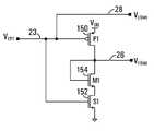
- FIG. 5is a schematic diagram of a biasing circuit provided by an embodiment of the invention.
- the biasing circuit of FIG. 5will be described in the context of its application in providing biasing voltages to the delay element of FIG. 2 . However, it is to be understood that the biasing circuit may find application to providing biasing voltages to other delay element designs.
- This circuitalso takes the input V ctrl 23 and produces biasing voltages V pbias 28 and V nbias 26 .
- the circuitdirectly connects the input voltage V ctrl 23 to V pbias 28 .
- V ctrl 23is also connected to the gate of transistor P 1 150 and the gate of transistor S 1 152 .
- Transistor P 1 150is connected to transistor S 1 152 through diode connected transistor M 1 154 .
- Transistor P 1 150is also connected to a supply voltage V DD .
- the bias voltage V nbias 26is taken at the drain of transistor M 1 154 .
- Transistor 51may be implemented with a size larger than that of M 1 to accommodate the current generated by M 1 .
- the purpose of this circuitis to mimic the DC behaviour of the biasing circuit of FIG. 3 .
- V ctrlwhen V ctrl is between 0.3V and 0.9V if can be seen that V ctrl and V pbias are approximately equal.
- this behaviouris reproduced by a direct connection between V ctrl 23 and V pbias 28 . Operation of the circuit for other values of V ctrl will result in different behaviour than that shown in FIG. 4 .
- the remaining circuitry of FIG. 5is for producing a V nbias that mimics the behaviour of V nbias shown in FIG. 4 for the circuit of FIG. 3 .
- V ctrl 23might for example be directly connected to the V pbias inputs of the differential delay elements, or the V pbias inputs might be generated in some other manner.
- V nbiasdrops sharply between 0.2 and 0.4 volts, and then levels off to a more moderate rate of decline between 0.4 volts and 1.0 volts.
- the curve 162 for V nbias in FIG. 6is very similar to the curve for V nbias 124 in FIG. 4 . Furthermore, the curve for V pbias in FIG. 6 is the same as curve 122 for V pbias in FIG. 4 over the range of 0.3 through 0.9 volts.
- V pbias , V nbias tog etherdefine the voltage swing at the output of the differential delay element.
- the effect of the inaccuracy in V pbias between 0.2 volts and 0.3 voltsis that the voltage will swing a little bit lower, and the swing will be non-symmetric.
- the assumptionis that the circuits operation is non-critical below 0.3 volts.
- Setting V pbiassets the swing.
- the biasing circuitincludes a complementary MOS output stage (P 1 150 , S 1 152 ) with a diode-connected transistor 154 in series between the two complementary transistors.
- the transistor 154clearly makes the operation very different from that of a standard CMOS output stage, which would have a steep transition between high and low states of the output voltage as the control or input voltage is changed.
- a feedback-free circuitthat produces the V nbias voltage from the control voltage such that the V nbias voltage is near a supply voltage V DD over a first control voltage range, sharply declines over a second control voltage range that follows the first control voltage range, and less sharply declines in a substantially linear manner over a third control voltage range that follows the second control voltage range.
- V DDis about 1V
- the first voltage rangeis from about 0V to about 0.2V
- the second voltage rangeis from about 0.2V to about 0.4V
- the third voltage rangeis a range above about 0.4V.
- the rangesare a function of V DD , for example 0 to 0.2 V DD , 0.2 V DD to 0.4 V DD and above 0.4 V DD .
- Another specific exampleis 0 to 0.3 V DD , 0.3 V DD to 0.5 V DD , and above 0.5 V DD .
- FIG. 7shown is a schematic diagram of another biasing network provided by an embodiment of the invention.
- This circuitagain receives the V ctrl 23 input and produces a V nbias output 26 .
- the input 23is connected to a pull-up network 200 and a pull-down network 204 .
- the circuit of FIG. 5is a specific example of the FIG. 7 embodiment.
- the pull-up network 200is P transistor 150
- the pull-down network 204is the transistor S 1 152
- the variable resistor 202is the diode connected transistor M 1 154 .
- other elementscan be used.
- the device elements and circuitsare connected to each other as shown in the figures, for the sake of simplicity.
- elements, circuits, etc.may be connected directly to each other.
- elements, circuits etc.may be connected indirectly to each other through other elements, circuits, etc., necessary for operation of the semiconductor ICs and DRAM devices.
- the circuit elements and devicesare coupled with (directly or indirectly connected to) each other.
Landscapes
- Physics & Mathematics (AREA)
- Nonlinear Science (AREA)
- Pulse Circuits (AREA)
- Amplifiers (AREA)
- Stabilization Of Oscillater, Synchronisation, Frequency Synthesizers (AREA)
Abstract
Description
Claims (10)
Priority Applications (1)
| Application Number | Priority Date | Filing Date | Title |
|---|---|---|---|
| US12/750,119US8035434B2 (en) | 2007-02-08 | 2010-03-30 | Simplified bias circuitry for differential buffer stage with symmetric loads |
Applications Claiming Priority (2)
| Application Number | Priority Date | Filing Date | Title |
|---|---|---|---|
| US11/703,634US7705642B2 (en) | 2007-02-08 | 2007-02-08 | Simplified bias circuitry for differential buffer stage with symmetric loads |
| US12/750,119US8035434B2 (en) | 2007-02-08 | 2010-03-30 | Simplified bias circuitry for differential buffer stage with symmetric loads |
Related Parent Applications (1)
| Application Number | Title | Priority Date | Filing Date |
|---|---|---|---|
| US11/703,634ContinuationUS7705642B2 (en) | 2007-02-08 | 2007-02-08 | Simplified bias circuitry for differential buffer stage with symmetric loads |
Publications (2)
| Publication Number | Publication Date |
|---|---|
| US20100182059A1 US20100182059A1 (en) | 2010-07-22 |
| US8035434B2true US8035434B2 (en) | 2011-10-11 |
Family
ID=39681209
Family Applications (2)
| Application Number | Title | Priority Date | Filing Date |
|---|---|---|---|
| US11/703,634Active2027-04-06US7705642B2 (en) | 2007-02-08 | 2007-02-08 | Simplified bias circuitry for differential buffer stage with symmetric loads |
| US12/750,119Expired - Fee RelatedUS8035434B2 (en) | 2007-02-08 | 2010-03-30 | Simplified bias circuitry for differential buffer stage with symmetric loads |
Family Applications Before (1)
| Application Number | Title | Priority Date | Filing Date |
|---|---|---|---|
| US11/703,634Active2027-04-06US7705642B2 (en) | 2007-02-08 | 2007-02-08 | Simplified bias circuitry for differential buffer stage with symmetric loads |
Country Status (3)
| Country | Link |
|---|---|
| US (2) | US7705642B2 (en) |
| TW (2) | TWI462111B (en) |
| WO (1) | WO2008095283A1 (en) |
Families Citing this family (2)
| Publication number | Priority date | Publication date | Assignee | Title |
|---|---|---|---|---|
| JP2011193334A (en)* | 2010-03-16 | 2011-09-29 | Elpida Memory Inc | Internal-clock adjusting circuit |
| US20130106504A1 (en)* | 2011-10-27 | 2013-05-02 | Taiwan Semiconductor Manufacturing Company, Ltd. | Integrated circuits with cascode transistor |
Citations (16)
| Publication number | Priority date | Publication date | Assignee | Title |
|---|---|---|---|---|
| US4857763A (en) | 1985-01-26 | 1989-08-15 | Kabushiki Kaisha Toshiba | MOS semiconductor integrated circuit in which the production of hot carriers near the drain of a short n channel conductivity type MOS transistor is decreased |
| US4959563A (en) | 1988-06-29 | 1990-09-25 | Texas Instruments Incorporated | Adjustable low noise output circuit |
| US5293082A (en) | 1988-06-21 | 1994-03-08 | Western Digital Corporation | Output driver for reducing transient noise in integrated circuits |
| US5378943A (en) | 1993-04-20 | 1995-01-03 | International Business Machines Corporation | Low power interface circuit |
| US5397935A (en) | 1992-03-27 | 1995-03-14 | Kabushiki Kaisha Toshiba | Bias current supplying circuit |
| US5561382A (en) | 1994-04-26 | 1996-10-01 | Mitsubishi Denki Kabushiki Kaisha | Bi-CMOS output buffer circuit for CMOS-to-ECL conversion |
| US5942940A (en) | 1997-07-21 | 1999-08-24 | International Business Machines Corporation | Low voltage CMOS differential amplifier |
| US5973524A (en) | 1998-03-25 | 1999-10-26 | Silsym, Inc. | Obtaining accurate on-chip time-constants and conductances |
| US5999017A (en) | 1997-07-03 | 1999-12-07 | Motorola, Inc. | CMOS implemented output buffer circuit for providing ECL level signals |
| US6249164B1 (en) | 1998-09-25 | 2001-06-19 | International Business Machines Corporation | Delay circuit arrangement for use in a DAC/driver waveform generator with phase lock rise time control |
| US6605997B1 (en) | 2002-02-08 | 2003-08-12 | International Business Machines Corporation | CMOS dual-stage differential receiver-amplifer |
| US6621314B2 (en) | 2001-09-25 | 2003-09-16 | Intel Corporation | Delay locked loop |
| US20060176096A1 (en)* | 2005-02-10 | 2006-08-10 | International Business Machines Corporation | Power supply insensitive delay element |
| US20070063687A1 (en) | 2005-09-20 | 2007-03-22 | Dacheng Zhou | Circuit and method for bias voltage generation |
| US7233201B2 (en) | 2004-08-31 | 2007-06-19 | Micron Technology, Inc. | Single-ended pseudo-differential output driver |
| US7279949B2 (en)* | 2005-02-11 | 2007-10-09 | International Business Machines Corporation | Programmable delay element |
Family Cites Families (1)
| Publication number | Priority date | Publication date | Assignee | Title |
|---|---|---|---|---|
| DE3709353A1 (en)* | 1987-03-21 | 1988-09-29 | Ruetgerswerke Ag | WATER-FREE APPLICATION FORM OF LOW MOLECULAR ALKALIHUMINATES |
- 2007
- 2007-02-08USUS11/703,634patent/US7705642B2/enactiveActive
- 2008
- 2008-01-30WOPCT/CA2008/000192patent/WO2008095283A1/enactiveApplication Filing
- 2008-02-01TWTW097103964Apatent/TWI462111B/ennot_activeIP Right Cessation
- 2008-02-01TWTW103130104Apatent/TW201511475A/enunknown
- 2010
- 2010-03-30USUS12/750,119patent/US8035434B2/ennot_activeExpired - Fee Related
Patent Citations (16)
| Publication number | Priority date | Publication date | Assignee | Title |
|---|---|---|---|---|
| US4857763A (en) | 1985-01-26 | 1989-08-15 | Kabushiki Kaisha Toshiba | MOS semiconductor integrated circuit in which the production of hot carriers near the drain of a short n channel conductivity type MOS transistor is decreased |
| US5293082A (en) | 1988-06-21 | 1994-03-08 | Western Digital Corporation | Output driver for reducing transient noise in integrated circuits |
| US4959563A (en) | 1988-06-29 | 1990-09-25 | Texas Instruments Incorporated | Adjustable low noise output circuit |
| US5397935A (en) | 1992-03-27 | 1995-03-14 | Kabushiki Kaisha Toshiba | Bias current supplying circuit |
| US5378943A (en) | 1993-04-20 | 1995-01-03 | International Business Machines Corporation | Low power interface circuit |
| US5561382A (en) | 1994-04-26 | 1996-10-01 | Mitsubishi Denki Kabushiki Kaisha | Bi-CMOS output buffer circuit for CMOS-to-ECL conversion |
| US5999017A (en) | 1997-07-03 | 1999-12-07 | Motorola, Inc. | CMOS implemented output buffer circuit for providing ECL level signals |
| US5942940A (en) | 1997-07-21 | 1999-08-24 | International Business Machines Corporation | Low voltage CMOS differential amplifier |
| US5973524A (en) | 1998-03-25 | 1999-10-26 | Silsym, Inc. | Obtaining accurate on-chip time-constants and conductances |
| US6249164B1 (en) | 1998-09-25 | 2001-06-19 | International Business Machines Corporation | Delay circuit arrangement for use in a DAC/driver waveform generator with phase lock rise time control |
| US6621314B2 (en) | 2001-09-25 | 2003-09-16 | Intel Corporation | Delay locked loop |
| US6605997B1 (en) | 2002-02-08 | 2003-08-12 | International Business Machines Corporation | CMOS dual-stage differential receiver-amplifer |
| US7233201B2 (en) | 2004-08-31 | 2007-06-19 | Micron Technology, Inc. | Single-ended pseudo-differential output driver |
| US20060176096A1 (en)* | 2005-02-10 | 2006-08-10 | International Business Machines Corporation | Power supply insensitive delay element |
| US7279949B2 (en)* | 2005-02-11 | 2007-10-09 | International Business Machines Corporation | Programmable delay element |
| US20070063687A1 (en) | 2005-09-20 | 2007-03-22 | Dacheng Zhou | Circuit and method for bias voltage generation |
Non-Patent Citations (4)
| Title |
|---|
| Golbus, Jason; Design of a 160 Mw, 1 Gigabit/Second, Serial I/O Link, Nov. 17, 1998, pp. 1-55. |
| Maneatis, John G.; et al.; Self-Biased High-Bandwidth Low-Jitter 1-TO-4096 Multiplier Clock Generator PLL; IEEE Journal of Solid-State Circuits, vol. 38, No. 11, Nov. 2003, pp. 1795-1803. |
| Maneatis, John G.; Low-Jitter and Process-Independent DLL and PLL Based on Self-Biased Techniques; ISSCC96/Session 8/Digital Clocks and Latches/Paper FA8.1; Feb. 9, 1996; pp. 130-132. |
| Seok-Woo Choi, Hong-June Park, "A PVT-insensitive CMOS putput driver with constant slew rate", Proceedings of 2004 IEEE Asia-Pacific Conference Advanced System Integrated Circuits (Aug. 4-5, 2004), pp. 116-119. ISBN: 0-7803-8637-X, INSPEC Accession No. 8083097. |
Also Published As
| Publication number | Publication date |
|---|---|
| US7705642B2 (en) | 2010-04-27 |
| US20100182059A1 (en) | 2010-07-22 |
| WO2008095283A1 (en) | 2008-08-14 |
| US20080191782A1 (en) | 2008-08-14 |
| TW200847177A (en) | 2008-12-01 |
| TW201511475A (en) | 2015-03-16 |
| TWI462111B (en) | 2014-11-21 |
Similar Documents
| Publication | Publication Date | Title |
|---|---|---|
| USRE49018E1 (en) | Charge pump for PLL/DLL | |
| US5994939A (en) | Variable delay cell with a self-biasing load | |
| US5767748A (en) | Voltage controlled oscillator and voltage controlled delay circuit | |
| US6628154B2 (en) | Digitally controlled analog delay locked loop (DLL) | |
| US7679418B2 (en) | Voltage level shifter and buffer using same | |
| US20040051576A1 (en) | Delay generator | |
| US7167052B2 (en) | Low voltage differential amplifier circuit for wide voltage range operation | |
| KR100400317B1 (en) | Delay circuit for clock synchronization device | |
| US8035434B2 (en) | Simplified bias circuitry for differential buffer stage with symmetric loads | |
| US7372341B2 (en) | Noise immunity circuitry for phase locked loops and delay locked loops | |
| US6507229B1 (en) | Voltage controlled delay circuit | |
| US9621022B1 (en) | Method and apparatus for generating complementary signals | |
| JP5689781B2 (en) | Gated VCO circuit | |
| KR20160082447A (en) | Voltage controlled delay circuit and voltage controlled oscillator including the same | |
| HK1095015A (en) | High output impedance charge pump for pll/dll | |
| HK1095015B (en) | High output impedance charge pump for pll/dll |
Legal Events
| Date | Code | Title | Description |
|---|---|---|---|
| AS | Assignment | Owner name:MOSAID TECHNOLOGIES INCORPORATED, CANADA Free format text:ASSIGNMENT OF ASSIGNORS INTEREST;ASSIGNOR:MAI, TONY;REEL/FRAME:024161/0992 Effective date:20070126 | |
| FEPP | Fee payment procedure | Free format text:PAYOR NUMBER ASSIGNED (ORIGINAL EVENT CODE: ASPN); ENTITY STATUS OF PATENT OWNER: LARGE ENTITY | |
| AS | Assignment | Owner name:ROYAL BANK OF CANADA, CANADA Free format text:U.S. INTELLECTUAL PROPERTY SECURITY AGREEMENT (FOR NON-U.S. GRANTORS) - SHORT FORM;ASSIGNORS:658276 N.B. LTD.;658868 N.B. INC.;MOSAID TECHNOLOGIES INCORPORATED;REEL/FRAME:027512/0196 Effective date:20111223 | |
| AS | Assignment | Owner name:CONVERSANT INTELLECTUAL PROPERTY MANAGEMENT INC., Free format text:CHANGE OF NAME;ASSIGNOR:MOSAID TECHNOLOGIES INCORPORATED;REEL/FRAME:032439/0638 Effective date:20140101 | |
| RF | Reissue application filed | Effective date:20131010 | |
| AS | Assignment | Owner name:CONVERSANT IP N.B. 868 INC., CANADA Free format text:RELEASE OF SECURITY INTEREST;ASSIGNOR:ROYAL BANK OF CANADA;REEL/FRAME:033484/0344 Effective date:20140611 Owner name:CONVERSANT INTELLECTUAL PROPERTY MANAGEMENT INC., Free format text:RELEASE OF SECURITY INTEREST;ASSIGNOR:ROYAL BANK OF CANADA;REEL/FRAME:033484/0344 Effective date:20140611 Owner name:CONVERSANT IP N.B. 276 INC., CANADA Free format text:RELEASE OF SECURITY INTEREST;ASSIGNOR:ROYAL BANK OF CANADA;REEL/FRAME:033484/0344 Effective date:20140611 | |
| AS | Assignment | Owner name:CONVERSANT INTELLECTUAL PROPERTY MANAGEMENT INC., CANADA Free format text:CHANGE OF ADDRESS;ASSIGNOR:CONVERSANT INTELLECTUAL PROPERTY MANAGEMENT INC.;REEL/FRAME:033678/0096 Effective date:20140820 Owner name:CONVERSANT INTELLECTUAL PROPERTY MANAGEMENT INC., Free format text:CHANGE OF ADDRESS;ASSIGNOR:CONVERSANT INTELLECTUAL PROPERTY MANAGEMENT INC.;REEL/FRAME:033678/0096 Effective date:20140820 | |
| AS | Assignment | Owner name:ROYAL BANK OF CANADA, AS LENDER, CANADA Free format text:U.S. PATENT SECURITY AGREEMENT (FOR NON-U.S. GRANTORS);ASSIGNOR:CONVERSANT INTELLECTUAL PROPERTY MANAGEMENT INC.;REEL/FRAME:033706/0367 Effective date:20140611 Owner name:CPPIB CREDIT INVESTMENTS INC., AS LENDER, CANADA Free format text:U.S. PATENT SECURITY AGREEMENT (FOR NON-U.S. GRANTORS);ASSIGNOR:CONVERSANT INTELLECTUAL PROPERTY MANAGEMENT INC.;REEL/FRAME:033706/0367 Effective date:20140611 | |
| REMI | Maintenance fee reminder mailed | ||
| LAPS | Lapse for failure to pay maintenance fees | ||
| STCH | Information on status: patent discontinuation | Free format text:PATENT EXPIRED DUE TO NONPAYMENT OF MAINTENANCE FEES UNDER 37 CFR 1.362 | |
| FP | Lapsed due to failure to pay maintenance fee | Effective date:20151011 | |
| AS | Assignment | Owner name:CONVERSANT INTELLECTUAL PROPERTY MANAGEMENT INC., CANADA Free format text:RELEASE OF U.S. PATENT AGREEMENT (FOR NON-U.S. GRANTORS);ASSIGNOR:ROYAL BANK OF CANADA, AS LENDER;REEL/FRAME:047645/0424 Effective date:20180731 Owner name:CONVERSANT INTELLECTUAL PROPERTY MANAGEMENT INC., Free format text:RELEASE OF U.S. PATENT AGREEMENT (FOR NON-U.S. GRANTORS);ASSIGNOR:ROYAL BANK OF CANADA, AS LENDER;REEL/FRAME:047645/0424 Effective date:20180731 |