US8034702B2 - Methods of forming through substrate interconnects - Google Patents
Methods of forming through substrate interconnectsDownload PDFInfo
- Publication number
- US8034702B2 US8034702B2US11/840,120US84012007AUS8034702B2US 8034702 B2US8034702 B2US 8034702B2US 84012007 AUS84012007 AUS 84012007AUS 8034702 B2US8034702 B2US 8034702B2
- Authority
- US
- United States
- Prior art keywords
- dielectric
- substrate
- passivation
- dielectric material
- over
- Prior art date
- Legal status (The legal status is an assumption and is not a legal conclusion. Google has not performed a legal analysis and makes no representation as to the accuracy of the status listed.)
- Active, expires
Links
Images


Classifications
- H—ELECTRICITY
- H01—ELECTRIC ELEMENTS
- H01L—SEMICONDUCTOR DEVICES NOT COVERED BY CLASS H10
- H01L21/00—Processes or apparatus adapted for the manufacture or treatment of semiconductor or solid state devices or of parts thereof
- H01L21/70—Manufacture or treatment of devices consisting of a plurality of solid state components formed in or on a common substrate or of parts thereof; Manufacture of integrated circuit devices or of parts thereof
- H01L21/71—Manufacture of specific parts of devices defined in group H01L21/70
- H01L21/768—Applying interconnections to be used for carrying current between separate components within a device comprising conductors and dielectrics
- H01L21/76898—Applying interconnections to be used for carrying current between separate components within a device comprising conductors and dielectrics formed through a semiconductor substrate
- H—ELECTRICITY
- H01—ELECTRIC ELEMENTS
- H01L—SEMICONDUCTOR DEVICES NOT COVERED BY CLASS H10
- H01L21/00—Processes or apparatus adapted for the manufacture or treatment of semiconductor or solid state devices or of parts thereof
- H01L21/02—Manufacture or treatment of semiconductor devices or of parts thereof
- H01L21/02104—Forming layers
- H01L21/02107—Forming insulating materials on a substrate
- H01L21/02225—Forming insulating materials on a substrate characterised by the process for the formation of the insulating layer
- H01L21/0226—Forming insulating materials on a substrate characterised by the process for the formation of the insulating layer formation by a deposition process
- H01L21/02282—Forming insulating materials on a substrate characterised by the process for the formation of the insulating layer formation by a deposition process liquid deposition, e.g. spin-coating, sol-gel techniques, spray coating
- H—ELECTRICITY
- H01—ELECTRIC ELEMENTS
- H01L—SEMICONDUCTOR DEVICES NOT COVERED BY CLASS H10
- H01L21/00—Processes or apparatus adapted for the manufacture or treatment of semiconductor or solid state devices or of parts thereof
- H01L21/70—Manufacture or treatment of devices consisting of a plurality of solid state components formed in or on a common substrate or of parts thereof; Manufacture of integrated circuit devices or of parts thereof
- H01L21/71—Manufacture of specific parts of devices defined in group H01L21/70
- H01L21/768—Applying interconnections to be used for carrying current between separate components within a device comprising conductors and dielectrics
- H01L21/76801—Applying interconnections to be used for carrying current between separate components within a device comprising conductors and dielectrics characterised by the formation and the after-treatment of the dielectrics, e.g. smoothing
- H01L21/76829—Applying interconnections to be used for carrying current between separate components within a device comprising conductors and dielectrics characterised by the formation and the after-treatment of the dielectrics, e.g. smoothing characterised by the formation of thin functional dielectric layers, e.g. dielectric etch-stop, barrier, capping or liner layers
- H01L21/76831—Applying interconnections to be used for carrying current between separate components within a device comprising conductors and dielectrics characterised by the formation and the after-treatment of the dielectrics, e.g. smoothing characterised by the formation of thin functional dielectric layers, e.g. dielectric etch-stop, barrier, capping or liner layers in via holes or trenches, e.g. non-conductive sidewall liners
Definitions
- Embodiments disclosed hereinpertain to methods of forming through substrate interconnects.
- Integrated circuitsare commonly fabricated using semiconductor substrates. Numerous processes are used in the fabrication of the circuits, including, for example, deposition of material, etching of material, doping, photolithography, metallization, oxidation, etc. Most often, a plurality of identical integrated circuits are formed over a single substrate, commonly referred to as a wafer, to define individual circuit die. These are ultimately singulated into separated die or chips, which are then packaged. In other applications, a single wafer or other substrate might be fabricated to comprise one or more different integrated circuits, and may not be singulated. Regardless, a continuing goal in the fabrication of integrated circuitry is to make ever denser and smaller devices, and resultant integrated circuitry.
- One manner of increasing density in a semiconductor assemblyis to stack individual substrates, such as semiconductor die, one upon another.
- the stacked semiconductor diemay be interconnected by forming conductive vias in through holes in one or more of the semiconductor dies, for example prior to singulation.
- An interior of each of the viasmay be coated with an electrically insulating material followed by an electrically conductive material to electrically connect the vias to integrated circuitry fabricated on a primary circuitry side of the substrate.
- the conductive viasprovide a conductive pathway from the primary circuitry side of a semiconductor substrate to its back-side or back-surface for conductive contact with another substrate.
- the integrated circuit diewhen near completion and prior to singulation, are usually provided with one or more dielectric passivation layers on one or both sides of the substrate. Such layers might provide one or more of insulative protection, stress buffering, and/or a moisture barrier to underlying circuitry.
- the through hole viasare then formed through the passivation layer(s) and into semiconductive and other material of the substrate. As above, in order to isolate the conductive portion of the through substrate interconnect from other portions of the substrate, the vias are lined with one or more electrically insulating materials. As the throughway for vias become narrower, it can be problematic to completely line sidewalls of such vias with dielectric material prior to forming conductive material therein.
- One existing manner of doing socomprises pulsed chemical vapor deposition of an aluminum oxide-comprising material. Such is deposited over the dielectric layer and into the via to line the sidewalls of the via. Differences in thermal coefficients of expansion among the aluminum oxide-comprising material, the passivation dielectric material and materials of the substrate can undesirably cause separation and cracking or one or more of these materials.
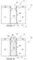
- FIG. 1is a diagrammatic sectional view of a semiconductor substrate in process in accordance with an embodiment of the invention.
- FIGS. 2-5illustrate a method embodiment of the invention.
- FIG. 6is a diagrammatic sectional view of another semiconductor substrate in process in accordance with an embodiment of the invention.
- FIGS. 7 and 8illustrate a method embodiment of the invention.
- FIG. 9is a diagrammatic sectional view of another semiconductor substrate in process in accordance with an embodiment of the invention.
- FIGS. 10-12illustrate a method embodiment of the invention.
- FIG. 13is a diagrammatic sectional view of another semiconductor substrate in process in accordance with an embodiment of the invention.
- FIGS. 14-17illustrate a method embodiment of the invention.
- FIG. 18is a diagrammatic sectional view of another semiconductor substrate in process in accordance with an embodiment of the invention.
- FIG. 19is a diagrammatic sectional view of another semiconductor substrate in process in accordance with an embodiment of the invention.
- FIGS. 20 and 21illustrate a method embodiment of the invention.
- Embodiments of the inventionencompass methods of forming through substrate interconnects, sometimes referred to in the existing art as through wafer interconnects.
- a “through substrate interconnect”is a conductive interconnect extending from a back-side of a semiconductor substrate to integrated circuitry formed on or proximate a front-side of the substrate.
- the “front-side” of a semiconductor substrateis that one of the two major opposing sides of the substrate (the other being the “back-side”) from which the circuit components of the integrated circuitry are primarily fabricated.
- semiconductor substrateor “semiconductive substrate” is defined to mean any construction comprising semiconductive material, including, but not limited to, bulk semiconductive materials such as a semiconductive wafer (either alone or in assemblies comprising other materials thereon), and semiconductive material layers (either alone or in assemblies comprising other materials).
- substraterefers to any supporting structure, including, but not limited to, the semiconductive substrates described above.
- a semiconductor substrateis indicated generally with reference numeral 10 , and comprises a first major side 12 and a second major side 14 .
- a thickness range for substrate 10is from about 700 microns to about 800 microns.
- Side 12may comprise a back-side of the semiconductor substrate and side 14 may comprise a front-side of the semiconductor substrate.
- side 12may comprise the front-side of the semiconductor substrate and side 14 may comprise the back-side of the semiconductor substrate.
- semiconductor substrate 10is depicted as comprising some region 16 and a passivation dielectric layer 18 has been formed thereover.
- a “passivation dielectric”is any dielectric material formed over an outer surface of a substrate after completion of most all of the integrated circuit components. Redistribution layers and/or other conductive lines might be formed over passivation dielectric 18 , and other insulating and/or passivating layers might be provided thereover as well, but regardless the vast majority of the integrated circuit devices has been fabricated inwardly of the passivation dielectric in what is generally depicted as region 16 . Accordingly, region 16 will include a plurality of different materials, layers, and regions having integrated circuit components and devices (not shown) fabricated therein, including at least some semiconductive material.
- FIG. 1depicts passivation dielectric 18 being deposited onto substrate side 12 .
- substrate region 16comprises bulk semiconductor material
- substrate side 12comprises the back-side
- passivation dielectric 18has been formed over bulk semiconductive material of substrate region 16 .
- Siliconfor example bulk monocrystalline silicon, is but one example semiconductive material.
- An example thickness range for layer 18is from 1 micron to 25 microns.
- example materials for layer 18include polyimide, polybenzoxazole, spin-on dielectric, and epoxies.
- a via 20has been formed through passivation dielectric 18 and into semiconductive material of substrate 10 from side 12 . Such may comprise a through via at this point or subsequent in the processing.
- a “through via”is at some point a passageway extending from a substrate back-side to at least proximate a substrate front-side for ultimate conductive connection with one or more circuit devices on the front-side or with another substrate received over/proximate the front-side.
- via 20can be considered as comprising sidewalls 22 and a base 24 .
- FIG. 2also depicts via 20 as only being formed partially through substrate 10 , although formation of via 20 completely through substrate 10 might also be utilized.
- substrate 10might be thinned by polishing or other action prior to or after forming via 20 , and regardless of whether via 20 extends partially or completely through substrate 10 .
- cross-sectional configurations for via 20are circular or oval, having an example minimum diameter/cross-dimension of from about 5 microns to about 70 microns.
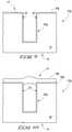
- a liquid dielectric 30has been applied over passivation dielectric 18 and into via 20 to line at least an elevationally outermost portion of via sidewalls 22 relative substrate side 12 from which via 20 was at least initially formed.
- the application of a liquid dielectric 30lines all of sidewalls 22 of via 20 with liquid dielectric 30 , and completely covers base 24 of via 20 with liquid dielectric 30 .
- liquid dielectric 30may line only an elevationally outermost portion of sidewalls 22 relative substrate side 12 , for example only 5%, 25%, 50%, 75%, etc. of the outermost elevational length of sidewalls 22 of via 20 .
- liquid dielectric 30might be applied to line all of sidewalls 22 yet only a portion of via base 24 , or only a portion of sidewalls 22 and none of via base 24 .
- the application of liquid dielectriclines all sidewalls of at least passivation dielectric 18 of via 20 with dielectric material 30 .
- the application of liquid dielectric linesat least an elevationally outermost portion of semiconductive material sidewalls of via 20 inward of passivation dielectric 18 with liquid dielectric 30 , for example where substrate side 12 is the back-side and semiconductor region 16 immediately adjacent passivation dielectric 18 comprises bulk semiconductor material, for example silicon.
- the liquid dielectric 30comprises a liquid polymer, and regardless in one embodiment comprises a spin-on dielectric applied over substrate side 12 in a spin-on manner, and whether by an existing method or a yet-to-be developed method.
- any suitable flowable dielectricis contemplated whether existing or yet-to-be developed, and whether provided onto substrate 10 by spin-on or other technique.
- Example materialsare JSR WPR-S170P available from JSR Corporation of Tokyo, Japan, CRC-7561 available from Sumitomo Bakelite of Tokyo, Japan, and SINR-3150HSM from Shin-Etsu MicroSi of Phoenix, Ariz.
- spin coating times and rpmsmight be utilized where spin coating is used to achieve desired degree of covering of liquid dielectric 30 relative to one or both via sidewalls 22 and via base 24 .
- Spin-on dielectric applicationmay be desirable to take advantage of simpler and lower cost existing such techniques without requiring vacuum processing.
- Liquid dielectric 30 within via 20is solidified, and conductive material is formed within via 20 over solidified dielectric 30 and a through substrate interconnect is formed with the conductive material.
- the solidifyingis effective to adhere and cease flow of material 30 relative to substrate 16 / 18 , and may include one or more elevated temperature baking steps to drive solvent from material 30 as part of ultimate solidification.
- application of liquid dielectric 30 to a desired thickness and coverage relative to all or portions of sidewalls 22 and/or base 24might occur or be conducted in a single liquid dielectric application step, or in multiple separate liquid dielectric application steps which may or may not include one or more elevated baking steps in between separate spaced liquid applications.
- FIGS. 4 and 5depict subsequent processing of the FIG. 3 substrate.
- substrate 10has been subjected to example substrate-side 14 polishing to effectively thin substrate 10 at least to a point of exposing via 20 .
- via 20extends completely through substrate 10 from substrate side 12 to substrate side 14 .
- solidified dielectric 30might be subjected to an anisotropic etch to remove material 30 from being received over passivation dielectric 18 and from over via base 24 (not shown).
- conductive material 32has been formed within via 20 , and a through substrate interconnect 35 has been formed therewith.
- Example materials 32include any conductive material, including conductively doped semiconductive materials, elemental metals, alloys of elemental metals, and/or conductive metal compounds, including any combinations thereof.
- a method of forming a through substrate interconnectis conducted to be void of using any chemical vapor deposition of any dielectric material to within via 20 .
- FIGS. 4 and 5depict one embodiment wherein example polishing of substrate side 14 occurred prior to forming of conductive material within via 20 . Such could of course be reversed wherein some or all of conductive material 32 is deposited within via 20 of the FIG. 3 substrate prior to the example polishing of FIG. 4 .
- semiconductor substrate 10 acan be considered as having substrate side 12 being the back-side, and substrate side 14 as being the substrate front-side. In one embodiment, semiconductor substrate 10 a can be considered as having substrate side 12 being the front-side, and substrate side 14 as being the substrate back-side.
- FIG. 6depicts substrate side 14 as comprising a conductive bond pad 36 , which is thereby depicted as being more proximate substrate side 14 than substrate side 12 .
- Bond pad 36can be considered as comprising a back-side 38 .
- Via 20 ahas been formed to conductive bond pad 36 from side 12 . Such might be formed partially into bond pad 36 or to extend completely therethrough (not shown).
- FIG. 6depicts via 20 a extending to essentially stop on via back-side 38 .
- a liquid dielectric 30 ahas been applied to line at least an elevationally outermost portion of sidewalls 22 of via 20 a .
- the FIG. 6 embodimentalso depicts application of liquid dielectric 30 a over back-side 38 of bond
- liquid dielectric 30 ahas been solidified and subjected to any suitable anisotropic etch which removes material 30 a from being received elevationally outward of passivation dielectric 18 and from over back-side 38 of bond pad 36 .
- conductive material 32 ahas been formed within via 20 a and a through substrate interconnect 35 a has been formed therewith.
- Material compositionmay be as described in the above embodiments.
- FIGS. 9-12Additional embodiments are next described with reference to FIGS. 9-12 in connection with a semiconductor substrate 10 b .
- Like numerals from the first-described embodimentsare utilized where appropriate, with differences being indicated with the suffix “b” or with different numerals.
- Not all embodiments of the inventionrequire deposit of a passivation dielectric layer over a semiconductor substrate.
- the above-depicted embodimentsprovide but examples where a passivation dielectric layer is deposited over the side of the substrate from which the via is formed before forming the via, and then forming the via through the passivation dielectric layer.
- FIGS. 9-12depict an embodiment wherein a passivation dielectric layer is deposited over the side of the substrate from which the via is at least initially formed after initially forming the via.
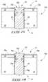
- a via 20 bhas been formed into semiconductive material of semiconductor substrate 10 b from substrate side 12 .
- Liquid dielectric 30 bhas been applied to line at least an elevationally outermost portion of sidewalls 22 of via 20 b , for example using any of the materials, manners and resultant constructions as described with the above embodiments.
- liquid dielectric 30 bhas been solidified within via 20 b , and a passivation dielectric 18 b has been formed over substrate side 12 and at least partially over via 20 b .
- passivation dielectric 18 bis formed over all of via 20 b .
- passivation dielectric 18 bextends to within via 20 b at least to some degree. In another embodiment, none of the passivation dielectric layer extends to within the via, for example bridging partially or wholly thereover without any lower portion thereof extending therein (not shown).
- the passivation dielectric layeris removed from over the via (and in one embodiment from being over and within the via), and conductive material is formed within the via over the solidified dielectric and a through substrate interconnect is formed therewith.
- FIGS. 11 and 12depict one such example manner of doing so.
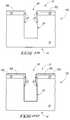
- FIG. 11depicts formation of a mask 42 over passivation dielectric 18 b .
- an example masking materialis photoresist that is patterned using photolithographic techniques.
- layers 42 and 18 bmight be of the same composition, for example photosensitive polyimide.
- mask 42is depicted as comprising an opening 43 therethrough to via 20 b , and passivation dielectric 18 b has been etched through opening 43 to be removed from over and from within via 20 b.
- FIG. 12depicts thinning of substrate 10 b from substrate side 14 to expose via 20 b prior to formation of conductive material 32 b within via 20 b . Any alternate methods are contemplated, including by way of example that described above generally in connection with FIGS. 1-8 .
- FIGS. 13-17Additional embodiments are next described in connection with FIGS. 13-17 with respect to a semiconductor substrate 10 d .
- Like numerals from the above-described embodimentsare utilized where appropriate, with differences being indicated with the suffix “d” or with different numerals.
- the above-described examplesdo not require, and may be void of, any vapor deposition of dielectric material to line any portion of the depicted via after its formation.
- certain embodiments of the inventiondo contemplate some combination of vapor depositing of a dielectric material within a via in the fabrication of a through substrate interconnect in combination with some application of a liquid dielectric within a via in the fabrication of a through substrate interconnect.
- existing and yet-to-be developed vapor deposition methodsmight be better capable of lining through vias having very high aspect ratios as compared to existing and yet-to-be developed liquid dielectric application techniques.
- another reason for doing somight be to provide vapor deposited dielectric at the base of a via while providing a liquid dielectric proximate the via opening top which has a solidified coefficient of thermal expansion which is between that of the passivation dielectric layer and the vapor deposited dielectric.
- a passivation dielectric 18has been formed over substrate side 12 of semiconductor substrate 10 d .
- a via 20has been formed through passivation dielectric 18 and into semiconductive material of substrate 10 d from substrate side 12 .
- a dielectric material 50has been vapor deposited over passivation dielectric 18 to line at least an elevationally outermost portion of sidewalls 22 of via 20 .
- Any suitable dielectric material 50might be used.
- the vapor depositingcomprises chemical vapor depositing, and in one embodiment comprises pulsed chemical vapor depositing.
- One example dielectric material 50comprises aluminum oxide, although other materials in combination with or exclusive of aluminum oxide are also of course contemplated.
- Dielectric material 50might be deposited to completely line all of via sidewalls 22 as shown, or only at least an elevationally outermost portion thereof.
- An example thickness for vapor deposit dielectric material 50is from about 0.1 micron to about 1 micron.
- Dielectric material 50might be recessed (for example by etching) to within the via, for example to be at or below the passivation dielectric.
- dielectric material 50has been recessed to below the base of passivation dielectric 18 within via 20 .
- such recessingis conducted without any masking over substrate 10 .
- the recessing of dielectric material 50 within via 20is such that it is received at least 2 microns elevationally inward of the base of passivation dielectric 18 .
- the dielectric material 50might be recessed to have its top coincide with the base of passivation dielectric 18 (not shown) or received elevationally outward thereof (not shown). Regardless in the depicted embodiment, such recessing of dielectric material 50 is shown as also effectively clearing it from being received atop passivation dielectric 18 and from over base 24 of via 20 between sidewall-received portions of dielectric material 50 .
- liquid dielectric 30 dhas been applied over passivation dielectric 18 into via 20 at least to line an elevationally outermost portion of sidewalls 22 of via 20 above recessed dielectric material 50 and to be received over at least an elevationally outermost portion of recessed dielectric material 50 received within via 20 .
- Example liquid dielectric materials and methods of applicationare as described above. Liquid dielectric 30 d might be applied to completely cover over sidewalls of vapor deposited dielectric material 50 (not shown), or only partially received over an elevationally outermost portion thereof (as shown). Further, liquid dielectric material 30 d may or may not cover any portion of via base 24 .
- the liquid dielectricis solidified within the via, and conductive material is formed therewithin over the solidified dielectric and a through substrate interconnect is formed with the conductive material.
- conductive material 32 dis formed therewithin over the solidified dielectric and a through substrate interconnect is formed with the conductive material.
- FIG. 17One example resultant construction is depicted in FIG. 17 in conjunction with conductive material 32 d in the fabrication of a through substrate interconnect 35 d .
- any of the above-described attributes, methods, constructions, and materialsmight be used or alternately be formed.
- passivation dielectric 18 and dielectric material 50are formed to have different coefficients of thermal expansion, with liquid dielectric 30 d being solidified to have a coefficient of thermal expansion which is between those of passivation dielectric 18 and vapor deposited dielectric material 50 .
- liquid dielectric 30 dis solidified to have a low Young's Modulus of less than or equal to approximately 2.0 GPa.
- FIG. 18depicts vapor deposited dielectric material 50 e as not having been recessed within via 20 prior to application and solidification of liquid dielectric 30 e . Materials and manners of processing and construction can otherwise be as described in connection with all of the above embodiments.
- FIGS. 19-21Additional embodiment methods of forming through substrate interconnects are next described with reference to FIGS. 19-21 with respect to a semiconductor substrate 10 f .
- Like numerals from the first-described embodimentare utilized where appropriate, with differences being indicated with the suffix “f” or with different numerals.
- FIGS. 13-18 embodimentsapplied a liquid dielectric after forming a vapor deposited dielectric within a through via.
- FIGS. 19-21depict an alternate embodiment wherein a vapor deposited dielectric material is formed after application and solidification of a liquid dielectric material.
- FIG. 19depicts formation of a passivation dielectric 18 over substrate side 12 , and a via 20 therethrough and into semiconductive material of substrate 10 f from substrate side 12 .
- a liquid dielectric 30 fhas been applied over passivation dielectric 18 and into via 20 to line only an elevationally outermost portion of sidewalls 22 of via 20 .
- such linesno more than 50% of a combined elevational height/thickness of via 20 within passivation dielectric 18 and the depicted substrate region 16 .
- liquid dielectric 30 fis solidified and a dielectric material 50 f is vapor deposited to within via 20 over solidified dielectric 30 f and to line over sidewall portions 22 of via 20 that are received elevationally inward of solidified dielectric 30 f within via 20 .
- dielectric material 50 fis completely covering of all sidewalls 22 of via 20 , and also covering of all of base 24 of via 20 , although such is not required.
- Conductive materialis ultimately formed within via 20 over the vapor deposited dielectric material and solidified dielectric to form a through substrate interconnect, for example as shown in FIG. 21 of material 32 f to form a through substrate interconnect 35 f .
- solidified spin-on dielectric 30 fmay be provided to have a coefficient of thermal expansion which is between that of passivation dielectric layer 18 and dielectric material 50 f.
Landscapes
- Engineering & Computer Science (AREA)
- Physics & Mathematics (AREA)
- Condensed Matter Physics & Semiconductors (AREA)
- General Physics & Mathematics (AREA)
- Manufacturing & Machinery (AREA)
- Computer Hardware Design (AREA)
- Microelectronics & Electronic Packaging (AREA)
- Power Engineering (AREA)
- Internal Circuitry In Semiconductor Integrated Circuit Devices (AREA)
Abstract
Description
Claims (23)
Priority Applications (11)
| Application Number | Priority Date | Filing Date | Title |
|---|---|---|---|
| US11/840,120US8034702B2 (en) | 2007-08-16 | 2007-08-16 | Methods of forming through substrate interconnects |
| CN2008801028774ACN101809725B (en) | 2007-08-16 | 2008-07-16 | Method of forming through-substrate interconnect |
| PCT/US2008/070141WO2009025942A1 (en) | 2007-08-16 | 2008-07-16 | Methods of forming through substrate interconnects |
| CN201110415712.6ACN102522369B (en) | 2007-08-16 | 2008-07-16 | Methods of forming through substrate interconnects |
| KR1020107003282AKR101125994B1 (en) | 2007-08-16 | 2008-07-16 | Methods of forming through substrate interconnects |
| SG2012059887ASG183724A1 (en) | 2007-08-16 | 2008-07-16 | Methods of forming through substrate interconnects |
| TW097131015ATWI370517B (en) | 2007-08-16 | 2008-08-14 | Methods of forming through substrate interconnects |
| US13/248,970US8629060B2 (en) | 2007-08-16 | 2011-09-29 | Methods of forming through substrate interconnects |
| US14/100,893US8927410B2 (en) | 2007-08-16 | 2013-12-09 | Methods of forming through substrate interconnects |
| US14/561,642US9685375B2 (en) | 2007-08-16 | 2014-12-05 | Methods of forming through substrate interconnects |
| US15/602,627US10685882B2 (en) | 2007-08-16 | 2017-05-23 | Methods of forming through substrate interconnects |
Applications Claiming Priority (1)
| Application Number | Priority Date | Filing Date | Title |
|---|---|---|---|
| US11/840,120US8034702B2 (en) | 2007-08-16 | 2007-08-16 | Methods of forming through substrate interconnects |
Related Child Applications (1)
| Application Number | Title | Priority Date | Filing Date |
|---|---|---|---|
| US13/248,970DivisionUS8629060B2 (en) | 2007-08-16 | 2011-09-29 | Methods of forming through substrate interconnects |
Publications (2)
| Publication Number | Publication Date |
|---|---|
| US20090047781A1 US20090047781A1 (en) | 2009-02-19 |
| US8034702B2true US8034702B2 (en) | 2011-10-11 |
Family
ID=40363301
Family Applications (5)
| Application Number | Title | Priority Date | Filing Date |
|---|---|---|---|
| US11/840,120Active2028-06-25US8034702B2 (en) | 2007-08-16 | 2007-08-16 | Methods of forming through substrate interconnects |
| US13/248,970Active2028-02-13US8629060B2 (en) | 2007-08-16 | 2011-09-29 | Methods of forming through substrate interconnects |
| US14/100,893ActiveUS8927410B2 (en) | 2007-08-16 | 2013-12-09 | Methods of forming through substrate interconnects |
| US14/561,642Active2027-09-02US9685375B2 (en) | 2007-08-16 | 2014-12-05 | Methods of forming through substrate interconnects |
| US15/602,627Active2027-09-03US10685882B2 (en) | 2007-08-16 | 2017-05-23 | Methods of forming through substrate interconnects |
Family Applications After (4)
| Application Number | Title | Priority Date | Filing Date |
|---|---|---|---|
| US13/248,970Active2028-02-13US8629060B2 (en) | 2007-08-16 | 2011-09-29 | Methods of forming through substrate interconnects |
| US14/100,893ActiveUS8927410B2 (en) | 2007-08-16 | 2013-12-09 | Methods of forming through substrate interconnects |
| US14/561,642Active2027-09-02US9685375B2 (en) | 2007-08-16 | 2014-12-05 | Methods of forming through substrate interconnects |
| US15/602,627Active2027-09-03US10685882B2 (en) | 2007-08-16 | 2017-05-23 | Methods of forming through substrate interconnects |
Country Status (6)
| Country | Link |
|---|---|
| US (5) | US8034702B2 (en) |
| KR (1) | KR101125994B1 (en) |
| CN (2) | CN101809725B (en) |
| SG (1) | SG183724A1 (en) |
| TW (1) | TWI370517B (en) |
| WO (1) | WO2009025942A1 (en) |
Families Citing this family (11)
| Publication number | Priority date | Publication date | Assignee | Title |
|---|---|---|---|---|
| US8034702B2 (en) | 2007-08-16 | 2011-10-11 | Micron Technology, Inc. | Methods of forming through substrate interconnects |
| JP5237607B2 (en)* | 2007-10-25 | 2013-07-17 | 新光電気工業株式会社 | Substrate manufacturing method |
| JP5455538B2 (en)* | 2008-10-21 | 2014-03-26 | キヤノン株式会社 | Semiconductor device and manufacturing method thereof |
| JP5596919B2 (en)* | 2008-11-26 | 2014-09-24 | キヤノン株式会社 | Manufacturing method of semiconductor device |
| CN102299098B (en)* | 2010-06-23 | 2014-08-13 | 上海华虹宏力半导体制造有限公司 | Method for forming contact hole structure |
| US8779559B2 (en) | 2012-02-27 | 2014-07-15 | Qualcomm Incorporated | Structure and method for strain-relieved TSV |
| CN104465498B (en)* | 2014-11-12 | 2017-12-22 | 华天科技(昆山)电子有限公司 | The method that silicon hole inwall uniformly applies insulating layer coating |
| NL2014598B1 (en)* | 2015-04-08 | 2017-01-20 | Suss Microtec Lithography Gmbh | Method for coating a substrate. |
| US9786619B2 (en)* | 2015-12-31 | 2017-10-10 | Taiwan Semiconductor Manufacturing Company, Ltd. | Semiconductor structure and manufacturing method thereof |
| CN110610922B (en)* | 2018-06-14 | 2021-10-26 | 华邦电子股份有限公司 | Contact structure and forming method thereof |
| US20200043785A1 (en)* | 2018-07-31 | 2020-02-06 | Winbond Electronics Corp. | A contact structure having a first liner and a second liner formed between a conductive element and a insulating layer |
Citations (21)
| Publication number | Priority date | Publication date | Assignee | Title |
|---|---|---|---|---|
| US4603023A (en)* | 1983-12-01 | 1986-07-29 | International Business Machines Corporation | Method of making a hybrid dielectric probe interposer |
| US5425816A (en)* | 1991-08-19 | 1995-06-20 | Spectrolab, Inc. | Electrical feedthrough structure and fabrication method |
| US5858869A (en) | 1997-06-03 | 1999-01-12 | Industrial Technology Research Institute | Method for fabricating intermetal dielectric insulation using anisotropic plasma oxides and low dielectric constant polymers |
| US5955200A (en) | 1997-11-18 | 1999-09-21 | United Microelectronics Corp. | Structure for reducing stress between metallic layer and spin-on-glass layer |
| KR19990082267A (en) | 1996-12-04 | 1999-11-25 | 야스카와 히데아키 | Electronic components and semiconductor devices, manufacturing methods and mounting methods thereof, circuit boards and electronic devices |
| US6121130A (en) | 1998-11-16 | 2000-09-19 | Chartered Semiconductor Manufacturing Ltd. | Laser curing of spin-on dielectric thin films |
| JP2000323605A (en) | 1999-05-10 | 2000-11-24 | Hitachi Ltd | Semiconductor device, method of manufacturing the same, and electronic equipment using the same |
| US6255737B1 (en) | 1996-12-04 | 2001-07-03 | Seiko Epson Corporation | Semiconductor device and method of making the same, circuit board, and electronic instrument |
| US6475896B1 (en) | 1996-12-04 | 2002-11-05 | Seiko Epson Corporation | Electronic component and semiconductor device, method of making the same and method of mounting the same, circuit board, and electronic instrument |
| US20020182819A1 (en)* | 1999-11-22 | 2002-12-05 | Martin Schrems | Method for fabricating an insulation collar in a trench capacitor |
| US6828175B2 (en)* | 2002-08-29 | 2004-12-07 | Micron Technology, Inc. | Semiconductor component with backside contacts and method of fabrication |
| US6828174B2 (en)* | 2001-06-07 | 2004-12-07 | Renesas Technology Corp. | Semiconductor device and a method of manufacturing the same |
| US20050141168A1 (en)* | 2003-12-29 | 2005-06-30 | Lee Kee-Jeung | Capacitor with aluminum oxide and lanthanum oxide containing dielectric structure and fabrication method thereof |
| US20060223301A1 (en) | 2004-12-17 | 2006-10-05 | Serge Vanhaelemeersch | Formation of deep via airgaps for three dimensional wafer to wafer interconnect |
| US20060228562A1 (en) | 2005-03-25 | 2006-10-12 | Ken Ukawa | Semiconductor device, resin composition for buffer coating, resin composition for die bonding, and resin composition for encapsulating |
| US7129567B2 (en) | 2004-08-31 | 2006-10-31 | Micron Technology, Inc. | Substrate, semiconductor die, multichip module, and system including a via structure comprising a plurality of conductive elements |
| US20060289968A1 (en)* | 2005-06-28 | 2006-12-28 | Micron Technology, Inc. | Conductive interconnect structures and formation methods using supercritical fluids |
| US20070032061A1 (en) | 2005-08-05 | 2007-02-08 | Farnworth Warren M | Methods of forming through-wafer interconnects and structures resulting therefrom |
| US20070045779A1 (en) | 2005-09-01 | 2007-03-01 | Hiatt W M | Methods for forming through-wafer interconnects, intermediate structures so formed, and devices and systems having at least one solder dam structure |
| US20070048994A1 (en) | 2005-09-01 | 2007-03-01 | Tuttle Mark E | Methods for forming through-wafer interconnects and structures resulting therefrom |
| WO2009025942A1 (en) | 2007-08-16 | 2009-02-26 | Micron Technology, Inc. | Methods of forming through substrate interconnects |
Family Cites Families (17)
| Publication number | Priority date | Publication date | Assignee | Title |
|---|---|---|---|---|
| JPS6030153A (en)* | 1983-07-28 | 1985-02-15 | Toshiba Corp | Semiconductor device |
| US5459346A (en)* | 1988-06-28 | 1995-10-17 | Ricoh Co., Ltd. | Semiconductor substrate with electrical contact in groove |
| JP3059514B2 (en)* | 1991-03-18 | 2000-07-04 | 株式会社半導体エネルギー研究所 | Photoelectric conversion device, image sensor, and manufacturing method thereof |
| KR100234376B1 (en)* | 1996-04-09 | 1999-12-15 | 윤종용 | Manufacturing method of thin film transistor and manufacturing method of liquid crystal display device using same |
| JP3920399B2 (en)* | 1997-04-25 | 2007-05-30 | 株式会社東芝 | Multi-chip semiconductor device chip alignment method, and multi-chip semiconductor device manufacturing method and manufacturing apparatus |
| US6355950B1 (en)* | 1998-09-23 | 2002-03-12 | Intel Corporation | Substrate interconnect for power distribution on integrated circuits |
| JP2001156170A (en)* | 1999-11-30 | 2001-06-08 | Sony Corp | Manufacturing method for multilayer interconnection |
| US6294458B1 (en)* | 2000-01-31 | 2001-09-25 | Motorola, Inc. | Semiconductor device adhesive layer structure and process for forming structure |
| TW476134B (en)* | 2000-02-22 | 2002-02-11 | Ibm | Method for forming dual-layer low dielectric barrier for interconnects and device formed |
| ITRM20010243A1 (en) | 2001-05-09 | 2002-11-11 | Consiglio Nazionale Ricerche | SURFACE MICROMECHANICAL PROCEDURE FOR THE CONSTRUCTION OF ELECTRO-ACOUSTIC TRANSDUCERS, IN PARTICULAR ULTRASONIC TRANSDUCERS, REL |
| US6583046B1 (en)* | 2001-07-13 | 2003-06-24 | Advanced Micro Devices, Inc. | Post-treatment of low-k dielectric for prevention of photoresist poisoning |
| JP2003318178A (en)* | 2002-04-24 | 2003-11-07 | Seiko Epson Corp | Semiconductor device and its manufacturing method, circuit board, and electronic equipment |
| TWI239629B (en) | 2003-03-17 | 2005-09-11 | Seiko Epson Corp | Method of manufacturing semiconductor device, semiconductor device, circuit substrate and electronic apparatus |
| US6825078B1 (en)* | 2003-05-23 | 2004-11-30 | Taiwan Semiconductor Manufacturing Company | Single poly-Si process for DRAM by deep N well (NW) plate |
| JP4376715B2 (en)* | 2004-07-16 | 2009-12-02 | 三洋電機株式会社 | Manufacturing method of semiconductor device |
| US7419852B2 (en)* | 2004-08-27 | 2008-09-02 | Micron Technology, Inc. | Low temperature methods of forming back side redistribution layers in association with through wafer interconnects, semiconductor devices including same, and assemblies |
| TWI303864B (en)* | 2004-10-26 | 2008-12-01 | Sanyo Electric Co | Semiconductor device and method for making the same |
- 2007
- 2007-08-16USUS11/840,120patent/US8034702B2/enactiveActive
- 2008
- 2008-07-16CNCN2008801028774Apatent/CN101809725B/enactiveActive
- 2008-07-16CNCN201110415712.6Apatent/CN102522369B/enactiveActive
- 2008-07-16WOPCT/US2008/070141patent/WO2009025942A1/enactiveApplication Filing
- 2008-07-16SGSG2012059887Apatent/SG183724A1/enunknown
- 2008-07-16KRKR1020107003282Apatent/KR101125994B1/enactiveActive
- 2008-08-14TWTW097131015Apatent/TWI370517B/enactive
- 2011
- 2011-09-29USUS13/248,970patent/US8629060B2/enactiveActive
- 2013
- 2013-12-09USUS14/100,893patent/US8927410B2/enactiveActive
- 2014
- 2014-12-05USUS14/561,642patent/US9685375B2/enactiveActive
- 2017
- 2017-05-23USUS15/602,627patent/US10685882B2/enactiveActive
Patent Citations (29)
| Publication number | Priority date | Publication date | Assignee | Title |
|---|---|---|---|---|
| US4603023A (en)* | 1983-12-01 | 1986-07-29 | International Business Machines Corporation | Method of making a hybrid dielectric probe interposer |
| US5425816A (en)* | 1991-08-19 | 1995-06-20 | Spectrolab, Inc. | Electrical feedthrough structure and fabrication method |
| US20040180486A1 (en) | 1996-12-04 | 2004-09-16 | Seiko Epson Corporation | Electronic component and semiconductor device, method of making the same and method of mounting the same, circuit board, and electronic instrument |
| US7049686B2 (en) | 1996-12-04 | 2006-05-23 | Seiko Epson Corporation | Electronic component and semiconductor device, method of making the same and method of mounting the same, circuit board, and electronic instrument |
| KR19990082267A (en) | 1996-12-04 | 1999-11-25 | 야스카와 히데아키 | Electronic components and semiconductor devices, manufacturing methods and mounting methods thereof, circuit boards and electronic devices |
| US20060131705A1 (en) | 1996-12-04 | 2006-06-22 | Seiko Epson Corporation | Electronic component and semiconductor device, method of making the same and method of mounting the same, circuit board, and electronic instrument |
| US6730589B2 (en) | 1996-12-04 | 2004-05-04 | Seiko Epson Corporation | Electronic component and semiconductor device, method of making the same and method of mounting the same, circuit board, and electronic instrument |
| US6255737B1 (en) | 1996-12-04 | 2001-07-03 | Seiko Epson Corporation | Semiconductor device and method of making the same, circuit board, and electronic instrument |
| US6475896B1 (en) | 1996-12-04 | 2002-11-05 | Seiko Epson Corporation | Electronic component and semiconductor device, method of making the same and method of mounting the same, circuit board, and electronic instrument |
| US7470979B2 (en) | 1996-12-04 | 2008-12-30 | Seiko Epson Corporation | Electronic component and semiconductor device, method of making the same and method of mounting the same, circuit board, and electronic instrument |
| US20030096449A1 (en) | 1996-12-04 | 2003-05-22 | Seiko Epson Corporation | Electronic component and semiconductor device, method of making the same and method of mounting the same, circuit board, and electronic instrument |
| US6608389B1 (en) | 1996-12-04 | 2003-08-19 | Seiko Epson Corporation | Semiconductor device with stress relieving layer comprising circuit board and electronic instrument |
| US20030213981A1 (en) | 1996-12-04 | 2003-11-20 | Seiko Epson Corporation | Semiconductor device, circuit board, and electronic instrument |
| US5858869A (en) | 1997-06-03 | 1999-01-12 | Industrial Technology Research Institute | Method for fabricating intermetal dielectric insulation using anisotropic plasma oxides and low dielectric constant polymers |
| US5955200A (en) | 1997-11-18 | 1999-09-21 | United Microelectronics Corp. | Structure for reducing stress between metallic layer and spin-on-glass layer |
| US6121130A (en) | 1998-11-16 | 2000-09-19 | Chartered Semiconductor Manufacturing Ltd. | Laser curing of spin-on dielectric thin films |
| JP2000323605A (en) | 1999-05-10 | 2000-11-24 | Hitachi Ltd | Semiconductor device, method of manufacturing the same, and electronic equipment using the same |
| US20020182819A1 (en)* | 1999-11-22 | 2002-12-05 | Martin Schrems | Method for fabricating an insulation collar in a trench capacitor |
| US6828174B2 (en)* | 2001-06-07 | 2004-12-07 | Renesas Technology Corp. | Semiconductor device and a method of manufacturing the same |
| US6828175B2 (en)* | 2002-08-29 | 2004-12-07 | Micron Technology, Inc. | Semiconductor component with backside contacts and method of fabrication |
| US20050141168A1 (en)* | 2003-12-29 | 2005-06-30 | Lee Kee-Jeung | Capacitor with aluminum oxide and lanthanum oxide containing dielectric structure and fabrication method thereof |
| US7129567B2 (en) | 2004-08-31 | 2006-10-31 | Micron Technology, Inc. | Substrate, semiconductor die, multichip module, and system including a via structure comprising a plurality of conductive elements |
| US20060223301A1 (en) | 2004-12-17 | 2006-10-05 | Serge Vanhaelemeersch | Formation of deep via airgaps for three dimensional wafer to wafer interconnect |
| US20060228562A1 (en) | 2005-03-25 | 2006-10-12 | Ken Ukawa | Semiconductor device, resin composition for buffer coating, resin composition for die bonding, and resin composition for encapsulating |
| US20060289968A1 (en)* | 2005-06-28 | 2006-12-28 | Micron Technology, Inc. | Conductive interconnect structures and formation methods using supercritical fluids |
| US20070032061A1 (en) | 2005-08-05 | 2007-02-08 | Farnworth Warren M | Methods of forming through-wafer interconnects and structures resulting therefrom |
| US20070045779A1 (en) | 2005-09-01 | 2007-03-01 | Hiatt W M | Methods for forming through-wafer interconnects, intermediate structures so formed, and devices and systems having at least one solder dam structure |
| US20070048994A1 (en) | 2005-09-01 | 2007-03-01 | Tuttle Mark E | Methods for forming through-wafer interconnects and structures resulting therefrom |
| WO2009025942A1 (en) | 2007-08-16 | 2009-02-26 | Micron Technology, Inc. | Methods of forming through substrate interconnects |
Non-Patent Citations (3)
| Title |
|---|
| PCT/US2008/070141, Jan. 29, 2009, Search Report. |
| PCT/US2008/070141, Jan. 29, 2009, Written Opinion. |
| S. V. Nhuyen, High-density plasma chemical vapor deposition of silicon-based dielectric films for integrated circuits, IBM Journal of Research and Development, vol. 43, Nos. 1/2, 36 pages (1999). |
Also Published As
| Publication number | Publication date |
|---|---|
| WO2009025942A1 (en) | 2009-02-26 |
| US8629060B2 (en) | 2014-01-14 |
| CN101809725B (en) | 2012-05-30 |
| CN102522369A (en) | 2012-06-27 |
| US10685882B2 (en) | 2020-06-16 |
| US20090047781A1 (en) | 2009-02-19 |
| US20170256452A1 (en) | 2017-09-07 |
| US9685375B2 (en) | 2017-06-20 |
| TW200915487A (en) | 2009-04-01 |
| US20120021601A1 (en) | 2012-01-26 |
| CN101809725A (en) | 2010-08-18 |
| US8927410B2 (en) | 2015-01-06 |
| US20150087147A1 (en) | 2015-03-26 |
| TWI370517B (en) | 2012-08-11 |
| US20140099786A1 (en) | 2014-04-10 |
| KR101125994B1 (en) | 2012-03-20 |
| KR20100032932A (en) | 2010-03-26 |
| SG183724A1 (en) | 2012-09-27 |
| CN102522369B (en) | 2014-12-24 |
Similar Documents
| Publication | Publication Date | Title |
|---|---|---|
| US10685882B2 (en) | Methods of forming through substrate interconnects | |
| US10510729B2 (en) | 3DIC interconnect apparatus and method | |
| US20230378139A1 (en) | 3DIC Interconnect Apparatus and Method | |
| US8704355B2 (en) | Semiconductor device comprising through-electrode interconnect | |
| US7704874B1 (en) | Method for fabricating a frontside through-wafer via in a processed wafer and related structure | |
| US20170194295A1 (en) | System, Structure, and Method of Manufacturing a Semiconductor Substrate Stack | |
| US9741618B2 (en) | Methods of forming semiconductor devices | |
| US8653648B2 (en) | Zigzag pattern for TSV copper adhesion | |
| US20100013060A1 (en) | Method of forming a conductive trench in a silicon wafer and silicon wafer comprising such trench | |
| US20110254159A1 (en) | Conductive feature for semiconductor substrate and method of manufacture | |
| US20120080795A1 (en) | Semiconductor structure and method for making same |
Legal Events
| Date | Code | Title | Description |
|---|---|---|---|
| AS | Assignment | Owner name:MICRON TECHNOLOGY, INC., IDAHO Free format text:ASSIGNMENT OF ASSIGNORS INTEREST;ASSIGNORS:PRATT, DAVE;PERKINS, ANDY;REEL/FRAME:019707/0458;SIGNING DATES FROM 20070809 TO 20070810 Owner name:MICRON TECHNOLOGY, INC., IDAHO Free format text:ASSIGNMENT OF ASSIGNORS INTEREST;ASSIGNORS:PRATT, DAVE;PERKINS, ANDY;SIGNING DATES FROM 20070809 TO 20070810;REEL/FRAME:019707/0458 | |
| FEPP | Fee payment procedure | Free format text:PAYOR NUMBER ASSIGNED (ORIGINAL EVENT CODE: ASPN); ENTITY STATUS OF PATENT OWNER: LARGE ENTITY | |
| STCF | Information on status: patent grant | Free format text:PATENTED CASE | |
| FPAY | Fee payment | Year of fee payment:4 | |
| AS | Assignment | Owner name:U.S. BANK NATIONAL ASSOCIATION, AS COLLATERAL AGENT, CALIFORNIA Free format text:SECURITY INTEREST;ASSIGNOR:MICRON TECHNOLOGY, INC.;REEL/FRAME:038669/0001 Effective date:20160426 Owner name:U.S. BANK NATIONAL ASSOCIATION, AS COLLATERAL AGEN Free format text:SECURITY INTEREST;ASSIGNOR:MICRON TECHNOLOGY, INC.;REEL/FRAME:038669/0001 Effective date:20160426 | |
| AS | Assignment | Owner name:MORGAN STANLEY SENIOR FUNDING, INC., AS COLLATERAL AGENT, MARYLAND Free format text:PATENT SECURITY AGREEMENT;ASSIGNOR:MICRON TECHNOLOGY, INC.;REEL/FRAME:038954/0001 Effective date:20160426 Owner name:MORGAN STANLEY SENIOR FUNDING, INC., AS COLLATERAL Free format text:PATENT SECURITY AGREEMENT;ASSIGNOR:MICRON TECHNOLOGY, INC.;REEL/FRAME:038954/0001 Effective date:20160426 | |
| AS | Assignment | Owner name:U.S. BANK NATIONAL ASSOCIATION, AS COLLATERAL AGENT, CALIFORNIA Free format text:CORRECTIVE ASSIGNMENT TO CORRECT THE REPLACE ERRONEOUSLY FILED PATENT #7358718 WITH THE CORRECT PATENT #7358178 PREVIOUSLY RECORDED ON REEL 038669 FRAME 0001. ASSIGNOR(S) HEREBY CONFIRMS THE SECURITY INTEREST;ASSIGNOR:MICRON TECHNOLOGY, INC.;REEL/FRAME:043079/0001 Effective date:20160426 Owner name:U.S. BANK NATIONAL ASSOCIATION, AS COLLATERAL AGEN Free format text:CORRECTIVE ASSIGNMENT TO CORRECT THE REPLACE ERRONEOUSLY FILED PATENT #7358718 WITH THE CORRECT PATENT #7358178 PREVIOUSLY RECORDED ON REEL 038669 FRAME 0001. ASSIGNOR(S) HEREBY CONFIRMS THE SECURITY INTEREST;ASSIGNOR:MICRON TECHNOLOGY, INC.;REEL/FRAME:043079/0001 Effective date:20160426 | |
| AS | Assignment | Owner name:JPMORGAN CHASE BANK, N.A., AS COLLATERAL AGENT, ILLINOIS Free format text:SECURITY INTEREST;ASSIGNORS:MICRON TECHNOLOGY, INC.;MICRON SEMICONDUCTOR PRODUCTS, INC.;REEL/FRAME:047540/0001 Effective date:20180703 Owner name:JPMORGAN CHASE BANK, N.A., AS COLLATERAL AGENT, IL Free format text:SECURITY INTEREST;ASSIGNORS:MICRON TECHNOLOGY, INC.;MICRON SEMICONDUCTOR PRODUCTS, INC.;REEL/FRAME:047540/0001 Effective date:20180703 | |
| AS | Assignment | Owner name:MICRON TECHNOLOGY, INC., IDAHO Free format text:RELEASE BY SECURED PARTY;ASSIGNOR:U.S. BANK NATIONAL ASSOCIATION, AS COLLATERAL AGENT;REEL/FRAME:047243/0001 Effective date:20180629 | |
| MAFP | Maintenance fee payment | Free format text:PAYMENT OF MAINTENANCE FEE, 8TH YEAR, LARGE ENTITY (ORIGINAL EVENT CODE: M1552); ENTITY STATUS OF PATENT OWNER: LARGE ENTITY Year of fee payment:8 | |
| AS | Assignment | Owner name:MICRON TECHNOLOGY, INC., IDAHO Free format text:RELEASE BY SECURED PARTY;ASSIGNOR:MORGAN STANLEY SENIOR FUNDING, INC., AS COLLATERAL AGENT;REEL/FRAME:050937/0001 Effective date:20190731 | |
| AS | Assignment | Owner name:MICRON SEMICONDUCTOR PRODUCTS, INC., IDAHO Free format text:RELEASE BY SECURED PARTY;ASSIGNOR:JPMORGAN CHASE BANK, N.A., AS COLLATERAL AGENT;REEL/FRAME:051028/0001 Effective date:20190731 Owner name:MICRON TECHNOLOGY, INC., IDAHO Free format text:RELEASE BY SECURED PARTY;ASSIGNOR:JPMORGAN CHASE BANK, N.A., AS COLLATERAL AGENT;REEL/FRAME:051028/0001 Effective date:20190731 | |
| MAFP | Maintenance fee payment | Free format text:PAYMENT OF MAINTENANCE FEE, 12TH YEAR, LARGE ENTITY (ORIGINAL EVENT CODE: M1553); ENTITY STATUS OF PATENT OWNER: LARGE ENTITY Year of fee payment:12 |