US8033838B2 - Microelectronic contact structure - Google Patents
Microelectronic contact structureDownload PDFInfo
- Publication number
- US8033838B2 US8033838B2US12/577,444US57744409AUS8033838B2US 8033838 B2US8033838 B2US 8033838B2US 57744409 AUS57744409 AUS 57744409AUS 8033838 B2US8033838 B2US 8033838B2
- Authority
- US
- United States
- Prior art keywords
- spring contact
- contact element
- contact
- electronic component
- compare
- Prior art date
- Legal status (The legal status is an assumption and is not a legal conclusion. Google has not performed a legal analysis and makes no representation as to the accuracy of the status listed.)
- Expired - Fee Related
Links
- 238000004377microelectronicMethods0.000titleclaimsdescription25
- 239000000758substrateSubstances0.000abstractdescription104
- 239000004065semiconductorSubstances0.000abstractdescription20
- 239000000523sampleSubstances0.000abstractdescription13
- 238000000151depositionMethods0.000abstractdescription8
- 230000000694effectsEffects0.000abstractdescription5
- 239000007769metal materialSubstances0.000abstractdescription5
- 238000000034methodMethods0.000description70
- 239000000463materialSubstances0.000description26
- 230000008569processEffects0.000description25
- 229910052710siliconInorganic materials0.000description15
- 239000010703siliconSubstances0.000description15
- XUIMIQQOPSSXEZ-UHFFFAOYSA-NSiliconChemical compound[Si]XUIMIQQOPSSXEZ-UHFFFAOYSA-N0.000description14
- 230000000873masking effectEffects0.000description11
- PXHVJJICTQNCMI-UHFFFAOYSA-NNickelChemical compound[Ni]PXHVJJICTQNCMI-UHFFFAOYSA-N0.000description10
- 229910052782aluminiumInorganic materials0.000description9
- 239000000956alloySubstances0.000description8
- 229910045601alloyInorganic materials0.000description8
- XAGFODPZIPBFFR-UHFFFAOYSA-NaluminiumChemical compound[Al]XAGFODPZIPBFFR-UHFFFAOYSA-N0.000description8
- 229910052802copperInorganic materials0.000description8
- 239000010949copperSubstances0.000description8
- 238000005530etchingMethods0.000description8
- RYGMFSIKBFXOCR-UHFFFAOYSA-NCopperChemical compound[Cu]RYGMFSIKBFXOCR-UHFFFAOYSA-N0.000description7
- 238000005219brazingMethods0.000description7
- 229920002120photoresistant polymerPolymers0.000description7
- PCHJSUWPFVWCPO-UHFFFAOYSA-NgoldChemical compound[Au]PCHJSUWPFVWCPO-UHFFFAOYSA-N0.000description6
- 229910052737goldInorganic materials0.000description6
- 239000010931goldSubstances0.000description6
- 150000004767nitridesChemical class0.000description6
- 238000009713electroplatingMethods0.000description5
- 238000005272metallurgyMethods0.000description5
- 229910052759nickelInorganic materials0.000description5
- 238000007747platingMethods0.000description5
- 230000008901benefitEffects0.000description4
- 238000006243chemical reactionMethods0.000description4
- 230000008021depositionEffects0.000description4
- 238000003486chemical etchingMethods0.000description3
- 238000013461designMethods0.000description3
- 238000009826distributionMethods0.000description3
- 238000005304joiningMethods0.000description3
- 230000007246mechanismEffects0.000description3
- 238000012360testing methodMethods0.000description3
- MHAJPDPJQMAIIY-UHFFFAOYSA-NHydrogen peroxideChemical compoundOOMHAJPDPJQMAIIY-UHFFFAOYSA-N0.000description2
- XEEYBQQBJWHFJM-UHFFFAOYSA-NIronChemical compound[Fe]XEEYBQQBJWHFJM-UHFFFAOYSA-N0.000description2
- ATJFFYVFTNAWJD-UHFFFAOYSA-NTinChemical compound[Sn]ATJFFYVFTNAWJD-UHFFFAOYSA-N0.000description2
- 238000013459approachMethods0.000description2
- 239000000919ceramicSubstances0.000description2
- 238000005229chemical vapour depositionMethods0.000description2
- 239000011248coating agentSubstances0.000description2
- 238000000576coating methodMethods0.000description2
- 239000011888foilSubstances0.000description2
- 238000010438heat treatmentMethods0.000description2
- 229910052738indiumInorganic materials0.000description2
- APFVFJFRJDLVQX-UHFFFAOYSA-Nindium atomChemical compound[In]APFVFJFRJDLVQX-UHFFFAOYSA-N0.000description2
- 238000003754machiningMethods0.000description2
- 229910052751metalInorganic materials0.000description2
- 239000002184metalSubstances0.000description2
- 229910000510noble metalInorganic materials0.000description2
- 230000002093peripheral effectEffects0.000description2
- 238000005240physical vapour depositionMethods0.000description2
- 230000004044responseEffects0.000description2
- 229910052703rhodiumInorganic materials0.000description2
- 239000010948rhodiumSubstances0.000description2
- MHOVAHRLVXNVSD-UHFFFAOYSA-Nrhodium atomChemical compound[Rh]MHOVAHRLVXNVSD-UHFFFAOYSA-N0.000description2
- 238000004544sputter depositionMethods0.000description2
- 238000003466weldingMethods0.000description2
- 239000004593EpoxySubstances0.000description1
- ZOKXTWBITQBERF-UHFFFAOYSA-NMolybdenumChemical compound[Mo]ZOKXTWBITQBERF-UHFFFAOYSA-N0.000description1
- KDLHZDBZIXYQEI-UHFFFAOYSA-NPalladiumChemical group[Pd]KDLHZDBZIXYQEI-UHFFFAOYSA-N0.000description1
- KWYUFKZDYYNOTN-UHFFFAOYSA-MPotassium hydroxideChemical compound[OH-].[K+]KWYUFKZDYYNOTN-UHFFFAOYSA-M0.000description1
- 229910052581Si3N4Inorganic materials0.000description1
- QXZUUHYBWMWJHK-UHFFFAOYSA-N[Co].[Ni]Chemical compound[Co].[Ni]QXZUUHYBWMWJHK-UHFFFAOYSA-N0.000description1
- 238000002679ablationMethods0.000description1
- 239000007864aqueous solutionSubstances0.000description1
- 239000011324beadSubstances0.000description1
- 229910052797bismuthInorganic materials0.000description1
- JCXGWMGPZLAOME-UHFFFAOYSA-Nbismuth atomChemical compound[Bi]JCXGWMGPZLAOME-UHFFFAOYSA-N0.000description1
- 229910017052cobaltInorganic materials0.000description1
- 239000010941cobaltSubstances0.000description1
- GUTLYIVDDKVIGB-UHFFFAOYSA-Ncobalt atomChemical compound[Co]GUTLYIVDDKVIGB-UHFFFAOYSA-N0.000description1
- 230000000295complement effectEffects0.000description1
- 239000002131composite materialSubstances0.000description1
- 239000004020conductorSubstances0.000description1
- 238000011109contaminationMethods0.000description1
- 238000005260corrosionMethods0.000description1
- 230000007797corrosionEffects0.000description1
- 239000013078crystalSubstances0.000description1
- 238000011161developmentMethods0.000description1
- 230000009977dual effectEffects0.000description1
- 230000005489elastic deformationEffects0.000description1
- 230000005611electricityEffects0.000description1
- 238000007772electroless platingMethods0.000description1
- 230000001747exhibiting effectEffects0.000description1
- 239000011521glassSubstances0.000description1
- 238000007373indentationMethods0.000description1
- 229910052742ironInorganic materials0.000description1
- 239000007788liquidSubstances0.000description1
- 238000004519manufacturing processMethods0.000description1
- 150000002739metalsChemical class0.000description1
- 238000005459micromachiningMethods0.000description1
- 238000012986modificationMethods0.000description1
- 230000004048modificationEffects0.000description1
- 229910052750molybdenumInorganic materials0.000description1
- 239000011733molybdenumSubstances0.000description1
- 238000010899nucleationMethods0.000description1
- 238000002161passivationMethods0.000description1
- 238000000059patterningMethods0.000description1
- 238000000206photolithographyMethods0.000description1
- BASFCYQUMIYNBI-UHFFFAOYSA-NplatinumChemical group[Pt]BASFCYQUMIYNBI-UHFFFAOYSA-N0.000description1
- 229920000052poly(p-xylylene)Polymers0.000description1
- 239000002243precursorSubstances0.000description1
- 238000002360preparation methodMethods0.000description1
- 230000001681protective effectEffects0.000description1
- 239000003870refractory metalSubstances0.000description1
- 238000005488sandblastingMethods0.000description1
- 238000000926separation methodMethods0.000description1
- 150000003376siliconChemical class0.000description1
- HQVNEWCFYHHQES-UHFFFAOYSA-Nsilicon nitrideChemical compoundN12[Si]34N5[Si]62N3[Si]51N64HQVNEWCFYHHQES-UHFFFAOYSA-N0.000description1
- 229910052709silverInorganic materials0.000description1
- 239000004332silverSubstances0.000description1
- 238000005476solderingMethods0.000description1
- 239000007787solidSubstances0.000description1
- 238000003892spreadingMethods0.000description1
- MAKDTFFYCIMFQP-UHFFFAOYSA-Ntitanium tungstenChemical compound[Ti].[W]MAKDTFFYCIMFQP-UHFFFAOYSA-N0.000description1
- WFKWXMTUELFFGS-UHFFFAOYSA-NtungstenChemical compound[W]WFKWXMTUELFFGS-UHFFFAOYSA-N0.000description1
- 229910052721tungstenInorganic materials0.000description1
- 239000010937tungstenSubstances0.000description1
- 238000007740vapor depositionMethods0.000description1
- 238000009736wettingMethods0.000description1
Images


Classifications
- G—PHYSICS
- G01—MEASURING; TESTING
- G01R—MEASURING ELECTRIC VARIABLES; MEASURING MAGNETIC VARIABLES
- G01R1/00—Details of instruments or arrangements of the types included in groups G01R5/00 - G01R13/00 and G01R31/00
- G01R1/02—General constructional details
- G01R1/06—Measuring leads; Measuring probes
- G01R1/067—Measuring probes
- G01R1/06711—Probe needles; Cantilever beams; "Bump" contacts; Replaceable probe pins
- G01R1/06716—Elastic
- G01R1/06727—Cantilever beams
- H—ELECTRICITY
- H01—ELECTRIC ELEMENTS
- H01L—SEMICONDUCTOR DEVICES NOT COVERED BY CLASS H10
- H01L21/00—Processes or apparatus adapted for the manufacture or treatment of semiconductor or solid state devices or of parts thereof
- H01L21/67—Apparatus specially adapted for handling semiconductor or electric solid state devices during manufacture or treatment thereof; Apparatus specially adapted for handling wafers during manufacture or treatment of semiconductor or electric solid state devices or components ; Apparatus not specifically provided for elsewhere
- H01L21/683—Apparatus specially adapted for handling semiconductor or electric solid state devices during manufacture or treatment thereof; Apparatus specially adapted for handling wafers during manufacture or treatment of semiconductor or electric solid state devices or components ; Apparatus not specifically provided for elsewhere for supporting or gripping
- H01L21/6835—Apparatus specially adapted for handling semiconductor or electric solid state devices during manufacture or treatment thereof; Apparatus specially adapted for handling wafers during manufacture or treatment of semiconductor or electric solid state devices or components ; Apparatus not specifically provided for elsewhere for supporting or gripping using temporarily an auxiliary support
- G—PHYSICS
- G01—MEASURING; TESTING
- G01R—MEASURING ELECTRIC VARIABLES; MEASURING MAGNETIC VARIABLES
- G01R1/00—Details of instruments or arrangements of the types included in groups G01R5/00 - G01R13/00 and G01R31/00
- G01R1/02—General constructional details
- G01R1/06—Measuring leads; Measuring probes
- G01R1/067—Measuring probes
- G01R1/06711—Probe needles; Cantilever beams; "Bump" contacts; Replaceable probe pins
- G01R1/06733—Geometry aspects
- G01R1/06738—Geometry aspects related to tip portion
- H—ELECTRICITY
- H01—ELECTRIC ELEMENTS
- H01L—SEMICONDUCTOR DEVICES NOT COVERED BY CLASS H10
- H01L2221/00—Processes or apparatus adapted for the manufacture or treatment of semiconductor or solid state devices or of parts thereof covered by H01L21/00
- H01L2221/67—Apparatus for handling semiconductor or electric solid state devices during manufacture or treatment thereof; Apparatus for handling wafers during manufacture or treatment of semiconductor or electric solid state devices or components; Apparatus not specifically provided for elsewhere
- H01L2221/683—Apparatus for handling semiconductor or electric solid state devices during manufacture or treatment thereof; Apparatus for handling wafers during manufacture or treatment of semiconductor or electric solid state devices or components; Apparatus not specifically provided for elsewhere for supporting or gripping
- H01L2221/68304—Apparatus for handling semiconductor or electric solid state devices during manufacture or treatment thereof; Apparatus for handling wafers during manufacture or treatment of semiconductor or electric solid state devices or components; Apparatus not specifically provided for elsewhere for supporting or gripping using temporarily an auxiliary support
- H01L2221/68359—Apparatus for handling semiconductor or electric solid state devices during manufacture or treatment thereof; Apparatus for handling wafers during manufacture or treatment of semiconductor or electric solid state devices or components; Apparatus not specifically provided for elsewhere for supporting or gripping using temporarily an auxiliary support used as a support during manufacture of interconnect decals or build up layers
- H—ELECTRICITY
- H01—ELECTRIC ELEMENTS
- H01L—SEMICONDUCTOR DEVICES NOT COVERED BY CLASS H10
- H01L2224/00—Indexing scheme for arrangements for connecting or disconnecting semiconductor or solid-state bodies and methods related thereto as covered by H01L24/00
- H01L2224/01—Means for bonding being attached to, or being formed on, the surface to be connected, e.g. chip-to-package, die-attach, "first-level" interconnects; Manufacturing methods related thereto
- H01L2224/10—Bump connectors; Manufacturing methods related thereto
- H01L2224/11—Manufacturing methods
- H01L2224/11001—Involving a temporary auxiliary member not forming part of the manufacturing apparatus, e.g. removable or sacrificial coating, film or substrate
- H01L2224/11003—Involving a temporary auxiliary member not forming part of the manufacturing apparatus, e.g. removable or sacrificial coating, film or substrate for holding or transferring the bump preform
- H—ELECTRICITY
- H01—ELECTRIC ELEMENTS
- H01L—SEMICONDUCTOR DEVICES NOT COVERED BY CLASS H10
- H01L2224/00—Indexing scheme for arrangements for connecting or disconnecting semiconductor or solid-state bodies and methods related thereto as covered by H01L24/00
- H01L2224/01—Means for bonding being attached to, or being formed on, the surface to be connected, e.g. chip-to-package, die-attach, "first-level" interconnects; Manufacturing methods related thereto
- H01L2224/10—Bump connectors; Manufacturing methods related thereto
- H01L2224/11—Manufacturing methods
- H01L2224/111—Manufacture and pre-treatment of the bump connector preform
- H—ELECTRICITY
- H01—ELECTRIC ELEMENTS
- H01L—SEMICONDUCTOR DEVICES NOT COVERED BY CLASS H10
- H01L2224/00—Indexing scheme for arrangements for connecting or disconnecting semiconductor or solid-state bodies and methods related thereto as covered by H01L24/00
- H01L2224/01—Means for bonding being attached to, or being formed on, the surface to be connected, e.g. chip-to-package, die-attach, "first-level" interconnects; Manufacturing methods related thereto
- H01L2224/10—Bump connectors; Manufacturing methods related thereto
- H01L2224/11—Manufacturing methods
- H01L2224/118—Post-treatment of the bump connector
- H01L2224/1182—Applying permanent coating, e.g. in-situ coating
- H01L2224/11826—Physical vapour deposition [PVD], e.g. evaporation, or sputtering
- H—ELECTRICITY
- H01—ELECTRIC ELEMENTS
- H01L—SEMICONDUCTOR DEVICES NOT COVERED BY CLASS H10
- H01L2224/00—Indexing scheme for arrangements for connecting or disconnecting semiconductor or solid-state bodies and methods related thereto as covered by H01L24/00
- H01L2224/01—Means for bonding being attached to, or being formed on, the surface to be connected, e.g. chip-to-package, die-attach, "first-level" interconnects; Manufacturing methods related thereto
- H01L2224/10—Bump connectors; Manufacturing methods related thereto
- H01L2224/12—Structure, shape, material or disposition of the bump connectors prior to the connecting process
- H01L2224/13—Structure, shape, material or disposition of the bump connectors prior to the connecting process of an individual bump connector
- H01L2224/13001—Core members of the bump connector
- H01L2224/1301—Shape
- H01L2224/13016—Shape in side view
- H01L2224/13017—Shape in side view being non uniform along the bump connector
- H—ELECTRICITY
- H01—ELECTRIC ELEMENTS
- H01L—SEMICONDUCTOR DEVICES NOT COVERED BY CLASS H10
- H01L2224/00—Indexing scheme for arrangements for connecting or disconnecting semiconductor or solid-state bodies and methods related thereto as covered by H01L24/00
- H01L2224/01—Means for bonding being attached to, or being formed on, the surface to be connected, e.g. chip-to-package, die-attach, "first-level" interconnects; Manufacturing methods related thereto
- H01L2224/10—Bump connectors; Manufacturing methods related thereto
- H01L2224/12—Structure, shape, material or disposition of the bump connectors prior to the connecting process
- H01L2224/13—Structure, shape, material or disposition of the bump connectors prior to the connecting process of an individual bump connector
- H01L2224/13001—Core members of the bump connector
- H01L2224/1301—Shape
- H01L2224/13016—Shape in side view
- H01L2224/13018—Shape in side view comprising protrusions or indentations
- H01L2224/13019—Shape in side view comprising protrusions or indentations at the bonding interface of the bump connector, i.e. on the surface of the bump connector
- H—ELECTRICITY
- H01—ELECTRIC ELEMENTS
- H01L—SEMICONDUCTOR DEVICES NOT COVERED BY CLASS H10
- H01L2224/00—Indexing scheme for arrangements for connecting or disconnecting semiconductor or solid-state bodies and methods related thereto as covered by H01L24/00
- H01L2224/01—Means for bonding being attached to, or being formed on, the surface to be connected, e.g. chip-to-package, die-attach, "first-level" interconnects; Manufacturing methods related thereto
- H01L2224/10—Bump connectors; Manufacturing methods related thereto
- H01L2224/12—Structure, shape, material or disposition of the bump connectors prior to the connecting process
- H01L2224/13—Structure, shape, material or disposition of the bump connectors prior to the connecting process of an individual bump connector
- H01L2224/1354—Coating
- H01L2224/1356—Disposition
- H01L2224/13563—Only on parts of the surface of the core, i.e. partial coating
- H01L2224/13565—Only outside the bonding interface of the bump connector
- H—ELECTRICITY
- H01—ELECTRIC ELEMENTS
- H01L—SEMICONDUCTOR DEVICES NOT COVERED BY CLASS H10
- H01L2224/00—Indexing scheme for arrangements for connecting or disconnecting semiconductor or solid-state bodies and methods related thereto as covered by H01L24/00
- H01L2224/01—Means for bonding being attached to, or being formed on, the surface to be connected, e.g. chip-to-package, die-attach, "first-level" interconnects; Manufacturing methods related thereto
- H01L2224/10—Bump connectors; Manufacturing methods related thereto
- H01L2224/12—Structure, shape, material or disposition of the bump connectors prior to the connecting process
- H01L2224/13—Structure, shape, material or disposition of the bump connectors prior to the connecting process of an individual bump connector
- H01L2224/1354—Coating
- H01L2224/13575—Plural coating layers
- H01L2224/1358—Plural coating layers being stacked
- H01L2224/13582—Two-layer coating
- H—ELECTRICITY
- H01—ELECTRIC ELEMENTS
- H01L—SEMICONDUCTOR DEVICES NOT COVERED BY CLASS H10
- H01L2224/00—Indexing scheme for arrangements for connecting or disconnecting semiconductor or solid-state bodies and methods related thereto as covered by H01L24/00
- H01L2224/80—Methods for connecting semiconductor or other solid state bodies using means for bonding being attached to, or being formed on, the surface to be connected
- H01L2224/81—Methods for connecting semiconductor or other solid state bodies using means for bonding being attached to, or being formed on, the surface to be connected using a bump connector
- H01L2224/819—Methods for connecting semiconductor or other solid state bodies using means for bonding being attached to, or being formed on, the surface to be connected using a bump connector with the bump connector not providing any mechanical bonding
- H—ELECTRICITY
- H01—ELECTRIC ELEMENTS
- H01L—SEMICONDUCTOR DEVICES NOT COVERED BY CLASS H10
- H01L2924/00—Indexing scheme for arrangements or methods for connecting or disconnecting semiconductor or solid-state bodies as covered by H01L24/00
- H01L2924/01—Chemical elements
- H01L2924/01019—Potassium [K]
- H—ELECTRICITY
- H01—ELECTRIC ELEMENTS
- H01L—SEMICONDUCTOR DEVICES NOT COVERED BY CLASS H10
- H01L2924/00—Indexing scheme for arrangements or methods for connecting or disconnecting semiconductor or solid-state bodies as covered by H01L24/00
- H01L2924/01—Chemical elements
- H01L2924/01074—Tungsten [W]
- H—ELECTRICITY
- H01—ELECTRIC ELEMENTS
- H01L—SEMICONDUCTOR DEVICES NOT COVERED BY CLASS H10
- H01L2924/00—Indexing scheme for arrangements or methods for connecting or disconnecting semiconductor or solid-state bodies as covered by H01L24/00
- H01L2924/01—Chemical elements
- H01L2924/01078—Platinum [Pt]
- H—ELECTRICITY
- H01—ELECTRIC ELEMENTS
- H01L—SEMICONDUCTOR DEVICES NOT COVERED BY CLASS H10
- H01L2924/00—Indexing scheme for arrangements or methods for connecting or disconnecting semiconductor or solid-state bodies as covered by H01L24/00
- H01L2924/10—Details of semiconductor or other solid state devices to be connected
- H01L2924/11—Device type
- H01L2924/14—Integrated circuits
- H01L2924/143—Digital devices
- H01L2924/1433—Application-specific integrated circuit [ASIC]
- H—ELECTRICITY
- H01—ELECTRIC ELEMENTS
- H01L—SEMICONDUCTOR DEVICES NOT COVERED BY CLASS H10
- H01L2924/00—Indexing scheme for arrangements or methods for connecting or disconnecting semiconductor or solid-state bodies as covered by H01L24/00
- H01L2924/30—Technical effects
- H01L2924/301—Electrical effects
- H01L2924/3011—Impedance
- H—ELECTRICITY
- H01—ELECTRIC ELEMENTS
- H01L—SEMICONDUCTOR DEVICES NOT COVERED BY CLASS H10
- H01L2924/00—Indexing scheme for arrangements or methods for connecting or disconnecting semiconductor or solid-state bodies as covered by H01L24/00
- H01L2924/30—Technical effects
- H01L2924/301—Electrical effects
- H01L2924/3025—Electromagnetic shielding
Definitions
- the present inventionrelates to resilient electrical contact (interconnection) elements (structures), also referred to as spring contacts, suitable for effecting pressure connections between electronic components and, more particularly, to microminiature spring contacts such as may be used in probing (resiliently and temporarily contacting) microelectronic components such as active semiconductor devices.
- a flexible elongate core elemente.g., wire “stem” or “skeleton”
- a terminal on an electronic componentcoating the flexible core element and adjacent surface of the terminal with a “shell” of one or more materials having a predetermined combination of thickness, yield strength and elastic modulus to ensure predetermined force-to-deflection characteristics of the resulting spring contacts.
- Exemplary materials for the core elementinclude gold.
- Exemplary materials for the coatinginclude nickel and its alloys.
- the resulting spring contact elementis suitably used to effect pressure, or demountable, connections between two or more electronic components, including semiconductor devices.
- a contact structurecomprising layers of material such as gold or rhodium and nickel.
- a flexible elongate elementis mounted to the resulting contact structure and can be overcoated in the manner described hereinabove.
- the sacrificial substrateis removed.
- the resulting spring contacthas a contact pad having controlled geometry (e.g., sharp points) at its free end.
- the cantilever tip structurescan be tapered, between one end thereof and an opposite end thereof.
- the cantilever tip structures of this patent applicationare suitable for mounting to already-existing (i.e., previously fabricated) raised interconnection elements (see, e.g., # 730 in FIG. 7F ) extending (e.g., free-standing) from corresponding terminals of an electronic component (see. e.g., # 734 in FIG. 7F ).
- the present inventionaddresses and is particularly well-suited to making interconnections to modern microelectronic devices having their terminals (bond pads) disposed at a fine-pitch.
- fine-pitchrefers to microelectronic devices that have their terminals disposed at a spacing of less than 5 mils, such as 2.5 mils or 65 ⁇ m. As will be evident from the description that follows, this is preferably achieved by taking advantage of the close tolerances that readily can be realized by using lithographic rather than mechanical techniques to fabricate the contact elements.
- An object of the present inventionis to provide an improved technique for fabricating spring contact elements.
- Another object of the inventionis to provide a technique for fabricating spring contact elements using processes that are inherently well-suited to the fine-pitch close-tolerance world of microelectronics.
- Another object of the inventionis to provide a technique for fabricating spring contact elements that are suitable for probing electronic components such as semiconductor devices, and that is readily scaleable to probing fine-pitch peripheral interconnect structures.
- Another object of the inventionis to provide a technique for fabricating spring contact elements that are suitable for socketing electronic components such as semiconductor devices, such as for performing burn-in on said devices.
- an elongate spring contact element suitable for microelectronic applicationsis fabricated by forming depressions (such as trenches, such as by etching) in a sacrificial substrate and depositing (such as by plating) metallic materials into the depressions.
- depressionssuch as trenches, such as by etching
- metallic materialssuch as by plating
- a plurality of spring contact elementsmay be fabricated in this manner on a single sacrificial substrate, with lithographically-defined tolerances (e.g., dimensions, spacings).
- the resulting spring contact elementsmay then be mounted to another substrate such as a passive substrate or an active substrate such as a semiconductor device, after which the sacrificial substrate is removed.
- An exemplary spring contact element formed in this mannerhas a length “L” between its base end and its contact end.
- the base endis preferably offset in a first direction from a central portion of the spring contact element, and the contact end is preferably offset in an opposite direction from the central portion.
- the overall spring contact elementis not planar and, when its base end is mounted to an electronic component, its contact end extends above the surface of the electronic component to which it is mounted.
- An exemplary sacrificial substrate upon which the spring contact elements may be fabricatedis a silicon wafer, in which case the process of the present invention advantageously utilizes the directionally selective etching of silicon used for micro-machining processes to create an electroform which is used to place up the final spring contact element.
- This approachmay optionally employ laser-based ablation of photoresist, as opposed to lithographic development of the photoresist, in order to create the high aspect ratio of width to height which is required for fine pitch spacings between the spring contact elements.
- An exemplary application for the spring contact elements of the present inventionis as probe elements used to effect pressure connections between a substrate and a device-under-test (DUT), in which case the spring contact elements are suitably mounted to a space transformer component of a probe card assembly, such as is described in the aforementioned Ser. No. 08/554,902 and PCT/US95/14844.
- the spring contact elementsare mounted to and extend from an active electronic component such as an application specific integrated circuit (ASIC).
- ASICapplication specific integrated circuit
- the spring contact elementis suitably formed of at least one layer of a metallic material selected for its ability to cause the resulting contact structure to function, in use, as a spring (i.e., exhibit elastic deformation) when force is applied to its contact (free) end.
- the resulting spring contact elementis preferably “long and low”, having:
- the spring contact elementis preferably tapered from the one (base) end to the other (contact) end thereof, the spring contact element having the following dimensions:
- the spring contact elementis also suitably provided with a projecting feature at its contact end, said feature having a dimension “d 3 ” measured along the z-axis.
- an exemplary spring contact elementsuitable for effecting connections between two electronic components, typically being mounted by its base end to a one of the two electronic components and effecting a pressure connection with its contact end (e.g., by the projecting feature) to an other of the two electronic components, having the following dimensions (in mils, unless otherwise specified):
- the element 199may be similar in many respects to the element 299 in another figure. Also, often, similar elements are referred to with similar numbers in a single drawing. For example, a plurality of elements 199 may be referred to as 199 a , 199 b , 199 c , etc.
- FIG. 1Ais a cross-sectional view of a spring contact element, according to the invention.
- FIG. 1Bis a plan view of the spring contact element of FIG. 1A , according to the invention.
- FIG. 1Cis a cross-sectional view of an alternate embodiment of a spring contact element, according to the invention.
- FIG. 1Dis an enlarged cross-sectional view of the spring contact element of FIG. 1C .
- FIG. 1Eis a cross-sectional view of an alternate embodiment of a spring contact element, according to the invention.
- FIGS. 2A-2Iare cross-sectional views of a technique for fabricating spring contact elements on a sacrificial substrate, according to the invention.
- FIG. 2Jis a cross-sectional view of a spring contact element residing on a sacrificial substrate, according to the invention.
- FIG. 3Ais a cross-sectional view of an alternate embodiment of a spring contact element residing on a sacrificial substrate, according to the invention.
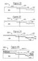
- FIG. 4Cis a cross-sectional view of a plurality of spring contact elements mounted to a component such as a space transformer, in use, probing (making temporary pressure connections with) another component such as a semiconductor device, according to the invention.
- FIG. 4Dis a cross-sectional view of another embodiment (compare FIG. 4B ) of a technique for mounting a plurality of spring contact elements to another component such as a space transformer, according to the invention.
- FIG. 4Eis a cross-sectional view of another embodiment (compare FIG. 4B ) of a technique for mounting a plurality of spring contact elements to another component such as a space transformer, according to the invention. This figure also illustrates another embodiment of a spring contact element, according to the invention.
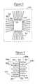
- FIG. 5is a schematic (stylized) plan view illustration of an application (use) for the spring contact elements of the present invention.
- FIG. 6is a schematic (stylized) plan view illustration of another application (use) for the spring contact elements of the present invention.
- FIG. 7Ais a cross-sectional view of another embodiment (compare. FIG. 4D ) of a technique for mounting a spring contact element to another component such as a space transformer, according to the invention.
- FIG. 7Bis a cross-sectional view of another embodiment (compare FIG. 7A ) of a technique for mounting a spring contact element to another component such as a space transformer, according to the invention.
- FIG. 7Cis a cross-sectional view of another embodiment (compare FIG. 7A ) of a technique for mounting a spring contact element to another component such as a space transformer, according to the invention.
- FIG. 7Dis a cross-sectional view of another embodiment (compare FIG. 7A ) of a technique for mounting a spring contact element to another component such as a space transformer, according to the invention.
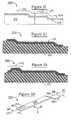
- FIG. 8Ais a perspective view of an alternate embodiment of a spring contact element (compare FIG. 3B ), omitting a showing of the sacrificial substrate, according to the invention.
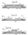
- FIG. 9Ais a side cross-sectional view of a first step in a technique for achieving controlled impedance in a spring contact element, according to the invention.
- FIG. 9Bis a side cross-sectional view of a next step in the technique for achieving controlled impedance in a spring contact element, according to the invention.
- FIG. 9Cis an end cross-sectional view of the controlled impedance spring contact element of FIG. 9B , according to the invention.
- a probe card assemblywhich includes elongate resilient (spring) contact elements mounted to a “space transformer” component.
- a space transformeris a multilayer interconnection substrate having terminals disposed at a first pitch on a one surface thereof and having corresponding terminals disposed at a second pitch on an opposite surface thereof, and is used to effect “pitch-spreading” from the first pitch to the second pitch.
- the free ends (tips) of the elongate spring contact elementsmake pressure connections with corresponding terminals on an electronic component being probed (e.g., tested).
- FIGS. 1A and 1Billustrate an elongate resilient (spring) contact element 100 that is suitable for attachment as a free-standing structure to an electronic component including, but not limited to, the space transformer of the aforementioned probe card assembly.
- the structure 100is elongate, has two ends 102 and 104 , central portion 106 therebetween, and has an overall longitudinal length of “L” between the two ends.
- the length “L”is in the range of 10-1000 mils, such as 40-500 mils or 40-250 mils, preferably 60-100 mils.
- the structurehas an effective length of “L”, less than “L”, which is the length over which the structure can flex in response to a force applied thereto.
- the end 102is a “base” whereat the contact element 100 will be mounted to an electronic component (not shown).
- the end 104is a “free-end” (tip) which will effect a pressure connection with another electronic component (e.g., a device-under-test, not shown).
- the contact element 100has an elongate “tail” portion extending beyond the base end 102 , opposite the central portion 106 .
- the structure 100has an overall height of “H”.
- the structureis “stepped”.
- the base portion 102is at a first height
- the tip 104is at another height
- a middle (central) portion 106is at a third height which is between the first and second heights. Therefore, the structure 100 has two “standoff” heights, labelled “d 1 ” and “d 2 ” in the figure.
- the spring contact element 100has two “steps”, a step up from the contact end 104 to the central body portion 106 , and a further step up from the central body portion 106 to the base end 102 .
- the structure 100is preferably provided with a “joining feature” 110 at its base portion 102 .
- the joining featuremay be a tab or, optionally a stud, which is used to facilitate brazing the probe structure to a substrate (e.g., a space transformer or a semiconductor device) during assembly therewith.
- a substratee.g., a space transformer or a semiconductor device
- the component or substrate to which the structure 100 is mountedmay be provided with a stud or the like to which the base portion 102 is mounted.
- the structure 100is intended to function as a cantilever beam, and is preferably provided with at least one taper angle, labelled “ ⁇ ” in FIG. 1B .
- the width “w 1 ” of the structure 100 at its base end 102is in the range of 5-20 mils, preferably 8-12 mils
- the width “w 2 ” of the structure 100 at its tip end 104in the range of 1-10 mils, preferably 2-8 mils
- the taper angle “ ⁇ ”is preferably in the range of 2-6 degrees.
- the width of the structure(hence, the taper angle “ ⁇ ”) is readily controlled employing well-known lithographic techniques.
- the tip end 104 of the structure 100is preferably provided with an integral protruding topological feature 108 , for example in the geometric form of a pyramid, to aid in effecting pressure connection to a terminal of an electronic component (not shown).
- the spring contact element 100is three-dimensional, extending in the x- y- and z-axes. Its length “L” is along, the y-axis, its widths (“w 1 ” and “w 2 ”) is along the x-axis, and its thicknesses (“t 1 ” and “t 2 ”) and height (“H”) are along the x-axis.
- Llength
- Wwidth
- w 2width
- Hheight
- FIG. 1Cillustrates a contact structure 150 similar in most respects to the structure 100 of FIGS. 1A and 1B .
- the structureis elongate, has a base end 152 (compare 102 ) and a tip end 154 (compare 104 ), and a topological feature 158 (compare 108 ) incorporated into its tip end.
- the principal difference being illustrated in FIG. 1Cis that the structure can be provided with a second taper angle “ ⁇ ”.
- the thickness “t 1 ” of the structure 100 at its base end 102is in the range of 1-10 mils, preferably 2-5 mils, and the thickness “t 2 ” of the structure 100 at its tip end 104 in the range of 1-10 mils, preferably 1-5 mils, and the taper angle “ ⁇ ” is preferably in the range of 2-6 degrees.
- the angle “ ⁇ ”may be created using various methods for controlling the thickness distribution. For example, if the structure 100 is formed by plating, a suitable plating shield can be incorporated into the bath. If the structure 100 is formed other than by plating, appropriate known processes for controlling the spatial distribution of thickness of the resulting structure would be employed. For example, sandblasting or electro-discharge machining (EDM) the structure 100 .
- EDMelectro-discharge machining
- the structuresuitably has a composite (dual) taper from its base end 102 to its tip end 104 . It has a taper angle “ ⁇ ” which, as will be evident from the description of a contact structure mounted to a component or substrate set forth hereinbelow, is parallel to the x-y plane of the substrate or component to which the contact structure 100 is mounted. And it has a has a taper angle “ ⁇ ” which represents a narrowing of the structure's cross section (z-axis).
- the contact elementis tapered to be wider and/or thicker at its contact end 104 than at its base end 102 , rather than narrower and/or thinner as described above. It is also possible that the contact element is provided with a plurality of different tapers, for example, tapering in (e.g., wider to narrower) from the base end to the central portion, then tapering back out (e.g., narrow to wider) towards the contact end.
- the contact structures 100 and 150are principally, preferably entirely, metallic, and may be formed (fabricated) as multilayer structures, as is described in greater detail hereinbelow. Suitable materials for the one or more layers of the contact structures include but are not limited to:
- goldespecially hard gold
- silverboth of which exhibit excellent current-carrying capabilities and good contact resistivity characteristics
- tin, lead, bismuth, indium and their alloyscan also be used.
- FIG. 1Dshows an enlarged view of the contact end 154 of the contact structure 150 (equally applicable to the contact ends of other contact structures illustrated herein).
- the contact feature 154is suitably quite prominent, projecting a distance “d 3 ”, in the range of 0.25-5 mils, preferably 3 mils from the bottom (as viewed) surface of the contact end of the spring contact element, and is suitably in the geometric shape of a pyramid, a truncated pyramid, a wedge, a hemisphere, or the like.
- the resulting spring contact elementhas an overall height “H” which is the sum of “d 1 ”, “d 2 ” (and “d 3 ”) plus the thickness of the central body portion.
- a exemplary spring contact elementsuitable for effecting connections between two electronic components, typically being mounted by its base end to a one of the two electronic components and effecting a pressure connection with its contact end to an other of the two electronic components, having the following dimensions (in mils, unless otherwise specified):
- “d 1 ”is a small fraction of “H”, such as between one-fifth and one-half the size of “H”;
- “w 2 ”is approximately one-half the size of “w 1 ”, and is a small fraction of “H”, such as between one-tenth and one-half the size of “H”;
- t 2is approximately one-half the size of “t 1 ”, such as between one-tenth and one-half the size of “H”.
- Another dimensionis of interest—namely, the width and length (i.e., footprint) of the overall tip end ( 104 ).
- the tip endis expected to make contact with a terminal of an electronic component which is recessed (e.g., a bond pad of a semiconductor device which has passivation material surrounding the bond pad)
- the contact feature ( 108 )is of sufficient height (d 3 ) to make contact with the recessed terminal.
- the selection of an appropriate tip end designwill be dictated by the peculiarities of the given application. For example, for contacting bond pads on silicon devices, the tip end design illustrated in FIG. 1D would likely be most appropriate. For contacting C 4 bumps, the tip end design illustrated in FIG. 1E (described hereinbelow) would likely be most appropriate.
- FIG. 1Eillustrates an alternate embodiment of the invention wherein discrete contact tip structures 168 , such as are described in the aforementioned PCT/US96/08107 can be mounted to the contact end portions 164 of the spring contact elements, such as by brazing 170 thereto. This provides the possibility of the contact tip structure 168 having a different metallurgy, than the spring contact element ( 150 ).
- the metallurgy of the spring contact element ( 150 )is suitably targeted at its mechanical (e.g., resilient, spring) characteristics and its general capability to conduct electricity, while the metallurgy of a contact tip structure 168 mounted thereto is appropriately targeted to making superior electrical connection with a terminal (see, e.g., 420 , hereinbelow) of an electronic component (see, e.g., 422 , hereinbelow) being contacted and, if needed, can have superior wear-resistance.
- a terminalsee, e.g., 420 , hereinbelow
- an electronic componentsee, e.g., 422 , hereinbelow
- a contact element such as that described hereinabovewould be difficult, to punch out of a foil of spring material and mount in a precise location on an electronic component such as a space transformer, at the scale (dimensions) described herein.
- processessuch as photolithography are employed to fabricate the spring contact elements of the present invention with tolerances, both of the springs themselves and with regard to the relative locations of a plurality of springs, suitable for use as interconnections in the context of fine-pitch microelectronics.
- FIGS. 2A-2Jillustrates an exemplary process 200 for fabricating the aforementioned resilient contact structures 100 ( 150 ).
- the present inventionis not limited to this exemplary process.
- a blanket layer 204 of silicon nitride (“nitride”)is applied to the surface of the sacrificial substrate.
- This layer 204will act as an etch stop in subsequent steps of the process.
- a layer 206 of a masking material, such as photoresist,is applied over the nitride layer 204 , and is imaged and developed using conventional photolithographic techniques (e.g., actinic light passing through a mask).
- the sacrificial substrateis a material selected from the group consisting of silicon, aluminum, copper, ceramic, and the like.
- the sacrificial substratecan also be a “clad” (multilayer) structure, such as copper-invar-copper or aluminum-alumina-aluminum, and preferably has a coefficient of thermal expansion which matches that of the component to which the contact structures are ultimately mounted.
- a cladmultilayer
- vis-a-vis the “machining” of the sacrificial substrateis applicable to sacrificial substrates which are silicon.
- the sacrificial substratecan be formed of titanium-tungsten which is readily etched with hydrogen peroxide.
- an opening 210 to the surface of the sacrificial substrate 202can be created through both of the layers 206 and 204 , as illustrated in FIG. 2C .
- the surface of the sacrificial substrateis exposed.
- the surface of the sacrificial substrateis covered by the residual (remaining) portions 204 a and 206 a of the layers 204 , 206 , respectively, that are not removed by etching.
- selected portions of the photoresist 206can be removed employing other techniques, such as known techniques involving lasers, E-beam, and the like, and the resulting exposed (no longer covered) portions of the nitride layer 204 can be removed using chemical etching processes, the result of which is that an opening 210 to the surface of the sacrificial substrate 202 can be created, as illustrated in FIG. 2C .
- Using a laser to remove portions of the masking layer 206 (other portions 206 a being remaining portions)provides the possibility of having more carefully-controlled aspect ratios for the resulting openings 210 , for example, obtaining steeper and deeper, more-vertical sidewalls in the opening.
- the sacrificial substrate 202is etched in the openings 210 through the nitride layer 204 , using known chemistry for selectively etching the substrate.
- a silicon substratecan selectively be etched (with respect to nitride) using potassium hydroxide (KOH). This will create a trench 220 in the substrate 202 , the depth of which is controlled to correspond to the aforementioned standoff height “d 2 ” (see FIG. 1A ).
- the sidewall 222 of the trenchwill favorably exhibit a non-vertical angle “ ⁇ ”, such as 54.74° (rather than)90°, as may be inherent in and controlled by the crystalline structure of the substrate.
- ⁇such as 54.74° (rather than)90°
- a silicon substrate having a (100) crystal orientation when etchedwill etch in the (111) planes.
- the residual portion 204 a of the etch stop layer 204is preferably removed.
- a next step of the process 200illustrated in FIG. 2E , the previous steps illustrated and described with respect to FIGS. 2A-2D are repeated, to create another trench 230 in the sacrificial substrate 202 that is longitudinally offset from and contiguous with the trench 220 .
- the trench 230can be formed in an end portion (right hand side, as viewed) of the previously-formed trench 220 .
- an etch stop layer 224(compare 204 ) is applied, a masking layer (not shown, compare 206 ) is applied over the etch stop layer, an opening is created through the masking layer and the etch stop layer, and the substrate is etched.
- a next step of the process 200illustrated in FIG. 2F , the previous steps illustrated and described with respect to FIGS. 2A-2D are repeated, to create a small geometric intrusion (depression) 240 (compare “d 3 ” of FIG. 1D ) in the sacrificial substrate 202 in the bottom of the second trench 230 .
- intrusionis selected as being the complement to “negative of” the resulting protruding feature ( 108 ) that will be fabricated on the resulting spring contact element.
- the feature 240could also be considered to be a “depression”, a “recess”, an “indentation” or an “intaglio”.) Namely, an etch stop layer 234 (compare 204 , 224 ) is applied, a masking layer (not shown, compare 206 ) is applied over the etch stop layer, a small opening is created through the masking layer and the etch stop layer, and the substrate is etched.
- the shape of the intrusion 240is suitably that of an inverted (as viewed) pyramid and, as mentioned hereinabove, may suitably have sides at the crystalline angle of silicon.
- this intrusion 240will define the topological feature 108 present on the tip of the contact structure 100 described hereinabove (pyramid, truncated pyramid, etc.). Finally, the nitride layer 234 is removed.
- Each of the trenches 220 and 230can be considered to be a “subtrench” of a larger overall trench which also includes the depression 240 .
- FIGS. 2A-2Fdescribe the preparation of a sacrificial substrate for the fabrication of resilient contact structures thereon. It is within the scope of this invention that certain of the steps described hereinabove could be performed in other than the recited order.
- the trench 230could be formed prior to forming the trench 220 .
- the process described hereinabovecould be carried out on a silicon wafer that has active devices already formed therein.
- the forming of trenches ( 220 and 230 ) and features ( 240 )could well destroy the active devices unless (i) they were to be formed at areas of the wafer that do not contain active devices, or (ii) the spring contact elements were fabricated on a sacrificial substrate then attached to active devices (see e.g., FIGS. 4A-4B hereinbelow), or (iii) a layer of material suitable for performing the function of the sacrificial substrate ( 202 ) described hereinabove is first applied to the surface of the wafer.
- the layers 252 and 254constitute a “release mechanism” which is incorporated into the sacrificial substrate which, in use, permits the sacrificial substrate to be removed after the spring contact elements fabricated thereon (as described hereinbelow) are mounted to the terminals of the electronic component.
- a masking layer 258(compare 206 ), such as photoresist, is applied to the substrate and is patterned to have an openings 260 corresponding to the length “L” and width (“w 1 ” and “w 2 ”, and widths therebetween) of the desired resulting spring contact element (see FIGS. 1A and 1B ).
- a relatively thick “structural” metallic layer 256is deposited within the openings 260 , using any suitable process such as electroplating of a suitable material such as nickel, atop the previously applied layers 252 and 254 . This layer 256 is intended to control (dominate) the mechanical characteristics of the resulting spring contact element ( 100 ).
- the opening 260includes the trench 220 , the trench 230 , the depression 240 and a portion of the substrate 202 which is adjacent and contiguous with the first trench 220 .
- An exemplary average ((t 1 +t 2 )/2) thickness for this layer 256is 1-10 mils, preferably 1-5 mils.
- Suitable materials for the layer 256such as nickel and its alloys, have been set forth hereinabove.
- the masking layer 258is removed, exposing the layers 252 and 254 .
- These layersare suitably selectively chemically etched, so that all that remains on the substrate is an elongate structure 270 (compare 100 ) having a one end 272 (compare 102 ), an other end 274 (compare 104 ), a central portion 276 (compare 106 ) and a raised topological feature 278 (compare 108 ) at its end 274 .
- This elongate structure 270is the resulting spring contact element.
- FIG. 2Jis another cross-sectional view of the resulting structure 270 , still resident upon the substrate, with the layers 252 and 254 omitted, for illustrative clarity. The similarity between this structure 270 and the spring contact element 100 of FIG. 1A is readily apparent.
- a sacrificial substratecan be prepared with a single very wide set of trenches, ( 220 , 230 , 240 ), then deposit the metals ( 252 , 254 , 256 ), then perform an additional final masking and etching step to define the individual contact elements.
- a processwould look similar to the process described hereinabove with respect to FIGS. 2A-2G , followed by blanket deposition of the metal ( 256 ) layers, followed by masking and etching to define the individual contact elements.
- FIGS. 3A and 3Billustrate another one of many possible embodiments for a contact structure 300 fabricated by the techniques described hereinabove.
- a somewhat truncated-pyramidal joining feature (stud) 310is fabricated as an attachment feature at the base portion 304 of the contact structure 300 .
- this stud 310will allow for some misalignment tolerance during assembly.
- the remaining portions of the contact structure 300are comparable to those described hereinabove with respect to the contact structure 270 -namely, a central main body portion 306 (compare 276 ), a contact end portion 304 (compare 274 ), and a feature 308 (compare 278 ).
- a plurality of contact structurese.g., 270 fabricated upon a sacrificial substrate (e.g., 202 ) can be mounted (affixed) to another substrate or to an electronic component such as a space transformer.
- FIG. 4Aillustrates a technique 400 wherein a plurality (two of many shown) of contact structures 402 (compare 100 , 150 , 270 , 300 ) have been fabricated on a sacrificial substrate 404 (compare 202 ).
- the base end portions (compare 310 ) of the contact structures 402are brought into contact with a corresponding plurality of terminals 406 on an electronic component 408 such as the aforementioned space transformer of a probe card assembly, whereupon the base end portions are suitably soldered or brazed 410 to the terminals 406 .
- any suitable technique and/or material for affixing the base end portions of the contact structures ( 402 ) to terminals of an electronic componentbe employed, including brazing, welding (e.g., spot welding), soldering, conductive epoxy, tacking the contact structure in any suitable manner to the terminal and securely affixing the contact structure to the terminal by plating (e.g., electroplating), and the like.
- a plurality of elongate spring contact elementscan be mounted to an electronic component having a plurality of terminals on a surface thereof.
- Each spring contact elementhas a base end and a contact end opposite the base end, and is mounted by its base end to a corresponding terminal of the electronic component.
- the contact end of each spring contact elementextends above the surface of the electronic component to a position which is laterally offset from its base end.
- FIG. 4Done trench 442 is illustrated extending under a plurality (two of many shown) spring contact elements. It is within the scope of this invention that there is a single discrete trench under each of the plurality of spring contact elements ( 450 ) structures mounted to an electronic component ( 444 ).
- FIG. 4Eillustrates an alternate embodiment of the present invention wherein a spring contact element 460 is mounted to an electronic component 470 (compare 444 ) via a stud 472 extending from a surface of the electronic component 470 .
- the base end 462 of the spring contact element 460is suitably brazed to the stud 472 .
- the stud 472suitably has a height in the range of 3-4 mils.
- the contact end portion 464(compare 104 ) preferably remains offset by a distance “d 1 ” from the central body portion 466 .
- d 1a distance from the central body portion 466 .
- FIG. 4Fillustrates another embodiment of the invention wherein the spring contact element (contact structure) 480 is formed without any step or offset (rather than one or two steps).
- the offset of the base end portion 482 from the central body portion 486(compare “d 2 ” in FIG. 1A ) is ZERO, and the base end portion 482 is coplanar with the central body portion 486 . Since there is no offset at the base end portion, the base end 482 is mounted to a stud 492 on the surface of the electronic component 490 so that the body portion 486 is elevated above the surface of the component 490 .
- the offset of the contact end portion 484 (compare 104 ) from the central body portion 486(compare “d 1 ” in FIG.
- a prefabricated contact tip structure 488(compare 168 ) may be affixed (e.g., joined, such as by brazing) to the contact end 484 so that the body portion 486 will be spaced away from a component (not shown, compare 420 ) being contacted by the contact structure 480 .
- FIG. 5illustrates an application wherein a plurality of spring contact elements 500 such as those described hereinabove are arranged on a substrate such as a space transformer, and affixed thereto in the manner described hereinabove, so that their contact ends are disposed in a manner suitable for making contact with the bond pads of a semiconductor device having its bond pads arranged along its periphery.
- a plurality of spring contact elements 500such as those described hereinabove are arranged on a substrate such as a space transformer, and affixed thereto in the manner described hereinabove, so that their contact ends are disposed in a manner suitable for making contact with the bond pads of a semiconductor device having its bond pads arranged along its periphery.
- FIG. 6illustrates another application wherein a plurality of spring contact elements 600 such as those described hereinabove are arranged on a substrate such as a space transformer, and affixed thereto in the manner described hereinabove, so that their contact ends are disposed in a manner suitable for making contact with the bond pads of a semiconductor device having its bond pads arranged in a row along a centerline thereof.
- a plurality of spring contact elements 600such as those described hereinabove are arranged on a substrate such as a space transformer, and affixed thereto in the manner described hereinabove, so that their contact ends are disposed in a manner suitable for making contact with the bond pads of a semiconductor device having its bond pads arranged in a row along a centerline thereof.
- Each spring contact element(compare 100 ), generally denoted by the reference numeral 600 , has a base end 602 (compare 102 ) and a contact end 604 (compare 104 ), and are mounted to an electronic component such as a space transformer component (schematically illustrated by the dashed line 610 ) of a probe card assembly (not shown).
- the contact ends 604are arranged close to one another, in a pattern mirroring that of the bond pads 622 (illustrated schematically by circles) of an electronic component (schematically illustrated by the dashed line 620 ) such as a semiconductor device.
- the spring contact elements 600are arranged in the following sequence:
- the showing of only two different-length contact structuresis merely exemplary and it should be understood that it is within the scope of this invention that a plurality of spring contact elements having more than two different lengths can be disposed on a common substrate.
- the showing of only two different-length contact structuresis merely exemplary.
- FIGS. 5 and 6may be used to generate a plurality of probes (spring contact elements) in any arrangement required for probing of either peripheral or lead-on-center (LOC) devices.
- LOClead-on-center
- the spring constants of a plurality of spring elements exhibiting different spring constantscan be adjusted (tailored), on an individual basis, to make them more uniform with one another.
- FIG. 7Aillustrates a technique for tailoring spring constant.
- a spring contact element 700(compare 450 ) is mounted by its base end 702 (compare 452 ) to an electronic component 710 (compare 444 ).
- a trench 712(compare 442 ) is formed in the surface of the electronic component 710 and extends from under the contact end 704 (compare 454 ) of the spring contact structure 700 , along the body portion 706 (compare 456 ) thereof, towards the base end 702 of the spring contact element 700 to a position (point) “P” which is located a prescribed, fixed distance, such as 60 mils from the contact end 704 .
- the entire spring contact element 700When a force is applied downwards to the contact end 704 , the entire spring contact element 700 will bend (deflect) until the body portion 706 contacts the end of the trench 712 at the point “P”, whereupon only the outermost portion (from the point “P” to the end 704 ) of the spring contact element is permitted to deflect.
- the outermost portion of the spring contact elementhas an ‘effective’ length of “L 1 ”.
- the outermost portion of the spring contact elementhas an ‘effective’ length of “L 1 ”. In this manner, the reaction to applied contact forces can be made uniform among spring contact elements of various lengths (so long as the point “P” falls somewhere within the central body portion of the spring contact element).
- FIG. 7Billustrates another technique for tailoring spring constant.
- a spring contact element 720(compare 450 ) is mounted by its base end 702 (compare 452 ) to an electronic component 710 (compare 444 ).
- a structure 732(compare 712 ) is formed on the surface of the electronic component 730 (compare 710 ) at a location between the base end 722 of the spring contact structure 720 , between the surface of the electronic component 730 and the central body portion 726 (compare 706 ) of the spring contact element 720 and extends along the body portion 726 (compare 706 ) thereof, towards the contact end 724 of the spring contact element 720 to a position (point) “P” which is located a prescribed, fixed distance, such as the aforementioned (with respect to FIG.
- the structureis suitably a bead of any hard material, such as glass or a pre-cut ceramic ring, disposed on the surface of the electronic component 730 .
- a forceis applied downwards to the contact end 724 , only the outermost portion (from the point “P” to the end 724 ) of the spring contact element is permitted to deflect.
- the reactions to applied contact forcescan be made uniform among spring contact elements of various lengths.
- FIG. 7Cillustrates yet another technique for tailoring spring constant.
- a spring contact element 740(compare 720 ) is mounted by its base end 742 (compare 722 ) to an electronic component 750 (compare 730 ).
- An encapsulating structure 752(compare 732 ) is formed on the surface of the electronic component 750 in a manner similar to the structure 732 of the previous embodiment. However, in this case, the structure 752 fully encapsulates the base end 742 of the spring contact structure 740 and extends along the body portion 746 (compare 726 ) thereof, towards the contact end 744 thereof, to a position (point) “P” Which is located a prescribed, fixed distance, such as the aforementioned (with respect to FIG.
- the outermost portion of the spring contact elementhas an ‘effective’ length of “L 1 ”.
- L 1the length of the spring contact element
- FIG. 7Dillustrates yet another technique for tailoring spring constant.
- a spring contact element 760(compare 740 ) is mounted by its base end 762 (compare 742 ) to an electronic component 770 (compare 750 ).
- the body portion 766is formed with a “kink” 772 at a position (point) “P” which is located a prescribed, fixed distance, such as the aforementioned (with respect to FIG. 7C prescribed distance, from the contact end 764 .
- the outermost portion of the spring contact elementhas an ‘effective’ length of “L 1 ”.
- the reactions to applied contact forcescan be made uniform among spring contact elements of various lengths.
- the spring contact elements illustrated and described hereinabovehave been elongate and linear (disposed along the y-axis), generally best suited to accommodate movement (deflection) in the z-axis (i.e., normal to the component or substrate to which they are mounted).
- FIG. 8Aillustrates a spring contact element 800 that has been fabricated according to the techniques set forth hereinabove, with the exception (noticeable difference) that the central body portion 806 (compare 106 ) of the contact element is not straight, Although it may still lay in a plane (e.g., the x-y plane), it is illustrated as jogging along the x-axis while traversing the y-axis, in which case the base end 802 (compare 102 ) will have a different x-coordinate than the contact end 804 (compare 104 ) or the contact feature 808 (compare 108 ) disposed at the contact end 804 .
- a planee.g., the x-y plane
- the spring contact elementFor use in probing semiconductor devices, particularly at speed testing, it is advantageous that the spring contact element have controlled impedance.
- FIGS. 9A-9Cillustrate a technique 900 for achieving controlled impedance in a spring contact element, according to the invention.
- the tip end 904 of the spring contact elementis masked (not shown), and a suitable thin (e.g., 1-10 ⁇ m) insulating layer 920 , such as parylene, is deposited, such as by vapor deposition, onto all but the tip end 904 of the spring contact element, and adjacent surface of the electronic component.
- a suitable thin (e.g., 1-10 ⁇ m) insulating layer 920such as parylene
- the conductive layer 922is suitably connected to ground to function as a ground plane and control the impedance of the resulting spring contact element.
- the component 910is provided with a second terminal 914 which is electrical ground.
- This terminal 914is suitably masked along with the tip end 904 of the spring contact element prior to applying the insulating layer 920 , so that the subsequent conductive layer 922 will also deposit thereon and be connected thereto.
- this thicknesses of the layers 920 and 922need only be sufficient to be continuous, and to provide the sought after controlled impedance, and should not be so thick as to interfere with the mechanical operation of the spring contact element.
- the representations in FIGS. 9B and 9Care not drawn to scale.
- the resulting spring contact elementsmay be heat-treated to enhance their mechanical characteristics, either while they are resident upon the sacrificial substrate or after they are mounted to another substrate or an electronic component.
- any heat incident to mounting (e.g., by brazing) the spring contact elements to a componentcan advantageously be employed to “heat treat” the material of the spring contact element.
- a comparable spring contact elementcould be fabricated without etching into the sacrificial substrate, by disposing multiple layers of photoresist (masking material) onto a substrate, forming openings therein, seeding the opening for electroplating or the like, building up a metallic mass within the opening, and removing the photoresist.
- photoresistmasking material
- the contact structurecan be fabricated on or attached to active semiconductor devices.
Landscapes
- Physics & Mathematics (AREA)
- General Physics & Mathematics (AREA)
- Engineering & Computer Science (AREA)
- Condensed Matter Physics & Semiconductors (AREA)
- Manufacturing & Machinery (AREA)
- Computer Hardware Design (AREA)
- Microelectronics & Electronic Packaging (AREA)
- Power Engineering (AREA)
- Measuring Leads Or Probes (AREA)
Abstract
Description
This patent application is division of U.S. patent application Ser. No. 11/456,568, filed Jul. 11, 2006) (now U.S. Pat. No. 7,601,039), which is a continuation of U.S. patent application Ser. No. 09/753,310, filed Dec. 29, 2000 (now U.S. Pat. No. 7,073,254), which is a division of U.S. patent application Ser. No. 08/802,054, filed Feb. 18, 1997 (now U.S. Pat. No. 6,482,013), which claims the benefit of the following U.S. Patent Application Nos.:
60/034,053 filed 31 Dec. 96;
60/012,027 filed 21 Feb. 96;
60/005,189 filed 17 May 96; and
60/024,555 filed 26 Aug. 96.
The present invention relates to resilient electrical contact (interconnection) elements (structures), also referred to as spring contacts, suitable for effecting pressure connections between electronic components and, more particularly, to microminiature spring contacts such as may be used in probing (resiliently and temporarily contacting) microelectronic components such as active semiconductor devices.
Commonly-owned U.S. patent application Ser. No. 08/152,812 filed 16 Nov. 93 (now U.S. Pat. No. 4,576,211, issued 19 Dec. 95), and its counterpart commonly-owned copending “divisional” U.S. patent application Ser. No. 08/457,479 filed 1 Jun. 95 (status: pending) and 08/570,230 filed 11 Dec. 95 (status: pending), all by KHANDROS, disclose methods for making resilient interconnection elements for microelectronics applications involving mounting an end of a flexible elongate core element (e.g., wire “stem” or “skeleton”) to a terminal on an electronic component coating the flexible core element and adjacent surface of the terminal with a “shell” of one or more materials having a predetermined combination of thickness, yield strength and elastic modulus to ensure predetermined force-to-deflection characteristics of the resulting spring contacts. Exemplary materials for the core element include gold. Exemplary materials for the coating include nickel and its alloys. The resulting spring contact element is suitably used to effect pressure, or demountable, connections between two or more electronic components, including semiconductor devices.
Commonly-owned, copending U.S. patent application Ser. No. 08/340,144 filed 15 Nov. 94 and its corresponding PCT Patent Application No. PCT/US94/13373 filed 16 Nov. 94 (WO95/14314, published 26 May 95), both by KHANDROS and MATHIEU, disclose a number of applications for the aforementioned spring contact element, and also disclosed techniques for fabricating contact pads at the ends of the spring contact elements. For example, inFIG. 14 thereof, a plurality of negative projections or holes, which may be in the form of inverted pyramids ending in apexes, are formed in the surface of a sacrificial layer (substrate). These holes are then filled with a contact structure comprising layers of material such as gold or rhodium and nickel. A flexible elongate element is mounted to the resulting contact structure and can be overcoated in the manner described hereinabove. In a final step, the sacrificial substrate is removed. The resulting spring contact has a contact pad having controlled geometry (e.g., sharp points) at its free end.
Commonly-owned, copending U.S. patent application Ser. No. 08/452,255 filed 26 May 95 and its corresponding PCT Patent Application No. PCT/US95/14909 filed 13 Nov. 95 (WO96/17278, Published 6 Jun. 96), both by ELDRIDGE, GRUBE, KHANDROS and MATHIEU, disclose additional techniques and metallurgies for fabricating contact tip structures on sacrificial substrates, as well as techniques for transferring a plurality of spring contact elements mounted thereto, en masse, to terminals of an electronic component (see, e.g.,FIGS. 11A-11F and12A-12C therein).
Commonly-owned, copending U.S. Provisional Patent Application No. 60/005,189 filed 17 May 96 and its corresponding PCT Patent Application No. PCT/US96/08107 filed 24 May 96 (WO96/37332, published 28 Nov. 96), both by ELDRIDGE, KHANDROS, and MATHIEU, discloses techniques whereby a plurality of contact tip structures (see, e.g, #620 inFIG. 6B therein) are joined to a corresponding plurality of elongate contact elements (see, e.g., #632 ofFIG. 6D therein) which are already mounted to an electronic component (#630). This patent application also discloses, for example inFIGS. 7A-7E therein, techniques for fabricating “elongate” contact tip structures in the form of cantilevers. The cantilever tip structures can be tapered, between one end thereof and an opposite end thereof. The cantilever tip structures of this patent application are suitable for mounting to already-existing (i.e., previously fabricated) raised interconnection elements (see, e.g., #730 inFIG. 7F ) extending (e.g., free-standing) from corresponding terminals of an electronic component (see. e.g., #734 inFIG. 7F ).
Commonly-owned, copending U.S. Provisional Patent Application No. 60/024,555 filed 26 Aug. 96, by ELDRIDGE, KHANDROS and MATHIEU, discloses, for example atFIGS. 2A-2C thereof, a technique whereby a plurality of elongate tip structures having different lengths than one another can be arranged so that their outer ends are disposed at a greater pitch than their inner ends. Their inner, “contact” ends may be collinear with one another, for effecting connections to electronic components having terminals disposed along a line, such as a centerline of the component.
The present invention addresses and is particularly well-suited to making interconnections to modern microelectronic devices having their terminals (bond pads) disposed at a fine-pitch. As used herein, the term “fine-pitch” refers to microelectronic devices that have their terminals disposed at a spacing of less than 5 mils, such as 2.5 mils or 65 μm. As will be evident from the description that follows, this is preferably achieved by taking advantage of the close tolerances that readily can be realized by using lithographic rather than mechanical techniques to fabricate the contact elements.
An object of the present invention is to provide an improved technique for fabricating spring contact elements.
Another object of the invention is to provide a technique for fabricating spring contact elements using processes that are inherently well-suited to the fine-pitch close-tolerance world of microelectronics.
Another object of the invention is to provide a technique for fabricating spring contact elements that are suitable for probing electronic components such as semiconductor devices, and that is readily scaleable to probing fine-pitch peripheral interconnect structures.
Another object of the invention is to provide a technique for fabricating spring contact elements that are suitable for socketing electronic components such as semiconductor devices, such as for performing burn-in on said devices.
According to the invention, an elongate spring contact element suitable for microelectronic applications is fabricated by forming depressions (such as trenches, such as by etching) in a sacrificial substrate and depositing (such as by plating) metallic materials into the depressions. A plurality of spring contact elements may be fabricated in this manner on a single sacrificial substrate, with lithographically-defined tolerances (e.g., dimensions, spacings).
The resulting spring contact elements may then be mounted to another substrate such as a passive substrate or an active substrate such as a semiconductor device, after which the sacrificial substrate is removed.
An exemplary spring contact element formed in this manner has a length “L” between its base end and its contact end. The base end is preferably offset in a first direction from a central portion of the spring contact element, and the contact end is preferably offset in an opposite direction from the central portion. In this manner, the overall spring contact element is not planar and, when its base end is mounted to an electronic component, its contact end extends above the surface of the electronic component to which it is mounted.
An exemplary sacrificial substrate upon which the spring contact elements may be fabricated is a silicon wafer, in which case the process of the present invention advantageously utilizes the directionally selective etching of silicon used for micro-machining processes to create an electroform which is used to place up the final spring contact element. This approach may optionally employ laser-based ablation of photoresist, as opposed to lithographic development of the photoresist, in order to create the high aspect ratio of width to height which is required for fine pitch spacings between the spring contact elements.
An exemplary application for the spring contact elements of the present invention is as probe elements used to effect pressure connections between a substrate and a device-under-test (DUT), in which case the spring contact elements are suitably mounted to a space transformer component of a probe card assembly, such as is described in the aforementioned Ser. No. 08/554,902 and PCT/US95/14844. Alternatively, the spring contact elements are mounted to and extend from an active electronic component such as an application specific integrated circuit (ASIC).
The spring contact element is suitably formed of at least one layer of a metallic material selected for its ability to cause the resulting contact structure to function, in use, as a spring (i.e., exhibit elastic deformation) when force is applied to its contact (free) end.
The resulting spring contact element is preferably “long and low”, having:
- a length “L”, as measured from one end to another end;
- a height “H” measured transverse the length in a direction that is normal (z-axis) to the surface of the sacrificial substrate (and, normal to the component to which the spring contact element is ultimately mounted);
- a contact end portion which is offset in a one direction (e.g., negative along the z-axis) from a central portion of the spring element by a distance “d1”; and
- a base end portion which is offset in one direction (e.g., positive z-axis) from the central portion of the spring element by a distance. “d2”.
The spring contact element is preferably tapered from the one (base) end to the other (contact) end thereof, the spring contact element having the following dimensions:
- a width “w1” at its base end as measured parallel to the surface of the sacrificial substrate and transverse to the longitudinal axis of the spring element;
- a width “w2” at its contact end as measured parallel to the surface of the sacrificial substrate and transverse to the longitudinal axis of the spring element;
- a thickness “t1” at its base end, measured along the z-axis; and
- a thickness “t2” at its contact end, measured along the z-axis; resulting in:
- a widthwise taper angle “α” (alpha); and
- a thickness taper angle “β” (beta).
The spring contact element is also suitably provided with a projecting feature at its contact end, said feature having a dimension “d3” measured along the z-axis.
There is thus described herein an exemplary spring contact element suitable for effecting connections between two electronic components, typically being mounted by its base end to a one of the two electronic components and effecting a pressure connection with its contact end (e.g., by the projecting feature) to an other of the two electronic components, having the following dimensions (in mils, unless otherwise specified):
| dimension | range | preferred | ||
| L | 10-1000 | 60-100 | ||
| H | 4-40 | 5-12 | ||
| d1 | 3-15 | 7 ± 1 | ||
| d2 | 0-15 | 7 ± 1 | ||
| d3 | 0.25-5 | 3 | ||
| w1 | 3-20 | 8-12 | ||
| w2 | 1-10 | 2-8 | ||
| t1 | 1-10 | 2-5 | ||
| t2 | 1-10 | 1-5 | ||
| α | 0-30° | 2-6° | ||
| β | 0-30° | 0-6° | ||
Other objects, features and advantages of the invention will become apparent in light of the following description thereof.
Reference will be made in detail to preferred embodiments of the invention, examples of which are illustrated in the accompanying drawings. The drawings are intended to be illustrative, not limiting.
Although the invention will be described in the context of these preferred embodiments, it should be understood that it is not intended to limit the spirit and scope of the invention to these particular embodiments.
Certain elements in selected ones of the drawings are illustrated not-to-scale, for illustrative clarity.
Often, similar elements throughout the drawings are referred to by similar references numerals. For example, the element199 may be similar in many respects to the element299 in another figure. Also, often, similar elements are referred to with similar numbers in a single drawing. For example, a plurality of elements199 may be referred to as199a,199b,199c, etc.
Commonly-owned, copending U.S. patent application Ser. No. 08/554,902 filed 9 Nov. 95 and its corresponding PCT Patent Application No. PCT/US95/14844 filed 13 Nov. 95 (WO96/15458, published 23 May 96), both by ELDRIDGE, GRUBE, KHANDROS and MATHIEU, disclose a probe card assembly which includes elongate resilient (spring) contact elements mounted to a “space transformer” component. As used herein, a space transformer is a multilayer interconnection substrate having terminals disposed at a first pitch on a one surface thereof and having corresponding terminals disposed at a second pitch on an opposite surface thereof, and is used to effect “pitch-spreading” from the first pitch to the second pitch. In use, the free ends (tips) of the elongate spring contact elements make pressure connections with corresponding terminals on an electronic component being probed (e.g., tested).
Elongate, Resilient Cantilever-Like Contact Element
Thestructure 100 is elongate, has twoends central portion 106 therebetween, and has an overall longitudinal length of “L” between the two ends. The length “L” is in the range of 10-1000 mils, such as 40-500 mils or 40-250 mils, preferably 60-100 mils. As will become apparent from the discussion that follows, in use the structure has an effective length of “L”, less than “L”, which is the length over which the structure can flex in response to a force applied thereto.
Theend 102 is a “base” whereat thecontact element 100 will be mounted to an electronic component (not shown). Theend 104 is a “free-end” (tip) which will effect a pressure connection with another electronic component (e.g., a device-under-test, not shown). Although not illustrated, it is also possible that thecontact element 100 has an elongate “tail” portion extending beyond thebase end 102, opposite thecentral portion 106.
Thestructure 100 has an overall height of “H”. The height “H” is in the range of 4-40 mils, preferably 5-12 mils. (1 mil=0.001 inches)
As best viewed inFIG. 1A , the structure is “stepped”. Thebase portion 102 is at a first height, thetip 104 is at another height, and a middle (central)portion 106 is at a third height which is between the first and second heights. Therefore, thestructure 100 has two “standoff” heights, labelled “d1” and “d2” in the figure. In other words, thespring contact element 100 has two “steps”, a step up from thecontact end 104 to thecentral body portion 106, and a further step up from thecentral body portion 106 to thebase end 102.
In use, the standoff height “d1”, which is the “vertical” (as viewed inFIG. 1A ) distance between thetip 104 and thecentral portion 106, performs the function of preventing bumping of the structure (contact element) with a surface of a component being contacted by thetip end 104.
In use, the standoff height “d2”, which is the “vertical” (as viewed inFIG. 1A ) distance between the base102 and thecentral portion 106; performs the function of allowing the beam (contact element) to bend through the desired overtravel.
The dimensions for the standoff heights “d1” and “d2” are
- “d1” is in the range of 3-15 mils, preferably approximately 7 mils+1 mil; and
- “d2” is in the range of 0-15 mils, preferably approximately 7 mils+1 mil. In the case of “d2” being 0 mil, the structure would be substantially planar (without the illustrated step) between the
central portion 106 and thebase portion 102.
As best viewed inFIG. 1B , thestructure 100 is preferably provided with a “joining feature”110 at itsbase portion 102. The joining feature may be a tab or, optionally a stud, which is used to facilitate brazing the probe structure to a substrate (e.g., a space transformer or a semiconductor device) during assembly therewith. Alternatively, the component or substrate to which thestructure 100 is mounted may be provided with a stud or the like to which thebase portion 102 is mounted.
In use, thestructure 100 is intended to function as a cantilever beam, and is preferably provided with at least one taper angle, labelled “α” inFIG. 1B . For example, the width “w1” of thestructure 100 at itsbase end 102 is in the range of 5-20 mils, preferably 8-12 mils, and the width “w2” of thestructure 100 at itstip end 104 in the range of 1-10 mils, preferably 2-8 mils, and the taper angle “α” is preferably in the range of 2-6 degrees. The narrowing of (taper) thestructure 100, from itsbase 102 to itstip 104, permits controlled flexure and more even stress distribution (versus concentration) of thestructure 100 when itsbase 102 is secured (immovable) and a force is applied at its tip (104).
As will be evident in the discussion presented hereinbelow, the width of the structure (hence, the taper angle “α”) is readily controlled employing well-known lithographic techniques.
Thetip end 104 of thestructure 100 is preferably provided with an integral protrudingtopological feature 108, for example in the geometric form of a pyramid, to aid in effecting pressure connection to a terminal of an electronic component (not shown).
As illustrated inFIGS. 1A and 1B , thespring contact element 100 is three-dimensional, extending in the x- y- and z-axes. Its length “L” is along, the y-axis, its widths (“w1” and “w2”) is along the x-axis, and its thicknesses (“t1” and “t2”) and height (“H”) are along the x-axis. As will become evident in the discussion set forth hereinbelow (see, e.g.,FIG. 4B ), when thespring contact element 100 is mounted to an electronic component, it is mounted thereto so that the length and width of the spring contact element are parallel to the surface of the electronic component, and its height is normal to the surface of the electronic component.
As best viewed inFIG. 1C , the thickness “t1” of thestructure 100 at itsbase end 102 is in the range of 1-10 mils, preferably 2-5 mils, and the thickness “t2” of thestructure 100 at itstip end 104 in the range of 1-10 mils, preferably 1-5 mils, and the taper angle “β” is preferably in the range of 2-6 degrees.
The angle “β” (FIG. 1C ) may be created using various methods for controlling the thickness distribution. For example, if thestructure 100 is formed by plating, a suitable plating shield can be incorporated into the bath. If thestructure 100 is formed other than by plating, appropriate known processes for controlling the spatial distribution of thickness of the resulting structure would be employed. For example, sandblasting or electro-discharge machining (EDM) thestructure 100.
Thus, the structure suitably has a composite (dual) taper from itsbase end 102 to itstip end 104. It has a taper angle “α” which, as will be evident from the description of a contact structure mounted to a component or substrate set forth hereinbelow, is parallel to the x-y plane of the substrate or component to which thecontact structure 100 is mounted. And it has a has a taper angle “β” which represents a narrowing of the structure's cross section (z-axis).
It is within the scope of this invention that the structure is not tapered in width, in which case the taper angle “α” would be ZERO. It is also within the scope of this invention that the taper angle “α” is greater than 2-6 degrees, for example as much as 30 degrees. It is within the scope of this invention that the structure is not tapered in thickness, in which case the taper angle “β” would be ZERO. It is also within the scope of this invention that the taper angle “β” is greater than 2-6 degrees, for example as much as 30 degrees. It is within the scope of this invention that the structure (contact element) is tapered only in thickness and not in width, or only in width and not in thickness.
It is within the scope of this invention that the contact element is tapered to be wider and/or thicker at itscontact end 104 than at itsbase end 102, rather than narrower and/or thinner as described above. It is also possible that the contact element is provided with a plurality of different tapers, for example, tapering in (e.g., wider to narrower) from the base end to the central portion, then tapering back out (e.g., narrow to wider) towards the contact end.
Thecontact structures
nickel, and its alloys;
copper, cobalt, iron, and their alloys;
gold (especially hard gold) and silver, both of which exhibit excellent current-carrying capabilities and good contact resistivity characteristics;
elements of the platinum group;
noble metals;
semi-noble metals and their alloys, particularly elements of the palladium group and their alloys; and
tungsten, molybdenum and other refractory metals and their alloys.
In cases where a solder-like finish is desired, tin, lead, bismuth, indium and their alloys can also be used.
The resulting spring contact element has an overall height “H” which is the sum of “d1”, “d2” (and “d3”) plus the thickness of the central body portion.
There has thus been described a exemplary spring contact element suitable for effecting connections between two electronic components, typically being mounted by its base end to a one of the two electronic components and effecting a pressure connection with its contact end to an other of the two electronic components, having the following dimensions (in mils, unless otherwise specified):
| dimension | range | preferred | ||
| L | 10-1000 | 60-100 | ||
| H | 4-40 | 5-12 | ||
| d1 | 3-15 | 7 ± 1 | ||
| d2 | 0-15 | 7 ± 1 | ||
| d3 | 0.25-5 | 3 | ||
| w1 | 3-20 | 8-12 | ||
| w2 | 1-10 | 2-8 | ||
| t1 | 1-10 | 2-5 | ||
| t2 | 1-10 | 1-5 | ||
| α | 0-30° | 2-6° | ||
| β | 0-30° | 0-6° | ||
from which the following general relationships are evident:
“L” is approximately at least 5 times “H”;
“d1” is a small fraction of “H”, such as between one-fifth and one-half the size of “H”;
“w2” is approximately one-half the size of “w1”, and is a small fraction of “H”, such as between one-tenth and one-half the size of “H”; and
“t2” is approximately one-half the size of “t1”, such as between one-tenth and one-half the size of “H”.
Another dimension is of interest—namely, the width and length (i.e., footprint) of the overall tip end (104). In instances where the tip end is expected to make contact with a terminal of an electronic component which is recessed (e.g., a bond pad of a semiconductor device which has passivation material surrounding the bond pad), it may be desirable to ensure that the footprint of the tip end is sufficiently small to make such contact. For example, less than 4 mils by 4 mils). Else, it must be ensured that the contact feature (108) is of sufficient height (d3) to make contact with the recessed terminal. Generally speaking, the selection of an appropriate tip end design will be dictated by the peculiarities of the given application. For example, for contacting bond pads on silicon devices, the tip end design illustrated inFIG. 1D would likely be most appropriate. For contacting C4 bumps, the tip end design illustrated inFIG. 1E (described hereinbelow) would likely be most appropriate.
A contact element such as that described hereinabove would be difficult, to punch out of a foil of spring material and mount in a precise location on an electronic component such as a space transformer, at the scale (dimensions) described herein.
According to an aspect of the invention, processes such as photolithography are employed to fabricate the spring contact elements of the present invention with tolerances, both of the springs themselves and with regard to the relative locations of a plurality of springs, suitable for use as interconnections in the context of fine-pitch microelectronics.
As illustrated inFIG. 2A , commencing with a suitablesacrificial substrate 202, such as a silicon wafer, ablanket layer 204 of silicon nitride (“nitride”) is applied to the surface of the sacrificial substrate. Thislayer 204 will act as an etch stop in subsequent steps of the process. Alayer 206 of a masking material, such as photoresist, is applied over thenitride layer 204, and is imaged and developed using conventional photolithographic techniques (e.g., actinic light passing through a mask).
It is within the scope of this invention that the sacrificial substrate is a material selected from the group consisting of silicon, aluminum, copper, ceramic, and the like. For example, silicon in the form of a silicon semiconductor wafer. Or aluminum or copper in the form of a foil or sheet. Or, aluminum or copper in the form of a layer on another substrate. The sacrificial substrate can also be a “clad” (multilayer) structure, such as copper-invar-copper or aluminum-alumina-aluminum, and preferably has a coefficient of thermal expansion which matches that of the component to which the contact structures are ultimately mounted. The example set forth herein, vis-a-vis the “machining” of the sacrificial substrate is applicable to sacrificial substrates which are silicon. One of ordinary skill in the art to which the present invention most nearly pertains will readily understand how to achieve comparable results with sacrificial substrates formed of other (than silicon) materials. It is within the scope of this invention that the sacrificial substrate can be formed of titanium-tungsten which is readily etched with hydrogen peroxide.
Using conventional chemical etching techniques, anopening 210 to the surface of thesacrificial substrate 202 can be created through both of thelayers FIG. 2C . In the area of theopening 210, the surface of the sacrificial substrate is exposed. The surface of the sacrificial substrate is covered by the residual (remaining)portions layers
Alternatively, as illustrated inFIG. 2B , selected portions of thephotoresist 206 can be removed employing other techniques, such as known techniques involving lasers, E-beam, and the like, and the resulting exposed (no longer covered) portions of thenitride layer 204 can be removed using chemical etching processes, the result of which is that anopening 210 to the surface of thesacrificial substrate 202 can be created, as illustrated inFIG. 2C . Using a laser to remove portions of the masking layer206 (other portions 206abeing remaining portions) provides the possibility of having more carefully-controlled aspect ratios for the resultingopenings 210, for example, obtaining steeper and deeper, more-vertical sidewalls in the opening.
In a next step of theprocess 200, illustrated inFIG. 2D , thesacrificial substrate 202 is etched in theopenings 210 through thenitride layer 204, using known chemistry for selectively etching the substrate. For example, a silicon substrate can selectively be etched (with respect to nitride) using potassium hydroxide (KOH). This will create atrench 220 in thesubstrate 202, the depth of which is controlled to correspond to the aforementioned standoff height “d2” (seeFIG. 1A ). Also, in the case of employing a silicon wafer as thesubstrate 202, thesidewall 222 of the trench will favorably exhibit a non-vertical angle “θ”, such as 54.74° (rather than)90°, as may be inherent in and controlled by the crystalline structure of the substrate. For example, a silicon substrate having a (100) crystal orientation when etched will etch in the (111) planes.
After creating thetrench 220, theresidual portion 204aof theetch stop layer 204 is preferably removed.
In a next step of theprocess 200, illustrated inFIG. 2E , the previous steps illustrated and described with respect toFIGS. 2A-2D are repeated, to create anothertrench 230 in thesacrificial substrate 202 that is longitudinally offset from and contiguous with thetrench 220. Alternatively, thetrench 230 can be formed in an end portion (right hand side, as viewed) of the previously-formedtrench 220. In other words, an etch stop layer224 (compare204) is applied, a masking layer (not shown, compare206) is applied over the etch stop layer, an opening is created through the masking layer and the etch stop layer, and the substrate is etched. This will result in atrench 230 in thesubstrate 202, the depth of which is controlled to correspond to the aforementioned standoff height “d1” (seeFIG. 1A ). Also, as mentioned hereinabove, in the case of employing a silicon wafer as thesubstrate 202, thesidewall 232 of thetrench 230 will favorably be “angled”, rather than vertical.
In a next step of theprocess 200, illustrated inFIG. 2F , the previous steps illustrated and described with respect toFIGS. 2A-2D are repeated, to create a small geometric intrusion (depression)240 (compare “d3” ofFIG. 1D ) in thesacrificial substrate 202 in the bottom of thesecond trench 230. (The term “intrusion” is selected as being the complement to “negative of” the resulting protruding feature (108) that will be fabricated on the resulting spring contact element. Thefeature 240 could also be considered to be a “depression”, a “recess”, an “indentation” or an “intaglio”.) Namely, an etch stop layer234 (compare204,224) is applied, a masking layer (not shown, compare206) is applied over the etch stop layer, a small opening is created through the masking layer and the etch stop layer, and the substrate is etched. The shape of theintrusion 240 is suitably that of an inverted (as viewed) pyramid and, as mentioned hereinabove, may suitably have sides at the crystalline angle of silicon. As will be evident from the description hereinbelow, thisintrusion 240 will define thetopological feature 108 present on the tip of thecontact structure 100 described hereinabove (pyramid, truncated pyramid, etc.). Finally, thenitride layer 234 is removed.
Each of thetrenches depression 240.
The steps described inFIGS. 2A-2F describe the preparation of a sacrificial substrate for the fabrication of resilient contact structures thereon. It is within the scope of this invention that certain of the steps described hereinabove could be performed in other than the recited order. For example, thetrench 230 could be formed prior to forming thetrench 220.
It bears mention here that it is within the scope of this invention that the process described hereinabove could be carried out on a silicon wafer that has active devices already formed therein. However, as is evident, the forming of trenches (220 and230) and features (240) could well destroy the active devices unless (i) they were to be formed at areas of the wafer that do not contain active devices, or (ii) the spring contact elements were fabricated on a sacrificial substrate then attached to active devices (see e.g.,FIGS. 4A-4B hereinbelow), or (iii) a layer of material suitable for performing the function of the sacrificial substrate (202) described hereinabove is first applied to the surface of the wafer.
As described hereinabove, the sacrificial substrate has been prepared with afirst trench 220 which is lower than (extends into) the surface of the substrate, asecond trench 230 which is lower than (extends deeper into) and is contiguous (end-to-end) with thefirst trench 220, and an intrusion (negative projection, depression)240 within thesecond trench 230 which extends yet deeper into the substrate. Contact elements will be fabricated in these trenches, then will need to be “released” from the trenches.
In a next step of theprocess 200, illustrated inFIG. 2G , one or more metallic layers are blanket deposited, such as by sputtering, onto thesubstrate 202. For example, alayer 252 of aluminum followed by alayer 254 of copper. Exemplary thicknesses for these layers are:
- 5000-50,000 Å preferably 20,000 Å for the
first layer 252; and - 1000-50,000 Å, preferably 5,000 Å for the
second layer 254.
- 5000-50,000 Å preferably 20,000 Å for the
The purposes of theselayers
- the
first layer 252 is a material (such as aluminum) selected for its eventual use as a “release” layer (described hereinbelow); and - the
second layer 254 serves as a “seed” layer for deposition of a subsequent layer (256, described hereinbelow) and, in the case of aprevious aluminum layer 252, will prevent thesubsequent layer 256 from “smutting” as a result of removing the previous “release”layer 252. This layer may be removed from the final spring contact element and may act as a protective “capping” layer during the release process.
- the
Together, thelayers
Metallic materials forming the resulting contact structures (100,150) can be deposited into the trenches and features formed therein by any suitable technique including, but not limited to: various processes involving deposition of materials out of aqueous solutions; electrolytic plating; electroless plating; chemical vapor deposition (CVD); physical vapor deposition (PVD); processes causing the deposition of materials through induced disintegration of liquid or solid precursors; and the like, all of these techniques for depositing materials being generally well known. Electroplating is a generally preferred technique.
Next, as illustrated inFIG. 2H , a masking layer258 (compare206), such as photoresist, is applied to the substrate and is patterned to have anopenings 260 corresponding to the length “L” and width (“w1” and “w2”, and widths therebetween) of the desired resulting spring contact element (seeFIGS. 1A and 1B ). A relatively thick “structural”metallic layer 256 is deposited within theopenings 260, using any suitable process such as electroplating of a suitable material such as nickel, atop the previously appliedlayers layer 256 is intended to control (dominate) the mechanical characteristics of the resulting spring contact element (100). Theopening 260 includes thetrench 220, thetrench 230, thedepression 240 and a portion of thesubstrate 202 which is adjacent and contiguous with thefirst trench 220.
An exemplary average ((t1+t2)/2) thickness for thislayer 256 is 1-10 mils, preferably 1-5 mils. Suitable materials for thelayer 256, such as nickel and its alloys, have been set forth hereinabove.
It is within the scope of this invention that additional layers may be included in the build-up of the contact structure. For example, prior to depositing thelayer 256, a layer of a material selected for its superior electrical characteristics of electrical conductivity, low contact resistance, solderability, and resistance to corrosion may be deposited. For example, gold or rhodium (both of which are excellent contact materials), nickel-cobalt (a good material for brazing), gold (another good material for brazing), and the like.
In a next step of theprocess 200, illustrated inFIG. 2I , themasking layer 258 is removed, exposing thelayers end 274. Thiselongate structure 270 is the resulting spring contact element.
One having ordinary skill in the art to which the present invention most nearly pertains will recognize that the processes described hereinabove can readily be performed at a plurality of locations on a sacrificial substrate to result in a plurality of contact structures (270) having been fabricated at a plurality of precisely-controlled predetermined locations on thesubstrate 202. The process has been described with respect to oneexemplary structure 270 being fabricated at one location, for purposes of illustrative clarity.
It is within the scope of this invention that rather than patterning a sacrificial substrate to have a plurality of trenches, each corresponding to a single resulting contact element, that a sacrificial substrate can be prepared with a single very wide set of trenches, (220,230,240), then deposit the metals (252,254,256), then perform an additional final masking and etching step to define the individual contact elements. Such a process would look similar to the process described hereinabove with respect toFIGS. 2A-2G , followed by blanket deposition of the metal (256) layers, followed by masking and etching to define the individual contact elements.
Thus, there has thus been shown an exemplary process for fabricating elongate resilient (spring) interconnection (contact) elements on a sacrificial substrate. This can be considered to be an “interim” product, awaiting further use, as follows:
Alternative A: These spring contact elements can simply be removed from the sacrificial substrate, resulting in a “bucket of springs” which may be attached, such as with automated equipment, to an electronic component, although the benefit of having lithographically (i.e., to very close tolerances) located the plurality of spring contact elements with respect to one another would be lost.
Alternative B: A more “viable” technique for installing the spring contact elements onto an electronic component, involving removing the sacrificial substrate after the contact structures resident thereon are mounted (by the base ends) to an electronic component or to a substrate, is described hereinbelow with respect toFIGS. 4A-4C .
With regard to either of the alternatives (“A” or “B”, set forth hereinabove, a suitable mechanism must be employed for removing the sacrificial substrate (i.e, releasing the fabricating contact elements from the sacrificial substrate whereupon they reside). Exemplary suitable mechanisms include, but are not limited to:
- chemically etching to release the contact structures (e.g.,270) from the sacrificial substrate (202). As mentioned above, the
aluminum layer 252 is readily selectively etched to cause separation of thecontact structure 270 from thesubstrate 202. (Thecopper layer 254 helps prevent contamination of thelayer 256 in such a process, and may ultimately be etched from the separatedcontact structure 270.) - in lieu of the aluminum and copper layers described hereinabove, employing layers of materials that are non-wetting with respect to one another and/or that ball up when heated (e.g., lead, indium, tin), then heating the
substrate 202 to cause thecontact structures 270 to be released therefrom.
- chemically etching to release the contact structures (e.g.,270) from the sacrificial substrate (202). As mentioned above, the
As mentioned hereinabove, a plurality of contact structures (e.g.,270) fabricated upon a sacrificial substrate (e.g.,202) can be mounted (affixed) to another substrate or to an electronic component such as a space transformer.
It is within the scope of this invention that any suitable technique and/or material for affixing the base end portions of the contact structures (402) to terminals of an electronic component be employed, including brazing, welding (e.g., spot welding), soldering, conductive epoxy, tacking the contact structure in any suitable manner to the terminal and securely affixing the contact structure to the terminal by plating (e.g., electroplating), and the like.
Thesacrificial substrate 404 is now removed, in any suitable manner such as those described hereinabove (e.g., chemical etching, heating), resulting in an electronic component (408) having spring contact elements (402) affixed thereto, as illustrated inFIG. 4B .
As is evident inFIG. 4B , a plurality of elongate spring contact elements can be mounted to an electronic component having a plurality of terminals on a surface thereof. Each spring contact element has a base end and a contact end opposite the base end, and is mounted by its base end to a corresponding terminal of the electronic component. The contact end of each spring contact element extends above the surface of the electronic component to a position which is laterally offset from its base end.
As mentioned hereinabove, when mounted, the contact structure402 (compare100) has an “effective” length of “L1”, this being the length between the tip feature (compare108) and the inwardmost position whereat the base end (compare102) is affixed to thecomponent 408. The “effective” length represents the length over which the contact structure can deflect in response to compressive forces applied at the tip end thereof (e.g., at the tip feature).
It is within the scope of this invention that the substrate (component) to which thestructures 402 are mounted, for example thecomponent 408 illustrated inFIG. 4C are active components, such as ASICs.
It is also within the scope of the invention, as is illustrated inFIG. 4C , that the component or substrate to which the structures (e.g.,402) are mounted can be provided with a contiguous (as illustrated) or segmented ground plane to control impedance. Such a ground plane may comprise a plurality ofground lines 412 aligned directly underneath thestructures 402, but sufficient clearance for the tip of the structure to deflect must be assured. Alternatively, theground plane 412 can be covered with an insulating layer. Another approach would be to disposeground plane lines 414 on the surface of thesubstrate 408 slightly (such as 1 mil, in the x-axis) offset from directly underneath thestructures 402, and laying parallel to the structure.
Each contact element500 (compare100) has a base end502 (compare102) and a contact end504 (compare104), and are mounted to an electronic component such as a space transformer component (schematically illustrated by the dashed line510) of a probe card assembly. The contact ends504 are arranged close to one another, in a pattern mirroring that of the bond pads522 (illustrated schematically by circles) of an electronic component (schematically illustrated by the dashed line520) such as a semiconductor device. Thespring contact elements 500 “fan-out” from their contact ends504, so that their base ends502 are disposed at a greater pitch (spacing from one another) than their contact ends504.
Each spring contact element (compare100), generally denoted by thereference numeral 600, has a base end602 (compare102) and a contact end604 (compare104), and are mounted to an electronic component such as a space transformer component (schematically illustrated by the dashed line610) of a probe card assembly (not shown). The contact ends604 are arranged close to one another, in a pattern mirroring that of the bond pads622 (illustrated schematically by circles) of an electronic component (schematically illustrated by the dashed line620) such as a semiconductor device. Thespring contact elements 600 are arranged in the following sequence:
- a first
spring contact element 600ais relatively short (e.g., has a length of 60 mils), and is disposed to extend towards a one side (right, as viewed) of theelectronic component 620; - a second spring contact element600b, adjacent the first
spring contact element 600a, is also relatively short (e.g., has a length of 60 mils), and is disposed to extend towards an opposite side (left, as viewed) of theelectronic component 620; - a third
spring contact element 600c, adjacent the second spring contact element600b, is relatively long (e.g., has a length of 80 mils), and is disposed to extend towards the one side (right, as viewed) of theelectronic component 620; and - a fourth
spring contact element 600d, adjacent the thirdspring contact element 600c, is also relatively long (e.g., has a length of 80 mils), and is disposed to extend towards the opposite side (left, as viewed) of theelectronic component 620. In this manner, the contact ends604 are disposed at a fine-pitch commensurate with that of thebond pads 622, and the base ends602 are disposed at a significantly greater pitch from one another.
- a first
The showing of only two different-length contact structures is merely exemplary and it should be understood that it is within the scope of this invention that a plurality of spring contact elements having more than two different lengths can be disposed on a common substrate. The showing of only two different-length contact structures is merely exemplary.
It is within the scope of this invention that the techniques illustrated inFIGS. 5 and 6 may be used to generate a plurality of probes (spring contact elements) in any arrangement required for probing of either peripheral or lead-on-center (LOC) devices.
In cases where there are a plurality of spring contact elements mounted to a substrate and they are of different lengths (see, e.g.,FIG. 6 ), and assuming that the cross-sections and metallurgy of the spring contact elements are the same as one another, the different length spring contact elements will evidently exhibit different reactive forces (spring constants, k).
It is therefore within the scope of this invention that the spring constants of a plurality of spring elements exhibiting different spring constants can be adjusted (tailored), on an individual basis, to make them more uniform with one another.
It is within the scope of this invention that other techniques can be employed to “uniformize” the spring constants among contact elements having different overall lengths (“L”). For example, their widths and or “α” taper can be different from one another to achieve this desired result.
The spring contact elements illustrated and described hereinabove have been elongate and linear (disposed along the y-axis), generally best suited to accommodate movement (deflection) in the z-axis (i.e., normal to the component or substrate to which they are mounted).
It is within the scope of this invention that additional “dimensionality” and commensurate additional freedom of movement be incorporated into the resulting spring contact element.
For use in probing semiconductor devices, particularly at speed testing, it is advantageous that the spring contact element have controlled impedance.
In a first step, best viewed inFIG. 9A , a spring contact element900 (compare700) is mounted by its base end902 (compare702) to aterminal 912 of an electronic component910 (compare710) such as a space transformer component of a probe card assembly. The contact tip end904 (compare704) is elevated above the surface of the component9140 and is illustrated as having a contact feature. The spring contact structure has a central body portion906 (compare706) between its base and tip ends.
In a next step, best viewed inFIG. 9B , thetip end 904 of the spring contact element is masked (not shown), and a suitable thin (e.g., 1-10 μm) insulatinglayer 920, such as parylene, is deposited, such as by vapor deposition, onto all but thetip end 904 of the spring contact element, and adjacent surface of the electronic component.
In a next step, best viewed inFIG. 9B , while thetip end 904 of the spring contact element is still masked (not shown), a suitable thin (e.g., less than 0.25 mm)layer 922 of conductive material, such as any of the conductive metal material described herein, is deposited, such as by sputtering, onto all but thetip end 904 of the spring contact element, and adjacent surface of the electronic component. Finally, thetip end 904 is unmasked. This results in thecentral body portion 906 of the spring contact element being enveloped by aconductive layer 922, with an insulatinglayer 920 therebetween.
Theconductive layer 922 is suitably connected to ground to function as a ground plane and control the impedance of the resulting spring contact element. For example, as best viewed inFIG. 9B , thecomponent 910 is provided with asecond terminal 914 which is electrical ground. This terminal914 is suitably masked along with thetip end 904 of the spring contact element prior to applying the insulatinglayer 920, so that the subsequentconductive layer 922 will also deposit thereon and be connected thereto.
Evidently, this thicknesses of thelayers FIGS. 9B and 9C are not drawn to scale.
Although the invention has been illustrated and described in detail in the drawings and foregoing description, the same is to be considered as illustrative and not restrictive in character—it being understood that only preferred embodiments have been shown and described, and that all changes and modifications that come within the spirit of the invention are desired to be protected. Undoubtedly, many other “variations” on the “themes” set forth hereinabove will occur to one having ordinary skill in the art to which the present invention most nearly pertains, and such variations are intended to be within the scope of the invention, as disclosed herein.
For example, the resulting spring contact elements may be heat-treated to enhance their mechanical characteristics, either while they are resident upon the sacrificial substrate or after they are mounted to another substrate or an electronic component. Also, any heat incident to mounting (e.g., by brazing) the spring contact elements to a component can advantageously be employed to “heat treat” the material of the spring contact element.
For example, a comparable spring contact element could be fabricated without etching into the sacrificial substrate, by disposing multiple layers of photoresist (masking material) onto a substrate, forming openings therein, seeding the opening for electroplating or the like, building up a metallic mass within the opening, and removing the photoresist. Such a technique would be particularly well suited to fabricating spring contact elements directly upon active semiconductor devices.
For example, it is within the scope of this invention that the contact structure can be fabricated on or attached to active semiconductor devices.
Claims (17)
1. A microelectronic spring contact element, comprising:
an elongate member having a base portion, a contact portion opposite the base portion, and a central body portion connected at one end to the base portion and at an opposite end to the contact potion, wherein a width of the central body portion in a first plane tapers from the one end to the opposite end and a thickness of the central body portion in a second plane perpendicular to the first plane tapers from the one end to the opposite end;
an end of the contact portion is offset in a first direction from the central portion by a non-zero distance “d1”;
an end of the base portion is offset in a second direction opposite the first direction from the central portion by a non-zero distance “d2”;
wherein:
the end of the base portion is adapted in use to be mounted to a first electronic component; and
the end of the contact portion is adapted in use to make a pressure connection with a second electronic component,
wherein the end of the base portion and the end of the contact portion are substantially parallel to the central body portion.
2. The microelectronic spring contact element ofclaim 1 , wherein the contact portion comprises a contact tip structure extending from the end of the contact portion.
3. The microelectronic spring contact element ofclaim 2 , wherein the contact tip structure comprises a pyramid shape or a truncated pyramid shape.
4. The microelectronic spring contact element ofclaim 1 , wherein the contact tip structure is attached to the end of the contact portion.
5. The microelectronic spring contact element ofclaim 1 , wherein the contact structure is integrally formed with the contact portion.
6. The microelectronic spring contact element ofclaim 1 , wherein a width in the first plane of the end of the base portion is greater than a width in the first plane of the end of the contact portion.
7. The microelectronic spring contact element ofclaim 6 , wherein a thickness in the second plane of the end of the base portion is greater than a thickness in the second plane of the end of the contact portion.
8. The microelectronic spring contact element ofclaim 1 , wherein a thickness in the second plane of the end of the base portion is greater than a thickness in the second plane of the end of the contact portion.
9. The microelectronic spring contact element ofclaim 1 , wherein the thickness of the central body portion tapers from the one end to the opposite end at a taper angle of between 2-6 degrees.
10. The microelectronic spring contact element ofclaim 9 , wherein the width of the central body portion tapers from the one end to the opposite end at a taper angle of between 2-6 degrees.
11. The microelectronic spring contact element ofclaim 1 , wherein the width of the central body portion tapers from the one end to the opposite end at a taper angle of between 2-6 degrees.
12. The microelectronic spring contact element ofclaim 1 , wherein a length parallel to the first plane of the elongate member from the base portion to the contact portion is greater than a height parallel to the second plane of the elongate member from the end of the base portion to the end of the contact portion.
13. The microelectronic spring contact element ofclaim 12 , the length is at least five times the height.
14. The microelectronic spring contact element ofclaim 13 , wherein the length is in a range of 40-500 mils.
15. The microelectronic spring contact element ofclaim 13 , wherein the length is in a range of 60-100 mils.
16. The microelectronic spring contact element ofclaim 12 , wherein the length is in a range of 40-500 mils.
17. The microelectronic spring contact element ofclaim 12 , wherein the length is in a range of 60-100 mils.
Priority Applications (1)
| Application Number | Priority Date | Filing Date | Title |
|---|---|---|---|
| US12/577,444US8033838B2 (en) | 1996-02-21 | 2009-10-12 | Microelectronic contact structure |
Applications Claiming Priority (8)
| Application Number | Priority Date | Filing Date | Title |
|---|---|---|---|
| US1202796P | 1996-02-21 | 1996-02-21 | |
| US518996P | 1996-05-17 | 1996-05-17 | |
| US2455596P | 1996-08-26 | 1996-08-26 | |
| US3405396P | 1996-12-31 | 1996-12-31 | |
| US08/802,054US6482013B2 (en) | 1993-11-16 | 1997-02-18 | Microelectronic spring contact element and electronic component having a plurality of spring contact elements |
| US09/753,310US7073254B2 (en) | 1993-11-16 | 2000-12-29 | Method for mounting a plurality of spring contact elements |
| US11/456,568US7601039B2 (en) | 1993-11-16 | 2006-07-11 | Microelectronic contact structure and method of making same |
| US12/577,444US8033838B2 (en) | 1996-02-21 | 2009-10-12 | Microelectronic contact structure |
Related Parent Applications (1)
| Application Number | Title | Priority Date | Filing Date |
|---|---|---|---|
| US11/456,568DivisionUS7601039B2 (en) | 1993-11-16 | 2006-07-11 | Microelectronic contact structure and method of making same |
Publications (2)
| Publication Number | Publication Date |
|---|---|
| US20100093229A1 US20100093229A1 (en) | 2010-04-15 |
| US8033838B2true US8033838B2 (en) | 2011-10-11 |
Family
ID=42099279
Family Applications (1)
| Application Number | Title | Priority Date | Filing Date |
|---|---|---|---|
| US12/577,444Expired - Fee RelatedUS8033838B2 (en) | 1996-02-21 | 2009-10-12 | Microelectronic contact structure |
Country Status (1)
| Country | Link |
|---|---|
| US (1) | US8033838B2 (en) |
Cited By (20)
| Publication number | Priority date | Publication date | Assignee | Title |
|---|---|---|---|---|
| US20100301430A1 (en)* | 2009-05-28 | 2010-12-02 | Jiangsu Lexvu Electronics Co., Ltd. | Mems device and method of fabricating the same |
| US20120302074A1 (en)* | 2011-05-24 | 2012-11-29 | Xirrus, Inc. | Surface mount antenna contacts |
| US8368153B2 (en)* | 2010-04-08 | 2013-02-05 | United Microelectronics Corp. | Wafer level package of MEMS microphone and manufacturing method thereof |
| US20130115722A1 (en)* | 2011-11-08 | 2013-05-09 | Renesas Electronics Corporation | Method for manufacturing a semiconductor device |
| US20130340936A1 (en)* | 2012-02-22 | 2013-12-26 | Expresslo Llc | Method for ex-situ lift-out specimen preparation |
| US20140085840A1 (en)* | 2012-09-24 | 2014-03-27 | Electronics And Telecommunications Research Institute | Electronic circuit and method of fabricating the same |
| US8911242B2 (en) | 2012-03-05 | 2014-12-16 | Tyco Electronics Corporation | Electrical component having an array of electrical contacts |
| US20140374912A1 (en)* | 2013-06-24 | 2014-12-25 | Palo Alto Research Center Incorporated | Micro-Spring Chip Attachment Using Solder-Based Interconnect Structures |
| US20160054384A1 (en)* | 2013-04-16 | 2016-02-25 | Jong Cheon SHIN | Socket for semiconductor chip test and method of manufacturing the same |
| US9335343B1 (en)* | 2012-03-30 | 2016-05-10 | Altera Corporation | Contactor for reducing ESD in integrated circuit testing |
| US9435855B2 (en) | 2013-11-19 | 2016-09-06 | Teradyne, Inc. | Interconnect for transmitting signals between a device and a tester |
| US9533376B2 (en) | 2013-01-15 | 2017-01-03 | Microfabrica Inc. | Methods of forming parts using laser machining |
| US9594114B2 (en) | 2014-06-26 | 2017-03-14 | Teradyne, Inc. | Structure for transmitting signals in an application space between a device under test and test electronics |
| WO2017105485A1 (en)* | 2015-12-18 | 2017-06-22 | Hubbell Incorporated | Ground fault circuit interrupter (gfci) system and method |
| US9786460B2 (en) | 2014-12-19 | 2017-10-10 | Hubbell Incorporated | Ground fault circuit interrupter (GFCI) system and method |
| US9977052B2 (en) | 2016-10-04 | 2018-05-22 | Teradyne, Inc. | Test fixture |
| US10677815B2 (en) | 2018-06-08 | 2020-06-09 | Teradyne, Inc. | Test system having distributed resources |
| US11363746B2 (en) | 2019-09-06 | 2022-06-14 | Teradyne, Inc. | EMI shielding for a signal trace |
| US20230207480A1 (en)* | 2021-12-23 | 2023-06-29 | Omkar Karhade | Hbi die fiducial architecture with cantilever fiducials for smaller die size and better yields |
| US11862901B2 (en) | 2020-12-15 | 2024-01-02 | Teradyne, Inc. | Interposer |
Families Citing this family (4)
| Publication number | Priority date | Publication date | Assignee | Title |
|---|---|---|---|---|
| US20100065963A1 (en)* | 1995-05-26 | 2010-03-18 | Formfactor, Inc. | Method of wirebonding that utilizes a gas flow within a capillary from which a wire is played out |
| US8033838B2 (en) | 1996-02-21 | 2011-10-11 | Formfactor, Inc. | Microelectronic contact structure |
| US9761501B2 (en) | 2013-04-11 | 2017-09-12 | Renesas Electronics Corporation | Method of manufacturing a semiconductor device and inspecting an electrical characteristic thereof using socket terminals |
| DE102016102585A1 (en)* | 2016-02-15 | 2017-08-17 | Epcos Ag | Apparatus for generating an atmospheric pressure plasma |
Citations (762)
| Publication number | Priority date | Publication date | Assignee | Title |
|---|---|---|---|---|
| US2429222A (en) | 1943-06-05 | 1947-10-21 | Bell Telephone Labor Inc | Method of making contact wires |
| US2824269A (en) | 1956-01-17 | 1958-02-18 | Bell Telephone Labor Inc | Silicon translating devices and silicon alloys therefor |
| DE1026876B (en) | 1953-06-17 | 1958-03-27 | Telefunken Gmbh | Process for the production of p-n junctions of specific barrier layer size |
| US2923859A (en) | 1955-07-20 | 1960-02-02 | Philco Corp | Manufacture of electrical appliances with printed wiring panels |
| US2967216A (en) | 1960-03-08 | 1961-01-03 | Henry S Zablocki | Contact making assembly |
| US3006067A (en) | 1956-10-31 | 1961-10-31 | Bell Telephone Labor Inc | Thermo-compression bonding of metal to semiconductors, and the like |
| US3047683A (en) | 1961-03-22 | 1962-07-31 | Jr Bernard Edward Shlesinger | Multiple contact switch |
| US3070650A (en) | 1960-09-23 | 1962-12-25 | Sanders Associates Inc | Solder connection for electrical circuits |
| US3075282A (en) | 1959-07-24 | 1963-01-29 | Bell Telephone Labor Inc | Semiconductor device contact |
| US3202489A (en) | 1959-12-01 | 1965-08-24 | Hughes Aircraft Co | Gold-aluminum alloy bond electrode attachment |
| US3214563A (en) | 1963-03-28 | 1965-10-26 | North American Aviation Inc | Electrical drilling |
| US3217283A (en) | 1962-12-26 | 1965-11-09 | Amp Inc | Miniature printed circuit pinboard |
| US3227933A (en) | 1961-05-17 | 1966-01-04 | Fairchild Camera Instr Co | Diode and contact structure |
| US3258736A (en) | 1966-06-28 | Electrical connector | ||
| US3266137A (en) | 1962-06-07 | 1966-08-16 | Hughes Aircraft Co | Metal ball connection to crystals |
| US3271851A (en) | 1963-01-14 | 1966-09-13 | Motorola Inc | Method of making semiconductor devices |
| US3281751A (en) | 1963-08-30 | 1966-10-25 | Raymond H Blair | Spring connector for printed circuit board |
| US3286340A (en) | 1964-02-28 | 1966-11-22 | Philco Corp | Fabrication of semiconductor units |
| US3296692A (en) | 1963-09-13 | 1967-01-10 | Bell Telephone Labor Inc | Thermocompression wire attachments to quartz crystals |
| US3302067A (en) | 1967-01-31 | Modular circuit package utilizing solder coated | ||
| US3344228A (en) | 1964-11-19 | 1967-09-26 | Thermal barriers for electric cables | |
| US3368114A (en) | 1965-07-06 | 1968-02-06 | Radiation Inc | Microelectronic circuit packages with improved connection structure |
| US3373481A (en) | 1965-06-22 | 1968-03-19 | Sperry Rand Corp | Method of electrically interconnecting conductors |
| US3381081A (en) | 1965-04-16 | 1968-04-30 | Cts Corp | Electrical connection and method of making the same |
| US3389457A (en) | 1964-04-03 | 1968-06-25 | Philco Ford Corp | Fabrication of semiconductor device |
| US3390308A (en) | 1966-03-31 | 1968-06-25 | Itt | Multiple chip integrated circuit assembly |
| US3392442A (en) | 1965-06-24 | 1968-07-16 | Ibm | Solder method for providing standoff of device from substrate |
| US3397451A (en) | 1966-04-06 | 1968-08-20 | Western Electric Co | Sequential wire and articlebonding methods |
| US3426252A (en) | 1966-05-03 | 1969-02-04 | Bell Telephone Labor Inc | Semiconductive device including beam leads |
| US3429040A (en) | 1965-06-18 | 1969-02-25 | Ibm | Method of joining a component to a substrate |
| US3460238A (en) | 1967-04-20 | 1969-08-12 | Motorola Inc | Wire severing in wire bonding machines |
| US3467765A (en) | 1965-10-04 | 1969-09-16 | Contemporary Research Inc | Solder composition |
| US3472365A (en) | 1966-09-26 | 1969-10-14 | Hollandse Metallurg Ind Billit | Utility packing for small-sized objects,punched from metal sheets |
| US3474297A (en) | 1967-06-30 | 1969-10-21 | Texas Instruments Inc | Interconnection system for complex semiconductor arrays |
| US3487541A (en) | 1966-06-23 | 1970-01-06 | Int Standard Electric Corp | Printed circuits |
| US3495170A (en) | 1967-11-24 | 1970-02-10 | James R Biard | Method for the indirect measurement of resistivities and impurity concentrations in a semiconductor body including an epitaxial film |
| US3509270A (en) | 1968-04-08 | 1970-04-28 | Ney Co J M | Interconnection for printed circuits and method of making same |
| US3517438A (en) | 1966-05-12 | 1970-06-30 | Ibm | Method of packaging a circuit module and joining same to a circuit substrate |
| US3550645A (en) | 1968-10-03 | 1970-12-29 | Photocircuits Corp | Wire wound armature,method and apparatus for making same |
| US3555477A (en) | 1969-01-21 | 1971-01-12 | Standard Int Corp | Electrical inductor and method of making the same |
| US3567846A (en) | 1968-05-31 | 1971-03-02 | Gen Cable Corp | Metallic sheathed cables with roam cellular polyolefin insulation and method of making |
| US3569610A (en) | 1969-10-15 | 1971-03-09 | Gen Cable Corp | Ethylene-propylene rubber insulated cable with cross-linked polyethylene strand shielding |
| US3591839A (en) | 1969-08-27 | 1971-07-06 | Siliconix Inc | Micro-electronic circuit with novel hermetic sealing structure and method of manufacture |
| US3590480A (en) | 1968-10-03 | 1971-07-06 | Theodore H Johnson Jr | Method of manufacturing a pulse transformer package |
| US3611061A (en) | 1971-07-07 | 1971-10-05 | Motorola Inc | Multiple lead integrated circuit device and frame member for the fabrication thereof |
| US3614832A (en) | 1966-03-09 | 1971-10-26 | Ibm | Decal connectors and methods of forming decal connections to solid state devices |
| US3616532A (en) | 1970-02-02 | 1971-11-02 | Sperry Rand Corp | Multilayer printed circuit electrical interconnection device |
| US3623649A (en) | 1969-06-09 | 1971-11-30 | Gen Motors Corp | Wedge bonding tool for the attachment of semiconductor leads |
| US3627124A (en) | 1970-01-29 | 1971-12-14 | Western Electric Co | Method for separating selected articles from an array |
| US3636242A (en) | 1968-12-09 | 1972-01-18 | Ericsson Telefon Ab L M | An electric conductor wire |
| US3662454A (en) | 1970-03-18 | 1972-05-16 | Rca Corp | Method of bonding metals together |
| US3663920A (en) | 1970-07-27 | 1972-05-16 | Burndy Corp | Mounting for integrated circuits |
| US3672047A (en) | 1969-12-29 | 1972-06-27 | Hitachi Ltd | Method for bonding a conductive wire to a metal electrode |
| US3673681A (en) | 1969-04-01 | 1972-07-04 | Inforex | Electrical circuit board wiring |
| US3676776A (en) | 1970-01-19 | 1972-07-11 | Siemens Ag | Testing probe construction |
| US3680037A (en) | 1970-11-05 | 1972-07-25 | Tech Wire Prod Inc | Electrical interconnector |
| US3680206A (en) | 1969-06-23 | 1972-08-01 | Ferranti Ltd | Assemblies of semiconductor devices having mounting pillars as circuit connections |
| US3683105A (en) | 1970-10-13 | 1972-08-08 | Westinghouse Electric Corp | Microcircuit modular package |
| US3689991A (en) | 1968-03-01 | 1972-09-12 | Gen Electric | A method of manufacturing a semiconductor device utilizing a flexible carrier |
| DE2232794B1 (en) | 1972-07-04 | 1973-01-25 | Matsuo Electric Co., Ltd., Toyonaka, Osaka (Japan) | Plate-shaped electronic component |
| US3714384A (en) | 1971-11-24 | 1973-01-30 | Exxon Production Research Co | Subsea electric connector system and procedure for use |
| US3719981A (en) | 1971-11-24 | 1973-03-13 | Rca Corp | Method of joining solder balls to solder bumps |
| US3724068A (en) | 1971-02-25 | 1973-04-03 | Du Pont | Semiconductor chip packaging apparatus and method |
| US3753665A (en) | 1970-11-12 | 1973-08-21 | Gen Electric | Magnetic film plated wire |
| US3771110A (en) | 1971-11-23 | 1973-11-06 | Walton Prod Inc | Electrical contact pins |
| US3772575A (en) | 1971-04-28 | 1973-11-13 | Rca Corp | High heat dissipation solder-reflow flip chip transistor |
| US3795037A (en) | 1970-05-05 | 1974-03-05 | Int Computers Ltd | Electrical connector devices |
| US3795884A (en) | 1973-03-06 | 1974-03-05 | Amp Inc | Electrical connector formed from coil spring |
| US3806801A (en) | 1972-12-26 | 1974-04-23 | Ibm | Probe contactor having buckling beam probes |
| US3811186A (en) | 1972-12-11 | 1974-05-21 | Ibm | Method of aligning and attaching circuit devices on a substrate |
| US3825353A (en) | 1972-06-06 | 1974-07-23 | Microsystems Int Ltd | Mounting leads and method of fabrication |
| US3826984A (en) | 1969-02-28 | 1974-07-30 | Licentia Gmbh | Measuring device for the dynamic measurement of semiconductor parameters and method of making such a device |
| US3832632A (en) | 1971-11-22 | 1974-08-27 | F Ardezzone | Multi-point probe head assembly |
| US3832769A (en) | 1971-05-26 | 1974-09-03 | Minnesota Mining & Mfg | Circuitry and method |
| US3842189A (en) | 1973-01-08 | 1974-10-15 | Rca Corp | Contact array and method of making the same |
| US3844909A (en) | 1970-11-12 | 1974-10-29 | Gen Electric | Magnetic film plated wire and substrates therefor |
| US3861135A (en) | 1973-02-08 | 1975-01-21 | Chomerics Inc | Electrical interconnector and method of making |
| US3862790A (en) | 1971-07-22 | 1975-01-28 | Plessey Handel Investment Ag | Electrical interconnectors and connector assemblies |
| US3862791A (en) | 1973-06-13 | 1975-01-28 | Northern Electric Co | Terminal pin block and method of making it |
| US3864728A (en) | 1970-11-20 | 1975-02-04 | Siemens Ag | Semiconductor components having bimetallic lead connected thereto |
| US3866119A (en) | 1973-09-10 | 1975-02-11 | Probe Rite Inc | Probe head-probing machine coupling adaptor |
| US3868724A (en) | 1973-11-21 | 1975-02-25 | Fairchild Camera Instr Co | Multi-layer connecting structures for packaging semiconductor devices mounted on a flexible carrier |
| US3871015A (en) | 1969-08-14 | 1975-03-11 | Ibm | Flip chip module with non-uniform connector joints |
| US3871014A (en) | 1969-08-14 | 1975-03-11 | Ibm | Flip chip module with non-uniform solder wettable areas on the substrate |
| US3873173A (en) | 1973-10-05 | 1975-03-25 | Itt | Electrical connector assembly |
| US3877064A (en) | 1974-02-22 | 1975-04-08 | Amp Inc | Device for connecting leadless integrated circuit packages to a printed-circuit board |
| US3891924A (en) | 1973-09-10 | 1975-06-24 | Probe Rite Inc | Adjustable multi-point probe head assembly |
| US3894671A (en) | 1971-01-06 | 1975-07-15 | Kulicke & Soffa Ind Inc | Semiconductor wire bonder |
| US3900153A (en) | 1972-06-13 | 1975-08-19 | Licentia Gmbh | Formation of solder layers |
| US3904262A (en) | 1974-09-27 | 1975-09-09 | John M Cutchaw | Connector for leadless integrated circuit packages |
| US3911361A (en) | 1974-06-28 | 1975-10-07 | Ibm | Coaxial array space transformer |
| US3917900A (en) | 1971-07-26 | 1975-11-04 | Anaconda Co | Electric cable with expanded-metal shield and method of making |
| US3921285A (en) | 1974-07-15 | 1975-11-25 | Ibm | Method for joining microminiature components to a carrying structure |
| US3926360A (en) | 1974-05-28 | 1975-12-16 | Burroughs Corp | Method of attaching a flexible printed circuit board to a rigid printed circuit board |
| US3939559A (en) | 1972-10-03 | 1976-02-24 | Western Electric Company, Inc. | Methods of solid-phase bonding mating members through an interposed pre-shaped compliant medium |
| US3941916A (en) | 1974-12-26 | 1976-03-02 | Burroughs Corporation | Electronic circuit package and method of brazing |
| US3963986A (en) | 1975-02-10 | 1976-06-15 | International Business Machines Corporation | Programmable interface contactor structure |
| DE2508702A1 (en) | 1975-02-28 | 1976-09-09 | Draloric Electronic | Electronic component for PCBs - has terminal wires bent back alongside component body to ge stability for reflow soldering |
| US3982320A (en) | 1975-02-05 | 1976-09-28 | Technical Wire Products, Inc. | Method of making electrically conductive connector |
| US3984166A (en) | 1975-05-07 | 1976-10-05 | Burroughs Corporation | Semiconductor device package having lead frame structure with integral spring contacts |
| US3990689A (en) | 1975-08-11 | 1976-11-09 | Eklund Sr Ralph H | Adjustable holder assembly for positioning a vacuum chuck |
| US3991463A (en) | 1975-05-19 | 1976-11-16 | Chomerics, Inc. | Method of forming an interconnector |
| US3994552A (en) | 1975-10-01 | 1976-11-30 | International Telephone And Telegraph Corporation | Submersible pipe electrical cable assembly |
| US4003621A (en) | 1975-06-16 | 1977-01-18 | Technical Wire Products, Inc. | Electrical connector employing conductive rectilinear elements |
| US4009485A (en) | 1974-12-23 | 1977-02-22 | General Electric Company | Semiconductor pellet assembly mounted on ceramic substrate |
| US4025143A (en) | 1975-06-10 | 1977-05-24 | Rozmus John J | Electrical contacts |
| US4027935A (en) | 1976-06-21 | 1977-06-07 | International Business Machines Corporation | Contact for an electrical contactor assembly |
| US4034468A (en) | 1976-09-03 | 1977-07-12 | Ibm Corporation | Method for making conduction-cooled circuit package |
| US4060828A (en) | 1975-08-22 | 1977-11-29 | Hitachi, Ltd. | Semiconductor device having multi-layer wiring structure with additional through-hole interconnection |
| US4067104A (en) | 1977-02-24 | 1978-01-10 | Rockwell International Corporation | Method of fabricating an array of flexible metallic interconnects for coupling microelectronics components |
| US4074342A (en) | 1974-12-20 | 1978-02-14 | International Business Machines Corporation | Electrical package for lsi devices and assembly process therefor |
| US4080722A (en) | 1976-03-22 | 1978-03-28 | Rca Corporation | Method of manufacturing semiconductor devices having a copper heat capacitor and/or copper heat sink |
| US4132341A (en) | 1977-01-31 | 1979-01-02 | Zenith Radio Corporation | Hybrid circuit connector assembly |
| US4139936A (en) | 1977-07-05 | 1979-02-20 | Hughes Aircraft Company | Method of making hermetic coaxial cable |
| US4142288A (en) | 1976-02-28 | 1979-03-06 | Licentia Patent-Verwaltungs-G.M.B.H. | Method for contacting contact areas located on semiconductor bodies |
| US4149135A (en) | 1976-04-21 | 1979-04-10 | Siemens Aktiengesellschaft | Electrical coil and method of producing the same |
| US4155615A (en) | 1978-01-24 | 1979-05-22 | Amp Incorporated | Multi-contact connector for ceramic substrate packages and the like |
| EP0002166A2 (en) | 1977-11-18 | 1979-05-30 | International Business Machines Corporation | Carrier for mounting an integrated-circuit chip and method for its manufacture |
| US4161692A (en) | 1977-07-18 | 1979-07-17 | Cerprobe Corporation | Probe device for integrated circuit wafers |
| US4179802A (en) | 1978-03-27 | 1979-12-25 | International Business Machines Corporation | Studded chip attachment process |
| US4189825A (en) | 1975-06-04 | 1980-02-26 | Raytheon Company | Integrated test and assembly device |
| US4195259A (en) | 1978-04-04 | 1980-03-25 | Texas Instruments Incorporated | Multiprobe test system and method of using same |
| US4195193A (en) | 1979-02-23 | 1980-03-25 | Amp Incorporated | Lead frame and chip carrier housing |
| US4216350A (en) | 1978-11-01 | 1980-08-05 | Burroughs Corporation | Multiple solder pre-form with non-fusible web |
| US4225900A (en) | 1978-10-25 | 1980-09-30 | Raytheon Company | Integrated circuit device package interconnect means |
| US4231154A (en) | 1979-01-10 | 1980-11-04 | International Business Machines Corporation | Electronic package assembly method |
| US4237607A (en) | 1977-06-01 | 1980-12-09 | Citizen Watch Co., Ltd. | Method of assembling semiconductor integrated circuit |
| US4251772A (en) | 1978-12-26 | 1981-02-17 | Pacific Western Systems Inc. | Probe head for an automatic semiconductive wafer prober |
| US4272140A (en) | 1979-12-19 | 1981-06-09 | Gte Automatic Electric Laboratories Incorporated | Arrangement for mounting dual-in-line packaged integrated circuits to thick/thin film circuits |
| US4278311A (en) | 1979-04-06 | 1981-07-14 | Amp Incorporated | Surface to surface connector |
| US4295700A (en) | 1978-10-12 | 1981-10-20 | Shin-Etsu Polymer Co., Ltd. | Interconnectors |
| US4307928A (en) | 1979-08-17 | 1981-12-29 | Petlock Jr William | Bellows-type electrical test contact |
| US4312117A (en) | 1977-09-01 | 1982-01-26 | Raytheon Company | Integrated test and assembly device |
| US4322778A (en) | 1980-01-25 | 1982-03-30 | International Business Machines Corp. | High performance semiconductor package assembly |
| DE3129568A1 (en) | 1980-07-28 | 1982-04-22 | Hitachi, Ltd., Tokyo | Connection system of a semiconductor arrangement and method for manufacturing it |
| US4326663A (en) | 1978-07-20 | 1982-04-27 | Eltec Instruments, Inc. | Pyroelectric detector |
| US4330165A (en) | 1979-06-29 | 1982-05-18 | Shin-Etsu Polymer Co., Ltd. | Press-contact type interconnectors |
| US4332341A (en) | 1979-12-26 | 1982-06-01 | Bell Telephone Laboratories, Incorporated | Fabrication of circuit packages using solid phase solder bonding |
| US4338621A (en) | 1980-02-04 | 1982-07-06 | Burroughs Corporation | Hermetic integrated circuit package for high density high power applications |
| US4354310A (en) | 1979-03-22 | 1982-10-19 | Hatton Richard L | Method of making inductance |
| US4356374A (en) | 1977-03-08 | 1982-10-26 | Matsushita Electric Industrial Co., Ltd. | Electronics circuit device and method of making the same |
| US4357062A (en) | 1979-12-10 | 1982-11-02 | John Fluke Mfg. Co., Inc. | Universal circuit board test fixture |
| US4358326A (en) | 1980-11-03 | 1982-11-09 | International Business Machines Corporation | Epitaxially extended polycrystalline structures utilizing a predeposit of amorphous silicon with subsequent annealing |
| US4358175A (en) | 1980-11-03 | 1982-11-09 | Burroughs Corporation | Connector for pin type integrated circuit packages |
| US4374457A (en) | 1980-08-04 | 1983-02-22 | Wiech Raymond E Jr | Method of fabricating complex micro-circuit boards and substrates |
| SU1003396A1 (en) | 1980-02-08 | 1983-03-07 | Институт коллоидной химии и химии воды АН УССР | Electric connector |
| US4385202A (en) | 1980-09-25 | 1983-05-24 | Texas Instruments Incorporated | Electronic circuit interconnection system |
| US4396935A (en) | 1980-10-06 | 1983-08-02 | Ncr Corporation | VLSI Packaging system |
| US4402450A (en) | 1981-08-21 | 1983-09-06 | Western Electric Company, Inc. | Adapting contacts for connection thereto |
| US4407007A (en) | 1981-05-28 | 1983-09-27 | International Business Machines Corporation | Process and structure for minimizing delamination in the fabrication of multi-layer ceramic substrate |
| US4408218A (en) | 1981-03-27 | 1983-10-04 | Amp Incorporated | Ceramic chip carrier with lead frame having removable rim |
| US4410905A (en) | 1981-08-14 | 1983-10-18 | Amp Incorporated | Power, ground and decoupling structure for chip carriers |
| US4412642A (en) | 1982-03-15 | 1983-11-01 | Western Electric Co., Inc. | Cast solder leads for leadless semiconductor circuits |
| US4417392A (en) | 1980-05-15 | 1983-11-29 | Cts Corporation | Process of making multi-layer ceramic package |
| US4418857A (en) | 1980-12-31 | 1983-12-06 | International Business Machines Corp. | High melting point process for Au:Sn:80:20 brazing alloy for chip carriers |
| US4419818A (en) | 1981-10-26 | 1983-12-13 | Amp Incorporated | Method for manufacturing substrate with selectively trimmable resistors between signal leads and ground structure |
| US4423376A (en) | 1981-03-20 | 1983-12-27 | International Business Machines Corporation | Contact probe assembly having rotatable contacting probe elements |
| US4422568A (en) | 1981-01-12 | 1983-12-27 | Kulicke And Soffa Industries, Inc. | Method of making constant bonding wire tail lengths |
| US4434347A (en) | 1981-08-19 | 1984-02-28 | Fairchild Camera And Instrument Corporation | Lead frame wire bonding by preheating |
| EP0102069A2 (en) | 1982-08-27 | 1984-03-07 | Nissan Motor Co., Ltd. | Vibration analyzing device |
| US4442967A (en) | 1981-03-20 | 1984-04-17 | U.S. Philips Corporation | Method of providing raised electrical contacts on electronic microcircuits |
| US4442938A (en) | 1983-03-22 | 1984-04-17 | Advanced Interconnections | Socket terminal positioning method and construction |
| US4447857A (en) | 1981-12-09 | 1984-05-08 | International Business Machines Corporation | Substrate with multiple type connections |
| US4453176A (en) | 1981-12-31 | 1984-06-05 | International Business Machines Corporation | LSI Chip carrier with buried repairable capacitor with low inductance leads |
| US4462534A (en) | 1981-12-29 | 1984-07-31 | International Business Machines Corporation | Method of bonding connecting pins to the eyelets of conductors formed on a ceramic substrate |
| US4465990A (en) | 1980-10-20 | 1984-08-14 | U.S. Philips Corporation | Microwave detector arrangement |
| US4466184A (en) | 1981-04-21 | 1984-08-21 | General Dynamics, Pomona Division | Method of making pressure point contact system |
| US4470648A (en) | 1982-12-27 | 1984-09-11 | Ford Motor Company | Interconnection construction to thick film substrate |
| US4472762A (en) | 1980-09-25 | 1984-09-18 | Texas Instruments Incorporated | Electronic circuit interconnection system |
| US4480223A (en) | 1981-11-25 | 1984-10-30 | Seiichiro Aigo | Unitary probe assembly |
| US4486945A (en) | 1981-04-21 | 1984-12-11 | Seiichiro Aigoo | Method of manufacturing semiconductor device with plated bump |
| US4506215A (en) | 1981-06-30 | 1985-03-19 | International Business Machines Corporation | Modular test probe |
| US4509099A (en) | 1980-02-19 | 1985-04-02 | Sharp Kabushiki Kaisha | Electronic component with plurality of terminals thereon |
| US4508405A (en) | 1982-04-29 | 1985-04-02 | Augat Inc. | Electronic socket having spring probe contacts |
| US4513355A (en) | 1983-06-15 | 1985-04-23 | Motorola, Inc. | Metallization and bonding means and method for VLSI packages |
| US4514750A (en) | 1982-01-11 | 1985-04-30 | Texas Instruments Incorporated | Integrated circuit package having interconnected leads adjacent the package ends |
| US4520561A (en) | 1983-12-16 | 1985-06-04 | Rca Corporation | Method of fabricating an electronic circuit including an aperture through the substrate thereof |
| US4522893A (en) | 1981-10-30 | 1985-06-11 | International Business Machines Corporation | Contact device for releasably connecting electrical components |
| US4525383A (en) | 1981-09-11 | 1985-06-25 | Tokyo Shibaura Denki Kabushiki Kaisha | Method for manufacturing multilayer circuit substrate |
| US4528500A (en) | 1980-11-25 | 1985-07-09 | Lightbody James D | Apparatus and method for testing circuit boards |
| US4532152A (en) | 1982-03-05 | 1985-07-30 | Elarde Vito D | Fabrication of a printed circuit board with metal-filled channels |
| US4537808A (en) | 1983-05-07 | 1985-08-27 | Sumitomo Electric Industries, Ltd. | Electrically conductive composite material |
| US4542438A (en) | 1981-09-07 | 1985-09-17 | Toshiba Corporation | Hybrid integrated circuit device |
| US4546406A (en) | 1980-09-25 | 1985-10-08 | Texas Instruments Incorporated | Electronic circuit interconnection system |
| US4545610A (en) | 1983-11-25 | 1985-10-08 | International Business Machines Corporation | Method for forming elongated solder connections between a semiconductor device and a supporting substrate |
| US4553192A (en)* | 1983-08-25 | 1985-11-12 | International Business Machines Corporation | High density planar interconnected integrated circuit package |
| US4563640A (en) | 1981-06-03 | 1986-01-07 | Yoshiei Hasegawa | Fixed probe board |
| US4566184A (en) | 1981-08-24 | 1986-01-28 | Rockwell International Corporation | Process for making a probe for high speed integrated circuits |
| US4567433A (en) | 1980-05-27 | 1986-01-28 | Nihon Denshi Zairo Kabushiki Kaisha | Complex probe card for testing a semiconductor wafer |
| US4574470A (en) | 1984-03-19 | 1986-03-11 | Trilogy Computer Development Partners, Ltd. | Semiconductor chip mounting system |
| US4581291A (en) | 1983-12-29 | 1986-04-08 | Bongianni Wayne L | Microminiature coaxial cable and methods manufacture |
| US4584039A (en) | 1984-12-26 | 1986-04-22 | Hughes Aircraft Co. | Fine line flexible cable fabrication process |
| GB2167228A (en) | 1984-10-11 | 1986-05-21 | Sinclair Res Ltd | Integrated circuit package |
| US4593243A (en) | 1984-08-29 | 1986-06-03 | Magnavox Government And Industrial Electronics Company | Coplanar and stripline probe card apparatus |
| US4593958A (en) | 1984-05-04 | 1986-06-10 | Kabushiki Kaisha Toshiba | Socket for baseless lamp |
| US4595794A (en) | 1984-03-19 | 1986-06-17 | At&T Bell Laboratories | Component mounting apparatus |
| US4597617A (en) | 1984-03-19 | 1986-07-01 | Tektronix, Inc. | Pressure interconnect package for integrated circuits |
| US4597522A (en) | 1983-12-26 | 1986-07-01 | Kabushiki Kaisha Toshiba | Wire bonding method and device |
| US4599559A (en) | 1983-05-03 | 1986-07-08 | Wentworth Laboratories, Inc. | Test probe assembly for IC chips |
| US4600138A (en) | 1984-07-25 | 1986-07-15 | Hughes Aircraft Company | Bonding tool and clamp assembly and wire handling method |
| US4604644A (en) | 1985-01-28 | 1986-08-05 | International Business Machines Corporation | Solder interconnection structure for joining semiconductor devices to substrates that have improved fatigue life, and process for making |
| US4606931A (en) | 1983-06-27 | 1986-08-19 | International Business Machines Corporation | Lift-off masking method |
| US4615573A (en) | 1983-10-28 | 1986-10-07 | Honeywell Inc. | Spring finger interconnect for IC chip carrier |
| US4616404A (en) | 1984-11-30 | 1986-10-14 | Advanced Micro Devices, Inc. | Method of making improved lateral polysilicon diode by treating plasma etched sidewalls to remove defects |
| US4626066A (en) | 1983-12-30 | 1986-12-02 | At&T Bell Laboratories | Optical coupling device utilizing a mirror and cantilevered arm |
| US4628410A (en) | 1985-04-10 | 1986-12-09 | Itt Corporation | Surface mounting connector |
| US4627151A (en) | 1984-03-22 | 1986-12-09 | Thomson Components-Mostek Corporation | Automatic assembly of integrated circuits |
| US4628406A (en) | 1985-05-20 | 1986-12-09 | Tektronix, Inc. | Method of packaging integrated circuit chips, and integrated circuit package |
| US4634199A (en) | 1985-01-22 | 1987-01-06 | Itt Corporation | Connector assembly for making multiple connections in a thin space |
| US4636722A (en) | 1984-05-21 | 1987-01-13 | Probe-Rite, Inc. | High density probe-head with isolated and shielded transmission lines |
| US4641176A (en) | 1981-01-26 | 1987-02-03 | Burroughs Corporation | Semiconductor package with contact springs |
| US4640499A (en) | 1985-05-01 | 1987-02-03 | The United States Of America As Represented By The Secretary Of The Air Force | Hermetic chip carrier compliant soldering pads |
| US4641426A (en) | 1985-06-21 | 1987-02-10 | Associated Enterprises, Inc. | Surface mount compatible connector system with mechanical integrity |
| US4642889A (en) | 1985-04-29 | 1987-02-17 | Amp Incorporated | Compliant interconnection and method therefor |
| US4647959A (en) | 1985-05-20 | 1987-03-03 | Tektronix, Inc. | Integrated circuit package, and method of forming an integrated circuit package |
| US4647126A (en) | 1985-06-17 | 1987-03-03 | Sperry Corporation | Compliant lead clip |
| US4646435A (en) | 1985-10-04 | 1987-03-03 | Raychem Corporation | Chip carrier alignment device and alignment method |
| US4649415A (en) | 1985-01-15 | 1987-03-10 | National Semiconductor Corporation | Semiconductor package with tape mounted die |
| US4659437A (en) | 1985-01-19 | 1987-04-21 | Tokusen Kogyo Kabushiki Kaisha | Method of thermal diffusion alloy plating for steel wire on continuous basis |
| US4661192A (en) | 1985-08-22 | 1987-04-28 | Motorola, Inc. | Low cost integrated circuit bonding process |
| US4664309A (en) | 1983-06-30 | 1987-05-12 | Raychem Corporation | Chip mounting device |
| US4667219A (en) | 1984-04-27 | 1987-05-19 | Trilogy Computer Development Partners, Ltd. | Semiconductor chip interface |
| US4670770A (en) | 1984-02-21 | 1987-06-02 | American Telephone And Telegraph Company | Integrated circuit chip-and-substrate assembly |
| US4673967A (en) | 1985-01-29 | 1987-06-16 | Texas Instruments Incorporated | Surface mounted system for leaded semiconductor devices |
| US4674180A (en) | 1984-05-01 | 1987-06-23 | The Foxboro Company | Method of making a micromechanical electric shunt |
| US4674671A (en) | 1985-11-04 | 1987-06-23 | Olin Corporation | Thermosonic palladium lead wire bonding |
| US4677458A (en) | 1983-11-04 | 1987-06-30 | Control Data Corporation | Ceramic IC package attachment apparatus |
| US4681654A (en) | 1986-05-21 | 1987-07-21 | International Business Machines Corporation | Flexible film semiconductor chip carrier |
| US4685998A (en) | 1984-03-22 | 1987-08-11 | Thomson Components - Mostek Corp. | Process of forming integrated circuits with contact pads in a standard array |
| US4688074A (en) | 1982-04-06 | 1987-08-18 | Citizen Watch Co., Ltd. | Connecting structure for a display device |
| US4688875A (en) | 1986-09-15 | 1987-08-25 | American Telephone And Telegraph Company | Spring contact structure |
| US4695872A (en) | 1986-08-01 | 1987-09-22 | Texas Instruments Incorporated | High density micropackage for IC chips |
| US4695870A (en) | 1986-03-27 | 1987-09-22 | Hughes Aircraft Company | Inverted chip carrier |
| US4700276A (en) | 1986-01-03 | 1987-10-13 | Motorola Inc. | Ultra high density pad array chip carrier |
| US4700473A (en) | 1986-01-03 | 1987-10-20 | Motorola Inc. | Method of making an ultra high density pad array chip carrier |
| US4703393A (en) | 1984-07-24 | 1987-10-27 | Fujitsu Ltd. | Mounting structure of flat-lead package-type electronic component |
| US4705205A (en) | 1983-06-30 | 1987-11-10 | Raychem Corporation | Chip carrier mounting device |
| US4707657A (en) | 1984-06-13 | 1987-11-17 | Boegh Petersen Allan | Connector assembly for a circuit board testing machine, a circuit board testing machine, and a method of testing a circuit board by means of a circuit board testing machine |
| US4707655A (en) | 1984-06-12 | 1987-11-17 | Feinmetall Gmbh | Contact for multicontact probe assembly |
| US4708885A (en) | 1985-11-22 | 1987-11-24 | Murata Manufacturing Co., Ltd. | Manufacturing method for an electronic component |
| US4709468A (en) | 1986-01-31 | 1987-12-01 | Texas Instruments Incorporated | Method for producing an integrated circuit product having a polyimide film interconnection structure |
| US4710798A (en) | 1985-09-10 | 1987-12-01 | Northern Telecom Limited | Integrated circuit chip package |
| US4716049A (en) | 1985-12-20 | 1987-12-29 | Hughes Aircraft Company | Compressive pedestal for microminiature connections |
| US4719417A (en)* | 1983-05-03 | 1988-01-12 | Wentworth Laboratories, Inc. | Multi-level test probe assembly for IC chips |
| US4721993A (en) | 1986-01-31 | 1988-01-26 | Olin Corporation | Interconnect tape for use in tape automated bonding |
| US4724383A (en) | 1985-05-03 | 1988-02-09 | Testsystems, Inc. | PC board test fixture |
| FR2587549B1 (en) | 1985-09-13 | 1988-03-04 | Radiotechnique | INTERCONNECTION SYSTEM |
| US4732313A (en) | 1984-07-27 | 1988-03-22 | Kabushiki Kaisha Toshiba | Apparatus and method for manufacturing semiconductor device |
| US4739125A (en) | 1985-09-27 | 1988-04-19 | Hitachi, Ltd. | Electric component part having lead terminals |
| US4740410A (en) | 1987-05-28 | 1988-04-26 | The Regents Of The University Of California | Micromechanical elements and methods for their fabrication |
| US4746300A (en) | 1985-06-10 | 1988-05-24 | Gilles Thevenin | Mounting panel for removable elements |
| US4750089A (en) | 1985-11-22 | 1988-06-07 | Texas Instruments Incorporated | Circuit board with a chip carrier and mounting structure connected to the chip carrier |
| US4751482A (en) | 1983-12-23 | 1988-06-14 | Fujitsu Limited | Semiconductor integrated circuit device having a multi-layered wiring board for ultra high speed connection |
| US4751199A (en) | 1983-12-06 | 1988-06-14 | Fairchild Semiconductor Corporation | Process of forming a compliant lead frame for array-type semiconductor packages |
| US4752590A (en) | 1986-08-20 | 1988-06-21 | Bell Telephone Laboratories, Incorporated | Method of producing SOI devices |
| US4754316A (en) | 1982-06-03 | 1988-06-28 | Texas Instruments Incorporated | Solid state interconnection system for three dimensional integrated circuit structures |
| US4757256A (en) | 1985-05-10 | 1988-07-12 | Micro-Probe, Inc. | High density probe card |
| US4764848A (en) | 1986-11-24 | 1988-08-16 | International Business Machines Corporation | Surface mounted array strain relief device |
| US4764804A (en) | 1986-02-21 | 1988-08-16 | Hitachi, Ltd. | Semiconductor device and process for producing the same |
| US4767344A (en) | 1986-08-22 | 1988-08-30 | Burndy Corporation | Solder mounting of electrical contacts |
| US4772936A (en) | 1984-09-24 | 1988-09-20 | United Technologies Corporation | Pretestable double-sided tab design |
| US4774462A (en) | 1984-06-11 | 1988-09-27 | Black Thomas J | Automatic test system |
| US4773877A (en) | 1986-08-19 | 1988-09-27 | Feinmetall Gmbh | Contactor for an electronic tester |
| DE3709222A1 (en) | 1987-03-20 | 1988-09-29 | Vdo Schindling | Printed circuit board |
| US4777564A (en) | 1986-10-16 | 1988-10-11 | Motorola, Inc. | Leadform for use with surface mounted components |
| US4783719A (en) | 1987-01-20 | 1988-11-08 | Hughes Aircraft Company | Test connector for electrical devices |
| US4784872A (en) | 1984-11-17 | 1988-11-15 | Messerschmitt-Boelkow-Blohm Gmbh | Process for encapsulating microelectronic semi-conductor and layer type circuits |
| US4784972A (en) | 1984-08-18 | 1988-11-15 | Matsushita Electric Industrial Co. Ltd. | Method of joining beam leads with projections to device electrodes |
| US4793814A (en) | 1986-07-21 | 1988-12-27 | Rogers Corporation | Electrical circuit board interconnect |
| US4795977A (en) | 1987-03-19 | 1989-01-03 | Pacific Western Systems, Inc. | Interface system for interfacing a device tester to a device under test |
| US4796078A (en) | 1987-06-15 | 1989-01-03 | International Business Machines Corporation | Peripheral/area wire bonding technique |
| US4807021A (en) | 1986-03-10 | 1989-02-21 | Kabushiki Kaisha Toshiba | Semiconductor device having stacking structure |
| US4811082A (en) | 1986-11-12 | 1989-03-07 | International Business Machines Corporation | High performance integrated circuit packaging structure |
| US4814295A (en) | 1986-11-26 | 1989-03-21 | Northern Telecom Limited | Mounting of semiconductor chips on a plastic substrate |
| US4816754A (en) | 1986-04-29 | 1989-03-28 | International Business Machines Corporation | Contactor and probe assembly for electrical test apparatus |
| US4816426A (en) | 1987-02-19 | 1989-03-28 | Olin Corporation | Process for manufacturing plastic pin grid arrays and the product produced thereby |
| US4818728A (en) | 1986-12-03 | 1989-04-04 | Sharp Kabushiki Kaisha | Method of making a hybrid semiconductor device |
| US4818823A (en) | 1987-07-06 | 1989-04-04 | Micro-Circuits, Inc. | Adhesive component means for attaching electrical components to conductors |
| US4821148A (en) | 1985-06-14 | 1989-04-11 | Hitachi, Ltd. | Resin packaged semiconductor device having a protective layer made of a metal-organic matter compound |
| US4827611A (en) | 1988-03-28 | 1989-05-09 | Control Data Corporation | Compliant S-leads for chip carriers |
| US4829153A (en) | 1986-04-28 | 1989-05-09 | Battelle Memorial Institute | Welding arc initiator |
| US4831614A (en) | 1986-05-27 | 1989-05-16 | International Business Machines Corporation | Direct access storage unit using tunneling current techniques |
| US4837622A (en) | 1985-05-10 | 1989-06-06 | Micro-Probe, Inc. | High density probe card |
| US4842184A (en) | 1988-06-23 | 1989-06-27 | Ltv Aerospace & Defense Company | Method and apparatus for applying solder preforms |
| US4855867A (en) | 1987-02-02 | 1989-08-08 | International Business Machines Corporation | Full panel electronic packaging structure |
| US4857482A (en) | 1987-06-30 | 1989-08-15 | Kabushiki Kaisha Toshiba | Method of forming bump electrode and electronic circuit device |
| US4858819A (en) | 1988-03-29 | 1989-08-22 | Hughes Aircraft Company | Orthogonal bonding method and equipment |
| US4861452A (en) | 1987-04-13 | 1989-08-29 | Texas Instruments Incorporated | Fixture for plating tall contact bumps on integrated circuit |
| US4860433A (en) | 1984-10-18 | 1989-08-29 | Sanyo Electric Co., Ltd. | Method of manufacturing an inductance element |
| US4864227A (en) | 1987-02-27 | 1989-09-05 | Canon Kabushiki Kaisha | Wafer prober |
| US4866504A (en) | 1986-05-05 | 1989-09-12 | Itt Corporation | Direct interconnection for use between a semiconductor and a pin connector or the like |
| US4868638A (en) | 1986-11-15 | 1989-09-19 | Matsushita Electric Works, Ltd. | Plastic molded pin grid chip carrier package |
| US4873123A (en) | 1986-10-06 | 1989-10-10 | International Business Machines Corporation | Flexible electrical connection and method of making same |
| US4874722A (en) | 1987-04-16 | 1989-10-17 | Texas Instruments Incorporated | Process of packaging a semiconductor device with reduced stress forces |
| US4874476A (en) | 1987-04-13 | 1989-10-17 | Texas Instruments Incorporated | Fixture for plating tall contact bumps on integrated circuit |
| US4874721A (en) | 1985-11-11 | 1989-10-17 | Nec Corporation | Method of manufacturing a multichip package with increased adhesive strength |
| US4875614A (en) | 1988-10-31 | 1989-10-24 | International Business Machines Corporation | Alignment device |
| US4878098A (en) | 1986-09-16 | 1989-10-31 | Kabushiki Kaisha Toshiba | Semiconductor integrated circuit device |
| US4877173A (en) | 1986-08-06 | 1989-10-31 | Mitsubishi Denki Kabushiki Kaisha | Wire bonding apparatus |
| US4878611A (en) | 1986-05-30 | 1989-11-07 | American Telephone And Telegraph Company, At&T Bell Laboratories | Process for controlling solder joint geometry when surface mounting a leadless integrated circuit package on a substrate |
| US4878846A (en) | 1988-04-06 | 1989-11-07 | Schroeder Jon M | Electronic circuit chip connection assembly and method |
| US4884122A (en) | 1988-08-05 | 1989-11-28 | General Electric Company | Method and configuration for testing electronic circuits and integrated circuit chips using a removable overlay layer |
| US4885126A (en) | 1986-10-17 | 1989-12-05 | Polonio John D | Interconnection mechanisms for electronic components |
| US4887148A (en) | 1988-07-15 | 1989-12-12 | Advanced Micro Devices, Inc. | Pin grid array package structure |
| US4890194A (en) | 1985-11-22 | 1989-12-26 | Texas Instruments Incorporated | A chip carrier and mounting structure connected to the chip carrier |
| US4893172A (en) | 1987-01-19 | 1990-01-09 | Hitachi, Ltd. | Connecting structure for electronic part and method of manufacturing the same |
| US4892122A (en) | 1988-12-19 | 1990-01-09 | Micron Technology Inc. | Probe pin alignment tool |
| US4897598A (en) | 1987-03-31 | 1990-01-30 | Siemens Aktiengesellschaft | Apparatus for electrical function testing of wiring matrices, particularly of printed circuit boards |
| US4899099A (en) | 1988-05-19 | 1990-02-06 | Augat Inc. | Flex dot wafer probe |
| US4899107A (en) | 1988-09-30 | 1990-02-06 | Micron Technology, Inc. | Discrete die burn-in for nonpackaged die |
| US4899106A (en) | 1987-08-18 | 1990-02-06 | Hewlett Packard Company | Personality board |
| US4901013A (en) | 1988-08-19 | 1990-02-13 | American Telephone And Telegraph Company, At&T Bell Laboratories | Apparatus having a buckling beam probe assembly |
| US4900695A (en) | 1986-12-17 | 1990-02-13 | Hitachi, Ltd. | Semiconductor integrated circuit device and process for producing the same |
| US4902606A (en) | 1985-12-20 | 1990-02-20 | Hughes Aircraft Company | Compressive pedestal for microminiature connections |
| US4903120A (en) | 1985-11-22 | 1990-02-20 | Texas Instruments Incorporated | Chip carrier with interconnects on lid |
| US4903889A (en) | 1988-11-14 | 1990-02-27 | Raychem Corporation | Connection to a component for use in an electronics assembly |
| EP0355273A1 (en) | 1988-05-18 | 1990-02-28 | Canon Kabushiki Kaisha | Probe card, method for measuring part to be measured by use thereof and electrical circuit member |
| US4906920A (en) | 1988-10-11 | 1990-03-06 | Hewlett-Packard Company | Self-leveling membrane probe |
| US4907734A (en) | 1988-10-28 | 1990-03-13 | International Business Machines Corporation | Method of bonding gold or gold alloy wire to lead tin solder |
| US4912822A (en) | 1988-01-27 | 1990-04-03 | Stanford University | Method of making an integrated scanning tunneling microscope |
| US4914814A (en) | 1989-05-04 | 1990-04-10 | International Business Machines Corporation | Process of fabricating a circuit package |
| US4916002A (en) | 1989-01-13 | 1990-04-10 | The Board Of Trustees Of The Leland Jr. University | Microcasting of microminiature tips |
| US4918032A (en) | 1988-04-13 | 1990-04-17 | General Motors Corporation | Method for fabricating three-dimensional microstructures and a high-sensitivity integrated vibration sensor using such microstructures |
| US4918513A (en)* | 1987-06-05 | 1990-04-17 | Seiko Epson Corporation | Socket for an integrated circuit chip carrier and method for packaging an integrated circuit chip |
| US4918811A (en) | 1986-09-26 | 1990-04-24 | General Electric Company | Multichip integrated circuit packaging method |
| EP0365151A2 (en) | 1988-10-20 | 1990-04-25 | Hewlett-Packard Company | Limit stop in a disk drive for preventing disk damage |
| US4920639A (en) | 1989-08-04 | 1990-05-01 | Microelectronics And Computer Technology Corporation | Method of making a multilevel electrical airbridge interconnect |
| US4922376A (en) | 1989-04-10 | 1990-05-01 | Unistructure, Inc. | Spring grid array interconnection for active microelectronic elements |
| US4924353A (en) | 1985-12-20 | 1990-05-08 | Hughes Aircraft Company | Connector system for coupling to an integrated circuit chip |
| US4926241A (en) | 1988-02-19 | 1990-05-15 | Microelectronics And Computer Technology Corporation | Flip substrate for chip mount |
| US4928061A (en) | 1989-03-29 | 1990-05-22 | International Business Machines Corporation | Multi-layer printed circuit board |
| US4931726A (en) | 1987-06-22 | 1990-06-05 | Hitachi, Ltd. | Apparatus for testing semiconductor device |
| US4931149A (en) | 1987-04-13 | 1990-06-05 | Texas Instruments Incorporated | Fixture and a method for plating contact bumps for integrated circuits |
| US4932883A (en) | 1988-03-11 | 1990-06-12 | International Business Machines Corporation | Elastomeric connectors for electronic packaging and testing |
| US4932902A (en) | 1989-03-21 | 1990-06-12 | Crane Electronics, Inc. | Ultra-high density electrical interconnect system |
| US4935694A (en) | 1988-09-20 | 1990-06-19 | Electro Scientific Industries, Inc. | Probe card fixture |
| US4937203A (en) | 1986-09-26 | 1990-06-26 | General Electric Company | Method and configuration for testing electronic circuits and integrated circuit chips using a removable overlay layer |
| US4941033A (en) | 1988-12-27 | 1990-07-10 | Mitsubishi Denki Kabushiki Kaisha | Semiconductor integrated circuit device |
| US4942140A (en) | 1987-03-25 | 1990-07-17 | Mitsubishi Denki Kabushiki Kaisha | Method of packaging semiconductor device |
| US4943845A (en) | 1988-08-02 | 1990-07-24 | Northern Telecom Limited | Thick film packages with common wafer aperture placement |
| US4953834A (en) | 1987-01-20 | 1990-09-04 | Litef Gmbh | Pendulum with bending spring joint |
| US4954878A (en) | 1989-06-29 | 1990-09-04 | Digital Equipment Corp. | Method of packaging and powering integrated circuit chips and the chip assembly formed thereby |
| US4956749A (en) | 1987-11-20 | 1990-09-11 | Hewlett-Packard Company | Interconnect structure for integrated circuits |
| US4959515A (en) | 1984-05-01 | 1990-09-25 | The Foxboro Company | Micromechanical electric shunt and encoding devices made therefrom |
| US4961052A (en) | 1989-01-07 | 1990-10-02 | Mitsubishi Denki Kabushiki Kaisha | Probing plate for wafer testing |
| US4961709A (en) | 1989-02-13 | 1990-10-09 | Burndy Corporation | Vertical action contact spring |
| US4963822A (en) | 1988-06-01 | 1990-10-16 | Manfred Prokopp | Method of testing circuit boards and the like |
| US4965865A (en) | 1989-10-11 | 1990-10-23 | General Signal Corporation | Probe card for integrated circuit chip |
| US4967261A (en) | 1987-07-30 | 1990-10-30 | Mitsubishi Denki Kabushiki Kaisha | Tape carrier for assembling an IC chip on a substrate |
| US4970570A (en) | 1986-10-28 | 1990-11-13 | International Business Machines Corporation | Use of tapered head pin design to improve the stress distribution in the braze joint |
| US4975086A (en)* | 1988-09-24 | 1990-12-04 | Amphenol Corporation | Contact spring, set of contact springs and chipcard reader using said contact springs |
| US4975638A (en) | 1989-12-18 | 1990-12-04 | Wentworth Laboratories | Test probe assembly for testing integrated circuit devices |
| US4975079A (en) | 1990-02-23 | 1990-12-04 | International Business Machines Corp. | Connector assembly for chip testing |
| FR2639154B1 (en) | 1988-11-15 | 1990-12-21 | Thomson Csf | CONNECTOR FOR TRANSFORMING A SPECIFIC HOUSING OF INTEGRATED CIRCUIT WITH CONNECTION PLOTS INTO A STANDARD HOUSING WITH CONNECTING PIN |
| US4982264A (en) | 1985-02-27 | 1991-01-01 | Texas Instruments Incorporated | High density integrated circuit package |
| US4983907A (en) | 1987-05-14 | 1991-01-08 | Intel Corporation | Driven guard probe card |
| US4987781A (en) | 1989-05-03 | 1991-01-29 | Sensym, Incorporated | Accelerometer chip |
| US4989069A (en) | 1990-01-29 | 1991-01-29 | Motorola, Inc. | Semiconductor package having leads that break-away from supports |
| US4993957A (en) | 1988-08-17 | 1991-02-19 | Sharp Kabushiki Kaisha | Contact pin |
| EP0413042A1 (en) | 1989-08-16 | 1991-02-20 | International Business Machines Corporation | Method of producing micromechanical sensors for the AFM/STM profilometry and micromechanical AFM/STM sensor head |
| US4995941A (en) | 1989-05-15 | 1991-02-26 | Rogers Corporation | Method of manufacture interconnect device |
| US4998885A (en) | 1989-10-27 | 1991-03-12 | International Business Machines Corporation | Elastomeric area array interposer |
| US5006688A (en) | 1988-10-24 | 1991-04-09 | Westinghouse Electric Corp. | Laser-arc apparatus and method for controlling plasma cloud |
| US5006673A (en) | 1989-12-07 | 1991-04-09 | Motorola, Inc. | Fabrication of pad array carriers from a universal interconnect structure |
| US5007576A (en) | 1989-12-26 | 1991-04-16 | Hughes Aircraft Company | Testable ribbon bonding method and wedge bonding tool for microcircuit device fabrication |
| US5012187A (en) | 1989-11-03 | 1991-04-30 | Motorola, Inc. | Method for parallel testing of semiconductor devices |
| US5014111A (en) | 1987-12-08 | 1991-05-07 | Matsushita Electric Industrial Co., Ltd. | Electrical contact bump and a package provided with the same |
| US5025306A (en) | 1988-08-09 | 1991-06-18 | Texas Instruments Incorporated | Assembly of semiconductor chips |
| US5024746A (en) | 1987-04-13 | 1991-06-18 | Texas Instruments Incorporated | Fixture and a method for plating contact bumps for integrated circuits |
| US5024372A (en) | 1989-01-03 | 1991-06-18 | Motorola, Inc. | Method of making high density solder bumps and a substrate socket for high density solder bumps |
| US5029325A (en) | 1990-08-31 | 1991-07-02 | Motorola, Inc. | TAB tape translator for use with semiconductor devices |
| US5037023A (en) | 1988-11-28 | 1991-08-06 | Hitachi, Ltd. | Method and apparatus for wire bonding |
| US5041901A (en) | 1989-05-10 | 1991-08-20 | Hitachi, Ltd. | Lead frame and semiconductor device using the same |
| US5042148A (en) | 1989-10-11 | 1991-08-27 | Mitsubishi Denki Kabushiki Kaisha | Method of manufacturing a probing card for wafer testing |
| US5045921A (en) | 1989-12-26 | 1991-09-03 | Motorola, Inc. | Pad array carrier IC device using flexible tape |
| US5045410A (en) | 1985-12-13 | 1991-09-03 | Karl Neumayer, Erzeugung Und Vertrieb Von Kabeln, Drahten Isolierten Leitungen Ur Elektromaterial Gesellschaft Mit Beschrankter Haftung | Low phosphorus containing band-shaped and/or filamentary material |
| US5045975A (en) | 1987-05-21 | 1991-09-03 | Cray Computer Corporation | Three dimensionally interconnected module assembly |
| US5047830A (en) | 1990-05-22 | 1991-09-10 | Amp Incorporated | Field emitter array integrated circuit chip interconnection |
| US5053922A (en) | 1989-08-31 | 1991-10-01 | Hewlett-Packard Company | Demountable tape-automated bonding system |
| US5055777A (en) | 1989-02-02 | 1991-10-08 | Minnesota Mining And Manufacturing Company | Apparatus for testing of integrated circuits |
| US5055780A (en) | 1989-03-09 | 1991-10-08 | Mitsubishi Denki Kabushiki Kaisha | Probe plate used for testing a semiconductor device, and a test apparatus therefor |
| US5056783A (en) | 1989-10-18 | 1991-10-15 | Batronics, Inc. | Sports implement swing analyzer |
| US5057461A (en) | 1987-03-19 | 1991-10-15 | Texas Instruments Incorporated | Method of mounting integrated circuit interconnect leads releasably on film |
| US5059143A (en) | 1988-09-08 | 1991-10-22 | Amp Incorporated | Connector contact |
| US5059557A (en) | 1989-08-08 | 1991-10-22 | Texas Instruments Incorporated | Method of electrically connecting integrated circuits by edge-insertion in grooved support members |
| US5060843A (en) | 1989-06-07 | 1991-10-29 | Nec Corporation | Process of forming bump on electrode of semiconductor chip and apparatus used therefor |
| US5061192A (en) | 1990-12-17 | 1991-10-29 | International Business Machines Corporation | High density connector |
| US5065281A (en) | 1990-02-12 | 1991-11-12 | Rogers Corporation | Molded integrated circuit package incorporating heat sink |
| US5067007A (en) | 1988-06-13 | 1991-11-19 | Hitachi, Ltd. | Semiconductor device having leads for mounting to a surface of a printed circuit board |
| US5066907A (en) | 1990-02-06 | 1991-11-19 | Cerprobe Corporation | Probe system for device and circuit testing |
| US5070297A (en) | 1990-06-04 | 1991-12-03 | Texas Instruments Incorporated | Full wafer integrated circuit testing device |
| US5071359A (en) | 1990-04-27 | 1991-12-10 | Rogers Corporation | Array connector |
| US5077633A (en) | 1989-05-01 | 1991-12-31 | Motorola Inc. | Grounding an ultra high density pad array chip carrier |
| US5083697A (en) | 1990-02-14 | 1992-01-28 | Difrancesco Louis | Particle-enhanced joining of metal surfaces |
| US5086337A (en) | 1987-01-19 | 1992-02-04 | Hitachi, Ltd. | Connecting structure of electronic part and electronic device using the structure |
| US5088007A (en) | 1991-04-04 | 1992-02-11 | Motorola, Inc. | Compliant solder interconnection |
| US5090118A (en) | 1990-07-31 | 1992-02-25 | Texas Instruments Incorporated | High performance test head and method of making |
| US5092172A (en) | 1990-06-20 | 1992-03-03 | The United States Of America As Represented By The Secretary Of The Army | Cantilever beam G-switch |
| US5092783A (en) | 1991-05-16 | 1992-03-03 | Motorola, Inc. | RF interconnect |
| US5095187A (en) | 1989-12-20 | 1992-03-10 | Raychem Corporation | Weakening wire supplied through a wire bonder |
| US5095401A (en) | 1989-01-13 | 1992-03-10 | Kopin Corporation | SOI diaphragm sensor |
| US5097100A (en) | 1991-01-25 | 1992-03-17 | Sundstrand Data Control, Inc. | Noble metal plated wire and terminal assembly, and method of making the same |
| US5098305A (en) | 1987-05-21 | 1992-03-24 | Cray Research, Inc. | Memory metal electrical connector |
| US5098860A (en) | 1990-05-07 | 1992-03-24 | The Boeing Company | Method of fabricating high-density interconnect structures having tantalum/tantalum oxide layers |
| US5103557A (en) | 1988-05-16 | 1992-04-14 | Leedy Glenn J | Making and testing an integrated circuit using high density probe points |
| US5106784A (en) | 1987-04-16 | 1992-04-21 | Texas Instruments Incorporated | Method of making a post molded cavity package with internal dam bar for integrated circuit |
| US5113764A (en) | 1989-09-25 | 1992-05-19 | Olin Corporation | Semiconductor bridge (SCB) packaging system |
| US5118027A (en) | 1991-04-24 | 1992-06-02 | International Business Machines Corporation | Method of aligning and mounting solder balls to a substrate |
| US5124639A (en) | 1990-11-20 | 1992-06-23 | Motorola, Inc. | Probe card apparatus having a heating element and process for using the same |
| US5123850A (en) | 1990-04-06 | 1992-06-23 | Texas Instruments Incorporated | Non-destructive burn-in test socket for integrated circuit die |
| US5127570A (en) | 1990-06-28 | 1992-07-07 | Cray Research, Inc. | Flexible automated bonding method and apparatus |
| US5127837A (en) | 1989-06-09 | 1992-07-07 | Labinal Components And Systems, Inc. | Electrical connectors and IC chip tester embodying same |
| US5128612A (en) | 1990-07-31 | 1992-07-07 | Texas Instruments Incorporated | Disposable high performance test head |
| US5130783A (en) | 1991-03-04 | 1992-07-14 | Texas Instruments Incorporated | Flexible film semiconductor package |
| US5129143A (en) | 1982-11-29 | 1992-07-14 | Amp Incorporated | Durable plating for electrical contact terminals |
| US5130276A (en) | 1991-05-16 | 1992-07-14 | Motorola Inc. | Method of fabricating surface micromachined structures |
| US5132613A (en) | 1990-11-30 | 1992-07-21 | International Business Machines Corporation | Low inductance side mount decoupling test structure |
| US5131852A (en) | 1991-08-23 | 1992-07-21 | Amp Incorporated | Electrical socket |
| US5134462A (en) | 1990-08-27 | 1992-07-28 | Motorola, Inc. | Flexible film chip carrier having a flexible film substrate and means for maintaining planarity of the substrate |
| US5136366A (en) | 1990-11-05 | 1992-08-04 | Motorola, Inc. | Overmolded semiconductor package with anchoring means |
| US5136367A (en) | 1990-08-31 | 1992-08-04 | Texas Instruments Incorporated | Low cost erasable programmable read only memory package |
| EP0500980A1 (en) | 1990-01-22 | 1992-09-02 | Tencor Instruments | Cantilevered microtip |
| US5148266A (en) | 1990-09-24 | 1992-09-15 | Ist Associates, Inc. | Semiconductor chip assemblies having interposer and flexible lead |
| US5148103A (en) | 1990-10-31 | 1992-09-15 | Hughes Aircraft Company | Apparatus for testing integrated circuits |
| US5148265A (en) | 1990-09-24 | 1992-09-15 | Ist Associates, Inc. | Semiconductor chip assemblies with fan-in leads |
| US5147084A (en) | 1990-07-18 | 1992-09-15 | International Business Machines Corporation | Interconnection structure and test method |
| US5148968A (en) | 1991-02-11 | 1992-09-22 | Motorola, Inc. | Solder bump stretch device |
| US5148964A (en) | 1990-02-13 | 1992-09-22 | Kabushiki Kaisha Toshiba | Wire bonding method |
| US5151651A (en) | 1990-08-16 | 1992-09-29 | Tokyo Electron Limited | Apparatus for testing IC elements |
| US5152695A (en) | 1991-10-10 | 1992-10-06 | Amp Incorporated | Surface mount electrical connector |
| US5154341A (en) | 1990-12-06 | 1992-10-13 | Motorola Inc. | Noncollapsing multisolder interconnection |
| US5157325A (en) | 1991-02-15 | 1992-10-20 | Compaq Computer Corporation | Compact, wireless apparatus for electrically testing printed circuit boards |
| US5163835A (en) | 1990-06-14 | 1992-11-17 | Burndy Corporation | Contact assembly with grounding conductor support |
| US5166520A (en) | 1991-05-13 | 1992-11-24 | The Regents Of The University Of California | Universal, microfabricated probe for scanning probe microscopes |
| US5165590A (en) | 1989-09-21 | 1992-11-24 | Sgs-Thomson Microelectronics S.R.L. | Process for manufacturing integrated device with improved connections between the pins and the semiconductor material chip |
| US5171713A (en) | 1990-01-10 | 1992-12-15 | Micrunity Systems Eng | Process for forming planarized, air-bridge interconnects on a semiconductor substrate |
| US5172053A (en) | 1989-02-24 | 1992-12-15 | Tokyo Electron Limited | Prober apparatus |
| US5171992A (en) | 1990-10-31 | 1992-12-15 | International Business Machines Corporation | Nanometer scale probe for an atomic force microscope, and method for making same |
| US5172050A (en) | 1991-02-15 | 1992-12-15 | Motorola, Inc. | Micromachined semiconductor probe card |
| US5173055A (en) | 1991-08-08 | 1992-12-22 | Amp Incorporated | Area array connector |
| US5172851A (en) | 1990-09-20 | 1992-12-22 | Matsushita Electronics Corporation | Method of forming a bump electrode and manufacturing a resin-encapsulated semiconductor device |
| US5175496A (en) | 1990-08-31 | 1992-12-29 | Cray Research, Inc. | Dual contact beam assembly for an IC test fixture |
| US5177439A (en) | 1991-08-30 | 1993-01-05 | U.S. Philips Corporation | Probe card for testing unencapsulated semiconductor devices |
| US5177438A (en) | 1991-08-02 | 1993-01-05 | Motorola, Inc. | Low resistance probe for semiconductor |
| US5177661A (en) | 1989-01-13 | 1993-01-05 | Kopin Corporation | SOI diaphgram sensor |
| US5180977A (en) | 1991-12-02 | 1993-01-19 | Hoya Corporation Usa | Membrane probe contact bump compliancy system |
| US5185073A (en) | 1988-06-21 | 1993-02-09 | International Business Machines Corporation | Method of fabricating nendritic materials |
| FR2680284A1 (en)* | 1991-08-09 | 1993-02-12 | Thomson Csf | Connection device having a very small pitch and method of manufacture |
| US5187020A (en) | 1990-07-31 | 1993-02-16 | Texas Instruments Incorporated | Compliant contact pad |
| US5189323A (en) | 1991-12-19 | 1993-02-23 | The Trustees Of Princeton University | Rotary, vertical-drive, tethered micromotor |
| US5189507A (en) | 1986-12-17 | 1993-02-23 | Raychem Corporation | Interconnection of electronic components |
| US5189777A (en) | 1990-12-07 | 1993-03-02 | Wisconsin Alumni Research Foundation | Method of producing micromachined differential pressure transducers |
| US5191708A (en) | 1990-06-20 | 1993-03-09 | Hitachi, Ltd. | Manufacturing method of a probe head for semiconductor LSI inspection apparatus |
| US5192018A (en) | 1991-02-27 | 1993-03-09 | Kabushiki Kaisha Shinkawa | Wire bonding method |
| US5192681A (en) | 1990-08-31 | 1993-03-09 | Texas Instruments Incorporated | Low cost erasable programmable read only memory package |
| US5196268A (en) | 1987-03-19 | 1993-03-23 | Texas Instruments Incorporated | Integrated circuit interconnect leads releasably mounted on film |
| US5198153A (en) | 1989-05-26 | 1993-03-30 | International Business Machines Corporation | Electrically conductive polymeric |
| US5200112A (en) | 1989-05-26 | 1993-04-06 | International Business Machines Corporation | Electrically conductive polymeric materials and uses thereof |
| US5199889A (en) | 1991-11-12 | 1993-04-06 | Jem Tech | Leadless grid array socket |
| US5202061A (en) | 1989-05-26 | 1993-04-13 | International Business Machines Corporation | Electrically conductive polymeric materials and uses thereof |
| US5201454A (en) | 1991-09-30 | 1993-04-13 | Texas Instruments Incorporated | Process for enhanced intermetallic growth in IC interconnections |
| US5206983A (en) | 1991-06-24 | 1993-05-04 | Wisconsin Alumni Research Foundation | Method of manufacturing micromechanical devices |
| US5210485A (en) | 1991-07-26 | 1993-05-11 | International Business Machines Corporation | Probe for wafer burn-in test system |
| US5210939A (en) | 1992-04-17 | 1993-05-18 | Intel Corporation | Lead grid array integrated circuit |
| US5214657A (en) | 1990-09-21 | 1993-05-25 | Micron Technology, Inc. | Method for fabricating wafer-scale integration wafers and method for utilizing defective wafer-scale integration wafers |
| US5214563A (en) | 1991-12-31 | 1993-05-25 | Compaq Computer Corporation | Thermally reactive lead assembly and method for making same |
| US5217597A (en) | 1991-04-01 | 1993-06-08 | Motorola, Inc. | Solder bump transfer method |
| US5218292A (en) | 1991-12-06 | 1993-06-08 | Sigmatech Co., Ltd. | Apparatus for inspecting internal circuit of semiconductor device |
| US5221815A (en) | 1991-07-26 | 1993-06-22 | Raychem Corporation | Heat recoverable soldering device |
| US5221415A (en) | 1989-01-17 | 1993-06-22 | Board Of Trustees Of The Leland Stanford Junior University | Method of forming microfabricated cantilever stylus with integrated pyramidal tip |
| US5221895A (en) | 1991-12-23 | 1993-06-22 | Tektronix, Inc. | Probe with microstrip transmission lines |
| US5225037A (en) | 1991-06-04 | 1993-07-06 | Texas Instruments Incorporated | Method for fabrication of probe card for testing of semiconductor devices |
| US5225777A (en) | 1992-02-04 | 1993-07-06 | International Business Machines Corporation | High density probe |
| US5227662A (en) | 1990-05-24 | 1993-07-13 | Nippon Steel Corporation | Composite lead frame and semiconductor device using the same |
| US5228862A (en) | 1992-08-31 | 1993-07-20 | International Business Machines Corporation | Fluid pressure actuated connector |
| US5228861A (en) | 1992-06-12 | 1993-07-20 | Amp Incorporated | High density electrical connector system |
| US5230632A (en) | 1991-12-19 | 1993-07-27 | International Business Machines Corporation | Dual element electrical contact and connector assembly utilizing same |
| US5237203A (en) | 1991-05-03 | 1993-08-17 | Trw Inc. | Multilayer overlay interconnect for high-density packaging of circuit elements |
| US5236118A (en) | 1992-05-12 | 1993-08-17 | The Regents Of The University Of California | Aligned wafer bonding |
| US5239199A (en) | 1991-01-14 | 1993-08-24 | Texas Instruments Incorporated | Vertical lead-on-chip package |
| US5239447A (en) | 1991-09-13 | 1993-08-24 | International Business Machines Corporation | Stepped electronic device package |
| US5241133A (en) | 1990-12-21 | 1993-08-31 | Motorola, Inc. | Leadless pad array chip carrier |
| US5247250A (en) | 1992-03-27 | 1993-09-21 | Minnesota Mining And Manufacturing Company | Integrated circuit test socket |
| US5246159A (en) | 1989-07-19 | 1993-09-21 | Nec Corporation | Method for forming a bump by bonding a ball on an electrode of an electronic device and apparatus for forming the same |
| EP0544305A3 (en) | 1991-11-28 | 1993-10-06 | Nitto Denko Corporation | Method of forming a contact bump using a composite film |
| EP0331282B1 (en) | 1988-03-01 | 1993-10-13 | Hewlett-Packard Company | Membrane-based ic test probe with precisely positioned contacts |
| JPH05275147A (en)* | 1992-03-24 | 1993-10-22 | Dai Ichi Denshi Kogyo Kk | Electrical connector |
| DE4231704C1 (en) | 1992-09-22 | 1993-10-28 | Siemens Ag | Mfg. needle for dynamic signal measurements in integrated circuit chip - covering metallic needle point by insulation layer and outer metal layer apart from extreme needle end |
| US5258097A (en) | 1992-11-12 | 1993-11-02 | Ford Motor Company | Dry-release method for sacrificial layer microstructure fabrication |
| US5258330A (en) | 1990-09-24 | 1993-11-02 | Tessera, Inc. | Semiconductor chip assemblies with fan-in leads |
| US5260926A (en) | 1991-04-22 | 1993-11-09 | Canon Kabushiki Kaisha | Atomic force microscope with a plurality of cantilevers for recording/reproducing information |
| US5262000A (en) | 1989-09-26 | 1993-11-16 | British Telecommunications Public Limited Company | Method for making micromechanical switch |
| US5263246A (en) | 1991-02-20 | 1993-11-23 | Nec Corporation | Bump forming method |
| US5266912A (en) | 1992-08-19 | 1993-11-30 | Micron Technology, Inc. | Inherently impedance matched multiple integrated circuit module |
| US5278442A (en) | 1991-07-15 | 1994-01-11 | Prinz Fritz B | Electronic packages and smart structures formed by thermal spray deposition |
| US5280236A (en) | 1991-07-23 | 1994-01-18 | Seiko Electronic Components Ltd. | IC test instrument |
| US5283104A (en) | 1991-03-20 | 1994-02-01 | International Business Machines Corporation | Via paste compositions and use thereof to form conductive vias in circuitized ceramic substrates |
| US5282312A (en) | 1991-12-31 | 1994-02-01 | Tessera, Inc. | Multi-layer circuit construction methods with customization features |
| US5285949A (en) | 1987-01-26 | 1994-02-15 | Hitachi, Ltd. | Wire-bonding method, wire-bonding apparatus, and semiconductor device produced by the wire-bonding method |
| US5288007A (en) | 1991-10-04 | 1994-02-22 | International Business Machine Corporation | Apparatus and methods for making simultaneous electrical connections |
| US5289346A (en) | 1991-02-26 | 1994-02-22 | Microelectronics And Computer Technology Corporation | Peripheral to area adapter with protective bumper for an integrated circuit chip |
| US5293073A (en) | 1989-06-27 | 1994-03-08 | Kabushiki Kaisha Toshiba | Electrode structure of a semiconductor device which uses a copper wire as a bonding wire |
| US5294039A (en) | 1991-09-30 | 1994-03-15 | Ceridian Corporation | Plated compliant lead |
| US5299939A (en) | 1992-03-05 | 1994-04-05 | International Business Machines Corporation | Spring array connector |
| US5302891A (en) | 1991-06-04 | 1994-04-12 | Micron Technology, Inc. | Discrete die burn-in for non-packaged die |
| US5306670A (en) | 1993-02-09 | 1994-04-26 | Texas Instruments Incorporated | Multi-chip integrated circuit module and method for fabrication thereof |
| US5308443A (en) | 1989-11-30 | 1994-05-03 | Hoya Corporation | Microprobe provided circuit substrate and method for producing the same |
| US5309324A (en) | 1991-11-26 | 1994-05-03 | Herandez Jorge M | Device for interconnecting integrated circuit packages to circuit boards |
| US5308440A (en) | 1991-09-05 | 1994-05-03 | Matsushita Electric Industrial Co., Ltd. | Method of making semiconductor device with air-bridge interconnection |
| US5308797A (en) | 1992-11-24 | 1994-05-03 | Texas Instruments Incorporated | Leads for semiconductor chip assembly and method |
| US5310702A (en) | 1992-03-20 | 1994-05-10 | Kulicke And Soffa Industries, Inc. | Method of preventing short-circuiting of bonding wires |
| US5313368A (en) | 1993-02-02 | 1994-05-17 | The Whitaker Corporation | Electrical connections between printed circuit boards and integrated circuits surface mounted thereon |
| US5312456A (en) | 1991-01-31 | 1994-05-17 | Carnegie Mellon University | Micromechanical barb and method for making the same |
| US5316204A (en) | 1991-11-08 | 1994-05-31 | Matsushita Electric Industrial Co., Ltd. | Method for bonding lead with electrode of electronic device |
| US5321453A (en) | 1991-08-03 | 1994-06-14 | Tokyo Electron Limited | Probe apparatus for probing an object held above the probe card |
| US5321277A (en) | 1990-12-31 | 1994-06-14 | Texas Instruments Incorporated | Multi-chip module testing |
| US5323035A (en) | 1992-10-13 | 1994-06-21 | Glenn Leedy | Interconnection structure for integrated circuits and method for making same |
| US5322207A (en) | 1993-05-03 | 1994-06-21 | Micron Semiconductor Inc. | Method and apparatus for wire bonding semiconductor dice to a leadframe |
| US5326643A (en) | 1991-10-07 | 1994-07-05 | International Business Machines Corporation | Adhesive layer in multi-level packaging and organic material as a metal diffusion barrier |
| US5327327A (en) | 1992-10-30 | 1994-07-05 | Texas Instruments Incorporated | Three dimensional assembly of integrated circuit chips |
| US5331275A (en) | 1991-12-09 | 1994-07-19 | Fujitsu Limited | Probing device and system for testing an integrated circuit |
| US5331203A (en) | 1990-04-05 | 1994-07-19 | General Electric Company | High density interconnect structure including a chamber |
| US5338975A (en) | 1990-07-02 | 1994-08-16 | General Electric Company | High density interconnect structure including a spacer structure and a gap |
| US5339027A (en) | 1991-08-30 | 1994-08-16 | Hughes Aircraft Company | Rigid-flex circuits with raised features as IC test probes |
| US5338705A (en) | 1992-09-10 | 1994-08-16 | Texas Instruments Incorporated | Pressure differential downset |
| US5343366A (en) | 1992-06-24 | 1994-08-30 | International Business Machines Corporation | Packages for stacked integrated circuit chip cubes |
| US5347162A (en) | 1989-08-28 | 1994-09-13 | Lsi Logic Corporation | Preformed planar structures employing embedded conductors |
| JPH06260237A (en)* | 1993-02-26 | 1994-09-16 | Nhk Spring Co Ltd | Connector structure |
| US5350106A (en) | 1993-05-07 | 1994-09-27 | Micron Semiconductor, Inc. | Semiconductor wire bonding method |
| US5350947A (en) | 1991-11-12 | 1994-09-27 | Nec Corporation | Film carrier semiconductor device |
| US5353498A (en) | 1993-02-08 | 1994-10-11 | General Electric Company | Method for fabricating an integrated circuit module |
| US5354712A (en) | 1992-11-12 | 1994-10-11 | Northern Telecom Limited | Method for forming interconnect structures for integrated circuits |
| US5354205A (en) | 1991-08-26 | 1994-10-11 | Hughes Aircraft Company | Electrical connections with shaped contacts |
| US5355079A (en) | 1993-01-07 | 1994-10-11 | Wentworth Laboratories, Inc. | Probe assembly for testing integrated circuit devices |
| US5359493A (en) | 1993-07-09 | 1994-10-25 | Texas Instruments Incorporated | Three dimensional multi-chip module with integral heat sink |
| US5364742A (en) | 1992-09-21 | 1994-11-15 | International Business Machines Corporation | Micro-miniature structures and method of fabrication thereof |
| US5366380A (en) | 1989-06-13 | 1994-11-22 | General Datacomm, Inc. | Spring biased tapered contact elements for electrical connectors and integrated circuit packages |
| US5367585A (en) | 1993-10-27 | 1994-11-22 | General Electric Company | Integrated microelectromechanical polymeric photonic switch |
| US5366589A (en) | 1993-11-16 | 1994-11-22 | Motorola, Inc. | Bonding pad with circular exposed area and method thereof |
| US5367165A (en) | 1992-01-17 | 1994-11-22 | Olympus Optical Co., Ltd. | Cantilever chip for scanning probe microscope |
| US5367584A (en) | 1993-10-27 | 1994-11-22 | General Electric Company | Integrated microelectromechanical polymeric photonic switching arrays |
| US5367764A (en) | 1991-12-31 | 1994-11-29 | Tessera, Inc. | Method of making a multi-layer circuit assembly |
| US5370300A (en) | 1992-07-22 | 1994-12-06 | Rohm Co., Ltd. | Method and apparatus for wire bonding |
| US5371654A (en) | 1992-10-19 | 1994-12-06 | International Business Machines Corporation | Three dimensional high performance interconnection package |
| US5371431A (en) | 1992-03-04 | 1994-12-06 | Mcnc | Vertical microelectronic field emission devices including elongate vertical pillars having resistive bottom portions |
| US5374792A (en) | 1993-01-04 | 1994-12-20 | General Electric Company | Micromechanical moving structures including multiple contact switching system |
| US5373627A (en) | 1993-11-23 | 1994-12-20 | Grebe; Kurt R. | Method of forming multi-chip module with high density interconnections |
| US5378982A (en) | 1993-02-25 | 1995-01-03 | Hughes Aircraft Company | Test probe for panel having an overlying protective member adjacent panel contacts |
| US5379191A (en) | 1991-02-26 | 1995-01-03 | Microelectronics And Computer Technology Corporation | Compact adapter package providing peripheral to area translation for an integrated circuit chip |
| US5381848A (en) | 1993-09-15 | 1995-01-17 | Lsi Logic Corporation | Casting of raised bump contacts on a substrate |
| US5382898A (en) | 1992-09-21 | 1995-01-17 | Cerprobe Corporation | High density probe card for testing electrical circuits |
| US5386341A (en) | 1993-11-01 | 1995-01-31 | Motorola, Inc. | Flexible substrate folded in a U-shape with a rigidizer plate located in the notch of the U-shape |
| US5386110A (en) | 1991-05-20 | 1995-01-31 | Olympus Optical Co., Ltd. | Method of making cantilever chip for scanning probe microscope |
| US5386344A (en) | 1993-01-26 | 1995-01-31 | International Business Machines Corporation | Flex circuit card elastomeric cable connector assembly |
| US5388327A (en) | 1993-09-15 | 1995-02-14 | Lsi Logic Corporation | Fabrication of a dissolvable film carrier containing conductive bump contacts for placement on a semiconductor device package |
| US5390844A (en) | 1993-07-23 | 1995-02-21 | Tessera, Inc. | Semiconductor inner lead bonding tool |
| US5391521A (en) | 1992-12-30 | 1995-02-21 | Hyundai Electronics Industries Co., Ltd. | Method for fabricating low resistance contacts of semiconductor device |
| US5393375A (en) | 1992-02-03 | 1995-02-28 | Cornell Research Foundation, Inc. | Process for fabricating submicron single crystal electromechanical structures |
| US5395253A (en) | 1993-04-29 | 1995-03-07 | Hughes Aircraft Company | Membrane connector with stretch induced micro scrub |
| US5396066A (en) | 1992-07-06 | 1995-03-07 | Canon Kabushiki Kaisha | Displacement element, cantilever probe and information processing apparatus using cantilever probe |
| US5395037A (en) | 1992-04-22 | 1995-03-07 | Rohm Co., Ltd. | Method and apparatus for performing wire bonding by using solder wire |
| US5398165A (en) | 1992-08-31 | 1995-03-14 | Rohm Co., Ltd. | Electronic circuit component and mounting method therefor |
| US5397245A (en) | 1993-10-29 | 1995-03-14 | Texas Instruments Incorporated | Non-destructive interconnect system for semiconductor devices |
| US5399982A (en) | 1989-11-13 | 1995-03-21 | Mania Gmbh & Co. | Printed circuit board testing device with foil adapter |
| US5398863A (en) | 1993-07-23 | 1995-03-21 | Tessera, Inc. | Shaped lead structure and method |
| US5399415A (en) | 1993-02-05 | 1995-03-21 | Cornell Research Foundation, Inc. | Isolated tungsten microelectromechanical structures |
| US5408373A (en) | 1993-03-15 | 1995-04-18 | International Business Machines Corporation | Integrated transducer-suspension assembly for vertical recording |
| US5410259A (en) | 1992-06-01 | 1995-04-25 | Tokyo Electron Yamanashi Limited | Probing device setting a probe card parallel |
| US5412329A (en) | 1991-11-18 | 1995-05-02 | Tokyo Electron Yamanashi Limited | Probe card |
| US5414299A (en) | 1993-09-24 | 1995-05-09 | Vlsi Technology, Inc. | Semi-conductor device interconnect package assembly for improved package performance |
| US5412987A (en) | 1992-09-24 | 1995-05-09 | Siemens Automotive L.P. | Folded cantilever beam accelerometer |
| US5414298A (en) | 1993-03-26 | 1995-05-09 | Tessera, Inc. | Semiconductor chip assemblies and components with pressure contact |
| US5416429A (en) | 1994-05-23 | 1995-05-16 | Wentworth Laboratories, Inc. | Probe assembly for testing integrated circuits |
| US5422574A (en) | 1993-01-14 | 1995-06-06 | Probe Technology Corporation | Large scale protrusion membrane for semiconductor devices under test with very high pin counts |
| US5422516A (en) | 1991-05-09 | 1995-06-06 | Hitachi, Ltd. | Electronic parts loaded module including thermal stress absorbing projecting electrodes |
| US5424652A (en) | 1992-06-10 | 1995-06-13 | Micron Technology, Inc. | Method and apparatus for testing an unpackaged semiconductor die |
| US5424254A (en) | 1994-02-22 | 1995-06-13 | International Business Machines Corporation | Process for recovering bare semiconductor chips from plastic packaged modules by thermal shock |
| US5430614A (en) | 1990-02-14 | 1995-07-04 | Particle Interconnect Inc. | Electrical interconnect using particle enhanced joining of metal surfaces |
| US5434513A (en) | 1992-08-10 | 1995-07-18 | Rohm Co., Ltd. | Semiconductor wafer testing apparatus using intermediate semiconductor wafer |
| US5433369A (en) | 1993-01-19 | 1995-07-18 | Rohm Co., Ltd. | Wire bonding apparatus and method |
| US5435482A (en) | 1994-02-04 | 1995-07-25 | Lsi Logic Corporation | Integrated circuit having a coplanar solder ball contact array |
| US5437556A (en) | 1993-04-09 | 1995-08-01 | Framatome Connectors International | Intermediate connector for use between a printed circuit card and a substrate for electronic circuits |
| US5438749A (en) | 1993-09-02 | 1995-08-08 | Delco Electronics Corp. | Method of making a flex circuit interconnect for a microprocessor emulator and a method of testing |
| US5442282A (en) | 1992-07-02 | 1995-08-15 | Lsi Logic Corporation | Testing and exercising individual, unsingulated dies on a wafer |
| US5448106A (en) | 1991-08-20 | 1995-09-05 | Kabushiki Kaisha Toshiba | Thin semiconductor integrated circuit device assembly |
| US5449903A (en) | 1991-05-14 | 1995-09-12 | Cornell Research Foundation, Inc. | Methods of fabricating integrated, aligned tunneling tip pairs |
| US5453583A (en) | 1993-05-05 | 1995-09-26 | Lsi Logic Corporation | Interior bond pad arrangements for alleviating thermal stresses |
| US5454158A (en) | 1993-01-08 | 1995-10-03 | International Business Machines Corporation | Method of making integral transducer-suspension assemblies for longitudinal recording |
| US5455419A (en) | 1990-07-25 | 1995-10-03 | International Business Machines Corporation | Micromechanical sensor and sensor fabrication process |
| US5455390A (en) | 1994-02-01 | 1995-10-03 | Tessera, Inc. | Microelectronics unit mounting with multiple lead bonding |
| US5461326A (en) | 1993-02-25 | 1995-10-24 | Hughes Aircraft Company | Self leveling and self tensioning membrane test probe |
| US5463233A (en) | 1993-06-23 | 1995-10-31 | Alliedsignal Inc. | Micromachined thermal switch |
| US5462440A (en) | 1994-03-11 | 1995-10-31 | Rothenberger; Richard E. | Micro-power connector |
| US5465009A (en) | 1992-04-08 | 1995-11-07 | Georgia Tech Research Corporation | Processes and apparatus for lift-off and bonding of materials and devices |
| US5465611A (en) | 1993-03-30 | 1995-11-14 | Imm Institut Fur Mikrotechnik Gmbh | Sensor head for use in atomic force microscopy and method for its production |
| US5467068A (en) | 1994-07-07 | 1995-11-14 | Hewlett-Packard Company | Micromachined bi-material signal switch |
| US5467067A (en) | 1994-03-14 | 1995-11-14 | Hewlett-Packard Company | Thermally actuated micromachined microwave switch |
| US5471148A (en) | 1993-06-24 | 1995-11-28 | Xandex, Inc. | Probe card changer system and method |
| US5469733A (en) | 1993-02-16 | 1995-11-28 | Mitsubishi Denki Kabushiki Kaisha | Cantilever for atomic force microscope and method of manufacturing the cantilever |
| US5472539A (en) | 1994-06-06 | 1995-12-05 | General Electric Company | Methods for forming and positioning moldable permanent magnets on electromagnetically actuated microfabricated components |
| US5475318A (en) | 1993-10-29 | 1995-12-12 | Robert B. Marcus | Microprobe |
| US5476818A (en) | 1994-08-19 | 1995-12-19 | Motorola, Inc. | Semiconductor structure and method of manufacture |
| US5476211A (en) | 1993-11-16 | 1995-12-19 | Form Factor, Inc. | Method of manufacturing electrical contacts, using a sacrificial member |
| US5477611A (en) | 1993-09-20 | 1995-12-26 | Tessera, Inc. | Method of forming interface between die and chip carrier |
| US5481241A (en) | 1993-11-12 | 1996-01-02 | Caddock Electronics, Inc. | Film-type heat sink-mounted power resistor combination having only a thin encapsulant, and having an enlarged internal heat sink |
| US5485304A (en) | 1994-07-29 | 1996-01-16 | Texas Instruments, Inc. | Support posts for micro-mechanical devices |
| US5485949A (en) | 1993-04-30 | 1996-01-23 | Matsushita Electric Industrial Co., Ltd. | Capillary for a wire bonding apparatus and a method for forming an electric connection bump using the capillary |
| US5489552A (en) | 1994-12-30 | 1996-02-06 | At&T Corp. | Multiple layer tungsten deposition process |
| US5490034A (en) | 1989-01-13 | 1996-02-06 | Kopin Corporation | SOI actuators and microsensors |
| US5489749A (en) | 1992-07-24 | 1996-02-06 | Tessera, Inc. | Semiconductor connection components and method with releasable lead support |
| US5491302A (en) | 1994-09-19 | 1996-02-13 | Tessera, Inc. | Microelectronic bonding with lead motion |
| US5496668A (en) | 1992-12-22 | 1996-03-05 | Wisconsin Alumni Research Foundation | Formation of microstructures using a preformed photoresist sheet |
| US5495667A (en) | 1994-11-07 | 1996-03-05 | Micron Technology, Inc. | Method for forming contact pins for semiconductor dice and interconnects |
| EP0707310A1 (en) | 1994-10-12 | 1996-04-17 | Hewlett-Packard Company | Head suspension assembly having parallel-coupled load/gimbal springs |
| US5510724A (en) | 1993-05-31 | 1996-04-23 | Tokyo Electron Limited | Probe apparatus and burn-in apparatus |
| US5513430A (en) | 1994-08-19 | 1996-05-07 | Motorola, Inc. | Method for manufacturing a probe |
| US5517126A (en) | 1993-03-18 | 1996-05-14 | Tokyo Electron Limited | Probe apparatus |
| US5516418A (en) | 1995-06-26 | 1996-05-14 | International Business Machines Corporation | Patterned electroplating |
| US5518964A (en) | 1994-07-07 | 1996-05-21 | Tessera, Inc. | Microelectronic mounting with multiple lead deformation and bonding |
| US5521522A (en) | 1992-11-13 | 1996-05-28 | Tokyo Electron Limited | Probe apparatus for testing multiple integrated circuit dies |
| US5521518A (en) | 1990-09-20 | 1996-05-28 | Higgins; H. Dan | Probe card apparatus |
| US5524811A (en) | 1993-09-21 | 1996-06-11 | Kabushiki Kaisha Shinkawa | Wire bonding method |
| US5531018A (en) | 1993-12-20 | 1996-07-02 | General Electric Company | Method of micromachining electromagnetically actuated current switches with polyimide reinforcement seals, and switches produced thereby |
| US5532613A (en) | 1993-04-16 | 1996-07-02 | Tokyo Electron Kabushiki Kaisha | Probe needle |
| US5534784A (en) | 1994-05-02 | 1996-07-09 | Motorola, Inc. | Method for probing a semiconductor wafer |
| US5534205A (en) | 1994-08-05 | 1996-07-09 | The Dow Chemical Company | Method for preparing polybenzoxazole or polybenzothiazole fibers |
| US5538176A (en) | 1993-05-21 | 1996-07-23 | Rohm Co., Ltd. | Method of forming a ball end for a solder wire |
| US5546375A (en) | 1992-07-15 | 1996-08-13 | Canon Kabushiki Kaisha | Method of manufacturing a tip for scanning tunneling microscope using peeling layer |
| US5548091A (en) | 1993-10-26 | 1996-08-20 | Tessera, Inc. | Semiconductor chip connection components with adhesives and methods for bonding to the chip |
| US5548181A (en) | 1993-03-11 | 1996-08-20 | Fed Corporation | Field emission device comprising dielectric overlayer |
| US5550406A (en) | 1992-06-04 | 1996-08-27 | Lsi Logic Corporation | Multi-layer tab tape having distinct signal, power and ground planes and wafer probe card with multi-layer substrate |
| US5552925A (en) | 1993-09-07 | 1996-09-03 | John M. Baker | Electro-micro-mechanical shutters on transparent substrates |
| US5555422A (en) | 1993-03-10 | 1996-09-10 | Co-Operative Facility For Aging Tester Development | Prober for semiconductor integrated circuit element wafer |
| US5557212A (en)* | 1994-11-18 | 1996-09-17 | Isaac; George L. | Semiconductor test socket and contacts |
| US5557501A (en) | 1994-11-18 | 1996-09-17 | Tessera, Inc. | Compliant thermal connectors and assemblies incorporating the same |
| US5557514A (en) | 1994-06-23 | 1996-09-17 | Medicode, Inc. | Method and system for generating statistically-based medical provider utilization profiles |
| US5558321A (en) | 1993-12-24 | 1996-09-24 | Heidelberger Druckmaschinen Ag | Device for facilitating sheet separation or singling |
| US5563343A (en) | 1993-05-26 | 1996-10-08 | Cornell Research Foundation, Inc. | Microelectromechanical lateral accelerometer |
| US5576630A (en) | 1993-06-16 | 1996-11-19 | Nitto Denko Corporation | Probe structure for measuring electric characteristics of a semiconductor element |
| US5578976A (en) | 1995-06-22 | 1996-11-26 | Rockwell International Corporation | Micro electromechanical RF switch |
| US5591910A (en) | 1994-06-03 | 1997-01-07 | Texas Instruments Incorporated | Accelerometer |
| US5592037A (en) | 1993-04-05 | 1997-01-07 | Ford Motor Company | Analog display device with micro-motor drive means |
| US5590460A (en) | 1994-07-19 | 1997-01-07 | Tessera, Inc. | Method of making multilayer circuit |
| US5594357A (en) | 1993-05-19 | 1997-01-14 | Tokyo Electron Limited | Testing apparatus and connection method for the testing apparatus |
| EP0480645B1 (en) | 1990-10-09 | 1997-01-15 | Canon Kabushiki Kaisha | Cantilever type probe, scanning tunnel microscope and information processing apparatus using the same |
| US5596219A (en) | 1994-05-25 | 1997-01-21 | Siemens Aktiengesellschaft | Thermal sensor/actuator in semiconductor material |
| US5596194A (en) | 1994-08-19 | 1997-01-21 | Hughes Aircraft Company | Single-wafer tunneling sensor and low-cost IC manufacturing method |
| US5597470A (en) | 1995-06-18 | 1997-01-28 | Tessera, Inc. | Method for making a flexible lead for a microelectronic device |
| US5601740A (en) | 1993-11-16 | 1997-02-11 | Formfactor, Inc. | Method and apparatus for wirebonding, for severing bond wires, and for forming balls on the ends of bond wires |
| US5605844A (en) | 1995-03-31 | 1997-02-25 | Matsushita Electric Industrial Co., Ltd. | Inspecting method for semiconductor devices |
| US5613861A (en) | 1995-06-07 | 1997-03-25 | Xerox Corporation | Photolithographically patterned spring contact |
| US5623213A (en) | 1994-09-09 | 1997-04-22 | Micromodule Systems | Membrane probing of circuits |
| US5625297A (en) | 1989-04-26 | 1997-04-29 | Atg Electronic Gmbh | Testing device for testing electrical or electronic test specimens |
| US5624872A (en) | 1996-04-08 | 1997-04-29 | Industrial Technology Research Institute | Method of making low capacitance field emission device |
| US5629137A (en) | 1988-05-16 | 1997-05-13 | Elm Technology Corporation | Method of repairing an integrated circuit structure |
| US5629918A (en) | 1995-01-20 | 1997-05-13 | The Regents Of The University Of California | Electromagnetically actuated micromachined flap |
| US5632631A (en) | 1994-06-07 | 1997-05-27 | Tessera, Inc. | Microelectronic contacts with asperities and methods of making same |
| US5633552A (en) | 1993-06-04 | 1997-05-27 | The Regents Of The University Of California | Cantilever pressure transducer |
| US5642056A (en) | 1993-12-22 | 1997-06-24 | Tokyo Electron Limited | Probe apparatus for correcting the probe card posture before testing |
| US5644177A (en) | 1995-02-23 | 1997-07-01 | Wisconsin Alumni Research Foundation | Micromechanical magnetically actuated devices |
| US5646451A (en) | 1995-06-07 | 1997-07-08 | Lucent Technologies Inc. | Multifunctional chip wire bonds |
| US5645684A (en) | 1994-03-07 | 1997-07-08 | The Regents Of The University Of California | Multilayer high vertical aspect ratio thin film structures |
| US5653380A (en) | 1994-10-06 | 1997-08-05 | Matsushita Electric Industrial Co., Ltd. | Wire bonding apparatus and wire bonding method |
| US5653019A (en) | 1995-08-31 | 1997-08-05 | Regents Of The University Of California | Repairable chip bonding/interconnect process |
| US5656552A (en) | 1996-06-24 | 1997-08-12 | Hudak; John James | Method of making a thin conformal high-yielding multi-chip module |
| US5657394A (en) | 1993-06-04 | 1997-08-12 | Integrated Technology Corporation | Integrated circuit probe card inspection system |
| US5658698A (en) | 1994-01-31 | 1997-08-19 | Canon Kabushiki Kaisha | Microstructure, process for manufacturing thereof and devices incorporating the same |
| US5660680A (en) | 1994-03-07 | 1997-08-26 | The Regents Of The University Of California | Method for fabrication of high vertical aspect ratio thin film structures |
| US5666190A (en) | 1994-04-12 | 1997-09-09 | The Board Of Trustees Of The Leland Stanford, Jr. University | Method of performing lithography using cantilever array |
| US5677566A (en) | 1995-05-08 | 1997-10-14 | Micron Technology, Inc. | Semiconductor chip package |
| EP0802419A2 (en) | 1996-04-15 | 1997-10-22 | Nec Corporation | Probe card and method of forming the same |
| US5683594A (en) | 1991-02-07 | 1997-11-04 | Honeywell, Inc. | Method for making diaphragm-based sensors and apparatus constructed therewith |
| US5693426A (en) | 1994-09-29 | 1997-12-02 | Carnegie Mellon University | Magnetic recording medium with B2 structured underlayer and a cobalt-based magnetic layer |
| US5692951A (en) | 1996-02-08 | 1997-12-02 | Hantover, Inc. | Hydraulic stunner apparatus |
| US5696392A (en) | 1992-09-14 | 1997-12-09 | Conductus, Inc. | Barrier layers for oxide superconductor devices and circuits |
| US5705932A (en) | 1995-10-10 | 1998-01-06 | Xilinx, Inc. | System for expanding space provided by test computer to test multiple integrated circuits simultaneously |
| US5710466A (en) | 1995-06-19 | 1998-01-20 | Georgia Tech Research Corporation | Fully integrated magnetic micromotors and methods for their fabrication |
| US5719073A (en) | 1993-02-04 | 1998-02-17 | Cornell Research Foundation, Inc. | Microstructures and single mask, single-crystal process for fabrication thereof |
| US5723894A (en) | 1995-07-07 | 1998-03-03 | Hewlett-Packard Company | Structure for providing an electrical connection between circuit members |
| US5736850A (en) | 1995-09-11 | 1998-04-07 | Teradyne, Inc. | Configurable probe card for automatic test equipment |
| US5739945A (en) | 1995-09-29 | 1998-04-14 | Tayebati; Parviz | Electrically tunable optical filter utilizing a deformable multi-layer mirror |
| US5742174A (en) | 1995-11-03 | 1998-04-21 | Probe Technology | Membrane for holding a probe tip in proper location |
| US5758537A (en) | 1992-03-10 | 1998-06-02 | Texas Instruments, Incorporated | Method and apparatus for mounting, inspecting and adjusting probe card needles |
| US5768009A (en) | 1997-04-18 | 1998-06-16 | E-Beam | Light valve target comprising electrostatically-repelled micro-mirrors |
| US5772451A (en) | 1993-11-16 | 1998-06-30 | Form Factor, Inc. | Sockets for electronic components and methods of connecting to electronic components |
| US5777329A (en) | 1995-07-21 | 1998-07-07 | Texas Instruments Incorporated | Bolometer array spectrometer |
| US5777328A (en) | 1995-07-21 | 1998-07-07 | Texas Instruments Incorporated | Ramped foot support |
| US5783905A (en) | 1994-08-31 | 1998-07-21 | International Business Machines Corporation | Field emission device with series resistor tip and method of manufacturing |
| US5786270A (en) | 1996-05-29 | 1998-07-28 | W. L. Gore & Associates, Inc. | Method of forming raised metallic contacts on electrical circuits for permanent bonding |
| US5789753A (en) | 1995-07-21 | 1998-08-04 | Texas Instruments Incorporated | Stress tolerant bolometer |
| US5801057A (en) | 1996-03-22 | 1998-09-01 | Smart; Wilson H. | Microsampling device and method of construction |
| US5805375A (en) | 1994-08-01 | 1998-09-08 | International Business Machines Corporation | Wobble motor microactuator for fine positioning and disk drive incorporating the microactuator |
| US5811982A (en) | 1995-11-27 | 1998-09-22 | International Business Machines Corporation | High density cantilevered probe for electronic devices |
| US5819749A (en) | 1995-09-25 | 1998-10-13 | Regents Of The University Of California | Microvalve |
| US5828226A (en) | 1996-11-06 | 1998-10-27 | Cerprobe Corporation | Probe card assembly for high density integrated circuits |
| US5829128A (en) | 1993-11-16 | 1998-11-03 | Formfactor, Inc. | Method of mounting resilient contact structures to semiconductor devices |
| US5829126A (en) | 1995-04-28 | 1998-11-03 | Matsushita Electric Industrial Co., Ltd. | Method of manufacturing probe card |
| US5834975A (en) | 1997-03-12 | 1998-11-10 | Rockwell Science Center, Llc | Integrated variable gain power amplifier and method |
| US5841137A (en) | 1995-08-11 | 1998-11-24 | Texas Instruments Incorporated | Duplicative detector sensor |
| US5847571A (en) | 1994-09-09 | 1998-12-08 | Micromodule Systems | Membrane probing of circuits |
| US5871158A (en) | 1997-01-27 | 1999-02-16 | The University Of Utah Research Foundation | Methods for preparing devices having metallic hollow microchannels on planar substrate surfaces |
| US5878486A (en) | 1993-11-16 | 1999-03-09 | Formfactor, Inc. | Method of burning-in semiconductor devices |
| US5905241A (en) | 1997-05-30 | 1999-05-18 | Hyundai Motor Company | Threshold microswitch and a manufacturing method thereof |
| US5909280A (en) | 1992-01-22 | 1999-06-01 | Maxam, Inc. | Method of monolithically fabricating a microspectrometer with integrated detector |
| US5914613A (en) | 1996-08-08 | 1999-06-22 | Cascade Microtech, Inc. | Membrane probing system with local contact scrub |
| US5917707A (en) | 1993-11-16 | 1999-06-29 | Formfactor, Inc. | Flexible contact structure with an electrically conductive shell |
| US5969591A (en) | 1991-03-28 | 1999-10-19 | The Foxboro Company | Single-sided differential pressure sensor |
| US5974662A (en) | 1993-11-16 | 1999-11-02 | Formfactor, Inc. | Method of planarizing tips of probe elements of a probe card assembly |
| US5983492A (en) | 1996-11-27 | 1999-11-16 | Tessera, Inc. | Low profile socket for microelectronic components and method for making the same |
| US5983493A (en) | 1993-11-16 | 1999-11-16 | Formfactor, Inc. | Method of temporarily, then permanently, connecting to a semiconductor device |
| US5994152A (en) | 1996-02-21 | 1999-11-30 | Formfactor, Inc. | Fabricating interconnects and tips using sacrificial substrates |
| US6029344A (en) | 1993-11-16 | 2000-02-29 | Formfactor, Inc. | Composite interconnection element for microelectronic components, and method of making same |
| US6059982A (en) | 1997-09-30 | 2000-05-09 | International Business Machines Corporation | Micro probe assembly and method of fabrication |
| US6064213A (en) | 1993-11-16 | 2000-05-16 | Formfactor, Inc. | Wafer-level burn-in and test |
| US6117694A (en) | 1994-07-07 | 2000-09-12 | Tessera, Inc. | Flexible lead structures and methods of making same |
| US6150186A (en) | 1995-05-26 | 2000-11-21 | Formfactor, Inc. | Method of making a product with improved material properties by moderate heat-treatment of a metal incorporating a dilute additive |
| KR100274556B1 (en) | 1992-04-11 | 2000-12-15 | 윌리엄 비. 켐플러 | Inspection system of devices on wafer |
| US6174744B1 (en) | 1995-11-22 | 2001-01-16 | Advantest Corp. | Method of producing micro contact structure and contact probe using same |
| US6184053B1 (en) | 1993-11-16 | 2001-02-06 | Formfactor, Inc. | Method of making microelectronic spring contact elements |
| US6190213B1 (en)* | 1998-01-07 | 2001-02-20 | Amphenol-Tuchel Electronics Gmbh | Contact element support in particular for a thin smart card connector |
| US20010002340A1 (en) | 1993-11-16 | 2001-05-31 | Formfactor, Inc., A Delaware Corporation | Microelectronic contact structure, and method of making same. |
| US20010002341A1 (en) | 1993-11-16 | 2001-05-31 | Formfactor, Inc., A Delaware Corporation | Microelectronic contact structure, and method of making same |
| US6246247B1 (en) | 1994-11-15 | 2001-06-12 | Formfactor, Inc. | Probe card assembly and kit, and methods of using same |
| US20010020545A1 (en) | 1993-11-16 | 2001-09-13 | Formfactor, Inc. | Electrical contact structures formed by configuring a flexible wire to have a springable shape and overcoating the wire with at least one layer of a resilient conductive material, methods of mounting the contact structures to electronic components, and applications for employing the contact structures |
| US6297164B1 (en) | 1998-11-30 | 2001-10-02 | Advantest Corp. | Method for producing contact structures |
| US20010038030A1 (en) | 1993-11-16 | 2001-11-08 | Formfactor, Nc. | Method and apparatus for shaping spring elements |
| JP2001524258A (en) | 1995-05-26 | 2001-11-27 | フォームファクター,インコーポレイテッド | Contact carrier (tile) for placing spring contacts on a larger substrate |
| JP2001526772A (en) | 1996-05-17 | 2001-12-18 | フォームファクター,インコーポレイテッド | Microminiature electronic contact structure and manufacturing method |
| US6378424B1 (en) | 1993-09-21 | 2002-04-30 | Matsushita Electric Industrial Co., Ltd. | Electronic part fabricated by intaglio printing and a method for fabricating the same |
| EP0711029B1 (en) | 1994-11-07 | 2002-05-02 | Canon Kabushiki Kaisha | Method of forming a microstructure |
| US20020053734A1 (en) | 1993-11-16 | 2002-05-09 | Formfactor, Inc. | Probe card assembly and kit, and methods of making same |
| US20020067181A1 (en) | 1993-11-16 | 2002-06-06 | Formfactor, Inc. | Probe card assembly and kit, and methods of making same |
| US6441315B1 (en) | 1998-11-10 | 2002-08-27 | Formfactor, Inc. | Contact structures with blades having a wiping motion |
| US6442831B1 (en) | 1993-11-16 | 2002-09-03 | Formfactor, Inc. | Method for shaping spring elements |
| US6491968B1 (en) | 1998-12-02 | 2002-12-10 | Formfactor, Inc. | Methods for making spring interconnect structures |
| US6499216B1 (en) | 1994-07-07 | 2002-12-31 | Tessera, Inc. | Methods and structures for electronic probing arrays |
| US6520778B1 (en) | 1997-02-18 | 2003-02-18 | Formfactor, Inc. | Microelectronic contact structures, and methods of making same |
| US20030049951A1 (en) | 1998-02-13 | 2003-03-13 | Formfactor, Inc. | Microelectronic contact structures, and methods of making same |
| US20030199179A1 (en) | 1993-11-16 | 2003-10-23 | Formfactor, Inc. | Contact tip structure for microelectronic interconnection elements and method of making same |
| US6650460B2 (en) | 2000-10-18 | 2003-11-18 | Canon Kabushiki Kaisha | Projection type display apparatus |
| US20040016119A1 (en) | 2002-07-24 | 2004-01-29 | Formfactor, Inc. | Method of making microelectronic spring contact array |
| US6690185B1 (en) | 1997-01-15 | 2004-02-10 | Formfactor, Inc. | Large contactor with multiple, aligned contactor units |
| US6727580B1 (en) | 1993-11-16 | 2004-04-27 | Formfactor, Inc. | Microelectronic spring contact elements |
| US20040107568A1 (en) | 2002-12-06 | 2004-06-10 | Formfactor, Inc. | Method for making a socket to perform testing on integrated circuits and socket made |
| US6777319B2 (en) | 2001-12-19 | 2004-08-17 | Formfactor, Inc. | Microelectronic spring contact repair |
| US20040203262A1 (en) | 2003-04-10 | 2004-10-14 | Formfactor, Inc. | Helical microelectronic contact and method for fabricating same |
| US20040201074A1 (en) | 2003-04-10 | 2004-10-14 | Formfactor, Inc. | Layered microelectronic contact and method for fabricating same |
| JP3105258U (en) | 2004-05-17 | 2004-10-21 | 有限会社 丸万商会 | tile |
| US6811406B2 (en) | 2001-04-12 | 2004-11-02 | Formfactor, Inc. | Microelectronic spring with additional protruding member |
| US20040247920A1 (en) | 2003-06-06 | 2004-12-09 | Formfactor, Inc. | Rhodium Electroplated structures and methods of making same |
| US20050148214A1 (en) | 1998-12-02 | 2005-07-07 | Formfactor, Inc. | Lithographic contact elements |
| US20050255408A1 (en) | 2004-04-26 | 2005-11-17 | Formfactor, Inc. | Method to build robust mechanical structures on substrate surfaces |
| US20060033517A1 (en) | 1994-11-15 | 2006-02-16 | Formfactor, Inc. | Probe for semiconductor devices |
| US20060040417A1 (en) | 2004-08-19 | 2006-02-23 | Formfactor, Inc. | Method to build a wirebond probe card in a many at a time fashion |
| US20060066334A1 (en) | 2001-07-16 | 2006-03-30 | Formfactor, Inc. | Fiducial alignment masks on microelectronic spring contacts |
| US20060085976A1 (en) | 2004-10-22 | 2006-04-27 | Formfactor, Inc. | Electroform spring built on mandrel transferable to other surface |
| US7063541B2 (en) | 1997-03-17 | 2006-06-20 | Formfactor, Inc. | Composite microelectronic spring structure and method for making same |
| JP3815471B2 (en) | 2003-10-31 | 2006-08-30 | ダイキン工業株式会社 | Air conditioner |
| US20060261827A1 (en) | 2002-12-16 | 2006-11-23 | Formfactor, Inc. | Apparatus And Method For Limiting Over Travel In A Probe Card Assembly |
| US20080174328A1 (en) | 2007-01-18 | 2008-07-24 | Formfactor, Inc. | Probing Structure With Fine Pitch Probes |
| JP4214650B2 (en) | 2000-02-08 | 2009-01-28 | トヨタ車体株式会社 | Rotating seat for vehicle |
| US20100093229A1 (en) | 1996-02-21 | 2010-04-15 | Formfactor, Inc. | Microelectronic contact structure and method of making same |
Family Cites Families (1)
| Publication number | Priority date | Publication date | Assignee | Title |
|---|---|---|---|---|
| US4995641A (en)* | 1990-04-24 | 1991-02-26 | Insight Media, Inc. | Note pad for entry into permanent records |
- 2009
- 2009-10-12USUS12/577,444patent/US8033838B2/ennot_activeExpired - Fee Related
Patent Citations (836)
| Publication number | Priority date | Publication date | Assignee | Title |
|---|---|---|---|---|
| US3302067A (en) | 1967-01-31 | Modular circuit package utilizing solder coated | ||
| US3258736A (en) | 1966-06-28 | Electrical connector | ||
| US2429222A (en) | 1943-06-05 | 1947-10-21 | Bell Telephone Labor Inc | Method of making contact wires |
| DE1026876B (en) | 1953-06-17 | 1958-03-27 | Telefunken Gmbh | Process for the production of p-n junctions of specific barrier layer size |
| US2923859A (en) | 1955-07-20 | 1960-02-02 | Philco Corp | Manufacture of electrical appliances with printed wiring panels |
| US2824269A (en) | 1956-01-17 | 1958-02-18 | Bell Telephone Labor Inc | Silicon translating devices and silicon alloys therefor |
| US3006067A (en) | 1956-10-31 | 1961-10-31 | Bell Telephone Labor Inc | Thermo-compression bonding of metal to semiconductors, and the like |
| US3075282A (en) | 1959-07-24 | 1963-01-29 | Bell Telephone Labor Inc | Semiconductor device contact |
| US3202489A (en) | 1959-12-01 | 1965-08-24 | Hughes Aircraft Co | Gold-aluminum alloy bond electrode attachment |
| US2967216A (en) | 1960-03-08 | 1961-01-03 | Henry S Zablocki | Contact making assembly |
| US3070650A (en) | 1960-09-23 | 1962-12-25 | Sanders Associates Inc | Solder connection for electrical circuits |
| US3047683A (en) | 1961-03-22 | 1962-07-31 | Jr Bernard Edward Shlesinger | Multiple contact switch |
| US3227933A (en) | 1961-05-17 | 1966-01-04 | Fairchild Camera Instr Co | Diode and contact structure |
| US3266137A (en) | 1962-06-07 | 1966-08-16 | Hughes Aircraft Co | Metal ball connection to crystals |
| US3217283A (en) | 1962-12-26 | 1965-11-09 | Amp Inc | Miniature printed circuit pinboard |
| US3271851A (en) | 1963-01-14 | 1966-09-13 | Motorola Inc | Method of making semiconductor devices |
| US3214563A (en) | 1963-03-28 | 1965-10-26 | North American Aviation Inc | Electrical drilling |
| US3281751A (en) | 1963-08-30 | 1966-10-25 | Raymond H Blair | Spring connector for printed circuit board |
| US3296692A (en) | 1963-09-13 | 1967-01-10 | Bell Telephone Labor Inc | Thermocompression wire attachments to quartz crystals |
| US3286340A (en) | 1964-02-28 | 1966-11-22 | Philco Corp | Fabrication of semiconductor units |
| US3389457A (en) | 1964-04-03 | 1968-06-25 | Philco Ford Corp | Fabrication of semiconductor device |
| US3344228A (en) | 1964-11-19 | 1967-09-26 | Thermal barriers for electric cables | |
| US3381081A (en) | 1965-04-16 | 1968-04-30 | Cts Corp | Electrical connection and method of making the same |
| US3429040A (en) | 1965-06-18 | 1969-02-25 | Ibm | Method of joining a component to a substrate |
| US3373481A (en) | 1965-06-22 | 1968-03-19 | Sperry Rand Corp | Method of electrically interconnecting conductors |
| US3392442A (en) | 1965-06-24 | 1968-07-16 | Ibm | Solder method for providing standoff of device from substrate |
| US3368114A (en) | 1965-07-06 | 1968-02-06 | Radiation Inc | Microelectronic circuit packages with improved connection structure |
| US3467765A (en) | 1965-10-04 | 1969-09-16 | Contemporary Research Inc | Solder composition |
| US3614832A (en) | 1966-03-09 | 1971-10-26 | Ibm | Decal connectors and methods of forming decal connections to solid state devices |
| US3390308A (en) | 1966-03-31 | 1968-06-25 | Itt | Multiple chip integrated circuit assembly |
| US3397451A (en) | 1966-04-06 | 1968-08-20 | Western Electric Co | Sequential wire and articlebonding methods |
| US3426252A (en) | 1966-05-03 | 1969-02-04 | Bell Telephone Labor Inc | Semiconductive device including beam leads |
| US3517438A (en) | 1966-05-12 | 1970-06-30 | Ibm | Method of packaging a circuit module and joining same to a circuit substrate |
| US3487541A (en) | 1966-06-23 | 1970-01-06 | Int Standard Electric Corp | Printed circuits |
| US3472365A (en) | 1966-09-26 | 1969-10-14 | Hollandse Metallurg Ind Billit | Utility packing for small-sized objects,punched from metal sheets |
| US3460238A (en) | 1967-04-20 | 1969-08-12 | Motorola Inc | Wire severing in wire bonding machines |
| US3474297A (en) | 1967-06-30 | 1969-10-21 | Texas Instruments Inc | Interconnection system for complex semiconductor arrays |
| US3495170A (en) | 1967-11-24 | 1970-02-10 | James R Biard | Method for the indirect measurement of resistivities and impurity concentrations in a semiconductor body including an epitaxial film |
| US3689991A (en) | 1968-03-01 | 1972-09-12 | Gen Electric | A method of manufacturing a semiconductor device utilizing a flexible carrier |
| US3509270A (en) | 1968-04-08 | 1970-04-28 | Ney Co J M | Interconnection for printed circuits and method of making same |
| US3567846A (en) | 1968-05-31 | 1971-03-02 | Gen Cable Corp | Metallic sheathed cables with roam cellular polyolefin insulation and method of making |
| US3550645A (en) | 1968-10-03 | 1970-12-29 | Photocircuits Corp | Wire wound armature,method and apparatus for making same |
| US3590480A (en) | 1968-10-03 | 1971-07-06 | Theodore H Johnson Jr | Method of manufacturing a pulse transformer package |
| US3636242A (en) | 1968-12-09 | 1972-01-18 | Ericsson Telefon Ab L M | An electric conductor wire |
| US3555477A (en) | 1969-01-21 | 1971-01-12 | Standard Int Corp | Electrical inductor and method of making the same |
| US3826984A (en) | 1969-02-28 | 1974-07-30 | Licentia Gmbh | Measuring device for the dynamic measurement of semiconductor parameters and method of making such a device |
| US3673681A (en) | 1969-04-01 | 1972-07-04 | Inforex | Electrical circuit board wiring |
| US3623649A (en) | 1969-06-09 | 1971-11-30 | Gen Motors Corp | Wedge bonding tool for the attachment of semiconductor leads |
| US3680206A (en) | 1969-06-23 | 1972-08-01 | Ferranti Ltd | Assemblies of semiconductor devices having mounting pillars as circuit connections |
| US3871014A (en) | 1969-08-14 | 1975-03-11 | Ibm | Flip chip module with non-uniform solder wettable areas on the substrate |
| US3871015A (en) | 1969-08-14 | 1975-03-11 | Ibm | Flip chip module with non-uniform connector joints |
| US3591839A (en) | 1969-08-27 | 1971-07-06 | Siliconix Inc | Micro-electronic circuit with novel hermetic sealing structure and method of manufacture |
| US3569610A (en) | 1969-10-15 | 1971-03-09 | Gen Cable Corp | Ethylene-propylene rubber insulated cable with cross-linked polyethylene strand shielding |
| US3672047A (en) | 1969-12-29 | 1972-06-27 | Hitachi Ltd | Method for bonding a conductive wire to a metal electrode |
| US3676776A (en) | 1970-01-19 | 1972-07-11 | Siemens Ag | Testing probe construction |
| US3627124A (en) | 1970-01-29 | 1971-12-14 | Western Electric Co | Method for separating selected articles from an array |
| US3616532A (en) | 1970-02-02 | 1971-11-02 | Sperry Rand Corp | Multilayer printed circuit electrical interconnection device |
| US3662454A (en) | 1970-03-18 | 1972-05-16 | Rca Corp | Method of bonding metals together |
| US3795037A (en) | 1970-05-05 | 1974-03-05 | Int Computers Ltd | Electrical connector devices |
| US3663920A (en) | 1970-07-27 | 1972-05-16 | Burndy Corp | Mounting for integrated circuits |
| US3683105A (en) | 1970-10-13 | 1972-08-08 | Westinghouse Electric Corp | Microcircuit modular package |
| US3680037A (en) | 1970-11-05 | 1972-07-25 | Tech Wire Prod Inc | Electrical interconnector |
| US3753665A (en) | 1970-11-12 | 1973-08-21 | Gen Electric | Magnetic film plated wire |
| US3844909A (en) | 1970-11-12 | 1974-10-29 | Gen Electric | Magnetic film plated wire and substrates therefor |
| US3864728A (en) | 1970-11-20 | 1975-02-04 | Siemens Ag | Semiconductor components having bimetallic lead connected thereto |
| US3894671A (en) | 1971-01-06 | 1975-07-15 | Kulicke & Soffa Ind Inc | Semiconductor wire bonder |
| US3724068A (en) | 1971-02-25 | 1973-04-03 | Du Pont | Semiconductor chip packaging apparatus and method |
| US3772575A (en) | 1971-04-28 | 1973-11-13 | Rca Corp | High heat dissipation solder-reflow flip chip transistor |
| US3832769A (en) | 1971-05-26 | 1974-09-03 | Minnesota Mining & Mfg | Circuitry and method |
| US3611061A (en) | 1971-07-07 | 1971-10-05 | Motorola Inc | Multiple lead integrated circuit device and frame member for the fabrication thereof |
| US3862790A (en) | 1971-07-22 | 1975-01-28 | Plessey Handel Investment Ag | Electrical interconnectors and connector assemblies |
| US3917900A (en) | 1971-07-26 | 1975-11-04 | Anaconda Co | Electric cable with expanded-metal shield and method of making |
| US3832632A (en) | 1971-11-22 | 1974-08-27 | F Ardezzone | Multi-point probe head assembly |
| US3771110A (en) | 1971-11-23 | 1973-11-06 | Walton Prod Inc | Electrical contact pins |
| US3714384A (en) | 1971-11-24 | 1973-01-30 | Exxon Production Research Co | Subsea electric connector system and procedure for use |
| US3719981A (en) | 1971-11-24 | 1973-03-13 | Rca Corp | Method of joining solder balls to solder bumps |
| US3825353A (en) | 1972-06-06 | 1974-07-23 | Microsystems Int Ltd | Mounting leads and method of fabrication |
| US3900153A (en) | 1972-06-13 | 1975-08-19 | Licentia Gmbh | Formation of solder layers |
| DE2232794B1 (en) | 1972-07-04 | 1973-01-25 | Matsuo Electric Co., Ltd., Toyonaka, Osaka (Japan) | Plate-shaped electronic component |
| US3939559A (en) | 1972-10-03 | 1976-02-24 | Western Electric Company, Inc. | Methods of solid-phase bonding mating members through an interposed pre-shaped compliant medium |
| US3811186A (en) | 1972-12-11 | 1974-05-21 | Ibm | Method of aligning and attaching circuit devices on a substrate |
| US3806801A (en) | 1972-12-26 | 1974-04-23 | Ibm | Probe contactor having buckling beam probes |
| US3842189A (en) | 1973-01-08 | 1974-10-15 | Rca Corp | Contact array and method of making the same |
| US3861135A (en) | 1973-02-08 | 1975-01-21 | Chomerics Inc | Electrical interconnector and method of making |
| US3795884A (en) | 1973-03-06 | 1974-03-05 | Amp Inc | Electrical connector formed from coil spring |
| US3862791A (en) | 1973-06-13 | 1975-01-28 | Northern Electric Co | Terminal pin block and method of making it |
| US3891924A (en) | 1973-09-10 | 1975-06-24 | Probe Rite Inc | Adjustable multi-point probe head assembly |
| US3866119A (en) | 1973-09-10 | 1975-02-11 | Probe Rite Inc | Probe head-probing machine coupling adaptor |
| US3873173A (en) | 1973-10-05 | 1975-03-25 | Itt | Electrical connector assembly |
| US3868724A (en) | 1973-11-21 | 1975-02-25 | Fairchild Camera Instr Co | Multi-layer connecting structures for packaging semiconductor devices mounted on a flexible carrier |
| US3940786A (en) | 1974-02-22 | 1976-02-24 | Amp Incorporated | Device for connecting leadless integrated circuit package to a printed circuit board |
| US3877064A (en) | 1974-02-22 | 1975-04-08 | Amp Inc | Device for connecting leadless integrated circuit packages to a printed-circuit board |
| US3926360A (en) | 1974-05-28 | 1975-12-16 | Burroughs Corp | Method of attaching a flexible printed circuit board to a rigid printed circuit board |
| US3911361A (en) | 1974-06-28 | 1975-10-07 | Ibm | Coaxial array space transformer |
| US3921285A (en) | 1974-07-15 | 1975-11-25 | Ibm | Method for joining microminiature components to a carrying structure |
| US3904262A (en) | 1974-09-27 | 1975-09-09 | John M Cutchaw | Connector for leadless integrated circuit packages |
| US4074342A (en) | 1974-12-20 | 1978-02-14 | International Business Machines Corporation | Electrical package for lsi devices and assembly process therefor |
| US4009485A (en) | 1974-12-23 | 1977-02-22 | General Electric Company | Semiconductor pellet assembly mounted on ceramic substrate |
| US3941916A (en) | 1974-12-26 | 1976-03-02 | Burroughs Corporation | Electronic circuit package and method of brazing |
| US3982320A (en) | 1975-02-05 | 1976-09-28 | Technical Wire Products, Inc. | Method of making electrically conductive connector |
| US3963986A (en) | 1975-02-10 | 1976-06-15 | International Business Machines Corporation | Programmable interface contactor structure |
| DE2508702A1 (en) | 1975-02-28 | 1976-09-09 | Draloric Electronic | Electronic component for PCBs - has terminal wires bent back alongside component body to ge stability for reflow soldering |
| US3984166A (en) | 1975-05-07 | 1976-10-05 | Burroughs Corporation | Semiconductor device package having lead frame structure with integral spring contacts |
| US3991463A (en) | 1975-05-19 | 1976-11-16 | Chomerics, Inc. | Method of forming an interconnector |
| US4189825A (en) | 1975-06-04 | 1980-02-26 | Raytheon Company | Integrated test and assembly device |
| US4025143A (en) | 1975-06-10 | 1977-05-24 | Rozmus John J | Electrical contacts |
| US4003621A (en) | 1975-06-16 | 1977-01-18 | Technical Wire Products, Inc. | Electrical connector employing conductive rectilinear elements |
| US3990689A (en) | 1975-08-11 | 1976-11-09 | Eklund Sr Ralph H | Adjustable holder assembly for positioning a vacuum chuck |
| US4060828A (en) | 1975-08-22 | 1977-11-29 | Hitachi, Ltd. | Semiconductor device having multi-layer wiring structure with additional through-hole interconnection |
| US3994552A (en) | 1975-10-01 | 1976-11-30 | International Telephone And Telegraph Corporation | Submersible pipe electrical cable assembly |
| US4142288A (en) | 1976-02-28 | 1979-03-06 | Licentia Patent-Verwaltungs-G.M.B.H. | Method for contacting contact areas located on semiconductor bodies |
| US4080722A (en) | 1976-03-22 | 1978-03-28 | Rca Corporation | Method of manufacturing semiconductor devices having a copper heat capacitor and/or copper heat sink |
| US4149135A (en) | 1976-04-21 | 1979-04-10 | Siemens Aktiengesellschaft | Electrical coil and method of producing the same |
| US4027935A (en) | 1976-06-21 | 1977-06-07 | International Business Machines Corporation | Contact for an electrical contactor assembly |
| US4034468A (en) | 1976-09-03 | 1977-07-12 | Ibm Corporation | Method for making conduction-cooled circuit package |
| US4132341A (en) | 1977-01-31 | 1979-01-02 | Zenith Radio Corporation | Hybrid circuit connector assembly |
| US4067104A (en) | 1977-02-24 | 1978-01-10 | Rockwell International Corporation | Method of fabricating an array of flexible metallic interconnects for coupling microelectronics components |
| US4356374A (en) | 1977-03-08 | 1982-10-26 | Matsushita Electric Industrial Co., Ltd. | Electronics circuit device and method of making the same |
| US4237607A (en) | 1977-06-01 | 1980-12-09 | Citizen Watch Co., Ltd. | Method of assembling semiconductor integrated circuit |
| US4139936A (en) | 1977-07-05 | 1979-02-20 | Hughes Aircraft Company | Method of making hermetic coaxial cable |
| US4161692A (en) | 1977-07-18 | 1979-07-17 | Cerprobe Corporation | Probe device for integrated circuit wafers |
| US4312117A (en) | 1977-09-01 | 1982-01-26 | Raytheon Company | Integrated test and assembly device |
| EP0002166A2 (en) | 1977-11-18 | 1979-05-30 | International Business Machines Corporation | Carrier for mounting an integrated-circuit chip and method for its manufacture |
| US4155615A (en) | 1978-01-24 | 1979-05-22 | Amp Incorporated | Multi-contact connector for ceramic substrate packages and the like |
| US4179802A (en) | 1978-03-27 | 1979-12-25 | International Business Machines Corporation | Studded chip attachment process |
| US4195259A (en) | 1978-04-04 | 1980-03-25 | Texas Instruments Incorporated | Multiprobe test system and method of using same |
| US4326663A (en) | 1978-07-20 | 1982-04-27 | Eltec Instruments, Inc. | Pyroelectric detector |
| US4295700A (en) | 1978-10-12 | 1981-10-20 | Shin-Etsu Polymer Co., Ltd. | Interconnectors |
| US4225900A (en) | 1978-10-25 | 1980-09-30 | Raytheon Company | Integrated circuit device package interconnect means |
| US4216350A (en) | 1978-11-01 | 1980-08-05 | Burroughs Corporation | Multiple solder pre-form with non-fusible web |
| US4251772A (en) | 1978-12-26 | 1981-02-17 | Pacific Western Systems Inc. | Probe head for an automatic semiconductive wafer prober |
| US4231154A (en) | 1979-01-10 | 1980-11-04 | International Business Machines Corporation | Electronic package assembly method |
| US4195193A (en) | 1979-02-23 | 1980-03-25 | Amp Incorporated | Lead frame and chip carrier housing |
| US4354310A (en) | 1979-03-22 | 1982-10-19 | Hatton Richard L | Method of making inductance |
| US4278311A (en) | 1979-04-06 | 1981-07-14 | Amp Incorporated | Surface to surface connector |
| US4330165A (en) | 1979-06-29 | 1982-05-18 | Shin-Etsu Polymer Co., Ltd. | Press-contact type interconnectors |
| US4307928A (en) | 1979-08-17 | 1981-12-29 | Petlock Jr William | Bellows-type electrical test contact |
| US4357062A (en) | 1979-12-10 | 1982-11-02 | John Fluke Mfg. Co., Inc. | Universal circuit board test fixture |
| US4272140A (en) | 1979-12-19 | 1981-06-09 | Gte Automatic Electric Laboratories Incorporated | Arrangement for mounting dual-in-line packaged integrated circuits to thick/thin film circuits |
| US4332341A (en) | 1979-12-26 | 1982-06-01 | Bell Telephone Laboratories, Incorporated | Fabrication of circuit packages using solid phase solder bonding |
| US4322778A (en) | 1980-01-25 | 1982-03-30 | International Business Machines Corp. | High performance semiconductor package assembly |
| US4338621A (en) | 1980-02-04 | 1982-07-06 | Burroughs Corporation | Hermetic integrated circuit package for high density high power applications |
| SU1003396A1 (en) | 1980-02-08 | 1983-03-07 | Институт коллоидной химии и химии воды АН УССР | Electric connector |
| US4509099A (en) | 1980-02-19 | 1985-04-02 | Sharp Kabushiki Kaisha | Electronic component with plurality of terminals thereon |
| US4417392A (en) | 1980-05-15 | 1983-11-29 | Cts Corporation | Process of making multi-layer ceramic package |
| US4567433A (en) | 1980-05-27 | 1986-01-28 | Nihon Denshi Zairo Kabushiki Kaisha | Complex probe card for testing a semiconductor wafer |
| DE3129568A1 (en) | 1980-07-28 | 1982-04-22 | Hitachi, Ltd., Tokyo | Connection system of a semiconductor arrangement and method for manufacturing it |
| US4374457A (en) | 1980-08-04 | 1983-02-22 | Wiech Raymond E Jr | Method of fabricating complex micro-circuit boards and substrates |
| US4472762A (en) | 1980-09-25 | 1984-09-18 | Texas Instruments Incorporated | Electronic circuit interconnection system |
| US4546406A (en) | 1980-09-25 | 1985-10-08 | Texas Instruments Incorporated | Electronic circuit interconnection system |
| US4385202A (en) | 1980-09-25 | 1983-05-24 | Texas Instruments Incorporated | Electronic circuit interconnection system |
| US4396935A (en) | 1980-10-06 | 1983-08-02 | Ncr Corporation | VLSI Packaging system |
| US4465990A (en) | 1980-10-20 | 1984-08-14 | U.S. Philips Corporation | Microwave detector arrangement |
| US4358175A (en) | 1980-11-03 | 1982-11-09 | Burroughs Corporation | Connector for pin type integrated circuit packages |
| US4358326A (en) | 1980-11-03 | 1982-11-09 | International Business Machines Corporation | Epitaxially extended polycrystalline structures utilizing a predeposit of amorphous silicon with subsequent annealing |
| US4528500A (en) | 1980-11-25 | 1985-07-09 | Lightbody James D | Apparatus and method for testing circuit boards |
| US4418857A (en) | 1980-12-31 | 1983-12-06 | International Business Machines Corp. | High melting point process for Au:Sn:80:20 brazing alloy for chip carriers |
| US4422568A (en) | 1981-01-12 | 1983-12-27 | Kulicke And Soffa Industries, Inc. | Method of making constant bonding wire tail lengths |
| US4641176A (en) | 1981-01-26 | 1987-02-03 | Burroughs Corporation | Semiconductor package with contact springs |
| US4423376A (en) | 1981-03-20 | 1983-12-27 | International Business Machines Corporation | Contact probe assembly having rotatable contacting probe elements |
| US4442967A (en) | 1981-03-20 | 1984-04-17 | U.S. Philips Corporation | Method of providing raised electrical contacts on electronic microcircuits |
| US4408218A (en) | 1981-03-27 | 1983-10-04 | Amp Incorporated | Ceramic chip carrier with lead frame having removable rim |
| US4466184A (en) | 1981-04-21 | 1984-08-21 | General Dynamics, Pomona Division | Method of making pressure point contact system |
| US4486945A (en) | 1981-04-21 | 1984-12-11 | Seiichiro Aigoo | Method of manufacturing semiconductor device with plated bump |
| US4407007A (en) | 1981-05-28 | 1983-09-27 | International Business Machines Corporation | Process and structure for minimizing delamination in the fabrication of multi-layer ceramic substrate |
| US4563640A (en) | 1981-06-03 | 1986-01-07 | Yoshiei Hasegawa | Fixed probe board |
| US4506215A (en) | 1981-06-30 | 1985-03-19 | International Business Machines Corporation | Modular test probe |
| US4410905A (en) | 1981-08-14 | 1983-10-18 | Amp Incorporated | Power, ground and decoupling structure for chip carriers |
| US4434347A (en) | 1981-08-19 | 1984-02-28 | Fairchild Camera And Instrument Corporation | Lead frame wire bonding by preheating |
| US4402450A (en) | 1981-08-21 | 1983-09-06 | Western Electric Company, Inc. | Adapting contacts for connection thereto |
| US4566184A (en) | 1981-08-24 | 1986-01-28 | Rockwell International Corporation | Process for making a probe for high speed integrated circuits |
| US4542438A (en) | 1981-09-07 | 1985-09-17 | Toshiba Corporation | Hybrid integrated circuit device |
| US4525383A (en) | 1981-09-11 | 1985-06-25 | Tokyo Shibaura Denki Kabushiki Kaisha | Method for manufacturing multilayer circuit substrate |
| US4419818A (en) | 1981-10-26 | 1983-12-13 | Amp Incorporated | Method for manufacturing substrate with selectively trimmable resistors between signal leads and ground structure |
| US4522893A (en) | 1981-10-30 | 1985-06-11 | International Business Machines Corporation | Contact device for releasably connecting electrical components |
| US4480223A (en) | 1981-11-25 | 1984-10-30 | Seiichiro Aigo | Unitary probe assembly |
| US4447857A (en) | 1981-12-09 | 1984-05-08 | International Business Machines Corporation | Substrate with multiple type connections |
| US4462534A (en) | 1981-12-29 | 1984-07-31 | International Business Machines Corporation | Method of bonding connecting pins to the eyelets of conductors formed on a ceramic substrate |
| US4453176A (en) | 1981-12-31 | 1984-06-05 | International Business Machines Corporation | LSI Chip carrier with buried repairable capacitor with low inductance leads |
| US4514750A (en) | 1982-01-11 | 1985-04-30 | Texas Instruments Incorporated | Integrated circuit package having interconnected leads adjacent the package ends |
| US4532152A (en) | 1982-03-05 | 1985-07-30 | Elarde Vito D | Fabrication of a printed circuit board with metal-filled channels |
| US4412642A (en) | 1982-03-15 | 1983-11-01 | Western Electric Co., Inc. | Cast solder leads for leadless semiconductor circuits |
| US4688074A (en) | 1982-04-06 | 1987-08-18 | Citizen Watch Co., Ltd. | Connecting structure for a display device |
| US4508405A (en) | 1982-04-29 | 1985-04-02 | Augat Inc. | Electronic socket having spring probe contacts |
| US4754316A (en) | 1982-06-03 | 1988-06-28 | Texas Instruments Incorporated | Solid state interconnection system for three dimensional integrated circuit structures |
| EP0102069A2 (en) | 1982-08-27 | 1984-03-07 | Nissan Motor Co., Ltd. | Vibration analyzing device |
| US5129143A (en) | 1982-11-29 | 1992-07-14 | Amp Incorporated | Durable plating for electrical contact terminals |
| US4470648A (en) | 1982-12-27 | 1984-09-11 | Ford Motor Company | Interconnection construction to thick film substrate |
| US4442938A (en) | 1983-03-22 | 1984-04-17 | Advanced Interconnections | Socket terminal positioning method and construction |
| US4599559A (en) | 1983-05-03 | 1986-07-08 | Wentworth Laboratories, Inc. | Test probe assembly for IC chips |
| US4719417A (en)* | 1983-05-03 | 1988-01-12 | Wentworth Laboratories, Inc. | Multi-level test probe assembly for IC chips |
| US4537808A (en) | 1983-05-07 | 1985-08-27 | Sumitomo Electric Industries, Ltd. | Electrically conductive composite material |
| US4513355A (en) | 1983-06-15 | 1985-04-23 | Motorola, Inc. | Metallization and bonding means and method for VLSI packages |
| US4606931A (en) | 1983-06-27 | 1986-08-19 | International Business Machines Corporation | Lift-off masking method |
| US4705205A (en) | 1983-06-30 | 1987-11-10 | Raychem Corporation | Chip carrier mounting device |
| US4664309A (en) | 1983-06-30 | 1987-05-12 | Raychem Corporation | Chip mounting device |
| US4553192A (en)* | 1983-08-25 | 1985-11-12 | International Business Machines Corporation | High density planar interconnected integrated circuit package |
| US4615573A (en) | 1983-10-28 | 1986-10-07 | Honeywell Inc. | Spring finger interconnect for IC chip carrier |
| US4677458A (en) | 1983-11-04 | 1987-06-30 | Control Data Corporation | Ceramic IC package attachment apparatus |
| US4545610A (en) | 1983-11-25 | 1985-10-08 | International Business Machines Corporation | Method for forming elongated solder connections between a semiconductor device and a supporting substrate |
| US4751199A (en) | 1983-12-06 | 1988-06-14 | Fairchild Semiconductor Corporation | Process of forming a compliant lead frame for array-type semiconductor packages |
| US4520561A (en) | 1983-12-16 | 1985-06-04 | Rca Corporation | Method of fabricating an electronic circuit including an aperture through the substrate thereof |
| US4751482A (en) | 1983-12-23 | 1988-06-14 | Fujitsu Limited | Semiconductor integrated circuit device having a multi-layered wiring board for ultra high speed connection |
| US4597522A (en) | 1983-12-26 | 1986-07-01 | Kabushiki Kaisha Toshiba | Wire bonding method and device |
| US4581291A (en) | 1983-12-29 | 1986-04-08 | Bongianni Wayne L | Microminiature coaxial cable and methods manufacture |
| US4626066A (en) | 1983-12-30 | 1986-12-02 | At&T Bell Laboratories | Optical coupling device utilizing a mirror and cantilevered arm |
| US4670770A (en) | 1984-02-21 | 1987-06-02 | American Telephone And Telegraph Company | Integrated circuit chip-and-substrate assembly |
| US4574470A (en) | 1984-03-19 | 1986-03-11 | Trilogy Computer Development Partners, Ltd. | Semiconductor chip mounting system |
| US4597617A (en) | 1984-03-19 | 1986-07-01 | Tektronix, Inc. | Pressure interconnect package for integrated circuits |
| US4595794A (en) | 1984-03-19 | 1986-06-17 | At&T Bell Laboratories | Component mounting apparatus |
| US4627151A (en) | 1984-03-22 | 1986-12-09 | Thomson Components-Mostek Corporation | Automatic assembly of integrated circuits |
| US4685998A (en) | 1984-03-22 | 1987-08-11 | Thomson Components - Mostek Corp. | Process of forming integrated circuits with contact pads in a standard array |
| US4667219A (en) | 1984-04-27 | 1987-05-19 | Trilogy Computer Development Partners, Ltd. | Semiconductor chip interface |
| US4674180A (en) | 1984-05-01 | 1987-06-23 | The Foxboro Company | Method of making a micromechanical electric shunt |
| US4959515A (en) | 1984-05-01 | 1990-09-25 | The Foxboro Company | Micromechanical electric shunt and encoding devices made therefrom |
| US4593958A (en) | 1984-05-04 | 1986-06-10 | Kabushiki Kaisha Toshiba | Socket for baseless lamp |
| US4636722A (en) | 1984-05-21 | 1987-01-13 | Probe-Rite, Inc. | High density probe-head with isolated and shielded transmission lines |
| US4774462A (en) | 1984-06-11 | 1988-09-27 | Black Thomas J | Automatic test system |
| US4707655A (en) | 1984-06-12 | 1987-11-17 | Feinmetall Gmbh | Contact for multicontact probe assembly |
| US4707657A (en) | 1984-06-13 | 1987-11-17 | Boegh Petersen Allan | Connector assembly for a circuit board testing machine, a circuit board testing machine, and a method of testing a circuit board by means of a circuit board testing machine |
| US4703393A (en) | 1984-07-24 | 1987-10-27 | Fujitsu Ltd. | Mounting structure of flat-lead package-type electronic component |
| US4600138A (en) | 1984-07-25 | 1986-07-15 | Hughes Aircraft Company | Bonding tool and clamp assembly and wire handling method |
| US4732313A (en) | 1984-07-27 | 1988-03-22 | Kabushiki Kaisha Toshiba | Apparatus and method for manufacturing semiconductor device |
| US4784972A (en) | 1984-08-18 | 1988-11-15 | Matsushita Electric Industrial Co. Ltd. | Method of joining beam leads with projections to device electrodes |
| US4593243A (en) | 1984-08-29 | 1986-06-03 | Magnavox Government And Industrial Electronics Company | Coplanar and stripline probe card apparatus |
| US4772936A (en) | 1984-09-24 | 1988-09-20 | United Technologies Corporation | Pretestable double-sided tab design |
| GB2167228A (en) | 1984-10-11 | 1986-05-21 | Sinclair Res Ltd | Integrated circuit package |
| US4860433A (en) | 1984-10-18 | 1989-08-29 | Sanyo Electric Co., Ltd. | Method of manufacturing an inductance element |
| US4784872A (en) | 1984-11-17 | 1988-11-15 | Messerschmitt-Boelkow-Blohm Gmbh | Process for encapsulating microelectronic semi-conductor and layer type circuits |
| US4616404A (en) | 1984-11-30 | 1986-10-14 | Advanced Micro Devices, Inc. | Method of making improved lateral polysilicon diode by treating plasma etched sidewalls to remove defects |
| US4584039A (en) | 1984-12-26 | 1986-04-22 | Hughes Aircraft Co. | Fine line flexible cable fabrication process |
| US4649415A (en) | 1985-01-15 | 1987-03-10 | National Semiconductor Corporation | Semiconductor package with tape mounted die |
| US4659437A (en) | 1985-01-19 | 1987-04-21 | Tokusen Kogyo Kabushiki Kaisha | Method of thermal diffusion alloy plating for steel wire on continuous basis |
| US4634199A (en) | 1985-01-22 | 1987-01-06 | Itt Corporation | Connector assembly for making multiple connections in a thin space |
| US4604644A (en) | 1985-01-28 | 1986-08-05 | International Business Machines Corporation | Solder interconnection structure for joining semiconductor devices to substrates that have improved fatigue life, and process for making |
| US4673967A (en) | 1985-01-29 | 1987-06-16 | Texas Instruments Incorporated | Surface mounted system for leaded semiconductor devices |
| US4982264A (en) | 1985-02-27 | 1991-01-01 | Texas Instruments Incorporated | High density integrated circuit package |
| US4628410A (en) | 1985-04-10 | 1986-12-09 | Itt Corporation | Surface mounting connector |
| US4642889A (en) | 1985-04-29 | 1987-02-17 | Amp Incorporated | Compliant interconnection and method therefor |
| US4640499A (en) | 1985-05-01 | 1987-02-03 | The United States Of America As Represented By The Secretary Of The Air Force | Hermetic chip carrier compliant soldering pads |
| US4724383A (en) | 1985-05-03 | 1988-02-09 | Testsystems, Inc. | PC board test fixture |
| US4757256A (en) | 1985-05-10 | 1988-07-12 | Micro-Probe, Inc. | High density probe card |
| US4837622A (en) | 1985-05-10 | 1989-06-06 | Micro-Probe, Inc. | High density probe card |
| US4628406A (en) | 1985-05-20 | 1986-12-09 | Tektronix, Inc. | Method of packaging integrated circuit chips, and integrated circuit package |
| US4647959A (en) | 1985-05-20 | 1987-03-03 | Tektronix, Inc. | Integrated circuit package, and method of forming an integrated circuit package |
| US4746300A (en) | 1985-06-10 | 1988-05-24 | Gilles Thevenin | Mounting panel for removable elements |
| US4821148A (en) | 1985-06-14 | 1989-04-11 | Hitachi, Ltd. | Resin packaged semiconductor device having a protective layer made of a metal-organic matter compound |
| US4647126A (en) | 1985-06-17 | 1987-03-03 | Sperry Corporation | Compliant lead clip |
| US4641426A (en) | 1985-06-21 | 1987-02-10 | Associated Enterprises, Inc. | Surface mount compatible connector system with mechanical integrity |
| US4661192A (en) | 1985-08-22 | 1987-04-28 | Motorola, Inc. | Low cost integrated circuit bonding process |
| US4710798A (en) | 1985-09-10 | 1987-12-01 | Northern Telecom Limited | Integrated circuit chip package |
| FR2587549B1 (en) | 1985-09-13 | 1988-03-04 | Radiotechnique | INTERCONNECTION SYSTEM |
| US4739125A (en) | 1985-09-27 | 1988-04-19 | Hitachi, Ltd. | Electric component part having lead terminals |
| US4646435A (en) | 1985-10-04 | 1987-03-03 | Raychem Corporation | Chip carrier alignment device and alignment method |
| US4674671A (en) | 1985-11-04 | 1987-06-23 | Olin Corporation | Thermosonic palladium lead wire bonding |
| US4874721A (en) | 1985-11-11 | 1989-10-17 | Nec Corporation | Method of manufacturing a multichip package with increased adhesive strength |
| US4903120A (en) | 1985-11-22 | 1990-02-20 | Texas Instruments Incorporated | Chip carrier with interconnects on lid |
| US4708885A (en) | 1985-11-22 | 1987-11-24 | Murata Manufacturing Co., Ltd. | Manufacturing method for an electronic component |
| US4890194A (en) | 1985-11-22 | 1989-12-26 | Texas Instruments Incorporated | A chip carrier and mounting structure connected to the chip carrier |
| US4750089A (en) | 1985-11-22 | 1988-06-07 | Texas Instruments Incorporated | Circuit board with a chip carrier and mounting structure connected to the chip carrier |
| US5045410A (en) | 1985-12-13 | 1991-09-03 | Karl Neumayer, Erzeugung Und Vertrieb Von Kabeln, Drahten Isolierten Leitungen Ur Elektromaterial Gesellschaft Mit Beschrankter Haftung | Low phosphorus containing band-shaped and/or filamentary material |
| US4716049A (en) | 1985-12-20 | 1987-12-29 | Hughes Aircraft Company | Compressive pedestal for microminiature connections |
| US4902606A (en) | 1985-12-20 | 1990-02-20 | Hughes Aircraft Company | Compressive pedestal for microminiature connections |
| US4924353A (en) | 1985-12-20 | 1990-05-08 | Hughes Aircraft Company | Connector system for coupling to an integrated circuit chip |
| US4700276A (en) | 1986-01-03 | 1987-10-13 | Motorola Inc. | Ultra high density pad array chip carrier |
| US4700473A (en) | 1986-01-03 | 1987-10-20 | Motorola Inc. | Method of making an ultra high density pad array chip carrier |
| US4721993A (en) | 1986-01-31 | 1988-01-26 | Olin Corporation | Interconnect tape for use in tape automated bonding |
| US4709468A (en) | 1986-01-31 | 1987-12-01 | Texas Instruments Incorporated | Method for producing an integrated circuit product having a polyimide film interconnection structure |
| US4764804A (en) | 1986-02-21 | 1988-08-16 | Hitachi, Ltd. | Semiconductor device and process for producing the same |
| US4807021A (en) | 1986-03-10 | 1989-02-21 | Kabushiki Kaisha Toshiba | Semiconductor device having stacking structure |
| US4695870A (en) | 1986-03-27 | 1987-09-22 | Hughes Aircraft Company | Inverted chip carrier |
| US4829153A (en) | 1986-04-28 | 1989-05-09 | Battelle Memorial Institute | Welding arc initiator |
| US4816754A (en) | 1986-04-29 | 1989-03-28 | International Business Machines Corporation | Contactor and probe assembly for electrical test apparatus |
| US4866504A (en) | 1986-05-05 | 1989-09-12 | Itt Corporation | Direct interconnection for use between a semiconductor and a pin connector or the like |
| US4681654A (en) | 1986-05-21 | 1987-07-21 | International Business Machines Corporation | Flexible film semiconductor chip carrier |
| US4831614A (en) | 1986-05-27 | 1989-05-16 | International Business Machines Corporation | Direct access storage unit using tunneling current techniques |
| US4878611A (en) | 1986-05-30 | 1989-11-07 | American Telephone And Telegraph Company, At&T Bell Laboratories | Process for controlling solder joint geometry when surface mounting a leadless integrated circuit package on a substrate |
| US4793814A (en) | 1986-07-21 | 1988-12-27 | Rogers Corporation | Electrical circuit board interconnect |
| US4695872A (en) | 1986-08-01 | 1987-09-22 | Texas Instruments Incorporated | High density micropackage for IC chips |
| US4877173A (en) | 1986-08-06 | 1989-10-31 | Mitsubishi Denki Kabushiki Kaisha | Wire bonding apparatus |
| US4773877A (en) | 1986-08-19 | 1988-09-27 | Feinmetall Gmbh | Contactor for an electronic tester |
| US4752590A (en) | 1986-08-20 | 1988-06-21 | Bell Telephone Laboratories, Incorporated | Method of producing SOI devices |
| US4767344A (en) | 1986-08-22 | 1988-08-30 | Burndy Corporation | Solder mounting of electrical contacts |
| US4688875A (en) | 1986-09-15 | 1987-08-25 | American Telephone And Telegraph Company | Spring contact structure |
| US4878098A (en) | 1986-09-16 | 1989-10-31 | Kabushiki Kaisha Toshiba | Semiconductor integrated circuit device |
| US4937203A (en) | 1986-09-26 | 1990-06-26 | General Electric Company | Method and configuration for testing electronic circuits and integrated circuit chips using a removable overlay layer |
| US4918811A (en) | 1986-09-26 | 1990-04-24 | General Electric Company | Multichip integrated circuit packaging method |
| US4873123A (en) | 1986-10-06 | 1989-10-10 | International Business Machines Corporation | Flexible electrical connection and method of making same |
| US4777564A (en) | 1986-10-16 | 1988-10-11 | Motorola, Inc. | Leadform for use with surface mounted components |
| US4885126A (en) | 1986-10-17 | 1989-12-05 | Polonio John D | Interconnection mechanisms for electronic components |
| US4970570A (en) | 1986-10-28 | 1990-11-13 | International Business Machines Corporation | Use of tapered head pin design to improve the stress distribution in the braze joint |
| US4811082A (en) | 1986-11-12 | 1989-03-07 | International Business Machines Corporation | High performance integrated circuit packaging structure |
| US4868638A (en) | 1986-11-15 | 1989-09-19 | Matsushita Electric Works, Ltd. | Plastic molded pin grid chip carrier package |
| US4764848A (en) | 1986-11-24 | 1988-08-16 | International Business Machines Corporation | Surface mounted array strain relief device |
| US4814295A (en) | 1986-11-26 | 1989-03-21 | Northern Telecom Limited | Mounting of semiconductor chips on a plastic substrate |
| US4818728A (en) | 1986-12-03 | 1989-04-04 | Sharp Kabushiki Kaisha | Method of making a hybrid semiconductor device |
| US5189507A (en) | 1986-12-17 | 1993-02-23 | Raychem Corporation | Interconnection of electronic components |
| US4900695A (en) | 1986-12-17 | 1990-02-13 | Hitachi, Ltd. | Semiconductor integrated circuit device and process for producing the same |
| US4893172A (en) | 1987-01-19 | 1990-01-09 | Hitachi, Ltd. | Connecting structure for electronic part and method of manufacturing the same |
| US5086337A (en) | 1987-01-19 | 1992-02-04 | Hitachi, Ltd. | Connecting structure of electronic part and electronic device using the structure |
| US4953834A (en) | 1987-01-20 | 1990-09-04 | Litef Gmbh | Pendulum with bending spring joint |
| US4783719A (en) | 1987-01-20 | 1988-11-08 | Hughes Aircraft Company | Test connector for electrical devices |
| US5285949A (en) | 1987-01-26 | 1994-02-15 | Hitachi, Ltd. | Wire-bonding method, wire-bonding apparatus, and semiconductor device produced by the wire-bonding method |
| US4855867A (en) | 1987-02-02 | 1989-08-08 | International Business Machines Corporation | Full panel electronic packaging structure |
| US4816426A (en) | 1987-02-19 | 1989-03-28 | Olin Corporation | Process for manufacturing plastic pin grid arrays and the product produced thereby |
| US4864227A (en) | 1987-02-27 | 1989-09-05 | Canon Kabushiki Kaisha | Wafer prober |
| US5196268A (en) | 1987-03-19 | 1993-03-23 | Texas Instruments Incorporated | Integrated circuit interconnect leads releasably mounted on film |
| US5057461A (en) | 1987-03-19 | 1991-10-15 | Texas Instruments Incorporated | Method of mounting integrated circuit interconnect leads releasably on film |
| US4795977A (en) | 1987-03-19 | 1989-01-03 | Pacific Western Systems, Inc. | Interface system for interfacing a device tester to a device under test |
| DE3709222A1 (en) | 1987-03-20 | 1988-09-29 | Vdo Schindling | Printed circuit board |
| US4942140A (en) | 1987-03-25 | 1990-07-17 | Mitsubishi Denki Kabushiki Kaisha | Method of packaging semiconductor device |
| US4897598A (en) | 1987-03-31 | 1990-01-30 | Siemens Aktiengesellschaft | Apparatus for electrical function testing of wiring matrices, particularly of printed circuit boards |
| US4931149A (en) | 1987-04-13 | 1990-06-05 | Texas Instruments Incorporated | Fixture and a method for plating contact bumps for integrated circuits |
| US4861452A (en) | 1987-04-13 | 1989-08-29 | Texas Instruments Incorporated | Fixture for plating tall contact bumps on integrated circuit |
| US5024746A (en) | 1987-04-13 | 1991-06-18 | Texas Instruments Incorporated | Fixture and a method for plating contact bumps for integrated circuits |
| US4874476A (en) | 1987-04-13 | 1989-10-17 | Texas Instruments Incorporated | Fixture for plating tall contact bumps on integrated circuit |
| US4874722A (en) | 1987-04-16 | 1989-10-17 | Texas Instruments Incorporated | Process of packaging a semiconductor device with reduced stress forces |
| US5106784A (en) | 1987-04-16 | 1992-04-21 | Texas Instruments Incorporated | Method of making a post molded cavity package with internal dam bar for integrated circuit |
| US4983907A (en) | 1987-05-14 | 1991-01-08 | Intel Corporation | Driven guard probe card |
| US5098305A (en) | 1987-05-21 | 1992-03-24 | Cray Research, Inc. | Memory metal electrical connector |
| US5045975A (en) | 1987-05-21 | 1991-09-03 | Cray Computer Corporation | Three dimensionally interconnected module assembly |
| US4740410A (en) | 1987-05-28 | 1988-04-26 | The Regents Of The University Of California | Micromechanical elements and methods for their fabrication |
| US4918513A (en)* | 1987-06-05 | 1990-04-17 | Seiko Epson Corporation | Socket for an integrated circuit chip carrier and method for packaging an integrated circuit chip |
| US4796078A (en) | 1987-06-15 | 1989-01-03 | International Business Machines Corporation | Peripheral/area wire bonding technique |
| US4931726A (en) | 1987-06-22 | 1990-06-05 | Hitachi, Ltd. | Apparatus for testing semiconductor device |
| US4857482A (en) | 1987-06-30 | 1989-08-15 | Kabushiki Kaisha Toshiba | Method of forming bump electrode and electronic circuit device |
| US4818823A (en) | 1987-07-06 | 1989-04-04 | Micro-Circuits, Inc. | Adhesive component means for attaching electrical components to conductors |
| US4967261A (en) | 1987-07-30 | 1990-10-30 | Mitsubishi Denki Kabushiki Kaisha | Tape carrier for assembling an IC chip on a substrate |
| US4899106A (en) | 1987-08-18 | 1990-02-06 | Hewlett Packard Company | Personality board |
| US4956749A (en) | 1987-11-20 | 1990-09-11 | Hewlett-Packard Company | Interconnect structure for integrated circuits |
| US5090119A (en) | 1987-12-08 | 1992-02-25 | Matsushita Electric Industrial Co., Ltd. | Method of forming an electrical contact bump |
| US5014111A (en) | 1987-12-08 | 1991-05-07 | Matsushita Electric Industrial Co., Ltd. | Electrical contact bump and a package provided with the same |
| US4912822A (en) | 1988-01-27 | 1990-04-03 | Stanford University | Method of making an integrated scanning tunneling microscope |
| EP0404799B1 (en) | 1988-01-27 | 1994-09-07 | The Board Of Trustees Of The Leland Stanford Junior University | Integrated scanning tunneling microscope |
| US4926241A (en) | 1988-02-19 | 1990-05-15 | Microelectronics And Computer Technology Corporation | Flip substrate for chip mount |
| EP0331282B1 (en) | 1988-03-01 | 1993-10-13 | Hewlett-Packard Company | Membrane-based ic test probe with precisely positioned contacts |
| US4932883A (en) | 1988-03-11 | 1990-06-12 | International Business Machines Corporation | Elastomeric connectors for electronic packaging and testing |
| US4827611A (en) | 1988-03-28 | 1989-05-09 | Control Data Corporation | Compliant S-leads for chip carriers |
| US4858819A (en) | 1988-03-29 | 1989-08-22 | Hughes Aircraft Company | Orthogonal bonding method and equipment |
| US4878846A (en) | 1988-04-06 | 1989-11-07 | Schroeder Jon M | Electronic circuit chip connection assembly and method |
| US4918032A (en) | 1988-04-13 | 1990-04-17 | General Motors Corporation | Method for fabricating three-dimensional microstructures and a high-sensitivity integrated vibration sensor using such microstructures |
| US5103557A (en) | 1988-05-16 | 1992-04-14 | Leedy Glenn J | Making and testing an integrated circuit using high density probe points |
| US5629137A (en) | 1988-05-16 | 1997-05-13 | Elm Technology Corporation | Method of repairing an integrated circuit structure |
| EP0355273A1 (en) | 1988-05-18 | 1990-02-28 | Canon Kabushiki Kaisha | Probe card, method for measuring part to be measured by use thereof and electrical circuit member |
| US4899099A (en) | 1988-05-19 | 1990-02-06 | Augat Inc. | Flex dot wafer probe |
| US4963822A (en) | 1988-06-01 | 1990-10-16 | Manfred Prokopp | Method of testing circuit boards and the like |
| US5067007A (en) | 1988-06-13 | 1991-11-19 | Hitachi, Ltd. | Semiconductor device having leads for mounting to a surface of a printed circuit board |
| US5185073A (en) | 1988-06-21 | 1993-02-09 | International Business Machines Corporation | Method of fabricating nendritic materials |
| US4842184A (en) | 1988-06-23 | 1989-06-27 | Ltv Aerospace & Defense Company | Method and apparatus for applying solder preforms |
| US4887148A (en) | 1988-07-15 | 1989-12-12 | Advanced Micro Devices, Inc. | Pin grid array package structure |
| US4943845A (en) | 1988-08-02 | 1990-07-24 | Northern Telecom Limited | Thick film packages with common wafer aperture placement |
| US4884122A (en) | 1988-08-05 | 1989-11-28 | General Electric Company | Method and configuration for testing electronic circuits and integrated circuit chips using a removable overlay layer |
| US5025306A (en) | 1988-08-09 | 1991-06-18 | Texas Instruments Incorporated | Assembly of semiconductor chips |
| US4993957A (en) | 1988-08-17 | 1991-02-19 | Sharp Kabushiki Kaisha | Contact pin |
| US4901013A (en) | 1988-08-19 | 1990-02-13 | American Telephone And Telegraph Company, At&T Bell Laboratories | Apparatus having a buckling beam probe assembly |
| US5059143A (en) | 1988-09-08 | 1991-10-22 | Amp Incorporated | Connector contact |
| US4935694A (en) | 1988-09-20 | 1990-06-19 | Electro Scientific Industries, Inc. | Probe card fixture |
| US4975086A (en)* | 1988-09-24 | 1990-12-04 | Amphenol Corporation | Contact spring, set of contact springs and chipcard reader using said contact springs |
| US4899107A (en) | 1988-09-30 | 1990-02-06 | Micron Technology, Inc. | Discrete die burn-in for nonpackaged die |
| US4906920A (en) | 1988-10-11 | 1990-03-06 | Hewlett-Packard Company | Self-leveling membrane probe |
| EP0365151A2 (en) | 1988-10-20 | 1990-04-25 | Hewlett-Packard Company | Limit stop in a disk drive for preventing disk damage |
| US5006688A (en) | 1988-10-24 | 1991-04-09 | Westinghouse Electric Corp. | Laser-arc apparatus and method for controlling plasma cloud |
| US4907734A (en) | 1988-10-28 | 1990-03-13 | International Business Machines Corporation | Method of bonding gold or gold alloy wire to lead tin solder |
| US4875614A (en) | 1988-10-31 | 1989-10-24 | International Business Machines Corporation | Alignment device |
| US4903889A (en) | 1988-11-14 | 1990-02-27 | Raychem Corporation | Connection to a component for use in an electronics assembly |
| FR2639154B1 (en) | 1988-11-15 | 1990-12-21 | Thomson Csf | CONNECTOR FOR TRANSFORMING A SPECIFIC HOUSING OF INTEGRATED CIRCUIT WITH CONNECTION PLOTS INTO A STANDARD HOUSING WITH CONNECTING PIN |
| US5037023A (en) | 1988-11-28 | 1991-08-06 | Hitachi, Ltd. | Method and apparatus for wire bonding |
| US5110032A (en) | 1988-11-28 | 1992-05-05 | Hitachi, Ltd., | Method and apparatus for wire bonding |
| US4892122A (en) | 1988-12-19 | 1990-01-09 | Micron Technology Inc. | Probe pin alignment tool |
| US4941033A (en) | 1988-12-27 | 1990-07-10 | Mitsubishi Denki Kabushiki Kaisha | Semiconductor integrated circuit device |
| US5024372A (en) | 1989-01-03 | 1991-06-18 | Motorola, Inc. | Method of making high density solder bumps and a substrate socket for high density solder bumps |
| US4961052A (en) | 1989-01-07 | 1990-10-02 | Mitsubishi Denki Kabushiki Kaisha | Probing plate for wafer testing |
| US5095401A (en) | 1989-01-13 | 1992-03-10 | Kopin Corporation | SOI diaphragm sensor |
| US5177661A (en) | 1989-01-13 | 1993-01-05 | Kopin Corporation | SOI diaphgram sensor |
| US5490034A (en) | 1989-01-13 | 1996-02-06 | Kopin Corporation | SOI actuators and microsensors |
| US4916002A (en) | 1989-01-13 | 1990-04-10 | The Board Of Trustees Of The Leland Jr. University | Microcasting of microminiature tips |
| US5399232A (en) | 1989-01-17 | 1995-03-21 | The Board Of Trustees Of The Leland Stanford Junior University | Microfabricated cantilever stylus with integrated pyramidal tip |
| US5221415A (en) | 1989-01-17 | 1993-06-22 | Board Of Trustees Of The Leland Stanford Junior University | Method of forming microfabricated cantilever stylus with integrated pyramidal tip |
| US5055777A (en) | 1989-02-02 | 1991-10-08 | Minnesota Mining And Manufacturing Company | Apparatus for testing of integrated circuits |
| US4961709A (en) | 1989-02-13 | 1990-10-09 | Burndy Corporation | Vertical action contact spring |
| US5172053A (en) | 1989-02-24 | 1992-12-15 | Tokyo Electron Limited | Prober apparatus |
| US5055780A (en) | 1989-03-09 | 1991-10-08 | Mitsubishi Denki Kabushiki Kaisha | Probe plate used for testing a semiconductor device, and a test apparatus therefor |
| US4932902A (en) | 1989-03-21 | 1990-06-12 | Crane Electronics, Inc. | Ultra-high density electrical interconnect system |
| US4928061A (en) | 1989-03-29 | 1990-05-22 | International Business Machines Corporation | Multi-layer printed circuit board |
| US4922376A (en) | 1989-04-10 | 1990-05-01 | Unistructure, Inc. | Spring grid array interconnection for active microelectronic elements |
| US5625297A (en) | 1989-04-26 | 1997-04-29 | Atg Electronic Gmbh | Testing device for testing electrical or electronic test specimens |
| US5077633A (en) | 1989-05-01 | 1991-12-31 | Motorola Inc. | Grounding an ultra high density pad array chip carrier |
| US4987781A (en) | 1989-05-03 | 1991-01-29 | Sensym, Incorporated | Accelerometer chip |
| US4914814A (en) | 1989-05-04 | 1990-04-10 | International Business Machines Corporation | Process of fabricating a circuit package |
| US5041901A (en) | 1989-05-10 | 1991-08-20 | Hitachi, Ltd. | Lead frame and semiconductor device using the same |
| US4995941A (en) | 1989-05-15 | 1991-02-26 | Rogers Corporation | Method of manufacture interconnect device |
| US5200112A (en) | 1989-05-26 | 1993-04-06 | International Business Machines Corporation | Electrically conductive polymeric materials and uses thereof |
| US5202061A (en) | 1989-05-26 | 1993-04-13 | International Business Machines Corporation | Electrically conductive polymeric materials and uses thereof |
| US5198153A (en) | 1989-05-26 | 1993-03-30 | International Business Machines Corporation | Electrically conductive polymeric |
| US5060843A (en) | 1989-06-07 | 1991-10-29 | Nec Corporation | Process of forming bump on electrode of semiconductor chip and apparatus used therefor |
| US5127837A (en) | 1989-06-09 | 1992-07-07 | Labinal Components And Systems, Inc. | Electrical connectors and IC chip tester embodying same |
| US5366380A (en) | 1989-06-13 | 1994-11-22 | General Datacomm, Inc. | Spring biased tapered contact elements for electrical connectors and integrated circuit packages |
| US5293073A (en) | 1989-06-27 | 1994-03-08 | Kabushiki Kaisha Toshiba | Electrode structure of a semiconductor device which uses a copper wire as a bonding wire |
| US4954878A (en) | 1989-06-29 | 1990-09-04 | Digital Equipment Corp. | Method of packaging and powering integrated circuit chips and the chip assembly formed thereby |
| US5246159A (en) | 1989-07-19 | 1993-09-21 | Nec Corporation | Method for forming a bump by bonding a ball on an electrode of an electronic device and apparatus for forming the same |
| US4920639A (en) | 1989-08-04 | 1990-05-01 | Microelectronics And Computer Technology Corporation | Method of making a multilevel electrical airbridge interconnect |
| US5059557A (en) | 1989-08-08 | 1991-10-22 | Texas Instruments Incorporated | Method of electrically connecting integrated circuits by edge-insertion in grooved support members |
| EP0413042A1 (en) | 1989-08-16 | 1991-02-20 | International Business Machines Corporation | Method of producing micromechanical sensors for the AFM/STM profilometry and micromechanical AFM/STM sensor head |
| US5347162A (en) | 1989-08-28 | 1994-09-13 | Lsi Logic Corporation | Preformed planar structures employing embedded conductors |
| US5053922A (en) | 1989-08-31 | 1991-10-01 | Hewlett-Packard Company | Demountable tape-automated bonding system |
| US5165590A (en) | 1989-09-21 | 1992-11-24 | Sgs-Thomson Microelectronics S.R.L. | Process for manufacturing integrated device with improved connections between the pins and the semiconductor material chip |
| US5113764A (en) | 1989-09-25 | 1992-05-19 | Olin Corporation | Semiconductor bridge (SCB) packaging system |
| US5262000A (en) | 1989-09-26 | 1993-11-16 | British Telecommunications Public Limited Company | Method for making micromechanical switch |
| EP0493425B1 (en) | 1989-09-26 | 1995-05-17 | BRITISH TELECOMMUNICATIONS public limited company | Micromechanical switch |
| US5042148A (en) | 1989-10-11 | 1991-08-27 | Mitsubishi Denki Kabushiki Kaisha | Method of manufacturing a probing card for wafer testing |
| US4965865A (en) | 1989-10-11 | 1990-10-23 | General Signal Corporation | Probe card for integrated circuit chip |
| US5056783A (en) | 1989-10-18 | 1991-10-15 | Batronics, Inc. | Sports implement swing analyzer |
| US4998885A (en) | 1989-10-27 | 1991-03-12 | International Business Machines Corporation | Elastomeric area array interposer |
| US5012187A (en) | 1989-11-03 | 1991-04-30 | Motorola, Inc. | Method for parallel testing of semiconductor devices |
| US5399982A (en) | 1989-11-13 | 1995-03-21 | Mania Gmbh & Co. | Printed circuit board testing device with foil adapter |
| US5308443A (en) | 1989-11-30 | 1994-05-03 | Hoya Corporation | Microprobe provided circuit substrate and method for producing the same |
| US5006673A (en) | 1989-12-07 | 1991-04-09 | Motorola, Inc. | Fabrication of pad array carriers from a universal interconnect structure |
| US4975638A (en) | 1989-12-18 | 1990-12-04 | Wentworth Laboratories | Test probe assembly for testing integrated circuit devices |
| US5095187A (en) | 1989-12-20 | 1992-03-10 | Raychem Corporation | Weakening wire supplied through a wire bonder |
| US5007576A (en) | 1989-12-26 | 1991-04-16 | Hughes Aircraft Company | Testable ribbon bonding method and wedge bonding tool for microcircuit device fabrication |
| US5045921A (en) | 1989-12-26 | 1991-09-03 | Motorola, Inc. | Pad array carrier IC device using flexible tape |
| US5171713A (en) | 1990-01-10 | 1992-12-15 | Micrunity Systems Eng | Process for forming planarized, air-bridge interconnects on a semiconductor substrate |
| EP0500980A1 (en) | 1990-01-22 | 1992-09-02 | Tencor Instruments | Cantilevered microtip |
| US4989069A (en) | 1990-01-29 | 1991-01-29 | Motorola, Inc. | Semiconductor package having leads that break-away from supports |
| US5066907A (en) | 1990-02-06 | 1991-11-19 | Cerprobe Corporation | Probe system for device and circuit testing |
| US5065281A (en) | 1990-02-12 | 1991-11-12 | Rogers Corporation | Molded integrated circuit package incorporating heat sink |
| US5148964A (en) | 1990-02-13 | 1992-09-22 | Kabushiki Kaisha Toshiba | Wire bonding method |
| US5471151A (en) | 1990-02-14 | 1995-11-28 | Particle Interconnect, Inc. | Electrical interconnect using particle enhanced joining of metal surfaces |
| US5430614A (en) | 1990-02-14 | 1995-07-04 | Particle Interconnect Inc. | Electrical interconnect using particle enhanced joining of metal surfaces |
| US5083697A (en) | 1990-02-14 | 1992-01-28 | Difrancesco Louis | Particle-enhanced joining of metal surfaces |
| US4975079A (en) | 1990-02-23 | 1990-12-04 | International Business Machines Corp. | Connector assembly for chip testing |
| EP0453716A2 (en) | 1990-02-23 | 1991-10-30 | International Business Machines Corporation | Connector assembly for chip testing |
| US5331203A (en) | 1990-04-05 | 1994-07-19 | General Electric Company | High density interconnect structure including a chamber |
| US5123850A (en) | 1990-04-06 | 1992-06-23 | Texas Instruments Incorporated | Non-destructive burn-in test socket for integrated circuit die |
| US5071359A (en) | 1990-04-27 | 1991-12-10 | Rogers Corporation | Array connector |
| US5098860A (en) | 1990-05-07 | 1992-03-24 | The Boeing Company | Method of fabricating high-density interconnect structures having tantalum/tantalum oxide layers |
| US5436504A (en) | 1990-05-07 | 1995-07-25 | The Boeing Company | Interconnect structures having tantalum/tantalum oxide layers |
| US5047830A (en) | 1990-05-22 | 1991-09-10 | Amp Incorporated | Field emitter array integrated circuit chip interconnection |
| US5227662A (en) | 1990-05-24 | 1993-07-13 | Nippon Steel Corporation | Composite lead frame and semiconductor device using the same |
| US5070297A (en) | 1990-06-04 | 1991-12-03 | Texas Instruments Incorporated | Full wafer integrated circuit testing device |
| US5163835A (en) | 1990-06-14 | 1992-11-17 | Burndy Corporation | Contact assembly with grounding conductor support |
| US5191708A (en) | 1990-06-20 | 1993-03-09 | Hitachi, Ltd. | Manufacturing method of a probe head for semiconductor LSI inspection apparatus |
| US5092172A (en) | 1990-06-20 | 1992-03-03 | The United States Of America As Represented By The Secretary Of The Army | Cantilever beam G-switch |
| US5127570A (en) | 1990-06-28 | 1992-07-07 | Cray Research, Inc. | Flexible automated bonding method and apparatus |
| US5338975A (en) | 1990-07-02 | 1994-08-16 | General Electric Company | High density interconnect structure including a spacer structure and a gap |
| US5147084A (en) | 1990-07-18 | 1992-09-15 | International Business Machines Corporation | Interconnection structure and test method |
| US5455419A (en) | 1990-07-25 | 1995-10-03 | International Business Machines Corporation | Micromechanical sensor and sensor fabrication process |
| US5090118A (en) | 1990-07-31 | 1992-02-25 | Texas Instruments Incorporated | High performance test head and method of making |
| US5187020A (en) | 1990-07-31 | 1993-02-16 | Texas Instruments Incorporated | Compliant contact pad |
| US5128612A (en) | 1990-07-31 | 1992-07-07 | Texas Instruments Incorporated | Disposable high performance test head |
| US5151651A (en) | 1990-08-16 | 1992-09-29 | Tokyo Electron Limited | Apparatus for testing IC elements |
| US5134462A (en) | 1990-08-27 | 1992-07-28 | Motorola, Inc. | Flexible film chip carrier having a flexible film substrate and means for maintaining planarity of the substrate |
| US5175496A (en) | 1990-08-31 | 1992-12-29 | Cray Research, Inc. | Dual contact beam assembly for an IC test fixture |
| US5136367A (en) | 1990-08-31 | 1992-08-04 | Texas Instruments Incorporated | Low cost erasable programmable read only memory package |
| US5029325A (en) | 1990-08-31 | 1991-07-02 | Motorola, Inc. | TAB tape translator for use with semiconductor devices |
| US5192681A (en) | 1990-08-31 | 1993-03-09 | Texas Instruments Incorporated | Low cost erasable programmable read only memory package |
| US5172851A (en) | 1990-09-20 | 1992-12-22 | Matsushita Electronics Corporation | Method of forming a bump electrode and manufacturing a resin-encapsulated semiconductor device |
| US5521518A (en) | 1990-09-20 | 1996-05-28 | Higgins; H. Dan | Probe card apparatus |
| US5214657A (en) | 1990-09-21 | 1993-05-25 | Micron Technology, Inc. | Method for fabricating wafer-scale integration wafers and method for utilizing defective wafer-scale integration wafers |
| US5148265A (en) | 1990-09-24 | 1992-09-15 | Ist Associates, Inc. | Semiconductor chip assemblies with fan-in leads |
| US5258330A (en) | 1990-09-24 | 1993-11-02 | Tessera, Inc. | Semiconductor chip assemblies with fan-in leads |
| US5347159A (en) | 1990-09-24 | 1994-09-13 | Tessera, Inc. | Semiconductor chip assemblies with face-up mounting and rear-surface connection to substrate |
| US5148266A (en) | 1990-09-24 | 1992-09-15 | Ist Associates, Inc. | Semiconductor chip assemblies having interposer and flexible lead |
| US5346861A (en) | 1990-09-24 | 1994-09-13 | Tessera, Inc. | Semiconductor chip assemblies and methods of making same |
| EP0480645B1 (en) | 1990-10-09 | 1997-01-15 | Canon Kabushiki Kaisha | Cantilever type probe, scanning tunnel microscope and information processing apparatus using the same |
| US5171992A (en) | 1990-10-31 | 1992-12-15 | International Business Machines Corporation | Nanometer scale probe for an atomic force microscope, and method for making same |
| US5872459A (en) | 1990-10-31 | 1999-02-16 | Hughes Aircraft Company | Method of testing integrated circuits |
| US5313157A (en) | 1990-10-31 | 1994-05-17 | Hughes Aircraft Company | Probe for jesting an electrical circuit chip |
| US5148103A (en) | 1990-10-31 | 1992-09-15 | Hughes Aircraft Company | Apparatus for testing integrated circuits |
| US5136366A (en) | 1990-11-05 | 1992-08-04 | Motorola, Inc. | Overmolded semiconductor package with anchoring means |
| US5124639A (en) | 1990-11-20 | 1992-06-23 | Motorola, Inc. | Probe card apparatus having a heating element and process for using the same |
| US5132613A (en) | 1990-11-30 | 1992-07-21 | International Business Machines Corporation | Low inductance side mount decoupling test structure |
| US5154341A (en) | 1990-12-06 | 1992-10-13 | Motorola Inc. | Noncollapsing multisolder interconnection |
| US5189777A (en) | 1990-12-07 | 1993-03-02 | Wisconsin Alumni Research Foundation | Method of producing micromachined differential pressure transducers |
| US5061192A (en) | 1990-12-17 | 1991-10-29 | International Business Machines Corporation | High density connector |
| US5241133A (en) | 1990-12-21 | 1993-08-31 | Motorola, Inc. | Leadless pad array chip carrier |
| US5321277A (en) | 1990-12-31 | 1994-06-14 | Texas Instruments Incorporated | Multi-chip module testing |
| US5239199A (en) | 1991-01-14 | 1993-08-24 | Texas Instruments Incorporated | Vertical lead-on-chip package |
| US5097100A (en) | 1991-01-25 | 1992-03-17 | Sundstrand Data Control, Inc. | Noble metal plated wire and terminal assembly, and method of making the same |
| US5312456A (en) | 1991-01-31 | 1994-05-17 | Carnegie Mellon University | Micromechanical barb and method for making the same |
| US5569272A (en) | 1991-01-31 | 1996-10-29 | Carnegie Mellon University | Tissue-connective devices with micromechanical barbs |
| US5683594A (en) | 1991-02-07 | 1997-11-04 | Honeywell, Inc. | Method for making diaphragm-based sensors and apparatus constructed therewith |
| US5148968A (en) | 1991-02-11 | 1992-09-22 | Motorola, Inc. | Solder bump stretch device |
| US5172050A (en) | 1991-02-15 | 1992-12-15 | Motorola, Inc. | Micromachined semiconductor probe card |
| US5157325A (en) | 1991-02-15 | 1992-10-20 | Compaq Computer Corporation | Compact, wireless apparatus for electrically testing printed circuit boards |
| US5263246A (en) | 1991-02-20 | 1993-11-23 | Nec Corporation | Bump forming method |
| US5289346A (en) | 1991-02-26 | 1994-02-22 | Microelectronics And Computer Technology Corporation | Peripheral to area adapter with protective bumper for an integrated circuit chip |
| US5379191A (en) | 1991-02-26 | 1995-01-03 | Microelectronics And Computer Technology Corporation | Compact adapter package providing peripheral to area translation for an integrated circuit chip |
| US5192018A (en) | 1991-02-27 | 1993-03-09 | Kabushiki Kaisha Shinkawa | Wire bonding method |
| US5130783A (en) | 1991-03-04 | 1992-07-14 | Texas Instruments Incorporated | Flexible film semiconductor package |
| US5337475A (en) | 1991-03-20 | 1994-08-16 | International Business Machines Corporation | Process for producing ceramic circuit structures having conductive vias |
| US5283104A (en) | 1991-03-20 | 1994-02-01 | International Business Machines Corporation | Via paste compositions and use thereof to form conductive vias in circuitized ceramic substrates |
| US5969591A (en) | 1991-03-28 | 1999-10-19 | The Foxboro Company | Single-sided differential pressure sensor |
| US5217597A (en) | 1991-04-01 | 1993-06-08 | Motorola, Inc. | Solder bump transfer method |
| US5088007A (en) | 1991-04-04 | 1992-02-11 | Motorola, Inc. | Compliant solder interconnection |
| US5260926A (en) | 1991-04-22 | 1993-11-09 | Canon Kabushiki Kaisha | Atomic force microscope with a plurality of cantilevers for recording/reproducing information |
| US5118027A (en) | 1991-04-24 | 1992-06-02 | International Business Machines Corporation | Method of aligning and mounting solder balls to a substrate |
| US5237203A (en) | 1991-05-03 | 1993-08-17 | Trw Inc. | Multilayer overlay interconnect for high-density packaging of circuit elements |
| US5422516A (en) | 1991-05-09 | 1995-06-06 | Hitachi, Ltd. | Electronic parts loaded module including thermal stress absorbing projecting electrodes |
| US5166520A (en) | 1991-05-13 | 1992-11-24 | The Regents Of The University Of California | Universal, microfabricated probe for scanning probe microscopes |
| US5449903A (en) | 1991-05-14 | 1995-09-12 | Cornell Research Foundation, Inc. | Methods of fabricating integrated, aligned tunneling tip pairs |
| US5130276A (en) | 1991-05-16 | 1992-07-14 | Motorola Inc. | Method of fabricating surface micromachined structures |
| US5092783A (en) | 1991-05-16 | 1992-03-03 | Motorola, Inc. | RF interconnect |
| US5386110A (en) | 1991-05-20 | 1995-01-31 | Olympus Optical Co., Ltd. | Method of making cantilever chip for scanning probe microscope |
| US5302891A (en) | 1991-06-04 | 1994-04-12 | Micron Technology, Inc. | Discrete die burn-in for non-packaged die |
| US5225037A (en) | 1991-06-04 | 1993-07-06 | Texas Instruments Incorporated | Method for fabrication of probe card for testing of semiconductor devices |
| US5206983A (en) | 1991-06-24 | 1993-05-04 | Wisconsin Alumni Research Foundation | Method of manufacturing micromechanical devices |
| US5278442A (en) | 1991-07-15 | 1994-01-11 | Prinz Fritz B | Electronic packages and smart structures formed by thermal spray deposition |
| US5280236A (en) | 1991-07-23 | 1994-01-18 | Seiko Electronic Components Ltd. | IC test instrument |
| US5221815A (en) | 1991-07-26 | 1993-06-22 | Raychem Corporation | Heat recoverable soldering device |
| US5210485A (en) | 1991-07-26 | 1993-05-11 | International Business Machines Corporation | Probe for wafer burn-in test system |
| US5177438A (en) | 1991-08-02 | 1993-01-05 | Motorola, Inc. | Low resistance probe for semiconductor |
| US5321453A (en) | 1991-08-03 | 1994-06-14 | Tokyo Electron Limited | Probe apparatus for probing an object held above the probe card |
| US5173055A (en) | 1991-08-08 | 1992-12-22 | Amp Incorporated | Area array connector |
| FR2680284A1 (en)* | 1991-08-09 | 1993-02-12 | Thomson Csf | Connection device having a very small pitch and method of manufacture |
| US5448106A (en) | 1991-08-20 | 1995-09-05 | Kabushiki Kaisha Toshiba | Thin semiconductor integrated circuit device assembly |
| US5131852A (en) | 1991-08-23 | 1992-07-21 | Amp Incorporated | Electrical socket |
| US5354205A (en) | 1991-08-26 | 1994-10-11 | Hughes Aircraft Company | Electrical connections with shaped contacts |
| US5339027A (en) | 1991-08-30 | 1994-08-16 | Hughes Aircraft Company | Rigid-flex circuits with raised features as IC test probes |
| US5177439A (en) | 1991-08-30 | 1993-01-05 | U.S. Philips Corporation | Probe card for testing unencapsulated semiconductor devices |
| US5308440A (en) | 1991-09-05 | 1994-05-03 | Matsushita Electric Industrial Co., Ltd. | Method of making semiconductor device with air-bridge interconnection |
| US5239447A (en) | 1991-09-13 | 1993-08-24 | International Business Machines Corporation | Stepped electronic device package |
| US5201454A (en) | 1991-09-30 | 1993-04-13 | Texas Instruments Incorporated | Process for enhanced intermetallic growth in IC interconnections |
| US5317479A (en) | 1991-09-30 | 1994-05-31 | Computing Devices International, Inc. | Plated compliant lead |
| US5294039A (en) | 1991-09-30 | 1994-03-15 | Ceridian Corporation | Plated compliant lead |
| US5288007A (en) | 1991-10-04 | 1994-02-22 | International Business Machine Corporation | Apparatus and methods for making simultaneous electrical connections |
| US5326643A (en) | 1991-10-07 | 1994-07-05 | International Business Machines Corporation | Adhesive layer in multi-level packaging and organic material as a metal diffusion barrier |
| US5152695A (en) | 1991-10-10 | 1992-10-06 | Amp Incorporated | Surface mount electrical connector |
| US5316204A (en) | 1991-11-08 | 1994-05-31 | Matsushita Electric Industrial Co., Ltd. | Method for bonding lead with electrode of electronic device |
| US5199889A (en) | 1991-11-12 | 1993-04-06 | Jem Tech | Leadless grid array socket |
| US5350947A (en) | 1991-11-12 | 1994-09-27 | Nec Corporation | Film carrier semiconductor device |
| US5412329A (en) | 1991-11-18 | 1995-05-02 | Tokyo Electron Yamanashi Limited | Probe card |
| US5309324A (en) | 1991-11-26 | 1994-05-03 | Herandez Jorge M | Device for interconnecting integrated circuit packages to circuit boards |
| EP0544305A3 (en) | 1991-11-28 | 1993-10-06 | Nitto Denko Corporation | Method of forming a contact bump using a composite film |
| US5180977A (en) | 1991-12-02 | 1993-01-19 | Hoya Corporation Usa | Membrane probe contact bump compliancy system |
| US5218292A (en) | 1991-12-06 | 1993-06-08 | Sigmatech Co., Ltd. | Apparatus for inspecting internal circuit of semiconductor device |
| US5331275A (en) | 1991-12-09 | 1994-07-19 | Fujitsu Limited | Probing device and system for testing an integrated circuit |
| US5189323A (en) | 1991-12-19 | 1993-02-23 | The Trustees Of Princeton University | Rotary, vertical-drive, tethered micromotor |
| US5230632A (en) | 1991-12-19 | 1993-07-27 | International Business Machines Corporation | Dual element electrical contact and connector assembly utilizing same |
| US5221895A (en) | 1991-12-23 | 1993-06-22 | Tektronix, Inc. | Probe with microstrip transmission lines |
| US5558928A (en) | 1991-12-31 | 1996-09-24 | Tessera, Inc. | Multi-layer circuit structures, methods of making same and components for use therein |
| US5282312A (en) | 1991-12-31 | 1994-02-01 | Tessera, Inc. | Multi-layer circuit construction methods with customization features |
| US5570504A (en) | 1991-12-31 | 1996-11-05 | Tessera, Inc. | Multi-Layer circuit construction method and structure |
| US5214563A (en) | 1991-12-31 | 1993-05-25 | Compaq Computer Corporation | Thermally reactive lead assembly and method for making same |
| US5367764A (en) | 1991-12-31 | 1994-11-29 | Tessera, Inc. | Method of making a multi-layer circuit assembly |
| US5367165A (en) | 1992-01-17 | 1994-11-22 | Olympus Optical Co., Ltd. | Cantilever chip for scanning probe microscope |
| US5909280A (en) | 1992-01-22 | 1999-06-01 | Maxam, Inc. | Method of monolithically fabricating a microspectrometer with integrated detector |
| US5393375A (en) | 1992-02-03 | 1995-02-28 | Cornell Research Foundation, Inc. | Process for fabricating submicron single crystal electromechanical structures |
| US5225777A (en) | 1992-02-04 | 1993-07-06 | International Business Machines Corporation | High density probe |
| US5371431A (en) | 1992-03-04 | 1994-12-06 | Mcnc | Vertical microelectronic field emission devices including elongate vertical pillars having resistive bottom portions |
| US5647785A (en) | 1992-03-04 | 1997-07-15 | Mcnc | Methods of making vertical microelectronic field emission devices |
| US5475280A (en) | 1992-03-04 | 1995-12-12 | Mcnc | Vertical microelectronic field emission devices |
| US5299939A (en) | 1992-03-05 | 1994-04-05 | International Business Machines Corporation | Spring array connector |
| US5758537A (en) | 1992-03-10 | 1998-06-02 | Texas Instruments, Incorporated | Method and apparatus for mounting, inspecting and adjusting probe card needles |
| US5310702A (en) | 1992-03-20 | 1994-05-10 | Kulicke And Soffa Industries, Inc. | Method of preventing short-circuiting of bonding wires |
| JPH05275147A (en)* | 1992-03-24 | 1993-10-22 | Dai Ichi Denshi Kogyo Kk | Electrical connector |
| US5247250A (en) | 1992-03-27 | 1993-09-21 | Minnesota Mining And Manufacturing Company | Integrated circuit test socket |
| US5465009A (en) | 1992-04-08 | 1995-11-07 | Georgia Tech Research Corporation | Processes and apparatus for lift-off and bonding of materials and devices |
| KR100274556B1 (en) | 1992-04-11 | 2000-12-15 | 윌리엄 비. 켐플러 | Inspection system of devices on wafer |
| US5420461A (en) | 1992-04-17 | 1995-05-30 | Intel Corporation | Integrated circuit having a two-dimensional lead grid array |
| US5210939A (en) | 1992-04-17 | 1993-05-18 | Intel Corporation | Lead grid array integrated circuit |
| US5395037A (en) | 1992-04-22 | 1995-03-07 | Rohm Co., Ltd. | Method and apparatus for performing wire bonding by using solder wire |
| US5236118A (en) | 1992-05-12 | 1993-08-17 | The Regents Of The University Of California | Aligned wafer bonding |
| US5410259A (en) | 1992-06-01 | 1995-04-25 | Tokyo Electron Yamanashi Limited | Probing device setting a probe card parallel |
| US5550406A (en) | 1992-06-04 | 1996-08-27 | Lsi Logic Corporation | Multi-layer tab tape having distinct signal, power and ground planes and wafer probe card with multi-layer substrate |
| US5424652A (en) | 1992-06-10 | 1995-06-13 | Micron Technology, Inc. | Method and apparatus for testing an unpackaged semiconductor die |
| US5228861A (en) | 1992-06-12 | 1993-07-20 | Amp Incorporated | High density electrical connector system |
| US5343366A (en) | 1992-06-24 | 1994-08-30 | International Business Machines Corporation | Packages for stacked integrated circuit chip cubes |
| US5442282A (en) | 1992-07-02 | 1995-08-15 | Lsi Logic Corporation | Testing and exercising individual, unsingulated dies on a wafer |
| US5396066A (en) | 1992-07-06 | 1995-03-07 | Canon Kabushiki Kaisha | Displacement element, cantilever probe and information processing apparatus using cantilever probe |
| US5546375A (en) | 1992-07-15 | 1996-08-13 | Canon Kabushiki Kaisha | Method of manufacturing a tip for scanning tunneling microscope using peeling layer |
| US5370300A (en) | 1992-07-22 | 1994-12-06 | Rohm Co., Ltd. | Method and apparatus for wire bonding |
| US5536909A (en) | 1992-07-24 | 1996-07-16 | Tessera, Inc. | Semiconductor connection components and methods with releasable lead support |
| US5489749A (en) | 1992-07-24 | 1996-02-06 | Tessera, Inc. | Semiconductor connection components and method with releasable lead support |
| US5434513A (en) | 1992-08-10 | 1995-07-18 | Rohm Co., Ltd. | Semiconductor wafer testing apparatus using intermediate semiconductor wafer |
| US5266912A (en) | 1992-08-19 | 1993-11-30 | Micron Technology, Inc. | Inherently impedance matched multiple integrated circuit module |
| US5228862A (en) | 1992-08-31 | 1993-07-20 | International Business Machines Corporation | Fluid pressure actuated connector |
| US5398165A (en) | 1992-08-31 | 1995-03-14 | Rohm Co., Ltd. | Electronic circuit component and mounting method therefor |
| US5338705A (en) | 1992-09-10 | 1994-08-16 | Texas Instruments Incorporated | Pressure differential downset |
| US5696392A (en) | 1992-09-14 | 1997-12-09 | Conductus, Inc. | Barrier layers for oxide superconductor devices and circuits |
| US5364742A (en) | 1992-09-21 | 1994-11-15 | International Business Machines Corporation | Micro-miniature structures and method of fabrication thereof |
| US5382898A (en) | 1992-09-21 | 1995-01-17 | Cerprobe Corporation | High density probe card for testing electrical circuits |
| DE4231704C1 (en) | 1992-09-22 | 1993-10-28 | Siemens Ag | Mfg. needle for dynamic signal measurements in integrated circuit chip - covering metallic needle point by insulation layer and outer metal layer apart from extreme needle end |
| US5412987A (en) | 1992-09-24 | 1995-05-09 | Siemens Automotive L.P. | Folded cantilever beam accelerometer |
| US5323035A (en) | 1992-10-13 | 1994-06-21 | Glenn Leedy | Interconnection structure for integrated circuits and method for making same |
| US5635846A (en) | 1992-10-19 | 1997-06-03 | International Business Machines Corporation | Test probe having elongated conductor embedded in an elostomeric material which is mounted on a space transformer |
| EP0593966B1 (en) | 1992-10-19 | 1998-12-30 | International Business Machines Corporation | Method for making an interconnection means for an electronic packaging structure |
| US5371654A (en) | 1992-10-19 | 1994-12-06 | International Business Machines Corporation | Three dimensional high performance interconnection package |
| US5531022A (en) | 1992-10-19 | 1996-07-02 | International Business Machines Corporation | Method of forming a three dimensional high performance interconnection package |
| US5327327A (en) | 1992-10-30 | 1994-07-05 | Texas Instruments Incorporated | Three dimensional assembly of integrated circuit chips |
| US5258097A (en) | 1992-11-12 | 1993-11-02 | Ford Motor Company | Dry-release method for sacrificial layer microstructure fabrication |
| US5354712A (en) | 1992-11-12 | 1994-10-11 | Northern Telecom Limited | Method for forming interconnect structures for integrated circuits |
| US5521522A (en) | 1992-11-13 | 1996-05-28 | Tokyo Electron Limited | Probe apparatus for testing multiple integrated circuit dies |
| US5308797A (en) | 1992-11-24 | 1994-05-03 | Texas Instruments Incorporated | Leads for semiconductor chip assembly and method |
| US5496668A (en) | 1992-12-22 | 1996-03-05 | Wisconsin Alumni Research Foundation | Formation of microstructures using a preformed photoresist sheet |
| US5576147A (en) | 1992-12-22 | 1996-11-19 | Wisconsin Alumni Research Foundation | Formation of microstructures using a preformed photoresist sheet |
| US5391521A (en) | 1992-12-30 | 1995-02-21 | Hyundai Electronics Industries Co., Ltd. | Method for fabricating low resistance contacts of semiconductor device |
| US5374792A (en) | 1993-01-04 | 1994-12-20 | General Electric Company | Micromechanical moving structures including multiple contact switching system |
| US5454904A (en) | 1993-01-04 | 1995-10-03 | General Electric Company | Micromachining methods for making micromechanical moving structures including multiple contact switching system |
| US5355079A (en) | 1993-01-07 | 1994-10-11 | Wentworth Laboratories, Inc. | Probe assembly for testing integrated circuit devices |
| US5454158A (en) | 1993-01-08 | 1995-10-03 | International Business Machines Corporation | Method of making integral transducer-suspension assemblies for longitudinal recording |
| US5422574A (en) | 1993-01-14 | 1995-06-06 | Probe Technology Corporation | Large scale protrusion membrane for semiconductor devices under test with very high pin counts |
| US5433369A (en) | 1993-01-19 | 1995-07-18 | Rohm Co., Ltd. | Wire bonding apparatus and method |
| US5386344A (en) | 1993-01-26 | 1995-01-31 | International Business Machines Corporation | Flex circuit card elastomeric cable connector assembly |
| US5313368A (en) | 1993-02-02 | 1994-05-17 | The Whitaker Corporation | Electrical connections between printed circuit boards and integrated circuits surface mounted thereon |
| US5719073A (en) | 1993-02-04 | 1998-02-17 | Cornell Research Foundation, Inc. | Microstructures and single mask, single-crystal process for fabrication thereof |
| US5846849A (en) | 1993-02-04 | 1998-12-08 | Cornell Research Foundation, Inc. | Microstructure and single mask, single-crystal process for fabrication thereof |
| US5847454A (en) | 1993-02-04 | 1998-12-08 | Cornell Research Foundcatton, Inc. | Electrically isolated released microstructures |
| US5399415A (en) | 1993-02-05 | 1995-03-21 | Cornell Research Foundation, Inc. | Isolated tungsten microelectromechanical structures |
| US5353498A (en) | 1993-02-08 | 1994-10-11 | General Electric Company | Method for fabricating an integrated circuit module |
| US5497033A (en) | 1993-02-08 | 1996-03-05 | Martin Marietta Corporation | Embedded substrate for integrated circuit modules |
| US5432677A (en) | 1993-02-09 | 1995-07-11 | Texas Instruments Incorporated | Multi-chip integrated circuit module |
| US5306670A (en) | 1993-02-09 | 1994-04-26 | Texas Instruments Incorporated | Multi-chip integrated circuit module and method for fabrication thereof |
| US5469733A (en) | 1993-02-16 | 1995-11-28 | Mitsubishi Denki Kabushiki Kaisha | Cantilever for atomic force microscope and method of manufacturing the cantilever |
| US5461326A (en) | 1993-02-25 | 1995-10-24 | Hughes Aircraft Company | Self leveling and self tensioning membrane test probe |
| US5378982A (en) | 1993-02-25 | 1995-01-03 | Hughes Aircraft Company | Test probe for panel having an overlying protective member adjacent panel contacts |
| JPH06260237A (en)* | 1993-02-26 | 1994-09-16 | Nhk Spring Co Ltd | Connector structure |
| US5555422A (en) | 1993-03-10 | 1996-09-10 | Co-Operative Facility For Aging Tester Development | Prober for semiconductor integrated circuit element wafer |
| US5548181A (en) | 1993-03-11 | 1996-08-20 | Fed Corporation | Field emission device comprising dielectric overlayer |
| US5619097A (en) | 1993-03-11 | 1997-04-08 | Fed Corporation | Panel display with dielectric spacer structure |
| US5587623A (en) | 1993-03-11 | 1996-12-24 | Fed Corporation | Field emitter structure and method of making the same |
| US5408373A (en) | 1993-03-15 | 1995-04-18 | International Business Machines Corporation | Integrated transducer-suspension assembly for vertical recording |
| US5517126A (en) | 1993-03-18 | 1996-05-14 | Tokyo Electron Limited | Probe apparatus |
| US5525545A (en) | 1993-03-26 | 1996-06-11 | Tessera, Inc. | Semiconductor chip assemblies and components with pressure contact |
| US5414298A (en) | 1993-03-26 | 1995-05-09 | Tessera, Inc. | Semiconductor chip assemblies and components with pressure contact |
| US5465611A (en) | 1993-03-30 | 1995-11-14 | Imm Institut Fur Mikrotechnik Gmbh | Sensor head for use in atomic force microscopy and method for its production |
| US5592037A (en) | 1993-04-05 | 1997-01-07 | Ford Motor Company | Analog display device with micro-motor drive means |
| US5646464A (en) | 1993-04-05 | 1997-07-08 | Ford Motor Company | Planar micro-motor with bifilar micro-coils |
| US5437556A (en) | 1993-04-09 | 1995-08-01 | Framatome Connectors International | Intermediate connector for use between a printed circuit card and a substrate for electronic circuits |
| US5532613A (en) | 1993-04-16 | 1996-07-02 | Tokyo Electron Kabushiki Kaisha | Probe needle |
| US5395253A (en) | 1993-04-29 | 1995-03-07 | Hughes Aircraft Company | Membrane connector with stretch induced micro scrub |
| US5485949A (en) | 1993-04-30 | 1996-01-23 | Matsushita Electric Industrial Co., Ltd. | Capillary for a wire bonding apparatus and a method for forming an electric connection bump using the capillary |
| US5322207A (en) | 1993-05-03 | 1994-06-21 | Micron Semiconductor Inc. | Method and apparatus for wire bonding semiconductor dice to a leadframe |
| US5453583A (en) | 1993-05-05 | 1995-09-26 | Lsi Logic Corporation | Interior bond pad arrangements for alleviating thermal stresses |
| US5350106A (en) | 1993-05-07 | 1994-09-27 | Micron Semiconductor, Inc. | Semiconductor wire bonding method |
| US5594357A (en) | 1993-05-19 | 1997-01-14 | Tokyo Electron Limited | Testing apparatus and connection method for the testing apparatus |
| US5538176A (en) | 1993-05-21 | 1996-07-23 | Rohm Co., Ltd. | Method of forming a ball end for a solder wire |
| US5563343A (en) | 1993-05-26 | 1996-10-08 | Cornell Research Foundation, Inc. | Microelectromechanical lateral accelerometer |
| US5510724A (en) | 1993-05-31 | 1996-04-23 | Tokyo Electron Limited | Probe apparatus and burn-in apparatus |
| US5657394A (en) | 1993-06-04 | 1997-08-12 | Integrated Technology Corporation | Integrated circuit probe card inspection system |
| US5633552A (en) | 1993-06-04 | 1997-05-27 | The Regents Of The University Of California | Cantilever pressure transducer |
| US5576630A (en) | 1993-06-16 | 1996-11-19 | Nitto Denko Corporation | Probe structure for measuring electric characteristics of a semiconductor element |
| US5463233A (en) | 1993-06-23 | 1995-10-31 | Alliedsignal Inc. | Micromachined thermal switch |
| US5471148A (en) | 1993-06-24 | 1995-11-28 | Xandex, Inc. | Probe card changer system and method |
| US5359493A (en) | 1993-07-09 | 1994-10-25 | Texas Instruments Incorporated | Three dimensional multi-chip module with integral heat sink |
| US5390844A (en) | 1993-07-23 | 1995-02-21 | Tessera, Inc. | Semiconductor inner lead bonding tool |
| US5398863A (en) | 1993-07-23 | 1995-03-21 | Tessera, Inc. | Shaped lead structure and method |
| US5438749A (en) | 1993-09-02 | 1995-08-08 | Delco Electronics Corp. | Method of making a flex circuit interconnect for a microprocessor emulator and a method of testing |
| US5552925A (en) | 1993-09-07 | 1996-09-03 | John M. Baker | Electro-micro-mechanical shutters on transparent substrates |
| US5381848A (en) | 1993-09-15 | 1995-01-17 | Lsi Logic Corporation | Casting of raised bump contacts on a substrate |
| US5388327A (en) | 1993-09-15 | 1995-02-14 | Lsi Logic Corporation | Fabrication of a dissolvable film carrier containing conductive bump contacts for placement on a semiconductor device package |
| US5477611A (en) | 1993-09-20 | 1995-12-26 | Tessera, Inc. | Method of forming interface between die and chip carrier |
| US6378424B1 (en) | 1993-09-21 | 2002-04-30 | Matsushita Electric Industrial Co., Ltd. | Electronic part fabricated by intaglio printing and a method for fabricating the same |
| US5524811A (en) | 1993-09-21 | 1996-06-11 | Kabushiki Kaisha Shinkawa | Wire bonding method |
| US5414299A (en) | 1993-09-24 | 1995-05-09 | Vlsi Technology, Inc. | Semi-conductor device interconnect package assembly for improved package performance |
| US5548091A (en) | 1993-10-26 | 1996-08-20 | Tessera, Inc. | Semiconductor chip connection components with adhesives and methods for bonding to the chip |
| US5367585A (en) | 1993-10-27 | 1994-11-22 | General Electric Company | Integrated microelectromechanical polymeric photonic switch |
| US5367584A (en) | 1993-10-27 | 1994-11-22 | General Electric Company | Integrated microelectromechanical polymeric photonic switching arrays |
| US5475318A (en) | 1993-10-29 | 1995-12-12 | Robert B. Marcus | Microprobe |
| US5397245A (en) | 1993-10-29 | 1995-03-14 | Texas Instruments Incorporated | Non-destructive interconnect system for semiconductor devices |
| US5386341A (en) | 1993-11-01 | 1995-01-31 | Motorola, Inc. | Flexible substrate folded in a U-shape with a rigidizer plate located in the notch of the U-shape |
| US5481241A (en) | 1993-11-12 | 1996-01-02 | Caddock Electronics, Inc. | Film-type heat sink-mounted power resistor combination having only a thin encapsulant, and having an enlarged internal heat sink |
| US5601740A (en) | 1993-11-16 | 1997-02-11 | Formfactor, Inc. | Method and apparatus for wirebonding, for severing bond wires, and for forming balls on the ends of bond wires |
| US6475822B2 (en) | 1993-11-16 | 2002-11-05 | Formfactor, Inc. | Method of making microelectronic contact structures |
| US5878486A (en) | 1993-11-16 | 1999-03-09 | Formfactor, Inc. | Method of burning-in semiconductor devices |
| US6727580B1 (en) | 1993-11-16 | 2004-04-27 | Formfactor, Inc. | Microelectronic spring contact elements |
| US7073254B2 (en) | 1993-11-16 | 2006-07-11 | Formfactor, Inc. | Method for mounting a plurality of spring contact elements |
| US7601039B2 (en) | 1993-11-16 | 2009-10-13 | Formfactor, Inc. | Microelectronic contact structure and method of making same |
| US7086149B2 (en) | 1993-11-16 | 2006-08-08 | Formfactor, Inc. | Method of making a contact structure with a distinctly formed tip structure |
| US5917707A (en) | 1993-11-16 | 1999-06-29 | Formfactor, Inc. | Flexible contact structure with an electrically conductive shell |
| US20010020546A1 (en) | 1993-11-16 | 2001-09-13 | Formfactor, Inc. | Electrical contact structures formed by configuring a flexible wire to have a springable shape and overcoating the wire with at least one layer of a resilient conductive material, methods of mounting the contact structures to electronic components, and applications for employing the contact structures |
| US20010038030A1 (en) | 1993-11-16 | 2001-11-08 | Formfactor, Nc. | Method and apparatus for shaping spring elements |
| US5476211A (en) | 1993-11-16 | 1995-12-19 | Form Factor, Inc. | Method of manufacturing electrical contacts, using a sacrificial member |
| US5829128A (en) | 1993-11-16 | 1998-11-03 | Formfactor, Inc. | Method of mounting resilient contact structures to semiconductor devices |
| US20030199179A1 (en) | 1993-11-16 | 2003-10-23 | Formfactor, Inc. | Contact tip structure for microelectronic interconnection elements and method of making same |
| US5974662A (en) | 1993-11-16 | 1999-11-02 | Formfactor, Inc. | Method of planarizing tips of probe elements of a probe card assembly |
| US5983493A (en) | 1993-11-16 | 1999-11-16 | Formfactor, Inc. | Method of temporarily, then permanently, connecting to a semiconductor device |
| US6482013B2 (en) | 1993-11-16 | 2002-11-19 | Formfactor, Inc. | Microelectronic spring contact element and electronic component having a plurality of spring contact elements |
| US20020053734A1 (en) | 1993-11-16 | 2002-05-09 | Formfactor, Inc. | Probe card assembly and kit, and methods of making same |
| US6029344A (en) | 1993-11-16 | 2000-02-29 | Formfactor, Inc. | Composite interconnection element for microelectronic components, and method of making same |
| US7225538B2 (en) | 1993-11-16 | 2007-06-05 | Formfactor, Inc. | Resilient contact structures formed and then attached to a substrate |
| US20010002340A1 (en) | 1993-11-16 | 2001-05-31 | Formfactor, Inc., A Delaware Corporation | Microelectronic contact structure, and method of making same. |
| US20010015652A1 (en) | 1993-11-16 | 2001-08-23 | Formfactor, Inc. | Probe card assembly and kit, and methods of making same |
| US20020145032A1 (en) | 1993-11-16 | 2002-10-10 | Formfactor Inc | Method and apparatus for shaping spring elements |
| US6032356A (en) | 1993-11-16 | 2000-03-07 | Formfactor. Inc. | Wafer-level test and burn-in, and semiconductor process |
| US6064213A (en) | 1993-11-16 | 2000-05-16 | Formfactor, Inc. | Wafer-level burn-in and test |
| US20060237856A1 (en) | 1993-11-16 | 2006-10-26 | Formfactor, Inc. | Microelectronic Contact Structure And Method Of Making Same |
| US20010020545A1 (en) | 1993-11-16 | 2001-09-13 | Formfactor, Inc. | Electrical contact structures formed by configuring a flexible wire to have a springable shape and overcoating the wire with at least one layer of a resilient conductive material, methods of mounting the contact structures to electronic components, and applications for employing the contact structures |
| US6442831B1 (en) | 1993-11-16 | 2002-09-03 | Formfactor, Inc. | Method for shaping spring elements |
| US20020117330A1 (en) | 1993-11-16 | 2002-08-29 | Formfactor, Inc. | Resilient contact structures formed and then attached to a substrate |
| US5772451A (en) | 1993-11-16 | 1998-06-30 | Form Factor, Inc. | Sockets for electronic components and methods of connecting to electronic components |
| US20010002341A1 (en) | 1993-11-16 | 2001-05-31 | Formfactor, Inc., A Delaware Corporation | Microelectronic contact structure, and method of making same |
| US5366589A (en) | 1993-11-16 | 1994-11-22 | Motorola, Inc. | Bonding pad with circular exposed area and method thereof |
| US20020067181A1 (en) | 1993-11-16 | 2002-06-06 | Formfactor, Inc. | Probe card assembly and kit, and methods of making same |
| US6184053B1 (en) | 1993-11-16 | 2001-02-06 | Formfactor, Inc. | Method of making microelectronic spring contact elements |
| US20020080588A1 (en) | 1993-11-16 | 2002-06-27 | Formfactor, Inc. | Probe card assembly and kit, and methods of making same |
| US5373627A (en) | 1993-11-23 | 1994-12-20 | Grebe; Kurt R. | Method of forming multi-chip module with high density interconnections |
| US5652559A (en) | 1993-12-20 | 1997-07-29 | General Electric Company | Method of micromachining electromagnetically actuated current switches with polyimide reinforcement seals, and switches produced thereby |
| US5531018A (en) | 1993-12-20 | 1996-07-02 | General Electric Company | Method of micromachining electromagnetically actuated current switches with polyimide reinforcement seals, and switches produced thereby |
| US5642056A (en) | 1993-12-22 | 1997-06-24 | Tokyo Electron Limited | Probe apparatus for correcting the probe card posture before testing |
| US5804983A (en) | 1993-12-22 | 1998-09-08 | Tokyo Electron Limited | Probe apparatus with tilt correction mechanisms |
| US5558321A (en) | 1993-12-24 | 1996-09-24 | Heidelberger Druckmaschinen Ag | Device for facilitating sheet separation or singling |
| US5658698A (en) | 1994-01-31 | 1997-08-19 | Canon Kabushiki Kaisha | Microstructure, process for manufacturing thereof and devices incorporating the same |
| EP0665590B1 (en) | 1994-01-31 | 1999-09-22 | Canon Kabushiki Kaisha | Process for manufacturing a microstructure |
| US5455390A (en) | 1994-02-01 | 1995-10-03 | Tessera, Inc. | Microelectronics unit mounting with multiple lead bonding |
| US5435482A (en) | 1994-02-04 | 1995-07-25 | Lsi Logic Corporation | Integrated circuit having a coplanar solder ball contact array |
| US5424254A (en) | 1994-02-22 | 1995-06-13 | International Business Machines Corporation | Process for recovering bare semiconductor chips from plastic packaged modules by thermal shock |
| US5660680A (en) | 1994-03-07 | 1997-08-26 | The Regents Of The University Of California | Method for fabrication of high vertical aspect ratio thin film structures |
| US5645684A (en) | 1994-03-07 | 1997-07-08 | The Regents Of The University Of California | Multilayer high vertical aspect ratio thin film structures |
| US5462440A (en) | 1994-03-11 | 1995-10-31 | Rothenberger; Richard E. | Micro-power connector |
| US5467067A (en) | 1994-03-14 | 1995-11-14 | Hewlett-Packard Company | Thermally actuated micromachined microwave switch |
| US5666190A (en) | 1994-04-12 | 1997-09-09 | The Board Of Trustees Of The Leland Stanford, Jr. University | Method of performing lithography using cantilever array |
| US5534784A (en) | 1994-05-02 | 1996-07-09 | Motorola, Inc. | Method for probing a semiconductor wafer |
| US5416429A (en) | 1994-05-23 | 1995-05-16 | Wentworth Laboratories, Inc. | Probe assembly for testing integrated circuits |
| US5596219A (en) | 1994-05-25 | 1997-01-21 | Siemens Aktiengesellschaft | Thermal sensor/actuator in semiconductor material |
| US5830372A (en) | 1994-05-25 | 1998-11-03 | Siemens Aktiengesellschaft | Thermal sensor/actuator in semiconductor material |
| US5591910A (en) | 1994-06-03 | 1997-01-07 | Texas Instruments Incorporated | Accelerometer |
| US5472539A (en) | 1994-06-06 | 1995-12-05 | General Electric Company | Methods for forming and positioning moldable permanent magnets on electromagnetically actuated microfabricated components |
| US5632631A (en) | 1994-06-07 | 1997-05-27 | Tessera, Inc. | Microelectronic contacts with asperities and methods of making same |
| US5557514A (en) | 1994-06-23 | 1996-09-17 | Medicode, Inc. | Method and system for generating statistically-based medical provider utilization profiles |
| US6104087A (en) | 1994-07-07 | 2000-08-15 | Tessera, Inc. | Microelectronic assemblies with multiple leads |
| US5518964A (en) | 1994-07-07 | 1996-05-21 | Tessera, Inc. | Microelectronic mounting with multiple lead deformation and bonding |
| US5467068A (en) | 1994-07-07 | 1995-11-14 | Hewlett-Packard Company | Micromachined bi-material signal switch |
| US6117694A (en) | 1994-07-07 | 2000-09-12 | Tessera, Inc. | Flexible lead structures and methods of making same |
| US6499216B1 (en) | 1994-07-07 | 2002-12-31 | Tessera, Inc. | Methods and structures for electronic probing arrays |
| US5590460A (en) | 1994-07-19 | 1997-01-07 | Tessera, Inc. | Method of making multilayer circuit |
| US5485304A (en) | 1994-07-29 | 1996-01-16 | Texas Instruments, Inc. | Support posts for micro-mechanical devices |
| US5805375A (en) | 1994-08-01 | 1998-09-08 | International Business Machines Corporation | Wobble motor microactuator for fine positioning and disk drive incorporating the microactuator |
| US5534205A (en) | 1994-08-05 | 1996-07-09 | The Dow Chemical Company | Method for preparing polybenzoxazole or polybenzothiazole fibers |
| US5513430A (en) | 1994-08-19 | 1996-05-07 | Motorola, Inc. | Method for manufacturing a probe |
| EP0701135B1 (en) | 1994-08-19 | 1999-11-17 | Hughes Electronics Corporation | Single-wafer tunneling sensor and low-cost IC manufacturing method |
| US5665253A (en) | 1994-08-19 | 1997-09-09 | Hughes Electronics | Method of manufacturing single-wafer tunneling sensor |
| US5596194A (en) | 1994-08-19 | 1997-01-21 | Hughes Aircraft Company | Single-wafer tunneling sensor and low-cost IC manufacturing method |
| US5476818A (en) | 1994-08-19 | 1995-12-19 | Motorola, Inc. | Semiconductor structure and method of manufacture |
| US5783905A (en) | 1994-08-31 | 1998-07-21 | International Business Machines Corporation | Field emission device with series resistor tip and method of manufacturing |
| US5817201A (en) | 1994-08-31 | 1998-10-06 | International Business Machines Corporation | Method of fabricating a field emission device |
| US5847571A (en) | 1994-09-09 | 1998-12-08 | Micromodule Systems | Membrane probing of circuits |
| US5623213A (en) | 1994-09-09 | 1997-04-22 | Micromodule Systems | Membrane probing of circuits |
| US5491302A (en) | 1994-09-19 | 1996-02-13 | Tessera, Inc. | Microelectronic bonding with lead motion |
| US5693426A (en) | 1994-09-29 | 1997-12-02 | Carnegie Mellon University | Magnetic recording medium with B2 structured underlayer and a cobalt-based magnetic layer |
| US5653380A (en) | 1994-10-06 | 1997-08-05 | Matsushita Electric Industrial Co., Ltd. | Wire bonding apparatus and wire bonding method |
| EP0707310A1 (en) | 1994-10-12 | 1996-04-17 | Hewlett-Packard Company | Head suspension assembly having parallel-coupled load/gimbal springs |
| EP0711029B1 (en) | 1994-11-07 | 2002-05-02 | Canon Kabushiki Kaisha | Method of forming a microstructure |
| US5495667A (en) | 1994-11-07 | 1996-03-05 | Micron Technology, Inc. | Method for forming contact pins for semiconductor dice and interconnects |
| US20060033517A1 (en) | 1994-11-15 | 2006-02-16 | Formfactor, Inc. | Probe for semiconductor devices |
| US7200930B2 (en) | 1994-11-15 | 2007-04-10 | Formfactor, Inc. | Probe for semiconductor devices |
| US6246247B1 (en) | 1994-11-15 | 2001-06-12 | Formfactor, Inc. | Probe card assembly and kit, and methods of using same |
| US5557212A (en)* | 1994-11-18 | 1996-09-17 | Isaac; George L. | Semiconductor test socket and contacts |
| US5742170A (en) | 1994-11-18 | 1998-04-21 | Isaac; George L. | Semiconductor test socket and contacts |
| US5557501A (en) | 1994-11-18 | 1996-09-17 | Tessera, Inc. | Compliant thermal connectors and assemblies incorporating the same |
| US5489552A (en) | 1994-12-30 | 1996-02-06 | At&T Corp. | Multiple layer tungsten deposition process |
| US5629918A (en) | 1995-01-20 | 1997-05-13 | The Regents Of The University Of California | Electromagnetically actuated micromachined flap |
| US5644177A (en) | 1995-02-23 | 1997-07-01 | Wisconsin Alumni Research Foundation | Micromechanical magnetically actuated devices |
| US5605844A (en) | 1995-03-31 | 1997-02-25 | Matsushita Electric Industrial Co., Ltd. | Inspecting method for semiconductor devices |
| US5829126A (en) | 1995-04-28 | 1998-11-03 | Matsushita Electric Industrial Co., Ltd. | Method of manufacturing probe card |
| US5677566A (en) | 1995-05-08 | 1997-10-14 | Micron Technology, Inc. | Semiconductor chip package |
| US6150186A (en) | 1995-05-26 | 2000-11-21 | Formfactor, Inc. | Method of making a product with improved material properties by moderate heat-treatment of a metal incorporating a dilute additive |
| JP2001524258A (en) | 1995-05-26 | 2001-11-27 | フォームファクター,インコーポレイテッド | Contact carrier (tile) for placing spring contacts on a larger substrate |
| US5613861A (en) | 1995-06-07 | 1997-03-25 | Xerox Corporation | Photolithographically patterned spring contact |
| US5646451A (en) | 1995-06-07 | 1997-07-08 | Lucent Technologies Inc. | Multifunctional chip wire bonds |
| US5848685A (en) | 1995-06-07 | 1998-12-15 | Xerox Corporation | Photolithographically patterned spring contact |
| US5597470A (en) | 1995-06-18 | 1997-01-28 | Tessera, Inc. | Method for making a flexible lead for a microelectronic device |
| US5909069A (en) | 1995-06-19 | 1999-06-01 | Georgia Tech Research Corporation | Fully integrated magnetic micromotors and methods for their fabrication |
| US5710466A (en) | 1995-06-19 | 1998-01-20 | Georgia Tech Research Corporation | Fully integrated magnetic micromotors and methods for their fabrication |
| US5578976A (en) | 1995-06-22 | 1996-11-26 | Rockwell International Corporation | Micro electromechanical RF switch |
| US5516418A (en) | 1995-06-26 | 1996-05-14 | International Business Machines Corporation | Patterned electroplating |
| US5723894A (en) | 1995-07-07 | 1998-03-03 | Hewlett-Packard Company | Structure for providing an electrical connection between circuit members |
| US5777328A (en) | 1995-07-21 | 1998-07-07 | Texas Instruments Incorporated | Ramped foot support |
| US5777329A (en) | 1995-07-21 | 1998-07-07 | Texas Instruments Incorporated | Bolometer array spectrometer |
| US5789753A (en) | 1995-07-21 | 1998-08-04 | Texas Instruments Incorporated | Stress tolerant bolometer |
| US5841137A (en) | 1995-08-11 | 1998-11-24 | Texas Instruments Incorporated | Duplicative detector sensor |
| US5653019A (en) | 1995-08-31 | 1997-08-05 | Regents Of The University Of California | Repairable chip bonding/interconnect process |
| US5736850A (en) | 1995-09-11 | 1998-04-07 | Teradyne, Inc. | Configurable probe card for automatic test equipment |
| US5819749A (en) | 1995-09-25 | 1998-10-13 | Regents Of The University Of California | Microvalve |
| US5739945A (en) | 1995-09-29 | 1998-04-14 | Tayebati; Parviz | Electrically tunable optical filter utilizing a deformable multi-layer mirror |
| US5705932A (en) | 1995-10-10 | 1998-01-06 | Xilinx, Inc. | System for expanding space provided by test computer to test multiple integrated circuits simultaneously |
| US5742174A (en) | 1995-11-03 | 1998-04-21 | Probe Technology | Membrane for holding a probe tip in proper location |
| US6174744B1 (en) | 1995-11-22 | 2001-01-16 | Advantest Corp. | Method of producing micro contact structure and contact probe using same |
| US5811982A (en) | 1995-11-27 | 1998-09-22 | International Business Machines Corporation | High density cantilevered probe for electronic devices |
| US5692951A (en) | 1996-02-08 | 1997-12-02 | Hantover, Inc. | Hydraulic stunner apparatus |
| US5994152A (en) | 1996-02-21 | 1999-11-30 | Formfactor, Inc. | Fabricating interconnects and tips using sacrificial substrates |
| US20100093229A1 (en) | 1996-02-21 | 2010-04-15 | Formfactor, Inc. | Microelectronic contact structure and method of making same |
| US5801057A (en) | 1996-03-22 | 1998-09-01 | Smart; Wilson H. | Microsampling device and method of construction |
| US5624872A (en) | 1996-04-08 | 1997-04-29 | Industrial Technology Research Institute | Method of making low capacitance field emission device |
| EP0802419A2 (en) | 1996-04-15 | 1997-10-22 | Nec Corporation | Probe card and method of forming the same |
| JP2001526772A (en) | 1996-05-17 | 2001-12-18 | フォームファクター,インコーポレイテッド | Microminiature electronic contact structure and manufacturing method |
| US5786270A (en) | 1996-05-29 | 1998-07-28 | W. L. Gore & Associates, Inc. | Method of forming raised metallic contacts on electrical circuits for permanent bonding |
| US5656552A (en) | 1996-06-24 | 1997-08-12 | Hudak; John James | Method of making a thin conformal high-yielding multi-chip module |
| US5914613A (en) | 1996-08-08 | 1999-06-22 | Cascade Microtech, Inc. | Membrane probing system with local contact scrub |
| US5828226A (en) | 1996-11-06 | 1998-10-27 | Cerprobe Corporation | Probe card assembly for high density integrated circuits |
| US5983492A (en) | 1996-11-27 | 1999-11-16 | Tessera, Inc. | Low profile socket for microelectronic components and method for making the same |
| US6690185B1 (en) | 1997-01-15 | 2004-02-10 | Formfactor, Inc. | Large contactor with multiple, aligned contactor units |
| US5871158A (en) | 1997-01-27 | 1999-02-16 | The University Of Utah Research Foundation | Methods for preparing devices having metallic hollow microchannels on planar substrate surfaces |
| US6520778B1 (en) | 1997-02-18 | 2003-02-18 | Formfactor, Inc. | Microelectronic contact structures, and methods of making same |
| US5834975A (en) | 1997-03-12 | 1998-11-10 | Rockwell Science Center, Llc | Integrated variable gain power amplifier and method |
| US7063541B2 (en) | 1997-03-17 | 2006-06-20 | Formfactor, Inc. | Composite microelectronic spring structure and method for making same |
| US5768009A (en) | 1997-04-18 | 1998-06-16 | E-Beam | Light valve target comprising electrostatically-repelled micro-mirrors |
| US5905241A (en) | 1997-05-30 | 1999-05-18 | Hyundai Motor Company | Threshold microswitch and a manufacturing method thereof |
| US6059982A (en) | 1997-09-30 | 2000-05-09 | International Business Machines Corporation | Micro probe assembly and method of fabrication |
| US6190213B1 (en)* | 1998-01-07 | 2001-02-20 | Amphenol-Tuchel Electronics Gmbh | Contact element support in particular for a thin smart card connector |
| US20040072452A1 (en) | 1998-02-13 | 2004-04-15 | Formfactor, Inc. | Microelectronic contact structures, and methods of making same |
| US20030049951A1 (en) | 1998-02-13 | 2003-03-13 | Formfactor, Inc. | Microelectronic contact structures, and methods of making same |
| US6807734B2 (en) | 1998-02-13 | 2004-10-26 | Formfactor, Inc. | Microelectronic contact structures, and methods of making same |
| US20030015347A1 (en) | 1998-11-10 | 2003-01-23 | Formfactor, Inc | Interconnection element with contact blade |
| US6441315B1 (en) | 1998-11-10 | 2002-08-27 | Formfactor, Inc. | Contact structures with blades having a wiping motion |
| US6297164B1 (en) | 1998-11-30 | 2001-10-02 | Advantest Corp. | Method for producing contact structures |
| US7287322B2 (en) | 1998-12-02 | 2007-10-30 | Formfactor, Inc. | Lithographic contact elements |
| US20050148214A1 (en) | 1998-12-02 | 2005-07-07 | Formfactor, Inc. | Lithographic contact elements |
| US6491968B1 (en) | 1998-12-02 | 2002-12-10 | Formfactor, Inc. | Methods for making spring interconnect structures |
| JP4214650B2 (en) | 2000-02-08 | 2009-01-28 | トヨタ車体株式会社 | Rotating seat for vehicle |
| US6650460B2 (en) | 2000-10-18 | 2003-11-18 | Canon Kabushiki Kaisha | Projection type display apparatus |
| US6811406B2 (en) | 2001-04-12 | 2004-11-02 | Formfactor, Inc. | Microelectronic spring with additional protruding member |
| US20060066334A1 (en) | 2001-07-16 | 2006-03-30 | Formfactor, Inc. | Fiducial alignment masks on microelectronic spring contacts |
| US6777319B2 (en) | 2001-12-19 | 2004-08-17 | Formfactor, Inc. | Microelectronic spring contact repair |
| US7047638B2 (en) | 2002-07-24 | 2006-05-23 | Formfactor, Inc | Method of making microelectronic spring contact array |
| US20040016119A1 (en) | 2002-07-24 | 2004-01-29 | Formfactor, Inc. | Method of making microelectronic spring contact array |
| US20060191136A1 (en) | 2002-07-24 | 2006-08-31 | Formfactor, Inc. | Method Of Making Microelectronic Spring Contact Array |
| US20040107568A1 (en) | 2002-12-06 | 2004-06-10 | Formfactor, Inc. | Method for making a socket to perform testing on integrated circuits and socket made |
| US6920689B2 (en) | 2002-12-06 | 2005-07-26 | Formfactor, Inc. | Method for making a socket to perform testing on integrated circuits |
| US20050167816A1 (en) | 2002-12-06 | 2005-08-04 | Formfactor, Inc. | Method for making a socket to perform testing on integrated circuits |
| US20080132095A1 (en) | 2002-12-06 | 2008-06-05 | Formfactor, Inc. | Method of making a socket to perform testing on integrated circuits and socket made |
| US20060261827A1 (en) | 2002-12-16 | 2006-11-23 | Formfactor, Inc. | Apparatus And Method For Limiting Over Travel In A Probe Card Assembly |
| US7482822B2 (en) | 2002-12-16 | 2009-01-27 | Formfactor, Inc. | Apparatus and method for limiting over travel in a probe card assembly |
| US7005751B2 (en) | 2003-04-10 | 2006-02-28 | Formfactor, Inc. | Layered microelectronic contact and method for fabricating same |
| US20040201074A1 (en) | 2003-04-10 | 2004-10-14 | Formfactor, Inc. | Layered microelectronic contact and method for fabricating same |
| US6948940B2 (en) | 2003-04-10 | 2005-09-27 | Formfactor, Inc. | Helical microelectronic contact and method for fabricating same |
| US20040203262A1 (en) | 2003-04-10 | 2004-10-14 | Formfactor, Inc. | Helical microelectronic contact and method for fabricating same |
| US7326327B2 (en) | 2003-06-06 | 2008-02-05 | Formfactor, Inc. | Rhodium electroplated structures and methods of making same |
| US20040247920A1 (en) | 2003-06-06 | 2004-12-09 | Formfactor, Inc. | Rhodium Electroplated structures and methods of making same |
| JP3815471B2 (en) | 2003-10-31 | 2006-08-30 | ダイキン工業株式会社 | Air conditioner |
| US20050255408A1 (en) | 2004-04-26 | 2005-11-17 | Formfactor, Inc. | Method to build robust mechanical structures on substrate surfaces |
| US7251884B2 (en) | 2004-04-26 | 2007-08-07 | Formfactor, Inc. | Method to build robust mechanical structures on substrate surfaces |
| JP3105258U (en) | 2004-05-17 | 2004-10-21 | 有限会社 丸万商会 | tile |
| US20060040417A1 (en) | 2004-08-19 | 2006-02-23 | Formfactor, Inc. | Method to build a wirebond probe card in a many at a time fashion |
| US20060085976A1 (en) | 2004-10-22 | 2006-04-27 | Formfactor, Inc. | Electroform spring built on mandrel transferable to other surface |
| US20080174328A1 (en) | 2007-01-18 | 2008-07-24 | Formfactor, Inc. | Probing Structure With Fine Pitch Probes |
Non-Patent Citations (48)
| Title |
|---|
| "Defendants' Patent Local Rule 3-3 Preliminary Invalidity Contentions for U.S. Patent Nos. 6246247, 6509751, 6624648, and 7073254," FormFactor Inc. v. Micronics Japan Co. and MJC Electronics Corp. United States District Court Northern District of California (Case No. 3:06-CV-07159 JSW) (Oct. 8, 2007). |
| "Development of Manufacturing Process for Membrane Probe Card" Research Institute: Korea Institute: Korea Institute of Machinery & Materials pp. 1-62 (1992) Korea. |
| "Phicom Corporation's Amended Invalidity and Unenforceability Contentions" FormFactor Inc. v. Phicom Corporation United States District Court District of Oregon (Case No. 05-6062-HO) (Apr. 13, 2007). |
| "Probe Card Stiffener With Theta Adjust" IBM Technical Bulletin (2 pages) IBM Technical Disclosure Bulletin) 1981-08 (1981). |
| "Ultra-Small Test Probe" (2 pages) IBM Technical disclosure Biulletin vol. 26 No. 3A pp. 1100-1101 Aug. 1983. |
| Ando et al. "Plating Micro Bonding Used for Tape Carrier Package" NIST VLSI Packaging Workshop Oct. 11-13, 1993. |
| Barsotti C. et al. "Very High Density Probing" (Tektronix) 1988 International Test Conference pp. 608-614 (1988). |
| Beiley Mark et al. "A Micromachined Array Probe Card-Characterization" IEEE Transactions on Components Packaging and manufacturing Tehcnology-Part B vol. 18 No. 1 pp. 184-191 Feb. 1995. |
| Brugger Robert "Nickel Plating" Robert Draper Ltd. (UK) 1970. |
| Brusic et al. "Copper corrosion with and without Inhibitors" J. Electrochemical Society vol. 138 No. 8 pp. 2253-2259 Aug. 1991. |
| Burns F.C. et al. "Fixed Probe Test Adapter" Research Disclosure No. 319 90A064135 Nov. 1990. |
| Da-Yuan Shih "Elasticon-Integrated Probe Technology" (IBM) Jun. 1995. |
| Dietrich T.R. et al. "Photoetchable Glass for Microsystems: tips for atomic force microscopy" J. of Micromechanics and Microengineering ISSN: 0960-1317 vol. 3 No. 4 pp. 187-189 Dec. 1993. |
| DiPaolo N. et al. "Membrane Solder Seal/Membrane Epoxy Seal" IBM Technical Disclosure Bulletin vol. 29 No. 8 pp. 3754 Jan. 1987. |
| DiStefano Bumped Flex on Chip: A Novel Approach to High Denisty Chip Packaging (Oct. 22, 1995). |
| DiStefano et al. A New Option for Meeting the Challenge of Known Good Die (Oct. 22, 1995). |
| DiStefano et al. Multilayer Flexible Circuit Technology for High Performance Electronics (Oct. 22, 1995). |
| DiStefano et al. Novel Uses of Flexible Circuit Technology in High Performance Electronic Applications (Oct. 22, 1995). |
| Duffy Electroplating Technology Noyes Data Corporation 1981. |
| Faraji et al. Reliability of muBGA Packaging Technology (Oct. 22, 1995). |
| Faraji et al. Reliability of μBGA Packaging Technology (Oct. 22, 1995). |
| Fjelstad et al Flex on Chip for High Density Chip Packaging (Oct. 22, 1995). |
| Genin D. et al. "Probing Considerations in C-4 Testing of IC Wafers" IBM The International J. of Microcircuits and Electronic Packaging (ISSN 1063-1674) vol. 15 No. 4 pp. 229-238 Fourth Quarter 1992. |
| Harrison D.E. et al. Chapter 5-Metals Electronic Materials and Processes Handbook 2nd Edition McGraw Hill Inc. pp. 5.1-5.69 1993. |
| Hirano T. et al "Silicon Microprobing Array for Testing and Burn-In" (IEEE) pp. 89-94 Jul. 1994. |
| Hong S. et al. "Design and Fabrication of a Monolithic High-density Probe Card for High-frequency on-wafer testing" IEEE pp. 289-292 IEDM 1989. |
| Jarvis J.P. et al "A Novel Force Microscope and Point Contact Probe" Rev. Sci. Instrum. vol. 64 No. 12 pp. 3515-3520 Dec. 1993. |
| Kiewitt D.A. "Microtool fabrication by etch pit replication." Rev. Scl. Instum. vol. 44 No. 12 pp. 1741-1742 1973. |
| Knight A. "MCM-to-Printed Wiring Board (Second Level) Connection Technology Options" pp. 487-523 in Multi-Chip Module Technologies and Alternatives: The Basics Donn et al Eds Van Nostrand Rhinehold Co. (1993). |
| Kong et al. "Integrated Electrostatically Resonant Scan Tip For An Atomic Force Microscope" Journal of Vacuum Science & Technology: Part B (May/Jun. 1993) pp. 634-641 vol. 11 No. 3 pp. 634-641. |
| Lail P. et al. "Chapter 5-Interconnections and Connectors" Handbook of Electronic Package Design pp. 239-255 1991. |
| Leslie B. et al."Membrane Probe Card Technology" IEEE (1988 International Test Conference) pp. 601-607 1988. |
| Leung et al. "Active Substate Membrane Probe Card" Technical Digest of the International Electron Devices Meeting (IEDM) (Oct. 12, 1995) pp. 709-712. |
| Lieberman B. "Analytical Bending Model for a Cantilevered Probe Beam" Southwest Test Conference Intel Jun. 12 1995. |
| Linden Albert E. Printed Circuits in Space Technology: design and application Prentice-Hall Inc. 1962. |
| Machida K. "Interconnect Technology of the 1990s" Surface Mount Technology pp. 3-12. |
| Martinez et al. Performance of a Novel Laminated Substrate for MCM Applications (Oct. 22, 1995). |
| Milosevic I. et al. "Straight Wall Bumps for High Lead Count Devices: Photolithography and Physical Properties" Materials Research Society Symposium Proceedings vol. 154 pp. 425-440 1989. |
| Oetinger S. et al "Needless Probe Card" Motorola Technical Developments Bulletin vol. 8 pp. 45-46 Oct. 1988. |
| Parmley R.O. "Plastic Snap-Fit Design Interlocks in Unique and Useful Ways" Mechanical Components No. 20 pp. 28-29. |
| Pitney Kenneth E. Ney Contact Manual Electrical Contacts for Low energy Uses Jan. 1973. |
| Schleifer S. "Improving Wafer Sort Yields with Radius-tip Probes" IEEE 1990 International Test Conference No. 39.2 pp. 896-899 (1990). |
| Stix Gary "Micron Machinations" published in Scientific American pp. 72-80 Nov. 1992. |
| Textbook "Semiconductor Device" (No publication Information). |
| Walker et al. Elastomeric Connector for MCM and Test applications ICEMM Proceedings pp. 341-346 1993. |
| Wassink R.J. Klein "Soldering in Electronics Chapter 12.2-Good Soldered Joints" 2nd ed. pp. 647-650 1989. |
| Yang R. et al. "Atomic Force Profiling by Utilizing Contact Forces" J. Applied Physics vol. 83 No. 2 pp. 570-572 Jan. 15 1989. |
| Younkin L. "Thin-Film-Hybrid Wafer-Probe Card Promises Speed and Density" Electronics Test pp. 26-30 May 1989. |
Cited By (26)
| Publication number | Priority date | Publication date | Assignee | Title |
|---|---|---|---|---|
| US8389317B2 (en)* | 2009-05-28 | 2013-03-05 | Shanghai Lexvu Opto Microelectronics Technology Co., Ltd. | MEMS device and method of fabricating the same |
| US20100301430A1 (en)* | 2009-05-28 | 2010-12-02 | Jiangsu Lexvu Electronics Co., Ltd. | Mems device and method of fabricating the same |
| US8368153B2 (en)* | 2010-04-08 | 2013-02-05 | United Microelectronics Corp. | Wafer level package of MEMS microphone and manufacturing method thereof |
| US20120302074A1 (en)* | 2011-05-24 | 2012-11-29 | Xirrus, Inc. | Surface mount antenna contacts |
| US8897032B2 (en)* | 2011-05-24 | 2014-11-25 | Xirrus, Inc. | Surface mount antenna contacts |
| US20130115722A1 (en)* | 2011-11-08 | 2013-05-09 | Renesas Electronics Corporation | Method for manufacturing a semiconductor device |
| US20130340936A1 (en)* | 2012-02-22 | 2013-12-26 | Expresslo Llc | Method for ex-situ lift-out specimen preparation |
| US8789826B2 (en)* | 2012-02-22 | 2014-07-29 | Expresslo Llc | Method for ex-situ lift-out specimen preparation |
| US8911242B2 (en) | 2012-03-05 | 2014-12-16 | Tyco Electronics Corporation | Electrical component having an array of electrical contacts |
| US9335343B1 (en)* | 2012-03-30 | 2016-05-10 | Altera Corporation | Contactor for reducing ESD in integrated circuit testing |
| US20140085840A1 (en)* | 2012-09-24 | 2014-03-27 | Electronics And Telecommunications Research Institute | Electronic circuit and method of fabricating the same |
| US9807886B2 (en)* | 2012-09-24 | 2017-10-31 | Electronics And Telecommunications Research Institute | Electronic circuit and method of fabricating the same |
| US9533376B2 (en) | 2013-01-15 | 2017-01-03 | Microfabrica Inc. | Methods of forming parts using laser machining |
| US9823299B2 (en)* | 2013-04-16 | 2017-11-21 | Jong Cheon SHIN | Socket for semiconductor chip test and method of manufacturing the same |
| US20160054384A1 (en)* | 2013-04-16 | 2016-02-25 | Jong Cheon SHIN | Socket for semiconductor chip test and method of manufacturing the same |
| US20140374912A1 (en)* | 2013-06-24 | 2014-12-25 | Palo Alto Research Center Incorporated | Micro-Spring Chip Attachment Using Solder-Based Interconnect Structures |
| US9435855B2 (en) | 2013-11-19 | 2016-09-06 | Teradyne, Inc. | Interconnect for transmitting signals between a device and a tester |
| US9594114B2 (en) | 2014-06-26 | 2017-03-14 | Teradyne, Inc. | Structure for transmitting signals in an application space between a device under test and test electronics |
| US9786460B2 (en) | 2014-12-19 | 2017-10-10 | Hubbell Incorporated | Ground fault circuit interrupter (GFCI) system and method |
| US10229804B2 (en) | 2014-12-19 | 2019-03-12 | Hubbell Incorporated | Ground fault circuit interrupter (GFCI) system and method |
| WO2017105485A1 (en)* | 2015-12-18 | 2017-06-22 | Hubbell Incorporated | Ground fault circuit interrupter (gfci) system and method |
| US9977052B2 (en) | 2016-10-04 | 2018-05-22 | Teradyne, Inc. | Test fixture |
| US10677815B2 (en) | 2018-06-08 | 2020-06-09 | Teradyne, Inc. | Test system having distributed resources |
| US11363746B2 (en) | 2019-09-06 | 2022-06-14 | Teradyne, Inc. | EMI shielding for a signal trace |
| US11862901B2 (en) | 2020-12-15 | 2024-01-02 | Teradyne, Inc. | Interposer |
| US20230207480A1 (en)* | 2021-12-23 | 2023-06-29 | Omkar Karhade | Hbi die fiducial architecture with cantilever fiducials for smaller die size and better yields |
Also Published As
| Publication number | Publication date |
|---|---|
| US20100093229A1 (en) | 2010-04-15 |
Similar Documents
| Publication | Publication Date | Title |
|---|---|---|
| US6475822B2 (en) | Method of making microelectronic contact structures | |
| US7601039B2 (en) | Microelectronic contact structure and method of making same | |
| US8033838B2 (en) | Microelectronic contact structure | |
| EP0839322B1 (en) | Microelectronic contact structure and method of making same | |
| US7798822B2 (en) | Microelectronic contact structures | |
| US6520778B1 (en) | Microelectronic contact structures, and methods of making same | |
| KR100252457B1 (en) | Fabrication method of interconnection element using cantilever element and sacrificial layer | |
| EP0839323B1 (en) | Microelectronic spring contact elements | |
| US6184053B1 (en) | Method of making microelectronic spring contact elements | |
| US6727580B1 (en) | Microelectronic spring contact elements | |
| US5994152A (en) | Fabricating interconnects and tips using sacrificial substrates | |
| US6791176B2 (en) | Lithographic contact elements | |
| US6268015B1 (en) | Method of making and using lithographic contact springs | |
| US7579269B2 (en) | Microelectronic spring contact elements | |
| KR100674534B1 (en) | Microelectronic contact structure and method of making same | |
| KR100467997B1 (en) | Microelectronic contact structure and method of making same | |
| EP1610132B1 (en) | Fabricating interconnects using sacrificial substrates | |
| EP1468776A2 (en) | Microelectronics spring contact elements |
Legal Events
| Date | Code | Title | Description |
|---|---|---|---|
| STCF | Information on status: patent grant | Free format text:PATENTED CASE | |
| REMI | Maintenance fee reminder mailed | ||
| FPAY | Fee payment | Year of fee payment:4 | |
| SULP | Surcharge for late payment | ||
| AS | Assignment | Owner name:HSBC BANK USA, NATIONAL ASSOCIATION, CALIFORNIA Free format text:SECURITY INTEREST IN UNITED STATES PATENTS AND TRADEMARKS;ASSIGNORS:FORMFACTOR, INC.;ASTRIA SEMICONDUCTOR HOLDINGS, INC.;CASCADE MICROTECH, INC.;AND OTHERS;REEL/FRAME:039184/0280 Effective date:20160624 | |
| FEPP | Fee payment procedure | Free format text:MAINTENANCE FEE REMINDER MAILED (ORIGINAL EVENT CODE: REM.); ENTITY STATUS OF PATENT OWNER: LARGE ENTITY | |
| LAPS | Lapse for failure to pay maintenance fees | Free format text:PATENT EXPIRED FOR FAILURE TO PAY MAINTENANCE FEES (ORIGINAL EVENT CODE: EXP.); ENTITY STATUS OF PATENT OWNER: LARGE ENTITY | |
| STCH | Information on status: patent discontinuation | Free format text:PATENT EXPIRED DUE TO NONPAYMENT OF MAINTENANCE FEES UNDER 37 CFR 1.362 | |
| FP | Lapsed due to failure to pay maintenance fee | Effective date:20191011 |