US8031931B2 - Printed fourier filtering in optical inspection tools - Google Patents
Printed fourier filtering in optical inspection toolsDownload PDFInfo
- Publication number
- US8031931B2 US8031931B2US11/410,276US41027606AUS8031931B2US 8031931 B2US8031931 B2US 8031931B2US 41027606 AUS41027606 AUS 41027606AUS 8031931 B2US8031931 B2US 8031931B2
- Authority
- US
- United States
- Prior art keywords
- filter
- image
- fourier
- filter mask
- mask
- Prior art date
- Legal status (The legal status is an assumption and is not a legal conclusion. Google has not performed a legal analysis and makes no representation as to the accuracy of the status listed.)
- Active, expires
Links
Images


Classifications
- G—PHYSICS
- G01—MEASURING; TESTING
- G01N—INVESTIGATING OR ANALYSING MATERIALS BY DETERMINING THEIR CHEMICAL OR PHYSICAL PROPERTIES
- G01N21/00—Investigating or analysing materials by the use of optical means, i.e. using sub-millimetre waves, infrared, visible or ultraviolet light
- G01N21/84—Systems specially adapted for particular applications
- G01N21/88—Investigating the presence of flaws or contamination
- G01N21/95—Investigating the presence of flaws or contamination characterised by the material or shape of the object to be examined
- G01N21/956—Inspecting patterns on the surface of objects
- G01N21/95623—Inspecting patterns on the surface of objects using a spatial filtering method
- G—PHYSICS
- G06—COMPUTING OR CALCULATING; COUNTING
- G06V—IMAGE OR VIDEO RECOGNITION OR UNDERSTANDING
- G06V10/00—Arrangements for image or video recognition or understanding
- G06V10/88—Image or video recognition using optical means, e.g. reference filters, holographic masks, frequency domain filters or spatial domain filters
- G06V10/89—Image or video recognition using optical means, e.g. reference filters, holographic masks, frequency domain filters or spatial domain filters using frequency domain filters, e.g. Fourier masks implemented on spatial light modulators
- G—PHYSICS
- G06—COMPUTING OR CALCULATING; COUNTING
- G06V—IMAGE OR VIDEO RECOGNITION OR UNDERSTANDING
- G06V2201/00—Indexing scheme relating to image or video recognition or understanding
- G06V2201/06—Recognition of objects for industrial automation
Definitions
- a semiconductor wafermay include a number of repetitive patterns, and any defects in the semiconductor wafer will generally produce a variance in those patterns.
- a mask or masksmay be configured to block portions of the light corresponding to the repetitive aspects of the wafer.
- the signal corresponding to a defect or other non-blocked featurewill thus stand out more readily from the background.
- Such blockingis generally referred to as “Fourier filtering.” See, for example, U.S. Pat. No. 5,970,168, issued to Montesanto et al, for a discussion of one type of Fourier filter.
- prior Fourier filtering methodologiesmay be less than ideal when utilized in the field.
- a high-throughput wafer production facilitywill have a correspondingly high throughput need for wafer inspections.
- Fourier filtering in such an environmentwill require fast, accurate production of appropriate filters for different expected patterns.
- a reconfigurable filteris one way to meet the high demand for filters in such an environment, but such filters can introduce an additional level of complexity (and thus point of failure) into an already-complex environment.
- Reconfigurable Fourier filters based on MEMS and LCD technologieshave been proposed for use in optical inspection tools, but such filters may not always be practical for certain applications. For instance, both LCD filters and micromirror arrays may have fill factors, extinction ratios, and transmittance characteristics that are less than ideal.
- reconfigurable filtersmay be limited by the size of the reconfigurable elements and the size of the filter, such as the number of reconfigurable elements in a row.
- Fixed Fourier filterscan have higher transmittance, higher resolution, and avoid problems with fill factors. Additionally, fixed filters are generally less physically complex than reconfigurable filters, but require labor and skill to construct. Furthermore, great care must be taken during the construction and use of any filter to avoid the introduction of contaminants to the inspection environment, and to precisely position blocking elements. In the case of a fixed filter, manual construction is not only time-consuming, but generally must be performed outside the inspection cleanroom in order to avoid contaminating the wafer or optical inspection tool.
- a method of producing a spatial filter mask for Fourier filteringincludes the steps of producing a Fourier image of an object, defining a filter mask image by specifying at least one blocking area corresponding to the Fourier image of a repetitive aspect of the object, and printing a pattern corresponding to the filter mask image on a filter substrate.
- the Fourier image of the objectmay be produced by illuminating the object using an optical inspection system and imaging the Fourier plane.
- the filter mask imagemay be defined by drawing, or by using simulations of Fourier images.
- the filter mask imagemay be stored as a bitmap or other computer-readable file, and the filter mask image may be printed in UV-curable ink using inkjet, or other printing.
- An optical inspection tool including an imager and an object illumination sourcemay be combined with a filter mask printer and positioning apparatus configured to move a filter mask into the Fourier plane of the imager.
- the positioning apparatusmay include conveyors, robotic arms, and other mechanized systems to handle the mask as it is moved into and out of the imager and printer.
- the filter masksmay be printed using a printer including a loading stage which may hold at least one filter substrate, or a plurality of such substrates.
- the substratesmay be moved using a conveyor to a printing stage including at least one inkjet printing head.
- the printer componentsmay be housed in a substantially sealed case that includes pressure control and ventilation connections which can be joined with a fab exhaust system so that contaminants and particles within the printer can be evacuated.
- a curing stagemay be included to dry the printed ink. UV-curable ink may be used, and the curing stage may comprise UV lamps.
- the systemcan also include a filter bank which stores a number of filter masks.
- filter banksmay comprise, for example, a filter wheel or wheels located in the imager, or a bulk filter storage area outside the imager.
- Spatial filter masks disclosed hereinmay be implemented as filter mask assemblies.
- the assembliescan include a filter substrate, such as glass, and blocking areas comprising ink, which is printed on the filter substrate in a pattern corresponding to the Fourier image produced by at least one repetitive aspect of a semiconductor device or other object.
- the substratemay be disposed in a frame, and may be permanently adhered to or removably attached from the frame via spring clips.
- the filter mask assembliesmay also include identification indicia such as barcodes, alphanumeric characters, or radio-frequency identification (RFID) tags.
- RFIDradio-frequency identification
- a method of Fourier filteringis disclosed using a spatial filter mask that is defined based upon the Fourier image of an object and printed on a filter substrate.
- the maskis then placed in the Fourier plane of the object under inspection, which may be performed by automated machinery such as a filter wheel.
- FIG. 1illustrates an exemplary optical inspection system including a spatial mask printer and an optical inspection tool
- FIG. 2illustrates an example of an optical inspection tool for use in accordance with the system disclosed herein;
- FIGS. 3A , 3 B, and 3 Cillustrate the conceptual underpinning of the spatial filters made and used in accordance with the present invention
- FIG. 4illustrates an exemplary arrangement for obtaining Fourier images of an object for use in accordance with the present invention
- FIG. 5is an exemplary flowchart illustrating embodiments of methods in accordance with the present invention.
- FIG. 6illustrates an exemplary filter mask assembly for use in accordance with the present invention
- FIG. 7illustrates an exemplary filter mask printer for use in accordance with the present invention.
- FIG. 8illustrates one exemplary type of filter bank, namely, a filter wheel used in accordance with the present invention.
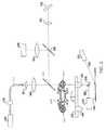
- FIG. 1illustrates an exemplary optical inspection system 10 including a spatial filter mask printer 14 operably connected to, or integrated as part of, an optical inspection tool 12 .
- the optical inspection tool 12may be used to obtain data to define a spatial filter image which is then printed by the printer 14 and used in the optical inspection tool 12 .
- Alternative embodimentsmay include an imaging control computer 16 to supervise and/or control the inspection and printing processes and one or more internal and/or external filter banks 18 for storage of a plurality of previously-printed filters.
- data connections 20are indicated for purposes of illustration only—the various components may be connected to a larger network and may be coordinated and controlled in a variety of ways. For instance, in one embodiment, a universal serial bus (USB) connection is used to link the printer to the imaging tool; particular data connections will vary dependent on the components that are ultimately used.
- USBuniversal serial bus
- the printer 14is integrated with the optical inspection system 12 and/or filter bank 18 via an automated loading apparatus 22 , which is configured to move a printed filter substrate from the printer into the optical inspection tool.
- the filter substratemay be moved between the printer and the optical inspection system by robotic arms 24 and conveyor 26 .
- robotic arms 24 and conveyor 26One skilled in the art will recognize, of course, that other combinations and implementations of loading apparatus are possible using conventional robotics, and the present subject matter is not limited by such particular implementations.
- loading apparatus 22could be reduced or eliminated, and an operator could remove a filter mask and load it into the optical inspection tool.
- use of automated apparatusat least in part is preferred to avoid possible contamination of the filter substrate and/or other equipment.
- loading apparatus 22may also be located within the tool.
- robotic arm 24can grab a printed filter substrate via grab points and pull the substrate out of the exit envelope of the printer. The arm can then rotate and extend to place the substrate into a loading slot of an optical inspection system, with the optical inspection system including a conveyor or other additional internal components to move the inserted filter into the optical path of an object being imaged.
- Conveyor 26may be used to move a filter in or out of filter bank 18 for longer-term storage.
- the printer 14includes appropriate sealing and contaminant control components such that the printer can be used in close proximity to the optical inspection tool rather than outside the cleanroom environment. Such nearby use can save time and increase throughput, since printed filters would not have to be brought in and out of the clean room for use in the optical inspection tool.
- the printermay be located outside the cleanroom, inside the cleanroom, or even be integrated into the optical inspection tool itself without departing from the spirit of the discoveries set forth herein.
- use of the filter bankmay not be necessary depending upon a particular application, and in any event the filters may be stored near the inspection tool and printer or far away.
- the inspection toolitself is adapted to receive and house a plurality of spatial filters.
- FIG. 2illustrates an exemplary optical inspection tool suitable for use in the presently-disclosed system, and similar to embodiments discussed in co-pending U.S. patent application Ser. No. 10/345,097 assigned to Negevtech, Ltd, and incorporated by reference herein in its entirety.
- the inspection toolincludes an object under inspection 100 , in this illustration, a wafer, illumination sources 230 , 300 and 231 , detectors 206 and 502 , and a number of lenses.
- reference numerals 230 , 231 and 300are shown in conjunction with different components, 230 , 231 and 300 can also represent varying the nature of light from a single source by different positioning or use of optical components.
- FIG. 2is an overall schematic side view including the illumination system of a defect detection apparatus.
- three alternative modes of illuminationare provided: Bright Field (BF), Side-illuminated Dark Field (DF) and Orthogonal or Obscured Reflectance Dark Field (ODF).
- BFBright Field
- DFSide-illuminated Dark Field
- ODFOrthogonal or Obscured Reflectance Dark Field
- Each mode of illuminationis used to detect different types of defects in different production process steps. For example in order to detect an embedded defect in a transparent layer, such as silicon oxide, BF illumination is preferred. In order to detect a small particle on a surface, DF illumination may yield better results.
- FIG. 2shows a bright field illuminating laser source 300 delivering its output beam into an optical delivery fiber bundle 160 , preferably by means of a laser to fiber coupler 150 .
- This optical fiber bundle 160serves the dual purposes of providing uniform illumination on the sample and for coherence breaking of the laser illumination.
- the laser beamis imaged by means of illumination transfer lenses 301 , 302 , onto the objective lens in use 201 , which is operative to focus the illumination onto a wafer plane 100 being inspected.
- Appropriate alternative objective lenses 201 ′can be swung into place on an objective revolver 200 , as is known in the microscope arts.
- FIG. 2further includes filter wheel 600 and illustrated mask filters 601 in the illumination path near objective lens 201 ; such mask filters will be discussed in due course. It will be presently recognized that mask filters 601 may be placed and removed from the illumination path as desired—for instance, a filter mask may not be needed in a typical bright field illumination test, and so filter wheel 600 could be rotated such that no filter lay in the illumination path.
- the illumination returned from the waferis collected by the same objective lens 201 , and is deflected from the illumination path by means of a beam splitter 202 , towards a second beam splitter 500 , from where it is reflected through the imaging lens 203 , which images the light from the wafer onto the detector 206 .
- the second beam splitter 500is used to separate the light going to the imaging functionality from the light used in other aspects of the inspection tool, such as the auto-focus detector 502 and related components.
- a dark field side illumination source 231is used to project the required illumination beam 221 onto the wafer 100 .
- an alternative dark field illumination source 230is used to project the required illumination beam 232 via the obscured reflectance mirror 240 onto the wafer 100 orthogonally from above.
- a repetitively pulsed laser sourceis preferably used in the illumination system, although CW laser illumination, other monochromatic, or semi-monochromatic illumination types may also be used.
- CW laser illuminationother monochromatic, or semi-monochromatic illumination types may also be used.
- the third harmonic of a Nd:YAG Laser outputis preferably used.
- other types of repetitively pulsed illuminationmay be used, such as other harmonics, for example the fourth and fifth harmonics of the Nd:YAG Laser.
- Other laserssuch as Excimer Lasers are also suitable.
- the geometry of certain objectsmay consist of a large-scale multiply repetitive pattern that defines the dies of the wafer. Within each die, there are often areas in which there appears an array of a repetitive pattern with a cycle of a few ⁇ m, or a few cycles per micron. This occurs especially in memory chips or in the memory area in a logic chip.
- the arrayWhen coherent or partial coherent illumination is incident on such a periodic array, the array serves as a diffraction grating that reflects the light only in the defined Bragg angles. The reflected light produces a diffraction pattern of spots in the back focal plane of the objective lens.
- the back focal planeis also referred to as the Fourier plane of the lens, since the image obtained in this plane is a two-dimensional Fourier transform of the object.
- Fourier planesmay lie in several different spatial locations depending upon the optics of the particular system being utilized, and so the more general term “Fourier plane” is used below.
- the size of these spotsdepends on the optical quality of the objective lens, but even more on the nature of the incident light.
- An extended source which need be only partially coherent, as used in the dark field side illumination embodiments of certain optical inspection tools,is used to produce defined spots in the Fourier plane.
- the illuminating beamis such an extended light source
- the size and shape of each of the spots in the Fourier planebecomes a miniature image of the extended source.
- each point in the extended sourceit is not necessary that each point in the extended source be a coherent source.
- This extended and partially coherent form of illuminationis successful in generating a Fourier plane diffraction pattern array, because each separate area of the illuminating beam is made up of an assembly of self coherent spots, but unrelated to each other. This outcome may be achieved, for example, via optical treatment performed on the illuminating beam by means of imaging optics at the illumination source.
- the spotsdo not overlap and cover only a relatively small part of the objective pupil. If the structural periodic information from the image can be filtered out, the optical information anomalies resulting from defects on the wafer can be revealed in the form of non-periodic information spread over a wide range of spatial frequencies. This is performed in practice by blocking the transmission of light specifically in the area of those spots, eliminating the information relevant to the repetitive pattern from the image from the remaining optical information transmitted past the Fourier plane, thus making it possible to detect anomalies caused by departures from the desired pattern on the wafer.
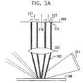
- FIG. 3Aschematically illustrates a method for performing this procedure
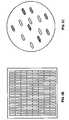
- FIGS. 3B and 3Cdepict an exemplary repetitive pattern and an exemplary Fourier plane image.
- FIGS. 3B and 3Cdepict an exemplary repetitive pattern and an exemplary Fourier plane image.
- an extended source 261which can even be non-parallel, is incident on the wafer 100 under inspection, such as the wafer shown in FIG. 3B .
- the scattered light 262 from the wafer featuresis imaged by the objective lens 201 .
- the back focal plane 209 of this lenswhich is the above-mentioned Fourier plane, there is generated a patterned array of spots 211 representing the repetitive features of the wafer being imaged by the scattered light.
- the array of spotsmay be similar to that shown in FIG. 3C , with the spots featuring differing degrees of brightness, as indicated in FIG. 3C by different cross-hatching.
- a mask 213may be constructed to block the light from the predetermined patterned array of spots 211 and disposed at the Fourier plane. The scattered light 217 from defects present on the wafer die will thus pass the Fourier plane to be imaged and detected by the system without interference from the expected repetitive features of the wafer die.
- FIG. 4illustrates an exemplary method by which this plane can be imaged onto an existing detector by introducing an additional lens into the imaging optics.
- dark field side illumination 221is incident on the wafer 100
- the scattered lightas designated by the dashed lines 280
- the objective 201is collected by the objective 201 , for imaging on the detector 206 by means of the detector imaging lens 203 , all as previously described hereinabove.
- the Fourier plane 209is located behind the objective lens 201 , and may be in a position where it is not easy to locate a detector for direct imaging. Therefore, when the Fourier plane has to be viewed in order to determine the correct Fourier plane filter to construct, an additional imaging lens 282 , known as the Fourier imaging lens, is inserted into the imaging path such that the detector now images the Fourier plane 209 .
- the solid lines 284 in FIG. 4represent the optical imaging path from the Fourier plane to the detector, with the Fourier imaging lens in position. In this manner, the required pattern of the spatial filter in the Fourier plane for a specific die region can be designed according to the imaged field of the object.
- the resulting imagewill be a 2-dimensional Fourier transform of the object image and generally illustrate the frequency components of the imaged object.
- discussion herein of particular optical illumination and inspection tools and techniquesis not intended to limit the Fourier filtering embodiments discussed herein, which may be adapted to multiple types of optical systems.
- the actual layout of the Fourier imagewill depend upon the optical characteristics of the imaged object and inspection tool used to generate the image. Certain object properties will immediately be apparent, however, such as the aforementioned spots due to periodicity of portions of imaged object's structure.
- FIG. 5is a generalized, exemplary illustration of methods for Fourier filtering using a printed filter mask.
- a representation of the object in the Fourier planeis obtained.
- the Fourier plane of an objectmay be imaged using an optical inspection system including a Fourier lens as discussed above as indicated at 502 a in FIG. 5 .
- the Fourier image or characteristics of the objectmay be simulated as shown at 502 b based upon product data such as physical or structural information (such as memory cell size), SEM (scanning electron microscope) or other images, or other data representative of the object's physical characteristics.
- a filter maskcan be defined as shown at 506 a or selected from a pre-existing group, as shown at 506 b .
- a preexisting maskmay be selected either by the user or automatically based on the Fourier characteristics of the object under inspection.
- the preexisting maskmay then be selected from a bank, or a pre-existing mask image printed for use in the tool.
- the systemcan be configured to automatically recognize a previously-inspected type of wafer and select an appropriate filter from a filter bank.
- a usercan observe the Fourier image and define a filter mask by specifying blocking areas based on the Fourier image.
- the blocking areasmay be drawn in a computer program where a drawing area overlays a Fourier image similar to that illustrated in FIG. 3C .
- defining a filter maskcan include simulating the effect of a filter on an object image using software, and may include designing a new filter from scratch or using standardized or previously-saved images or other elements.
- the filter mask imagemay be saved or loaded from memory or other media, such as a hard disk drive, during the design process.
- memory or other mediasuch as a hard disk drive
- a usermanually draws in filter blocking elements to define a filter mask, while in others the filter mask may be defined partially or entirely by computer.
- Other embodimentsfeature a combination of manual and computer definition.
- the defined filter mask imageis sent to a filter mask printer.
- the printermay be networked with or incorporated into an optical inspection tool, and may be configured to operate in accordance with cleanroom requirements.
- an existing maskmay be selected and removed from a filter bank housing a plurality of such masks.
- an existing maskmay be modified.
- an existing mask imageis selected and altered to incorporate additional blocking elements.
- the existing filter mask corresponding to the existing mask imageis then obtained and sent to the printer, which prints the additionally-defined elements on the filter mask.
- an existing mask image that is modifiedcan be printed as an entirely new mask.
- printingcan also include producing or attaching an identification tag or label to the filter mask or associated equipment.
- the optical tool, filter bank(s), and handling apparatusmay be configured to read such tag(s).
- identificationin conjunction with a database program, the filter masks, filter mask images, particular wafers, and particular wafer recipes may all be associated with one another to streamline the inspection process.
- the maskis placed in the Fourier plane of the object being imaged.
- the Fourier planemay lie in a number of different locations, and the mask should be placed accordingly.
- printed masksmay be placed into a filter bank when not in use. Filter banks may be included as part of an inspection tool or apart from the tool, and may be incorporated for use via automated loading apparatus such as robot arms and tracks, manual loading, or a combination of methodologies.
- computer software on imaging computer 16 , the inspection tool 12 , or even another, possibly remote, computer interfaced to network 20can be configured and used to generate a representation of the object's Fourier image and overlay a drawing area thereon.
- a usercan then define blocking areas by drawing shapes, lines, and other markings—for instance, by tracing the brightest areas of the Fourier image and then filling them in.
- the computer softwarecan provide for free hand drawing, predefined shapes, and other graphical manipulations.
- the user-defined areasmay be completely opaque or have varying degrees of opacity depending upon the degree of filtering desired.
- the user-defined areasmay then be stored as a computer file, such as a bitmap image, or in another suitable format.
- the areas through which light will be transmittedmay be defined, with areas to be blocked left blank.
- Reflective Fourier filtersmay be used such that the desired areas of light are reflected into appropriate inspection tool optics; in such a case, the blocking areas specify what parts of the filter should be rendered non-reflecting (or vice-versa).
- the softwaremay include algorithms to convert filter designs applicable to one type of tool into a filter design suitable for another type of tool.
- the computer softwaremay automatically generate, suggest, or define blocking area patterns or portions thereof based upon an analysis of the Fourier image characteristics.
- Analysis softwarecan be configured to select a previously-existing filter mask image based upon such factors as an analysis of the Fourier image, an identification of the object being imaged, or the user-defined areas.
- the pre-existing stored filter mask imagecan be improved or altered by the user, or automatically by the computer.
- the computercan generate simulations of the Fourier image before or after filtering.
- the simulationsmay be of the Fourier image of the object alone based upon an analysis of its physical characteristics input into the computer. For example, in an inspection of a wafer including memory cells, memory cell size or design parameters can be input into simulation software.
- a non-Fourier image(such as an optical or SEM-based image) could be used as the basis for a simulation of a corresponding Fourier image, as well.
- an initial imaging of the Fourier planemay be omitted and the filter constructed based upon the simulated Fourier image from the object properties.
- the simulated Fourier imagecan be used in conjunction with an actual Fourier image during filter definition.
- simulationsmay be used to determine the results if a particular filter mask image design were to be used during imaging.
- the computer simulations and datacan be used to generate feedback for the design process such as suggestions and warnings.
- the image datacan be used to generate a filter mask.
- the filter mask imageis sent to a printer and the image is printed on a filter substrate.
- the substratemay comprise any suitable material, such as plastic, ceramic material, or glass.
- the filtermay be designed for a reflective material, with portions of an image for reflection into a detector and other portions blocked from reflection.
- the filter substratecomprises a 3.0 mm-thick, 48 mm-diameter circular window of fused silica polished to a high optical quality.
- the substratemay have a greater surface area than is ultimately usable, depending upon the system in which it is used.
- the filter surface area and shapepreferably is taken into account in designing filter masks.
- the physical and optical qualities of the filter masks and substratescan be varied by one of ordinary skill in the art in accordance with the particular optics and design of the imaging system in which the filter will be utilized.
- the filter 601may include a substrate 604 disposed in a frame 602 , which may be constructed of any suitable rigid material(s), such as aluminum.
- the frame 602 shown in FIG. 6includes grab points 606 such that the filter can be manipulated without contacting the substrate 604 and the attendant risks of smearing or otherwise introducing physical or optical contamination.
- the filter substratemay be bonded to the frame, or in an alternative embodiment may be removably attached to the frame via one or more latches, clips, or springs such that the filter substrate is secured to the frame for use but may be later separated.
- the filter mask and/or its framecan further comprise one or more identification indicia 608 , such as barcodes, alphanumeric characters, RFID tags, or other suitable identification markings.
- identification indiciasuch as barcodes, alphanumeric characters, RFID tags, or other suitable identification markings.
- the optical inspection tool, filter banks, and/or transport mechanismsmay include appropriate circuitry to read the indicia and identify the filter.
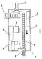
- the mask printer 14comprises an inkjet printer such as the one schematically illustrated in FIG. 7 .
- the inkjet printeris used to apply any suitable ink to a filter substrate.
- UV-curable ink and an inkjet printerare used, but other printing methods and/or other inks may be suitable (or adapted to be suitable) for use in producing printed spatial filters.
- the “printing” aspectshould be understood to broadly refer to any automated rendering and fixation of the filter mask image on a suitable substrate.
- the printerincludes a loading cartridge 700 , a conveyor 702 , at least one inkjet print head 704 , UV curing lamps 706 , and ventilation exhaust connections 708 and other apparatus interfaced to a fab air system.
- UV-curable inkin conjunction with inkjet printing in an appropriately configured printer allows possible contamination risks to be reduced, which may render the printer suitable for integration into an optical inspection tool or suitable for stationing nearby. Additionally, use of UV rather than heat curing reduces the risk of warping or distortion of the filter substrate and related deleterious effects on the optical qualities of the filter. For instance, UV-curable inks are cured by a polymerization that triggered by the UV light, rather than on solvent evaporation. Therefore, the amount of unwanted fumes and outgassing is reduced in such inks, which is an important consideration for fab-compatible processes. Additionally, UV-curable inks have been found to adhere more easily to glass substrates, which reduce wetting problems.
- UV-curable ink and inkjet printingis not intended to be limiting.
- Other appropriately-adapted printing techniquessuch as laser printing, etching, screen printing, and the like can be used on appropriate substrates in a manner that avoids distortion of the image and contaminants to the cleanroom environment.
- heat curing on a substrate sufficiently resistant to warping or in conjunction with a low-temperature-cured inkmay be suitable.
- the printeralso could be configured for use with inks cured by other means, such as microwave or infrared techniques.
- Preferable characteristics in alternative inksinclude cleanliness, long shelf life, little or no outgassing or other contaminants, and the ability to wet the chosen substrate without balling up.
- the UV-curable inkis stored in a cartridge 714 , which may be removable, and can be applied by one or more inkjet heads 704 and then subsequently cured by one or more UV lamps 706 .
- the spatial filter printermay also include a waste/purge tank 710 and appropriate connections to collect and store waste and byproducts of the printing process.
- the printing resolutionis preferably 150 dpi, although other resolutions may be utilized.
- the inkpreferably is selected so that the printed areas will be sufficiently opaque to block desired wavelengths of light, such as those used by optical inspection tool in which the filter will ultimately be utilized.
- black inkis used so that opaque areas have an optical density higher than OD3—that is, the opaque areas preferably allow less than 1/1000 of the light to be transmitted—for 355 nm light.
- Other colorsmay, of course, be suitable for a particular system or application.
- the conveyor 702may move the filter substrate blank from the loading area 700 to the inkjet head or heads, and then on to the UV lamps for curing. The conveyor can then provide the printed substrate to an exit port 712 .
- the exit portis a substantially sealed exit envelope, and all other printer components are housed in a substantially sealed case 716 to prevent escape of contaminants, such as stray ink and other particles.
- the printer casefurther includes ventilation connections 708 configured to interface with conventional clean room exhaust systems so that the printer case may be maintained at a slight underpressure relative to the outside. In this manner, the printer is further suitable for positioning in the clean room proximate an optical inspection tool, or may be integrated as part of the tool itself—the fumes and particles of the printing process are evacuated from the printer, and the completed substrate exits the printer through the exit port ready for use in an inspection tool.
- Filter wheel 600includes a plurality of receptacles for receiving spatial filter masks 601 , and as noted above, may include a “blank” area for use when no mask is needed.
- a particular mask 601can be selected for use and the wheel rotated to place the mask in the Fourier plane of the object under inspection. In this manner, the non-transparent areas of the filter mask will block portions of the object image and the relative intensity of the unfiltered portions, such as those attributable to defects, may stand out more readily at the detector.
- FIG. 8illustrates one exemplary embodiment ( 600 ) of a filter wheel similar to that generally shown in FIG. 2 , but in greater detail and as viewed coaxially with the optical path, rather than from the side as in FIG. 2 .
- Filter wheel 600 as illustratedincludes eight filter stations 610 , although the number of filter stations may be varied. For example, in another embodiment, a 14-station filter turret is used. Stations 610 may be defined by side members 612 , and include a slot, shelf, or other suitable support structure such that various filter assemblies 601 , 601 ′, 601 ′′, 601 ′′′ may be securely supported while in the filter wheel.
- the particular mechanism for securing and supporting the filtersis unimportant so long as the filters are adequately held in place and not misaligned when filter wheel 600 is rotated or when other filters are added or removed from the wheel.
- the filter assembly framesare sized and machined such that the filters fit snugly into stations 610 between side members 612 .
- Filter wheel 600is positioned within an optical inspection tool such that it may be rotated about its axis by appropriate mechanisms, such as a servo motor. The amount of rotation can be selected so that desired stations 610 are moved to align selected filters 601 , 601 ′, and 601 ′′ in the optical path of the inspection tool, shown here as a ray 616 .
- a station 610is preferably kept empty for use in testing operations in which no filter is desired, such as bright-field illumination tests performed using tools such as the one illustrated and discussed in conjunction with FIG. 2 .
- FIG. 8further illustrates loading apparatus 614 , shown here as an end-gripper of a robotic arm.
- An optical inspection tool that includes filter wheel 600may further include appropriate loading mechanisms to provide for automated insertion or removal of filters from the filter bank.
- 614is shown here as a part of a robotic arm, the filter may be loaded into the wheel via a track, conveyor, or other suitable means known to one of skill in the art. Alternatively, an operator can manually load the filter into the filter wheel.
- the loading mechanism 614 or the filter wheel 600may further include barcode, RFID, optical, or other scanners or input devices to read identification indicia associated with each filter in order to identify the filter loaded in stations 610 .
- a filter wheelis but one possible way to place the filter in the Fourier plane.
- an optical inspection toolcould be configured to receive a single spatial filter at a receptacle and move the filter into place via conveyors, tracks, or other apparatus.
- Other embodimentscould utilize both a filter wheel and a conveyor system to relay filters in and out of receptacles on the filter wheel, or could utilize multiple selectable filter wheels.
- the filter wheelis illustrative of but one type of filter bank which may be used in accordance with the present invention. Collections of filters may, of course, be housed in a variety of containers in a variety of configurations, which are generally referred to as filter banks. For instance, another type of filter bank could comprise a stack or cassette of filters. Filter banks may be indexed or otherwise provide for identification of a particular filter or filters stored within the bank; for instance, a filter bank can be configured to identify filters stored therein based upon identification indicia associated with the filter mask and/or frame as discussed above. Filter banks may include components for automated loading, unloading, or other handling of filter substrates. A filter bank may be directly interfaced with an inspection tool or tools, printer(s), or other handling apparatus. Additionally, wheels and other filter banks may be configured to hold other filters beyond those made using a local printer, including even non-printed filters, or other optical components.
- the particular optics of an inspection toolmay result in variously-located Fourier planes beyond the back focal plane of an objective lens. Accordingly, a printed filter mask can be positioned as appropriate within an optical inspection tool to achieve the desired blocking effect.
- a particular inspection toolwas presented for exemplary purposes, the methods and systems disclosed herein may be used with a variety of different optical inspection tools. For instance, although a transparent filter with opaque blocking elements was depicted, the skilled artisan will appreciate the teachings herein are equally applicable to other filtering methodologies, such as a reflectance-based filter wherein desired portions of an image are reflected towards a detector and non-desired portions blocked.
- the optics of a particular toolmay be configured to provide for bright-field testing in conjunction with a Fourier filter.
- a particular object to be imagedmay require more or fewer filters depending upon factors including the size of the object and the field of view of the optical inspection tool.
- Various combinations of filtersmay ultimately be used in an inspection—to provide one example, a group of semiconductor wafers may include wafers of two differing repetitive patterns. Appropriate filter masks may be designed and printed, and then hot-swapped during the inspection process while the optical inspection tool switches between different types of wafer. In the exemplary inspection tool of FIG. 2 , such hot-swapping would be accomplished by rotating the filter wheel 600 .
- the filter masks housed in the filter wheel or other filter banksmay be printed in advance based upon initial sample wafers and stored in filter bank(s) or may be prepared when the wafers are provided to the inspection tool, depending upon the ultimate testing and production circumstances. Additionally, the filter wheel or other banks may be configured to house non-printed filter masks, and other masks and optical components.
Landscapes
- Physics & Mathematics (AREA)
- Engineering & Computer Science (AREA)
- General Physics & Mathematics (AREA)
- General Health & Medical Sciences (AREA)
- Analytical Chemistry (AREA)
- Biochemistry (AREA)
- Chemical & Material Sciences (AREA)
- Life Sciences & Earth Sciences (AREA)
- Immunology (AREA)
- Pathology (AREA)
- Mathematical Physics (AREA)
- Health & Medical Sciences (AREA)
- Multimedia (AREA)
- Theoretical Computer Science (AREA)
- Investigating Materials By The Use Of Optical Means Adapted For Particular Applications (AREA)
Abstract
Description
Claims (21)
Priority Applications (1)
| Application Number | Priority Date | Filing Date | Title |
|---|---|---|---|
| US11/410,276US8031931B2 (en) | 2006-04-24 | 2006-04-24 | Printed fourier filtering in optical inspection tools |
Applications Claiming Priority (1)
| Application Number | Priority Date | Filing Date | Title |
|---|---|---|---|
| US11/410,276US8031931B2 (en) | 2006-04-24 | 2006-04-24 | Printed fourier filtering in optical inspection tools |
Publications (2)
| Publication Number | Publication Date |
|---|---|
| US20070247668A1 US20070247668A1 (en) | 2007-10-25 |
| US8031931B2true US8031931B2 (en) | 2011-10-04 |
Family
ID=38619188
Family Applications (1)
| Application Number | Title | Priority Date | Filing Date |
|---|---|---|---|
| US11/410,276Active2029-04-08US8031931B2 (en) | 2006-04-24 | 2006-04-24 | Printed fourier filtering in optical inspection tools |
Country Status (1)
| Country | Link |
|---|---|
| US (1) | US8031931B2 (en) |
Cited By (2)
| Publication number | Priority date | Publication date | Assignee | Title |
|---|---|---|---|---|
| US9194816B2 (en) | 2013-09-06 | 2015-11-24 | Samsung Electronics Co., Ltd. | Method of detecting a defect of a substrate and apparatus for performing the same |
| US11366307B2 (en) | 2020-08-27 | 2022-06-21 | Kla Corporation | Programmable and reconfigurable mask with MEMS micro-mirror array for defect detection |
Families Citing this family (6)
| Publication number | Priority date | Publication date | Assignee | Title |
|---|---|---|---|---|
| US7869020B1 (en)* | 2007-03-08 | 2011-01-11 | Kla-Tencor Technologies Corp. | Fourier filters, inspection systems, and systems for fabricating fourier filters |
| WO2012016243A2 (en)* | 2010-07-30 | 2012-02-02 | Kla-Tencor Corporation | Region based virtual fourier filter |
| JP5765651B2 (en)* | 2011-02-01 | 2015-08-19 | Jukiオートメーションシステムズ株式会社 | 3D measuring device |
| US9754355B2 (en) | 2015-01-09 | 2017-09-05 | Snap Inc. | Object recognition based photo filters |
| JP6815412B2 (en)* | 2016-03-24 | 2021-01-20 | マツクス−プランク−ゲゼルシヤフト ツール フエルデルング デル ヴイツセンシヤフテン エー フアウMAX−PLANCK−GESELLSCHAFT ZUR FOeRDERUNG DER WISSENSCHAFTEN E.V. | Spatio-temporal photomodulation imaging system, confocal imaging method for objects, and carrier wheel equipment |
| US10116356B2 (en)* | 2016-11-07 | 2018-10-30 | Molecular Devices (Austria) GmbH | System and method for operating a microplate reader |
Citations (201)
| Publication number | Priority date | Publication date | Assignee | Title |
|---|---|---|---|---|
| US3220331A (en)* | 1965-01-27 | 1965-11-30 | Kulicke And Soffa Mfg Company | Contact printing mask alignment apparatus for semiconductor wafer geometry |
| US3598467A (en) | 1969-03-28 | 1971-08-10 | Trw Inc | Er optic diffuser for holography |
| US3790280A (en) | 1972-05-03 | 1974-02-05 | Western Electric Co | Spatial filtering system utilizing compensating elements |
| US4011403A (en) | 1976-03-30 | 1977-03-08 | Northwestern University | Fiber optic laser illuminators |
| US4247203A (en) | 1978-04-03 | 1981-01-27 | Kla Instrument Corporation | Automatic photomask inspection system and apparatus |
| US4323925A (en) | 1980-07-07 | 1982-04-06 | Avco Everett Research Laboratory, Inc. | Method and apparatus for arraying image sensor modules |
| US4347001A (en) | 1978-04-03 | 1982-08-31 | Kla Instruments Corporation | Automatic photomask inspection system and apparatus |
| US4360372A (en) | 1980-11-10 | 1982-11-23 | Northern Telecom Limited | Fiber optic element for reducing speckle noise |
| US4378159A (en) | 1981-03-30 | 1983-03-29 | Tencor Instruments | Scanning contaminant and defect detector |
| US4415240A (en) | 1979-07-27 | 1983-11-15 | Olympus Optical Co., Ltd. | Illumination optical system for an endoscope |
| US4462662A (en) | 1981-06-15 | 1984-07-31 | Xerox Corporation | Imaging system utilizing a gradient index lens array compensated for non-uniform object illumination |
| US4486776A (en) | 1981-06-19 | 1984-12-04 | Hajime Industries Ltd. | Inspection apparatus |
| US4532650A (en) | 1983-05-12 | 1985-07-30 | Kla Instruments Corporation | Photomask inspection apparatus and method using corner comparator defect detection algorithm |
| US4556317A (en) | 1984-02-22 | 1985-12-03 | Kla Instruments Corporation | X-Y Stage for a patterned wafer automatic inspection system |
| US4579455A (en) | 1983-05-09 | 1986-04-01 | Kla Instruments Corporation | Photomask inspection apparatus and method with improved defect detection |
| US4588293A (en) | 1983-12-12 | 1986-05-13 | The Perkin-Elmer Corporation | Method and apparatus for inspecting photomasks to detect defects |
| US4589736A (en) | 1984-11-23 | 1986-05-20 | Xerox Corporation | Two row reduction/enlargement gradient index lens array having square-ended fibers |
| US4597665A (en) | 1983-12-09 | 1986-07-01 | Tencor Instruments | Dual collector optical flaw detector |
| US4618938A (en) | 1984-02-22 | 1986-10-21 | Kla Instruments Corporation | Method and apparatus for automatic wafer inspection |
| US4619508A (en) | 1984-04-28 | 1986-10-28 | Nippon Kogaku K. K. | Illumination optical arrangement |
| US4639587A (en) | 1984-02-22 | 1987-01-27 | Kla Instruments Corporation | Automatic focusing system for a microscope |
| US4644172A (en) | 1984-02-22 | 1987-02-17 | Kla Instruments Corporation | Electronic control of an automatic wafer inspection system |
| US4725722A (en) | 1985-04-12 | 1988-02-16 | Hitachi, Ltd. | Automatic focusing method and apparatus utilizing contrasts of projected pattern |
| US4734923A (en) | 1986-05-19 | 1988-03-29 | Hampshire Instruments, Inc | Lithographic system mask inspection device |
| US4760265A (en) | 1986-01-18 | 1988-07-26 | Kabushiki Kaisha Toyoda Jidoshokki Seisakusho | Method and device for detecting defects of patterns in microelectronic devices |
| US4763975A (en) | 1987-04-28 | 1988-08-16 | Spectra Diode Laboratories, Inc. | Optical system with bright light output |
| US4766324A (en) | 1987-08-07 | 1988-08-23 | Tencor Instruments | Particle detection method including comparison between sequential scans |
| US4805123A (en) | 1986-07-14 | 1989-02-14 | Kla Instruments Corporation | Automatic photomask and reticle inspection method and apparatus including improved defect detector and alignment sub-systems |
| US4806774A (en) | 1987-06-08 | 1989-02-21 | Insystems, Inc. | Inspection system for array of microcircuit dies having redundant circuit patterns |
| US4845558A (en) | 1987-12-03 | 1989-07-04 | Kla Instruments Corporation | Method and apparatus for detecting defects in repeated microminiature patterns |
| US4877326A (en) | 1988-02-19 | 1989-10-31 | Kla Instruments Corporation | Method and apparatus for optical inspection of substrates |
| US4898471A (en) | 1987-06-18 | 1990-02-06 | Tencor Instruments | Particle detection on patterned wafers and the like |
| US4929081A (en) | 1987-02-27 | 1990-05-29 | Mitsubishi Denki Kabushiki Kaisha | System for detecting defects in a regularly arranged pattern such as an integrated circuit or the like |
| US4964692A (en) | 1982-07-21 | 1990-10-23 | Smith & Nephew Dyonics, Inc. | Fiber bundle illumination system |
| US4967095A (en) | 1989-06-28 | 1990-10-30 | Tencor Instruments | Method and apparatus for detecting and sizing particles on surfaces |
| US4969198A (en) | 1986-04-17 | 1990-11-06 | International Business Machines Corporation | System for automatic inspection of periodic patterns |
| US5008743A (en) | 1988-03-24 | 1991-04-16 | Orbot Systems Ltd. | Telecentric imaging system optical inspection machine using the same and method for correcting optical distortion produced thereby |
| US5012081A (en) | 1989-06-22 | 1991-04-30 | Northrop Corporation | Strapdown stellar sensor and holographic lens therefor |
| US5029975A (en) | 1990-01-24 | 1991-07-09 | The Mitre Corporation | Despeckling screen utilizing optical fibers and method of reducing interference using same |
| US5038048A (en) | 1988-12-23 | 1991-08-06 | Hitachi, Ltd. | Defect detection system and method for pattern to be inspected utilizing multiple-focus image signals |
| US5046847A (en) | 1987-10-30 | 1991-09-10 | Hitachi Ltd. | Method for detecting foreign matter and device for realizing same |
| US5056765A (en) | 1989-06-06 | 1991-10-15 | Orbot Systems, Ltd. | Immobilizing device particularly useful during processing or testing flat workpieces |
| US5058982A (en) | 1989-06-21 | 1991-10-22 | Orbot Systems Ltd. | Illumination system and inspection apparatus including same |
| US5076692A (en) | 1990-05-31 | 1991-12-31 | Tencor Instruments | Particle detection on a patterned or bare wafer surface |
| US5112129A (en) | 1990-03-02 | 1992-05-12 | Kla Instruments Corporation | Method of image enhancement for the coherence probe microscope with applications to integrated circuit metrology |
| US5153668A (en) | 1990-05-11 | 1992-10-06 | Orbot Systems Ltd. | Optical inspection apparatus and illumination system particularly useful therein |
| US5172000A (en) | 1990-11-02 | 1992-12-15 | Insystems, Inc. | Spatial filter for optically based defect inspection system |
| US5177559A (en) | 1991-05-17 | 1993-01-05 | International Business Machines Corporation | Dark field imaging defect inspection system for repetitive pattern integrated circuits |
| US5185812A (en) | 1990-02-14 | 1993-02-09 | Kabushiki Kaisha Toshiba | Optical pattern inspection system |
| US5194959A (en) | 1989-12-21 | 1993-03-16 | Ricoh Company, Ltd. and Nippon Telegraph and Telephone Corporation | Image forming apparatus for forming image corresponding to subject, by dividing optical image corresponding to the subject into plural adjacent optical image parts |
| JPH05190421A (en) | 1992-01-17 | 1993-07-30 | Canon Inc | Substrate alignment method |
| US5233460A (en) | 1992-01-31 | 1993-08-03 | Regents Of The University Of California | Method and means for reducing speckle in coherent laser pulses |
| US5264912A (en) | 1992-02-07 | 1993-11-23 | Tencor Instruments | Speckle reduction track filter apparatus for optical inspection of patterned substrates |
| US5267017A (en) | 1992-05-20 | 1993-11-30 | Applied Materials, Inc. | Method of particle analysis on a mirror wafer |
| US5276498A (en) | 1992-05-12 | 1994-01-04 | Tencor Instruments | Adaptive spatial filter for surface inspection |
| US5302999A (en) | 1992-02-04 | 1994-04-12 | Hitachi, Ltd. | Illumination method, illumination apparatus and projection exposure apparatus |
| US5381004A (en) | 1993-08-31 | 1995-01-10 | Applied Materials, Inc. | Particle analysis of notched wafers |
| US5386228A (en) | 1991-06-20 | 1995-01-31 | Canon Kabushiki Kaisha | Image pickup device including means for adjusting sensitivity of image pickup elements |
| US5422724A (en) | 1992-05-20 | 1995-06-06 | Applied Materials, Inc. | Multiple-scan method for wafer particle analysis |
| US5432331A (en) | 1994-06-07 | 1995-07-11 | Eastman Kodak Company | Method and apparatus for detecting focus of moving images with tilted plane detector and time delay means |
| US5461237A (en) | 1993-03-26 | 1995-10-24 | Nikon Corporation | Surface-position setting apparatus |
| US5469274A (en) | 1992-03-12 | 1995-11-21 | Sharp Kabushiki Kaisha | Image processing apparatus for combining differently corrected images |
| US5471341A (en) | 1991-07-17 | 1995-11-28 | Optron Systems, Inc. | Membrane light modulating systems |
| US5471066A (en) | 1993-08-26 | 1995-11-28 | Nikon Corporation | Defect inspection apparatus of rotary type |
| US5506676A (en) | 1994-10-25 | 1996-04-09 | Pixel Systems, Inc. | Defect detection using fourier optics and a spatial separator for simultaneous optical computing of separated fourier transform components |
| JPH08154210A (en) | 1994-11-28 | 1996-06-11 | Kubota Corp | Imaging device |
| US5537669A (en) | 1993-09-30 | 1996-07-16 | Kla Instruments Corporation | Inspection method and apparatus for the inspection of either random or repeating patterns |
| JPH08292361A (en) | 1995-04-24 | 1996-11-05 | Olympus Optical Co Ltd | Prism fixing device |
| US5583632A (en) | 1994-06-21 | 1996-12-10 | New Creation Co., Ltd. | Apparatus for two or three dimensional optical inspection of a sample |
| US5586058A (en) | 1990-12-04 | 1996-12-17 | Orbot Instruments Ltd. | Apparatus and method for inspection of a patterned object by comparison thereof to a reference |
| US5589862A (en)* | 1992-07-31 | 1996-12-31 | Canon Kabushiki Kaisha | Liquid storing container for recording apparatus |
| US5604585A (en) | 1995-03-31 | 1997-02-18 | Tencor Instruments | Particle detection system employing a subsystem for collecting scattered light from the particles |
| US5608155A (en) | 1993-04-30 | 1997-03-04 | Applied Materials, Inc. | Method and apparatus for detecting particles on a substrate |
| US5617203A (en) | 1993-10-01 | 1997-04-01 | Hamamatsu Photonics K.K. | Optical detector employing an optically-addressed spatial light modulator |
| US5619429A (en) | 1990-12-04 | 1997-04-08 | Orbot Instruments Ltd. | Apparatus and method for inspection of a patterned object by comparison thereof to a reference |
| US5619588A (en) | 1992-07-27 | 1997-04-08 | Orbot Instruments Ltd. | Apparatus and method for comparing and aligning two digital representations of an image |
| US5629768A (en) | 1993-01-28 | 1997-05-13 | Nikon Corporation | Defect inspecting apparatus |
| EP0557558B1 (en) | 1992-02-26 | 1997-06-18 | Mitsui Mining & Smelting Co., Ltd. | Apparatus for inspecting the surface of materials |
| US5659172A (en) | 1995-06-21 | 1997-08-19 | Opal Technologies Ltd. | Reliable defect detection using multiple perspective scanning electron microscope images |
| US5659390A (en) | 1995-02-09 | 1997-08-19 | Inspex, Inc. | Method and apparatus for detecting particles on a surface of a semiconductor wafer having repetitive patterns |
| US5661575A (en) | 1990-10-09 | 1997-08-26 | Matsushita Electric Industrial Co., Ltd. | Gradation correction method and device |
| US5689592A (en) | 1993-12-22 | 1997-11-18 | Vivo Software, Inc. | Parallel processing of digital signals in a single arithmetic/logic unit |
| US5694481A (en) | 1995-04-12 | 1997-12-02 | Semiconductor Insights Inc. | Automated design analysis system for generating circuit schematics from high magnification images of an integrated circuit |
| US5699447A (en) | 1990-11-16 | 1997-12-16 | Orbot Instruments Ltd. | Two-phase optical inspection method and apparatus for defect detection |
| US5784189A (en) | 1991-03-06 | 1998-07-21 | Massachusetts Institute Of Technology | Spatial light modulator |
| US5798829A (en) | 1996-03-05 | 1998-08-25 | Kla-Tencor Corporation | Single laser bright field and dark field system for detecting anomalies of a sample |
| US5797317A (en) | 1996-09-06 | 1998-08-25 | Orbot Instruments Ltd. | Universal chuck for holding plates of various sizes |
| US5822055A (en) | 1995-06-06 | 1998-10-13 | Kla Instruments Corporation | Optical inspection of a specimen using multi-channel responses from the specimen using bright and darkfield detection |
| US5825482A (en) | 1995-09-29 | 1998-10-20 | Kla-Tencor Corporation | Surface inspection system with misregistration error correction and adaptive illumination |
| US5835225A (en) | 1994-11-30 | 1998-11-10 | Micron Technology, Inc. | Surface properties detection by reflectance metrology |
| US5835278A (en) | 1990-11-06 | 1998-11-10 | Rubin; Leoind Borisovich | Optical system for partitioning a real image |
| US5859698A (en) | 1997-05-07 | 1999-01-12 | Nikon Corporation | Method and apparatus for macro defect detection using scattered light |
| JPH1114357A (en) | 1997-06-20 | 1999-01-22 | Technical Syst:Kk | Automatic tracking device of surveying equipment |
| US5864394A (en) | 1994-06-20 | 1999-01-26 | Kla-Tencor Corporation | Surface inspection system |
| US5872862A (en) | 1991-10-04 | 1999-02-16 | Fujitsu Limited | Electron beam tester |
| US5883710A (en) | 1994-12-08 | 1999-03-16 | Kla-Tencor Corporation | Scanning system for inspecting anomalies on surfaces |
| US5892579A (en) | 1996-07-16 | 1999-04-06 | Orbot Instruments Ltd. | Optical inspection method and apparatus |
| US5909276A (en) | 1997-03-31 | 1999-06-01 | Microtherm, Llc | Optical inspection module and method for detecting particles and defects on substrates in integrated process tools |
| US5912735A (en) | 1997-07-29 | 1999-06-15 | Kla-Tencor Corporation | Laser/white light viewing laser imaging system |
| US5917588A (en) | 1996-11-04 | 1999-06-29 | Kla-Tencor Corporation | Automated specimen inspection system for and method of distinguishing features or anomalies under either bright field or dark field illumination |
| US5939647A (en) | 1996-01-16 | 1999-08-17 | Applied Materials, Inc. | Surface particle sampling head having a rotatable probe |
| US5970168A (en) | 1997-08-05 | 1999-10-19 | Kla-Tencor Corporation | Fourier filtering mechanism for inspecting wafers |
| US5991699A (en) | 1995-05-04 | 1999-11-23 | Kla Instruments Corporation | Detecting groups of defects in semiconductor feature space |
| EP0959378A1 (en) | 1998-05-20 | 1999-11-24 | Sony Corporation | Optical coherence reduction method and device, illuminating method and system |
| US5995665A (en) | 1995-05-31 | 1999-11-30 | Canon Kabushiki Kaisha | Image processing apparatus and method |
| US6008786A (en) | 1996-05-22 | 1999-12-28 | International Business Machines Corporation | Method for driving halftone display for a liquid crystal display |
| US6020957A (en)* | 1998-04-30 | 2000-02-01 | Kla-Tencor Corporation | System and method for inspecting semiconductor wafers |
| US6023056A (en) | 1998-05-04 | 2000-02-08 | Eastman Kodak Company | Scene-based autofocus method |
| US6064517A (en) | 1996-07-22 | 2000-05-16 | Kla-Tencor Corporation | High NA system for multiple mode imaging |
| US6075375A (en) | 1997-06-11 | 2000-06-13 | Applied Materials, Inc. | Apparatus for wafer detection |
| US6081381A (en) | 1998-10-26 | 2000-06-27 | Polametrics, Inc. | Apparatus and method for reducing spatial coherence and for improving uniformity of a light beam emitted from a coherent light source |
| US6081325A (en) | 1996-06-04 | 2000-06-27 | Kla-Tencor Corporation | Optical scanning system for surface inspection |
| US6099596A (en) | 1997-07-23 | 2000-08-08 | Applied Materials, Inc. | Wafer out-of-pocket detection tool |
| US6122046A (en) | 1998-10-02 | 2000-09-19 | Applied Materials, Inc. | Dual resolution combined laser spot scanning and area imaging inspection |
| US6124924A (en) | 1998-12-24 | 2000-09-26 | Applied Materials, Inc. | Focus error correction method and apparatus |
| US6134365A (en) | 1998-06-01 | 2000-10-17 | Colvin; James Barry | Coherent illumination system and method |
| US6133981A (en)* | 1997-06-11 | 2000-10-17 | Tokyo Electron Ltd. | Processing system |
| US6147664A (en) | 1997-08-29 | 2000-11-14 | Candescent Technologies Corporation | Controlling the brightness of an FED device using PWM on the row side and AM on the column side |
| US6169282B1 (en) | 1997-10-29 | 2001-01-02 | Hitachi, Ltd. | Defect inspection method and apparatus therefor |
| US6172349B1 (en) | 1997-03-31 | 2001-01-09 | Kla-Tencor Corporation | Autofocusing apparatus and method for high resolution microscope system |
| US6170973B1 (en) | 1997-11-26 | 2001-01-09 | Cognex Corporation | Method and apparatus for wide-angle illumination in line-scanning machine vision devices |
| US6175646B1 (en) | 1997-09-04 | 2001-01-16 | Texas Instruments Incorporated | Apparatus for detecting defective integrated circuit dies in wafer form |
| US6175645B1 (en) | 1998-01-22 | 2001-01-16 | Applied Materials, Inc. | Optical inspection method and apparatus |
| US6201601B1 (en) | 1997-09-19 | 2001-03-13 | Kla-Tencor Corporation | Sample inspection system |
| US6208750B1 (en) | 1998-07-07 | 2001-03-27 | Applied Materials, Inc. | Method for detecting particles using illumination with several wavelengths |
| US6208411B1 (en) | 1998-09-28 | 2001-03-27 | Kla-Tencor Corporation | Massively parallel inspection and imaging system |
| US6226116B1 (en) | 1999-11-30 | 2001-05-01 | Eastman Kodak Company | Magnetic micro-shutters |
| US6236454B1 (en) | 1997-12-15 | 2001-05-22 | Applied Materials, Inc. | Multiple beam scanner for an inspection system |
| US6246822B1 (en) | 1999-05-18 | 2001-06-12 | The Boeing Company | Fiber-coupled receiver and associated method |
| US6249630B1 (en) | 1996-12-13 | 2001-06-19 | Imra America, Inc. | Apparatus and method for delivery of dispersion-compensated ultrashort optical pulses with high peak power |
| US6250778B1 (en) | 1998-12-29 | 2001-06-26 | Sony Corporation | Lighting system, and image display apparatus |
| US6256093B1 (en) | 1998-06-25 | 2001-07-03 | Applied Materials, Inc. | On-the-fly automatic defect classification for substrates using signal attributes |
| US6268916B1 (en) | 1999-05-11 | 2001-07-31 | Kla-Tencor Corporation | System for non-destructive measurement of samples |
| US6268093B1 (en) | 1999-10-13 | 2001-07-31 | Applied Materials, Inc. | Method for reticle inspection using aerial imaging |
| US6267005B1 (en) | 1994-12-22 | 2001-07-31 | Kla-Tencor Corporation | Dual stage instrument for scanning a specimen |
| US6271916B1 (en) | 1994-03-24 | 2001-08-07 | Kla-Tencor Corporation | Process and assembly for non-destructive surface inspections |
| US6282309B1 (en) | 1998-05-29 | 2001-08-28 | Kla-Tencor Corporation | Enhanced sensitivity automated photomask inspection system |
| US6285400B1 (en) | 1996-09-26 | 2001-09-04 | Nec Corporation | Solid state image pick-up device equipped with charge coupled device having incident surface alignable with focal plane |
| US6288780B1 (en) | 1995-06-06 | 2001-09-11 | Kla-Tencor Technologies Corp. | High throughput brightfield/darkfield wafer inspection system using advanced optical techniques |
| US6292228B1 (en) | 1998-06-29 | 2001-09-18 | Lg Electronics Inc. | Device and method for auto-adjustment of image condition in display using data representing both brightness or contrast and color temperature |
| US20010033386A1 (en) | 2000-01-07 | 2001-10-25 | Kranz David M | Phase profilometry system with telecentric projector |
| US6317514B1 (en) | 1998-09-09 | 2001-11-13 | Applied Materials, Inc. | Method and apparatus for inspection of patterned semiconductor wafers |
| US6324298B1 (en) | 1998-07-15 | 2001-11-27 | August Technology Corp. | Automated wafer defect inspection system and a process of performing such inspection |
| US6347173B1 (en) | 1998-05-15 | 2002-02-12 | Sony Corporation | Optical coherence reduction method and its device, illuminating method and its system and optical fiber bundle |
| US6361910B1 (en) | 2000-02-03 | 2002-03-26 | Applied Materials, Inc | Straight line defect detection |
| US20020037099A1 (en) | 2000-09-28 | 2002-03-28 | Riki Ogawa | Pattern inspection apparatus and pattern inspection method |
| US6366315B1 (en) | 1993-06-15 | 2002-04-02 | Deutsches Zentrum für Luft- und Raumfahrt e.V. | Arrangement for lengthening sensor lines in an optoelectronic camera |
| US6369888B1 (en) | 1999-11-17 | 2002-04-09 | Applied Materials, Inc. | Method and apparatus for article inspection including speckle reduction |
| US20020054291A1 (en) | 1997-06-27 | 2002-05-09 | Tsai Bin-Ming Benjamin | Inspection system simultaneously utilizing monochromatic darkfield and broadband brightfield illumination sources |
| US6392747B1 (en) | 1999-06-11 | 2002-05-21 | Raytheon Company | Method and device for identifying an object and determining its location |
| US6456769B1 (en) | 1999-09-02 | 2002-09-24 | Asahi Kogaku Kogyo Kabushiki Kaisha | Fiber bundle and endoscope apparatus |
| US6456420B1 (en) | 2000-07-27 | 2002-09-24 | Mcnc | Microelectromechanical elevating structures |
| US20020171028A1 (en) | 2001-05-15 | 2002-11-21 | Haim Feldman | Focus error correction method and apparatus |
| US20020191066A1 (en)* | 2001-05-30 | 2002-12-19 | Alain Bouchard | High speed photo-printing apparatus |
| US6504948B1 (en) | 1997-09-04 | 2003-01-07 | Texas Instruments Incorporated | Apparatus and method for automatically detecting defects on silicon dies on silicon wafers |
| US20030048957A1 (en) | 2001-09-07 | 2003-03-13 | Nline Corporation | System and method for correlated noise removal in complex imaging systems |
| US6536882B1 (en)* | 2000-07-26 | 2003-03-25 | Eastman Kodak Company | Inkjet printhead having substrate feedthroughs for accommodating conductors |
| US6563653B2 (en) | 1996-08-16 | 2003-05-13 | Imaging Research, Inc. | Digital imaging system for assays in well plates, gels and blots |
| US6618093B1 (en) | 1998-01-15 | 2003-09-09 | Chauncey F. Levy | Distortion-free imaging device having curved photosensor |
| US6628681B2 (en) | 2001-03-16 | 2003-09-30 | Sony Corporation | Laser apparatus |
| US6627865B1 (en) | 2001-05-15 | 2003-09-30 | Raytheon Company | Nonplanar integrated optical device array structure and a method for its fabrication |
| US20030184739A1 (en) | 2002-03-28 | 2003-10-02 | Kla-Tencor Technologies Corporation | UV compatible programmable spatial filter |
| US6630996B2 (en) | 2000-11-15 | 2003-10-07 | Real Time Metrology, Inc. | Optical method and apparatus for inspecting large area planar objects |
| US6633375B1 (en) | 1999-01-29 | 2003-10-14 | Leica Microsystems Semiconductor Gmbh | Method and device for optically examining structured surfaces of objects |
| US20030202178A1 (en) | 2001-09-19 | 2003-10-30 | Olympus Optical Co., Ltd. | Semiconductor wafer inspection apparatus |
| US20030210391A1 (en) | 2002-05-10 | 2003-11-13 | Sachio Uto | Method and apparatus for inspecting pattern defects |
| US6657714B2 (en) | 2001-09-24 | 2003-12-02 | Applied Materials, Inc. | Defect detection with enhanced dynamic range |
| US6657157B1 (en)* | 2000-06-07 | 2003-12-02 | Westar Photonics, Inc. | Method, system and product for producing a reflective mask mirror and for ablating an object using said reflective mask mirror |
| US20030227618A1 (en) | 2002-05-06 | 2003-12-11 | Applied Materials Israel Ltd | High speed laser scanning inspection system |
| US20030227617A1 (en) | 2002-06-07 | 2003-12-11 | Minoru Yoshida | Method and apparatus for detecting pattern defects |
| US6686995B2 (en) | 2002-03-28 | 2004-02-03 | Kla-Tencor Technologies Corporation | Two-dimensional UV compatible programmable spatial filter |
| US6686602B2 (en) | 2002-01-15 | 2004-02-03 | Applied Materials, Inc. | Patterned wafer inspection using spatial filtering |
| US6693664B2 (en) | 1999-06-30 | 2004-02-17 | Negevtech | Method and system for fast on-line electro-optical detection of wafer defects |
| US20040032581A1 (en) | 2002-01-15 | 2004-02-19 | Mehrdad Nikoonahad | Systems and methods for inspection of specimen surfaces |
| US6707544B1 (en) | 1999-09-07 | 2004-03-16 | Applied Materials, Inc. | Particle detection and embedded vision system to enhance substrate yield and throughput |
| US6710868B2 (en) | 2002-05-22 | 2004-03-23 | Applied Materials, Inc. | Optical inspection system with dual detection heads |
| US20040057611A1 (en) | 2002-09-23 | 2004-03-25 | Byoung-Ho Lee | Method for selecting reference images, method and apparatus for inspecting patterns on wafers, and method for dividing a wafer into application regions |
| US20040066507A1 (en) | 2002-10-02 | 2004-04-08 | Kla-Tencor Technologies Corporation | Process for identifying defects in a substrate having non-uniform surface properties |
| US6724473B2 (en) | 2002-03-27 | 2004-04-20 | Kla-Tencor Technologies Corporation | Method and system using exposure control to inspect a surface |
| US20040105093A1 (en)* | 2002-11-29 | 2004-06-03 | Akira Hamamatsu | Inspection method and inspection apparatus |
| US20040136665A1 (en) | 2003-01-15 | 2004-07-15 | Negevtech Ltd. | Fiber optical illumination system |
| US20040146295A1 (en) | 2003-01-15 | 2004-07-29 | Negevtech Ltd. | System for detection of wafer defects |
| US6774991B1 (en) | 1999-05-27 | 2004-08-10 | Inspex Incorporated | Method and apparatus for inspecting a patterned semiconductor wafer |
| US6791072B1 (en) | 2002-05-22 | 2004-09-14 | National Semiconductor Corporation | Method and apparatus for forming curved image sensor module |
| US6796699B2 (en) | 2000-06-17 | 2004-09-28 | Leica Microsystems Heidelberg Gmbh | Laser illuminator and method |
| US6818459B2 (en) | 2000-09-20 | 2004-11-16 | Kla-Tencor Technologies Corp. | Methods and systems for determining a presence of macro defects and overlay of a specimen |
| WO2005022969A2 (en)* | 2003-09-02 | 2005-03-10 | Pixdro Ltd. | Method and system for creating fine lines using ink jet technology |
| US20050084766A1 (en) | 2001-12-14 | 2005-04-21 | Micronic Laser Systems Ab | Method and apparatus for patterning a workpiece |
| US6895149B1 (en) | 2002-05-13 | 2005-05-17 | James Jeffery Jacob | Apparatus for beam homogenization and speckle reduction |
| US20050114823A1 (en)* | 2003-11-26 | 2005-05-26 | Bernd Kuchler | Method for improving a simulation model of photolithographic projection |
| US6919958B2 (en) | 1999-02-01 | 2005-07-19 | Therma-Wave, Inc. | Wafer metrology apparatus and method |
| US6941007B1 (en) | 2000-01-28 | 2005-09-06 | Micron Technology, Inc. | Pattern recognition with the use of multiple images |
| US20050195389A1 (en) | 2004-03-05 | 2005-09-08 | Orbotech Ltd | System and method for inspecting electrical circuits utilizing reflective and fluorescent imagery |
| US6947587B1 (en) | 1998-04-21 | 2005-09-20 | Hitachi, Ltd. | Defect inspection method and apparatus |
| US6985184B2 (en) | 2001-03-29 | 2006-01-10 | Fujinon Corporation | Electronic camera |
| US20060007434A1 (en) | 2004-07-12 | 2006-01-12 | Dov Furman | Multi mode inspection method and apparatus |
| US20060012781A1 (en) | 2004-07-14 | 2006-01-19 | Negevtech Ltd. | Programmable spatial filter for wafer inspection |
| US20060193506A1 (en) | 2005-02-28 | 2006-08-31 | Negevtech Ltd. | Method and apparatus for detecting defects in wafers including alignment of the wafer images so as to induce the same smear in all images |
| US20060193507A1 (en) | 2005-02-28 | 2006-08-31 | Negevtech Ltd. | Method and apparatus for detecting defects in wafers |
| US7265900B2 (en) | 2002-09-30 | 2007-09-04 | Applied Materials, Inc. | Inspection system with oblique viewing angle |
| US7630069B2 (en) | 2002-09-30 | 2009-12-08 | Applied Materials, Inc. | Illumination system for optical inspection |
Family Cites Families (1)
| Publication number | Priority date | Publication date | Assignee | Title |
|---|---|---|---|---|
| US7339033B2 (en)* | 1998-06-26 | 2008-03-04 | Genentech, Inc. | Pro1481 |
- 2006
- 2006-04-24USUS11/410,276patent/US8031931B2/enactiveActive
Patent Citations (226)
| Publication number | Priority date | Publication date | Assignee | Title |
|---|---|---|---|---|
| US3220331A (en)* | 1965-01-27 | 1965-11-30 | Kulicke And Soffa Mfg Company | Contact printing mask alignment apparatus for semiconductor wafer geometry |
| US3598467A (en) | 1969-03-28 | 1971-08-10 | Trw Inc | Er optic diffuser for holography |
| US3790280A (en) | 1972-05-03 | 1974-02-05 | Western Electric Co | Spatial filtering system utilizing compensating elements |
| US4011403A (en) | 1976-03-30 | 1977-03-08 | Northwestern University | Fiber optic laser illuminators |
| US4247203A (en) | 1978-04-03 | 1981-01-27 | Kla Instrument Corporation | Automatic photomask inspection system and apparatus |
| US4347001A (en) | 1978-04-03 | 1982-08-31 | Kla Instruments Corporation | Automatic photomask inspection system and apparatus |
| US4610513A (en) | 1979-07-27 | 1986-09-09 | Olympus Optical Co., Ltd. | Illumination optical system for an endoscope |
| US4415240A (en) | 1979-07-27 | 1983-11-15 | Olympus Optical Co., Ltd. | Illumination optical system for an endoscope |
| US4323925A (en) | 1980-07-07 | 1982-04-06 | Avco Everett Research Laboratory, Inc. | Method and apparatus for arraying image sensor modules |
| US4360372A (en) | 1980-11-10 | 1982-11-23 | Northern Telecom Limited | Fiber optic element for reducing speckle noise |
| US4378159A (en) | 1981-03-30 | 1983-03-29 | Tencor Instruments | Scanning contaminant and defect detector |
| US4462662A (en) | 1981-06-15 | 1984-07-31 | Xerox Corporation | Imaging system utilizing a gradient index lens array compensated for non-uniform object illumination |
| US4486776A (en) | 1981-06-19 | 1984-12-04 | Hajime Industries Ltd. | Inspection apparatus |
| US4964692A (en) | 1982-07-21 | 1990-10-23 | Smith & Nephew Dyonics, Inc. | Fiber bundle illumination system |
| US4579455A (en) | 1983-05-09 | 1986-04-01 | Kla Instruments Corporation | Photomask inspection apparatus and method with improved defect detection |
| US4532650A (en) | 1983-05-12 | 1985-07-30 | Kla Instruments Corporation | Photomask inspection apparatus and method using corner comparator defect detection algorithm |
| US4597665A (en) | 1983-12-09 | 1986-07-01 | Tencor Instruments | Dual collector optical flaw detector |
| US4601576A (en) | 1983-12-09 | 1986-07-22 | Tencor Instruments | Light collector for optical contaminant and flaw detector |
| US4588293A (en) | 1983-12-12 | 1986-05-13 | The Perkin-Elmer Corporation | Method and apparatus for inspecting photomasks to detect defects |
| US4618938A (en) | 1984-02-22 | 1986-10-21 | Kla Instruments Corporation | Method and apparatus for automatic wafer inspection |
| US4639587A (en) | 1984-02-22 | 1987-01-27 | Kla Instruments Corporation | Automatic focusing system for a microscope |
| US4644172A (en) | 1984-02-22 | 1987-02-17 | Kla Instruments Corporation | Electronic control of an automatic wafer inspection system |
| US4556317A (en) | 1984-02-22 | 1985-12-03 | Kla Instruments Corporation | X-Y Stage for a patterned wafer automatic inspection system |
| US4619508A (en) | 1984-04-28 | 1986-10-28 | Nippon Kogaku K. K. | Illumination optical arrangement |
| US4589736A (en) | 1984-11-23 | 1986-05-20 | Xerox Corporation | Two row reduction/enlargement gradient index lens array having square-ended fibers |
| US4725722A (en) | 1985-04-12 | 1988-02-16 | Hitachi, Ltd. | Automatic focusing method and apparatus utilizing contrasts of projected pattern |
| US4760265A (en) | 1986-01-18 | 1988-07-26 | Kabushiki Kaisha Toyoda Jidoshokki Seisakusho | Method and device for detecting defects of patterns in microelectronic devices |
| US4969198A (en) | 1986-04-17 | 1990-11-06 | International Business Machines Corporation | System for automatic inspection of periodic patterns |
| US4734923A (en) | 1986-05-19 | 1988-03-29 | Hampshire Instruments, Inc | Lithographic system mask inspection device |
| US4805123A (en) | 1986-07-14 | 1989-02-14 | Kla Instruments Corporation | Automatic photomask and reticle inspection method and apparatus including improved defect detector and alignment sub-systems |
| US4805123B1 (en) | 1986-07-14 | 1998-10-13 | Kla Instr Corp | Automatic photomask and reticle inspection method and apparatus including improved defect detector and alignment sub-systems |
| US4929081A (en) | 1987-02-27 | 1990-05-29 | Mitsubishi Denki Kabushiki Kaisha | System for detecting defects in a regularly arranged pattern such as an integrated circuit or the like |
| US4763975A (en) | 1987-04-28 | 1988-08-16 | Spectra Diode Laboratories, Inc. | Optical system with bright light output |
| US4806774A (en) | 1987-06-08 | 1989-02-21 | Insystems, Inc. | Inspection system for array of microcircuit dies having redundant circuit patterns |
| US4898471A (en) | 1987-06-18 | 1990-02-06 | Tencor Instruments | Particle detection on patterned wafers and the like |
| US4766324A (en) | 1987-08-07 | 1988-08-23 | Tencor Instruments | Particle detection method including comparison between sequential scans |
| US5046847A (en) | 1987-10-30 | 1991-09-10 | Hitachi Ltd. | Method for detecting foreign matter and device for realizing same |
| US4845558A (en) | 1987-12-03 | 1989-07-04 | Kla Instruments Corporation | Method and apparatus for detecting defects in repeated microminiature patterns |
| US4877326A (en) | 1988-02-19 | 1989-10-31 | Kla Instruments Corporation | Method and apparatus for optical inspection of substrates |
| US5008743A (en) | 1988-03-24 | 1991-04-16 | Orbot Systems Ltd. | Telecentric imaging system optical inspection machine using the same and method for correcting optical distortion produced thereby |
| US5038048A (en) | 1988-12-23 | 1991-08-06 | Hitachi, Ltd. | Defect detection system and method for pattern to be inspected utilizing multiple-focus image signals |
| US5056765A (en) | 1989-06-06 | 1991-10-15 | Orbot Systems, Ltd. | Immobilizing device particularly useful during processing or testing flat workpieces |
| US5058982A (en) | 1989-06-21 | 1991-10-22 | Orbot Systems Ltd. | Illumination system and inspection apparatus including same |
| US5012081A (en) | 1989-06-22 | 1991-04-30 | Northrop Corporation | Strapdown stellar sensor and holographic lens therefor |
| US4967095A (en) | 1989-06-28 | 1990-10-30 | Tencor Instruments | Method and apparatus for detecting and sizing particles on surfaces |
| US5194959A (en) | 1989-12-21 | 1993-03-16 | Ricoh Company, Ltd. and Nippon Telegraph and Telephone Corporation | Image forming apparatus for forming image corresponding to subject, by dividing optical image corresponding to the subject into plural adjacent optical image parts |
| US5029975A (en) | 1990-01-24 | 1991-07-09 | The Mitre Corporation | Despeckling screen utilizing optical fibers and method of reducing interference using same |
| US5185812A (en) | 1990-02-14 | 1993-02-09 | Kabushiki Kaisha Toshiba | Optical pattern inspection system |
| US5112129A (en) | 1990-03-02 | 1992-05-12 | Kla Instruments Corporation | Method of image enhancement for the coherence probe microscope with applications to integrated circuit metrology |
| US5153668A (en) | 1990-05-11 | 1992-10-06 | Orbot Systems Ltd. | Optical inspection apparatus and illumination system particularly useful therein |
| US5076692A (en) | 1990-05-31 | 1991-12-31 | Tencor Instruments | Particle detection on a patterned or bare wafer surface |
| US6101271A (en) | 1990-10-09 | 2000-08-08 | Matsushita Electrial Industrial Co., Ltd | Gradation correction method and device |
| US5661575A (en) | 1990-10-09 | 1997-08-26 | Matsushita Electric Industrial Co., Ltd. | Gradation correction method and device |
| US5172000A (en) | 1990-11-02 | 1992-12-15 | Insystems, Inc. | Spatial filter for optically based defect inspection system |
| US5835278A (en) | 1990-11-06 | 1998-11-10 | Rubin; Leoind Borisovich | Optical system for partitioning a real image |
| US5982921A (en) | 1990-11-16 | 1999-11-09 | Applied Materials, Inc. | Optical inspection method and apparatus |
| US5699447A (en) | 1990-11-16 | 1997-12-16 | Orbot Instruments Ltd. | Two-phase optical inspection method and apparatus for defect detection |
| US6178257B1 (en) | 1990-11-16 | 2001-01-23 | Applied Materials, Inc. | Substrate inspection method and apparatus |
| US5619429A (en) | 1990-12-04 | 1997-04-08 | Orbot Instruments Ltd. | Apparatus and method for inspection of a patterned object by comparison thereof to a reference |
| US5586058A (en) | 1990-12-04 | 1996-12-17 | Orbot Instruments Ltd. | Apparatus and method for inspection of a patterned object by comparison thereof to a reference |
| US6360005B1 (en) | 1990-12-04 | 2002-03-19 | Applied Materials, Inc. | Apparatus and method for microscopic inspection of articles |
| US5784189A (en) | 1991-03-06 | 1998-07-21 | Massachusetts Institute Of Technology | Spatial light modulator |
| US5177559A (en) | 1991-05-17 | 1993-01-05 | International Business Machines Corporation | Dark field imaging defect inspection system for repetitive pattern integrated circuits |
| US5386228A (en) | 1991-06-20 | 1995-01-31 | Canon Kabushiki Kaisha | Image pickup device including means for adjusting sensitivity of image pickup elements |
| US5471341A (en) | 1991-07-17 | 1995-11-28 | Optron Systems, Inc. | Membrane light modulating systems |
| US5872862A (en) | 1991-10-04 | 1999-02-16 | Fujitsu Limited | Electron beam tester |
| JPH05190421A (en) | 1992-01-17 | 1993-07-30 | Canon Inc | Substrate alignment method |
| US5233460A (en) | 1992-01-31 | 1993-08-03 | Regents Of The University Of California | Method and means for reducing speckle in coherent laser pulses |
| US5302999A (en) | 1992-02-04 | 1994-04-12 | Hitachi, Ltd. | Illumination method, illumination apparatus and projection exposure apparatus |
| US5264912A (en) | 1992-02-07 | 1993-11-23 | Tencor Instruments | Speckle reduction track filter apparatus for optical inspection of patterned substrates |
| EP0557558B1 (en) | 1992-02-26 | 1997-06-18 | Mitsui Mining & Smelting Co., Ltd. | Apparatus for inspecting the surface of materials |
| US5469274A (en) | 1992-03-12 | 1995-11-21 | Sharp Kabushiki Kaisha | Image processing apparatus for combining differently corrected images |
| US5276498A (en) | 1992-05-12 | 1994-01-04 | Tencor Instruments | Adaptive spatial filter for surface inspection |
| US5267017A (en) | 1992-05-20 | 1993-11-30 | Applied Materials, Inc. | Method of particle analysis on a mirror wafer |
| US5422724A (en) | 1992-05-20 | 1995-06-06 | Applied Materials, Inc. | Multiple-scan method for wafer particle analysis |
| US5619588A (en) | 1992-07-27 | 1997-04-08 | Orbot Instruments Ltd. | Apparatus and method for comparing and aligning two digital representations of an image |
| US5907628A (en) | 1992-07-27 | 1999-05-25 | Orbot Instruments Ltd. | Apparatus and method for comparing and aligning two digital representations of an image |
| US5589862A (en)* | 1992-07-31 | 1996-12-31 | Canon Kabushiki Kaisha | Liquid storing container for recording apparatus |
| US5629768A (en) | 1993-01-28 | 1997-05-13 | Nikon Corporation | Defect inspecting apparatus |
| US5461237A (en) | 1993-03-26 | 1995-10-24 | Nikon Corporation | Surface-position setting apparatus |
| US5608155A (en) | 1993-04-30 | 1997-03-04 | Applied Materials, Inc. | Method and apparatus for detecting particles on a substrate |
| US6366315B1 (en) | 1993-06-15 | 2002-04-02 | Deutsches Zentrum für Luft- und Raumfahrt e.V. | Arrangement for lengthening sensor lines in an optoelectronic camera |
| US5471066A (en) | 1993-08-26 | 1995-11-28 | Nikon Corporation | Defect inspection apparatus of rotary type |
| US5381004A (en) | 1993-08-31 | 1995-01-10 | Applied Materials, Inc. | Particle analysis of notched wafers |
| US6021214A (en) | 1993-09-30 | 2000-02-01 | Kla Instruments Corp. | Inspection method and apparatus for the inspection of either random or repeating patterns |
| US5537669A (en) | 1993-09-30 | 1996-07-16 | Kla Instruments Corporation | Inspection method and apparatus for the inspection of either random or repeating patterns |
| US5617203A (en) | 1993-10-01 | 1997-04-01 | Hamamatsu Photonics K.K. | Optical detector employing an optically-addressed spatial light modulator |
| US5689592A (en) | 1993-12-22 | 1997-11-18 | Vivo Software, Inc. | Parallel processing of digital signals in a single arithmetic/logic unit |
| US6271916B1 (en) | 1994-03-24 | 2001-08-07 | Kla-Tencor Corporation | Process and assembly for non-destructive surface inspections |
| US5432331A (en) | 1994-06-07 | 1995-07-11 | Eastman Kodak Company | Method and apparatus for detecting focus of moving images with tilted plane detector and time delay means |
| US5864394A (en) | 1994-06-20 | 1999-01-26 | Kla-Tencor Corporation | Surface inspection system |
| US5583632A (en) | 1994-06-21 | 1996-12-10 | New Creation Co., Ltd. | Apparatus for two or three dimensional optical inspection of a sample |
| US5506676A (en) | 1994-10-25 | 1996-04-09 | Pixel Systems, Inc. | Defect detection using fourier optics and a spatial separator for simultaneous optical computing of separated fourier transform components |
| JPH08154210A (en) | 1994-11-28 | 1996-06-11 | Kubota Corp | Imaging device |
| US5835225A (en) | 1994-11-30 | 1998-11-10 | Micron Technology, Inc. | Surface properties detection by reflectance metrology |
| US6215551B1 (en) | 1994-12-08 | 2001-04-10 | Kla-Tencor Corporation | Scanning system for inspecting anomalies on surfaces |
| US5883710A (en) | 1994-12-08 | 1999-03-16 | Kla-Tencor Corporation | Scanning system for inspecting anomalies on surfaces |
| US6267005B1 (en) | 1994-12-22 | 2001-07-31 | Kla-Tencor Corporation | Dual stage instrument for scanning a specimen |
| US5659390A (en) | 1995-02-09 | 1997-08-19 | Inspex, Inc. | Method and apparatus for detecting particles on a surface of a semiconductor wafer having repetitive patterns |
| US5604585A (en) | 1995-03-31 | 1997-02-18 | Tencor Instruments | Particle detection system employing a subsystem for collecting scattered light from the particles |
| US5694481A (en) | 1995-04-12 | 1997-12-02 | Semiconductor Insights Inc. | Automated design analysis system for generating circuit schematics from high magnification images of an integrated circuit |
| JPH08292361A (en) | 1995-04-24 | 1996-11-05 | Olympus Optical Co Ltd | Prism fixing device |
| US5991699A (en) | 1995-05-04 | 1999-11-23 | Kla Instruments Corporation | Detecting groups of defects in semiconductor feature space |
| US5995665A (en) | 1995-05-31 | 1999-11-30 | Canon Kabushiki Kaisha | Image processing apparatus and method |
| US20040252297A1 (en) | 1995-06-06 | 2004-12-16 | Kla-Tencor Technologies Corporation | High throughput brightfield/darkfield wafer inspection system using advanced optical techniques |
| US6288780B1 (en) | 1995-06-06 | 2001-09-11 | Kla-Tencor Technologies Corp. | High throughput brightfield/darkfield wafer inspection system using advanced optical techniques |
| US5822055A (en) | 1995-06-06 | 1998-10-13 | Kla Instruments Corporation | Optical inspection of a specimen using multi-channel responses from the specimen using bright and darkfield detection |
| US6816249B2 (en) | 1995-06-06 | 2004-11-09 | Kla-Tencor Corporation | High throughput brightfield/darkfield wafer inspection system using advanced optical techniques |
| US6078386A (en) | 1995-06-06 | 2000-06-20 | Kla Instruments Corporation | Inspection system simultaneously utilizing monochromatic darkfield and broadband brightfield illumination sources |
| US5659172A (en) | 1995-06-21 | 1997-08-19 | Opal Technologies Ltd. | Reliable defect detection using multiple perspective scanning electron microscope images |
| US5825482A (en) | 1995-09-29 | 1998-10-20 | Kla-Tencor Corporation | Surface inspection system with misregistration error correction and adaptive illumination |
| US5939647A (en) | 1996-01-16 | 1999-08-17 | Applied Materials, Inc. | Surface particle sampling head having a rotatable probe |
| US5798829A (en) | 1996-03-05 | 1998-08-25 | Kla-Tencor Corporation | Single laser bright field and dark field system for detecting anomalies of a sample |
| US6008786A (en) | 1996-05-22 | 1999-12-28 | International Business Machines Corporation | Method for driving halftone display for a liquid crystal display |
| US6081325A (en) | 1996-06-04 | 2000-06-27 | Kla-Tencor Corporation | Optical scanning system for surface inspection |
| US5892579A (en) | 1996-07-16 | 1999-04-06 | Orbot Instruments Ltd. | Optical inspection method and apparatus |
| US6064517A (en) | 1996-07-22 | 2000-05-16 | Kla-Tencor Corporation | High NA system for multiple mode imaging |
| US6563653B2 (en) | 1996-08-16 | 2003-05-13 | Imaging Research, Inc. | Digital imaging system for assays in well plates, gels and blots |
| US5797317A (en) | 1996-09-06 | 1998-08-25 | Orbot Instruments Ltd. | Universal chuck for holding plates of various sizes |
| US6285400B1 (en) | 1996-09-26 | 2001-09-04 | Nec Corporation | Solid state image pick-up device equipped with charge coupled device having incident surface alignable with focal plane |
| US5917588A (en) | 1996-11-04 | 1999-06-29 | Kla-Tencor Corporation | Automated specimen inspection system for and method of distinguishing features or anomalies under either bright field or dark field illumination |
| US6249630B1 (en) | 1996-12-13 | 2001-06-19 | Imra America, Inc. | Apparatus and method for delivery of dispersion-compensated ultrashort optical pulses with high peak power |
| US6172349B1 (en) | 1997-03-31 | 2001-01-09 | Kla-Tencor Corporation | Autofocusing apparatus and method for high resolution microscope system |
| US5909276A (en) | 1997-03-31 | 1999-06-01 | Microtherm, Llc | Optical inspection module and method for detecting particles and defects on substrates in integrated process tools |
| US5859698A (en) | 1997-05-07 | 1999-01-12 | Nikon Corporation | Method and apparatus for macro defect detection using scattered light |
| US6075375A (en) | 1997-06-11 | 2000-06-13 | Applied Materials, Inc. | Apparatus for wafer detection |
| US6133981A (en)* | 1997-06-11 | 2000-10-17 | Tokyo Electron Ltd. | Processing system |
| JPH1114357A (en) | 1997-06-20 | 1999-01-22 | Technical Syst:Kk | Automatic tracking device of surveying equipment |
| US20020054291A1 (en) | 1997-06-27 | 2002-05-09 | Tsai Bin-Ming Benjamin | Inspection system simultaneously utilizing monochromatic darkfield and broadband brightfield illumination sources |
| US6099596A (en) | 1997-07-23 | 2000-08-08 | Applied Materials, Inc. | Wafer out-of-pocket detection tool |
| US6274878B1 (en) | 1997-07-23 | 2001-08-14 | Applied Materials, Inc. | Wafer out-of-pocket detection method |
| US5912735A (en) | 1997-07-29 | 1999-06-15 | Kla-Tencor Corporation | Laser/white light viewing laser imaging system |
| US5970168A (en) | 1997-08-05 | 1999-10-19 | Kla-Tencor Corporation | Fourier filtering mechanism for inspecting wafers |
| US6147664A (en) | 1997-08-29 | 2000-11-14 | Candescent Technologies Corporation | Controlling the brightness of an FED device using PWM on the row side and AM on the column side |
| US6175646B1 (en) | 1997-09-04 | 2001-01-16 | Texas Instruments Incorporated | Apparatus for detecting defective integrated circuit dies in wafer form |
| US6504948B1 (en) | 1997-09-04 | 2003-01-07 | Texas Instruments Incorporated | Apparatus and method for automatically detecting defects on silicon dies on silicon wafers |
| US6201601B1 (en) | 1997-09-19 | 2001-03-13 | Kla-Tencor Corporation | Sample inspection system |
| US6169282B1 (en) | 1997-10-29 | 2001-01-02 | Hitachi, Ltd. | Defect inspection method and apparatus therefor |
| US6170973B1 (en) | 1997-11-26 | 2001-01-09 | Cognex Corporation | Method and apparatus for wide-angle illumination in line-scanning machine vision devices |
| US6236454B1 (en) | 1997-12-15 | 2001-05-22 | Applied Materials, Inc. | Multiple beam scanner for an inspection system |
| US6618093B1 (en) | 1998-01-15 | 2003-09-09 | Chauncey F. Levy | Distortion-free imaging device having curved photosensor |
| US6175645B1 (en) | 1998-01-22 | 2001-01-16 | Applied Materials, Inc. | Optical inspection method and apparatus |
| US6947587B1 (en) | 1998-04-21 | 2005-09-20 | Hitachi, Ltd. | Defect inspection method and apparatus |
| US6020957A (en)* | 1998-04-30 | 2000-02-01 | Kla-Tencor Corporation | System and method for inspecting semiconductor wafers |
| US6023056A (en) | 1998-05-04 | 2000-02-08 | Eastman Kodak Company | Scene-based autofocus method |
| US6347173B1 (en) | 1998-05-15 | 2002-02-12 | Sony Corporation | Optical coherence reduction method and its device, illuminating method and its system and optical fiber bundle |
| EP0959378A1 (en) | 1998-05-20 | 1999-11-24 | Sony Corporation | Optical coherence reduction method and device, illuminating method and system |
| US6282309B1 (en) | 1998-05-29 | 2001-08-28 | Kla-Tencor Corporation | Enhanced sensitivity automated photomask inspection system |
| US6134365A (en) | 1998-06-01 | 2000-10-17 | Colvin; James Barry | Coherent illumination system and method |
| US6256093B1 (en) | 1998-06-25 | 2001-07-03 | Applied Materials, Inc. | On-the-fly automatic defect classification for substrates using signal attributes |
| US6292228B1 (en) | 1998-06-29 | 2001-09-18 | Lg Electronics Inc. | Device and method for auto-adjustment of image condition in display using data representing both brightness or contrast and color temperature |
| US6208750B1 (en) | 1998-07-07 | 2001-03-27 | Applied Materials, Inc. | Method for detecting particles using illumination with several wavelengths |
| US6324298B1 (en) | 1998-07-15 | 2001-11-27 | August Technology Corp. | Automated wafer defect inspection system and a process of performing such inspection |
| US6317514B1 (en) | 1998-09-09 | 2001-11-13 | Applied Materials, Inc. | Method and apparatus for inspection of patterned semiconductor wafers |
| US6208411B1 (en) | 1998-09-28 | 2001-03-27 | Kla-Tencor Corporation | Massively parallel inspection and imaging system |
| US6122046A (en) | 1998-10-02 | 2000-09-19 | Applied Materials, Inc. | Dual resolution combined laser spot scanning and area imaging inspection |
| US6081381A (en) | 1998-10-26 | 2000-06-27 | Polametrics, Inc. | Apparatus and method for reducing spatial coherence and for improving uniformity of a light beam emitted from a coherent light source |
| US6124924A (en) | 1998-12-24 | 2000-09-26 | Applied Materials, Inc. | Focus error correction method and apparatus |
| US6250778B1 (en) | 1998-12-29 | 2001-06-26 | Sony Corporation | Lighting system, and image display apparatus |
| US6633375B1 (en) | 1999-01-29 | 2003-10-14 | Leica Microsystems Semiconductor Gmbh | Method and device for optically examining structured surfaces of objects |
| US6919958B2 (en) | 1999-02-01 | 2005-07-19 | Therma-Wave, Inc. | Wafer metrology apparatus and method |
| US6268916B1 (en) | 1999-05-11 | 2001-07-31 | Kla-Tencor Corporation | System for non-destructive measurement of samples |
| US6246822B1 (en) | 1999-05-18 | 2001-06-12 | The Boeing Company | Fiber-coupled receiver and associated method |
| US6774991B1 (en) | 1999-05-27 | 2004-08-10 | Inspex Incorporated | Method and apparatus for inspecting a patterned semiconductor wafer |
| US6392747B1 (en) | 1999-06-11 | 2002-05-21 | Raytheon Company | Method and device for identifying an object and determining its location |
| US6693664B2 (en) | 1999-06-30 | 2004-02-17 | Negevtech | Method and system for fast on-line electro-optical detection of wafer defects |
| US6456769B1 (en) | 1999-09-02 | 2002-09-24 | Asahi Kogaku Kogyo Kabushiki Kaisha | Fiber bundle and endoscope apparatus |
| US6707544B1 (en) | 1999-09-07 | 2004-03-16 | Applied Materials, Inc. | Particle detection and embedded vision system to enhance substrate yield and throughput |
| US6268093B1 (en) | 1999-10-13 | 2001-07-31 | Applied Materials, Inc. | Method for reticle inspection using aerial imaging |
| US20020067478A1 (en) | 1999-11-17 | 2002-06-06 | Applied Materials, Inc. | Method of and apparatus for article inspection including speckle reduction |
| US6924891B2 (en) | 1999-11-17 | 2005-08-02 | Applied Materials, Inc. | Method and apparatus for article inspection including speckle reduction |
| US6369888B1 (en) | 1999-11-17 | 2002-04-09 | Applied Materials, Inc. | Method and apparatus for article inspection including speckle reduction |
| US6798505B2 (en) | 1999-11-17 | 2004-09-28 | Applied Materials, Inc. | Method and apparatus for article inspection including speckle reduction |
| US6226116B1 (en) | 1999-11-30 | 2001-05-01 | Eastman Kodak Company | Magnetic micro-shutters |
| US20010033386A1 (en) | 2000-01-07 | 2001-10-25 | Kranz David M | Phase profilometry system with telecentric projector |
| US6941007B1 (en) | 2000-01-28 | 2005-09-06 | Micron Technology, Inc. | Pattern recognition with the use of multiple images |
| US6361910B1 (en) | 2000-02-03 | 2002-03-26 | Applied Materials, Inc | Straight line defect detection |
| US6657157B1 (en)* | 2000-06-07 | 2003-12-02 | Westar Photonics, Inc. | Method, system and product for producing a reflective mask mirror and for ablating an object using said reflective mask mirror |
| US6796699B2 (en) | 2000-06-17 | 2004-09-28 | Leica Microsystems Heidelberg Gmbh | Laser illuminator and method |
| US6536882B1 (en)* | 2000-07-26 | 2003-03-25 | Eastman Kodak Company | Inkjet printhead having substrate feedthroughs for accommodating conductors |
| US6456420B1 (en) | 2000-07-27 | 2002-09-24 | Mcnc | Microelectromechanical elevating structures |
| US6818459B2 (en) | 2000-09-20 | 2004-11-16 | Kla-Tencor Technologies Corp. | Methods and systems for determining a presence of macro defects and overlay of a specimen |
| US20020037099A1 (en) | 2000-09-28 | 2002-03-28 | Riki Ogawa | Pattern inspection apparatus and pattern inspection method |
| US6630996B2 (en) | 2000-11-15 | 2003-10-07 | Real Time Metrology, Inc. | Optical method and apparatus for inspecting large area planar objects |
| US6628681B2 (en) | 2001-03-16 | 2003-09-30 | Sony Corporation | Laser apparatus |
| US6985184B2 (en) | 2001-03-29 | 2006-01-10 | Fujinon Corporation | Electronic camera |
| US20020171028A1 (en) | 2001-05-15 | 2002-11-21 | Haim Feldman | Focus error correction method and apparatus |
| US6627865B1 (en) | 2001-05-15 | 2003-09-30 | Raytheon Company | Nonplanar integrated optical device array structure and a method for its fabrication |
| US20020191066A1 (en)* | 2001-05-30 | 2002-12-19 | Alain Bouchard | High speed photo-printing apparatus |
| US20030048957A1 (en) | 2001-09-07 | 2003-03-13 | Nline Corporation | System and method for correlated noise removal in complex imaging systems |
| US20050062960A1 (en) | 2001-09-19 | 2005-03-24 | Olympus Optical Co., Ltd. | Semiconductor wafer inspection apparatus |
| US7102743B2 (en) | 2001-09-19 | 2006-09-05 | Olympus Corporation | Semiconductor wafer inspection apparatus |
| US6906794B2 (en) | 2001-09-19 | 2005-06-14 | Olympus Optical Co., Ltd. | Semiconductor wafer inspection apparatus |
| US20030202178A1 (en) | 2001-09-19 | 2003-10-30 | Olympus Optical Co., Ltd. | Semiconductor wafer inspection apparatus |
| US6657714B2 (en) | 2001-09-24 | 2003-12-02 | Applied Materials, Inc. | Defect detection with enhanced dynamic range |
| US20050084766A1 (en) | 2001-12-14 | 2005-04-21 | Micronic Laser Systems Ab | Method and apparatus for patterning a workpiece |
| US20040032581A1 (en) | 2002-01-15 | 2004-02-19 | Mehrdad Nikoonahad | Systems and methods for inspection of specimen surfaces |
| US6686602B2 (en) | 2002-01-15 | 2004-02-03 | Applied Materials, Inc. | Patterned wafer inspection using spatial filtering |
| US6724473B2 (en) | 2002-03-27 | 2004-04-20 | Kla-Tencor Technologies Corporation | Method and system using exposure control to inspect a surface |
| US20030184739A1 (en) | 2002-03-28 | 2003-10-02 | Kla-Tencor Technologies Corporation | UV compatible programmable spatial filter |
| US6686994B2 (en) | 2002-03-28 | 2004-02-03 | Kla-Tencor Technologies Corporation | UV compatible programmable spatial filter |
| US6686995B2 (en) | 2002-03-28 | 2004-02-03 | Kla-Tencor Technologies Corporation | Two-dimensional UV compatible programmable spatial filter |
| US20030227618A1 (en) | 2002-05-06 | 2003-12-11 | Applied Materials Israel Ltd | High speed laser scanning inspection system |
| US20030210391A1 (en) | 2002-05-10 | 2003-11-13 | Sachio Uto | Method and apparatus for inspecting pattern defects |
| US6895149B1 (en) | 2002-05-13 | 2005-05-17 | James Jeffery Jacob | Apparatus for beam homogenization and speckle reduction |
| US6710868B2 (en) | 2002-05-22 | 2004-03-23 | Applied Materials, Inc. | Optical inspection system with dual detection heads |
| US6791072B1 (en) | 2002-05-22 | 2004-09-14 | National Semiconductor Corporation | Method and apparatus for forming curved image sensor module |
| US20030227617A1 (en) | 2002-06-07 | 2003-12-11 | Minoru Yoshida | Method and apparatus for detecting pattern defects |
| US20040057611A1 (en) | 2002-09-23 | 2004-03-25 | Byoung-Ho Lee | Method for selecting reference images, method and apparatus for inspecting patterns on wafers, and method for dividing a wafer into application regions |
| US7630069B2 (en) | 2002-09-30 | 2009-12-08 | Applied Materials, Inc. | Illumination system for optical inspection |
| US7265900B2 (en) | 2002-09-30 | 2007-09-04 | Applied Materials, Inc. | Inspection system with oblique viewing angle |
| US20040066507A1 (en) | 2002-10-02 | 2004-04-08 | Kla-Tencor Technologies Corporation | Process for identifying defects in a substrate having non-uniform surface properties |
| US6781688B2 (en) | 2002-10-02 | 2004-08-24 | Kla-Tencor Technologies Corporation | Process for identifying defects in a substrate having non-uniform surface properties |
| US20040105093A1 (en)* | 2002-11-29 | 2004-06-03 | Akira Hamamatsu | Inspection method and inspection apparatus |
| US20050110987A1 (en) | 2003-01-15 | 2005-05-26 | Negevtech Ltd. | System for detection of wafer defects |
| US20050180707A1 (en) | 2003-01-15 | 2005-08-18 | Negevtech Ltd. | Fiber optical illumination system |
| US6892013B2 (en) | 2003-01-15 | 2005-05-10 | Negevtech Ltd. | Fiber optical illumination system |
| US20040146295A1 (en) | 2003-01-15 | 2004-07-29 | Negevtech Ltd. | System for detection of wafer defects |
| US20040136665A1 (en) | 2003-01-15 | 2004-07-15 | Negevtech Ltd. | Fiber optical illumination system |
| WO2005022969A2 (en)* | 2003-09-02 | 2005-03-10 | Pixdro Ltd. | Method and system for creating fine lines using ink jet technology |
| US20050114823A1 (en)* | 2003-11-26 | 2005-05-26 | Bernd Kuchler | Method for improving a simulation model of photolithographic projection |
| US20050195389A1 (en) | 2004-03-05 | 2005-09-08 | Orbotech Ltd | System and method for inspecting electrical circuits utilizing reflective and fluorescent imagery |
| US20060007434A1 (en) | 2004-07-12 | 2006-01-12 | Dov Furman | Multi mode inspection method and apparatus |
| US20060012781A1 (en) | 2004-07-14 | 2006-01-19 | Negevtech Ltd. | Programmable spatial filter for wafer inspection |
| US20060193507A1 (en) | 2005-02-28 | 2006-08-31 | Negevtech Ltd. | Method and apparatus for detecting defects in wafers |
| US20060193506A1 (en) | 2005-02-28 | 2006-08-31 | Negevtech Ltd. | Method and apparatus for detecting defects in wafers including alignment of the wafer images so as to induce the same smear in all images |
Non-Patent Citations (99)
| Title |
|---|
| "Machine Vision and Applications", 1998 1 :205-221, by IBM Scientists Byron E. Dom, et al. |
| Article-Inspection of Integrated Circuit Photomasks with Intensity Special Filters, L. S. Watkins, Proceedings of the IEEE, vol. 37, No. 9, Sep. 1969, pp. 1634-1639. |
| Article-Intensity Spatial Filtering Applied to Defect Detection in Integrated Photomasks, N. N. Axelrod et al., Proceeding of the IEEE, Apr. 1972, pp. 447-448. |
| Article-Real-Time Defect Inspection of Periodic Patterns Using Self-Pumped Barium Titanate Crystal, Ghosh et al., Optics Communications, vol. 77, No. 2,3, Jun. 15, 1990, pp. 135-138. |
| D. Kohler et al., Speckle Reduction in Pulsed-Laser Photography, published in Optics Communications, vol. 12, No. 1, pp. 24-28, Sep. 1974. |
| Dingel et al., Speckle Reduction With Virtual Incoherent Laser Illumination Using a Modified Fiber Array Optik, Wissenschaftliche Verlag GmbH, Stuttgart, Germany, vol. 94, No. 3, Sep. 1993, pp. 132-136. |
| European Partial Search Report and Opinion Dated Sep. 13, 2007, from EP Patent Application No. 07252110.7, 5pp. |
| European Search Report and Opinion Dated Dec. 1, 2009, from EP Patent Application No. 06251044.1, 4pp. |
| European Search Report and Opinion Dated Jul. 11, 2008, from EP Patent Application No. 07252110.7, 15pp. |
| European Search Report and Opinion Dated Nov. 2, 2007, from EP Patent Application No. 07252110.7, 15pp. |
| European Search Report Apr. 3, 2003, from EP Patent Application No. 03250255, 5pp. |
| Final Office Action dated Apr. 6, 2006, from U.S. Appl. No. 10/345,097, filed Jan. 15, 2003, 8 pages. |
| Final Office Action dated Aug. 19, 2008, from U.S. Appl. No. 11/503,859, filed Aug. 14, 2006, 12 pages. |
| Final Office Action dated Dec. 22, 2008, from U.S. Appl. No. 11/524,684, filed Sep. 21, 2006, 15 pages. |
| Final Office Action dated Feb. 13, 2008, from U.S. Appl. No. 11/503,859, filed Aug. 14, 2006, 8 pages. |
| Final Office Action dated Jan. 26, 2009, from U.S. Appl. No. 11/684,191, filed Mar. 9, 2007, 23 pages. |
| Final Office Action dated Jul. 7, 2007, from U.S. Appl. No. 11/476,356, filed Jun. 28, 2006, 5 pages. |
| Final Office Action dated Jul. 7, 2009, from U.S. Appl. No. 11/069,712, filed Feb. 28, 2005, 55 pages. |
| Final Office Action dated May 29, 2007, from U.S. Appl. No. 10/345,097, filed Jan. 15, 2003, 9 pages. |
| Final Office Action dated May 30, 2008, from U.S. Appl. No. 11/709,019, filed Feb. 21, 2007, 8 pages. |
| Final Office Action dated May 5, 2010, from U.S. Appl. No. 12/471,752, filed May 26, 2009, 20 pages. |
| Final Office Action dated Oct. 28, 2009, from U.S. Appl. No. 11/764,296, filed Jun. 18, 2007, 15 pages. |
| Final Office Action dated Sep. 27, 2006, from U.S. Appl. No. 11/096,873, filed Aug. 21, 2007, 8 pages. |
| Final Office Action dated Sep. 30, 2008, from U.S. Appl. No. 11/068,711, filed Feb. 25, 2005, 11 pages. |
| Gonzales & Woods, Digital Image Processing, Prentice-Hall, Englewood Cliffs, New Jersey, USA, 2002, pp. 273-275. |
| Hansen et al., Supercontinuum Generation in Photonic Crystal Fibers, Crystal Fibre A/S, www.crystal-fibre.com, pp. 1-11. |
| Jain, Anil K., Fundamentals of Digital Image Processing, Prentice-Hall, Englewood Cliffs, New Jersey, USA, 1989, pp. 347-350. |
| Manassah et al, Spectral Extent and Pulse Shape of the Supercontinuum for Ultrashort Laser Pulse, IEEE Journal of Quantum Electronics, vol. QE-22, No. 1, Jan. 1986, pp. 197-204. |
| Negevtech, Ltd.; PCT/IL04/00022 filed Jan. 11, 2004, International Preliminary Report on Patentability dated Jul. 15, 2005,. WIPO, 5pp. |
| Negevtech, Ltd.; PCT/IL04/00022 filed Jan. 11, 2004, International Search Report and Written Opinion dated Nov. 8, 2004, ISA/US, 6pp. |
| Negevtech, Ltd.; PCT/IL04/00023 filed Jan. 11, 2004, International Search Report and Written Opinion dated Sep. 12, 2007. ISA/US, 8pp. |
| Office Action dated Apr. 2, 2009, from U.S. Appl. No. 11/476,358, filed Jun. 28, 2006), 9 pages. |
| Office Action dated Apr. 27, 2009, from U.S. Appl. No. 11/764,296, filed Jun. 18, 2007, 14 pages. |
| Office Action dated Aug. 12, 2005, from U.S. Appl. No. 10/345,097, filed Jan. 15, 2003, 21 pages. |
| Office Action dated Aug. 15, 2008, from U.S. Appl. No. 11/684,191, filed Mar. 9, 2007, 19 pages. |
| Office Action dated Aug. 6, 2008, from U.S. Appl. No. 11/476,358, filed Jun. 28, 2006, 16 pages. |
| Office Action dated Dec. 11, 2007, from U.S. Appl. No. 11/709,019, filed Feb. 21, 2007, 17 pages. |
| Office Action dated Dec. 27, 2007, from U.S. Appl. No. 11/068,711, filed Feb. 25, 2005, 19 pages. |
| Office Action dated Feb. 21, 2008, from U.S. Appl. No. 11/684,191, filed Mar. 9, 2007, 26 pages. |
| Office Action dated Feb. 8, 2007, from U.S. Appl. No. 11/476,356, filed Jun. 28, 2006 ,16 pages. |
| Office Action dated Jan. 28, 2008, from U.S. Appl. No. 11/476,322, filed Jun. 28, 2006, 18 pages. |
| Office Action dated Jul. 23, 2004, from U.S. Appl. No. 10/345,096, filed Apr. 2, 2003, 15 pages. |
| Office Action dated Jun. 8, 2009, from U.S. Appl. No. 11/068,711, filed Feb. 25, 2005, 11 pages. |
| Office Action dated Mar. 17, 2010, from U.S. Appl. No. 11/764,296, filed Jun. 18, 2007, 11 pages. |
| Office Action dated Mar. 4, 2008, from U.S. Appl. No. 10/345,097, filed Jan. 15, 2003, 10 pages. |
| Office Action dated Mar. 8, 2006, from U.S. Appl. No. 11/096,873, filed Aug. 21, 2007, 13 pages. |
| Office Action dated May 1, 2008, from U.S. Appl. No. 11/503,859, filed Aug. 14, 2006, 9 pages. |
| Office Action dated May 29, 2008, from U.S. Appl. No. 11/524,684, filed Sep. 21, 2006, 26 pages. |
| Office Action dated Nov. 5, 2009, from U.S. Appl. No. 12/471,752, filed May 26, 2009, 18 pages. |
| Office Action dated Oct. 11, 2007, from U.S. Appl. No. 11/503,859, filed Aug. 14, 2006, 9 pages. |
| Office Action dated Oct. 20, 2005, from U.S. Appl. No. 11/021,393, filed Dec. 23, 2004, 18 pages. |
| Office Action dated Sep. 17, 2008, from U.S. Appl. No. 11/069,712, filed Feb. 28, 2005, 53 pages. |
| Office Action dated Sep. 29, 2009, from U.S. Appl. No. 11/068,711, filed Feb. 25, 2005, 7 pages. |
| Office Action dated Sep. 7, 2006, from U.S. Appl. No. 10/345,097, filed Jan. 15, 2003, 9 pages. |
| Patent Abstracts of Japan, vol. 17, No. 6 13, Nov. 1993 & JP 05 190421. |
| Patent Abstracts of Japan, vol. 1996, No. 10, Oct. 1996 & JP 08 154210. |
| Patent Abstracts of Japan, vol. 1997, No. 03, Mar. 1997 & JP 08 292361. |
| Patent Abstracts of Japan, vol. 1999, No. 04, Apr. 1999 & JP 11 014357. |
| Photonic Crystal Fibers by Blaze Photonics, 4pp. |
| Product Information Sheet, KOHERAS SUPERK(TM) BLUE, 2pp. |
| Product Information Sheet, KOHERAS SUPERK™ BLUE, 2pp. |
| Response to European Search Report and Opinion filed May 11, 2009, from EP Patent Application No. 07252110.7, 16pp. |
| Response to Final Office Action filed Apr. 18, 2008, from U.S. Appl. No. 11/503,859, filed Aug. 14, 2006, 12 pages. |
| Response to Final Office Action filed Aug. 21, 2008, from U.S. Appl. No. 11/709,019, filed Feb. 21, 2007, 13 pages. |
| Response to Final Office Action filed Jan. 21, 2010, from U.S. Appl. No. 11/764,296, filed Jun. 18, 2007, 12 pages. |
| Response to Final Office Action filed Jul. 24, 2009, from U.S. Appl. No. 11/684,191, filed Mar. 9, 2007, 7 pages. |
| Response to Final Office Action filed Jul. 6, 2006, from U.S. Appl. No. 10/345,097, filed Jan. 15, 2003, 8 pages. |
| Response to Final Office Action filed Jun. 10, 2009, from U.S. Appl. No. 11/524,684, filed Sep. 21, 2006, 6 pages. |
| Response to Final Office Action filed Mar. 25, 2009, from U.S. Appl. No. 11/068,711, filed Feb. 25, 2005, 5 pages. |
| Response to Final Office Action filed Nov. 29, 2007, from U.S. Appl. No. 10/345,097, filed Jan. 15, 2003, 6 pages. |
| Response to Final Office Action filed Oct. 1, 2007, from U.S. Appl. No. 10/345,097, filed Jan. 15, 2003, 10 pages. |
| Response to Final Office Action filed Oct. 20, 2006, from U.S. Appl. No. 11/096,873, filed Aug. 21, 2007, 10 pages. |
| Response to Final Office Action filed Sep. 30, 2009, from U.S. Appl. No. 11/069,712, filed Feb. 28, 2005, 6 pages. |
| Response to Office Action filed Apr. 23, 2008, from U.S. Appl. No. 11/476,322, filed Jun. 28, 2006, 11 pages. |
| Response to Office Action filed Aug. 25, 2008, from U.S. Appl. No. 10/345,097, filed Jan. 15, 2003, 9 pages. |
| Response to Office Action filed Aug. 25, 2008, from U.S. Appl. No. 11/524,684, filed Sep. 21, 2006, 16 pages. |
| Response to Office Action filed Feb. 5, 2010, from U.S. Appl. No. 12/471,752, filed May 26, 2009, 17 pages. |
| Response to Office Action filed Feb. 8, 2008, from U.S. Appl. No. 11/709,019, filed Feb. 21, 2007, 18 pages. |
| Response to Office Action filed Jan. 11, 2008, from U.S. Appl. No. 11/503,859, filed Aug. 14, 2006, 15 pages. |
| Response to Office Action filed Jan. 13, 2006, from U.S. Appl. No. 10/345,097, filed Jan. 15, 2003, 6 pages. |
| Response to Office Action filed Jan. 24, 2006, from U.S. Appl. No. 11/021,393, filed Dec. 23, 2004, 12 pages. |
| Response to Office Action filed Jul. 15, 2008, from U.S. Appl. No. 11/503,859, filed Aug. 14, 2006, 9 pages. |
| Response to Office Action filed Jul. 24, 2009, from U.S. Appl. No. 11/764,296, filed Jun. 18, 2007, 12 pages. |
| Response to Office Action filed Jun. 15, 2010, from U.S. Appl. No. 11/764,296, filed Jun. 18, 2007, 10 pages. |
| Response to Office Action filed Mar. 16, 2009, from U.S. Appl. No. 11/069,712, filed Feb. 28, 2005, 6 pages. |
| Response to Office Action filed Mar. 27, 2008, from U.S. Appl. No. 11/068,711, filed Feb. 25, 2005, 8 pages. |
| Response to Office Action filed Mar. 9, 2007, from U.S. Appl. No. 10/345,097, filed Jan. 15, 2003, 14 pages. |
| Response to Office Action filed May 30, 2006, from U.S. Appl. No. 11/096,873, filed Aug. 21, 2007, 15 pages. |
| Response to Office Action filed May 7, 2007, from U.S. Appl. No. 11/476,356, filed Jun. 28, 2006, 10 pages. |
| Response to Office Action filed May 9, 2008, from U.S. Appl. No. 11/684,191, filed Mar. 9, 2007, 14 pages. |
| Response to Office Action filed Nov. 24, 2004, from U.S. Appl. No. 10/345,096, filed Apr. 2, 2003, 10 pages. |
| Response to Office Action filed Oct. 29, 2008, from U.S. Appl. No. 11/684,191, filed Mar. 9, 2007, 31 pages. |
| Response to Office Action filed Sep. 24, 2008, from U.S. Appl. No. 11/476,358, filed Jun. 28, 2006, 7 pages. |
| Response to Office Action filed Sep. 8, 2009, from U.S. Appl. No. 11/068,711, filed Feb. 25, 2005, 5 pages. |
| S.H. Moseley et al., Programmable 2-Dimensional Microshutter Arrays, published in the ASP Conference Series, vol. XXX, 2000. |
| Supplemental Response to Office Action filed Jul. 11, 2006, from U.S. Appl. No. 11/096,873, filed Aug. 21, 2007, 7 pages. |
| Supplemental Response to Office Action filed May 27, 2008, from U.S. Appl. No. 11/068,711, filed Feb. 25, 2005, 8 pages. |
| T.S. McKecknie, Speckle Reduction, pp. 123-1 70 in Topics in Applied Physics, vol. 9, Laser Speckle and Related Phenomena, edited by J.C. Dainty, Springer Verlag 1984. |
| U.S. Appl. No. 60/415,082, filed Sep. 30, 2002, 19pp. |
Cited By (2)
| Publication number | Priority date | Publication date | Assignee | Title |
|---|---|---|---|---|
| US9194816B2 (en) | 2013-09-06 | 2015-11-24 | Samsung Electronics Co., Ltd. | Method of detecting a defect of a substrate and apparatus for performing the same |
| US11366307B2 (en) | 2020-08-27 | 2022-06-21 | Kla Corporation | Programmable and reconfigurable mask with MEMS micro-mirror array for defect detection |
Also Published As
| Publication number | Publication date |
|---|---|
| US20070247668A1 (en) | 2007-10-25 |
Similar Documents
| Publication | Publication Date | Title |
|---|---|---|
| US8031931B2 (en) | Printed fourier filtering in optical inspection tools | |
| US8122846B2 (en) | Platforms, apparatuses, systems and methods for processing and analyzing substrates | |
| US6373565B1 (en) | Method and apparatus to detect a flaw in a surface of an article | |
| KR101415313B1 (en) | Platform, device, system, and method for substrate processing and analysis | |
| JP6687630B2 (en) | Mask assembly and related methods | |
| JP5563614B2 (en) | Method for converting scanner image coordinates of rare cells into microscope coordinates using reticle mark on sample medium | |
| KR100915418B1 (en) | Method for marking wafer, method for marking failed die, method for aligning wafer and wafer test equipment | |
| US4218142A (en) | Mask analysis | |
| KR100709156B1 (en) | Inspection equipment | |
| JP5619120B2 (en) | Sample loading device | |
| CN101369516A (en) | Method for marking wafer, method for marking inferior crystal grain, method for aligning wafer, and wafer testing machine | |
| US7808616B2 (en) | Reticle transport apparatus, exposure apparatus, reticle transport method, and reticle processing method | |
| JP2000223401A (en) | Applying and developing apparatus and substrate recycling system in applying and developing process | |
| JP5071109B2 (en) | Reticle conveying apparatus, exposure apparatus, reticle conveying method, reticle processing method, and device manufacturing method | |
| JPH0318708A (en) | Method and device for inspecting surface | |
| CN119747843A (en) | Laser processing method, semiconductor device manufacturing method and inspection device | |
| JP2006007295A (en) | Fine pattern correction device and method for correcting defect of fine pattern | |
| KR100819000B1 (en) | Photomask inspection method that separates the pattern inspection, confirmation and correction process, the systems used and the pattern confirmation system | |
| JP2004525528A (en) | Arrangement and method for detecting defects on a substrate in a processing tool | |
| US11940391B2 (en) | Defect inspection apparatus, method for inspecting defect, and method for manufacturing photomask blank | |
| Rainer | Mapping and inspection of damage and artifacts in large-scale optics | |
| JP5169206B2 (en) | Photomask acceptor and resist inspection method and apparatus using the same | |
| CN112789708B (en) | Laser processing method, semiconductor device manufacturing method and inspection apparatus | |
| JP2005086092A (en) | Exposure mask container | |
| US11069374B2 (en) | Method of restoring suspension of hard disk drive |
Legal Events
| Date | Code | Title | Description |
|---|---|---|---|
| AS | Assignment | Owner name:NEGEVTECH OF REHOVOT, ISRAEL Free format text:ASSIGNMENT OF ASSIGNORS INTEREST;ASSIGNORS:FUCHS, DAN T.;SILBERSTEIN, SHAI;REEL/FRAME:018139/0607 Effective date:20060612 | |
| AS | Assignment | Owner name:KREOS CAPITAL II LIMITED Free format text:SECURITY AGREEMENT;ASSIGNOR:NEGEVTECH LTD.;REEL/FRAME:021109/0971 Effective date:20080330 Owner name:PLENUS II, L.P., ISRAEL Free format text:SECURITY AGREEMENT;ASSIGNOR:NEGEVTECH LTD.;REEL/FRAME:021118/0061 Effective date:20080330 Owner name:PLENUS II (D.C.M), ISRAEL Free format text:SECURITY AGREEMENT;ASSIGNOR:NEGEVTECH LTD.;REEL/FRAME:021118/0061 Effective date:20080330 Owner name:PLENUS II, L.P.,ISRAEL Free format text:SECURITY AGREEMENT;ASSIGNOR:NEGEVTECH LTD.;REEL/FRAME:021118/0061 Effective date:20080330 Owner name:PLENUS II (D.C.M),ISRAEL Free format text:SECURITY AGREEMENT;ASSIGNOR:NEGEVTECH LTD.;REEL/FRAME:021118/0061 Effective date:20080330 | |
| AS | Assignment | Owner name:NEGEVTECH, LTD. OF REHOVOT, ISRAEL Free format text:ASSIGNMENT OF ASSIGNORS INTEREST;ASSIGNORS:FUCHS, DAN;SILBERSTEIN, SHAI;SIGNING DATES FROM 20080913 TO 20081006;REEL/FRAME:021724/0237 Owner name:NEGEVTECH, LTD. OF REHOVOT, ISRAEL Free format text:ASSIGNMENT OF ASSIGNORS INTEREST;ASSIGNORS:FUCHS, DAN;SILBERSTEIN, SHAI;REEL/FRAME:021724/0237;SIGNING DATES FROM 20080913 TO 20081006 | |
| AS | Assignment | Owner name:APPLIED MATERIALS SOUTH EAST ASIA PTE. LTD., SINGA Free format text:ASSIGNMENT OF ASSIGNORS INTEREST;ASSIGNOR:NEGEVTECH LTD.;REEL/FRAME:022878/0815 Effective date:20090611 Owner name:APPLIED MATERIALS SOUTH EAST ASIA PTE. LTD.,SINGAP Free format text:ASSIGNMENT OF ASSIGNORS INTEREST;ASSIGNOR:NEGEVTECH LTD.;REEL/FRAME:022878/0815 Effective date:20090611 | |
| STCF | Information on status: patent grant | Free format text:PATENTED CASE | |
| CC | Certificate of correction | ||
| FPAY | Fee payment | Year of fee payment:4 | |
| MAFP | Maintenance fee payment | Free format text:PAYMENT OF MAINTENANCE FEE, 8TH YEAR, LARGE ENTITY (ORIGINAL EVENT CODE: M1552); ENTITY STATUS OF PATENT OWNER: LARGE ENTITY Year of fee payment:8 | |
| MAFP | Maintenance fee payment | Free format text:PAYMENT OF MAINTENANCE FEE, 12TH YEAR, LARGE ENTITY (ORIGINAL EVENT CODE: M1553); ENTITY STATUS OF PATENT OWNER: LARGE ENTITY Year of fee payment:12 |