US8031516B2 - Writing memory cells exhibiting threshold switch behavior - Google Patents
Writing memory cells exhibiting threshold switch behaviorDownload PDFInfo
- Publication number
- US8031516B2 US8031516B2US12/333,518US33351808AUS8031516B2US 8031516 B2US8031516 B2US 8031516B2US 33351808 AUS33351808 AUS 33351808AUS 8031516 B2US8031516 B2US 8031516B2
- Authority
- US
- United States
- Prior art keywords
- cell
- voltage
- phase change
- programming
- current
- Prior art date
- Legal status (The legal status is an assumption and is not a legal conclusion. Google has not performed a legal analysis and makes no representation as to the accuracy of the status listed.)
- Active, expires
Links
Images


Classifications
- G—PHYSICS
- G11—INFORMATION STORAGE
- G11C—STATIC STORES
- G11C13/00—Digital stores characterised by the use of storage elements not covered by groups G11C11/00, G11C23/00, or G11C25/00
- G11C13/0002—Digital stores characterised by the use of storage elements not covered by groups G11C11/00, G11C23/00, or G11C25/00 using resistive RAM [RRAM] elements
- G11C13/0021—Auxiliary circuits
- G11C13/0069—Writing or programming circuits or methods
- G—PHYSICS
- G11—INFORMATION STORAGE
- G11C—STATIC STORES
- G11C13/00—Digital stores characterised by the use of storage elements not covered by groups G11C11/00, G11C23/00, or G11C25/00
- G11C13/0002—Digital stores characterised by the use of storage elements not covered by groups G11C11/00, G11C23/00, or G11C25/00 using resistive RAM [RRAM] elements
- G11C13/0004—Digital stores characterised by the use of storage elements not covered by groups G11C11/00, G11C23/00, or G11C25/00 using resistive RAM [RRAM] elements comprising amorphous/crystalline phase transition cells
- G—PHYSICS
- G11—INFORMATION STORAGE
- G11C—STATIC STORES
- G11C13/00—Digital stores characterised by the use of storage elements not covered by groups G11C11/00, G11C23/00, or G11C25/00
- G11C13/0002—Digital stores characterised by the use of storage elements not covered by groups G11C11/00, G11C23/00, or G11C25/00 using resistive RAM [RRAM] elements
- G11C13/0021—Auxiliary circuits
- G11C13/0069—Writing or programming circuits or methods
- G11C2013/009—Write using potential difference applied between cell electrodes
Definitions
- Thisrelates generally to memories, such as phase change memories, that exhibit threshold switch behavior.
- Threshold switch behavioris the tendency of an element to discontinuously change its current voltage characteristics upon exceeding a threshold voltage.
- a phase change memorymay have set and reset states with different threshold voltages.
- FIG. 1is a schematic diagram for one embodiment of the present invention
- FIG. 2is a graph of a gate voltage of a transistor over a memory cell versus time according to one embodiment
- FIG. 3is a graph of a gate voltage of a transistor under the memory cell versus time in accordance with one embodiment
- FIG. 4is a graph of cell current over time in accordance with one embodiment of the present invention.
- FIG. 5is a normalized current versus voltage curve for exemplary memory cell according to one embodiment.
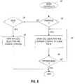
- FIG. 6is a flow chart for one embodiment.
- Electronic threshold switchesare devices whose current voltage (iv) characteristics have a shape similar to that shown in FIG. 5 . Starting from an off state, very little current flows as the voltage is applied until the threshold voltage V th is reached. At this point, the device snaps back and latches to an on state that is much more conductive. A common semiconductor device that exhibits this behavior is a thyristor. Another example is a phase change memory cell whose current voltage curve is shown in FIG. 5 .
- the phase change memory cell whose iv curve is shown in FIG. 5is a threshold switch whose threshold voltage can be programmed and retained.
- some phase change memoriesIn the crystalline or set state, indicated by blackened squares in FIG. 5 , some phase change memories have zero threshold voltage, meaning that they exhibit no thresholding behavior and proceed immediately into the conductive state.
- the threshold voltageIn the amorphous, or reset state, indicated by the open squares in FIG. 5 , the threshold voltage typically depends on how much current was applied during the programming pulse that placed the cell in the reset state. The current during programming may be in the reset current regime, indicated in FIG. 5 . Higher programming current leads to higher threshold voltage, up to a saturation point.
- the maximum voltage available during programmingis limited to a level below the desired reset threshold voltage. Cells whose reset threshold voltage already exceed this threshold voltage do not threshold or receive another programming pulse. In effect, verification is completed before programming is done and only cells that do not verify during programming receive one or more additional programming pulses.
- the cell 20may be a phase change memory cell or any other electronic threshold switch. In one embodiment, it may be a series combination of a phase change memory element and one or more select devices, such as thin film selectors including chalcogenide threshold switches (sometimes called ovonic threshold switches), that normally remain in the amorphous state, and silicon diodes.
- the cell 20is coupled to a transistor 18 whose gate is connected to a cell selection block 14 .
- the cell selection block 14outputs a signal VGtop, which drives the gate of the top transistor 18 .
- the drain of the transistor 18is coupled to a supply voltage and its source is coupled to the cell 20 .
- a current control block 16outputs the signal VGbot, which supplies the gate voltage to a bottom transistor 22 whose drain is coupled to the cell 20 and whose source is coupled to ground.
- the output current from the source of the transistor 22is the current I cell .
- the cell selection block 14 and the current control block 16are driven by a write controller 12 .
- the write controller 12controls the cell selection block 14 and the current control block 16 .
- the net effect of this controlis to control the voltage across the cell 20 .
- the write controller 12can control the voltage across the cell 20 to control programming in a programming mode.
- the write controller 12can also turn off the transistors 18 and 22 to enter a read mode.
- the read circuit 24which may include a sense amplifier, detects the state of the cell 20 which typically is either set or reset. However, multilevel cells may also be used.
- a current detector 26may be used to shorten the programming cycle when possible.
- the transistor 18is biased as a source follower so that its source is an offset version of its gate voltage.
- the transistor 22may be biased as a current mirror, so that its gate voltage translates to programming current I cell . If the threshold voltage of the cell 20 is below the source voltage of the source follower transistor 18 , the cell 20 thresholds, conducts current and, as a result, receives a programming pulse whose current is determined by the current mirror transistor 22 .
- FIGS. 2-4An example of possible waveforms is shown in FIGS. 2-4 with arbitrary scales on both the x and y axes.
- the first pulse, shown at time A in FIG. 4need not threshold the cell. If the cell does not threshold, it means that it already has a high enough threshold voltage. This can avoid unnecessarily resetting cells that are already reset.
- Subsequent current pulses D and Ecan occur at times B and C as needed. These pulses may be considered as conditional in that they only occur if the preceding pulse(s) did not program the threshold voltage of the cell above the corresponding transistor 18 source voltage.
- the transistor 18 gate voltage pulsesare shown in decreasing magnitude at times A-C in FIG. 2 .
- FIG. 2shows the voltage applied to the gate of the transistor 18 at times A, B, and C
- FIG. 3shows the voltage applied to the gate of the transistor 22 at times A, B, and C in one example.
- the gate voltage applied to the transistor 18 gatedecreases with time, while the voltage applied to the transistor 22 gate increases with time.
- This increasing and decreasing magnitudeis not necessary but may lend confidence that a cell is not disturbed to a lower threshold voltage when a voltage is applied and no pulse occurs.
- Each sequential programming pulseis shown as developing increasing current I cell in FIG. 4 , but could also decrease or to change width or edge rate if the cell requires lower current or a different pulse shape for higher threshold voltages.
- the gate voltage of that transistortranslates directly to the voltage on the top node of the cell 20 .
- the cell 20may leak so little current that regardless of the value of the gate voltage of the transistor 22 , the bottom node of the cell 20 is at ground. Under these conditions, the voltage across the cell during each VGtop pulse is the value of VGtop.
- VGtop at time A in FIG. 2has a magnitude of 1.2 volts
- a cell with the I-V curve of FIG. 5thresholds, regardless of its state. After thresholding, the cell conducts a current, as determined by the gate voltage VGbot of the bottom clamp transistor 22 in FIG. 1 .
- FIG. 5shows that with 1.2 volts across the cell, the current in the on state exceeds the range of the y axis, the extra voltage is absorbed by the bottom transistor 22 in saturation.
- the first pulse of VGbotis equal to 0.5, which allows a normalized programming current of 1.2 I/I reset . This is enough to reset a typical cell.
- the second VGtop pulse at time Bshown in FIG. 2 , hypothetically has a magnitude of one volt. If the previous pulse (at time A) successfully reset the cell, then FIG. 5 indicates that one volt is not enough to threshold the cell. Thus, the programming current I cell does not flow. If, however, the previous pulse does reset the bit so that its threshold voltage is less than one volt, the second pulse does not threshold the bit and causes 1.4 I/I reset current to flow. Likewise, if 1.4 I/I reset is not enough, the third pulse at time C does threshold the cell and sends 1.6 I/I rest current into the cell.
- some embodimentsmay be adapted to different threshold voltage programming tendencies. For example, if higher threshold voltage results from a lower magnitude or longer trailing current pulses, a current pulse shaping circuit or algorithm can be changed to provide such pulses after the cell enters the reset current regime. In addition, cells that have zero threshold voltage, because they exhibit snapback, even the set state may be utilized. In some embodiments, cells of this type may exhibit a better margin.
- programming pulsesmay be applied to cells that fail to threshold above a certain value with inverted logic.
- a set pulsemay be applied only after it has been determined that a cell did not threshold.
- the threshold voltage verificationis completed during programming with no explicit sensing operation.
- the circuit and cellimplicitly decide whether or not to deliver a reset pulse. This may simplify the circuitry and speed up the write operation in some embodiments.
- a write algorithmuses multiple write and verify iterations to ensure all cells are programmed to a minimum threshold voltage. Some embodiments allow more flexibility in the current magnitudes used in an algorithm, allowing it to handle a wider spread of cell performance or increase the write speed and bandwidth of a product.
- the write controller 12will attempt to apply a given number of write pulses, regardless of whether they are needed.
- the write controllermay programmably apply two or more pulses. However, if the cell is already programmed, the attempt to provide the additional pulses will be futile. No pulse will be provided, but some time may be used in attempting to apply one or more additional pulses that are not needed.
- the current detector 26may be used to determine if current actually flows. If current does not flow, it can be determined that the cell is already programmed and it is not necessary to apply ensuing pulses. In some embodiments, this may shorten the programming time.
- the write controller 30may implement a sequence to program the cell 22 .
- This sequencemay be implemented in software, hardware, or firmware in some embodiments.
- the write controllermay be a processor-based device that stores instructions in a suitable semiconductor storage device. When those instructions are executed, the write controller can cause a series of operations, described in FIG. 6 , to occur.
- the write controller 12 or some other portion of the memorymay include a computer readable medium storing instructions that, when executed, enable the controller to perform a sequence of operations.
- the write controllerinitially determines whether or not a program operation has been requested, for example, from an external memory controller or other processor. If not, a check at diamond 38 determines whether a read mode has been implemented. If a read mode is implemented, the transistors 18 and 22 may be turned off and the read circuit 24 may then be operated by other circuitry or code, as indicated in block 40 .
- the cell selection 14 and current control 16are driven to provide an appropriate pulse, as indicated in block 34 .
- the cellmay be programmed to an appropriate level.
- a check at diamond 36determines whether or not the cell has been programmed to the appropriate level. In one embodiment this can be determined using the current detector 26 . Namely, if no current flows, then the cell is already programmed and it is not necessary to apply additional programming pulses. Otherwise, another pulse is applied and the flow iterates.
- a series connected select devicemay be used to access a memory element, including the phase change material, during programming or reading of memory element.
- the select devicemay be a threshold switch, such as an ovonic threshold switch, that can be made of a chalcogenide alloy that does not exhibit an amorphous to crystalline phase change and which undergoes rapid, electric field initiated change in electrical conductivity that persists only so long as a holding voltage is present.
- a select devicemay operate as a switch that is either “off” or “on” depending on the amount of voltage potential applied across the memory cell, and more particularly whether the current through the select device exceeds its threshold current or voltage, which then triggers the device into the on state.
- the off statemay be a substantially electrically nonconductive state and the on state may be a substantially conductive state, with less resistance than the off state.
- a select devicemay have threshold voltages and, if a voltage potential less than the threshold voltage of a select device is applied across the select device, then the select device may remain “off” or in a relatively high resistive state so that little or no electrical current passes through the memory cell and most of the voltage drop from selected row to selected column is across the select device.
- the select devicemay “turn on,” i.e., operate in a relatively low resistive state so that electrical current passes through the memory cell.
- one or more series connected select devicesmay be in a substantially electrically nonconductive state if less than a predetermined voltage potential, e.g., the threshold voltage, is applied across select devices.
- Select devicesmay be in a substantially conductive state if greater than the predetermined voltage potential is applied across select devices.
- Select devicesmay also be referred to as an access device, an isolation device, or a switch.
- each select devicemay comprise a switching material such as, for example, a chalcogenide alloy, and may be referred to as an ovonic threshold switch, or simply an ovonic switch.
- the switching material of select devicesmay be a material in a substantially amorphous state positioned between two electrodes that may be repeatedly and reversibly switched between a higher resistance “off” state (e.g., greater than about ten megaOhms) and a relatively lower resistance “on” state (e.g., about one thousand Ohms in series with V H ) by application of a predetermined electrical current or voltage potential.
- each select devicemay be a two terminal device that may have a current-voltage (I-V) characteristic similar to a phase change memory element that is in the amorphous state.
- the switching material of select devicesmay not change phase. That is, the switching material of select devices may not be a programmable material, and, as a result, select devices may not be a memory device capable of storing information. For example, the switching material of select devices may remain permanently amorphous and the I-V characteristic may remain the same throughout the operating life.
- a select deviceIn the low voltage or low electric field mode, i.e., where the voltage applied across select device is less than a threshold voltage (labeled V TH ), a select device may be “off” or nonconducting, and exhibit a relatively high resistance, e.g., greater than about 10 megaOhms. The select device may remain in the off state until a sufficient voltage, e.g., V TH , is applied, or a sufficient current is applied, e.g., I TH , that may switch the select device to a conductive, relatively low resistance on state. After a voltage potential of greater than about V TH is applied across the select device, the voltage potential across the select device may drop (“snapback”) to a holding voltage potential, V H . Snapback may refer to the voltage difference between V TH and V H of a select device.
- the voltage potential across select devicemay remain close to the holding voltage of V H as current passing through select device is increased.
- the select devicemay remain on until the current through the select device drops below a holding current, I H . Below this value, the select device may turn off and return to a relatively high resistance, nonconductive off state until the V TH and I TH are exceeded again.
- the threshold current of the memory elementmay be about equal to the threshold current of the access device even though its snapback voltage is greater than the memory element's reset bit threshold voltage.
- references throughout this specification to “one embodiment” or “an embodiment”mean that a particular feature, structure, or characteristic described in connection with the embodiment is included in at least one implementation encompassed within the present invention. Thus, appearances of the phrase “one embodiment” or “in an embodiment” are not necessarily referring to the same embodiment. Furthermore, the particular features, structures, or characteristics may be instituted in other suitable forms other than the particular embodiment illustrated and all such forms may be encompassed within the claims of the present application.
Landscapes
- Chemical & Material Sciences (AREA)
- Crystallography & Structural Chemistry (AREA)
- Semiconductor Memories (AREA)
Abstract
Description
Claims (23)
Priority Applications (1)
| Application Number | Priority Date | Filing Date | Title |
|---|---|---|---|
| US12/333,518US8031516B2 (en) | 2008-12-12 | 2008-12-12 | Writing memory cells exhibiting threshold switch behavior |
Applications Claiming Priority (1)
| Application Number | Priority Date | Filing Date | Title |
|---|---|---|---|
| US12/333,518US8031516B2 (en) | 2008-12-12 | 2008-12-12 | Writing memory cells exhibiting threshold switch behavior |
Publications (2)
| Publication Number | Publication Date |
|---|---|
| US20100149856A1 US20100149856A1 (en) | 2010-06-17 |
| US8031516B2true US8031516B2 (en) | 2011-10-04 |
Family
ID=42240313
Family Applications (1)
| Application Number | Title | Priority Date | Filing Date |
|---|---|---|---|
| US12/333,518Active2029-05-08US8031516B2 (en) | 2008-12-12 | 2008-12-12 | Writing memory cells exhibiting threshold switch behavior |
Country Status (1)
| Country | Link |
|---|---|
| US (1) | US8031516B2 (en) |
Cited By (8)
| Publication number | Priority date | Publication date | Assignee | Title |
|---|---|---|---|---|
| US20120155161A1 (en)* | 2010-12-21 | 2012-06-21 | Jong-Won Lee | Three-terminal ovonic threshold switch as a current driver in a phase change memory |
| US9390768B2 (en) | 2011-08-18 | 2016-07-12 | Micron Technology, Inc. | Apparatuses, devices and methods for sensing a snapback event in a circuit |
| US9837154B2 (en) | 2015-04-15 | 2017-12-05 | Hewlett Packard Enterprise Development Lp | Resistive random access memory (RRAM) system |
| US10262735B2 (en)* | 2011-03-11 | 2019-04-16 | Ovonyx Memory Technology, Inc. | Devices and methods to program a memory cell |
| US10855087B1 (en) | 2004-01-15 | 2020-12-01 | Comarco Wireless Systems Llc | Power supply systems |
| US11024355B1 (en) | 2020-01-31 | 2021-06-01 | International Business Machines Corporation | MRAM bit line write control with source follower |
| US11177009B2 (en)* | 2019-12-30 | 2021-11-16 | Micron Technology, Inc. | Multi-state programming of memory cells |
| US11315633B2 (en)* | 2019-12-30 | 2022-04-26 | Micron Technology, Inc. | Three-state programming of memory cells |
Families Citing this family (19)
| Publication number | Priority date | Publication date | Assignee | Title |
|---|---|---|---|---|
| US7974119B2 (en) | 2008-07-10 | 2011-07-05 | Seagate Technology Llc | Transmission gate-based spin-transfer torque memory unit |
| US7936580B2 (en) | 2008-10-20 | 2011-05-03 | Seagate Technology Llc | MRAM diode array and access method |
| US9030867B2 (en)* | 2008-10-20 | 2015-05-12 | Seagate Technology Llc | Bipolar CMOS select device for resistive sense memory |
| US7936583B2 (en) | 2008-10-30 | 2011-05-03 | Seagate Technology Llc | Variable resistive memory punchthrough access method |
| US7825478B2 (en)* | 2008-11-07 | 2010-11-02 | Seagate Technology Llc | Polarity dependent switch for resistive sense memory |
| US8178864B2 (en) | 2008-11-18 | 2012-05-15 | Seagate Technology Llc | Asymmetric barrier diode |
| US8203869B2 (en) | 2008-12-02 | 2012-06-19 | Seagate Technology Llc | Bit line charge accumulation sensing for resistive changing memory |
| US8159856B2 (en) | 2009-07-07 | 2012-04-17 | Seagate Technology Llc | Bipolar select device for resistive sense memory |
| US7936585B2 (en)* | 2009-07-13 | 2011-05-03 | Seagate Technology Llc | Non-volatile memory cell with non-ohmic selection layer |
| US8158964B2 (en) | 2009-07-13 | 2012-04-17 | Seagate Technology Llc | Schottky diode switch and memory units containing the same |
| KR101528209B1 (en) | 2010-11-19 | 2015-06-11 | 휴렛-팩커드 디벨롭먼트 컴퍼니, 엘.피. | Method and circuit for switching a memristive device in an array |
| US8648426B2 (en) | 2010-12-17 | 2014-02-11 | Seagate Technology Llc | Tunneling transistors |
| KR102469172B1 (en)* | 2016-03-14 | 2022-11-22 | 에스케이하이닉스 주식회사 | Nonvolatile memory apparatus and verify write method |
| US10381075B2 (en) | 2017-12-14 | 2019-08-13 | Micron Technology, Inc. | Techniques to access a self-selecting memory device |
| US10546632B2 (en)* | 2017-12-14 | 2020-01-28 | Micron Technology, Inc. | Multi-level self-selecting memory device |
| US10755781B2 (en)* | 2018-06-06 | 2020-08-25 | Micron Technology, Inc. | Techniques for programming multi-level self-selecting memory cell |
| US11139025B2 (en) | 2020-01-22 | 2021-10-05 | International Business Machines Corporation | Multi-level cell threshold voltage operation of one-selector-one-resistor structure included in a crossbar array |
| US11217308B1 (en) | 2020-08-14 | 2022-01-04 | Micron Technology | Programming memory cells using asymmetric current pulses |
| US12249369B2 (en)* | 2021-07-09 | 2025-03-11 | Taiwan Semiconductor Manufacturing Company, Ltd. | Adjusting operation voltage of cross point memory according to aging information |
Citations (8)
| Publication number | Priority date | Publication date | Assignee | Title |
|---|---|---|---|---|
| US6487113B1 (en)* | 2001-06-29 | 2002-11-26 | Ovonyx, Inc. | Programming a phase-change memory with slow quench time |
| US6667900B2 (en)* | 2001-12-28 | 2003-12-23 | Ovonyx, Inc. | Method and apparatus to operate a memory cell |
| US6768665B2 (en)* | 2002-08-05 | 2004-07-27 | Intel Corporation | Refreshing memory cells of a phase change material memory device |
| US6859390B2 (en)* | 2002-09-23 | 2005-02-22 | Ovonyx, Inc. | Phase-change memory element and method of storing data therein |
| US7050328B2 (en)* | 2001-12-27 | 2006-05-23 | Stmicroelectronics S.R.L. | Phase change memory device |
| US20060181931A1 (en)* | 2003-08-13 | 2006-08-17 | Ha Yong-Ho | Method and driver for programming phase change memory cell |
| US20070115749A1 (en)* | 2005-10-14 | 2007-05-24 | Axon Technologies Corporation | Voltage reference circuit using programmable metallization cells |
| US20090103365A1 (en)* | 2007-10-18 | 2009-04-23 | Micron Technology, Inc. | Sensing of memory cells in NAND flash |
- 2008
- 2008-12-12USUS12/333,518patent/US8031516B2/enactiveActive
Patent Citations (9)
| Publication number | Priority date | Publication date | Assignee | Title |
|---|---|---|---|---|
| US6487113B1 (en)* | 2001-06-29 | 2002-11-26 | Ovonyx, Inc. | Programming a phase-change memory with slow quench time |
| US7050328B2 (en)* | 2001-12-27 | 2006-05-23 | Stmicroelectronics S.R.L. | Phase change memory device |
| US7324371B2 (en)* | 2001-12-27 | 2008-01-29 | Stmicroelectronics S.R.L. | Method of writing to a phase change memory device |
| US6667900B2 (en)* | 2001-12-28 | 2003-12-23 | Ovonyx, Inc. | Method and apparatus to operate a memory cell |
| US6768665B2 (en)* | 2002-08-05 | 2004-07-27 | Intel Corporation | Refreshing memory cells of a phase change material memory device |
| US6859390B2 (en)* | 2002-09-23 | 2005-02-22 | Ovonyx, Inc. | Phase-change memory element and method of storing data therein |
| US20060181931A1 (en)* | 2003-08-13 | 2006-08-17 | Ha Yong-Ho | Method and driver for programming phase change memory cell |
| US20070115749A1 (en)* | 2005-10-14 | 2007-05-24 | Axon Technologies Corporation | Voltage reference circuit using programmable metallization cells |
| US20090103365A1 (en)* | 2007-10-18 | 2009-04-23 | Micron Technology, Inc. | Sensing of memory cells in NAND flash |
Cited By (23)
| Publication number | Priority date | Publication date | Assignee | Title |
|---|---|---|---|---|
| US10855087B1 (en) | 2004-01-15 | 2020-12-01 | Comarco Wireless Systems Llc | Power supply systems |
| US11586233B2 (en) | 2004-01-15 | 2023-02-21 | Comarco Wireless Systems Llc | Power supply systems |
| US10951042B2 (en) | 2004-01-15 | 2021-03-16 | Comarco Wireless Systems Llc | Power supply systems |
| US10855086B2 (en) | 2004-01-15 | 2020-12-01 | Comarco Wireless Systems Llc | Power supply equipment utilizing interchangeable tips to provide power and a data signal to electronic devices |
| US8345472B2 (en)* | 2010-12-21 | 2013-01-01 | Intel Corporation | Three-terminal ovonic threshold switch as a current driver in a phase change memory |
| US20120155161A1 (en)* | 2010-12-21 | 2012-06-21 | Jong-Won Lee | Three-terminal ovonic threshold switch as a current driver in a phase change memory |
| US11120873B2 (en) | 2011-03-11 | 2021-09-14 | Ovonyx Memory Technology, Llc | Devices and methods to program a memory cell |
| US10262735B2 (en)* | 2011-03-11 | 2019-04-16 | Ovonyx Memory Technology, Inc. | Devices and methods to program a memory cell |
| US10706926B2 (en) | 2011-03-11 | 2020-07-07 | Ovonyx Memory Technology, Llc | Devices and methods to program a memory cell |
| US10083745B2 (en) | 2011-08-18 | 2018-09-25 | Micron Technology, Inc | Apparatuses, devices and methods for sensing a snapback event in a circuit |
| US10636483B2 (en) | 2011-08-18 | 2020-04-28 | Micron Technology, Inc. | Apparatuses, devices and methods for sensing a snapback event in a circuit |
| US9390768B2 (en) | 2011-08-18 | 2016-07-12 | Micron Technology, Inc. | Apparatuses, devices and methods for sensing a snapback event in a circuit |
| US11100991B2 (en) | 2011-08-18 | 2021-08-24 | Micron Technology, Inc. | Apparatuses, devices and methods for sensing a snapback event in a circuit |
| US9747981B2 (en) | 2011-08-18 | 2017-08-29 | Micron Technology, Inc. | Apparatuses, devices and methods for sensing a snapback event in a circuit |
| US9837154B2 (en) | 2015-04-15 | 2017-12-05 | Hewlett Packard Enterprise Development Lp | Resistive random access memory (RRAM) system |
| US11315633B2 (en)* | 2019-12-30 | 2022-04-26 | Micron Technology, Inc. | Three-state programming of memory cells |
| US11177009B2 (en)* | 2019-12-30 | 2021-11-16 | Micron Technology, Inc. | Multi-state programming of memory cells |
| US20220246210A1 (en)* | 2019-12-30 | 2022-08-04 | Micron Technology, Inc. | Three-state programming of memory cells |
| US11869588B2 (en)* | 2019-12-30 | 2024-01-09 | Micron Technology, Inc. | Three-state programming of memory cells |
| US20240120006A1 (en)* | 2019-12-30 | 2024-04-11 | Micron Technology, Inc. | Three-state programming of memory cells |
| US11989228B2 (en) | 2019-12-30 | 2024-05-21 | Micron Technology, Inc. | Multi-state programming of memory cells |
| US12374408B2 (en) | 2019-12-30 | 2025-07-29 | Micron Technology, Inc. | Multi-state programming of memory cells |
| US11024355B1 (en) | 2020-01-31 | 2021-06-01 | International Business Machines Corporation | MRAM bit line write control with source follower |
Also Published As
| Publication number | Publication date |
|---|---|
| US20100149856A1 (en) | 2010-06-17 |
Similar Documents
| Publication | Publication Date | Title |
|---|---|---|
| US8031516B2 (en) | Writing memory cells exhibiting threshold switch behavior | |
| KR100764738B1 (en) | Phase change memory device with improved reliability, its writing method, and system including it | |
| US8305793B2 (en) | Integrated circuit with an array of resistance changing memory cells | |
| US6940744B2 (en) | Adaptive programming technique for a re-writable conductive memory device | |
| US7259982B2 (en) | Reading phase change memories to reduce read disturbs | |
| EP3304560B1 (en) | Phase change memory current | |
| US20110188292A1 (en) | Variable resistance memory, operating method and system | |
| US8614911B2 (en) | Energy-efficient row driver for programming phase change memory | |
| US10311921B1 (en) | Multiple-mode current sources for sense operations | |
| US11232836B2 (en) | Resistive random access memory device | |
| WO2007075392A1 (en) | Writing phase change memories | |
| US20130051139A1 (en) | Resetting Phase Change Memory Bits | |
| US12361988B2 (en) | Adaptive write operations for a memory device | |
| US10553644B2 (en) | Test circuit block, variable resistance memory device including the same, and method of forming the variable resistance memory device | |
| KR102471567B1 (en) | Memory device and method for controlling the memory device | |
| US11705197B2 (en) | Modified write voltage for memory devices | |
| TWI622997B (en) | Memory device, system and operating method thereof |
Legal Events
| Date | Code | Title | Description |
|---|---|---|---|
| AS | Assignment | Owner name:NUMONYX B.V.,SWITZERLAND Free format text:ASSIGNMENT OF ASSIGNORS INTEREST;ASSIGNOR:TANG, STEPHEN;REEL/FRAME:024601/0026 Effective date:20081211 Owner name:NUMONYX B.V., SWITZERLAND Free format text:ASSIGNMENT OF ASSIGNORS INTEREST;ASSIGNOR:TANG, STEPHEN;REEL/FRAME:024601/0026 Effective date:20081211 | |
| STCF | Information on status: patent grant | Free format text:PATENTED CASE | |
| FEPP | Fee payment procedure | Free format text:PAYOR NUMBER ASSIGNED (ORIGINAL EVENT CODE: ASPN); ENTITY STATUS OF PATENT OWNER: LARGE ENTITY | |
| FPAY | Fee payment | Year of fee payment:4 | |
| MAFP | Maintenance fee payment | Free format text:PAYMENT OF MAINTENANCE FEE, 8TH YEAR, LARGE ENTITY (ORIGINAL EVENT CODE: M1552); ENTITY STATUS OF PATENT OWNER: LARGE ENTITY Year of fee payment:8 | |
| MAFP | Maintenance fee payment | Free format text:PAYMENT OF MAINTENANCE FEE, 12TH YEAR, LARGE ENTITY (ORIGINAL EVENT CODE: M1553); ENTITY STATUS OF PATENT OWNER: LARGE ENTITY Year of fee payment:12 |