US8021723B2 - Method of plasma treatment using amplitude-modulated RF power - Google Patents
Method of plasma treatment using amplitude-modulated RF powerDownload PDFInfo
- Publication number
- US8021723B2 US8021723B2US11/946,022US94602207AUS8021723B2US 8021723 B2US8021723 B2US 8021723B2US 94602207 AUS94602207 AUS 94602207AUS 8021723 B2US8021723 B2US 8021723B2
- Authority
- US
- United States
- Prior art keywords
- power
- modulated
- amplitude
- substrate
- film
- Prior art date
- Legal status (The legal status is an assumption and is not a legal conclusion. Google has not performed a legal analysis and makes no representation as to the accuracy of the status listed.)
- Active, expires
Links
- 238000000034methodMethods0.000titleclaimsabstractdescription66
- 238000009832plasma treatmentMethods0.000titledescription2
- 239000000758substrateSubstances0.000claimsabstractdescription83
- 238000012545processingMethods0.000claimsabstractdescription18
- 238000005268plasma chemical vapour depositionMethods0.000claimsabstractdescription11
- 239000007789gasSubstances0.000claimsdescription59
- 230000015572biosynthetic processEffects0.000claimsdescription13
- 239000000654additiveSubstances0.000claimsdescription12
- 230000000996additive effectEffects0.000claimsdescription12
- 239000012159carrier gasSubstances0.000claimsdescription6
- 230000008033biological extinctionEffects0.000claims1
- 230000008569processEffects0.000description25
- 230000003247decreasing effectEffects0.000description14
- 239000012495reaction gasSubstances0.000description11
- 239000004065semiconductorSubstances0.000description10
- 230000008901benefitEffects0.000description7
- 238000010438heat treatmentMethods0.000description6
- 230000007246mechanismEffects0.000description4
- 230000003647oxidationEffects0.000description3
- 238000007254oxidation reactionMethods0.000description3
- 230000000052comparative effectEffects0.000description2
- 238000010586diagramMethods0.000description2
- 230000000694effectsEffects0.000description2
- 238000004381surface treatmentMethods0.000description2
- MYMOFIZGZYHOMD-UHFFFAOYSA-NDioxygenChemical compoundO=OMYMOFIZGZYHOMD-UHFFFAOYSA-N0.000description1
- BOTDANWDWHJENH-UHFFFAOYSA-NTetraethyl orthosilicateChemical compoundCCO[Si](OCC)(OCC)OCCBOTDANWDWHJENH-UHFFFAOYSA-N0.000description1
- 230000002411adverseEffects0.000description1
- 230000003466anti-cipated effectEffects0.000description1
- 230000008859changeEffects0.000description1
- 238000006243chemical reactionMethods0.000description1
- 230000007423decreaseEffects0.000description1
- 229910001882dioxygenInorganic materials0.000description1
- 238000002474experimental methodMethods0.000description1
- 230000002209hydrophobic effectEffects0.000description1
- 239000011261inert gasSubstances0.000description1
- 238000009413insulationMethods0.000description1
- 238000000691measurement methodMethods0.000description1
- 239000000203mixtureSubstances0.000description1
- 238000012986modificationMethods0.000description1
- 230000004048modificationEffects0.000description1
- 229910052814silicon oxideInorganic materials0.000description1
- 239000000126substanceSubstances0.000description1
- 238000012546transferMethods0.000description1
Images


Classifications
- H—ELECTRICITY
- H01—ELECTRIC ELEMENTS
- H01J—ELECTRIC DISCHARGE TUBES OR DISCHARGE LAMPS
- H01J37/00—Discharge tubes with provision for introducing objects or material to be exposed to the discharge, e.g. for the purpose of examination or processing thereof
- H01J37/32—Gas-filled discharge tubes
- H01J37/32009—Arrangements for generation of plasma specially adapted for examination or treatment of objects, e.g. plasma sources
- H01J37/32082—Radio frequency generated discharge
- H01J37/32137—Radio frequency generated discharge controlling of the discharge by modulation of energy
- H01J37/32146—Amplitude modulation, includes pulsing
- C—CHEMISTRY; METALLURGY
- C23—COATING METALLIC MATERIAL; COATING MATERIAL WITH METALLIC MATERIAL; CHEMICAL SURFACE TREATMENT; DIFFUSION TREATMENT OF METALLIC MATERIAL; COATING BY VACUUM EVAPORATION, BY SPUTTERING, BY ION IMPLANTATION OR BY CHEMICAL VAPOUR DEPOSITION, IN GENERAL; INHIBITING CORROSION OF METALLIC MATERIAL OR INCRUSTATION IN GENERAL
- C23C—COATING METALLIC MATERIAL; COATING MATERIAL WITH METALLIC MATERIAL; SURFACE TREATMENT OF METALLIC MATERIAL BY DIFFUSION INTO THE SURFACE, BY CHEMICAL CONVERSION OR SUBSTITUTION; COATING BY VACUUM EVAPORATION, BY SPUTTERING, BY ION IMPLANTATION OR BY CHEMICAL VAPOUR DEPOSITION, IN GENERAL
- C23C16/00—Chemical coating by decomposition of gaseous compounds, without leaving reaction products of surface material in the coating, i.e. chemical vapour deposition [CVD] processes
- C23C16/44—Chemical coating by decomposition of gaseous compounds, without leaving reaction products of surface material in the coating, i.e. chemical vapour deposition [CVD] processes characterised by the method of coating
- C23C16/50—Chemical coating by decomposition of gaseous compounds, without leaving reaction products of surface material in the coating, i.e. chemical vapour deposition [CVD] processes characterised by the method of coating using electric discharges
- C23C16/505—Chemical coating by decomposition of gaseous compounds, without leaving reaction products of surface material in the coating, i.e. chemical vapour deposition [CVD] processes characterised by the method of coating using electric discharges using radio frequency discharges
- H—ELECTRICITY
- H01—ELECTRIC ELEMENTS
- H01J—ELECTRIC DISCHARGE TUBES OR DISCHARGE LAMPS
- H01J37/00—Discharge tubes with provision for introducing objects or material to be exposed to the discharge, e.g. for the purpose of examination or processing thereof
- H01J37/32—Gas-filled discharge tubes
- H01J37/32009—Arrangements for generation of plasma specially adapted for examination or treatment of objects, e.g. plasma sources
- H01J37/32082—Radio frequency generated discharge
- H01J37/32091—Radio frequency generated discharge the radio frequency energy being capacitively coupled to the plasma
Definitions
- the present inventiongenerally relates to semiconductor processing in a plasma treatment apparatus, particularly to a method of reducing a floating potential of a substrate upon film formation.
- a floating voltageis generated on a substrate placed on a substrate processing base while film is being formed. This substrate voltage remains in the substrate after the film forming process has completed, and may sometimes cause the substrate to be attracted to the substrate processing base, in which case a problem will occur in the subsequent process of transferring the substrate.
- the sticking force that applies between the wafer and electrodeis expressed by the formula below:
- F (N)indicates the sticking force
- ⁇ 0 (F/m)indicates the dielectric constant in vacuum
- ⁇ rindicates the specific dielectric constant of anodic oxidation
- S (m 2 )indicates the wafer area
- V w (V)indicates the floating potential of the wafer
- d (m)indicates the thickness of film generated by anodic oxidation.
- the aforementioned methodpresents problems in that it cannot lower the substrate voltage sufficiently if an increased number of substrates are processed, or under different substrate conditions such as when different types of fine processing have been applied to the substrate or depending on whether or not an insulation film is formed on the back of the substrate, in which case the substrate will still be attracted to the substrate processing base and proper transfer will be prevented.
- only a gas that does not form filmis supplied and a high-frequency power that has been amplitude-modulated is applied to cause discharge, in order to reduce the floating potential of the substrate after the film forming process has completed, thereby solving at least one of the aforementioned problems.
- the substrate voltagecan be lowered sufficiently after the end of the process, which virtually eliminates the problem of unwanted substrate sticking or reduces such sticking significantly.
- the time needed to reduce the floating potential of the substratecan be shortened, which has the effect of improving the productivity.
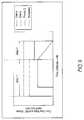
- FIG. 1is a schematic diagram of a plasma CVD apparatus for conducting an embodiment of the present invention.
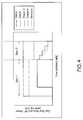
- FIG. 2is a graph showing operation patterns of control parameters in an embodiment of the present invention wherein amplitude-modulated RF power is applied constantly.
- FIG. 3is a graph showing operation patterns of control parameters in an embodiment of the present invention wherein amplitude-modulated RF power is ramped down.
- FIG. 4is a graph showing operation patterns of control parameters in embodiments of the present invention wherein amplitude-modulated RF power is reduced in steps, and amplitude-modulated RF power is reduced at different rates.
- FIG. 5is a graph showing operation patterns of control parameters wherein various post-film forming RF power applications are employed in Comparative Examples and Examples of the present invention.
- the present inventionprovides a method for processing a substrate by plasma CVD, comprising: (i) forming a film on a substrate placed on a susceptor by applying RF power between the susceptor and a shower plate in the presence of a film-forming gas in a reactor; and (ii) upon completion of step (i), without unloading the substrate, applying amplitude-modulated RF power between the susceptor and the shower plate in the absence of a film-forming gas but in the presence of a non-film-forming gas to reduce a floating potential of the substrate.
- the film forming step (step (i))may include a surface treatment step wherein the surface of the substrate is treated using a plasma while substantially or nearly no film is formed in order to change chemical properties of the surface, e.g., changing hydrophilic or hydrophobic properties.
- the methodmay further comprise unloading the substrate upon completion of step (ii), and step (ii) may be initiated immediately before unloading the substrate or as a last step before unloading the substrate. Between step (i) and step (ii), preferably, a plasma is not extinct and remains even at a low density.
- the amplitude-modulated RF power used in step (ii)may be constant and may have an electric power equal to or lower than the electric power of the RF power used in step (i).
- a square root of amplitudecorresponds to power, and thus, strictly speaking, the amplitude-modulated RF power cannot be constant.
- the frequency of amplitude modulationmay be in a range of low frequencies or intermediate frequencies and is relatively so high that fluctuation of amplitude is negligible as compared with the frequency of the RF power itself.
- the RF power which is to be amplitude-modulatedis used to indicate the amplitude-modulated RF power, since the amplitude-modulated RF power is generated by amplitude-modulating the RF power with an amplitude modulator.
- the amplitude modulatoris typically but not necessarily in an on or off state, and when amplitude-modulating the RF power, the amplitude modulator is turned on.
- the amplitude-modulated RF power used in step (ii)may be ramped down continuously. Ramp rates may be such that if ramping continues, power is reduced to zero within 10 seconds (e.g., 7 seconds, 5 seconds).
- the amplitude-modulated RF powermay be reduced toward the end of step (ii) in a step or steps, in pulses, at rates decreasing or increasing with time, at a constant rate, or any two or more of the foregoing in combination.
- step (ii)may be performed for 2 seconds or more but 10 seconds or less (preferably for 2 seconds or more but 3 seconds or less).
- the amplitude-modulated RF powermay be the sole RF power.
- a combination of the non-modulated RF power and the amplitude-modulated RF powercan be used sequentially or simultaneously.
- the amplitude-modulated RF power used in step (ii)may have an electric power of 5 W to 50 W (including 10 W, 20 W, 30 W, 40 W, and values between any two values of the foregoing).
- the electric powermay be lower than 5 W (e.g., 2 W, 4 W) as long as a plasma is not extinct, and may be higher than 50 W (e.g., 60 W, 80 W, 100 W) as long as an adverse effect occur on a surface of the substrate (normally, lower than the RF power used for film formation).
- the RF power to be amplitude-modulatedmay be 50 W to 3,000 W, depending on the type of process conducted prior to removal of floating potential.
- the amplitude-modulated RF power used in step (ii)may be amplitude-modulated with a sine wave of 100 Hz to 500 kHz (including 500 Hz, 1 kHz, 10 kHz, 100 kHz, 200 kHz, and values between any two numbers of the foregoing, preferably 1 kHz to 10 kHz in an embodiment) and may have an amplitude modulation ratio of 0.25 to 1.2 (including 0.5, 0.75, 1.0, and values between any values of the foregoing, preferably 0.8 to 1.0 in an embodiment).
- the amplitude modulation ratiois defined as (A ⁇ B)/(A+B) wherein A is the highest amplitude, and B is the lowest amplitude.
- the amplitude-modulated RF powermay have a frequency of 2 MHz or higher (e.g., 13.56 MHz).
- the frequencycorresponds to the frequency of the RF power which is to be amplitude-modulated.
- the RF power which is used for film formationmay be used as base RF power which is to be amplitude-modulated, although RF power which is different from the RF power used for film formation can be used.
- combined RF poweris used for film formation (e.g., a mixture of low-frequency RF power and high-frequency RF power)
- only the high-frequency RF powermay be amplitude-modulated and used for removal of floating potential.
- both or either one of the high-frequency RF power and the low-frequency RF powercan be amplitude-modulated.
- the non-film-forming gasmay be at least one selected from the group consisting of N 2 , N 2 O, O 2 , Ar, and He.
- Hcan be used, and in other embodiments, rare gas or inert gas can be used.
- the film-forming gas in step (i)may comprise a source gas and an additive/carrier gas, and the non-film-forming gas in step (ii) may comprise the additive/carrier gas without the source gas.
- O 2 gascan continuously be used for removal of floating potential of the substrate.
- N 2 gascan continuously be used for removal of floating potential of the substrate.
- SiON filmis formed on the substrate
- N 2 O gasmay be used in the film formation step
- N 2 O gascan continuously be used for removal of floating potential of the substrate.
- gas which is not used for film formationcan be used for removal of floating potential of the substrate. Suitable gas can be selected as long as a plasma is generated for removal of floating potential.
- a flow rate of gas used for removal of floating potentialmay be 100 sccm to 3,000 sccm (including 500 sccm, 1,000, sccm, 2,000 sccm, and values between any two values of the foregoing).
- the pressuremay be 1 Torr to 10 Torr (preferably 2 Torr to 6 Torr)
- the temperature of the susceptormay be 300° C. to 650° C. (preferably 350° C. to 450° C.)
- the temperature of the shower platemay be 50° C. to 200° C. (preferably 80° C. to 150° C.).
- the present inventionprovides a method for reducing a floating potential of a substrate on a susceptor in a plasma CVD reactor, comprising: upon completion of processing the substrate in the reactor and before unloading the substrate, applying amplitude-modulated RF power between the susceptor and a shower plate in the absence of a film-forming gas but in the presence of a non-film-forming gas for reducing a floating potential of the substrate to a set level.
- the amplitude-modulated RF powermay have an amplitude modulation ratio of 0.25 to 1.2 (preferably 0.8 to 1.0).
- the amplitude-modulated RF powermay be amplitude-modulated with a sine wave of less than 500 kHz (preferably 1 kHz to 10 kHz).
- the amplitude-modulated RF powermay be generated by amplitude-modulating the RF power which is reduced with time toward the end of the step of applying the amplitude-modulated RF power.
- Various ways to reduce the amplitude-modulated powermay be employed.
- the non-film-forming gasmay be O 2 , N 2 , or N 2 O.
- the non-film-forming gasmay comprise an additive/carrier gas without a source gas used in the film formation.
- the non-film-forming gasmay be a gas which is not used in the film formation.
- the applying of the amplitude-modulated RF powermay be conducted to reduce a floating potential of the substrate to 1 ⁇ 2 or less (including 1 ⁇ 4, 1/7, 1/10, 1/20, and values between any two numbers of the foregoing, preferably 1/10 or less) of a floating potential of the substrate obtained with RF power without the amplitude modulation.
- the amplitude-modulated RF powermay be applied to the shower plate. In an embodiment, the amplitude-modulated RF power may be applied to the susceptor or both the shower plate and the susceptor.
- FIG. 1is a schematic diagram of a plasma CVD apparatus for conducting an embodiment of the present invention.
- reference numeralsdenote the following: 1 : Plasma CVD apparatus; 2 : Reactor; 3 : Substrate-supporting device; 4 : Heating block; 5 : Top plate; 6 : Upper electrode; 7 : showerhead; 8 : Reaction gas flow-in conduit; 9 : Matching circuit; 10 , 10 ′: RF generators; 11 : Semiconductor substrate; 12 : Opening; 13 : Gate valve; 14 : Exhaust opening; 15 : Exhaust pipe; 16 : Heater; 17 : Temperature controller; 18 : Arbitrary waveform generator (amplitude modulator).
- a plasma CVD apparatus 1 used to form a film on a semiconductor substratecomprises: a rector 2 ; a susceptor 3 on which to place a semiconductor substrate 11 ; a showerhead 7 provided in a manner facing the susceptor 3 and used to uniformly inject a reaction gas onto the semiconductor substrate 11 ; a gas flow-in conduit 8 that introduces a gas into the reactor; an exhaust opening 14 that evacuates the interior of the reactor; an opening 12 through which to load/unload the semiconductor substrate 11 into and out of the reactor; one type or two types of high-frequency (RF) generators 10 , 10 ′ used to apply a specified voltage or voltages; and a matching circuit 9 used to maintain the impedance at a specified level.
- RFhigh-frequency
- the opening 12is provided in the side face of the reactor, and the reactor 2 is connected via a gate valve 13 to a loading chamber (not illustrated) used to load and unload a semiconductor substrate 11 .
- the exhaust opening 14is provided inside the reactor 2 , and this exhaust opening 14 is connected to a vacuum evacuation pump (not illustrated) via a pipe 15 .
- a vacuum evacuation pump(not illustrated)
- a mechanism to detect the pressure in the reactorand another mechanism to adjust the pressure, so that by using these mechanisms (not illustrated) the interior of the reactor can be controlled at a specified pressure.
- the showerhead 7is provided in the reactor 2 in a position where the showerhead faces the susceptor 3 .
- This showerhead 7is connected to the reaction gas flow-in conduit 8 used to introduce a reaction gas, and the gas is injected into the reactor 2 through several thousand holes (not illustrated) provided in the bottom surface of the showerhead for the purpose of injecting the reaction gas onto the substrate.
- the showerhead 7is also electrically connected to the RF generators 10 , 10 ′ via the RF matching circuit 9 , to form one electrode 6 used in the implementation of plasma discharge.
- the susceptor 3 provided in the reactor 2 for the purpose of placing a semiconductor 11 on topcomprises a top plate 5 having a placement surface for placing a semiconductor substrate on which an anodic oxidation film has been formed, and a heating block 4 with a built-in heater 16 used to heat the semiconductor substrate.
- the susceptor 3is grounded and forms the other electrode used in the implementation of plasma discharge.
- the top plate 5is detachably affixed to the heating block 4 by means of screws, etc. However, no problem will be anticipated even when the top plate 5 and heating block 4 are joined together.
- the susceptor 3is connected to a drive mechanism (not illustrated) which is provided outside the reactor 2 and used to move the susceptor 3 up and down.
- Installed in the heating block 4is a heater 16 of resistance heating type, which is connected to an external power supply and a temperature controller 17 .
- the heater 16is controlled by the temperature controller 17 in a manner allowing the susceptor 3 to be heated to a desired temperature (between 300° C. and 650° C.).
- the RF generators 10 , 10 ′generate electric power at different frequencies of 13.56 MHz and 430 kHz, respectively, and these two levels of electric power are combined in the matching circuit 9 and the combined electric power is supplied to the reactor.
- the RF generators 10 , 10 ′are connected to an arbitrary waveform generator 18 that generates modulation signals to an outside circuit, so that the generators receive signals from the arbitrary waveform generator 18 and oscillate non-modulated RF power or RF power that has been modulated to an arbitrary waveform.
- the RF generators 10 , 10 ′ and arbitrary waveform generator 18are controlled by the controller of the apparatus.
- a reaction gas and a gas that does not react by itself, gas that does not contribute to any reaction, or any other gasare introduced from the reaction gas flow-in conduit 8 , and the interior of the reactor 2 is maintained at an arbitrary pressure.
- non-modulated RF power having a frequency of 13.56 MHz, or two levels of non-modulated RF power having frequencies of 13.56 MHz and 430 kHzwill be applied to the upper electrode 6 in the reactor 2 through the matching circuit 9 to form a film by means of plasma.
- a film termination process or other process in which electric discharge is implemented by using the additive gas alonemay be performed after the film forming process in order to adjust the film quality.
- the operationis comprised of two steps:
- the first stepis processing a substrate
- the second stepis reducing floating potential of the substrate prior to unloading the substrate.
- the first stepcan comprise multiple steps including film formation steps and surface treatment steps.
- the second stepcan comprise multiple steps as long as the amplitude-modulated RF power is used at least one step in the second step.
- Step 1indicates a film forming process or film termination treatment process
- step 2indicates a process of removing electric charges by means of modulation.
- gas aindicates a reaction gas
- gas bindicates an additive gas.
- Both the vertical and horizontal axesrepresent arbitrary units, and changes along each axis are not scaled. Modulation is expressed by an on/off state.
- the reaction gasis stopped and only the additive gas is supplied after the film forming process or film termination process has completed, and if RF power of 430 kHz is used, then application of the 430-kHz RF power is stopped and RF power of 13.56 MHz alone, which has been adjusted to 20 W, is applied for approx. 3 seconds at a constant electric power to cause discharge.
- the RF poweris amplitude-modulated at a modulation frequency of 5 kHz and amplitude modulation ratio of 1.
- the electric power of 20 Wis used.
- the electric powermay be reduced to, for example, 5 W, as long as plasma is not lost (the specific level of electric power varies depending on the type of each gas used and the structure of the apparatus).
- the RF power frequenciesare set to 13.56 MHz and 430 kHz above, other frequencies may be used in a range of 10 MHz or above but 100 MHz or below, and in a range of 300 kHz or above but 1000 kHz or below, respectively.
- the modulation frequencyneed not be 5 kHz, and any other frequency in a range of 100 Hz to 500 kHz can be used.
- the amplitude modulation ratiomay be set to an arbitrary value within a range of 0.25 to 1.2, instead of 1.
- the period during which the modulated RF power is appliedmay be other than 3 seconds, as long as the period is 2 seconds or more.
- FIG. 3Another example of the present invention is explained below by referring to FIG. 3 .
- Step 1indicates a film forming process or film termination treatment process
- step 2indicates a process of removing electric charges by means of modulation.
- gas aindicates a reaction gas
- gas bindicates an additive gas.
- reaction gasis stopped and only the additive gas is supplied after the film forming process or film termination process has completed, and if RF power of 430 kHz is used, then application of the 430-kHz RF power is stopped and RF power of 13.56 MHz alone is applied for approx. 3 seconds.
- the RF poweris amplitude-modulated at a modulation frequency of 5 kHz and amplitude modulation ratio of 1, and the electric power is gradually decreased from the same level used during the film forming process in such a way that the electric power becomes 0 W when the process ends (the electric power is decreased linearly).
- the modulation frequencyneed not be 5 kHz, and any other frequency in a range of 100 Hz to 500 kHz can be used.
- the amplitude modulation ratiomay be set to an arbitrary value within a range of 0.25 to 1.2, instead of 1.
- the period during which the modulated RF power is appliedmay be other than 3 seconds, as long as the period is 2 seconds or more.
- Example 2Although the electric power is gradually decreased in Example 2 given above, the voltage may be lowered in several steps as shown in FIG. 4 , or the rate at which the voltage is lowered may be changed in each of these steps. It is also possible to combine Examples 1, 2 and/or 3.
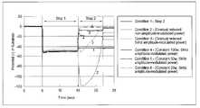
- FIGS. 5 and 6The results of processes performed in Examples 1 and 2 are shown in FIGS. 5 and 6 .
- the apparatus shown in FIG. 1was used to process substrates under the conditions specified in Tables 1 to 3 below, and the resulting floating voltages were measured and compared. (For your information, the floating voltages were measured according to the Vf measurement method disclosed in U.S. patent application Ser. No. 11/847,962, also filed by the same applicant who filed the application for the present invention. The disclosure of the application is herein incorporated by reference in its entirety.)
- FIG. 5shows how the substrate voltage changes over time when the setting of electric power and modulation conditions are changed in step 2.
- FIG. 6shows the substrate voltages measured after completion of processing under respective conditions.
- step 2When the electric power was kept constant in step 2, the substrate voltage measured after the end of step 2 changed according to the electric power in step 2, where the smaller the electric power, the lower the substrate voltage became and the substrate voltage became ⁇ 1.2 V when the electric power was 20 W.
- step 2applying amplitude modulation in step 2 allowed the substrate voltage to be reduced to a sufficiently low level compared to when modulation was not applied.
Landscapes
- Chemical & Material Sciences (AREA)
- Engineering & Computer Science (AREA)
- Physics & Mathematics (AREA)
- Plasma & Fusion (AREA)
- Analytical Chemistry (AREA)
- General Chemical & Material Sciences (AREA)
- Chemical Kinetics & Catalysis (AREA)
- Materials Engineering (AREA)
- Mechanical Engineering (AREA)
- Metallurgy (AREA)
- Organic Chemistry (AREA)
- Chemical Vapour Deposition (AREA)
Abstract
Description
1. Field of the Invention
The present invention generally relates to semiconductor processing in a plasma treatment apparatus, particularly to a method of reducing a floating potential of a substrate upon film formation.
2. Description of the Related Art
In capacity-coupled plasma CVD, a floating voltage is generated on a substrate placed on a substrate processing base while film is being formed. This substrate voltage remains in the substrate after the film forming process has completed, and may sometimes cause the substrate to be attracted to the substrate processing base, in which case a problem will occur in the subsequent process of transferring the substrate.
The sticking force that applies between the wafer and electrode is expressed by the formula below:
Here, F (N) indicates the sticking force, ∈0(F/m) indicates the dielectric constant in vacuum, ∈rindicates the specific dielectric constant of anodic oxidation, S (m2) indicates the wafer area, Vw(V) indicates the floating potential of the wafer, and d (m) indicates the thickness of film generated by anodic oxidation. Based on the above formula, the sticking force can be decreased by lowering Vw.
Traditionally, the method of applying RF power continuously after the film forming process has completed to remove electric charges from the substrate has been used to reduce the sticking force of the wafer and electrode.
However, the aforementioned method presents problems in that it cannot lower the substrate voltage sufficiently if an increased number of substrates are processed, or under different substrate conditions such as when different types of fine processing have been applied to the substrate or depending on whether or not an insulation film is formed on the back of the substrate, in which case the substrate will still be attracted to the substrate processing base and proper transfer will be prevented.
In at least one embodiment of the present invention, only a gas that does not form film is supplied and a high-frequency power that has been amplitude-modulated is applied to cause discharge, in order to reduce the floating potential of the substrate after the film forming process has completed, thereby solving at least one of the aforementioned problems.
In other words, in at least one embodiment of the present invention the substrate voltage can be lowered sufficiently after the end of the process, which virtually eliminates the problem of unwanted substrate sticking or reduces such sticking significantly. Furthermore, in an embodiment of the present invention the time needed to reduce the floating potential of the substrate can be shortened, which has the effect of improving the productivity.
For purposes of summarizing the invention and the advantages achieved over the related art, certain objects and advantages of the invention are described in this disclosure. Of course, it is to be understood that not necessarily all such objects or advantages may be achieved in accordance with any particular embodiment of the invention. Thus, for example, those skilled in the art will recognize that the invention may be embodied or carried out in a manner that achieves or optimizes one advantage or group of advantages as taught herein without necessarily achieving other objects or advantages as may be taught or suggested herein.
Further aspects, features and advantages of this invention will become apparent from the detailed description of the preferred embodiments which follow.
These and other features of this invention will now be described with reference to the drawings of preferred embodiments which are intended to illustrate and not to limit the invention. The drawings are oversimplified for illustrative purposes and are not to scale.
The present invention will be explained in detail with reference to preferred embodiments. However, the preferred embodiments are not intended to limit the present invention.
In an embodiment, the present invention provides a method for processing a substrate by plasma CVD, comprising: (i) forming a film on a substrate placed on a susceptor by applying RF power between the susceptor and a shower plate in the presence of a film-forming gas in a reactor; and (ii) upon completion of step (i), without unloading the substrate, applying amplitude-modulated RF power between the susceptor and the shower plate in the absence of a film-forming gas but in the presence of a non-film-forming gas to reduce a floating potential of the substrate.
The above embodiments further include, but are not limited to, the following embodiments:
In any of the foregoing embodiments, the film forming step (step (i)) may include a surface treatment step wherein the surface of the substrate is treated using a plasma while substantially or nearly no film is formed in order to change chemical properties of the surface, e.g., changing hydrophilic or hydrophobic properties. The method may further comprise unloading the substrate upon completion of step (ii), and step (ii) may be initiated immediately before unloading the substrate or as a last step before unloading the substrate. Between step (i) and step (ii), preferably, a plasma is not extinct and remains even at a low density.
The amplitude-modulated RF power used in step (ii) may be constant and may have an electric power equal to or lower than the electric power of the RF power used in step (i). In the above, a square root of amplitude corresponds to power, and thus, strictly speaking, the amplitude-modulated RF power cannot be constant. However, because the frequency of amplitude modulation may be in a range of low frequencies or intermediate frequencies and is relatively so high that fluctuation of amplitude is negligible as compared with the frequency of the RF power itself. Thus, in embodiments, the RF power which is to be amplitude-modulated is used to indicate the amplitude-modulated RF power, since the amplitude-modulated RF power is generated by amplitude-modulating the RF power with an amplitude modulator. The amplitude modulator is typically but not necessarily in an on or off state, and when amplitude-modulating the RF power, the amplitude modulator is turned on. Alternatively, the amplitude-modulated RF power used in step (ii) may be ramped down continuously. Ramp rates may be such that if ramping continues, power is reduced to zero within 10 seconds (e.g., 7 seconds, 5 seconds). In an embodiment, the amplitude-modulated RF power may be reduced toward the end of step (ii) in a step or steps, in pulses, at rates decreasing or increasing with time, at a constant rate, or any two or more of the foregoing in combination. In any of the foregoing embodiments, step (ii) may be performed for 2 seconds or more but 10 seconds or less (preferably for 2 seconds or more but 3 seconds or less).
In any of the foregoing embodiments, in step (ii), the amplitude-modulated RF power may be the sole RF power. In another embodiment, a combination of the non-modulated RF power and the amplitude-modulated RF power can be used sequentially or simultaneously.
In any of the foregoing embodiments, the amplitude-modulated RF power used in step (ii) may have an electric power of 5 W to 50 W (including 10 W, 20 W, 30 W, 40 W, and values between any two values of the foregoing). In another embodiment, the electric power may be lower than 5 W (e.g., 2 W, 4 W) as long as a plasma is not extinct, and may be higher than 50 W (e.g., 60 W, 80 W, 100 W) as long as an adverse effect occur on a surface of the substrate (normally, lower than the RF power used for film formation). In another embodiment, the RF power to be amplitude-modulated may be 50 W to 3,000 W, depending on the type of process conducted prior to removal of floating potential.
In any of the foregoing embodiments, the amplitude-modulated RF power used in step (ii) may be amplitude-modulated with a sine wave of 100 Hz to 500 kHz (including 500 Hz, 1 kHz, 10 kHz, 100 kHz, 200 kHz, and values between any two numbers of the foregoing, preferably 1 kHz to 10 kHz in an embodiment) and may have an amplitude modulation ratio of 0.25 to 1.2 (including 0.5, 0.75, 1.0, and values between any values of the foregoing, preferably 0.8 to 1.0 in an embodiment). In the above, the amplitude modulation ratio is defined as (A−B)/(A+B) wherein A is the highest amplitude, and B is the lowest amplitude.
In any of the foregoing embodiments, the amplitude-modulated RF power may have a frequency of 2 MHz or higher (e.g., 13.56 MHz). The frequency corresponds to the frequency of the RF power which is to be amplitude-modulated. Typically, the RF power which is used for film formation may be used as base RF power which is to be amplitude-modulated, although RF power which is different from the RF power used for film formation can be used. In the case where combined RF power is used for film formation (e.g., a mixture of low-frequency RF power and high-frequency RF power), only the high-frequency RF power may be amplitude-modulated and used for removal of floating potential. In another embodiment, both or either one of the high-frequency RF power and the low-frequency RF power can be amplitude-modulated.
In any of the foregoing embodiments, the non-film-forming gas may be at least one selected from the group consisting of N2, N2O, O2, Ar, and He. In another embodiment, H can be used, and in other embodiments, rare gas or inert gas can be used. In any of the foregoing embodiments, the film-forming gas in step (i) may comprise a source gas and an additive/carrier gas, and the non-film-forming gas in step (ii) may comprise the additive/carrier gas without the source gas. In the above, for example, in the case where SiO film is formed on the substrate, and O2gas may be used in the film formation step, O2gas can continuously be used for removal of floating potential of the substrate. Likewise, in the case where SiN film is formed on the substrate, and N2gas may be used in the film formation step, N2gas can continuously be used for removal of floating potential of the substrate. Further, in the case where SiON film is formed on the substrate, and N2O gas may be used in the film formation step, N2O gas can continuously be used for removal of floating potential of the substrate. Alternatively, gas which is not used for film formation can be used for removal of floating potential of the substrate. Suitable gas can be selected as long as a plasma is generated for removal of floating potential.
In any of the foregoing embodiments, a flow rate of gas used for removal of floating potential may be 100 sccm to 3,000 sccm (including 500 sccm, 1,000, sccm, 2,000 sccm, and values between any two values of the foregoing). The pressure may be 1 Torr to 10 Torr (preferably 2 Torr to 6 Torr), the temperature of the susceptor may be 300° C. to 650° C. (preferably 350° C. to 450° C.), and the temperature of the shower plate may be 50° C. to 200° C. (preferably 80° C. to 150° C.).
In another embodiment, the present invention provides a method for reducing a floating potential of a substrate on a susceptor in a plasma CVD reactor, comprising: upon completion of processing the substrate in the reactor and before unloading the substrate, applying amplitude-modulated RF power between the susceptor and a shower plate in the absence of a film-forming gas but in the presence of a non-film-forming gas for reducing a floating potential of the substrate to a set level.
In any of the foregoing embodiments, the amplitude-modulated RF power may have an amplitude modulation ratio of 0.25 to 1.2 (preferably 0.8 to 1.0).
In any of the foregoing embodiments, the amplitude-modulated RF power may be amplitude-modulated with a sine wave of less than 500 kHz (preferably 1 kHz to 10 kHz).
In any of the foregoing embodiments, the amplitude-modulated RF power may be generated by amplitude-modulating the RF power which is reduced with time toward the end of the step of applying the amplitude-modulated RF power. Various ways to reduce the amplitude-modulated power may be employed.
In any of the foregoing embodiments, the non-film-forming gas may be O2, N2, or N2O.
In any of the foregoing embodiments, the non-film-forming gas may comprise an additive/carrier gas without a source gas used in the film formation. In another embodiment, the non-film-forming gas may be a gas which is not used in the film formation.
In any of the foregoing embodiments, the applying of the amplitude-modulated RF power may be conducted to reduce a floating potential of the substrate to ½ or less (including ¼, 1/7, 1/10, 1/20, and values between any two numbers of the foregoing, preferably 1/10 or less) of a floating potential of the substrate obtained with RF power without the amplitude modulation.
In any of the foregoing embodiments, the amplitude-modulated RF power may be applied to the shower plate. In an embodiment, the amplitude-modulated RF power may be applied to the susceptor or both the shower plate and the susceptor.
The present invention will be further explained with reference to the drawings. However, the drawings are not intended to limit the present invention.
Apparatus Configuration
[General]
Aplasma CVD apparatus 1 used to form a film on a semiconductor substrate comprises: arector 2; asusceptor 3 on which to place asemiconductor substrate 11; a showerhead7 provided in a manner facing thesusceptor 3 and used to uniformly inject a reaction gas onto thesemiconductor substrate 11; a gas flow-in conduit8 that introduces a gas into the reactor; anexhaust opening 14 that evacuates the interior of the reactor; anopening 12 through which to load/unload thesemiconductor substrate 11 into and out of the reactor; one type or two types of high-frequency (RF)generators
[Opening]
Theopening 12 is provided in the side face of the reactor, and thereactor 2 is connected via agate valve 13 to a loading chamber (not illustrated) used to load and unload asemiconductor substrate 11.
[Exhaust Opening]
Theexhaust opening 14 is provided inside thereactor 2, and thisexhaust opening 14 is connected to a vacuum evacuation pump (not illustrated) via apipe 15. Provided between theexhaust opening 14 and vacuum pump is a mechanism to detect the pressure in the reactor and another mechanism to adjust the pressure, so that by using these mechanisms (not illustrated) the interior of the reactor can be controlled at a specified pressure.
[Upper Electrode]
The showerhead7 is provided in thereactor 2 in a position where the showerhead faces thesusceptor 3.
This showerhead7 is connected to the reaction gas flow-in conduit8 used to introduce a reaction gas, and the gas is injected into thereactor 2 through several thousand holes (not illustrated) provided in the bottom surface of the showerhead for the purpose of injecting the reaction gas onto the substrate. The showerhead7 is also electrically connected to theRF generators electrode 6 used in the implementation of plasma discharge.
[Lower Electrode]
Thesusceptor 3 provided in thereactor 2 for the purpose of placing asemiconductor 11 on top, comprises atop plate 5 having a placement surface for placing a semiconductor substrate on which an anodic oxidation film has been formed, and aheating block 4 with a built-inheater 16 used to heat the semiconductor substrate. Thesusceptor 3 is grounded and forms the other electrode used in the implementation of plasma discharge.
Thetop plate 5 is detachably affixed to theheating block 4 by means of screws, etc. However, no problem will be anticipated even when thetop plate 5 andheating block 4 are joined together. Thesusceptor 3 is connected to a drive mechanism (not illustrated) which is provided outside thereactor 2 and used to move thesusceptor 3 up and down. Installed in theheating block 4 is aheater 16 of resistance heating type, which is connected to an external power supply and atemperature controller 17. Theheater 16 is controlled by thetemperature controller 17 in a manner allowing thesusceptor 3 to be heated to a desired temperature (between 300° C. and 650° C.).
TheRF generators
TheRF generators arbitrary waveform generator 18 that generates modulation signals to an outside circuit, so that the generators receive signals from thearbitrary waveform generator 18 and oscillate non-modulated RF power or RF power that has been modulated to an arbitrary waveform. TheRF generators arbitrary waveform generator 18 are controlled by the controller of the apparatus.
After awafer 11 is placed on thesusceptor 3, a reaction gas and a gas that does not react by itself, gas that does not contribute to any reaction, or any other gas (hereinafter collectively referred to as “additive gas”) are introduced from the reaction gas flow-in conduit8, and the interior of thereactor 2 is maintained at an arbitrary pressure.
Then, only the non-modulated RF power having a frequency of 13.56 MHz, or two levels of non-modulated RF power having frequencies of 13.56 MHz and 430 kHz, will be applied to theupper electrode 6 in thereactor 2 through the matching circuit9 to form a film by means of plasma.
Also, a film termination process or other process in which electric discharge is implemented by using the additive gas alone, may be performed after the film forming process in order to adjust the film quality.
Operation Patterns
Typically, the operation is comprised of two steps: The first step is processing a substrate, and the second step is reducing floating potential of the substrate prior to unloading the substrate. The first step can comprise multiple steps including film formation steps and surface treatment steps. The second step can comprise multiple steps as long as the amplitude-modulated RF power is used at least one step in the second step. The present invention will be explained with reference to operation examples. However, the examples are not intended to limit the invention.
In the present disclosure where conditions and/or structures are not specified, the skilled artisan in the art can readily provide such conditions and/or structures, in view of the present disclosure, as a matter of routine experimentation. Also, in the present disclosure, the numerical numbers applied in embodiments can be modified by a range of at least ±50% in other embodiments, and the ranges applied in embodiments may include or exclude the endpoints.
The best mode for carrying out the present invention is explained below by referring toFIG. 2 .
The reaction gas is stopped and only the additive gas is supplied after the film forming process or film termination process has completed, and if RF power of 430 kHz is used, then application of the 430-kHz RF power is stopped and RF power of 13.56 MHz alone, which has been adjusted to 20 W, is applied for approx. 3 seconds at a constant electric power to cause discharge. At this time, the RF power is amplitude-modulated at a modulation frequency of 5 kHz and amplitude modulation ratio of 1.
In the above example, the electric power of 20 W is used. However, the electric power may be reduced to, for example, 5 W, as long as plasma is not lost (the specific level of electric power varies depending on the type of each gas used and the structure of the apparatus). Also, while the RF power frequencies are set to 13.56 MHz and 430 kHz above, other frequencies may be used in a range of 10 MHz or above but 100 MHz or below, and in a range of 300 kHz or above but 1000 kHz or below, respectively. Furthermore, the modulation frequency need not be 5 kHz, and any other frequency in a range of 100 Hz to 500 kHz can be used. Also, the amplitude modulation ratio may be set to an arbitrary value within a range of 0.25 to 1.2, instead of 1. Moreover, the period during which the modulated RF power is applied may be other than 3 seconds, as long as the period is 2 seconds or more.
Another example of the present invention is explained below by referring toFIG. 3 .
The reaction gas is stopped and only the additive gas is supplied after the film forming process or film termination process has completed, and if RF power of 430 kHz is used, then application of the 430-kHz RF power is stopped and RF power of 13.56 MHz alone is applied for approx. 3 seconds.
At this time, the RF power is amplitude-modulated at a modulation frequency of 5 kHz and amplitude modulation ratio of 1, and the electric power is gradually decreased from the same level used during the film forming process in such a way that the electric power becomes 0 W when the process ends (the electric power is decreased linearly).
In the above example, the modulation frequency need not be 5 kHz, and any other frequency in a range of 100 Hz to 500 kHz can be used. Also, the amplitude modulation ratio may be set to an arbitrary value within a range of 0.25 to 1.2, instead of 1. Moreover, the period during which the modulated RF power is applied may be other than 3 seconds, as long as the period is 2 seconds or more.
Although the electric power is gradually decreased in Example 2 given above, the voltage may be lowered in several steps as shown inFIG. 4 , or the rate at which the voltage is lowered may be changed in each of these steps. It is also possible to combine Examples 1, 2 and/or 3.
The results of processes performed in Examples 1 and 2 are shown inFIGS. 5 and 6 . The apparatus shown inFIG. 1 was used to process substrates under the conditions specified in Tables 1 to 3 below, and the resulting floating voltages were measured and compared. (For your information, the floating voltages were measured according to the Vf measurement method disclosed in U.S. patent application Ser. No. 11/847,962, also filed by the same applicant who filed the application for the present invention. The disclosure of the application is herein incorporated by reference in its entirety.)
| TABLE 1 |
| Apparatus temperature conditions |
| Heater | Upper electrode | |
| temperature | temperature | Wall temperature |
| 400° C. | 130° C. | 110° C. |
| TABLE 2 |
| Conditions for step 1 (common) |
| TEOS | O2 | HRF | LRF | Pressure |
| 86 sccm | 800 sccm | 285 W | 0 W | 3.00 Torr |
| TABLE 3 | ||
| Conditions for | ||
| Amplitude | ||||||||
| Modulation | modulation | |||||||
| Condition | Process | O2 | Pressure | HRF | ratio | Period | ||
| 1 | Processing | — | — | — | — | — | — | |
| ended after | ||||||||
| film was | ||||||||
| formed | ||||||||
| 2 | Not | 800 sccm | 3.00 Torr | 285 W → | — | 7 | ||
| modulated | 0 W | seconds | ||||||
| (electric | ||||||||
| power | ||||||||
| decreased | ||||||||
| gradually) | ||||||||
| 3 | Modulated | 800 sccm | 3.00 Torr | 285 W → | 5 kHz | 1 | 7 | |
| (electric | 0 W | seconds | ||||||
| power | ||||||||
| decreased | ||||||||
| gradually) | ||||||||
| 4 | Modulated | 800 sccm | 3.00 Torr | 100 | 5 kHz | 1 | 7 | |
| (100 W) | seconds | |||||||
| Modulated | ||||||||
| (100 W) | ||||||||
| 5 | Modulated | 800 sccm | 3.00 Torr | 50 | 5 kHz | 1 | 7 | |
| (50 W) | ||||||||
| 6 | Modulated | 800 sccm | 3.00 Torr | 20 | 5 kHz | 1 | 7 | |
| (20 W) | seconds | |||||||
Only an oxygen gas was used in this experiment. UnderCondition 1, the electric power and gas supply were stopped immediately after the end ofstep 1 andstep 2 was not performed. UnderCondition 2, the electric power was gradually decreased to 0 instep 2 without modulation. UnderCondition 3, the electric power was gradually decreased to 0 instep 2 with amplitude modulation at 5 kHz. UnderConditions 4 to 6, the electric power was not decreased gradually but kept at a constant level under amplitude modulation at 5 kHz. The settings of electric power used were 100 W, 50 W and 20 W, respectively.
The results are shown in Table 4.
| TABLE 4 | |||
| Condition | Substrate voltage | ||
| 1 | Processing ended | −43.0 V | |
| after | |||
| 2 | Not modulated | −13.0 V | |
| (electric power | |||
| gradually decreased) | |||
| 3 | Modulated (electric | −2.0 V | |
| power gradually | |||
| decreased) | |||
| 4 | Modulated, with | −26.7 V | |
| electric power kept at | |||
| 100 W (constant) | |||
| 5 | Modulated, with | −3.9 V | |
| electric power kept at | |||
| 50 W (constant) | |||
| 6 | Modulated, with | −1.2 V | |
| electric power kept at | |||
| 20 W (constant) | |||
When the electric power was kept constant instep 2, the substrate voltage measured after the end ofstep 2 changed according to the electric power instep 2, where the smaller the electric power, the lower the substrate voltage became and the substrate voltage became −1.2 V when the electric power was 20 W. When the electric power was gradually decreased instep 2, applying amplitude modulation instep 2 allowed the substrate voltage to be reduced to a sufficiently low level compared to when modulation was not applied. In addition, it was possible to reduce the substrate voltage to a sufficiently low level over a short period of time by maintaining the electric power at 20 W from the beginning, instead of gradually decreasing the amplitude-modulated electric power instep 2.
The present invention includes the above mentioned embodiments and other various embodiments including the following:
1) A method for reducing the floating potential of a substrate after a film has been formed on the substrate by means of plasma CVD, wherein only a non-film-forming gas is supplied and modulated RF power is applied to perform plasma processing.
2) A method according to 1) above, wherein the modulated RF power is constant and has an electric power equal to or lower than the electric power used during the film forming process.
3) A method according to 1) or 2) above, wherein the modulated RF power is constant in a range of 5 W to 50 W.
4) A method according to 1) above, wherein the modulated RF power decreases gradually over time.
5) A method according to any one of 1) to 4) above, wherein the RF power is modulated by means of amplitude modulation using sine waves at a frequency of 100 Hz to 500 kHz and an amplitude modulation ratio of 0.25 to 1.2.
6) A method according to any one of 1) to 5) above, wherein the RF power is modulated by means of amplitude modulation using sine waves at a frequency of 1 kHz to 10 kHz and an amplitude modulation ratio of 0.8 to 1.0.
7) A method according to any one of 1) to 6) above, wherein the non-film-forming gas is N2, N2O, O2, Ar, or He.
8) A method according to any one of 1) to 7) above, wherein the plasma processing using HRF modulation is performed for 2 seconds or more but 10 seconds or less.
9) A method according to any one of 1) to 7) above, wherein the plasma processing using HRF modulation is performed for 2 seconds or more but 3 seconds or less.
It will be understood by those of skill in the art that numerous and various modifications can be made without departing from the spirit of the present invention. Therefore, it should be clearly understood that the forms of the present invention are illustrative only and are not intended to limit the scope of the present invention.
Claims (24)
1. A method for processing a substrate by plasma CVD, comprising:
(i) forming a film on a substrate placed on a susceptor by applying non-modulated RF power between the susceptor and a shower plate in the presence of a film-forming gas in a reactor; and
(ii) upon completion of step (i), without unloading the substrate, switching the non-modulated RF power to amplitude-modulated RF power and applying the amplitude-modulated RF power between the susceptor and the shower plate in the absence of a film-forming gas but in the presence of a non-film-forming gas to reduce a floating potential of the substrate, wherein the amplitude-modulated RF power used in step (ii) has an electric power lower than the electric power of the non-modulated RF power used in step (i).
2. The method according toclaim 1 , wherein the amplitude-modulated RF power used in step (ii) is constant.
3. The method according toclaim 2 , wherein the amplitude-modulated RF power used in step (ii) has an electric power of 5 W to 50 W.
4. The method according toclaim 1 , wherein the amplitude-modulated RF power used in step (ii) is ramped down continuously.
5. The method according toclaim 1 , wherein the amplitude-modulated RF power used in step (ii) is amplitude-modulated with a sine wave of 100 Hz to 500 kHz and has an amplitude modulation ratio of 0.25 to 1.2.
6. The method according toclaim 1 , wherein the amplitude-modulated RF power used in step (ii) is amplitude-modulated with a sine wave of 1 kHz to 10 kHz and has an amplitude modulation ratio of 0.8 to 1.0.
7. The method according toclaim 1 , wherein the non-film-forming gas is N2, N2O, O2, Ar, or He.
8. The method according toclaim 1 , wherein step (ii) is performed for 2 seconds or more but 10 seconds or less.
9. The method according toclaim 1 , wherein step (ii) is performed for 2 seconds or more but 3 seconds or less.
10. The method according toclaim 1 , wherein step (ii) is initiated without extinction of a plasma in the reactor.
11. The method according toclaim 1 , wherein the amplitude-modulated RF power has a frequency of 2 MHz or higher.
12. The method according toclaim 1 , wherein the film-forming gas in step (i) comprises a source gas and an additive/carrier gas, and the non-film-forming gas in step (ii) comprises the additive/carrier gas without the source gas.
13. The method according toclaim 1 , further comprising unloading the substrate upon completion of step (ii).
14. The method according toclaim 1 , wherein step (ii) is initiated immediately before unloading the substrate.
15. A method for reducing a floating potential of a substrate on a susceptor in a plasma CVD reactor, comprising:
upon completion of processing the substrate in the reactor using non-modulated RF power and before unloading the substrate, switching the non-modulated RF power to amplitude-modified RF power and applying the amplitude-modulated RF power between the susceptor and a shower plate in the absence of a film-forming gas but in the presence of a non-film-forming gas for reducing a floating potential of the substrate to a set level, wherein the amplitude-modulated RF power has an electric power lower than the electric power of the non-modulated RF power used in processing the substrate.
16. The method according toclaim 15 , wherein the amplitude-modulated RF power has an amplitude modulation ratio of 0.25 to 1.2.
17. The method according toclaim 15 , wherein the amplitude-modulated RF power is amplitude-modulated with a sine wave of less than 500 kHz.
18. The method according toclaim 15 , wherein the amplitude-modulated RF power is generated by amplitude-modulating RF power which is reduced with time toward the end of the step of applying the amplitude-modulated RF power.
19. The method according toclaim 15 , wherein the non-film-forming gas is O2, N2, or N2O.
20. The method according toclaim 15 , wherein the non-film-forming gas comprises an additive/carrier gas without a source gas used in the film formation.
21. The method according toclaim 15 , wherein the applying of the amplitude-modulated RF power is conducted to reduce a floating potential of the substrate to 1/10 or less of a floating potential of the substrate obtained with RF power without the amplitude modulation.
22. The method according toclaim 14 , wherein the amplitude-modulated RF power is applied to the shower plate.
23. The method according toclaim 3 , wherein the amplitude-modulated RF power used in step (ii) has an electric power of 5 W to 40 W.
24. The method according toclaim 1 , wherein the susceptor is provided with only one electrode which is used for application of RF power.
Priority Applications (1)
| Application Number | Priority Date | Filing Date | Title |
|---|---|---|---|
| US11/946,022US8021723B2 (en) | 2007-11-27 | 2007-11-27 | Method of plasma treatment using amplitude-modulated RF power |
Applications Claiming Priority (1)
| Application Number | Priority Date | Filing Date | Title |
|---|---|---|---|
| US11/946,022US8021723B2 (en) | 2007-11-27 | 2007-11-27 | Method of plasma treatment using amplitude-modulated RF power |
Publications (2)
| Publication Number | Publication Date |
|---|---|
| US20090136683A1 US20090136683A1 (en) | 2009-05-28 |
| US8021723B2true US8021723B2 (en) | 2011-09-20 |
Family
ID=40669956
Family Applications (1)
| Application Number | Title | Priority Date | Filing Date |
|---|---|---|---|
| US11/946,022Active2030-06-13US8021723B2 (en) | 2007-11-27 | 2007-11-27 | Method of plasma treatment using amplitude-modulated RF power |
Country Status (1)
| Country | Link |
|---|---|
| US (1) | US8021723B2 (en) |
Cited By (4)
| Publication number | Priority date | Publication date | Assignee | Title |
|---|---|---|---|---|
| US20150076111A1 (en)* | 2013-09-19 | 2015-03-19 | Globalfoundries Inc. | Feature etching using varying supply of power pulses |
| US9054308B1 (en) | 2014-03-04 | 2015-06-09 | Sandisk 3D Llc | Plasma reduction method for modifying metal oxide stoichiometry in ReRAM |
| US10340123B2 (en) | 2016-05-26 | 2019-07-02 | Tokyo Electron Limited | Multi-frequency power modulation for etching high aspect ratio features |
| US20210287878A1 (en)* | 2020-03-13 | 2021-09-16 | Asm Ip Holding B.V. | Substrate processing apparatus |
Families Citing this family (391)
| Publication number | Priority date | Publication date | Assignee | Title |
|---|---|---|---|---|
| US20090056627A1 (en)* | 2007-08-30 | 2009-03-05 | Asm Japan K.K. | Method and apparatus for monitoring plasma-induced damage using dc floating potential of substrate |
| US10378106B2 (en) | 2008-11-14 | 2019-08-13 | Asm Ip Holding B.V. | Method of forming insulation film by modified PEALD |
| US9394608B2 (en) | 2009-04-06 | 2016-07-19 | Asm America, Inc. | Semiconductor processing reactor and components thereof |
| US8802201B2 (en) | 2009-08-14 | 2014-08-12 | Asm America, Inc. | Systems and methods for thin-film deposition of metal oxides using excited nitrogen-oxygen species |
| US8465811B2 (en) | 2011-01-28 | 2013-06-18 | Asm Japan K.K. | Method of depositing film by atomic layer deposition with pulse-time-modulated plasma |
| US9312155B2 (en) | 2011-06-06 | 2016-04-12 | Asm Japan K.K. | High-throughput semiconductor-processing apparatus equipped with multiple dual-chamber modules |
| US9793148B2 (en) | 2011-06-22 | 2017-10-17 | Asm Japan K.K. | Method for positioning wafers in multiple wafer transport |
| US10364496B2 (en) | 2011-06-27 | 2019-07-30 | Asm Ip Holding B.V. | Dual section module having shared and unshared mass flow controllers |
| US10854498B2 (en) | 2011-07-15 | 2020-12-01 | Asm Ip Holding B.V. | Wafer-supporting device and method for producing same |
| US20130023129A1 (en) | 2011-07-20 | 2013-01-24 | Asm America, Inc. | Pressure transmitter for a semiconductor processing environment |
| US9598771B2 (en)* | 2011-08-30 | 2017-03-21 | Taiwan Semiconductor Manufacturing Company, Ltd. | Dielectric film defect reduction |
| US9017481B1 (en) | 2011-10-28 | 2015-04-28 | Asm America, Inc. | Process feed management for semiconductor substrate processing |
| US8946830B2 (en) | 2012-04-04 | 2015-02-03 | Asm Ip Holdings B.V. | Metal oxide protective layer for a semiconductor device |
| US9558931B2 (en) | 2012-07-27 | 2017-01-31 | Asm Ip Holding B.V. | System and method for gas-phase sulfur passivation of a semiconductor surface |
| US9659799B2 (en) | 2012-08-28 | 2017-05-23 | Asm Ip Holding B.V. | Systems and methods for dynamic semiconductor process scheduling |
| US9021985B2 (en) | 2012-09-12 | 2015-05-05 | Asm Ip Holdings B.V. | Process gas management for an inductively-coupled plasma deposition reactor |
| US9324811B2 (en) | 2012-09-26 | 2016-04-26 | Asm Ip Holding B.V. | Structures and devices including a tensile-stressed silicon arsenic layer and methods of forming same |
| US10714315B2 (en) | 2012-10-12 | 2020-07-14 | Asm Ip Holdings B.V. | Semiconductor reaction chamber showerhead |
| US9640416B2 (en) | 2012-12-26 | 2017-05-02 | Asm Ip Holding B.V. | Single-and dual-chamber module-attachable wafer-handling chamber |
| US20160376700A1 (en) | 2013-02-01 | 2016-12-29 | Asm Ip Holding B.V. | System for treatment of deposition reactor |
| JP6162980B2 (en)* | 2013-03-01 | 2017-07-12 | 株式会社日立国際電気 | Plasma processing apparatus and plasma processing method |
| US9484191B2 (en) | 2013-03-08 | 2016-11-01 | Asm Ip Holding B.V. | Pulsed remote plasma method and system |
| US9589770B2 (en) | 2013-03-08 | 2017-03-07 | Asm Ip Holding B.V. | Method and systems for in-situ formation of intermediate reactive species |
| US8993054B2 (en) | 2013-07-12 | 2015-03-31 | Asm Ip Holding B.V. | Method and system to reduce outgassing in a reaction chamber |
| US9018111B2 (en) | 2013-07-22 | 2015-04-28 | Asm Ip Holding B.V. | Semiconductor reaction chamber with plasma capabilities |
| US9793115B2 (en) | 2013-08-14 | 2017-10-17 | Asm Ip Holding B.V. | Structures and devices including germanium-tin films and methods of forming same |
| US9240412B2 (en) | 2013-09-27 | 2016-01-19 | Asm Ip Holding B.V. | Semiconductor structure and device and methods of forming same using selective epitaxial process |
| US9556516B2 (en) | 2013-10-09 | 2017-01-31 | ASM IP Holding B.V | Method for forming Ti-containing film by PEALD using TDMAT or TDEAT |
| US10179947B2 (en) | 2013-11-26 | 2019-01-15 | Asm Ip Holding B.V. | Method for forming conformal nitrided, oxidized, or carbonized dielectric film by atomic layer deposition |
| US10683571B2 (en) | 2014-02-25 | 2020-06-16 | Asm Ip Holding B.V. | Gas supply manifold and method of supplying gases to chamber using same |
| US9447498B2 (en) | 2014-03-18 | 2016-09-20 | Asm Ip Holding B.V. | Method for performing uniform processing in gas system-sharing multiple reaction chambers |
| US10167557B2 (en) | 2014-03-18 | 2019-01-01 | Asm Ip Holding B.V. | Gas distribution system, reactor including the system, and methods of using the same |
| US11015245B2 (en) | 2014-03-19 | 2021-05-25 | Asm Ip Holding B.V. | Gas-phase reactor and system having exhaust plenum and components thereof |
| WO2015145663A1 (en) | 2014-03-27 | 2015-10-01 | 株式会社日立国際電気 | Semiconductor device manufacturing method and substrate processing apparatus |
| US9404587B2 (en) | 2014-04-24 | 2016-08-02 | ASM IP Holding B.V | Lockout tagout for semiconductor vacuum valve |
| US10858737B2 (en) | 2014-07-28 | 2020-12-08 | Asm Ip Holding B.V. | Showerhead assembly and components thereof |
| US9543180B2 (en) | 2014-08-01 | 2017-01-10 | Asm Ip Holding B.V. | Apparatus and method for transporting wafers between wafer carrier and process tool under vacuum |
| US9890456B2 (en) | 2014-08-21 | 2018-02-13 | Asm Ip Holding B.V. | Method and system for in situ formation of gas-phase compounds |
| US9657845B2 (en) | 2014-10-07 | 2017-05-23 | Asm Ip Holding B.V. | Variable conductance gas distribution apparatus and method |
| US10941490B2 (en) | 2014-10-07 | 2021-03-09 | Asm Ip Holding B.V. | Multiple temperature range susceptor, assembly, reactor and system including the susceptor, and methods of using the same |
| KR102300403B1 (en) | 2014-11-19 | 2021-09-09 | 에이에스엠 아이피 홀딩 비.브이. | Method of depositing thin film |
| KR102263121B1 (en) | 2014-12-22 | 2021-06-09 | 에이에스엠 아이피 홀딩 비.브이. | Semiconductor device and manufacuring method thereof |
| US9478415B2 (en) | 2015-02-13 | 2016-10-25 | Asm Ip Holding B.V. | Method for forming film having low resistance and shallow junction depth |
| US10529542B2 (en) | 2015-03-11 | 2020-01-07 | Asm Ip Holdings B.V. | Cross-flow reactor and method |
| US10276355B2 (en) | 2015-03-12 | 2019-04-30 | Asm Ip Holding B.V. | Multi-zone reactor, system including the reactor, and method of using the same |
| US10458018B2 (en) | 2015-06-26 | 2019-10-29 | Asm Ip Holding B.V. | Structures including metal carbide material, devices including the structures, and methods of forming same |
| US10600673B2 (en) | 2015-07-07 | 2020-03-24 | Asm Ip Holding B.V. | Magnetic susceptor to baseplate seal |
| US10043661B2 (en) | 2015-07-13 | 2018-08-07 | Asm Ip Holding B.V. | Method for protecting layer by forming hydrocarbon-based extremely thin film |
| US9899291B2 (en) | 2015-07-13 | 2018-02-20 | Asm Ip Holding B.V. | Method for protecting layer by forming hydrocarbon-based extremely thin film |
| US10083836B2 (en) | 2015-07-24 | 2018-09-25 | Asm Ip Holding B.V. | Formation of boron-doped titanium metal films with high work function |
| US10087525B2 (en) | 2015-08-04 | 2018-10-02 | Asm Ip Holding B.V. | Variable gap hard stop design |
| US9647114B2 (en) | 2015-08-14 | 2017-05-09 | Asm Ip Holding B.V. | Methods of forming highly p-type doped germanium tin films and structures and devices including the films |
| US9711345B2 (en) | 2015-08-25 | 2017-07-18 | Asm Ip Holding B.V. | Method for forming aluminum nitride-based film by PEALD |
| US9960072B2 (en) | 2015-09-29 | 2018-05-01 | Asm Ip Holding B.V. | Variable adjustment for precise matching of multiple chamber cavity housings |
| US9909214B2 (en) | 2015-10-15 | 2018-03-06 | Asm Ip Holding B.V. | Method for depositing dielectric film in trenches by PEALD |
| US10211308B2 (en) | 2015-10-21 | 2019-02-19 | Asm Ip Holding B.V. | NbMC layers |
| US10322384B2 (en) | 2015-11-09 | 2019-06-18 | Asm Ip Holding B.V. | Counter flow mixer for process chamber |
| US9455138B1 (en) | 2015-11-10 | 2016-09-27 | Asm Ip Holding B.V. | Method for forming dielectric film in trenches by PEALD using H-containing gas |
| US9905420B2 (en) | 2015-12-01 | 2018-02-27 | Asm Ip Holding B.V. | Methods of forming silicon germanium tin films and structures and devices including the films |
| US9607837B1 (en) | 2015-12-21 | 2017-03-28 | Asm Ip Holding B.V. | Method for forming silicon oxide cap layer for solid state diffusion process |
| US9627221B1 (en) | 2015-12-28 | 2017-04-18 | Asm Ip Holding B.V. | Continuous process incorporating atomic layer etching |
| US9735024B2 (en) | 2015-12-28 | 2017-08-15 | Asm Ip Holding B.V. | Method of atomic layer etching using functional group-containing fluorocarbon |
| US11139308B2 (en) | 2015-12-29 | 2021-10-05 | Asm Ip Holding B.V. | Atomic layer deposition of III-V compounds to form V-NAND devices |
| US10529554B2 (en) | 2016-02-19 | 2020-01-07 | Asm Ip Holding B.V. | Method for forming silicon nitride film selectively on sidewalls or flat surfaces of trenches |
| US10468251B2 (en) | 2016-02-19 | 2019-11-05 | Asm Ip Holding B.V. | Method for forming spacers using silicon nitride film for spacer-defined multiple patterning |
| US9754779B1 (en) | 2016-02-19 | 2017-09-05 | Asm Ip Holding B.V. | Method for forming silicon nitride film selectively on sidewalls or flat surfaces of trenches |
| US10501866B2 (en) | 2016-03-09 | 2019-12-10 | Asm Ip Holding B.V. | Gas distribution apparatus for improved film uniformity in an epitaxial system |
| US10343920B2 (en) | 2016-03-18 | 2019-07-09 | Asm Ip Holding B.V. | Aligned carbon nanotubes |
| US9892913B2 (en) | 2016-03-24 | 2018-02-13 | Asm Ip Holding B.V. | Radial and thickness control via biased multi-port injection settings |
| US10087522B2 (en) | 2016-04-21 | 2018-10-02 | Asm Ip Holding B.V. | Deposition of metal borides |
| US10190213B2 (en) | 2016-04-21 | 2019-01-29 | Asm Ip Holding B.V. | Deposition of metal borides |
| US10865475B2 (en) | 2016-04-21 | 2020-12-15 | Asm Ip Holding B.V. | Deposition of metal borides and silicides |
| US10367080B2 (en) | 2016-05-02 | 2019-07-30 | Asm Ip Holding B.V. | Method of forming a germanium oxynitride film |
| US10032628B2 (en) | 2016-05-02 | 2018-07-24 | Asm Ip Holding B.V. | Source/drain performance through conformal solid state doping |
| KR102592471B1 (en) | 2016-05-17 | 2023-10-20 | 에이에스엠 아이피 홀딩 비.브이. | Method of forming metal interconnection and method of fabricating semiconductor device using the same |
| US11453943B2 (en) | 2016-05-25 | 2022-09-27 | Asm Ip Holding B.V. | Method for forming carbon-containing silicon/metal oxide or nitride film by ALD using silicon precursor and hydrocarbon precursor |
| US10388509B2 (en) | 2016-06-28 | 2019-08-20 | Asm Ip Holding B.V. | Formation of epitaxial layers via dislocation filtering |
| US10612137B2 (en) | 2016-07-08 | 2020-04-07 | Asm Ip Holdings B.V. | Organic reactants for atomic layer deposition |
| US9859151B1 (en) | 2016-07-08 | 2018-01-02 | Asm Ip Holding B.V. | Selective film deposition method to form air gaps |
| US9793135B1 (en) | 2016-07-14 | 2017-10-17 | ASM IP Holding B.V | Method of cyclic dry etching using etchant film |
| US10714385B2 (en) | 2016-07-19 | 2020-07-14 | Asm Ip Holding B.V. | Selective deposition of tungsten |
| KR102354490B1 (en) | 2016-07-27 | 2022-01-21 | 에이에스엠 아이피 홀딩 비.브이. | Method of processing a substrate |
| KR102532607B1 (en) | 2016-07-28 | 2023-05-15 | 에이에스엠 아이피 홀딩 비.브이. | Substrate processing apparatus and method of operating the same |
| US9887082B1 (en) | 2016-07-28 | 2018-02-06 | Asm Ip Holding B.V. | Method and apparatus for filling a gap |
| US10177025B2 (en) | 2016-07-28 | 2019-01-08 | Asm Ip Holding B.V. | Method and apparatus for filling a gap |
| US10395919B2 (en) | 2016-07-28 | 2019-08-27 | Asm Ip Holding B.V. | Method and apparatus for filling a gap |
| US9812320B1 (en) | 2016-07-28 | 2017-11-07 | Asm Ip Holding B.V. | Method and apparatus for filling a gap |
| US10090316B2 (en) | 2016-09-01 | 2018-10-02 | Asm Ip Holding B.V. | 3D stacked multilayer semiconductor memory using doped select transistor channel |
| US10410943B2 (en) | 2016-10-13 | 2019-09-10 | Asm Ip Holding B.V. | Method for passivating a surface of a semiconductor and related systems |
| US10643826B2 (en) | 2016-10-26 | 2020-05-05 | Asm Ip Holdings B.V. | Methods for thermally calibrating reaction chambers |
| US11532757B2 (en) | 2016-10-27 | 2022-12-20 | Asm Ip Holding B.V. | Deposition of charge trapping layers |
| US10229833B2 (en) | 2016-11-01 | 2019-03-12 | Asm Ip Holding B.V. | Methods for forming a transition metal nitride film on a substrate by atomic layer deposition and related semiconductor device structures |
| US10435790B2 (en) | 2016-11-01 | 2019-10-08 | Asm Ip Holding B.V. | Method of subatmospheric plasma-enhanced ALD using capacitively coupled electrodes with narrow gap |
| US10643904B2 (en) | 2016-11-01 | 2020-05-05 | Asm Ip Holdings B.V. | Methods for forming a semiconductor device and related semiconductor device structures |
| US10714350B2 (en) | 2016-11-01 | 2020-07-14 | ASM IP Holdings, B.V. | Methods for forming a transition metal niobium nitride film on a substrate by atomic layer deposition and related semiconductor device structures |
| US10134757B2 (en) | 2016-11-07 | 2018-11-20 | Asm Ip Holding B.V. | Method of processing a substrate and a device manufactured by using the method |
| KR102546317B1 (en) | 2016-11-15 | 2023-06-21 | 에이에스엠 아이피 홀딩 비.브이. | Gas supply unit and substrate processing apparatus including the same |
| US10340135B2 (en) | 2016-11-28 | 2019-07-02 | Asm Ip Holding B.V. | Method of topologically restricted plasma-enhanced cyclic deposition of silicon or metal nitride |
| KR102762543B1 (en) | 2016-12-14 | 2025-02-05 | 에이에스엠 아이피 홀딩 비.브이. | Substrate processing apparatus |
| US11581186B2 (en) | 2016-12-15 | 2023-02-14 | Asm Ip Holding B.V. | Sequential infiltration synthesis apparatus |
| US9916980B1 (en) | 2016-12-15 | 2018-03-13 | Asm Ip Holding B.V. | Method of forming a structure on a substrate |
| US11447861B2 (en) | 2016-12-15 | 2022-09-20 | Asm Ip Holding B.V. | Sequential infiltration synthesis apparatus and a method of forming a patterned structure |
| KR102700194B1 (en) | 2016-12-19 | 2024-08-28 | 에이에스엠 아이피 홀딩 비.브이. | Substrate processing apparatus |
| US10269558B2 (en) | 2016-12-22 | 2019-04-23 | Asm Ip Holding B.V. | Method of forming a structure on a substrate |
| US10867788B2 (en) | 2016-12-28 | 2020-12-15 | Asm Ip Holding B.V. | Method of forming a structure on a substrate |
| US11390950B2 (en) | 2017-01-10 | 2022-07-19 | Asm Ip Holding B.V. | Reactor system and method to reduce residue buildup during a film deposition process |
| US10655221B2 (en) | 2017-02-09 | 2020-05-19 | Asm Ip Holding B.V. | Method for depositing oxide film by thermal ALD and PEALD |
| US10468261B2 (en) | 2017-02-15 | 2019-11-05 | Asm Ip Holding B.V. | Methods for forming a metallic film on a substrate by cyclical deposition and related semiconductor device structures |
| US10283353B2 (en) | 2017-03-29 | 2019-05-07 | Asm Ip Holding B.V. | Method of reforming insulating film deposited on substrate with recess pattern |
| US10529563B2 (en) | 2017-03-29 | 2020-01-07 | Asm Ip Holdings B.V. | Method for forming doped metal oxide films on a substrate by cyclical deposition and related semiconductor device structures |
| US10103040B1 (en) | 2017-03-31 | 2018-10-16 | Asm Ip Holding B.V. | Apparatus and method for manufacturing a semiconductor device |
| USD830981S1 (en) | 2017-04-07 | 2018-10-16 | Asm Ip Holding B.V. | Susceptor for semiconductor substrate processing apparatus |
| KR102457289B1 (en) | 2017-04-25 | 2022-10-21 | 에이에스엠 아이피 홀딩 비.브이. | Method for depositing a thin film and manufacturing a semiconductor device |
| US10446393B2 (en) | 2017-05-08 | 2019-10-15 | Asm Ip Holding B.V. | Methods for forming silicon-containing epitaxial layers and related semiconductor device structures |
| US10892156B2 (en) | 2017-05-08 | 2021-01-12 | Asm Ip Holding B.V. | Methods for forming a silicon nitride film on a substrate and related semiconductor device structures |
| US10770286B2 (en) | 2017-05-08 | 2020-09-08 | Asm Ip Holdings B.V. | Methods for selectively forming a silicon nitride film on a substrate and related semiconductor device structures |
| US10504742B2 (en) | 2017-05-31 | 2019-12-10 | Asm Ip Holding B.V. | Method of atomic layer etching using hydrogen plasma |
| US10886123B2 (en) | 2017-06-02 | 2021-01-05 | Asm Ip Holding B.V. | Methods for forming low temperature semiconductor layers and related semiconductor device structures |
| US12040200B2 (en) | 2017-06-20 | 2024-07-16 | Asm Ip Holding B.V. | Semiconductor processing apparatus and methods for calibrating a semiconductor processing apparatus |
| US11306395B2 (en) | 2017-06-28 | 2022-04-19 | Asm Ip Holding B.V. | Methods for depositing a transition metal nitride film on a substrate by atomic layer deposition and related deposition apparatus |
| US10685834B2 (en) | 2017-07-05 | 2020-06-16 | Asm Ip Holdings B.V. | Methods for forming a silicon germanium tin layer and related semiconductor device structures |
| KR20190009245A (en) | 2017-07-18 | 2019-01-28 | 에이에스엠 아이피 홀딩 비.브이. | Methods for forming a semiconductor device structure and related semiconductor device structures |
| US11374112B2 (en) | 2017-07-19 | 2022-06-28 | Asm Ip Holding B.V. | Method for depositing a group IV semiconductor and related semiconductor device structures |
| US10541333B2 (en) | 2017-07-19 | 2020-01-21 | Asm Ip Holding B.V. | Method for depositing a group IV semiconductor and related semiconductor device structures |
| US11018002B2 (en) | 2017-07-19 | 2021-05-25 | Asm Ip Holding B.V. | Method for selectively depositing a Group IV semiconductor and related semiconductor device structures |
| US10605530B2 (en) | 2017-07-26 | 2020-03-31 | Asm Ip Holding B.V. | Assembly of a liner and a flange for a vertical furnace as well as the liner and the vertical furnace |
| US10312055B2 (en) | 2017-07-26 | 2019-06-04 | Asm Ip Holding B.V. | Method of depositing film by PEALD using negative bias |
| US10590535B2 (en) | 2017-07-26 | 2020-03-17 | Asm Ip Holdings B.V. | Chemical treatment, deposition and/or infiltration apparatus and method for using the same |
| TWI815813B (en) | 2017-08-04 | 2023-09-21 | 荷蘭商Asm智慧財產控股公司 | Showerhead assembly for distributing a gas within a reaction chamber |
| US10692741B2 (en) | 2017-08-08 | 2020-06-23 | Asm Ip Holdings B.V. | Radiation shield |
| US10770336B2 (en) | 2017-08-08 | 2020-09-08 | Asm Ip Holding B.V. | Substrate lift mechanism and reactor including same |
| US11139191B2 (en) | 2017-08-09 | 2021-10-05 | Asm Ip Holding B.V. | Storage apparatus for storing cassettes for substrates and processing apparatus equipped therewith |
| US11769682B2 (en) | 2017-08-09 | 2023-09-26 | Asm Ip Holding B.V. | Storage apparatus for storing cassettes for substrates and processing apparatus equipped therewith |
| US10249524B2 (en) | 2017-08-09 | 2019-04-02 | Asm Ip Holding B.V. | Cassette holder assembly for a substrate cassette and holding member for use in such assembly |
| US10236177B1 (en) | 2017-08-22 | 2019-03-19 | ASM IP Holding B.V.. | Methods for depositing a doped germanium tin semiconductor and related semiconductor device structures |
| USD900036S1 (en) | 2017-08-24 | 2020-10-27 | Asm Ip Holding B.V. | Heater electrical connector and adapter |
| US11830730B2 (en) | 2017-08-29 | 2023-11-28 | Asm Ip Holding B.V. | Layer forming method and apparatus |
| KR102491945B1 (en) | 2017-08-30 | 2023-01-26 | 에이에스엠 아이피 홀딩 비.브이. | Substrate processing apparatus |
| US11295980B2 (en) | 2017-08-30 | 2022-04-05 | Asm Ip Holding B.V. | Methods for depositing a molybdenum metal film over a dielectric surface of a substrate by a cyclical deposition process and related semiconductor device structures |
| US11056344B2 (en) | 2017-08-30 | 2021-07-06 | Asm Ip Holding B.V. | Layer forming method |
| KR102401446B1 (en) | 2017-08-31 | 2022-05-24 | 에이에스엠 아이피 홀딩 비.브이. | Substrate processing apparatus |
| US10607895B2 (en) | 2017-09-18 | 2020-03-31 | Asm Ip Holdings B.V. | Method for forming a semiconductor device structure comprising a gate fill metal |
| KR102630301B1 (en) | 2017-09-21 | 2024-01-29 | 에이에스엠 아이피 홀딩 비.브이. | Method of sequential infiltration synthesis treatment of infiltrateable material and structures and devices formed using same |
| US10844484B2 (en) | 2017-09-22 | 2020-11-24 | Asm Ip Holding B.V. | Apparatus for dispensing a vapor phase reactant to a reaction chamber and related methods |
| US10658205B2 (en) | 2017-09-28 | 2020-05-19 | Asm Ip Holdings B.V. | Chemical dispensing apparatus and methods for dispensing a chemical to a reaction chamber |
| US10403504B2 (en) | 2017-10-05 | 2019-09-03 | Asm Ip Holding B.V. | Method for selectively depositing a metallic film on a substrate |
| US10319588B2 (en) | 2017-10-10 | 2019-06-11 | Asm Ip Holding B.V. | Method for depositing a metal chalcogenide on a substrate by cyclical deposition |
| US10923344B2 (en) | 2017-10-30 | 2021-02-16 | Asm Ip Holding B.V. | Methods for forming a semiconductor structure and related semiconductor structures |
| US10910262B2 (en) | 2017-11-16 | 2021-02-02 | Asm Ip Holding B.V. | Method of selectively depositing a capping layer structure on a semiconductor device structure |
| KR102443047B1 (en) | 2017-11-16 | 2022-09-14 | 에이에스엠 아이피 홀딩 비.브이. | Method of processing a substrate and a device manufactured by the same |
| US11022879B2 (en) | 2017-11-24 | 2021-06-01 | Asm Ip Holding B.V. | Method of forming an enhanced unexposed photoresist layer |
| CN111344522B (en) | 2017-11-27 | 2022-04-12 | 阿斯莫Ip控股公司 | Including clean mini-environment device |
| WO2019103613A1 (en) | 2017-11-27 | 2019-05-31 | Asm Ip Holding B.V. | A storage device for storing wafer cassettes for use with a batch furnace |
| US10290508B1 (en) | 2017-12-05 | 2019-05-14 | Asm Ip Holding B.V. | Method for forming vertical spacers for spacer-defined patterning |
| US10872771B2 (en) | 2018-01-16 | 2020-12-22 | Asm Ip Holding B. V. | Method for depositing a material film on a substrate within a reaction chamber by a cyclical deposition process and related device structures |
| KR102695659B1 (en) | 2018-01-19 | 2024-08-14 | 에이에스엠 아이피 홀딩 비.브이. | Method for depositing a gap filling layer by plasma assisted deposition |
| TWI799494B (en) | 2018-01-19 | 2023-04-21 | 荷蘭商Asm 智慧財產控股公司 | Deposition method |
| USD903477S1 (en) | 2018-01-24 | 2020-12-01 | Asm Ip Holdings B.V. | Metal clamp |
| US11018047B2 (en) | 2018-01-25 | 2021-05-25 | Asm Ip Holding B.V. | Hybrid lift pin |
| US10535516B2 (en) | 2018-02-01 | 2020-01-14 | Asm Ip Holdings B.V. | Method for depositing a semiconductor structure on a surface of a substrate and related semiconductor structures |
| USD880437S1 (en) | 2018-02-01 | 2020-04-07 | Asm Ip Holding B.V. | Gas supply plate for semiconductor manufacturing apparatus |
| US11081345B2 (en) | 2018-02-06 | 2021-08-03 | Asm Ip Holding B.V. | Method of post-deposition treatment for silicon oxide film |
| US10896820B2 (en) | 2018-02-14 | 2021-01-19 | Asm Ip Holding B.V. | Method for depositing a ruthenium-containing film on a substrate by a cyclical deposition process |
| WO2019158960A1 (en) | 2018-02-14 | 2019-08-22 | Asm Ip Holding B.V. | A method for depositing a ruthenium-containing film on a substrate by a cyclical deposition process |
| US10731249B2 (en) | 2018-02-15 | 2020-08-04 | Asm Ip Holding B.V. | Method of forming a transition metal containing film on a substrate by a cyclical deposition process, a method for supplying a transition metal halide compound to a reaction chamber, and related vapor deposition apparatus |
| KR102636427B1 (en) | 2018-02-20 | 2024-02-13 | 에이에스엠 아이피 홀딩 비.브이. | Substrate processing method and apparatus |
| US10658181B2 (en) | 2018-02-20 | 2020-05-19 | Asm Ip Holding B.V. | Method of spacer-defined direct patterning in semiconductor fabrication |
| US10975470B2 (en) | 2018-02-23 | 2021-04-13 | Asm Ip Holding B.V. | Apparatus for detecting or monitoring for a chemical precursor in a high temperature environment |
| US11473195B2 (en) | 2018-03-01 | 2022-10-18 | Asm Ip Holding B.V. | Semiconductor processing apparatus and a method for processing a substrate |
| US11629406B2 (en) | 2018-03-09 | 2023-04-18 | Asm Ip Holding B.V. | Semiconductor processing apparatus comprising one or more pyrometers for measuring a temperature of a substrate during transfer of the substrate |
| US11114283B2 (en) | 2018-03-16 | 2021-09-07 | Asm Ip Holding B.V. | Reactor, system including the reactor, and methods of manufacturing and using same |
| KR102646467B1 (en) | 2018-03-27 | 2024-03-11 | 에이에스엠 아이피 홀딩 비.브이. | Method of forming an electrode on a substrate and a semiconductor device structure including an electrode |
| US10510536B2 (en) | 2018-03-29 | 2019-12-17 | Asm Ip Holding B.V. | Method of depositing a co-doped polysilicon film on a surface of a substrate within a reaction chamber |
| US11088002B2 (en) | 2018-03-29 | 2021-08-10 | Asm Ip Holding B.V. | Substrate rack and a substrate processing system and method |
| US11230766B2 (en) | 2018-03-29 | 2022-01-25 | Asm Ip Holding B.V. | Substrate processing apparatus and method |
| KR102501472B1 (en) | 2018-03-30 | 2023-02-20 | 에이에스엠 아이피 홀딩 비.브이. | Substrate processing method |
| KR102600229B1 (en) | 2018-04-09 | 2023-11-10 | 에이에스엠 아이피 홀딩 비.브이. | Substrate supporting device, substrate processing apparatus including the same and substrate processing method |
| US12025484B2 (en) | 2018-05-08 | 2024-07-02 | Asm Ip Holding B.V. | Thin film forming method |
| TWI811348B (en) | 2018-05-08 | 2023-08-11 | 荷蘭商Asm 智慧財產控股公司 | Methods for depositing an oxide film on a substrate by a cyclical deposition process and related device structures |
| US12272527B2 (en) | 2018-05-09 | 2025-04-08 | Asm Ip Holding B.V. | Apparatus for use with hydrogen radicals and method of using same |
| KR20190129718A (en) | 2018-05-11 | 2019-11-20 | 에이에스엠 아이피 홀딩 비.브이. | Methods for forming a doped metal carbide film on a substrate and related semiconductor device structures |
| KR102596988B1 (en) | 2018-05-28 | 2023-10-31 | 에이에스엠 아이피 홀딩 비.브이. | Method of processing a substrate and a device manufactured by the same |
| US11718913B2 (en) | 2018-06-04 | 2023-08-08 | Asm Ip Holding B.V. | Gas distribution system and reactor system including same |
| TWI840362B (en) | 2018-06-04 | 2024-05-01 | 荷蘭商Asm Ip私人控股有限公司 | Wafer handling chamber with moisture reduction |
| US11286562B2 (en) | 2018-06-08 | 2022-03-29 | Asm Ip Holding B.V. | Gas-phase chemical reactor and method of using same |
| US10797133B2 (en) | 2018-06-21 | 2020-10-06 | Asm Ip Holding B.V. | Method for depositing a phosphorus doped silicon arsenide film and related semiconductor device structures |
| KR102568797B1 (en) | 2018-06-21 | 2023-08-21 | 에이에스엠 아이피 홀딩 비.브이. | Substrate processing system |
| TWI873894B (en) | 2018-06-27 | 2025-02-21 | 荷蘭商Asm Ip私人控股有限公司 | Cyclic deposition methods for forming metal-containing material and films and structures including the metal-containing material |
| KR102854019B1 (en) | 2018-06-27 | 2025-09-02 | 에이에스엠 아이피 홀딩 비.브이. | Periodic deposition method for forming a metal-containing material and films and structures comprising the metal-containing material |
| KR102686758B1 (en) | 2018-06-29 | 2024-07-18 | 에이에스엠 아이피 홀딩 비.브이. | Method for depositing a thin film and manufacturing a semiconductor device |
| US10612136B2 (en) | 2018-06-29 | 2020-04-07 | ASM IP Holding, B.V. | Temperature-controlled flange and reactor system including same |
| US10388513B1 (en) | 2018-07-03 | 2019-08-20 | Asm Ip Holding B.V. | Method for depositing silicon-free carbon-containing film as gap-fill layer by pulse plasma-assisted deposition |
| US10755922B2 (en) | 2018-07-03 | 2020-08-25 | Asm Ip Holding B.V. | Method for depositing silicon-free carbon-containing film as gap-fill layer by pulse plasma-assisted deposition |
| US10767789B2 (en) | 2018-07-16 | 2020-09-08 | Asm Ip Holding B.V. | Diaphragm valves, valve components, and methods for forming valve components |
| US10483099B1 (en) | 2018-07-26 | 2019-11-19 | Asm Ip Holding B.V. | Method for forming thermally stable organosilicon polymer film |
| US11053591B2 (en) | 2018-08-06 | 2021-07-06 | Asm Ip Holding B.V. | Multi-port gas injection system and reactor system including same |
| US10883175B2 (en) | 2018-08-09 | 2021-01-05 | Asm Ip Holding B.V. | Vertical furnace for processing substrates and a liner for use therein |
| US10829852B2 (en) | 2018-08-16 | 2020-11-10 | Asm Ip Holding B.V. | Gas distribution device for a wafer processing apparatus |
| US11430674B2 (en) | 2018-08-22 | 2022-08-30 | Asm Ip Holding B.V. | Sensor array, apparatus for dispensing a vapor phase reactant to a reaction chamber and related methods |
| KR102707956B1 (en) | 2018-09-11 | 2024-09-19 | 에이에스엠 아이피 홀딩 비.브이. | Method for deposition of a thin film |
| US11024523B2 (en) | 2018-09-11 | 2021-06-01 | Asm Ip Holding B.V. | Substrate processing apparatus and method |
| US11049751B2 (en) | 2018-09-14 | 2021-06-29 | Asm Ip Holding B.V. | Cassette supply system to store and handle cassettes and processing apparatus equipped therewith |
| CN110970344B (en) | 2018-10-01 | 2024-10-25 | Asmip控股有限公司 | Substrate holding apparatus, system comprising the same and method of using the same |
| US11232963B2 (en) | 2018-10-03 | 2022-01-25 | Asm Ip Holding B.V. | Substrate processing apparatus and method |
| KR102592699B1 (en) | 2018-10-08 | 2023-10-23 | 에이에스엠 아이피 홀딩 비.브이. | Substrate support unit and apparatuses for depositing thin film and processing the substrate including the same |
| US10847365B2 (en) | 2018-10-11 | 2020-11-24 | Asm Ip Holding B.V. | Method of forming conformal silicon carbide film by cyclic CVD |
| US10811256B2 (en) | 2018-10-16 | 2020-10-20 | Asm Ip Holding B.V. | Method for etching a carbon-containing feature |
| KR102546322B1 (en) | 2018-10-19 | 2023-06-21 | 에이에스엠 아이피 홀딩 비.브이. | Substrate processing apparatus and substrate processing method |
| KR102605121B1 (en) | 2018-10-19 | 2023-11-23 | 에이에스엠 아이피 홀딩 비.브이. | Substrate processing apparatus and substrate processing method |
| USD948463S1 (en) | 2018-10-24 | 2022-04-12 | Asm Ip Holding B.V. | Susceptor for semiconductor substrate supporting apparatus |
| US10381219B1 (en) | 2018-10-25 | 2019-08-13 | Asm Ip Holding B.V. | Methods for forming a silicon nitride film |
| US12378665B2 (en) | 2018-10-26 | 2025-08-05 | Asm Ip Holding B.V. | High temperature coatings for a preclean and etch apparatus and related methods |
| US11087997B2 (en) | 2018-10-31 | 2021-08-10 | Asm Ip Holding B.V. | Substrate processing apparatus for processing substrates |
| KR102748291B1 (en) | 2018-11-02 | 2024-12-31 | 에이에스엠 아이피 홀딩 비.브이. | Substrate support unit and substrate processing apparatus including the same |
| US11572620B2 (en) | 2018-11-06 | 2023-02-07 | Asm Ip Holding B.V. | Methods for selectively depositing an amorphous silicon film on a substrate |
| US11031242B2 (en) | 2018-11-07 | 2021-06-08 | Asm Ip Holding B.V. | Methods for depositing a boron doped silicon germanium film |
| US10818758B2 (en) | 2018-11-16 | 2020-10-27 | Asm Ip Holding B.V. | Methods for forming a metal silicate film on a substrate in a reaction chamber and related semiconductor device structures |
| US10847366B2 (en) | 2018-11-16 | 2020-11-24 | Asm Ip Holding B.V. | Methods for depositing a transition metal chalcogenide film on a substrate by a cyclical deposition process |
| US10559458B1 (en) | 2018-11-26 | 2020-02-11 | Asm Ip Holding B.V. | Method of forming oxynitride film |
| US12040199B2 (en) | 2018-11-28 | 2024-07-16 | Asm Ip Holding B.V. | Substrate processing apparatus for processing substrates |
| US11217444B2 (en) | 2018-11-30 | 2022-01-04 | Asm Ip Holding B.V. | Method for forming an ultraviolet radiation responsive metal oxide-containing film |
| KR102636428B1 (en) | 2018-12-04 | 2024-02-13 | 에이에스엠 아이피 홀딩 비.브이. | A method for cleaning a substrate processing apparatus |
| US11158513B2 (en) | 2018-12-13 | 2021-10-26 | Asm Ip Holding B.V. | Methods for forming a rhenium-containing film on a substrate by a cyclical deposition process and related semiconductor device structures |
| TWI874340B (en) | 2018-12-14 | 2025-03-01 | 荷蘭商Asm Ip私人控股有限公司 | Method of forming device structure, structure formed by the method and system for performing the method |
| TWI866480B (en) | 2019-01-17 | 2024-12-11 | 荷蘭商Asm Ip 私人控股有限公司 | Methods of forming a transition metal containing film on a substrate by a cyclical deposition process |
| KR102727227B1 (en) | 2019-01-22 | 2024-11-07 | 에이에스엠 아이피 홀딩 비.브이. | Semiconductor processing device |
| CN111524788B (en) | 2019-02-01 | 2023-11-24 | Asm Ip私人控股有限公司 | Method for forming topologically selective films of silicon oxide |
| KR102626263B1 (en) | 2019-02-20 | 2024-01-16 | 에이에스엠 아이피 홀딩 비.브이. | Cyclical deposition method including treatment step and apparatus for same |
| TWI873122B (en) | 2019-02-20 | 2025-02-21 | 荷蘭商Asm Ip私人控股有限公司 | Method of filling a recess formed within a surface of a substrate, semiconductor structure formed according to the method, and semiconductor processing apparatus |
| TWI845607B (en) | 2019-02-20 | 2024-06-21 | 荷蘭商Asm Ip私人控股有限公司 | Cyclical deposition method and apparatus for filling a recess formed within a substrate surface |
| TWI838458B (en) | 2019-02-20 | 2024-04-11 | 荷蘭商Asm Ip私人控股有限公司 | Apparatus and methods for plug fill deposition in 3-d nand applications |
| TWI842826B (en) | 2019-02-22 | 2024-05-21 | 荷蘭商Asm Ip私人控股有限公司 | Substrate processing apparatus and method for processing substrate |
| KR102858005B1 (en) | 2019-03-08 | 2025-09-09 | 에이에스엠 아이피 홀딩 비.브이. | Method for Selective Deposition of Silicon Nitride Layer and Structure Including Selectively-Deposited Silicon Nitride Layer |
| KR102782593B1 (en) | 2019-03-08 | 2025-03-14 | 에이에스엠 아이피 홀딩 비.브이. | Structure Including SiOC Layer and Method of Forming Same |
| US11742198B2 (en) | 2019-03-08 | 2023-08-29 | Asm Ip Holding B.V. | Structure including SiOCN layer and method of forming same |
| JP2020167398A (en) | 2019-03-28 | 2020-10-08 | エーエスエム・アイピー・ホールディング・ベー・フェー | Door openers and substrate processing equipment provided with door openers |
| KR102809999B1 (en) | 2019-04-01 | 2025-05-19 | 에이에스엠 아이피 홀딩 비.브이. | Method of manufacturing semiconductor device |
| KR20200123380A (en) | 2019-04-19 | 2020-10-29 | 에이에스엠 아이피 홀딩 비.브이. | Layer forming method and apparatus |
| KR20200125453A (en) | 2019-04-24 | 2020-11-04 | 에이에스엠 아이피 홀딩 비.브이. | Gas-phase reactor system and method of using same |
| KR20200130121A (en) | 2019-05-07 | 2020-11-18 | 에이에스엠 아이피 홀딩 비.브이. | Chemical source vessel with dip tube |
| US11289326B2 (en) | 2019-05-07 | 2022-03-29 | Asm Ip Holding B.V. | Method for reforming amorphous carbon polymer film |
| KR20200130652A (en) | 2019-05-10 | 2020-11-19 | 에이에스엠 아이피 홀딩 비.브이. | Method of depositing material onto a surface and structure formed according to the method |
| JP7612342B2 (en) | 2019-05-16 | 2025-01-14 | エーエスエム・アイピー・ホールディング・ベー・フェー | Wafer boat handling apparatus, vertical batch furnace and method |
| JP7598201B2 (en) | 2019-05-16 | 2024-12-11 | エーエスエム・アイピー・ホールディング・ベー・フェー | Wafer boat handling apparatus, vertical batch furnace and method |
| USD947913S1 (en) | 2019-05-17 | 2022-04-05 | Asm Ip Holding B.V. | Susceptor shaft |
| USD975665S1 (en) | 2019-05-17 | 2023-01-17 | Asm Ip Holding B.V. | Susceptor shaft |
| USD935572S1 (en) | 2019-05-24 | 2021-11-09 | Asm Ip Holding B.V. | Gas channel plate |
| USD922229S1 (en) | 2019-06-05 | 2021-06-15 | Asm Ip Holding B.V. | Device for controlling a temperature of a gas supply unit |
| KR20200141002A (en) | 2019-06-06 | 2020-12-17 | 에이에스엠 아이피 홀딩 비.브이. | Method of using a gas-phase reactor system including analyzing exhausted gas |
| KR20200141931A (en) | 2019-06-10 | 2020-12-21 | 에이에스엠 아이피 홀딩 비.브이. | Method for cleaning quartz epitaxial chambers |
| KR20200143254A (en) | 2019-06-11 | 2020-12-23 | 에이에스엠 아이피 홀딩 비.브이. | Method of forming an electronic structure using an reforming gas, system for performing the method, and structure formed using the method |
| USD944946S1 (en) | 2019-06-14 | 2022-03-01 | Asm Ip Holding B.V. | Shower plate |
| USD931978S1 (en) | 2019-06-27 | 2021-09-28 | Asm Ip Holding B.V. | Showerhead vacuum transport |
| KR20210005515A (en) | 2019-07-03 | 2021-01-14 | 에이에스엠 아이피 홀딩 비.브이. | Temperature control assembly for substrate processing apparatus and method of using same |
| JP7499079B2 (en) | 2019-07-09 | 2024-06-13 | エーエスエム・アイピー・ホールディング・ベー・フェー | Plasma device using coaxial waveguide and substrate processing method |
| CN112216646A (en) | 2019-07-10 | 2021-01-12 | Asm Ip私人控股有限公司 | Substrate supporting assembly and substrate processing device comprising same |
| KR20210010307A (en) | 2019-07-16 | 2021-01-27 | 에이에스엠 아이피 홀딩 비.브이. | Substrate processing apparatus |
| KR102860110B1 (en) | 2019-07-17 | 2025-09-16 | 에이에스엠 아이피 홀딩 비.브이. | Methods of forming silicon germanium structures |
| KR20210010816A (en) | 2019-07-17 | 2021-01-28 | 에이에스엠 아이피 홀딩 비.브이. | Radical assist ignition plasma system and method |
| US11643724B2 (en) | 2019-07-18 | 2023-05-09 | Asm Ip Holding B.V. | Method of forming structures using a neutral beam |
| KR20210010817A (en) | 2019-07-19 | 2021-01-28 | 에이에스엠 아이피 홀딩 비.브이. | Method of Forming Topology-Controlled Amorphous Carbon Polymer Film |
| TWI839544B (en) | 2019-07-19 | 2024-04-21 | 荷蘭商Asm Ip私人控股有限公司 | Method of forming topology-controlled amorphous carbon polymer film |
| TWI851767B (en) | 2019-07-29 | 2024-08-11 | 荷蘭商Asm Ip私人控股有限公司 | Methods for selective deposition utilizing n-type dopants and/or alternative dopants to achieve high dopant incorporation |
| CN112309899A (en) | 2019-07-30 | 2021-02-02 | Asm Ip私人控股有限公司 | Substrate processing apparatus |
| CN112309900A (en) | 2019-07-30 | 2021-02-02 | Asm Ip私人控股有限公司 | Substrate processing apparatus |
| US12169361B2 (en) | 2019-07-30 | 2024-12-17 | Asm Ip Holding B.V. | Substrate processing apparatus and method |
| US11587814B2 (en) | 2019-07-31 | 2023-02-21 | Asm Ip Holding B.V. | Vertical batch furnace assembly |
| US11227782B2 (en) | 2019-07-31 | 2022-01-18 | Asm Ip Holding B.V. | Vertical batch furnace assembly |
| US11587815B2 (en) | 2019-07-31 | 2023-02-21 | Asm Ip Holding B.V. | Vertical batch furnace assembly |
| CN112323048B (en) | 2019-08-05 | 2024-02-09 | Asm Ip私人控股有限公司 | Liquid level sensor for chemical source container |
| CN112342526A (en) | 2019-08-09 | 2021-02-09 | Asm Ip私人控股有限公司 | Heater assembly including cooling device and method of using same |
| USD965524S1 (en) | 2019-08-19 | 2022-10-04 | Asm Ip Holding B.V. | Susceptor support |
| USD965044S1 (en) | 2019-08-19 | 2022-09-27 | Asm Ip Holding B.V. | Susceptor shaft |
| JP2021031769A (en) | 2019-08-21 | 2021-03-01 | エーエスエム アイピー ホールディング ビー.ブイ. | Production apparatus of mixed gas of film deposition raw material and film deposition apparatus |
| USD940837S1 (en) | 2019-08-22 | 2022-01-11 | Asm Ip Holding B.V. | Electrode |
| USD930782S1 (en) | 2019-08-22 | 2021-09-14 | Asm Ip Holding B.V. | Gas distributor |
| KR20210024423A (en) | 2019-08-22 | 2021-03-05 | 에이에스엠 아이피 홀딩 비.브이. | Method for forming a structure with a hole |
| USD949319S1 (en) | 2019-08-22 | 2022-04-19 | Asm Ip Holding B.V. | Exhaust duct |
| USD979506S1 (en) | 2019-08-22 | 2023-02-28 | Asm Ip Holding B.V. | Insulator |
| US11286558B2 (en) | 2019-08-23 | 2022-03-29 | Asm Ip Holding B.V. | Methods for depositing a molybdenum nitride film on a surface of a substrate by a cyclical deposition process and related semiconductor device structures including a molybdenum nitride film |
| KR20210024420A (en) | 2019-08-23 | 2021-03-05 | 에이에스엠 아이피 홀딩 비.브이. | Method for depositing silicon oxide film having improved quality by peald using bis(diethylamino)silane |
| KR102806450B1 (en) | 2019-09-04 | 2025-05-12 | 에이에스엠 아이피 홀딩 비.브이. | Methods for selective deposition using a sacrificial capping layer |
| KR102733104B1 (en) | 2019-09-05 | 2024-11-22 | 에이에스엠 아이피 홀딩 비.브이. | Substrate processing apparatus |
| US11562901B2 (en) | 2019-09-25 | 2023-01-24 | Asm Ip Holding B.V. | Substrate processing method |
| CN112593212B (en) | 2019-10-02 | 2023-12-22 | Asm Ip私人控股有限公司 | Method for forming topologically selective silicon oxide film by cyclic plasma enhanced deposition process |
| TW202128273A (en) | 2019-10-08 | 2021-08-01 | 荷蘭商Asm Ip私人控股有限公司 | Gas injection system, reactor system, and method of depositing material on surface of substratewithin reaction chamber |
| KR20210042810A (en) | 2019-10-08 | 2021-04-20 | 에이에스엠 아이피 홀딩 비.브이. | Reactor system including a gas distribution assembly for use with activated species and method of using same |
| TWI846953B (en) | 2019-10-08 | 2024-07-01 | 荷蘭商Asm Ip私人控股有限公司 | Substrate processing device |
| TWI846966B (en) | 2019-10-10 | 2024-07-01 | 荷蘭商Asm Ip私人控股有限公司 | Method of forming a photoresist underlayer and structure including same |
| US12009241B2 (en) | 2019-10-14 | 2024-06-11 | Asm Ip Holding B.V. | Vertical batch furnace assembly with detector to detect cassette |
| TWI834919B (en) | 2019-10-16 | 2024-03-11 | 荷蘭商Asm Ip私人控股有限公司 | Method of topology-selective film formation of silicon oxide |
| US11637014B2 (en) | 2019-10-17 | 2023-04-25 | Asm Ip Holding B.V. | Methods for selective deposition of doped semiconductor material |
| KR102845724B1 (en) | 2019-10-21 | 2025-08-13 | 에이에스엠 아이피 홀딩 비.브이. | Apparatus and methods for selectively etching films |
| KR20210050453A (en) | 2019-10-25 | 2021-05-07 | 에이에스엠 아이피 홀딩 비.브이. | Methods for filling a gap feature on a substrate surface and related semiconductor structures |
| US11646205B2 (en) | 2019-10-29 | 2023-05-09 | Asm Ip Holding B.V. | Methods of selectively forming n-type doped material on a surface, systems for selectively forming n-type doped material, and structures formed using same |
| KR20210054983A (en) | 2019-11-05 | 2021-05-14 | 에이에스엠 아이피 홀딩 비.브이. | Structures with doped semiconductor layers and methods and systems for forming same |
| US11501968B2 (en) | 2019-11-15 | 2022-11-15 | Asm Ip Holding B.V. | Method for providing a semiconductor device with silicon filled gaps |
| KR102861314B1 (en) | 2019-11-20 | 2025-09-17 | 에이에스엠 아이피 홀딩 비.브이. | Method of depositing carbon-containing material on a surface of a substrate, structure formed using the method, and system for forming the structure |
| CN112951697B (en) | 2019-11-26 | 2025-07-29 | Asmip私人控股有限公司 | Substrate processing apparatus |
| US11450529B2 (en) | 2019-11-26 | 2022-09-20 | Asm Ip Holding B.V. | Methods for selectively forming a target film on a substrate comprising a first dielectric surface and a second metallic surface |
| CN112885692B (en) | 2019-11-29 | 2025-08-15 | Asmip私人控股有限公司 | Substrate processing apparatus |
| CN120432376A (en) | 2019-11-29 | 2025-08-05 | Asm Ip私人控股有限公司 | Substrate processing apparatus |
| JP7527928B2 (en) | 2019-12-02 | 2024-08-05 | エーエスエム・アイピー・ホールディング・ベー・フェー | Substrate processing apparatus and substrate processing method |
| KR20210070898A (en) | 2019-12-04 | 2021-06-15 | 에이에스엠 아이피 홀딩 비.브이. | Substrate processing apparatus |
| KR20210078405A (en) | 2019-12-17 | 2021-06-28 | 에이에스엠 아이피 홀딩 비.브이. | Method of forming vanadium nitride layer and structure including the vanadium nitride layer |
| KR20210080214A (en) | 2019-12-19 | 2021-06-30 | 에이에스엠 아이피 홀딩 비.브이. | Methods for filling a gap feature on a substrate and related semiconductor structures |
| JP7636892B2 (en) | 2020-01-06 | 2025-02-27 | エーエスエム・アイピー・ホールディング・ベー・フェー | Channeled Lift Pins |
| JP7730637B2 (en) | 2020-01-06 | 2025-08-28 | エーエスエム・アイピー・ホールディング・ベー・フェー | Gas delivery assembly, components thereof, and reactor system including same |
| US11993847B2 (en) | 2020-01-08 | 2024-05-28 | Asm Ip Holding B.V. | Injector |
| KR20210093163A (en) | 2020-01-16 | 2021-07-27 | 에이에스엠 아이피 홀딩 비.브이. | Method of forming high aspect ratio features |
| KR102675856B1 (en) | 2020-01-20 | 2024-06-17 | 에이에스엠 아이피 홀딩 비.브이. | Method of forming thin film and method of modifying surface of thin film |
| TWI889744B (en) | 2020-01-29 | 2025-07-11 | 荷蘭商Asm Ip私人控股有限公司 | Contaminant trap system, and baffle plate stack |
| TW202513845A (en) | 2020-02-03 | 2025-04-01 | 荷蘭商Asm Ip私人控股有限公司 | Semiconductor structures and methods for forming the same |
| KR20210100010A (en) | 2020-02-04 | 2021-08-13 | 에이에스엠 아이피 홀딩 비.브이. | Method and apparatus for transmittance measurements of large articles |
| US11776846B2 (en) | 2020-02-07 | 2023-10-03 | Asm Ip Holding B.V. | Methods for depositing gap filling fluids and related systems and devices |
| KR20210103956A (en) | 2020-02-13 | 2021-08-24 | 에이에스엠 아이피 홀딩 비.브이. | Substrate processing apparatus including light receiving device and calibration method of light receiving device |
| TW202146691A (en) | 2020-02-13 | 2021-12-16 | 荷蘭商Asm Ip私人控股有限公司 | Gas distribution assembly, shower plate assembly, and method of adjusting conductance of gas to reaction chamber |
| TWI855223B (en) | 2020-02-17 | 2024-09-11 | 荷蘭商Asm Ip私人控股有限公司 | Method for growing phosphorous-doped silicon layer |
| CN113410160A (en) | 2020-02-28 | 2021-09-17 | Asm Ip私人控股有限公司 | System specially used for cleaning parts |
| KR20210113043A (en) | 2020-03-04 | 2021-09-15 | 에이에스엠 아이피 홀딩 비.브이. | Alignment fixture for a reactor system |
| KR20210116240A (en) | 2020-03-11 | 2021-09-27 | 에이에스엠 아이피 홀딩 비.브이. | Substrate handling device with adjustable joints |
| US11876356B2 (en) | 2020-03-11 | 2024-01-16 | Asm Ip Holding B.V. | Lockout tagout assembly and system and method of using same |
| KR102775390B1 (en) | 2020-03-12 | 2025-02-28 | 에이에스엠 아이피 홀딩 비.브이. | Method for Fabricating Layer Structure Having Target Topological Profile |
| US12173404B2 (en) | 2020-03-17 | 2024-12-24 | Asm Ip Holding B.V. | Method of depositing epitaxial material, structure formed using the method, and system for performing the method |
| KR102755229B1 (en) | 2020-04-02 | 2025-01-14 | 에이에스엠 아이피 홀딩 비.브이. | Thin film forming method |
| TWI887376B (en) | 2020-04-03 | 2025-06-21 | 荷蘭商Asm Ip私人控股有限公司 | Method for manufacturing semiconductor device |
| TWI888525B (en) | 2020-04-08 | 2025-07-01 | 荷蘭商Asm Ip私人控股有限公司 | Apparatus and methods for selectively etching silcon oxide films |
| US11821078B2 (en) | 2020-04-15 | 2023-11-21 | Asm Ip Holding B.V. | Method for forming precoat film and method for forming silicon-containing film |
| KR20210128343A (en) | 2020-04-15 | 2021-10-26 | 에이에스엠 아이피 홀딩 비.브이. | Method of forming chromium nitride layer and structure including the chromium nitride layer |
| US11996289B2 (en) | 2020-04-16 | 2024-05-28 | Asm Ip Holding B.V. | Methods of forming structures including silicon germanium and silicon layers, devices formed using the methods, and systems for performing the methods |
| KR20210130646A (en) | 2020-04-21 | 2021-11-01 | 에이에스엠 아이피 홀딩 비.브이. | Method for processing a substrate |
| CN113555279A (en) | 2020-04-24 | 2021-10-26 | Asm Ip私人控股有限公司 | Methods of forming vanadium nitride-containing layers and structures comprising the same |
| KR20210132600A (en) | 2020-04-24 | 2021-11-04 | 에이에스엠 아이피 홀딩 비.브이. | Methods and systems for depositing a layer comprising vanadium, nitrogen, and a further element |
| KR20210132612A (en) | 2020-04-24 | 2021-11-04 | 에이에스엠 아이피 홀딩 비.브이. | Methods and apparatus for stabilizing vanadium compounds |
| TW202208671A (en) | 2020-04-24 | 2022-03-01 | 荷蘭商Asm Ip私人控股有限公司 | Methods of forming structures including vanadium boride and vanadium phosphide layers |
| KR102866804B1 (en) | 2020-04-24 | 2025-09-30 | 에이에스엠 아이피 홀딩 비.브이. | Vertical batch furnace assembly comprising a cooling gas supply |
| KR102783898B1 (en) | 2020-04-29 | 2025-03-18 | 에이에스엠 아이피 홀딩 비.브이. | Solid source precursor vessel |
| KR20210134869A (en) | 2020-05-01 | 2021-11-11 | 에이에스엠 아이피 홀딩 비.브이. | Fast FOUP swapping with a FOUP handler |
| JP7726664B2 (en) | 2020-05-04 | 2025-08-20 | エーエスエム・アイピー・ホールディング・ベー・フェー | Substrate processing system for processing a substrate |
| KR102788543B1 (en) | 2020-05-13 | 2025-03-27 | 에이에스엠 아이피 홀딩 비.브이. | Laser alignment fixture for a reactor system |
| TW202146699A (en) | 2020-05-15 | 2021-12-16 | 荷蘭商Asm Ip私人控股有限公司 | Method of forming a silicon germanium layer, semiconductor structure, semiconductor device, method of forming a deposition layer, and deposition system |
| KR20210143653A (en) | 2020-05-19 | 2021-11-29 | 에이에스엠 아이피 홀딩 비.브이. | Substrate processing apparatus |
| KR20210145079A (en) | 2020-05-21 | 2021-12-01 | 에이에스엠 아이피 홀딩 비.브이. | Flange and apparatus for processing substrates |
| KR102795476B1 (en) | 2020-05-21 | 2025-04-11 | 에이에스엠 아이피 홀딩 비.브이. | Structures including multiple carbon layers and methods of forming and using same |
| TWI873343B (en) | 2020-05-22 | 2025-02-21 | 荷蘭商Asm Ip私人控股有限公司 | Reaction system for forming thin film on substrate |
| KR20210146802A (en) | 2020-05-26 | 2021-12-06 | 에이에스엠 아이피 홀딩 비.브이. | Method for depositing boron and gallium containing silicon germanium layers |
| TWI876048B (en) | 2020-05-29 | 2025-03-11 | 荷蘭商Asm Ip私人控股有限公司 | Substrate processing device |
| TW202212620A (en) | 2020-06-02 | 2022-04-01 | 荷蘭商Asm Ip私人控股有限公司 | Apparatus for processing substrate, method of forming film, and method of controlling apparatus for processing substrate |
| TW202208659A (en) | 2020-06-16 | 2022-03-01 | 荷蘭商Asm Ip私人控股有限公司 | Method for depositing boron containing silicon germanium layers |
| TW202218133A (en) | 2020-06-24 | 2022-05-01 | 荷蘭商Asm Ip私人控股有限公司 | Method for forming a layer provided with silicon |
| TWI873359B (en) | 2020-06-30 | 2025-02-21 | 荷蘭商Asm Ip私人控股有限公司 | Substrate processing method |
| US12431354B2 (en) | 2020-07-01 | 2025-09-30 | Asm Ip Holding B.V. | Silicon nitride and silicon oxide deposition methods using fluorine inhibitor |
| TW202202649A (en) | 2020-07-08 | 2022-01-16 | 荷蘭商Asm Ip私人控股有限公司 | Substrate processing method |
| KR20220010438A (en) | 2020-07-17 | 2022-01-25 | 에이에스엠 아이피 홀딩 비.브이. | Structures and methods for use in photolithography |
| TWI878570B (en) | 2020-07-20 | 2025-04-01 | 荷蘭商Asm Ip私人控股有限公司 | Method and system for depositing molybdenum layers |
| KR20220011092A (en) | 2020-07-20 | 2022-01-27 | 에이에스엠 아이피 홀딩 비.브이. | Method and system for forming structures including transition metal layers |
| US12322591B2 (en) | 2020-07-27 | 2025-06-03 | Asm Ip Holding B.V. | Thin film deposition process |
| KR20220021863A (en) | 2020-08-14 | 2022-02-22 | 에이에스엠 아이피 홀딩 비.브이. | Method for processing a substrate |
| US12040177B2 (en) | 2020-08-18 | 2024-07-16 | Asm Ip Holding B.V. | Methods for forming a laminate film by cyclical plasma-enhanced deposition processes |
| TW202228863A (en) | 2020-08-25 | 2022-08-01 | 荷蘭商Asm Ip私人控股有限公司 | Method for cleaning a substrate, method for selectively depositing, and reaction system |
| US11725280B2 (en) | 2020-08-26 | 2023-08-15 | Asm Ip Holding B.V. | Method for forming metal silicon oxide and metal silicon oxynitride layers |
| TW202229601A (en) | 2020-08-27 | 2022-08-01 | 荷蘭商Asm Ip私人控股有限公司 | Method of forming patterned structures, method of manipulating mechanical property, device structure, and substrate processing system |
| TW202217045A (en) | 2020-09-10 | 2022-05-01 | 荷蘭商Asm Ip私人控股有限公司 | Methods for depositing gap filing fluids and related systems and devices |
| USD990534S1 (en) | 2020-09-11 | 2023-06-27 | Asm Ip Holding B.V. | Weighted lift pin |
| KR20220036866A (en) | 2020-09-16 | 2022-03-23 | 에이에스엠 아이피 홀딩 비.브이. | Silicon oxide deposition method |
| USD1012873S1 (en) | 2020-09-24 | 2024-01-30 | Asm Ip Holding B.V. | Electrode for semiconductor processing apparatus |
| TWI889903B (en) | 2020-09-25 | 2025-07-11 | 荷蘭商Asm Ip私人控股有限公司 | Semiconductor processing method |
| US12009224B2 (en) | 2020-09-29 | 2024-06-11 | Asm Ip Holding B.V. | Apparatus and method for etching metal nitrides |
| KR20220045900A (en) | 2020-10-06 | 2022-04-13 | 에이에스엠 아이피 홀딩 비.브이. | Deposition method and an apparatus for depositing a silicon-containing material |
| CN114293174A (en) | 2020-10-07 | 2022-04-08 | Asm Ip私人控股有限公司 | Gas supply unit and substrate processing apparatus including the same |
| TW202229613A (en) | 2020-10-14 | 2022-08-01 | 荷蘭商Asm Ip私人控股有限公司 | Method of depositing material on stepped structure |
| TW202232565A (en) | 2020-10-15 | 2022-08-16 | 荷蘭商Asm Ip私人控股有限公司 | Method of manufacturing semiconductor device, and substrate treatment apparatus using ether-cat |
| TW202217037A (en) | 2020-10-22 | 2022-05-01 | 荷蘭商Asm Ip私人控股有限公司 | Method of depositing vanadium metal, structure, device and a deposition assembly |
| TW202223136A (en) | 2020-10-28 | 2022-06-16 | 荷蘭商Asm Ip私人控股有限公司 | Method for forming layer on substrate, and semiconductor processing system |
| TW202229620A (en) | 2020-11-12 | 2022-08-01 | 特文特大學 | Deposition system, method for controlling reaction condition, method for depositing |
| TW202229795A (en) | 2020-11-23 | 2022-08-01 | 荷蘭商Asm Ip私人控股有限公司 | A substrate processing apparatus with an injector |
| TW202235649A (en) | 2020-11-24 | 2022-09-16 | 荷蘭商Asm Ip私人控股有限公司 | Methods for filling a gap and related systems and devices |
| TW202235675A (en) | 2020-11-30 | 2022-09-16 | 荷蘭商Asm Ip私人控股有限公司 | Injector, and substrate processing apparatus |
| US12255053B2 (en) | 2020-12-10 | 2025-03-18 | Asm Ip Holding B.V. | Methods and systems for depositing a layer |
| TW202233884A (en) | 2020-12-14 | 2022-09-01 | 荷蘭商Asm Ip私人控股有限公司 | Method of forming structures for threshold voltage control |
| US11946137B2 (en) | 2020-12-16 | 2024-04-02 | Asm Ip Holding B.V. | Runout and wobble measurement fixtures |
| TW202232639A (en) | 2020-12-18 | 2022-08-16 | 荷蘭商Asm Ip私人控股有限公司 | Wafer processing apparatus with a rotatable table |
| TW202226899A (en) | 2020-12-22 | 2022-07-01 | 荷蘭商Asm Ip私人控股有限公司 | Plasma treatment device having matching box |
| TW202242184A (en) | 2020-12-22 | 2022-11-01 | 荷蘭商Asm Ip私人控股有限公司 | Precursor capsule, precursor vessel, vapor deposition assembly, and method of loading solid precursor into precursor vessel |
| TW202231903A (en) | 2020-12-22 | 2022-08-16 | 荷蘭商Asm Ip私人控股有限公司 | Transition metal deposition method, transition metal layer, and deposition assembly for depositing transition metal on substrate |
| USD1023959S1 (en) | 2021-05-11 | 2024-04-23 | Asm Ip Holding B.V. | Electrode for substrate processing apparatus |
| USD980813S1 (en) | 2021-05-11 | 2023-03-14 | Asm Ip Holding B.V. | Gas flow control plate for substrate processing apparatus |
| USD981973S1 (en) | 2021-05-11 | 2023-03-28 | Asm Ip Holding B.V. | Reactor wall for substrate processing apparatus |
| USD980814S1 (en) | 2021-05-11 | 2023-03-14 | Asm Ip Holding B.V. | Gas distributor for substrate processing apparatus |
| USD990441S1 (en) | 2021-09-07 | 2023-06-27 | Asm Ip Holding B.V. | Gas flow control plate |
| USD1060598S1 (en) | 2021-12-03 | 2025-02-04 | Asm Ip Holding B.V. | Split showerhead cover |
Citations (14)
| Publication number | Priority date | Publication date | Assignee | Title |
|---|---|---|---|---|
| JPH0344472A (en) | 1989-07-11 | 1991-02-26 | Seiko Epson Corp | Production of plasma thin film |
| JPH06338476A (en) | 1993-03-31 | 1994-12-06 | Tokyo Electron Ltd | Plasma processing method |
| JPH0713518A (en) | 1993-06-23 | 1995-01-17 | Casio Comput Co Ltd | Driving method of TFT liquid crystal device |
| JPH07183236A (en) | 1993-11-11 | 1995-07-21 | Nissin Electric Co Ltd | Method and device for plasma cvd |
| US5562952A (en)* | 1993-11-11 | 1996-10-08 | Nissin Electric Co., Ltd. | Plasma-CVD method and apparatus |
| US5573981A (en)* | 1993-09-21 | 1996-11-12 | Sony Corporation | Method of removing residual charges of an electrostatic chuck used in a layer deposition process |
| US5946542A (en)* | 1996-02-26 | 1999-08-31 | Micron Technology, Inc. | Method of depositing passivation layers on semiconductor device arrays |
| WO2001084591A2 (en) | 2000-04-28 | 2001-11-08 | Applied Materials, Inc. | Pulsed rf power delivery for plasma processing |
| JP2002270577A (en) | 2001-03-07 | 2002-09-20 | Matsushita Electric Ind Co Ltd | Plasma processing apparatus and plasma processing method |
| US6628500B1 (en)* | 1998-06-16 | 2003-09-30 | Surface Technology Systems Plc | Method and apparatus for dechucking a substrate from an electrostatic chuck |
| JP2005142582A (en) | 2000-03-24 | 2005-06-02 | Hitachi Ltd | Semiconductor manufacturing apparatus and processing method |
| JP2005310945A (en) | 2004-04-20 | 2005-11-04 | Hitachi High-Technologies Corp | Semiconductor manufacturing apparatus and wafer electrostatic adsorption / static charge method |
| US20070264791A1 (en)* | 2006-05-10 | 2007-11-15 | Jusung Engineering Co., Ltd. | Method of gap-filling using amplitude modulation radiofrequency power and apparatus for the same |
| US20090056627A1 (en) | 2007-08-30 | 2009-03-05 | Asm Japan K.K. | Method and apparatus for monitoring plasma-induced damage using dc floating potential of substrate |
- 2007
- 2007-11-27USUS11/946,022patent/US8021723B2/enactiveActive
Patent Citations (16)
| Publication number | Priority date | Publication date | Assignee | Title |
|---|---|---|---|---|
| JPH0344472A (en) | 1989-07-11 | 1991-02-26 | Seiko Epson Corp | Production of plasma thin film |
| JPH06338476A (en) | 1993-03-31 | 1994-12-06 | Tokyo Electron Ltd | Plasma processing method |
| JPH0713518A (en) | 1993-06-23 | 1995-01-17 | Casio Comput Co Ltd | Driving method of TFT liquid crystal device |
| US5573981A (en)* | 1993-09-21 | 1996-11-12 | Sony Corporation | Method of removing residual charges of an electrostatic chuck used in a layer deposition process |
| JPH07183236A (en) | 1993-11-11 | 1995-07-21 | Nissin Electric Co Ltd | Method and device for plasma cvd |
| US5562952A (en)* | 1993-11-11 | 1996-10-08 | Nissin Electric Co., Ltd. | Plasma-CVD method and apparatus |
| US5946542A (en)* | 1996-02-26 | 1999-08-31 | Micron Technology, Inc. | Method of depositing passivation layers on semiconductor device arrays |
| US6628500B1 (en)* | 1998-06-16 | 2003-09-30 | Surface Technology Systems Plc | Method and apparatus for dechucking a substrate from an electrostatic chuck |
| JP2005142582A (en) | 2000-03-24 | 2005-06-02 | Hitachi Ltd | Semiconductor manufacturing apparatus and processing method |
| US6472822B1 (en) | 2000-04-28 | 2002-10-29 | Applied Materials, Inc. | Pulsed RF power delivery for plasma processing |
| JP2003532986A (en) | 2000-04-28 | 2003-11-05 | アプライド マテリアルズ インコーポレイテッド | Supply of pulsed RF power for plasma processing |
| WO2001084591A2 (en) | 2000-04-28 | 2001-11-08 | Applied Materials, Inc. | Pulsed rf power delivery for plasma processing |
| JP2002270577A (en) | 2001-03-07 | 2002-09-20 | Matsushita Electric Ind Co Ltd | Plasma processing apparatus and plasma processing method |
| JP2005310945A (en) | 2004-04-20 | 2005-11-04 | Hitachi High-Technologies Corp | Semiconductor manufacturing apparatus and wafer electrostatic adsorption / static charge method |
| US20070264791A1 (en)* | 2006-05-10 | 2007-11-15 | Jusung Engineering Co., Ltd. | Method of gap-filling using amplitude modulation radiofrequency power and apparatus for the same |
| US20090056627A1 (en) | 2007-08-30 | 2009-03-05 | Asm Japan K.K. | Method and apparatus for monitoring plasma-induced damage using dc floating potential of substrate |
Non-Patent Citations (1)
| Title |
|---|
| U.S. Appl. No. 11/847,962, filed Aug. 30, 2007, Shuto, Mitsutoshi, et al. |
Cited By (7)
| Publication number | Priority date | Publication date | Assignee | Title |
|---|---|---|---|---|
| US20150076111A1 (en)* | 2013-09-19 | 2015-03-19 | Globalfoundries Inc. | Feature etching using varying supply of power pulses |
| US9401263B2 (en)* | 2013-09-19 | 2016-07-26 | Globalfoundries Inc. | Feature etching using varying supply of power pulses |
| US9054308B1 (en) | 2014-03-04 | 2015-06-09 | Sandisk 3D Llc | Plasma reduction method for modifying metal oxide stoichiometry in ReRAM |
| US10340123B2 (en) | 2016-05-26 | 2019-07-02 | Tokyo Electron Limited | Multi-frequency power modulation for etching high aspect ratio features |
| TWI679674B (en)* | 2016-05-26 | 2019-12-11 | 日商東京威力科創股份有限公司 | A method of etching a substrate |
| US20210287878A1 (en)* | 2020-03-13 | 2021-09-16 | Asm Ip Holding B.V. | Substrate processing apparatus |
| US12183546B2 (en)* | 2020-03-13 | 2024-12-31 | Asm Ip Holding B.V. | Substrate processing apparatus |
Also Published As
| Publication number | Publication date |
|---|---|
| US20090136683A1 (en) | 2009-05-28 |
Similar Documents
| Publication | Publication Date | Title |
|---|---|---|
| US8021723B2 (en) | Method of plasma treatment using amplitude-modulated RF power | |
| US10304668B2 (en) | Localized process control using a plasma system | |
| US11854771B2 (en) | Film stress control for plasma enhanced chemical vapor deposition | |
| CN102473634B (en) | Plasma processing device and plasma processing method | |
| KR101612622B1 (en) | Method of manufacturing semiconductor device, substrate processing apparatus, and program | |
| CN112242300A (en) | Radical Assisted Ignition Plasma Systems and Methods | |
| TWI731130B (en) | Film forming device and its gas discharge member | |
| US20060156984A1 (en) | Plasma processing apparatus and plasma processing method | |
| KR20150100522A (en) | Etching method | |
| KR20030051692A (en) | System, apparatus, and method for processing wafer using single frequency rf power in plasma processing chamber | |
| KR20210112415A (en) | Methods and apparatus for etching semiconductor structures | |
| US20200194235A1 (en) | Apparatus for manufacturing semiconductor device | |
| JP7618579B2 (en) | Electrostatic Chuck Process | |
| KR20180065901A (en) | Plasma processing apparatus and plasma processing method | |
| KR101464867B1 (en) | Semiconductor device manufacturing method, substrate processing apparatus, and recording medium | |
| KR100878467B1 (en) | Apparatus for processing of semiconductor wafer | |
| JPH06318552A (en) | Plasma processing and its apparatus | |
| KR20170102778A (en) | Apparatus for processing substrate | |
| JPH0456770A (en) | How to clean plasma CVD equipment | |
| US11817313B2 (en) | Methods for pressure ramped plasma purge | |
| JP2022033440A (en) | Production method of aluminum nitride film by sputtering | |
| TWI717156B (en) | Manufacturing method of semiconductor device, substrate processing device and recording medium | |
| US20250069854A1 (en) | Modification method and modification device | |
| KR20170138979A (en) | Apparatus for processing substrate | |
| KR20230170428A (en) | Method of processing substrate |
Legal Events
| Date | Code | Title | Description |
|---|---|---|---|
| AS | Assignment | Owner name:ASM JAPAN K.K., JAPAN Free format text:ASSIGNMENT OF ASSIGNORS INTEREST;ASSIGNORS:FUKASAWA, YASUSHI;SHUTO, MITSUTOSHI;SUZUKI, YASUAKI;REEL/FRAME:020247/0925 Effective date:20071130 | |
| STCF | Information on status: patent grant | Free format text:PATENTED CASE | |
| FEPP | Fee payment procedure | Free format text:PAYOR NUMBER ASSIGNED (ORIGINAL EVENT CODE: ASPN); ENTITY STATUS OF PATENT OWNER: LARGE ENTITY | |
| FPAY | Fee payment | Year of fee payment:4 | |
| MAFP | Maintenance fee payment | Free format text:PAYMENT OF MAINTENANCE FEE, 8TH YEAR, LARGE ENTITY (ORIGINAL EVENT CODE: M1552); ENTITY STATUS OF PATENT OWNER: LARGE ENTITY Year of fee payment:8 | |
| MAFP | Maintenance fee payment | Free format text:PAYMENT OF MAINTENANCE FEE, 12TH YEAR, LARGE ENTITY (ORIGINAL EVENT CODE: M1553); ENTITY STATUS OF PATENT OWNER: LARGE ENTITY Year of fee payment:12 |