US8021481B2 - Process and apparatus for large-scale manufacturing of bulk monocrystalline gallium-containing nitride - Google Patents
Process and apparatus for large-scale manufacturing of bulk monocrystalline gallium-containing nitrideDownload PDFInfo
- Publication number
- US8021481B2 US8021481B2US12/534,857US53485709AUS8021481B2US 8021481 B2US8021481 B2US 8021481B2US 53485709 AUS53485709 AUS 53485709AUS 8021481 B2US8021481 B2US 8021481B2
- Authority
- US
- United States
- Prior art keywords
- solvent
- gallium
- autoclave
- zone
- seed
- Prior art date
- Legal status (The legal status is an assumption and is not a legal conclusion. Google has not performed a legal analysis and makes no representation as to the accuracy of the status listed.)
- Active
Links
Images


Classifications
- B—PERFORMING OPERATIONS; TRANSPORTING
- B01—PHYSICAL OR CHEMICAL PROCESSES OR APPARATUS IN GENERAL
- B01J—CHEMICAL OR PHYSICAL PROCESSES, e.g. CATALYSIS OR COLLOID CHEMISTRY; THEIR RELEVANT APPARATUS
- B01J3/00—Processes of utilising sub-atmospheric or super-atmospheric pressure to effect chemical or physical change of matter; Apparatus therefor
- B01J3/008—Processes carried out under supercritical conditions
- B—PERFORMING OPERATIONS; TRANSPORTING
- B01—PHYSICAL OR CHEMICAL PROCESSES OR APPARATUS IN GENERAL
- B01J—CHEMICAL OR PHYSICAL PROCESSES, e.g. CATALYSIS OR COLLOID CHEMISTRY; THEIR RELEVANT APPARATUS
- B01J3/00—Processes of utilising sub-atmospheric or super-atmospheric pressure to effect chemical or physical change of matter; Apparatus therefor
- B01J3/06—Processes using ultra-high pressure, e.g. for the formation of diamonds; Apparatus therefor, e.g. moulds or dies
- B01J3/062—Processes using ultra-high pressure, e.g. for the formation of diamonds; Apparatus therefor, e.g. moulds or dies characterised by the composition of the materials to be processed
- C—CHEMISTRY; METALLURGY
- C30—CRYSTAL GROWTH
- C30B—SINGLE-CRYSTAL GROWTH; UNIDIRECTIONAL SOLIDIFICATION OF EUTECTIC MATERIAL OR UNIDIRECTIONAL DEMIXING OF EUTECTOID MATERIAL; REFINING BY ZONE-MELTING OF MATERIAL; PRODUCTION OF A HOMOGENEOUS POLYCRYSTALLINE MATERIAL WITH DEFINED STRUCTURE; SINGLE CRYSTALS OR HOMOGENEOUS POLYCRYSTALLINE MATERIAL WITH DEFINED STRUCTURE; AFTER-TREATMENT OF SINGLE CRYSTALS OR A HOMOGENEOUS POLYCRYSTALLINE MATERIAL WITH DEFINED STRUCTURE; APPARATUS THEREFOR
- C30B29/00—Single crystals or homogeneous polycrystalline material with defined structure characterised by the material or by their shape
- C30B29/10—Inorganic compounds or compositions
- C30B29/40—AIIIBV compounds wherein A is B, Al, Ga, In or Tl and B is N, P, As, Sb or Bi
- C30B29/403—AIII-nitrides
- C30B29/406—Gallium nitride
- C—CHEMISTRY; METALLURGY
- C30—CRYSTAL GROWTH
- C30B—SINGLE-CRYSTAL GROWTH; UNIDIRECTIONAL SOLIDIFICATION OF EUTECTIC MATERIAL OR UNIDIRECTIONAL DEMIXING OF EUTECTOID MATERIAL; REFINING BY ZONE-MELTING OF MATERIAL; PRODUCTION OF A HOMOGENEOUS POLYCRYSTALLINE MATERIAL WITH DEFINED STRUCTURE; SINGLE CRYSTALS OR HOMOGENEOUS POLYCRYSTALLINE MATERIAL WITH DEFINED STRUCTURE; AFTER-TREATMENT OF SINGLE CRYSTALS OR A HOMOGENEOUS POLYCRYSTALLINE MATERIAL WITH DEFINED STRUCTURE; APPARATUS THEREFOR
- C30B7/00—Single-crystal growth from solutions using solvents which are liquid at normal temperature, e.g. aqueous solutions
- C30B7/10—Single-crystal growth from solutions using solvents which are liquid at normal temperature, e.g. aqueous solutions by application of pressure, e.g. hydrothermal processes
- B—PERFORMING OPERATIONS; TRANSPORTING
- B01—PHYSICAL OR CHEMICAL PROCESSES OR APPARATUS IN GENERAL
- B01J—CHEMICAL OR PHYSICAL PROCESSES, e.g. CATALYSIS OR COLLOID CHEMISTRY; THEIR RELEVANT APPARATUS
- B01J2203/00—Processes utilising sub- or super atmospheric pressure
- B01J2203/06—High pressure synthesis
- B01J2203/065—Composition of the material produced
- B01J2203/0665—Gallium nitrides
- B—PERFORMING OPERATIONS; TRANSPORTING
- B01—PHYSICAL OR CHEMICAL PROCESSES OR APPARATUS IN GENERAL
- B01J—CHEMICAL OR PHYSICAL PROCESSES, e.g. CATALYSIS OR COLLOID CHEMISTRY; THEIR RELEVANT APPARATUS
- B01J2203/00—Processes utilising sub- or super atmospheric pressure
- B01J2203/06—High pressure synthesis
- B01J2203/0675—Structural or physico-chemical features of the materials processed
- B01J2203/068—Crystal growth
- Y—GENERAL TAGGING OF NEW TECHNOLOGICAL DEVELOPMENTS; GENERAL TAGGING OF CROSS-SECTIONAL TECHNOLOGIES SPANNING OVER SEVERAL SECTIONS OF THE IPC; TECHNICAL SUBJECTS COVERED BY FORMER USPC CROSS-REFERENCE ART COLLECTIONS [XRACs] AND DIGESTS
- Y10—TECHNICAL SUBJECTS COVERED BY FORMER USPC
- Y10T—TECHNICAL SUBJECTS COVERED BY FORMER US CLASSIFICATION
- Y10T117/00—Single-crystal, oriented-crystal, and epitaxy growth processes; non-coating apparatus therefor
- Y10T117/10—Apparatus
- Y10T117/1004—Apparatus with means for measuring, testing, or sensing
- Y10T117/1008—Apparatus with means for measuring, testing, or sensing with responsive control means
Definitions
- the present inventiongenerally relates to processing of materials for growth of crystals. More particularly, the present invention provides a method for obtaining a gallium-containing nitride crystal by an ammonobasic technique, but there can be others. In other embodiments, the present invention provides an apparatus for large scale processing of nitride crystals, but it would be recognized that other crystals and materials can also be processed. Such crystals and materials include, but are not limited to, GaN, AlN, InN, InGaN, AlGaN, and AlInGaN, and others for manufacture of bulk or patterned substrates.
- Such bulk or patterned substratescan be used for a variety of applications including optoelectronic devices, lasers, light emitting diodes, solar cells, photoelectrochemical water splitting and hydrogen generation, photodetectors, integrated circuits, and transistors, among other devices.
- Gallium nitride containing crystalline materialsserve as a starting point for manufacture of conventional optoelectronic devices, such as blue light emitting diodes and lasers.
- Such optoelectronic deviceshave been commonly manufactured on sapphire or silicon carbide substrates that differ from the deposited nitride layers.
- MOCVDMetallo-Organic Chemical Vapor Deposition
- deposition of GaNis performed from ammonia and organometallic compounds in the gas phase.
- MOCVDMetallo-Organic Chemical Vapor Deposition
- HVPEHydride Vapor Phase Epitaxy
- Dwili ⁇ skiin U.S. Pat. No. 7,160,388, which is hereby incorporated by reference in its entirety, generally describes an autoclave apparatus and methods for ammonothermal crystal growth of GaN.
- These conventional autoclave methodsare useful for growth of relatively small GaN crystals but have limitations for large scale manufacturing.
- apparatus with an inner diameter of 40 mmis somewhat useful for growing 1′′ diameter GaN crystals but is generally not suitable for larger scale growth of crystals.
- Evacuation of a conventional container, followed by chilling and flowing in gaseous ammoniais for removing contaminants and filling with solvent at smaller reactor volumes, but may become problematic for large scale manufacturing. Although somewhat successful, drawbacks exist with these conventional ammonothermal techniques.
- the present inventionprovides a method for obtaining a gallium-containing nitride crystal by an ammonobasic technique, but there can be others.
- the present inventionprovides an apparatus for large scale processing of nitride crystals, but it would be recognized that other crystals and materials can also be processed.
- Such crystals and materialsinclude, but are not limited to, GaN, AlN, InN, InGaN, AlGaN, and AlInGaN, and others for manufacture of bulk or patterned substrates.
- Such bulk or patterned substratescan be used for a variety of applications including optoelectronic devices, lasers, light emitting diodes, solar cells, photoelectrochemical water splitting and hydrogen generation, photodetectors, integrated circuits, and transistors, among other devices.
- the present inventionprovides a bake/purge autoclave apparatus, fill with liquid NH 3 , bleed off using H 2 gas with palladium (Pd) membrane. Additionally, the present invention provides a large scale high pressure ammonothermal apparatus, including seed rack, raw material basket, and baffle. Alternatively, the present invention provides a method of using an apparatus including: purging, baking during purging or evacuation, addition of liquid solvent (e.g., ammonia), removal of ammonia, recycling of ammonia, among other possible process steps.
- liquid solvente.g., ammonia
- the present inventionprovides a process for growing a crystalline gallium-containing nitride.
- the processincludes providing an autoclave comprising gallium-containing feedstock in one zone and at least one seed in another zone.
- the processalso includes introducing a solvent capable of forming a supercritical fluid into at least the one zone and the other zone.
- the processmaintains a pressure at or above about seven (7) atmospheres within the one zone and the other zone during introduction of the solvent into the one zone and the other zone.
- the processincludes processing one or more portions of the gallium-containing feedstock in the supercritical fluid to provide a supercritical solution comprising at least gallium containing species at a first temperature and growing crystalline gallium-containing nitride material from the supercritical solution on the seed at a second temperature, which is characterized to cause the gallium containing species to form the crystalline gallium containing nitride material on the seed.
- the present inventionprovides a process for growing a crystalline gallium-containing nitride.
- the processincludes providing an autoclave comprising gallium-containing feedstock in one zone and at least one seed in another zone.
- the processintroduces a first solvent capable of forming a supercritical fluid into at least the one zone and the other zone.
- the processmaintains a pressure at or above about seven (7) atmospheres within the one zone and the other zone during introduction of the solvent into the one zone and the other zone.
- the processalso includes processing one or more portions of the gallium-containing feedstock in the supercritical fluid to provide a supercritical solution comprising at least gallium containing species at a first temperature.
- the processgrows crystalline gallium-containing nitride material from the supercritical solution on the seed at a second temperature, which is characterized to cause the gallium containing species to form the crystalline gallium containing nitride material on the seed.
- the processalso includes removing thermal energy from the autoclave to form a second solvent from the supercritical solution and removing the second solvent from the autoclave through an outlet.
- the present inventionprovides a system for growing a crystalline gallium-containing nitride.
- the systemincludes an autoclave comprising gallium-containing feedstock in a first zone and at least one seed in a second zone, and a first solvent capable of forming a supercritical fluid into at least the first zone and the second zone.
- a heateris coupled to the autoclave to introduce thermal energy to at least the first zone or the second zone.
- the systemhas a controller operably coupled to the heater.
- the controlleris configured with one or more computer readable memories, which are provided on computer hardware, e.g., hard drive, memory integrated circuits.
- the one or more computer readable memoriesinclude one or more codes directed to controlling the heater to substantially maintain a pressure at or above about seven (7) atmospheres within the first zone and the second zone during a portion of process of introducing the solvent into the one zone and the other zone.
- the one or more computer readable memoriesinclude one or more codes directed to controlling the heater to substantially maintain a pressure at or above about seven (7) atmospheres within the first zone and the second zone during a portion of process of introducing the solvent into the one zone and the other zone.
- the present inventionenables a cost-effective high pressure apparatus for growth of crystals such as GaN, AlN, InN, InGaN, and AlInGaN and others.
- the present method and apparatuscan operate with components that are relatively simple and cost effective to manufacture.
- the present apparatus and methodcan be manufactured using conventional materials and/or methods according to one of ordinary skill in the art.
- the present apparatus and methodenable cost-effective crystal growth and materials processing under extreme pressure and temperature conditions in batch volumes larger than 0.3 liters, larger than 1 liter, larger than 3 liters, larger than 10 liters, larger than 30 liters, larger than 100 liters, and larger than 300 liters according to a specific embodiment. Depending upon the embodiment, one or more of these benefits may be achieved. These and other benefits may be described throughout the present specification and more particularly below.
- FIG. 1is a simplified diagram of an autoclave apparatus according to an embodiment of the present invention.
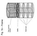
- FIGS. 1A and 1Bare simplified diagrams illustrating a basket apparatus for use in material processing for crystal growth according to an embodiment of the present invention.
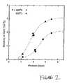
- FIG. 2is a simplified diagram illustrating solubility of GaN plotted against pressure according to an embodiment of the present invention.
- FIG. 3is a simplified diagram of an autoclave with a purge according to an embodiment of the present invention.
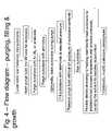
- FIG. 4is a simplified diagram illustrating a crystal growth method according to an embodiment of the present invention.
- FIG. 5is a simplified diagram illustrating a solvent removal and recycling method according to an embodiment of the present invention.
- FIGS. 6A and 6Bare simplified diagrams illustrating a solvent removal and recycle method for crystal growth according to an embodiment of the present invention.
- the present inventionprovides a method for obtaining a gallium-containing nitride crystal by an ammonobasic or ammonoacidic technique, but there can be others.
- the present inventionprovides an apparatus for large scale processing of nitride crystals, but it would be recognized that other crystals and materials can also be processed.
- Such crystals and materialsinclude, but are not limited to, GaN, AlN, InN, InGaN, AlGaN, and AlInGaN, and others for manufacture of bulk or patterned substrates.
- Such bulk or patterned substratescan be used for a variety of applications including optoelectronic devices, lasers, light emitting diodes, solar cells, photoelectrochemical water splitting and hydrogen generation, photodetectors, integrated circuits, and transistors, among other devices.
- Gallium-containing nitridemeans a nitride of gallium and optionally other element(s) of group XIII (according to IUPAC, 1989). It includes, but is not restricted to, the binary compound GaN, ternary compounds such as AlGaN, InGaN and also AlInGaN, where the ratio of the other elements of group XIII to Ga can vary in a wide range.
- Bulk monocrystalline gallium-containing nitridemeans a monocrystalline substrate made of gallium-containing nitride from which optoelectronic devices such as LED or LD can be formed by epitaxial methods such as MOCVD and HVPE.
- Supercritical solventmeans a fluid in a supercritical state. It can also contain other components in addition to the solvent itself as long as these components do not substantially influence or disturb function of supercritical solvent.
- the solventcan contain ions of alkali metals.
- a superheated solventthat is, a solvent heated to a temperature above its boiling point at atmospheric pressure, may also be referred to as supercritical. The latter designation may be useful in cases where the precise critical point of the solvent is not known, due, for example, to the presence of dissolved alkali ions and group III ions, molecules, or complexes.
- Supercritical solutionis used when referring to the supercritical solvent when it contains gallium in a soluble form originating from the etching of gallium-containing feedstock.
- Etching of gallium-containing feedstockmeans a process (either reversible or irreversible) in which said feedstock undergoes a chemical reaction and is taken up to the supercritical solvent as gallium in a soluble form, possibly gallium-complex compounds.
- Crystallizationmeans the reverse process of etching, in which gallium in a soluble form, for example, gallium-complex compounds, undergoes a chemical reaction to form crystalline gallium-containing nitride, preferably as an epitaxial layer on a seed crystal.
- Solubilitymeans the concentration of dissolved gallium in a soluble form, for example, gallium-complex compounds, that is in chemical equilibrium with crystalline gallium-containing nitride at a given temperature, pressure, and mineralizer concentration.
- Processing the feedstockmeans a process whereby gallium in a soluble form is prepared from the feedstock.
- processingmeans etching.
- processingmeans dissolution.
- Gallium-complex compoundsare complex compounds, in which a gallium atom is a coordination center surrounded by ligands, such as NH 3 molecules or its derivatives, like NH 2 ⁇ , NH 2 ⁇ , etc.
- Negative temperature coefficient of solubilitymeans that the solubility of the respective compound is a monotonically decreasing function of temperature if all other parameters are kept constant.
- positive pressure coefficient of solubilitymeans that, if all other parameters are kept constant, the solubility is a monotonically increasing function of pressure.
- Over-saturation of supercritical solution with respect to gallium-containing nitridemeans that the concentration of gallium in a soluble form in said solution is higher than that in chemical equilibrium.
- such an over-saturationcan be achieved by either increasing the temperature and/or decreasing the pressure.
- Spontaneous crystallizationmeans an undesired process where nucleation and growth of the gallium-containing nitride from over-saturated supercritical solution take place at any site within an autoclave except at the surface of a seed crystal where the growth is desired.
- Spontaneous crystallizationalso comprises nucleation and disoriented growth on the surface of seed crystal.
- Selective crystallization on a seedmeans a process of crystallization on a seed carried out without spontaneous crystallization.
- Autoclavemeans a closed container which has a reaction chamber where the ammonobasic or ammonoacidic process according to the present invention is carried out.
- closedis understood to mean sealed and gas tight in the ordinary meaning.
- an autoclaveis understood to be externally heated, that is, so that the temperature of the inner walls of the autoclave is approximately equal to the temperature of the supercritical fluid proximate to the autoclave walls in the ordinary meaning.
- High pressure apparatusmeans an apparatus capable of containing supercritical ammonia and a growth environment for gallium-containing nitride at temperatures between about 100 degrees Celsius and about 800 degrees Celsius and pressures between about 1 kilobar (kbar) and about 10 kbar.
- the high pressure apparatuscomprises an autoclave, as described by U.S. Pat. No. 7,335,262, which is hereby incorporated by reference in its entirety.
- the high pressure apparatusis an internally heated high pressure apparatus, as described in U.S. Pat. No. 7,125,453, and in U.S. Patent Applications 2006/0177362A1 and U.S. Ser. No. 12/133,364, which are hereby incorporated by reference in their entirety.
- the apparatusis described as being vertically oriented.
- the apparatusis instead horizontally oriented or oriented at an oblique angle intermediate between vertical and horizontal, and may be rocked so as to facilitate convection of the supercritical fluid within the high pressure apparatus.
- the present inventioncan provide a gallium-containing nitride monocrystal having a large size and a high quality.
- Such gallium-containing nitride crystalscan have a surface area of more than 2 cm 2 and a dislocation density of less than 10 6 cm ⁇ 2 .
- Gallium-containing nitride crystals having a thickness of at least 200 ⁇ m (preferably at least 500 ⁇ m) and a FWHM of 50 arcsec or lesscan also be obtained.
- the gallium-containing nitride crystalis a crystal of nitride of gallium and optionally other element(s) of Group XIII (the numbering of the Groups is given according to the IUPAC convention of 1989 throughout this application).
- These compoundscan be represented by the formula Al x Gal 1-x-y In y N, wherein 0 ⁇ x ⁇ 1, 0 ⁇ y ⁇ 1, 0 ⁇ x+y ⁇ 1; preferably 0 ⁇ x ⁇ 0.5 and 0 ⁇ y ⁇ 0.5.
- the gallium-containing nitrideis gallium nitride, in a further preferred embodiment part (e.g. up to 50 mol.-%) of the gallium atoms can be replaced by one or more other elements of Group XIII (especially Al and/or In).
- the gallium-containing nitridemay additionally include at least one donor and/or at least one acceptor and/or at least one magnetic dopant to alter the optical, electrical and magnetic properties of the substrate.
- Donor dopants, acceptor dopants and magnetic dopantsare well-known in the art and can be selected according to the desired properties of the substrate.
- the donor dopantsare selected from the group consisting of Si and O.
- acceptor donorsMg and Zn are preferred.
- Any known magnetic dopantcan be included into the substrates of the present invention.
- a preferred magnetic dopantis Mn and possibly also Ni and Cr.
- concentrations of the dopantsare well-known in the art and depend on the desired end application of the nitride. Typically the concentrations of these dopants are ranging from 10 17 to 10 21 cm ⁇ 3 .
- the gallium-containing nitride crystalcan also contain alkali elements, usually in an amount of more than about 0.1 ppm. Generally it is desired to keep the alkali elements content lower than 10 ppm, although it is difficult to specify what concentration of alkali metals in gallium-containing nitride has a disadvantageous influence on its properties.
- halogensare present in the gallium-containing nitride.
- the halogenscan be introduced either intentionally (as a component of the mineralizer) or unintentionally (from impurities of the mineralizer or the feedstock). It is usually desired to keep the halogen content of the gallium-containing nitride crystal in the range of about 0.1 ppm or less.
- the process of the inventionis a supercritical crystallization process, which includes at least two steps: an etching step at a first temperature and at a first pressure and a crystallization step at a second temperature and at a second pressure. Since generally high pressures and/or high temperatures are involved, the process according to the invention is preferably conducted in an autoclave.
- the two stepsi.e. the etching step and the crystallization step
- the processcan be conducted in one reactor but the etching step is conducted before the crystallization step.
- the reactorcan have the conventional construction of one single chamber.
- the process of the invention in the two-step embodimentcan be conducted using constant pressure and two different temperatures or using constant temperature and two different pressures. It is also possible to use two different pressures and two different temperatures.
- the exact values of pressure and temperatureshould be selected depending on the feedstock, the specific nitride to be crystallized and the solvent.
- the pressureis in the range of 1 to 10 kbar, preferably 1 to 5.5 and more preferably 1.5 to 3 kbar.
- the temperatureis in the range of 100 degrees Celsius to 800 degrees Celsius, preferably 300 degrees Celsius to 600 degrees Celsius, more preferably 400 degrees Celsius to 550 degrees Celsius.
- the difference in pressureshould be from 0.1 kbar to 9 kbar, preferably from 0.2 kbar to 3 kbar. However, if the etching and crystallization are controlled by the temperature, the difference in temperature should be at least 1 degree Celsius, and preferably from 5 degrees Celsius to 150 degrees Celsius.
- the etching step and the crystallization stepare conducted at least partially simultaneously in the same container.
- the pressureis practically uniform within the container, while the temperature difference between the etching zone and crystallization zone should be at least 1 degree Celsius, and preferably is from 5 degrees Celsius to 150 degrees Celsius.
- the temperature difference between the etching zone and the crystallization zoneshould be controlled so as to ensure chemical transport in the supercritical solution, which takes place through convection.
- FIG. 1A possible construction of a preferred container is given in FIG. 1 .
- the processwill be explained particularly with respect to this preferred embodiment.
- the inventioncan be conducted with different container constructions as long as the principles outlined in the specification and the claims are adhered to.
- the processcan be conducted in an apparatus comprising an autoclave 1 having an internal space and comprising at least one device 4 , 5 , 6 for heating the autoclave to at least two zones having different temperatures, wherein the autoclave comprises a device which separates the internal space into an etching zone 13 and a crystallization zone 14 . These two zones having different temperatures should preferably coincide with the etching zone 13 and the crystallization zone 14 .
- the device which separates the internal space of the autoclavecan be, for example, at least one baffle 12 having at least one opening 2 . Examples are baffles having a central opening, circumferential openings or a combination thereof.
- the size of the opening(s) 2should be large enough to allow transport between the zones but should be sufficiently small to maintain a temperature gradient in the reactor.
- the appropriate size of the openingdepends on the size and the construction of the reactor and can be easily determined by a person skilled in the art.
- two different heating devicescan be employed, the position of which corresponds to etching zone 13 and the crystallization zone 14 .
- a third cooling means 6is present between the first and the second heating devices and is located at approximately the position of the separating device.
- the cooling means 6can be realized by liquid (e.g. water) cooling or preferably by fan cooling.
- the heating devicesare powered electrically, by either inductive or, preferably, resistive heating means. Use of a heating 4 —cooling 6 —heating 5 configuration gives wider possibilities in forming the desired temperature distribution within the autoclave.
- the apparatusincludes one or more basket devices 19 that are described in more detail below.
- the autoclavemay further comprise a liner or capsule (not shown in FIG. 1 ).
- the liner or capsulemay comprise a precious metal, such as at least one of silver, gold, platinum, palladium, rhodium, iridium, or ruthenium.
- the linermay prevent or inhibit corrosion of the walls of the autoclave and/or contamination of the growing crystals by the components of the autoclave. Examples of suitable liners or capsules are described in Japanese patent application number JP2005289797A2, U.S. Pat. No. 7,125,453, U.S. patent application Ser. No. 12/133,365, and K. Byrappa and M. Yoshimura on pages 94-96 and 152 of Handbook of Hydrothermal Technology (Noyes Publications, Park Ridge, N.J., 2001), each of which is hereby incorporated by reference in their entirety.
- a gallium-containing feedstockan alkali metal-containing component, at least one crystallization seed and a nitrogen-containing solvent are provided in at least one container.
- the gallium-containing feedstockis placed in the etching zone and the at least one crystallization seed is placed in the crystallization zone.
- the alkali metal containing componentis also preferably placed in the etching zone.
- the nitrogen-containing solventis added into the container, which is then closed. Subsequently the nitrogen-containing solvent is brought into a supercritical state, e.g. by pressure and/or heat.
- gallium-containing feedstockany materials containing gallium, which can be etched or dissolved in the supercritical solvent under the conditions of the present invention, can be used as a gallium-containing feedstock.
- the gallium-containing feedstockwill be a substance or mixture of substances, which contains at least gallium, and optionally alkali metals, other Group XIII elements, nitrogen, and/or hydrogen, such as metallic Ga, alloys and inter-metallic compounds, hydrides, amides, imides, amidoimides, azides.
- Suitable gallium-containing feedstockscan be selected from the group consisting of gallium nitride GaN, azides such as Ga(N 3 ) 3 , imides such as Ga 2 (NH) 3 , amido-imides such as Ga(NH)NH 2 , amides such as Ga(NH 2 ) 3 , hydrides such as GaH 3 , gallium-containing alloys, metallic gallium and mixtures thereof.
- Preferred feedstocksare metallic gallium and gallium nitride and mixtures thereof. Most preferably, the feedstock is metallic gallium or gallium nitride.
- Group XIIIis to be incorporated into the gallium-containing nitride crystal, corresponding compounds or mixed compounds including Ga and the other Group XIII element can be used. If the substrate is to contain dopants or other additives, precursors thereof can be added to the feedstock.
- the form of the feedstockis not particularly limited and it can be in the form of one or more pieces or in the form of a powder. If the feedstock is in the form of a powder, care should be taken that individual powder particles are not transported from the etching zone to the crystallization zone, where they can cause irregular crystallization. It is preferable that the feedstock is in one or more pieces and that the surface area of the feedstock is larger than that of the crystallization seed.
- the nitrogen-containing solvent employed in the present inventionshould be able to form a supercritical fluid, in which gallium can be etched in the presence of alkali metal ions.
- the solventis ammonia, a derivative thereof or mixtures thereof.
- An example of a suitable ammonia derivativeis hydrazine.
- the solventis ammonia.
- halogense.g. in the form of halides are preferably not intentionally added into the reactor unless a liner or capsule is present. Although traces of halogens may be introduced into the system in the form of unavoidable impurities of the starting materials, care should be taken to keep the amount of halogen as low as possible.
- a nitrogen-containing solventsuch as ammonia it is not necessary to include nitride compounds into the feedstock.
- Metallic galliumor aluminum or indium can be employed as the source material while the solvent provides the nitrogen required for the nitride formation.
- solubility of gallium-containing feedstocksuch as gallium and corresponding elements of Group XIII and/or their compounds
- a solubilization aidsuch as a solubilization aid
- Lithium, sodium and potassiumare preferred as alkali metals, wherein sodium and potassium are more preferred.
- the mineralizercan be added to the supercritical solvent in elemental form or preferably in the form of its compound. Generally the choice of the mineralizer depends on the solvent employed in the process. Alkali metal having a smaller ion radius can provide lower solubility than that obtained with alkali metals having a larger ion radius.
- the mineralizeris in the form of a compound, it is preferably an alkali metal hydride such as MH, an alkali metal nitride such as M 3 N, an alkali metal amide such as MNH 2 , an alkali metal imide such as M 2 NH or an alkali metal azide such as MN 3 (wherein M is an alkali metal).
- concentration of the mineralizeris not particularly restricted and is selected so as to ensure adequate levels of solubility. It is usually in the range of 1:200 to 1:2, in the terms of the mols of the metal ion based on the mols of the solvent (molar ratio). In a preferred embodiment the concentration is from 1:100 to 1:5, more preferably 1:20 to 1:8 mols of the metal ion based on the mols of the solvent.
- the presence of the alkali metal in the processcan lead to alkali metal elements in the thus prepared substrates. It is possible that the amount of alkali metal elements is more than about 0.1 ppm, even more than 10 ppm. However, in these amounts the alkali metals do not detrimentally effect the properties of the substrates. It has been found that even at an alkali metal content of 500 ppm, the operational parameters of the substrate according to the invention are still satisfactory.
- the mineralizermay comprise an ammonium halide, such as NH 4 F, NH 4 Cl, NH 4 Br, or NH 4 I, a gallium halide, such as GaF 3 , GaCl 3 , GaBr 3 , Ga 3 I, or any compound that may be formed by reaction of one or more of HF, HCl, HBr, HI, Ga, and NH 3 .
- the mineralizermay comprise other alkali, alkaline earth, or ammonium salts, other halides, urea, sulfur or a sulfide salt, or phosphorus or a phosphorus-containing salt.
- a liner or capsulemay be used in conjunction with the autoclave to reduce or eliminate corrosion.
- the mineralizermay be provided as a metal, a loose powder, as granules, or as at least one densified compact or pill.
- the dissolved gallium complexescrystallize in the crystallization step under the low solubility conditions on the crystallization seed(s) which are provided in the container.
- the process of the inventionallows bulk growth of monocrystalline gallium-containing nitride on the crystallization seed(s) and in particular leads to the formation of stoichiometric nitride in the form of a monocrystalline bulk layer on the crystallization seed(s).
- the crystallization seedpreferably comprises a crystalline layer of gallium-containing nitride and optionally one or more other elements of Group XIII.
- the defects surface density of the crystallization seedis preferably less than 10 6 cm ⁇ 2 .
- Suitable crystallization seedsgenerally have a surface area of 8 ⁇ 8 mm 2 or more and thickness of 100 ⁇ m or more, and can be obtained e.g. by HVPE.
- the gallium-containing feedstockis at least partially etched at a first temperature and a first pressure, e.g. in the etching zone of an autoclave.
- Gallium-containing nitridecrystallizes on the crystallization seed (e.g. in the crystallization zone of an autoclave) at a second temperature and at a second pressure while the nitrogen-containing solvent is in the supercritical state, wherein the second temperature is higher than the first temperature and/or the second pressure is lower than the first pressure, in cases of a negative temperature coefficient for solubility.
- the second temperaturemay be lower than the first temperature. If the etching and the crystallization steps take place simultaneously in the same container, the second pressure is essentially equal to the first pressure.
- the solubility under some conditions of the present inventionshows a negative temperature coefficient and a positive pressure coefficient in the presence of alkali metal ions.
- the temperature and pressureare selected such that the gallium-containing feedstock is etched, forming soluble gallium complexes, and the nitrogen-containing solution is undersaturated with respect to gallium-containing nitride.
- the temperature and pressureare selected such that the solution, although it contains approximately the same concentration of gallium complexes as in the etching zone, is over-saturated with respect to gallium-containing nitride.
- gallium-containing nitride on the crystallization seedDue to the temperature gradient, pressure gradient, concentration gradient, different chemical or physical character of dissolved gallium complexes and crystallized product etc., gallium is transported in a soluble form from the etching zone to the crystallization zone. In the present invention this is referred to as chemical transport of gallium-containing nitride in the supercritical solution. It is postulated that the soluble form of gallium is a gallium complex compound, with Ga atom in the coordination center surrounded by ligands, such as NH 3 molecules or its derivatives, like NH 2 ⁇ , NH 2 ⁇ , etc.
- This theorymay be equally applicable for all gallium-containing nitrides, such as AlGaN, InGaN and AlInGaN as well as GaN (the mentioned formulas are only intended to give the components of the nitrides. It is not intended to indicate their relative amounts). In such cases also aluminum and/or indium in a soluble form have to be present in the supercritical solution.
- the gallium-containing feedstockis etched in at least two steps.
- the gallium-containing feedstockgenerally comprises two kinds of starting materials which differ in at least one of the kinetics or thermodynamics of etching. A difference in solubility can be achieved chemically (e.g. by selecting two different chemical compounds) or different etching kinetics can be achieved physically (e.g. by selecting two forms of the same compound having definitely different surface areas, like microcrystalline powder and big crystals).
- the gallium-containing feedstockcomprises two different chemical compounds such as metallic gallium and gallium nitride which etch at different rates.
- the first component of the gallium-containing feedstockis substantially completely etched away at an etching temperature and at an etching pressure in the etching zone.
- the etching temperature and the etching pressurewhich can be set only in the etching zone or preferably in the whole container, are selected so that the second component of the gallium-containing feedstock and the crystallization seed(s) remain substantially unetched.
- This first etching stepresults in an undersaturated or at most saturated solution with respect to gallium-containing nitride.
- the etching temperaturecan be 100 degrees Celsius to 350 degrees Celsius, preferably from 150 degrees Celsius to 300 degrees Celsius.
- the etching pressurecan be 0.1 kbar to 5 kbar, preferably from 0.1 kbar to 3 kbar. Generally the etching temperature is lower than the first temperature.
- the conditions in the crystallization zoneare set at a second temperature and at a second pressure so that over-saturation with respect to gallium-containing nitride is obtained and crystallization of gallium-containing nitride occurs on the at least one crystallization seed.
- the conditions in the etching zoneare set at a first temperature and at a first pressure (practically equal to the second pressure) so that the second component of the gallium-containing feedstock is now etched (second etching step).
- the second temperatureis higher than the first temperature (in the case of a negative temperature coefficient of solubility) and/or the second pressure is lower than the first pressure so that the crystallization can take advantage of the negative temperature coefficient of solubility and/or by means of the positive pressure coefficient of solubility.
- the first temperatureis also higher than the etching temperature.
- Typical pressures for the crystallization step and the second etching stepare in the range of 1 to 10 kbar, preferably 1 to 5.5 and more preferably 1.5 to 3 kbar.
- the temperatureis in the range of 100 to 800 degrees Celsius, preferably 300 to 600 degrees Celsius, more preferably 400 to 550 degrees Celsius.
- the difference in temperatureshould be at least 1 degrees Celsius, and preferably from 5 degrees Celsius to 150 degrees Celsius.
- the temperature difference between the etching zone and crystallization zoneshould be controlled so as to ensure a chemical transport in the supercritical solution, which takes place through convection in an autoclave.
- the crystallizationshould take place selectively on the crystallization seed and not on a wall of the container. Therefore, the over-saturation extent with respect to the gallium-containing nitride in the supercritical solution in the crystallization zone should be controlled so as to be below the spontaneous crystallization level where crystallization takes place on a wall of the autoclave as well as on the seed, i.e. the level at which spontaneous crystallization occurs. This can be achieved by adjusting the chemical transport rate and the crystallization temperature and/or pressure.
- the chemical transportis related on the speed of a convection flow from the etching zone to the crystallization zone, which can be controlled by the temperature difference between the etching zone and the crystallization zone, the size of the opening(s) of baffle(s) between the etching zone and the crystallization zone and so on.
- feedstock materialcan also be prepared using a method similar to those described above. The method involves:
- Gallium-containing nitrideexhibits good apparent solubility in supercritical nitrogen-containing solvents (e.g. ammonia), provided alkali metals or their compounds, such as KNH 2 , are introduced into it.
- FIG. 2shows the solubility of gallium-containing nitride in a supercritical solvent versus pressure for temperatures of 400 and 500 degrees Celsius wherein the solubility is defined by the molar percentage: S m ⁇ GaN solvent :(KNH 2 +NH 3 ) 100%.
- the solventis the KNH 2 solution in supercritical ammonia of a molar ratio x ⁇ KNH 2 :NH 3 equal to 0.07.
- S mshould be a smooth function of only three parameters: temperature, pressure, and molar ratio of mineralizer (i.e. S m ⁇ S m (T, p, x)).
- Small changes of S mcan be expressed as: ⁇ S m ⁇ ( ⁇ S m / ⁇ T)
- the partial differentialsare called “coefficients” (e.g. ( ⁇ S m / ⁇ T)
- the diagram shownillustrates that the solubility increases with pressure and decreases with temperature in the presence of alkali-containing mineralizer, which means that it possesses a negative temperature coefficient and a positive pressure coefficient.
- alkali-containing mineralizerwhich means that it possesses a negative temperature coefficient and a positive pressure coefficient.
- Such featuresallow obtaining a bulk monocrystalline gallium-containing nitride by etching in the higher solubility conditions, and crystallization in the lower solubility conditions.
- the negative temperature coefficientmeans that, in the presence of temperature gradient, the chemical transport of gallium in a soluble form can take place from the etching zone having a lower temperature to the crystallization zone having a higher temperature.
- the process according to inventionallows the growth of bulk monocrystalline gallium-containing nitride on the seed and leads in particular to creation of stoichiometric gallium nitride, obtained in the form of monocrystalline bulk layer grown on a gallium-nitride seed. Since such a monocrystal is obtained in a supercritical solution that contains ions of alkali metals, it contains also alkali metals in a quantity higher than 0.1 ppm. Because it is desired to maintain a purely basic character of a supercritical solution, mainly in order to avoid corrosion of the apparatus, halides are preferably not intentionally introduced into the solvent.
- the process of the inventioncan also provide a bulk monocrystalline gallium nitride in which part of the gallium, e.g.
- the bulk monocrystalline gallium nitridemay be doped with donor and/or acceptor and/or magnetic dopants. These dopants can modify optical, electric and magnetic properties of a gallium-containing nitride.
- the bulk monocrystalline gallium nitridecan have a dislocation density below 10 6 cm ⁇ 2 , preferably below 10 5 cm ⁇ 2 , or most preferably below 10 4 cm ⁇ 2 .
- the FWHM of the X-ray rocking curve from (0002) planecan be below 600 arcsec, preferably below 300 arcsec, and most preferably below 60 arcsec.
- the best bulk monocrystalline gallium nitride obtainedmay have a dislocation density lower than 10 4 cm ⁇ 2 and simultaneously a FWHM of X-ray rocking curve from (0002) plane below 60 arcsec.
- the obtained gallium-containing nitride crystals obtained in the present inventionmay be used as a substrate material for optoelectronic semiconductor devices based on nitrides, in particular for laser diodes and light emitting diodes.
- FIGS. 1A and 1Ba schematic of a frame for seed crystals and raw material is shown in by FIGS. 1A and 1B .
- the frameenables seed crystals and raw material to be loaded into a suitable configuration for crystal growth prior to placement inside the high pressure apparatus and in a form that is convenient for subsequent handling.
- the frameshould retain good rigidity under crystal growth conditions and be chemically inert to the crystal growth environment, neither contributing contamination to the growing crystals nor undergoing significant corrosion.
- the materials of construction of the frame and the components thereofmay include one or more of copper, copper-based alloy, gold, gold-based alloy, silver, silver-based alloy, palladium, platinum, iridium, ruthenium, rhodium, osmium, titanium, vanadium, chromium, iron, iron-based alloy, nickel, nickel-based alloy, zirconium, niobium, molybdenum, tantalum, tungsten, rhenium, silica, alumina, combinations thereof, and the like.
- Iron-base alloys that may be used to form the frameinclude, but are not limited to, stainless steels.
- Nickel-base alloys that may be used to form the frameinclude, but are not limited to, inconel, hastelloy, and the like. Again, there can be other variations, modifications, and alternatives.
- the components of the frameare fabricated from an alloy comprising at least two elements, for increased hardness and creep resistance.
- the frame and its componentsmay comprise wire, wire cloth or mesh, foil, plate, sheet, square bar, round bar, rectangular bar, tubing, threaded rod, and fasteners.
- the frame and its componentsmay be attached by means of welding, arc welding, resistance welding, brazing, clamping, attachment by means of fasteners such as at least one of screws, bolts, threaded rod, and nuts, and the like.
- the framemay include, as components, a baffle, a raw material basket, and a rack for suspending seed crystals, plus a means for attaching at least two of the aforementioned components.
- a bafflefor suspending seed crystals
- a rackfor suspending seed crystals, plus a means for attaching at least two of the aforementioned components.
- the basketis positioned below the baffle and the seed rack is positioned above the baffle.
- FIG. 1Aappropriate for the case where the crystal to be grown has a solubility that increases with increasing temperature (i.e., a positive temperature coefficient of solubility)
- the basketis positioned above the baffle and the seed rack is positioned below the baffle. Growth of gallium nitride crystals under ammonobasic conditions normally falls in this category.
- a larger volumemay be provided for the crystal growing region, that is, the region containing the seed rack, than for the nutrient region, that is, the region containing the basket.
- the ratio of the volumes of the crystal growing region and the nutrient regionis between 1 and 5. In other embodiments, this ratio is between 1.25 and 3, or between 1.5 and 2.5.
- the overall diameter and height of the frameare chosen for a close fit within the high pressure apparatus, so as to maximize the utilization of the available volume and optimize the fluid dynamics.
- the diameter of the framemay be between 1 inch and 2 inches, between 2 inches and 3 inches, between 3 inches and 4 inches, between 4 inches and 6 inches, between 6 inches and 8 inches, between 8 inches and 10 inches, between 10 inches and 12 inches, between 12 inches and 16 inches, between 16 inches and 24 inches, or greater than 24 inches.
- the ratio of the overall height of the frame to its diametermay be between 1 and 2, between 2 and 4, between 4 and 6, between 6 and 8, between 8 and 10, between 10 and 12, between 12 and 15, between 15 and 20, or greater than 20.
- the baffleprovides a means for dividing the high pressure apparatus into which the frame is to be inserted into two separate regions, and comprises one or more disks.
- the two regionsare in fluid communication with each other, as baffle has a plurality of through-holes, or openings.
- a fraction of the cross-sectional area of the baffleis open.
- bafflehas a fractional open area of between about 0.5% and about 30%, but can also have other percentages.
- the bafflehas a fraction open area between 2% and 20%, or between 5% and 15%.
- Baffleserves the purpose of confining the at least one (or more) raw material to a specific region or end of chamber while permitting solvent and, under high pressure high temperature (HPHT) conditions, supercritical fluid, to migrate throughout the high pressure apparatus by passing freely through through-holes in baffle. Often times, this feature is particularly useful in applications such as crystal growth, in which the supercritical fluid transports the at least one material, a nutrient material, from one region of the chamber, defined by placement of baffle, to another region where crystal growth on seed crystals take place.
- the diameter of the baffleis equal to the maximum diameter of the overall frame. In other embodiments, the diameter of the baffle is slightly less than the maximum diameter of the overall frame, providing an annular space through which fluid can flow under crystal growth conditions.
- the diameter of the bafflemay be less than the maximum diameter of the overall frame by 0.5 inch or less.
- the openings in the baffleshould be large enough so as not to clog readily.
- the diameters of the openings in the baffleare between 0.020 inch and 0.5 inch.
- the diameters of the openings in the baffleare between 0.050 inch and 0.25 inch.
- the bafflecomprises a single disk with a thickness between 0.020 inch and 0.5 inch.
- the bafflecomprises a single disk with a thickness between 0.050 inch and 0.25 inch.
- the bafflecomprises two disks, three disks, or more.
- one or more of the openings in the diskslie above one another. In other multi-disk embodiments, one or more of the openings in the disks do not lie above one another.
- the effective fractional open area in multi-disk baffle embodimentsmay therefore lie between the fractional open area of each disk, as an upper bound, and the product of the fractional open areas of each disk.
- the raw material basketprovides a convenient means for transferring the raw material into the high pressure apparatus, for permitting facile fluid communication from the region between raw material particles within the basket and the crystal growth region, and for removing un-consumed raw material from the reactor at the conclusion of a growth run.
- the basketcomprises wire mesh or wire cloth, as indicated schematically in the figures.
- the diameter of the wire in the mesh or clothmay be between 0.001 inch and 0.25 inch, between 0.005 inch and 0.125 inch, or between 0.010 inch and 0.080 inch.
- the wire mesh or wire clothmay be contained within and, optionally, attached to a frame comprising larger-diameter wire so as to provide improved mechanical support.
- the basketcomprises foil or plate with a plurality of through-holes or openings.
- the size of the openings in the wire mesh, wire cloth, or foil or plateshould be small enough so that raw material particles do not pass through them during crystal growth, even after a significant portion of the raw material has been etched away and/or consumed by the crystal growth operation.
- the openings in the wire mesh, wire cloth, or foil or platehave a diameter between 0.005 inch and 0.5 inch. In other embodiments, the openings have a diameter between 0.010 inch and 0.125 inch, or between 0.025 inch and 0.080 inch.
- hollow pipes, with openings that are covered by wire meshare placed within the basket prior to loading of the raw material so as to improve fluid communication between the region between raw material particles within the basket and the crystal growth region. Suitable configurations for such hollow pipes are described by U.S. Pat. No. 3,245,760, which is hereby incorporated by reference in its entirety, according to a specific embodiment.
- the raw materialis placed in the basket prior to placement of seed crystals on the seed rack, so as to minimize the likelihood of breakage of the latter.
- the raw materialmay be supplied in various forms.
- the raw materialcomprises single crystals or chunks or grit of polycrystalline material.
- the raw materialcomprises chunks of sintered polycrystalline material.
- the raw materialmay be derived from by-product single- or poly-crystalline GaN deposited on the wall or miscellaneous surfaces with a hydride vapor phase epitaxy (HVPE) reactor.
- HVPEhydride vapor phase epitaxy
- the raw materialcomprises plates of single- or poly-crystalline GaN grown on a substrate by HVPE.
- the raw materialis derived from sintered GaN powder, as described by U.S. Pat. No. 6,861,130, which is hereby incorporated by reference in its entirety.
- the raw materialis derived from polycrystalline GaN plates comprising a columnar microstructure, as described by U.S. Patent Application 2007/0142204A1, which is hereby incorporated by reference in its entirety.
- the raw materialmay contain oxygen at a concentration below 10 19 cm ⁇ 3 , below 10 18 cm ⁇ 3 , or below 10 17 cm ⁇ 3 .
- the raw materialmay contain an n-type dopant, such as Si or O, a p-type dopant, such as Mg or Zn, a compensatory dopant, such as Fe or Co, or a magnetic dopant, such as Fe, Ni, Co, or Mn, at concentrations between 10 16 cm ⁇ 3 and 10 21 cm ⁇ 3 .
- the particle size distribution of the raw materiallies between about 0.020 inch and about 5 inches. In another embodiment, the particle size distribution of the raw material lies between about 0.050 inch and about 0.5 inch.
- the total surface area of the raw materialis greater, by at least a factor of three, than the total surface area of all the seed crystals that are placed in the seed rack.
- the raw materialcomprises a metal that will become molten at elevated temperatures, for example, gallium, indium, sodium, potassium, or lithium. If placed in direct contact with the inner surface of the autoclave or capsule the metal may form an alloy, compromising the integrity of the autoclave or capsule.
- at least one crucible containing at least one metalis placed within or proximate to the raw material basket.
- the crucibleshould be chemically inert with respect to the supercritical fluid crystal growth environment and should not react or alloy with the at least one metal.
- the cruciblecomprises molybdenum, tantalum, niobium, iridium, platinum, palladium, gold, silver, or tungsten.
- the cruciblecomprises alumina, magnesia, calcia, zirconia, yttria, aluminum nitride or gallium nitride.
- the cruciblemay comprise a sintered or other polycrystalline material.
- the seed rackprovides a convenient means for transferring the seed crystals or plates into the high pressure apparatus, for permitting facile fluid communication between the seed crystals or plates and the nutrient region on the other side of the baffle, and for removing the grown crystals from the reactor at the conclusion of a growth run.
- the seed rackshould be easy to load and unload, enable efficient usage of the available crystal growth volume, and minimize breakage and other yield losses of the crystals.
- the seed crystals or platescomprise gallium nitride.
- the seed crystals or platesmay comprise aluminum nitride, sapphire, silicon carbide, MgAl 2 O 4 spinel, zinc oxide, or the like.
- the framefurther comprises a set of stacked disks or baffles on the top end of the frame.
- the stacked disks or bafflesreduce convective heat transfer from the supercritical fluid during crystal growth to the upper end of the autoclave so that the seal of the autoclave may be at a reduced temperature relative to the upper end of the interior of the autoclave.
- one or more disks or bafflesare placed on top of the frame after insertion of the latter into a high pressure apparatus.
- the frameAfter loading the frame with seed crystals and raw material, the frame is placed inside a high pressure apparatus or in a liner or capsule which is then placed inside a high pressure apparatus.
- At least one mineralizermay be added.
- the mineralizermay comprise an alkali metal such as Li, Na, K, Rb, or Cs, an alkaline earth metal, such as Mg, Ca, Sr, or Ba, or an alkali or alkaline earth hydride, amide, imide, amido-imide, nitride, or azide.
- the mineralizermay comprise other alkali, alkaline earth, or ammonium salts, urea, sulfur or a sulfide salt, or phosphorus or a phosphorus-containing salt.
- the mineralizermay be provided as a loose powder, as granules, or as at least one densified compact or pill.
- the mineralizermay be added to the raw material basket, may be placed in a crucible, or may be placed directly in the high pressure apparatus or capsule. In a preferred embodiment, the mineralizer is added to the high pressure apparatus or capsule in the absence of exposure to air, such as inside a glove box.
- a gettermay also be added to the reaction mix.
- the getterpreferentially reacts with residual or adventitious oxygen or moisture present, improving the purity and transparency of the grown GaN crystals.
- the gettermay comprise at least one of an alkaline earth metal, Sc, Ti, V, Cr, Y, Zr, Nb, Hf, Ta, W, a rare earth metal, and their nitrides, amides, imides, amido-imides, or halides.
- At least one of the mineralizer and the getterare placed in crucibles within or proximate to the raw material basket.
- metallic precursors for the raw material, mineralizer, and/or getteris convenient in some respects.
- the metalis typically available commercially in high purity, and no further synthesis is required.
- the use of a pure metalmay generate undesirable gases, such as hydrogen.
- the metals listed belowwill undergo one or more of the following reactions: Ga+NH 3 ⁇ GaN+ 3/2H 2 Na+NH 3 ⁇ NaNH 2 +1 ⁇ 2H 2 K+NH 3 ⁇ KNH 2 +1 ⁇ 2H 2 Mg+2NH 3 ⁇ Mg(NH 2 ) 2 +H 2 3Mg+2NH 3 ⁇ Mg 3 N 2 +3H 2 Y+3NH 3 ⁇ Y(NH 2 ) 3 + 3/2H 2 Y+NH 3 ⁇ YN+ 3/2H 2
- the presence of hydrogen in the supercritical fluid solventmay decrease the solubility of gallium-containing species and, further, may embrittle the metal constituting the autoclave walls.
- azidesas mineralizers is convenient in that they are often available commercially in high purity, can be purified further, and are considerably less hygroscopic than the alkali metals or amides or the alkaline earth nitrides, for example.
- Use of azide mineralizersis suggested by Dwili ⁇ ski in U.S. Pat. No. 7,364,619, which is hereby incorporated by reference in its entirety.
- these two effectsare combined so as to cancel each other out.
- Metalsincluding raw materials, mineralizers, and getters, are added together with azide mineralizer precursors such that H 2 and N 2 are generated in approximately a 3:1 ratio.
- the reaction containerfurther comprises means for catalyzing NH 3 formation from H 2 and N 2 .
- Catalysis of the reaction between H 2 and N 2 liberated in the reaction of the metal with ammonia and decomposition of the azide, respectively, to re-form ammoniamay be performed by the autoclave walls or by added catalyst.
- the added catalystmay comprise powder, granules, foil, a coating, bulk material, or a porous pellet.
- the added catalystmay comprise at least one of iron, cobalt, nickel, titanium, molybdenum, tungsten, aluminum, potassium, cesium, calcium, magnesium, barium, zirconium, osmium, uranium or a lanthanide, ruthenium, platinum, palladium, or rhodium.
- a mole of added NaN 3will generate 4/3 mole of N 2 .
- the high pressure apparatusis then closed and sealed except for a connection to a gas, liquid, or vacuum manifold.
- the high pressure apparatuscomprises an autoclave, as described by U.S. Pat. No. 7,335,262, which is hereby incorporated by reference in its entirety.
- the inner diameter of the autoclavemay be between 1 inch and 2 inches, between 2 inches and 3 inches, between 3 inches and 4 inches, between 4 inches and 6 inches, between 6 inches and 8 inches, between 8 inches, and 10 inches, between 10 inches and 12 inches, between 12 inches and 16 inches, between 16 inches and 24 inches, or greater than 24 inches.
- the clearance between the inner diameter of the autoclave and the outer diameter of the framemay be between 0.005 inch and 1 inch, or between 0.010 inch and 0.25 inch.
- the ratio of the inner height of the autoclave to its inner diametermay be between 1 and 2, between 2 and 4, between 4 and 6, between 6 and 8, between 8 and 10, between 10 and 12, between 12 and 15, between 15 and 20, or greater than 20.
- the ratio of the inner height of the autoclave to its inner diametermay be between 1 and 2, between 2 and 4, between 4 and 6, between 6 and 8, between 8 and 10, between 10 and 12, between 12 and 15, between 15 and 20, or greater than 20.
- the high pressure apparatusis evacuated, so as to remove air, moisture, and other volatile contaminants.
- the high pressure apparatusis heated during evacuation, to a temperature between about 25 degrees Celsius and about 500 degrees Celsius.
- the high pressure heater apparatusis heated using the same heating elements that are used during high pressure processing.
- the high pressure apparatusis subjected to at least two cycles of evacuation followed by back-filling with an inert gas such as argon or nitrogen.
- a limitation of evacuation as a means for removing air, moisture, and other volatile components from the autoclaveis the rather limited conductance of the vacuum connection, which may require long or very long evacuation times.
- the conductance of a long tubeis proportional to the diameter cubed divided by the length.
- the inner diameter of the vacuum connectionmight be about 2 millimeters over a length of about 50 millimeters.
- airsuch a connection will have a conductance of approximately 0.02 liters per second.
- the corresponding time constant for evacuationwill be approximately 5000 seconds (1.4 hour).
- the pressurewill decay by a factor of e (2.718) during each time constant. Removal of 99.999% of the starting gases requires approximately 11.5 time constants, or 16 hours in this example. Removal of noncondensible gases, such as water vapor, can take even longer, due to adsorption of water on the walls of the apparatus and, especially, on high surface area material inside the autoclave, such as porous polycrystalline GaN raw material. Removal of condensable gases from the autoclave can be accelerated by heating during evacuation. In one specific embodiment, the autoclave is heated to a temperature between about 25 degrees Celsius and about 500 degrees Celsius while being evacuated.
- the high pressure apparatus containing the filled frameis purged to remove air, moisture, and other volatile contaminants, as shown in FIG. 3 .
- a method of processing materials in a high pressure apparatusis shown by FIGS. 4 and 5 , which are provided for referencing purposes to describe the processes herein.
- Purgingmay provide for superior removal of air, moisture, and other volatile contaminants, relative to evacuation, because of the limited conductance through a tube or long hole to the interior of the autoclave or capsule.
- the efficiency of purgingmay be enhanced by causing purge gas to flow from one end of the interior volume of the autoclave to the other.
- the autoclaveis coupled to a gas source by means of at least one fill tube or purge tube, preferably without exposing the contents of the autoclave to air according to a specific embodiment.
- the gas sourcemay comprise at least one of nitrogen, argon, hydrogen, helium, and solvent vapor, among others.
- both a first fill or purge tube and a second fill or purge tubeare coupled to a gas source and/or exhaust.
- the autoclavecomprises a double-ended autoclave, with plugs at each and purge connections on each plug.
- an inner purge tubeis placed inside the fill or outer purge tube and positioned so that one end is proximate to the bottom end of the autoclave.
- the inner purge tube and outer purge tubemay be fabricated from at least one of copper, copper-based alloy, gold, gold-based alloy, silver, silver-based alloy, palladium, platinum, iridium, ruthenium, rhodium, osmium, iron, iron-based alloy, nickel, nickel-based alloy, molybdenum, and combinations thereof.
- Iron-base alloysthat may be used to form the inner purge tube or outer purge tube include, but are not limited to, stainless steels.
- Nickel-base alloys that may be used to form the inner purge tube or outer purge tubeinclude, but are not limited to, inconel, hastelloy, and the like.
- the outer diameter of the inner purge tubemay be less than the inner diameter of the fill or outer purge tube by at least 0.010 inch, as shown.
- the inner purge tubemay be coupled to the fill or outer purge tube by means of a tee fitting or other suitable technique, so that purge gas introduced through the inner purge tube will exit near the bottom end of the autoclave or capsule, pass through the length of the autoclave before exhausting though the annular space in the fill or outer purge tube outside the inner purge tube and the tee fitting, providing for efficient removal of gas phase contaminants according to a specific embodiment.
- the interface between the tee fitting and the inner purge tubemay be a sliding seal, for example, an O-ring or a differentially-pumped set of Teflon seals or O-rings.
- the rate of flow of the purge gasmay be in the range between 0.05 and 10 standard liters per minute.
- the autoclavemay be heated, for example, to a temperature between 25 degrees Celsius and 500 degrees Celsius during the purge operation, in order to more efficiently remove water and other adsorbed contaminants.
- solvent vaporfor example, gas phase ammonia, may be flowed through the autoclave or capsule in order to remove most or all of the purge gas.
- the inlet of the gas flowfor example, the second fill tube or the purge tube (cf. FIG. 3 ) is then coupled to a source of liquid solvent.
- the autoclave and fill tube(s)may be cooled, or the liquid solvent delivery system and transfer lines heated, so that the former are cooler by between one and 50 degrees Celsius than the latter.
- Liquid solventis then introduced into the autoclave at a rate between 0.1 and 1000 grams per minute.
- the vapor pressure of ammoniais approximately 10 atmospheres.
- the system pressure during solvent deliverymay be above 7 atmospheres, above 8 atmospheres, above 9 atmospheres, or above 10 atmospheres.
- the purge exhaustis closed and the solvent vapor above the liquid is forced to condense into liquid during the filling operation.
- the autoclavemay be actively cooled in order to dissipate the heat released by condensation of the solvent vapor.
- the purge exhaustis fitted with a check valve so that residual purge gas or solvent vapor is allowed to exit when the pressure exceeds a predetermined threshold, but air or other gases are not allowed to flow backward into the autoclave.
- the quantity of solvent in the autoclavemay be determined by using a liquid delivery system with the capability for accurately monitoring and controlling the mass of liquid delivered.
- the amount of ammonia delivered to the autoclaveis quantified by the loss in weight of at least one ammonia supply cylinder. If solvent gas is allowed to exhaust during liquid filling, in the case where ammonia is the solvent, the quantity of vented solvent may be determined by trapping it in aqueous solution and measuring the change in pH and this quantity subtracted from the total liquid delivered to determine the quantity of liquid in the capsule. An analogous method for determining the quantity of vented solvent may be performed in cases where the solvent is different from ammonia.
- the solventis delivered to the autoclave as a vapor at elevated pressure.
- the inlet of the gas flowfor example, the second fill tube or the purge tube (cf. FIG. 3 ) is then coupled to a source of vapor-phase solvent.
- the autoclave and fill tube(s)may be cooled, or the solvent delivery system and transfer lines heated, so that the former are cooler by between one and 50 degrees Celsius than the latter.
- Vapor-phase solventis then introduced into the autoclave at a rate between 0.1 and 1000 grams per minute and allowed to condense in the autoclave.
- the pressure of the solvent vaporshould be higher than the equilibrium vapor pressure at the temperature of the autoclave.
- the pressure during solvent deliverymay be above 7 atmospheres, above 8 atmospheres, above 9 atmospheres, or above 10 atmospheres.
- the purge exhaustis closed and the solvent vapor above the liquid is forced to condense into liquid during the filling operation.
- the autoclavemay be actively cooled in order to dissipate the heat released by condensation of the solvent vapor.
- the purge exhaustis fitted with a check valve so that residual purge gas or solvent vapor is allowed to exit when the pressure exceeds a predetermined threshold, but air or other gases are not allowed to flow backward into the autoclave.
- the quantity of solvent in the autoclavemay be determined by using a vapor delivery system equipped with a mass flow meter.
- the amount of ammonia delivered to the autoclaveis quantified by the loss in weight of at least one ammonia supply cylinder. If solvent gas is allowed to exhaust during liquid filling, in the case where ammonia is the solvent, the quantity of vented solvent may be determined by trapping it in aqueous solution and measuring the change in pH and this quantity subtracted from the total liquid delivered to determine the quantity of liquid in the capsule. An analogous method for determining the quantity of vented solvent may be performed in cases where the solvent is different from ammonia.
- the inner purge tubemay be removed.
- the inner purge tubeis removed after the purging step but before the filling step.
- a gate valve to the autoclaveis then sealed. Once sealed, the interior of the autoclave is substantially air-free, and the at least one material contained therein can be processed with reduced risk of contamination.
- the autoclaveis then heated to crystal growth conditions.
- the thermal cycleincludes a pre-reaction segment to form mineralizer, polycrystalline gallium nitride, dissolved gallium containing complexes, or the like.
- the atmosphere in the autoclavemay be modified during the run. For example, excess H 2 formed by reaction of gallium metal with ammonia may be bled off through the gate valve or allowed to diffuse through a heated palladium membrane. The use of a commercially-available heated palladium membrane offers the convenience of continuous hydrogen removal, without interrupting or perturbing the process, with little or no opportunity for contamination of the process. Excess nitrogen formed by decomposition of an azide mineralizer may be bled off through the gate valve. Additional ammonia may be added to replenish the solvent in the high pressure apparatus.
- the autoclaveAfter performing crystal growth for a predetermined period of time, the autoclave is cooled. When the autoclave has cooled to below 100 degrees Celsius, below 75 degrees Celsius, below 50 degrees Celsius, or below 35 degrees Celsius, a valve to the autoclave is opened and the ammonia is removed.
- gas-phase ammoniais allowed to exit the autoclave and is bubbled through an acidic aqueous solution in order to be chemically trapped.
- gas phase ammoniais passed through a flame so as to burn the ammonia, forming H 2 O and N 2 .
- the ammoniais trapped for recycling and reuse.
- the ammoniamay be removed as either a liquid or a gas.
- the inner purge tube(see FIG. 3 ) is re-inserted into the outer purge or fill tube and the outlet of the inner purge tube connected to the Receiving/Purification tank. Keeping the purge gas exhaust connection (see FIG. 3 ) closed, a valve in the line to the inner purge tube is opened, allowing liquid ammonia to flow through the inner purge tube in the autoclave into the Receiving/Purification tank, which is otherwise closed.
- the Receiving/Purification tankmay be cooled, for example, by chilled water, and/or the autoclave and transfer line may be heated during the ammonia transfer operation, so as to maintain a higher vapor pressure of ammonia in the autoclave as compared to the vapor pressure in the Receiving/Purification tank.
- the temperature differential between the autoclave and the Receiving/Purification tankmay be held between one and 50 degrees Celsius.
- the ammoniais removed as a vapor.
- the outlet of the autoclaveis connected to a condenser above the Receiving/Purification tank and a valve opened.
- Gas-phase ammoniaenters the condenser and condenses into liquid in a heat-exchanger, for example, a chilled-water-cooled coil, at a pressure between about 100 and 250 pounds per square inch.
- the autoclave and transfer linemay be heated to a temperature that is higher than the condenser by between one and 50 degrees Celsius. Residual gases, for example, N 2 and H 2 , may be released by venting to a scrubber and/or a flame.
- the ammoniamay be removed as a liquid.
- a port on the bottom end of the autoclaveis connected to the Receiving/Purification tank and a valve opened, allowing liquid ammonia to flow into the Receiving/Purification tank, which is otherwise closed.
- the Receiving/Purification tankmay be cooled, for example, by chilled water, and/or the autoclave and transfer line may be heated during the ammonia transfer operation, so as to maintain a higher vapor pressure of ammonia in the autoclave as compared to the vapor pressure in the Receiving/Purification tank.
- the temperature differential between the autoclave and the Receiving/Purification tankmay be held between one and 50 degrees Celsius.
- a purifying agentfor example, sodium metal
- the sodiumwill react with residual oxygen and/or water in the ammonia, restoring a very high degree of purity.
- the ammoniamay be transferred to a delivery tank.
- the transferis performed through the gas phase, via a condenser, so as to leave the purifying agent in the receiving/purification tank.
- Liquid ammoniamay be delivered from the delivery tank, via a dip tube, to the autoclave for the next crystal growth run.
- vapor-phase ammoniamay be delivered from the delivery tank to the autoclave for the next crystal growth run.
- the autoclaveAfter removing the ammonia, the autoclave is opened and grown crystals and remaining raw material removed.
- the crystalsmay be sliced in a predetermined orientation to form at least one wafer. After slicing, the crystal wafers may be lapped, polished, and chemical-mechanically polished by methods that are known in the art.
- any of the above sequence of stepsprovides a method according to an embodiment of the present invention.
- the present inventionprovides a method and resulting crystalline material provided by an autoclave apparatus having means for filling with a solvent at elevated pressure.
- stepsare added, one or more steps are removed, or one or more steps are provided in a different sequence without departing from the scope of the claims herein.
- the present method and systemuses a pressure of about 7 atmospheres and greater, but other suitable pressures or specific pressures may exist. In one or more embodiment, the pressure may be slightly higher or lower depending upon the application. Therefore, the above description and illustrations should not be taken as limiting the scope of the present invention which is defined by the appended claims.
Landscapes
- Chemical & Material Sciences (AREA)
- Organic Chemistry (AREA)
- Engineering & Computer Science (AREA)
- Crystallography & Structural Chemistry (AREA)
- Materials Engineering (AREA)
- Metallurgy (AREA)
- Chemical Kinetics & Catalysis (AREA)
- Inorganic Chemistry (AREA)
- Crystals, And After-Treatments Of Crystals (AREA)
Abstract
Description
4. subsequently setting the conditions in the container at a second temperature and at a second pressure so that over-saturation with respect to gallium-containing nitride is obtained and crystallization of gallium-containing nitride occurs on the at least one crystallization seed.
5. perform other steps, as desired.
Ga+NH3═GaN+ 3/2H2
Na+NH3═NaNH2+½H2
K+NH3═KNH2+½H2
Mg+2NH3═Mg(NH2)2+H2
3Mg+2NH3═Mg3N2+3H2
Y+3NH3═Y(NH2)3+ 3/2H2
Y+NH3═YN+ 3/2H2
3NaN3+2NH3=3NaNH2+4N2
Claims (20)
Priority Applications (2)
| Application Number | Priority Date | Filing Date | Title |
|---|---|---|---|
| US12/534,857US8021481B2 (en) | 2008-08-07 | 2009-08-04 | Process and apparatus for large-scale manufacturing of bulk monocrystalline gallium-containing nitride |
| US13/226,249US8444765B2 (en) | 2008-08-07 | 2011-09-06 | Process and apparatus for large-scale manufacturing of bulk monocrystalline gallium-containing nitride |
Applications Claiming Priority (2)
| Application Number | Priority Date | Filing Date | Title |
|---|---|---|---|
| US8680108P | 2008-08-07 | 2008-08-07 | |
| US12/534,857US8021481B2 (en) | 2008-08-07 | 2009-08-04 | Process and apparatus for large-scale manufacturing of bulk monocrystalline gallium-containing nitride |
Related Child Applications (1)
| Application Number | Title | Priority Date | Filing Date |
|---|---|---|---|
| US13/226,249ContinuationUS8444765B2 (en) | 2008-08-07 | 2011-09-06 | Process and apparatus for large-scale manufacturing of bulk monocrystalline gallium-containing nitride |
Publications (2)
| Publication Number | Publication Date |
|---|---|
| US20100031876A1 US20100031876A1 (en) | 2010-02-11 |
| US8021481B2true US8021481B2 (en) | 2011-09-20 |
Family
ID=41651736
Family Applications (2)
| Application Number | Title | Priority Date | Filing Date |
|---|---|---|---|
| US12/534,857ActiveUS8021481B2 (en) | 2008-08-07 | 2009-08-04 | Process and apparatus for large-scale manufacturing of bulk monocrystalline gallium-containing nitride |
| US13/226,249ActiveUS8444765B2 (en) | 2008-08-07 | 2011-09-06 | Process and apparatus for large-scale manufacturing of bulk monocrystalline gallium-containing nitride |
Family Applications After (1)
| Application Number | Title | Priority Date | Filing Date |
|---|---|---|---|
| US13/226,249ActiveUS8444765B2 (en) | 2008-08-07 | 2011-09-06 | Process and apparatus for large-scale manufacturing of bulk monocrystalline gallium-containing nitride |
Country Status (1)
| Country | Link |
|---|---|
| US (2) | US8021481B2 (en) |
Cited By (44)
| Publication number | Priority date | Publication date | Assignee | Title |
|---|---|---|---|---|
| US8354679B1 (en) | 2008-10-02 | 2013-01-15 | Soraa, Inc. | Microcavity light emitting diode method of manufacture |
| US8435347B2 (en) | 2009-09-29 | 2013-05-07 | Soraa, Inc. | High pressure apparatus with stackable rings |
| US8455894B1 (en) | 2008-10-17 | 2013-06-04 | Soraa, Inc. | Photonic-crystal light emitting diode and method of manufacture |
| US8461071B2 (en) | 2008-12-12 | 2013-06-11 | Soraa, Inc. | Polycrystalline group III metal nitride with getter and method of making |
| US8465588B2 (en) | 2008-09-11 | 2013-06-18 | Soraa, Inc. | Ammonothermal method for growth of bulk gallium nitride |
| US8482104B2 (en) | 2012-01-09 | 2013-07-09 | Soraa, Inc. | Method for growth of indium-containing nitride films |
| US8492185B1 (en) | 2011-07-14 | 2013-07-23 | Soraa, Inc. | Large area nonpolar or semipolar gallium and nitrogen containing substrate and resulting devices |
| US8618560B2 (en) | 2009-04-07 | 2013-12-31 | Soraa, Inc. | Polarized white light devices using non-polar or semipolar gallium containing materials and transparent phosphors |
| US8729559B2 (en) | 2010-10-13 | 2014-05-20 | Soraa, Inc. | Method of making bulk InGaN substrates and devices thereon |
| US8786053B2 (en) | 2011-01-24 | 2014-07-22 | Soraa, Inc. | Gallium-nitride-on-handle substrate materials and devices and method of manufacture |
| US8837546B1 (en) | 2009-05-29 | 2014-09-16 | Soraa Laser Diode, Inc. | Gallium nitride based laser dazzling device and method |
| US8871024B2 (en) | 2008-06-05 | 2014-10-28 | Soraa, Inc. | High pressure apparatus and method for nitride crystal growth |
| US8878230B2 (en) | 2010-03-11 | 2014-11-04 | Soraa, Inc. | Semi-insulating group III metal nitride and method of manufacture |
| US8979999B2 (en) | 2008-08-07 | 2015-03-17 | Soraa, Inc. | Process for large-scale ammonothermal manufacturing of gallium nitride boules |
| US8986447B2 (en) | 2008-06-05 | 2015-03-24 | Soraa, Inc. | High pressure apparatus and method for nitride crystal growth |
| US8987156B2 (en) | 2008-12-12 | 2015-03-24 | Soraa, Inc. | Polycrystalline group III metal nitride with getter and method of making |
| US9157167B1 (en) | 2008-06-05 | 2015-10-13 | Soraa, Inc. | High pressure apparatus and method for nitride crystal growth |
| US9175418B2 (en) | 2009-10-09 | 2015-11-03 | Soraa, Inc. | Method for synthesis of high quality large area bulk gallium based crystals |
| US9250044B1 (en) | 2009-05-29 | 2016-02-02 | Soraa Laser Diode, Inc. | Gallium and nitrogen containing laser diode dazzling devices and methods of use |
| US9275912B1 (en) | 2012-08-30 | 2016-03-01 | Soraa, Inc. | Method for quantification of extended defects in gallium-containing nitride crystals |
| US9299555B1 (en) | 2012-09-28 | 2016-03-29 | Soraa, Inc. | Ultrapure mineralizers and methods for nitride crystal growth |
| US9404197B2 (en) | 2008-07-07 | 2016-08-02 | Soraa, Inc. | Large area, low-defect gallium-containing nitride crystals, method of making, and method of use |
| US9543392B1 (en) | 2008-12-12 | 2017-01-10 | Soraa, Inc. | Transparent group III metal nitride and method of manufacture |
| US9564320B2 (en) | 2010-06-18 | 2017-02-07 | Soraa, Inc. | Large area nitride crystal and method for making it |
| US9589792B2 (en) | 2012-11-26 | 2017-03-07 | Soraa, Inc. | High quality group-III metal nitride crystals, methods of making, and methods of use |
| US9724666B1 (en) | 2011-10-21 | 2017-08-08 | Soraa, Inc. | Apparatus for large volume ammonothermal manufacture of gallium nitride crystals and methods of use |
| US9800017B1 (en) | 2009-05-29 | 2017-10-24 | Soraa Laser Diode, Inc. | Laser device and method for a vehicle |
| US10029955B1 (en) | 2011-10-24 | 2018-07-24 | Slt Technologies, Inc. | Capsule for high pressure, high temperature processing of materials and methods of use |
| US10036099B2 (en) | 2008-08-07 | 2018-07-31 | Slt Technologies, Inc. | Process for large-scale ammonothermal manufacturing of gallium nitride boules |
| USRE47114E1 (en) | 2008-12-12 | 2018-11-06 | Slt Technologies, Inc. | Polycrystalline group III metal nitride with getter and method of making |
| US10145026B2 (en) | 2012-06-04 | 2018-12-04 | Slt Technologies, Inc. | Process for large-scale ammonothermal manufacturing of semipolar gallium nitride boules |
| US10174438B2 (en) | 2017-03-30 | 2019-01-08 | Slt Technologies, Inc. | Apparatus for high pressure reaction |
| US11239637B2 (en) | 2018-12-21 | 2022-02-01 | Kyocera Sld Laser, Inc. | Fiber delivered laser induced white light system |
| US11421843B2 (en) | 2018-12-21 | 2022-08-23 | Kyocera Sld Laser, Inc. | Fiber-delivered laser-induced dynamic light system |
| US11466384B2 (en) | 2019-01-08 | 2022-10-11 | Slt Technologies, Inc. | Method of forming a high quality group-III metal nitride boule or wafer using a patterned substrate |
| US11705322B2 (en) | 2020-02-11 | 2023-07-18 | Slt Technologies, Inc. | Group III nitride substrate, method of making, and method of use |
| US11721549B2 (en) | 2020-02-11 | 2023-08-08 | Slt Technologies, Inc. | Large area group III nitride crystals and substrates, methods of making, and methods of use |
| US11884202B2 (en) | 2019-01-18 | 2024-01-30 | Kyocera Sld Laser, Inc. | Laser-based fiber-coupled white light system |
| US12000552B2 (en) | 2019-01-18 | 2024-06-04 | Kyocera Sld Laser, Inc. | Laser-based fiber-coupled white light system for a vehicle |
| US12024795B2 (en) | 2020-11-02 | 2024-07-02 | Slt Technologies, Inc. | Ultrapure mineralizer and improved methods for nitride crystal growth |
| WO2024155944A1 (en) | 2023-01-19 | 2024-07-25 | Slt Technologies, Inc. | Improved process for retrograde solvothermal crystal growth and single crystal grown thereby |
| US12091771B2 (en) | 2020-02-11 | 2024-09-17 | Slt Technologies, Inc. | Large area group III nitride crystals and substrates, methods of making, and methods of use |
| US12152742B2 (en) | 2019-01-18 | 2024-11-26 | Kyocera Sld Laser, Inc. | Laser-based light guide-coupled wide-spectrum light system |
| US12218477B2 (en) | 2015-08-19 | 2025-02-04 | Kyocera Sld Laser, Inc. | High-luminous flux laser-based white light source |
Families Citing this family (34)
| Publication number | Priority date | Publication date | Assignee | Title |
|---|---|---|---|---|
| US20090301388A1 (en)* | 2008-06-05 | 2009-12-10 | Soraa Inc. | Capsule for high pressure processing and method of use for supercritical fluids |
| US8303710B2 (en)* | 2008-06-18 | 2012-11-06 | Soraa, Inc. | High pressure apparatus and method for nitride crystal growth |
| US20100006873A1 (en)* | 2008-06-25 | 2010-01-14 | Soraa, Inc. | HIGHLY POLARIZED WHITE LIGHT SOURCE BY COMBINING BLUE LED ON SEMIPOLAR OR NONPOLAR GaN WITH YELLOW LED ON SEMIPOLAR OR NONPOLAR GaN |
| US20090320745A1 (en)* | 2008-06-25 | 2009-12-31 | Soraa, Inc. | Heater device and method for high pressure processing of crystalline materials |
| WO2010005914A1 (en)* | 2008-07-07 | 2010-01-14 | Soraa, Inc. | High quality large area bulk non-polar or semipolar gallium based substrates and methods |
| US8284810B1 (en) | 2008-08-04 | 2012-10-09 | Soraa, Inc. | Solid state laser device using a selected crystal orientation in non-polar or semi-polar GaN containing materials and methods |
| CN105762249A (en) | 2008-08-04 | 2016-07-13 | Soraa有限公司 | White Light Devices Using Non-polar Or Semipolar Gallium Containing Materials And Phosphors |
| US8021481B2 (en)* | 2008-08-07 | 2011-09-20 | Soraa, Inc. | Process and apparatus for large-scale manufacturing of bulk monocrystalline gallium-containing nitride |
| US8323405B2 (en)* | 2008-08-07 | 2012-12-04 | Soraa, Inc. | Process and apparatus for growing a crystalline gallium-containing nitride using an azide mineralizer |
| US8430958B2 (en)* | 2008-08-07 | 2013-04-30 | Soraa, Inc. | Apparatus and method for seed crystal utilization in large-scale manufacturing of gallium nitride |
| US8148801B2 (en) | 2008-08-25 | 2012-04-03 | Soraa, Inc. | Nitride crystal with removable surface layer and methods of manufacture |
| US20100295088A1 (en)* | 2008-10-02 | 2010-11-25 | Soraa, Inc. | Textured-surface light emitting diode and method of manufacture |
| WO2010053996A1 (en)* | 2008-11-07 | 2010-05-14 | The Regents Of The University Of California | Addition of hydrogen and/or nitrogen containing compounds to the nitrogen-containing solvent used during the ammonothermal growth of group-iii nitride crystals |
| JP5287187B2 (en)* | 2008-12-02 | 2013-09-11 | 日立電線株式会社 | Group III nitride semiconductor substrate manufacturing method and group III nitride semiconductor substrate |
| US20100147210A1 (en)* | 2008-12-12 | 2010-06-17 | Soraa, Inc. | high pressure apparatus and method for nitride crystal growth |
| US20110100291A1 (en)* | 2009-01-29 | 2011-05-05 | Soraa, Inc. | Plant and method for large-scale ammonothermal manufacturing of gallium nitride boules |
| US8247886B1 (en) | 2009-03-09 | 2012-08-21 | Soraa, Inc. | Polarization direction of optical devices using selected spatial configurations |
| US8306081B1 (en) | 2009-05-27 | 2012-11-06 | Soraa, Inc. | High indium containing InGaN substrates for long wavelength optical devices |
| US9583678B2 (en) | 2009-09-18 | 2017-02-28 | Soraa, Inc. | High-performance LED fabrication |
| US10147850B1 (en) | 2010-02-03 | 2018-12-04 | Soraa, Inc. | System and method for providing color light sources in proximity to predetermined wavelength conversion structures |
| US9450143B2 (en) | 2010-06-18 | 2016-09-20 | Soraa, Inc. | Gallium and nitrogen containing triangular or diamond-shaped configuration for optical devices |
| US8686431B2 (en) | 2011-08-22 | 2014-04-01 | Soraa, Inc. | Gallium and nitrogen containing trilateral configuration for optical devices |
| US8572345B2 (en) | 2011-09-16 | 2013-10-29 | Freescale Semiconductor, Inc. | Memory management unit (MMU) having region descriptor globalization controls and method of operation |
| EP2772570A4 (en)* | 2011-10-28 | 2015-03-04 | Mitsubishi Chem Corp | PROCESS FOR PRODUCING NITRIDE CRYSTAL AND NITRIDE CRYSTAL |
| US9978904B2 (en) | 2012-10-16 | 2018-05-22 | Soraa, Inc. | Indium gallium nitride light emitting devices |
| US9419189B1 (en) | 2013-11-04 | 2016-08-16 | Soraa, Inc. | Small LED source with high brightness and high efficiency |
| JP2017085056A (en)* | 2015-10-30 | 2017-05-18 | 富士通株式会社 | Compound semiconductor epitaxial substrate and compound semiconductor device |
| KR102358561B1 (en) | 2017-06-08 | 2022-02-04 | 삼성전자주식회사 | Substrate processing apparatus and apparatus for manufacturing integrated circuit device |
| CN108940124B (en)* | 2018-04-11 | 2020-06-02 | 华中科技大学 | High-pressure reaction tank based on photo-thermal rapid heating |
| CN113502546B (en)* | 2021-07-06 | 2022-08-19 | 中国电子科技集团公司第十三研究所 | Method for synthesizing and continuously growing phosphide in magnetic field |
| CN113512755B (en)* | 2021-07-06 | 2022-10-04 | 中国电子科技集团公司第十三研究所 | An immersion phosphide synthesis and growth device under a magnetic field |
| CN118103343A (en) | 2021-10-12 | 2024-05-28 | Slt科技公司 | Aluminum-containing nitride ceramic matrix composites and methods of making and using the same |
| WO2024102653A1 (en)* | 2022-11-11 | 2024-05-16 | Slt Technologies, Inc. | Structures for communication, monitoring and control of corrosive process environments at high pressure and high temperature |
| WO2024215403A2 (en) | 2023-03-02 | 2024-10-17 | Slt Technologies, Inc. | Improved aluminum-containing nitride ceramic matrix composite, method of making, and method of use |
Citations (102)
| Publication number | Priority date | Publication date | Assignee | Title |
|---|---|---|---|---|
| US3245760A (en) | 1961-10-31 | 1966-04-12 | Sawyer Res Products Inc | Apparatus for growing crystals |
| US3303053A (en) | 1963-03-26 | 1967-02-07 | Gen Electric | Pattern diamond growth on dimaond crystals |
| US3335084A (en) | 1964-03-16 | 1967-08-08 | Gen Electric | Method for producing homogeneous crystals of mixed semiconductive materials |
| US4030966A (en) | 1975-06-27 | 1977-06-21 | Western Electric Company, Inc. | Method of hydrothermally growing quartz |
| US4430051A (en) | 1979-12-20 | 1984-02-07 | F. D. International, Ltd. | Reaction vessel |
| US5868837A (en) | 1997-01-17 | 1999-02-09 | Cornell Research Foundation, Inc. | Low temperature method of preparing GaN single crystals |
| US6090202A (en) | 1998-04-29 | 2000-07-18 | Sawyer Research Products, Inc. | Method and apparatus for growing crystals |
| US6129900A (en) | 1991-02-15 | 2000-10-10 | Sumitomo Electric Industries, Ltd. | Process for the synthesis of diamond |
| US6152977A (en) | 1998-11-30 | 2000-11-28 | General Electric Company | Surface functionalized diamond crystals and methods for producing same |
| US20010011935A1 (en) | 2000-01-17 | 2001-08-09 | Samsung Electro-Mechanics Co., Ltd. | Saw filter manufactured by using GaN single crystal thin film, and manufacturing method therefore |
| US20010048114A1 (en) | 1997-06-03 | 2001-12-06 | Etsuo Morita | Semiconductor substrate and semiconductor device |
| US6350191B1 (en) | 2000-01-14 | 2002-02-26 | General Electric Company | Surface functionalized diamond crystals and methods for producing same |
| US6372002B1 (en) | 2000-03-13 | 2002-04-16 | General Electric Company | Functionalized diamond, methods for producing same, abrasive composites and abrasive tools comprising functionalized diamonds |
| US6398867B1 (en) | 1999-10-06 | 2002-06-04 | General Electric Company | Crystalline gallium nitride and method for forming crystalline gallium nitride |
| US20020105986A1 (en) | 2000-12-20 | 2002-08-08 | Yukio Yamasaki | Semiconductor laser device and method of manufacturing the same |
| US6455877B1 (en) | 1999-09-08 | 2002-09-24 | Sharp Kabushiki Kaisha | III-N compound semiconductor device |
| US6475254B1 (en) | 2001-11-16 | 2002-11-05 | General Electric Company | Functionally graded coatings for abrasive particles and use thereof in vitreous matrix composites |
| US20030027014A1 (en) | 2000-06-26 | 2003-02-06 | Ada Environmental Solutions, Llc | Low sulfur coal additive for improved furnace operation |
| US6541115B2 (en) | 2001-02-26 | 2003-04-01 | General Electric Company | Metal-infiltrated polycrystalline diamond composite tool formed from coated diamond particles |
| US6596079B1 (en) | 2000-03-13 | 2003-07-22 | Advanced Technology Materials, Inc. | III-V nitride substrate boule and method of making and using the same |
| US20030140845A1 (en) | 2002-01-31 | 2003-07-31 | General Electric Company | Pressure vessel |
| US20030145784A1 (en) | 1999-04-08 | 2003-08-07 | Thompson Margarita P. | Cubic (zinc-blende) aluminum nitride and method of making same |
| US20030183155A1 (en)* | 2002-03-27 | 2003-10-02 | General Electric Company | High pressure high temperature growth of crystalline group III metal nitrides |
| US6639925B2 (en) | 1996-10-30 | 2003-10-28 | Hitachi, Inc. | Optical information processing equipment and semiconductor light emitting device suitable therefor |
| US6656615B2 (en) | 2001-06-06 | 2003-12-02 | Nichia Corporation | Bulk monocrystalline gallium nitride |
| US20040000266A1 (en)* | 2002-06-27 | 2004-01-01 | D'evelyn Mark Philip | Method for reducing defect concentrations in crystals |
| US20040104391A1 (en) | 2001-09-03 | 2004-06-03 | Toshihide Maeda | Semiconductor light emitting device, light emitting apparatus and production method for semiconductor light emitting device |
| US6765240B2 (en) | 1994-01-27 | 2004-07-20 | Cree, Inc. | Bulk single crystal gallium nitride and method of making same |
| US6806508B2 (en) | 2001-04-20 | 2004-10-19 | General Electic Company | Homoepitaxial gallium nitride based photodetector and method of producing |
| US20040222357A1 (en) | 2002-05-22 | 2004-11-11 | King David Andrew | Optical excitation/detection device and method for making same using fluidic self-assembly techniques |
| US6858882B2 (en) | 2000-09-08 | 2005-02-22 | Sharp Kabushiki Kaisha | Nitride semiconductor light-emitting device and optical device including the same |
| US6861130B2 (en)* | 2001-11-02 | 2005-03-01 | General Electric Company | Sintered polycrystalline gallium nitride and its production |
| US20050098095A1 (en)* | 2002-12-27 | 2005-05-12 | General Electric Company | Gallium nitride crystals and wafers and method of making |
| US20050109240A1 (en) | 2003-09-22 | 2005-05-26 | Fuji Photo Film Co., Ltd. | Organic pigment fine-particle, and method of producing the same |
| US6936488B2 (en) | 2000-10-23 | 2005-08-30 | General Electric Company | Homoepitaxial gallium-nitride-based light emitting device and method for producing |
| US20050191773A1 (en) | 2001-08-28 | 2005-09-01 | Yasuhiko Suzuki | Nitride III-V compound semiconductor substrate, its manufacturing method, manufacturing method of a semiconductor light emitting device, and manufacturing method of a semiconductor device |
| US20050205215A1 (en) | 2004-03-17 | 2005-09-22 | General Electric Company | Apparatus for the evaporation of aqueous organic liquids and the production of powder pre-forms in flame hydrolysis processes |
| US6955719B2 (en) | 2001-03-30 | 2005-10-18 | Technologies And Devices, Inc. | Manufacturing methods for semiconductor devices with multiple III-V material layers |
| JP2005289797A (en) | 2004-03-10 | 2005-10-20 | Mitsubishi Chemicals Corp | Method and apparatus for producing nitride crystal |
| WO2005121415A1 (en) | 2004-06-11 | 2005-12-22 | Ammono Sp. Z O.O. | Bulk mono-crystalline gallium-containing nitride and its application |
| US20060030738A1 (en) | 2004-08-06 | 2006-02-09 | Luc Vanmaele | Device provided with a dedicated dye compound |
| US20060038193A1 (en) | 2004-08-18 | 2006-02-23 | Liang-Wen Wu | Gallium-nitride based light emitting diode structure with enhanced light illuminance |
| US7009215B2 (en) | 2003-10-24 | 2006-03-07 | General Electric Company | Group III-nitride based resonant cavity light emitting devices fabricated on single crystal gallium nitride substrates |
| US7033858B2 (en) | 2003-03-18 | 2006-04-25 | Crystal Photonics, Incorporated | Method for making Group III nitride devices and devices produced thereby |
| US7053413B2 (en) | 2000-10-23 | 2006-05-30 | General Electric Company | Homoepitaxial gallium-nitride-based light emitting device and method for producing |
| US7067407B2 (en) | 2003-08-04 | 2006-06-27 | Asm International, N.V. | Method of growing electrical conductors |
| US20060177362A1 (en)* | 2005-01-25 | 2006-08-10 | D Evelyn Mark P | Apparatus for processing materials in supercritical fluids and methods thereof |
| US7101433B2 (en) | 2002-12-18 | 2006-09-05 | General Electric Company | High pressure/high temperature apparatus with improved temperature control for crystal growth |
| US7102158B2 (en) | 2000-10-23 | 2006-09-05 | General Electric Company | Light-based system for detecting analytes |
| US7105865B2 (en) | 2001-09-19 | 2006-09-12 | Sumitomo Electric Industries, Ltd. | AlxInyGa1−x−yN mixture crystal substrate |
| US20060207497A1 (en)* | 2005-03-18 | 2006-09-21 | General Electric Company | Crystals for a semiconductor radiation detector and method for making the crystals |
| US20060213429A1 (en) | 2001-10-09 | 2006-09-28 | Sumitomo Electric Industries, Ltd. | Single crystal GaN substrate, method of growing single crystal GaN and method of producing single crystal GaN substrate |
| US20060228870A1 (en) | 2005-04-08 | 2006-10-12 | Hitachi Cable, Ltd. | Method of making group III-V nitride-based semiconductor crystal |
| US7122827B2 (en) | 2003-10-15 | 2006-10-17 | General Electric Company | Monolithic light emitting devices based on wide bandgap semiconductor nanostructures and methods for making same |
| US7125453B2 (en) | 2002-01-31 | 2006-10-24 | General Electric Company | High temperature high pressure capsule for processing materials in supercritical fluids |
| US20060246687A1 (en) | 2003-01-31 | 2006-11-02 | Osram Opto Semiconductors Gmbh | Method for producing a semiconductor component |
| US20060289386A1 (en) | 2005-06-27 | 2006-12-28 | General Electric Company | Etchant, method of etching, laminate formed thereby, and device |
| US7160531B1 (en) | 2001-05-08 | 2007-01-09 | University Of Kentucky Research Foundation | Process for the continuous production of aligned carbon nanotubes |
| US20070015345A1 (en) | 2005-07-13 | 2007-01-18 | Baker Troy J | Lateral growth method for defect reduction of semipolar nitride films |
| JP2007039321A (en) | 2005-07-01 | 2007-02-15 | Mitsubishi Chemicals Corp | Crystal manufacturing method, crystal growth apparatus, crystal and device using supercritical solvent |
| US20070077674A1 (en) | 2000-07-18 | 2007-04-05 | Sony Corporation | Process for producing semiconductor light-emitting device |
| US7208393B2 (en) | 2002-04-15 | 2007-04-24 | The Regents Of The University Of California | Growth of planar reduced dislocation density m-plane gallium nitride by hydride vapor phase epitaxy |
| US7220658B2 (en) | 2002-12-16 | 2007-05-22 | The Regents Of The University Of California | Growth of reduced dislocation density non-polar gallium nitride by hydride vapor phase epitaxy |
| US20070141819A1 (en) | 2005-12-20 | 2007-06-21 | General Electric Company | Method for making crystalline composition |
| US20070142204A1 (en) | 2005-12-20 | 2007-06-21 | General Electric Company | Crystalline composition, device, and associated method |
| US20070151509A1 (en) | 2005-12-20 | 2007-07-05 | General Electric Company | Apparatus for making crystalline composition |
| US20070158785A1 (en)* | 2002-12-27 | 2007-07-12 | General Electric Company | Gallium nitride crystals and wafers and method of making |
| US20070164292A1 (en) | 2006-01-16 | 2007-07-19 | Sony Corporation | GaN SEMICONDUCTOR LIGHT-EMITTING ELEMENT AND METHOD FOR MANUFACTURING THE SAME |
| US20070166853A1 (en) | 2004-04-30 | 2007-07-19 | Guenther Ewald K M | LED Arrangement |
| US20070190758A1 (en) | 2006-02-10 | 2007-08-16 | The Regents Of The University Of California | METHOD FOR CONDUCTIVITY CONTROL OF (Al,In,Ga,B)N |
| US20070197004A1 (en) | 2006-02-23 | 2007-08-23 | Armin Dadgar | Nitride semiconductor component and process for its production |
| US20070210074A1 (en) | 2006-02-24 | 2007-09-13 | Christoph Maurer | Surface heating element and method for producing a surface heating element |
| US20070234946A1 (en) | 2006-04-07 | 2007-10-11 | Tadao Hashimoto | Method for growing large surface area gallium nitride crystals in supercritical ammonia and lagre surface area gallium nitride crystals |
| US20070252164A1 (en) | 2006-02-17 | 2007-11-01 | Hong Zhong | METHOD FOR GROWTH OF SEMIPOLAR (Al,In,Ga,B)N OPTOELECTRONIC DEVICES |
| US20080008855A1 (en) | 2002-12-27 | 2008-01-10 | General Electric Company | Crystalline composition, wafer, and semi-conductor structure |
| US7335262B2 (en) | 2002-05-17 | 2008-02-26 | Ammono Sp. Z O.O. | Apparatus for obtaining a bulk single crystal using supercritical ammonia |
| US7338828B2 (en) | 2005-05-31 | 2008-03-04 | The Regents Of The University Of California | Growth of planar non-polar {1 -1 0 0} m-plane gallium nitride with metalorganic chemical vapor deposition (MOCVD) |
| US20080083741A1 (en) | 2006-09-14 | 2008-04-10 | General Electric Company | Heater, apparatus, and associated method |
| US20080087919A1 (en)* | 2006-10-08 | 2008-04-17 | Tysoe Steven A | Method for forming nitride crystals |
| US7364619B2 (en) | 2002-06-26 | 2008-04-29 | Ammono. Sp. Zo.O. | Process for obtaining of bulk monocrystalline gallium-containing nitride |
| US7381391B2 (en) | 2004-07-09 | 2008-06-03 | Cornell Research Foundation, Inc. | Method of making Group III nitrides |
| US20080156254A1 (en) | 2004-11-26 | 2008-07-03 | Ammono Sp. Z O.O. | Nitride Single Crystal Seeded Growth in Supercritical Ammonia with Alkali Metal Ion |
| US20080193363A1 (en) | 2004-08-20 | 2008-08-14 | Mitsubishi Chemical Corporation | Metal Nitrides and Process for Production Thereof |
| US20080272462A1 (en) | 2004-11-22 | 2008-11-06 | Toshitaka Shimamoto | Nitride-Based Semiconductor Device and Method for Fabricating the Same |
| US20080285609A1 (en) | 2007-05-16 | 2008-11-20 | Rohm Co., Ltd. | Semiconductor laser diode |
| US7572425B2 (en) | 2007-09-14 | 2009-08-11 | General Electric Company | System and method for producing solar grade silicon |
| US20090301388A1 (en) | 2008-06-05 | 2009-12-10 | Soraa Inc. | Capsule for high pressure processing and method of use for supercritical fluids |
| US20090301387A1 (en)* | 2008-06-05 | 2009-12-10 | Soraa Inc. | High pressure apparatus and method for nitride crystal growth |
| US20090320745A1 (en)* | 2008-06-25 | 2009-12-31 | Soraa, Inc. | Heater device and method for high pressure processing of crystalline materials |
| US20090320744A1 (en) | 2008-06-18 | 2009-12-31 | Soraa, Inc. | High pressure apparatus and method for nitride crystal growth |
| US20100000492A1 (en) | 2006-08-24 | 2010-01-07 | Vishvas Prabhakar Ambardekar | Modified revolving piston internal combustion engine |
| US20100001300A1 (en) | 2008-06-25 | 2010-01-07 | Soraa, Inc. | COPACKING CONFIGURATIONS FOR NONPOLAR GaN AND/OR SEMIPOLAR GaN LEDs |
| US20100025656A1 (en) | 2008-08-04 | 2010-02-04 | Soraa, Inc. | White light devices using non-polar or semipolar gallium containing materials and phosphors |
| US20100031876A1 (en)* | 2008-08-07 | 2010-02-11 | Soraa,Inc. | Process and apparatus for large-scale manufacturing of bulk monocrystalline gallium-containing nitride |
| US20100031873A1 (en)* | 2008-08-07 | 2010-02-11 | Soraa, Inc. | Basket process and apparatus for crystalline gallium-containing nitride |
| US20100031875A1 (en)* | 2008-08-07 | 2010-02-11 | Soraa, Inc. | Process for large-scale ammonothermal manufacturing of gallium nitride boules |
| US20100031872A1 (en)* | 2008-08-07 | 2010-02-11 | Soraa, Inc. | Apparatus and method for seed crystal utilization in large-scale manufacturing of gallium nitride |
| US20100031874A1 (en)* | 2008-08-07 | 2010-02-11 | Soraa, Inc. | Process and apparatus for growing a crystalline gallium-containing nitride using an azide mineralizer |
| US20100147210A1 (en)* | 2008-12-12 | 2010-06-17 | Soraa, Inc. | high pressure apparatus and method for nitride crystal growth |
| US20100151194A1 (en)* | 2008-12-12 | 2010-06-17 | Soraa, Inc. | Polycrystalline group iii metal nitride with getter and method of making |
| US20100219505A1 (en) | 2008-08-25 | 2010-09-02 | Soraa, Inc. | Nitride crystal with removable surface layer and methods of manufacture |
| US20100295088A1 (en) | 2008-10-02 | 2010-11-25 | Soraa, Inc. | Textured-surface light emitting diode and method of manufacture |
Family Cites Families (92)
| Publication number | Priority date | Publication date | Assignee | Title |
|---|---|---|---|---|
| US6533874B1 (en) | 1996-12-03 | 2003-03-18 | Advanced Technology Materials, Inc. | GaN-based devices using thick (Ga, Al, In)N base layers |
| US6677619B1 (en) | 1997-01-09 | 2004-01-13 | Nichia Chemical Industries, Ltd. | Nitride semiconductor device |
| US6784463B2 (en) | 1997-06-03 | 2004-08-31 | Lumileds Lighting U.S., Llc | III-Phospide and III-Arsenide flip chip light-emitting devices |
| DE69842052D1 (en) | 1997-10-30 | 2011-01-27 | Sumitomo Electric Industries | GAN CRYSTAL SUBSTRATE AND MANUFACTURING METHOD |
| US6305923B1 (en) | 1998-06-12 | 2001-10-23 | Husky Injection Molding Systems Ltd. | Molding system using film heaters and/or sensors |
| KR100304881B1 (en) | 1998-10-15 | 2001-10-12 | 구자홍 | GaN system compound semiconductor and method for growing crystal thereof |
| US6452220B1 (en) | 1999-12-09 | 2002-09-17 | The Regents Of The University Of California | Current isolating epitaxial buffer layers for high voltage photodiode array |
| US6787814B2 (en) | 2000-06-22 | 2004-09-07 | Showa Denko Kabushiki Kaisha | Group-III nitride semiconductor light-emitting device and production method thereof |
| US6534797B1 (en) | 2000-11-03 | 2003-03-18 | Cree, Inc. | Group III nitride light emitting devices with gallium-free layers |
| US6773504B2 (en) | 2001-04-12 | 2004-08-10 | Sumitomo Electric Industries, Ltd. | Oxygen doping method to gallium nitride single crystal substrate and oxygen-doped N-type gallium nitride freestanding single crystal substrate |
| US7198671B2 (en) | 2001-07-11 | 2007-04-03 | Matsushita Electric Industrial Co., Ltd. | Layered substrates for epitaxial processing, and device |
| US6645885B2 (en) | 2001-09-27 | 2003-11-11 | The National University Of Singapore | Forming indium nitride (InN) and indium gallium nitride (InGaN) quantum dots grown by metal-organic-vapor-phase-epitaxy (MOCVD) |
| TWI231321B (en) | 2001-10-26 | 2005-04-21 | Ammono Sp Zoo | Substrate for epitaxy |
| US7001577B2 (en) | 2001-11-02 | 2006-02-21 | Diamond Innovaitons, Inc. | Low oxygen cubic boron nitride and its production |
| FR2833757B1 (en) | 2001-12-13 | 2004-11-05 | Commissariat Energie Atomique | LIGHT EMITTING DEVICE AND METHOD FOR MANUFACTURING SUCH A DEVICE |
| US20030209191A1 (en) | 2002-05-13 | 2003-11-13 | Purdy Andrew P. | Ammonothermal process for bulk synthesis and growth of cubic GaN |
| AUPS240402A0 (en) | 2002-05-17 | 2002-06-13 | Macquarie Research Limited | Gallium nitride |
| US6846380B2 (en) | 2002-06-13 | 2005-01-25 | The Boc Group, Inc. | Substrate processing apparatus and related systems and methods |
| US7009199B2 (en) | 2002-10-22 | 2006-03-07 | Cree, Inc. | Electronic devices having a header and antiparallel connected light emitting diodes for producing light from AC current |
| KR101088991B1 (en) | 2002-12-11 | 2011-12-01 | 니치아 카가쿠 고교 가부시키가이샤 | Process for producing bulk monocrystalline gallium-containing nitride |
| US8089097B2 (en) | 2002-12-27 | 2012-01-03 | Momentive Performance Materials Inc. | Homoepitaxial gallium-nitride-based electronic devices and method for producing same |
| TWI230978B (en) | 2003-01-17 | 2005-04-11 | Sanken Electric Co Ltd | Semiconductor device and the manufacturing method thereof |
| JP3778186B2 (en) | 2003-02-18 | 2006-05-24 | 株式会社豊田自動織機 | Light guide plate |
| US7260130B2 (en) | 2003-03-31 | 2007-08-21 | Sanyo Electric Co., Ltd. | Semiconductor laser device and method of fabricating the same |
| US7026755B2 (en) | 2003-08-07 | 2006-04-11 | General Electric Company | Deep red phosphor for general illumination applications |
| EP1658642B1 (en) | 2003-08-28 | 2014-02-26 | Panasonic Corporation | Semiconductor light emitting device, light emitting module, lighting apparatus, display element and manufacturing method of semiconductor light emitting device |
| US7012279B2 (en) | 2003-10-21 | 2006-03-14 | Lumileds Lighting U.S., Llc | Photonic crystal light emitting device |
| US7119372B2 (en) | 2003-10-24 | 2006-10-10 | Gelcore, Llc | Flip-chip light emitting diode |
| EP2320482B1 (en) | 2003-12-09 | 2016-11-16 | The Regents of The University of California | Highly efficient gallium nitride based light emitting diodes via surface roughening |
| US7256879B2 (en) | 2003-12-11 | 2007-08-14 | Corning Incorporated | Semiconductor array tester |
| TWI229463B (en) | 2004-02-02 | 2005-03-11 | South Epitaxy Corp | Light-emitting diode structure with electro-static discharge protection |
| US7285801B2 (en) | 2004-04-02 | 2007-10-23 | Lumination, Llc | LED with series-connected monolithically integrated mesas |
| JP4841550B2 (en) | 2004-06-30 | 2011-12-21 | ソウル オプト デバイス カンパニー リミテッド | LIGHT EMITTING ELEMENT, ITS MANUFACTURING METHOD, AND LIGHT EMITTING DEVICE USING THE SAME |
| JP2006086516A (en) | 2004-08-20 | 2006-03-30 | Showa Denko Kk | Manufacturing method of semiconductor light emitting device |
| US7646033B2 (en) | 2005-01-11 | 2010-01-12 | Semileds Corporation | Systems and methods for producing white-light light emitting diodes |
| US7221044B2 (en) | 2005-01-21 | 2007-05-22 | Ac Led Lighting, L.L.C. | Heterogeneous integrated high voltage DC/AC light emitter |
| US7358542B2 (en) | 2005-02-02 | 2008-04-15 | Lumination Llc | Red emitting phosphor materials for use in LED and LCD applications |
| US7535028B2 (en) | 2005-02-03 | 2009-05-19 | Ac Led Lighting, L.Lc. | Micro-LED based high voltage AC/DC indicator lamp |
| JP5010108B2 (en) | 2005-03-25 | 2012-08-29 | 株式会社沖データ | Semiconductor composite device, print head, and image forming apparatus using the same |
| US7329371B2 (en) | 2005-04-19 | 2008-02-12 | Lumination Llc | Red phosphor for LED based lighting |
| JP4636501B2 (en) | 2005-05-12 | 2011-02-23 | 株式会社沖データ | Semiconductor device, print head, and image forming apparatus |
| US8148713B2 (en) | 2008-04-04 | 2012-04-03 | The Regents Of The University Of California | Method for fabrication of semipolar (Al, In, Ga, B)N based light emitting diodes |
| CN101213327B (en) | 2005-07-01 | 2011-03-09 | 三菱化学株式会社 | Crystal production method and crystal growth apparatus using supercritical solvent |
| EP1938385B1 (en) | 2005-09-07 | 2014-12-03 | Cree, Inc. | Transistors with fluorine treatment |
| JP2007080896A (en) | 2005-09-12 | 2007-03-29 | Sanyo Electric Co Ltd | Semiconductor element |
| US20070096239A1 (en) | 2005-10-31 | 2007-05-03 | General Electric Company | Semiconductor devices and methods of manufacture |
| JP4696886B2 (en) | 2005-12-08 | 2011-06-08 | 日立電線株式会社 | Method for manufacturing self-supporting gallium nitride single crystal substrate and method for manufacturing nitride semiconductor device |
| JP5191650B2 (en) | 2005-12-16 | 2013-05-08 | シャープ株式会社 | Nitride semiconductor light emitting device and method for manufacturing nitride semiconductor light emitting device |
| JP4647525B2 (en) | 2006-03-20 | 2011-03-09 | 日本碍子株式会社 | Method for producing group III nitride crystal |
| KR100765075B1 (en) | 2006-03-26 | 2007-10-09 | 엘지이노텍 주식회사 | Nitride semiconductor light emitting device and manufacturing method thereof |
| JP4854566B2 (en) | 2006-06-15 | 2012-01-18 | シャープ株式会社 | Nitride semiconductor light emitting device manufacturing method and nitride semiconductor light emitting device |
| KR101113878B1 (en) | 2006-06-23 | 2012-03-09 | 엘지이노텍 주식회사 | Light emitting diode having vertical topology and method of making the same |
| US7952109B2 (en) | 2006-07-10 | 2011-05-31 | Alcatel-Lucent Usa Inc. | Light-emitting crystal structures |
| EP1883140B1 (en) | 2006-07-27 | 2013-02-27 | OSRAM Opto Semiconductors GmbH | LD or LED with superlattice clad layer and graded doping |
| JP4246242B2 (en) | 2006-09-27 | 2009-04-02 | 三菱電機株式会社 | Semiconductor light emitting device |
| US7714348B2 (en) | 2006-10-06 | 2010-05-11 | Ac-Led Lighting, L.L.C. | AC/DC light emitting diodes with integrated protection mechanism |
| TWI371870B (en) | 2006-11-08 | 2012-09-01 | Epistar Corp | Alternate current light-emitting device and fabrication method thereof |
| EP1921669B1 (en) | 2006-11-13 | 2015-09-02 | Cree, Inc. | GaN based HEMTs with buried field plates |
| US8742251B2 (en) | 2006-12-20 | 2014-06-03 | Jds Uniphase Corporation | Multi-segment photovoltaic power converter with a center portion |
| TWI440210B (en) | 2007-01-22 | 2014-06-01 | Cree Inc | Illumination device using external interconnection array of light-emitting device and manufacturing method thereof |
| JP2010518626A (en) | 2007-02-12 | 2010-05-27 | ザ リージェンツ オブ ザ ユニバーシティ オブ カリフォルニア | Optimization of laser rod orientation for nonpolar and semipolar (Ga, Al, In, B) N diode lasers |
| KR20110110867A (en) | 2007-03-13 | 2011-10-07 | 서울옵토디바이스주식회사 | AC LED |
| KR100974923B1 (en) | 2007-03-19 | 2010-08-10 | 서울옵토디바이스주식회사 | Light emitting diode |
| JP4614988B2 (en) | 2007-05-31 | 2011-01-19 | シャープ株式会社 | Nitride-based semiconductor laser device and manufacturing method thereof |
| US8058663B2 (en) | 2007-09-26 | 2011-11-15 | Iii-N Technology, Inc. | Micro-emitter array based full-color micro-display |
| US20110017298A1 (en) | 2007-11-14 | 2011-01-27 | Stion Corporation | Multi-junction solar cell devices |
| TW201442280A (en) | 2007-11-30 | 2014-11-01 | Univ California | Nitride-based light-emitting diode using high light extraction efficiency of surface roughness |
| US8871024B2 (en) | 2008-06-05 | 2014-10-28 | Soraa, Inc. | High pressure apparatus and method for nitride crystal growth |
| US8847249B2 (en) | 2008-06-16 | 2014-09-30 | Soraa, Inc. | Solid-state optical device having enhanced indium content in active regions |
| WO2010005914A1 (en) | 2008-07-07 | 2010-01-14 | Soraa, Inc. | High quality large area bulk non-polar or semipolar gallium based substrates and methods |
| US20120000415A1 (en) | 2010-06-18 | 2012-01-05 | Soraa, Inc. | Large Area Nitride Crystal and Method for Making It |
| US8284810B1 (en) | 2008-08-04 | 2012-10-09 | Soraa, Inc. | Solid state laser device using a selected crystal orientation in non-polar or semi-polar GaN containing materials and methods |
| KR101332794B1 (en) | 2008-08-05 | 2013-11-25 | 삼성전자주식회사 | Light emitting device, light emitting system comprising the same, and fabricating method of the light emitting device and the light emitting system |
| US20100117118A1 (en) | 2008-08-07 | 2010-05-13 | Dabiran Amir M | High electron mobility heterojunction device |
| US7976630B2 (en) | 2008-09-11 | 2011-07-12 | Soraa, Inc. | Large-area seed for ammonothermal growth of bulk gallium nitride and method of manufacture |
| WO2010051537A1 (en) | 2008-10-31 | 2010-05-06 | The Regents Of The University Of California | Optoelectronic device based on non-polar and semi-polar aluminum indium nitride and aluminum indium gallium nitride alloys |
| US8062916B2 (en) | 2008-11-06 | 2011-11-22 | Koninklijke Philips Electronics N.V. | Series connected flip chip LEDs with growth substrate removed |
| US8878230B2 (en) | 2010-03-11 | 2014-11-04 | Soraa, Inc. | Semi-insulating group III metal nitride and method of manufacture |
| US8048225B2 (en) | 2009-01-29 | 2011-11-01 | Soraa, Inc. | Large-area bulk gallium nitride wafer and method of manufacture |
| US20110100291A1 (en) | 2009-01-29 | 2011-05-05 | Soraa, Inc. | Plant and method for large-scale ammonothermal manufacturing of gallium nitride boules |
| US8299473B1 (en) | 2009-04-07 | 2012-10-30 | Soraa, Inc. | Polarized white light devices using non-polar or semipolar gallium containing materials and transparent phosphors |
| US7759710B1 (en) | 2009-05-05 | 2010-07-20 | Chang Gung University | Oxidized low density lipoprotein sensing device for gallium nitride process |
| US8306081B1 (en) | 2009-05-27 | 2012-11-06 | Soraa, Inc. | High indium containing InGaN substrates for long wavelength optical devices |
| US8435347B2 (en) | 2009-09-29 | 2013-05-07 | Soraa, Inc. | High pressure apparatus with stackable rings |
| US9175418B2 (en) | 2009-10-09 | 2015-11-03 | Soraa, Inc. | Method for synthesis of high quality large area bulk gallium based crystals |
| US8203161B2 (en) | 2009-11-23 | 2012-06-19 | Koninklijke Philips Electronics N.V. | Wavelength converted semiconductor light emitting device |
| JP5251893B2 (en) | 2010-01-21 | 2013-07-31 | 日立電線株式会社 | Method for producing conductive group III nitride crystal and method for producing conductive group III nitride substrate |
| US20120007102A1 (en) | 2010-07-08 | 2012-01-12 | Soraa, Inc. | High Voltage Device and Method for Optical Devices |
| US10145021B2 (en) | 2010-07-28 | 2018-12-04 | Slt Technologies, Inc. | Apparatus for processing materials at high temperatures and pressures |
| US8729559B2 (en) | 2010-10-13 | 2014-05-20 | Soraa, Inc. | Method of making bulk InGaN substrates and devices thereon |
| US8786053B2 (en) | 2011-01-24 | 2014-07-22 | Soraa, Inc. | Gallium-nitride-on-handle substrate materials and devices and method of manufacture |
| US8482104B2 (en) | 2012-01-09 | 2013-07-09 | Soraa, Inc. | Method for growth of indium-containing nitride films |
- 2009
- 2009-08-04USUS12/534,857patent/US8021481B2/enactiveActive
- 2011
- 2011-09-06USUS13/226,249patent/US8444765B2/enactiveActive
Patent Citations (120)
| Publication number | Priority date | Publication date | Assignee | Title |
|---|---|---|---|---|
| US3245760A (en) | 1961-10-31 | 1966-04-12 | Sawyer Res Products Inc | Apparatus for growing crystals |
| US3303053A (en) | 1963-03-26 | 1967-02-07 | Gen Electric | Pattern diamond growth on dimaond crystals |
| US3335084A (en) | 1964-03-16 | 1967-08-08 | Gen Electric | Method for producing homogeneous crystals of mixed semiconductive materials |
| US4030966A (en) | 1975-06-27 | 1977-06-21 | Western Electric Company, Inc. | Method of hydrothermally growing quartz |
| US4430051A (en) | 1979-12-20 | 1984-02-07 | F. D. International, Ltd. | Reaction vessel |
| US6129900A (en) | 1991-02-15 | 2000-10-10 | Sumitomo Electric Industries, Ltd. | Process for the synthesis of diamond |
| US6765240B2 (en) | 1994-01-27 | 2004-07-20 | Cree, Inc. | Bulk single crystal gallium nitride and method of making same |
| US6639925B2 (en) | 1996-10-30 | 2003-10-28 | Hitachi, Inc. | Optical information processing equipment and semiconductor light emitting device suitable therefor |
| US5868837A (en) | 1997-01-17 | 1999-02-09 | Cornell Research Foundation, Inc. | Low temperature method of preparing GaN single crystals |
| US20010048114A1 (en) | 1997-06-03 | 2001-12-06 | Etsuo Morita | Semiconductor substrate and semiconductor device |
| US6090202A (en) | 1998-04-29 | 2000-07-18 | Sawyer Research Products, Inc. | Method and apparatus for growing crystals |
| US6406776B1 (en) | 1998-11-30 | 2002-06-18 | General Electric Company | Surface functionalized diamond crystals and methods for producing same |
| US6152977A (en) | 1998-11-30 | 2000-11-28 | General Electric Company | Surface functionalized diamond crystals and methods for producing same |
| US20030145784A1 (en) | 1999-04-08 | 2003-08-07 | Thompson Margarita P. | Cubic (zinc-blende) aluminum nitride and method of making same |
| US6455877B1 (en) | 1999-09-08 | 2002-09-24 | Sharp Kabushiki Kaisha | III-N compound semiconductor device |
| US6398867B1 (en) | 1999-10-06 | 2002-06-04 | General Electric Company | Crystalline gallium nitride and method for forming crystalline gallium nitride |
| US6350191B1 (en) | 2000-01-14 | 2002-02-26 | General Electric Company | Surface functionalized diamond crystals and methods for producing same |
| US20010011935A1 (en) | 2000-01-17 | 2001-08-09 | Samsung Electro-Mechanics Co., Ltd. | Saw filter manufactured by using GaN single crystal thin film, and manufacturing method therefore |
| US6372002B1 (en) | 2000-03-13 | 2002-04-16 | General Electric Company | Functionalized diamond, methods for producing same, abrasive composites and abrasive tools comprising functionalized diamonds |
| US6596079B1 (en) | 2000-03-13 | 2003-07-22 | Advanced Technology Materials, Inc. | III-V nitride substrate boule and method of making and using the same |
| US20030027014A1 (en) | 2000-06-26 | 2003-02-06 | Ada Environmental Solutions, Llc | Low sulfur coal additive for improved furnace operation |
| US20070077674A1 (en) | 2000-07-18 | 2007-04-05 | Sony Corporation | Process for producing semiconductor light-emitting device |
| US6858882B2 (en) | 2000-09-08 | 2005-02-22 | Sharp Kabushiki Kaisha | Nitride semiconductor light-emitting device and optical device including the same |
| US7102158B2 (en) | 2000-10-23 | 2006-09-05 | General Electric Company | Light-based system for detecting analytes |
| US6936488B2 (en) | 2000-10-23 | 2005-08-30 | General Electric Company | Homoepitaxial gallium-nitride-based light emitting device and method for producing |
| US7053413B2 (en) | 2000-10-23 | 2006-05-30 | General Electric Company | Homoepitaxial gallium-nitride-based light emitting device and method for producing |
| US20020105986A1 (en) | 2000-12-20 | 2002-08-08 | Yukio Yamasaki | Semiconductor laser device and method of manufacturing the same |
| US6541115B2 (en) | 2001-02-26 | 2003-04-01 | General Electric Company | Metal-infiltrated polycrystalline diamond composite tool formed from coated diamond particles |
| US6955719B2 (en) | 2001-03-30 | 2005-10-18 | Technologies And Devices, Inc. | Manufacturing methods for semiconductor devices with multiple III-V material layers |
| US7291544B2 (en) | 2001-04-20 | 2007-11-06 | General Electric Company | Homoepitaxial gallium nitride based photodetector and method of producing |
| US6806508B2 (en) | 2001-04-20 | 2004-10-19 | General Electic Company | Homoepitaxial gallium nitride based photodetector and method of producing |
| US7160531B1 (en) | 2001-05-08 | 2007-01-09 | University Of Kentucky Research Foundation | Process for the continuous production of aligned carbon nanotubes |
| US7160388B2 (en) | 2001-06-06 | 2007-01-09 | Nichia Corporation | Process and apparatus for obtaining bulk monocrystalline gallium-containing nitride |
| US6656615B2 (en) | 2001-06-06 | 2003-12-02 | Nichia Corporation | Bulk monocrystalline gallium nitride |
| US20050191773A1 (en) | 2001-08-28 | 2005-09-01 | Yasuhiko Suzuki | Nitride III-V compound semiconductor substrate, its manufacturing method, manufacturing method of a semiconductor light emitting device, and manufacturing method of a semiconductor device |
| US20040104391A1 (en) | 2001-09-03 | 2004-06-03 | Toshihide Maeda | Semiconductor light emitting device, light emitting apparatus and production method for semiconductor light emitting device |
| US7105865B2 (en) | 2001-09-19 | 2006-09-12 | Sumitomo Electric Industries, Ltd. | AlxInyGa1−x−yN mixture crystal substrate |
| US20060213429A1 (en) | 2001-10-09 | 2006-09-28 | Sumitomo Electric Industries, Ltd. | Single crystal GaN substrate, method of growing single crystal GaN and method of producing single crystal GaN substrate |
| US6861130B2 (en)* | 2001-11-02 | 2005-03-01 | General Electric Company | Sintered polycrystalline gallium nitride and its production |
| US6475254B1 (en) | 2001-11-16 | 2002-11-05 | General Electric Company | Functionally graded coatings for abrasive particles and use thereof in vitreous matrix composites |
| US6596040B2 (en) | 2001-11-16 | 2003-07-22 | General Electric Company | Functionally graded coatings for abrasive particles and use thereof in vitreous matrix composites |
| US20030140845A1 (en) | 2002-01-31 | 2003-07-31 | General Electric Company | Pressure vessel |
| US7125453B2 (en) | 2002-01-31 | 2006-10-24 | General Electric Company | High temperature high pressure capsule for processing materials in supercritical fluids |
| US20030183155A1 (en)* | 2002-03-27 | 2003-10-02 | General Electric Company | High pressure high temperature growth of crystalline group III metal nitrides |
| US20060037529A1 (en)* | 2002-03-27 | 2006-02-23 | General Electric Company | Single crystal and quasi-single crystal, composition, apparatus, and associated method |
| US7368015B2 (en)* | 2002-03-27 | 2008-05-06 | Momentive Performance Materials Inc. | Apparatus for producing single crystal and quasi-single crystal, and associated method |
| US20060048699A1 (en)* | 2002-03-27 | 2006-03-09 | General Electric Company | Apparatus for producing single crystal and quasi-single crystal, and associated method |
| US7063741B2 (en)* | 2002-03-27 | 2006-06-20 | General Electric Company | High pressure high temperature growth of crystalline group III metal nitrides |
| US7208393B2 (en) | 2002-04-15 | 2007-04-24 | The Regents Of The University Of California | Growth of planar reduced dislocation density m-plane gallium nitride by hydride vapor phase epitaxy |
| US7335262B2 (en) | 2002-05-17 | 2008-02-26 | Ammono Sp. Z O.O. | Apparatus for obtaining a bulk single crystal using supercritical ammonia |
| US20040222357A1 (en) | 2002-05-22 | 2004-11-11 | King David Andrew | Optical excitation/detection device and method for making same using fluidic self-assembly techniques |
| US7364619B2 (en) | 2002-06-26 | 2008-04-29 | Ammono. Sp. Zo.O. | Process for obtaining of bulk monocrystalline gallium-containing nitride |
| US20060096521A1 (en)* | 2002-06-27 | 2006-05-11 | D Evelyn Mark P | Method for reducing defect concentration in crystals |
| US20040000266A1 (en)* | 2002-06-27 | 2004-01-01 | D'evelyn Mark Philip | Method for reducing defect concentrations in crystals |
| US7175704B2 (en)* | 2002-06-27 | 2007-02-13 | Diamond Innovations, Inc. | Method for reducing defect concentrations in crystals |
| US7220658B2 (en) | 2002-12-16 | 2007-05-22 | The Regents Of The University Of California | Growth of reduced dislocation density non-polar gallium nitride by hydride vapor phase epitaxy |
| US7101433B2 (en) | 2002-12-18 | 2006-09-05 | General Electric Company | High pressure/high temperature apparatus with improved temperature control for crystal growth |
| US20070158785A1 (en)* | 2002-12-27 | 2007-07-12 | General Electric Company | Gallium nitride crystals and wafers and method of making |
| US7098487B2 (en) | 2002-12-27 | 2006-08-29 | General Electric Company | Gallium nitride crystal and method of making same |
| US7078731B2 (en)* | 2002-12-27 | 2006-07-18 | General Electric Company | Gallium nitride crystals and wafers and method of making |
| US20050098095A1 (en)* | 2002-12-27 | 2005-05-12 | General Electric Company | Gallium nitride crystals and wafers and method of making |
| US20080008855A1 (en) | 2002-12-27 | 2008-01-10 | General Electric Company | Crystalline composition, wafer, and semi-conductor structure |
| US20060246687A1 (en) | 2003-01-31 | 2006-11-02 | Osram Opto Semiconductors Gmbh | Method for producing a semiconductor component |
| US7033858B2 (en) | 2003-03-18 | 2006-04-25 | Crystal Photonics, Incorporated | Method for making Group III nitride devices and devices produced thereby |
| US7067407B2 (en) | 2003-08-04 | 2006-06-27 | Asm International, N.V. | Method of growing electrical conductors |
| US20050109240A1 (en) | 2003-09-22 | 2005-05-26 | Fuji Photo Film Co., Ltd. | Organic pigment fine-particle, and method of producing the same |
| US7122827B2 (en) | 2003-10-15 | 2006-10-17 | General Electric Company | Monolithic light emitting devices based on wide bandgap semiconductor nanostructures and methods for making same |
| US7009215B2 (en) | 2003-10-24 | 2006-03-07 | General Electric Company | Group III-nitride based resonant cavity light emitting devices fabricated on single crystal gallium nitride substrates |
| JP2005289797A (en) | 2004-03-10 | 2005-10-20 | Mitsubishi Chemicals Corp | Method and apparatus for producing nitride crystal |
| US20050205215A1 (en) | 2004-03-17 | 2005-09-22 | General Electric Company | Apparatus for the evaporation of aqueous organic liquids and the production of powder pre-forms in flame hydrolysis processes |
| US20070166853A1 (en) | 2004-04-30 | 2007-07-19 | Guenther Ewald K M | LED Arrangement |
| WO2005121415A1 (en) | 2004-06-11 | 2005-12-22 | Ammono Sp. Z O.O. | Bulk mono-crystalline gallium-containing nitride and its application |
| US7381391B2 (en) | 2004-07-09 | 2008-06-03 | Cornell Research Foundation, Inc. | Method of making Group III nitrides |
| US20060030738A1 (en) | 2004-08-06 | 2006-02-09 | Luc Vanmaele | Device provided with a dedicated dye compound |
| US20060038193A1 (en) | 2004-08-18 | 2006-02-23 | Liang-Wen Wu | Gallium-nitride based light emitting diode structure with enhanced light illuminance |
| US20080193363A1 (en) | 2004-08-20 | 2008-08-14 | Mitsubishi Chemical Corporation | Metal Nitrides and Process for Production Thereof |
| US20080272462A1 (en) | 2004-11-22 | 2008-11-06 | Toshitaka Shimamoto | Nitride-Based Semiconductor Device and Method for Fabricating the Same |
| US20080156254A1 (en) | 2004-11-26 | 2008-07-03 | Ammono Sp. Z O.O. | Nitride Single Crystal Seeded Growth in Supercritical Ammonia with Alkali Metal Ion |
| US20060177362A1 (en)* | 2005-01-25 | 2006-08-10 | D Evelyn Mark P | Apparatus for processing materials in supercritical fluids and methods thereof |
| US7704324B2 (en)* | 2005-01-25 | 2010-04-27 | General Electric Company | Apparatus for processing materials in supercritical fluids and methods thereof |
| US20070181056A1 (en)* | 2005-03-18 | 2007-08-09 | General Electric Company | Crystals for a semiconductor radiation detector and method for making the crystals |
| US20070178039A1 (en)* | 2005-03-18 | 2007-08-02 | General Electric Company | Crystals for a semiconductor radiation detector and method for making the crystals |
| US20060207497A1 (en)* | 2005-03-18 | 2006-09-21 | General Electric Company | Crystals for a semiconductor radiation detector and method for making the crystals |
| US7316746B2 (en)* | 2005-03-18 | 2008-01-08 | General Electric Company | Crystals for a semiconductor radiation detector and method for making the crystals |
| US20060228870A1 (en) | 2005-04-08 | 2006-10-12 | Hitachi Cable, Ltd. | Method of making group III-V nitride-based semiconductor crystal |
| US7338828B2 (en) | 2005-05-31 | 2008-03-04 | The Regents Of The University Of California | Growth of planar non-polar {1 -1 0 0} m-plane gallium nitride with metalorganic chemical vapor deposition (MOCVD) |
| US20060289386A1 (en) | 2005-06-27 | 2006-12-28 | General Electric Company | Etchant, method of etching, laminate formed thereby, and device |
| JP2007039321A (en) | 2005-07-01 | 2007-02-15 | Mitsubishi Chemicals Corp | Crystal manufacturing method, crystal growth apparatus, crystal and device using supercritical solvent |
| US20070015345A1 (en) | 2005-07-13 | 2007-01-18 | Baker Troy J | Lateral growth method for defect reduction of semipolar nitride films |
| US20070151509A1 (en) | 2005-12-20 | 2007-07-05 | General Electric Company | Apparatus for making crystalline composition |
| US20070142204A1 (en) | 2005-12-20 | 2007-06-21 | General Electric Company | Crystalline composition, device, and associated method |
| US20070141819A1 (en) | 2005-12-20 | 2007-06-21 | General Electric Company | Method for making crystalline composition |
| US20070164292A1 (en) | 2006-01-16 | 2007-07-19 | Sony Corporation | GaN SEMICONDUCTOR LIGHT-EMITTING ELEMENT AND METHOD FOR MANUFACTURING THE SAME |
| US20070190758A1 (en) | 2006-02-10 | 2007-08-16 | The Regents Of The University Of California | METHOD FOR CONDUCTIVITY CONTROL OF (Al,In,Ga,B)N |
| US20070252164A1 (en) | 2006-02-17 | 2007-11-01 | Hong Zhong | METHOD FOR GROWTH OF SEMIPOLAR (Al,In,Ga,B)N OPTOELECTRONIC DEVICES |
| US20070197004A1 (en) | 2006-02-23 | 2007-08-23 | Armin Dadgar | Nitride semiconductor component and process for its production |
| US20070210074A1 (en) | 2006-02-24 | 2007-09-13 | Christoph Maurer | Surface heating element and method for producing a surface heating element |
| US20070234946A1 (en) | 2006-04-07 | 2007-10-11 | Tadao Hashimoto | Method for growing large surface area gallium nitride crystals in supercritical ammonia and lagre surface area gallium nitride crystals |
| US20100000492A1 (en) | 2006-08-24 | 2010-01-07 | Vishvas Prabhakar Ambardekar | Modified revolving piston internal combustion engine |
| US20080083741A1 (en) | 2006-09-14 | 2008-04-10 | General Electric Company | Heater, apparatus, and associated method |
| US7705276B2 (en) | 2006-09-14 | 2010-04-27 | Momentive Performance Materials Inc. | Heater, apparatus, and associated method |
| US20080087919A1 (en)* | 2006-10-08 | 2008-04-17 | Tysoe Steven A | Method for forming nitride crystals |
| US7642122B2 (en)* | 2006-10-08 | 2010-01-05 | Momentive Performance Materials Inc. | Method for forming nitride crystals |
| US20080285609A1 (en) | 2007-05-16 | 2008-11-20 | Rohm Co., Ltd. | Semiconductor laser diode |
| US7572425B2 (en) | 2007-09-14 | 2009-08-11 | General Electric Company | System and method for producing solar grade silicon |
| US20090301387A1 (en)* | 2008-06-05 | 2009-12-10 | Soraa Inc. | High pressure apparatus and method for nitride crystal growth |
| US20090301388A1 (en) | 2008-06-05 | 2009-12-10 | Soraa Inc. | Capsule for high pressure processing and method of use for supercritical fluids |
| US20090320744A1 (en) | 2008-06-18 | 2009-12-31 | Soraa, Inc. | High pressure apparatus and method for nitride crystal growth |
| US20090320745A1 (en)* | 2008-06-25 | 2009-12-31 | Soraa, Inc. | Heater device and method for high pressure processing of crystalline materials |
| US20100001300A1 (en) | 2008-06-25 | 2010-01-07 | Soraa, Inc. | COPACKING CONFIGURATIONS FOR NONPOLAR GaN AND/OR SEMIPOLAR GaN LEDs |
| US20100025656A1 (en) | 2008-08-04 | 2010-02-04 | Soraa, Inc. | White light devices using non-polar or semipolar gallium containing materials and phosphors |
| US20100031872A1 (en)* | 2008-08-07 | 2010-02-11 | Soraa, Inc. | Apparatus and method for seed crystal utilization in large-scale manufacturing of gallium nitride |
| US20100031875A1 (en)* | 2008-08-07 | 2010-02-11 | Soraa, Inc. | Process for large-scale ammonothermal manufacturing of gallium nitride boules |
| US20100031874A1 (en)* | 2008-08-07 | 2010-02-11 | Soraa, Inc. | Process and apparatus for growing a crystalline gallium-containing nitride using an azide mineralizer |
| US20100031873A1 (en)* | 2008-08-07 | 2010-02-11 | Soraa, Inc. | Basket process and apparatus for crystalline gallium-containing nitride |
| US20100031876A1 (en)* | 2008-08-07 | 2010-02-11 | Soraa,Inc. | Process and apparatus for large-scale manufacturing of bulk monocrystalline gallium-containing nitride |
| US20100219505A1 (en) | 2008-08-25 | 2010-09-02 | Soraa, Inc. | Nitride crystal with removable surface layer and methods of manufacture |
| US20100295088A1 (en) | 2008-10-02 | 2010-11-25 | Soraa, Inc. | Textured-surface light emitting diode and method of manufacture |
| US20100147210A1 (en)* | 2008-12-12 | 2010-06-17 | Soraa, Inc. | high pressure apparatus and method for nitride crystal growth |
| US20100151194A1 (en)* | 2008-12-12 | 2010-06-17 | Soraa, Inc. | Polycrystalline group iii metal nitride with getter and method of making |
Non-Patent Citations (37)
| Title |
|---|
| Byrappa, et al., "Handbook of Hydrothermal Technology: A Technology for Crystal Growth and Materials Processing," Noyes Publications, Park Ridge, New Jersey, 2001, pp. 94-96 and 152. |
| Callahan et al., "Synthesis and Growth of Gallium Nitride by the Chemical Vapor Reaction Process (CVRP)," 1999, MRS Internet Journal Nitride Semiconductor Research, vol. 4, Issue No. 10, pp. 1-6. |
| D'Evelyn et al., "Bulk GaN Crystal Growth by the High-Pressure Ammonothermal Method," Journal of Crystal Growth, 2007, vol. 300, pp. 11-16. |
| Dwilinski et al., "Excellent Crystallinity of Truly Bulk Ammonothermal GaN," Journal of Crystal Growth, 2008, vol. 310, pp. 3911-3916. |
| Dwilinski et al., Ammono Method of BN, AIN, and GaN Synthesis and Crystal Growth,: Journal of Nitride Semiconductor Research, 1998, 3,25, MRS, Internet: http://nsr.mij.mrs.org. |
| Dwiliński et al., Ammono Method of BN, AIN, and GaN Synthesis and Crystal Growth,: Journal of Nitride Semiconductor Research, 1998, 3,25, MRS, Internet: http://nsr.mij.mrs.org. |
| Ehrentraut et al., "Prospects for the Ammonothermal Growth of Large GaN Crystal," Journal of Crystal Growth, 2007, vol. 305, pp. 304-310. |
| Farrell et al., "Continuous-wave Operation of AIGaN-cladding-free Nonpolar m-Plane InGaN/GaN Laser Diodes," 2007, Japanese Journal of Applied Physics, vol. 46, No. 32, pp. L761-L763. |
| Feezell et al., "AIGaN-Cladding-Free Nonpolar InGaN/GaN Laser Diodes," Japanese Journal of Applied Physics, vol. 46, No. 13, pp. L284-L286, 2007. |
| Frayssinet et al., "Evidence of Free Carrier Concentration Gradient Along the c-axis for Undoped GaN Single Crystals," Journal of Crystal Growth, 2001, vol. 230, pp. 442-447. |
| Hashimoto et al. "A GaN bulk crystal wit improved structural quality grown by the ammonothermal method," Nature Materials 6:568-671 (Jul. 2007). |
| Hashimoto et al. "Ammonothermal growth of bulk GaN," Journal of Crystal Growth 310:3907-3910 (Aug. 2008). |
| Iso et al., "High Brightness Blue InGaN/GaN Light Emitting Diode on Nonpolar m-plane Bulk GaN Substrate," 2007, Japanese Journal of Applied Physics, vol. 46, No. 40, pp. L960-L962. |
| Kim et al, "Improved Electroluminescence on Nonpolar m-plane InGaN/GaN Qantum Well LEDs", 2007, Physica Status Solidi (RRL), vol. 1, No. 3, pp. 125-127. |
| Kojima et al., "Stimulated Emission at 474 nm from an InGaN Laser Diode Structure Grown on a (1122) GaN Substrate ," 2007, Applied Physics Letter, vol. 91, No. 25, pp. 251107-251107-3. |
| Kolis et al., "Crystal Growth of Gallium Nitride in Superficial Ammonia," Journal of Crystal Growth, 2001, vol. 222, pp. 431-434. |
| Kolis et al., "Materials Chemistry and Bulk Crystal Growth of Group III Nitrides in Superficial Ammonia" Mat. Res. Soc. Symp. Proc., 1998, vol. 495, pp. 367-372. |
| Kubota et al., "Temperature Dependence of Polarized Photoluminescence from Nonpolar m-plane InGaN Multiple Qantum Wells for Blue Laser Diodes" 2008, Applied Physics Letter, vol. 92, pp. 011920-011920-3. |
| Mirwald et al., "Low-Friction Cell for Piston-Cylinder High Pressure Apparatus," Journal of Geophysical Research, 1975, vol. 80, No. 11, pp. 1519-1525. |
| Motoki et al. "Growth and Characterization of Freestanding GaN Substrates," Journal of Crystal Growth, 2002, vol. 237-239, pp. 912-921. |
| Murota et al., "Solid State Light Source Fabricated with YAG:Ce Single Crystal," 2002, Japanese Journal of Applied Physics, vol. 46, No. 41, Part 2, No. 8A, pp. L887-L888. |
| Okamoto et al., "Continuous-Wave Operation of m-Plane InGaN Multiple Quantum Well Laser Diodes," 2007, Japanese Journal of Applied Physics, vol. 46, No. 9, pp. L187-L189. |
| Okamoto et al., "Pure Blue Laser Diodes Based on Nonpolar m-Plane Gallium Nitride with InGaN Waveguiding Layers," 2007, Japanese Journal of Applied Physics, vol. 46, No. 35, pp. L820-L822. |
| Oshima et al., "Thermal and Optical Properties of Bulk GaN Crystals Fabricated Through Hydride Vapor Phase Epitaxy with Void-Assisted Separation," 2005, Journal of Applied Physics, vol. 98, pp. 103509-1-103509-3. |
| Peters, "Ammonothermal Synthesis of Aluminium Nitride," Journal of Crystal Growth, 1999, vol. 4, pp. 411-418. |
| Sarva et al. "Dynamic compressive strength of silicon carbide under uniaxial compression," Mat. Sci. & Eng. A 317,140 (2001). |
| Sato et al., "High Power and High Efficiency Green Light Emitting Diode on free-Standing Semipolar (1122) Bulk GaN Substrate," 2007.Physica Status Solidi (RRL), vol. 1, pp. 162-164. |
| Sato et al., "Optical Properties of Yellow Light-Emitting-Diodes Grown on Semipolar (1122) Bulk GaN Substrate," 2008, Applied Physics Letter, vol. 92, No. 22, pp. 221110-1-221110-3. |
| Schmidt et al., "Demonstration of Nonpolar m-Plane InGaN/GaN Laser Diodes ," 2007, Japanese Journal of Applied Physics, vol. 46, No. 9, L190-L191. |
| Sizov et al., "500-nm Optical Gain Anisotropy of Semipolar (1122) InGaN Quantum Wells," 2009, Applied Physics Express, vol. 2, pp. 071001-1-071001-3. |
| Tsuda et al., "Blue Laser Diodes Fabricated on m-Plane GaN Substrates," 2008, Applied Physics Express, vol. 1, pp. 011104-011104-03. |
| Tyagi et al., "Semipolar (1011) InGaN/GaN Laser Diodes on Bulk GaN Substrates," 2007, Japanese Journal of Applied Physics, vol. 46, No. 19, pp. L444-L445. |
| Wang et al. "Ammonothermal growth of GaN crystals in alkaline solutions," Journal of crystal Growth 287:376-380 (Jan. 2006). |
| Wang et al., "Ammonothermal Synthesis of III-Nitride Crystals," Crystal Growth & Design, 2006, vol. 6, Issue No. 6, pp. 1227-1246. |
| Wang et al., "Synthesis of Dense Polycrystaline GaN of High Purity by the Chemical Vapor Reaction Process," Journal of Crystal Growth, 2006, vol. 286, pp. 50-54. |
| Zhong et al., "Demonstration of High Power Blue-Green Light Emitting Diode on Semipolar (1122) Bulk GaN Substrate," 2007, Electron Letter, vol. 43, No. 15, pp. 825-826. |
| Zhong et al., "High Power and High Efficiency Blue Light Emitting Diode on Freestanding Semipolar (1122) Bulk GaN Substrate," 2007, Applied Physics Letter, vol. 90, No. 23, pp. 233504-233504-3. |
Cited By (60)
| Publication number | Priority date | Publication date | Assignee | Title |
|---|---|---|---|---|
| US8986447B2 (en) | 2008-06-05 | 2015-03-24 | Soraa, Inc. | High pressure apparatus and method for nitride crystal growth |
| US9157167B1 (en) | 2008-06-05 | 2015-10-13 | Soraa, Inc. | High pressure apparatus and method for nitride crystal growth |
| US8871024B2 (en) | 2008-06-05 | 2014-10-28 | Soraa, Inc. | High pressure apparatus and method for nitride crystal growth |
| US9404197B2 (en) | 2008-07-07 | 2016-08-02 | Soraa, Inc. | Large area, low-defect gallium-containing nitride crystals, method of making, and method of use |
| US8979999B2 (en) | 2008-08-07 | 2015-03-17 | Soraa, Inc. | Process for large-scale ammonothermal manufacturing of gallium nitride boules |
| US10036099B2 (en) | 2008-08-07 | 2018-07-31 | Slt Technologies, Inc. | Process for large-scale ammonothermal manufacturing of gallium nitride boules |
| US8465588B2 (en) | 2008-09-11 | 2013-06-18 | Soraa, Inc. | Ammonothermal method for growth of bulk gallium nitride |
| US8354679B1 (en) | 2008-10-02 | 2013-01-15 | Soraa, Inc. | Microcavity light emitting diode method of manufacture |
| US8455894B1 (en) | 2008-10-17 | 2013-06-04 | Soraa, Inc. | Photonic-crystal light emitting diode and method of manufacture |
| US8461071B2 (en) | 2008-12-12 | 2013-06-11 | Soraa, Inc. | Polycrystalline group III metal nitride with getter and method of making |
| US9543392B1 (en) | 2008-12-12 | 2017-01-10 | Soraa, Inc. | Transparent group III metal nitride and method of manufacture |
| USRE47114E1 (en) | 2008-12-12 | 2018-11-06 | Slt Technologies, Inc. | Polycrystalline group III metal nitride with getter and method of making |
| US8987156B2 (en) | 2008-12-12 | 2015-03-24 | Soraa, Inc. | Polycrystalline group III metal nitride with getter and method of making |
| US8618560B2 (en) | 2009-04-07 | 2013-12-31 | Soraa, Inc. | Polarized white light devices using non-polar or semipolar gallium containing materials and transparent phosphors |
| USRE47241E1 (en) | 2009-04-07 | 2019-02-12 | Soraa, Inc. | Polarized white light devices using non-polar or semipolar gallium containing materials and transparent phosphors |
| US9800017B1 (en) | 2009-05-29 | 2017-10-24 | Soraa Laser Diode, Inc. | Laser device and method for a vehicle |
| US10297977B1 (en) | 2009-05-29 | 2019-05-21 | Soraa Laser Diode, Inc. | Laser device and method for a vehicle |
| US8908731B1 (en) | 2009-05-29 | 2014-12-09 | Soraa Laser Diode, Inc. | Gallium nitride based laser dazzling device and method |
| US9014229B1 (en) | 2009-05-29 | 2015-04-21 | Soraa Laser Diode, Inc. | Gallium nitride based laser dazzling method |
| US11817675B1 (en) | 2009-05-29 | 2023-11-14 | Kyocera Sld Laser, Inc. | Laser device for white light |
| US10205300B1 (en) | 2009-05-29 | 2019-02-12 | Soraa Laser Diode, Inc. | Gallium and nitrogen containing laser diode dazzling devices and methods of use |
| US9250044B1 (en) | 2009-05-29 | 2016-02-02 | Soraa Laser Diode, Inc. | Gallium and nitrogen containing laser diode dazzling devices and methods of use |
| US11101618B1 (en) | 2009-05-29 | 2021-08-24 | Kyocera Sld Laser, Inc. | Laser device for dynamic white light |
| US11088507B1 (en) | 2009-05-29 | 2021-08-10 | Kyocera Sld Laser, Inc. | Laser source apparatus |
| US8837546B1 (en) | 2009-05-29 | 2014-09-16 | Soraa Laser Diode, Inc. | Gallium nitride based laser dazzling device and method |
| US10084281B1 (en) | 2009-05-29 | 2018-09-25 | Soraa Laser Diode, Inc. | Laser device and method for a vehicle |
| US10904506B1 (en) | 2009-05-29 | 2021-01-26 | Soraa Laser Diode, Inc. | Laser device for white light |
| US8435347B2 (en) | 2009-09-29 | 2013-05-07 | Soraa, Inc. | High pressure apparatus with stackable rings |
| US9175418B2 (en) | 2009-10-09 | 2015-11-03 | Soraa, Inc. | Method for synthesis of high quality large area bulk gallium based crystals |
| US8878230B2 (en) | 2010-03-11 | 2014-11-04 | Soraa, Inc. | Semi-insulating group III metal nitride and method of manufacture |
| US9564320B2 (en) | 2010-06-18 | 2017-02-07 | Soraa, Inc. | Large area nitride crystal and method for making it |
| US11453956B2 (en) | 2010-06-18 | 2022-09-27 | Slt Technologies, Inc. | Method for growth of a merged crystal by bonding at least a first and second crystal to an adhesion layer to form a tiled substrate and growing a crystalline composition over said tiled substrate |
| US8729559B2 (en) | 2010-10-13 | 2014-05-20 | Soraa, Inc. | Method of making bulk InGaN substrates and devices thereon |
| US8946865B2 (en) | 2011-01-24 | 2015-02-03 | Soraa, Inc. | Gallium—nitride-on-handle substrate materials and devices and method of manufacture |
| US8786053B2 (en) | 2011-01-24 | 2014-07-22 | Soraa, Inc. | Gallium-nitride-on-handle substrate materials and devices and method of manufacture |
| US8492185B1 (en) | 2011-07-14 | 2013-07-23 | Soraa, Inc. | Large area nonpolar or semipolar gallium and nitrogen containing substrate and resulting devices |
| US9724666B1 (en) | 2011-10-21 | 2017-08-08 | Soraa, Inc. | Apparatus for large volume ammonothermal manufacture of gallium nitride crystals and methods of use |
| US10029955B1 (en) | 2011-10-24 | 2018-07-24 | Slt Technologies, Inc. | Capsule for high pressure, high temperature processing of materials and methods of use |
| US8482104B2 (en) | 2012-01-09 | 2013-07-09 | Soraa, Inc. | Method for growth of indium-containing nitride films |
| US10145026B2 (en) | 2012-06-04 | 2018-12-04 | Slt Technologies, Inc. | Process for large-scale ammonothermal manufacturing of semipolar gallium nitride boules |
| US10604865B2 (en) | 2012-06-04 | 2020-03-31 | Slt Technologies, Inc. | Process for large-scale ammonothermal manufacturing of semipolar gallium nitride boules |
| US9275912B1 (en) | 2012-08-30 | 2016-03-01 | Soraa, Inc. | Method for quantification of extended defects in gallium-containing nitride crystals |
| US9299555B1 (en) | 2012-09-28 | 2016-03-29 | Soraa, Inc. | Ultrapure mineralizers and methods for nitride crystal growth |
| US9589792B2 (en) | 2012-11-26 | 2017-03-07 | Soraa, Inc. | High quality group-III metal nitride crystals, methods of making, and methods of use |
| US12218477B2 (en) | 2015-08-19 | 2025-02-04 | Kyocera Sld Laser, Inc. | High-luminous flux laser-based white light source |
| US10174438B2 (en) | 2017-03-30 | 2019-01-08 | Slt Technologies, Inc. | Apparatus for high pressure reaction |
| US11239637B2 (en) | 2018-12-21 | 2022-02-01 | Kyocera Sld Laser, Inc. | Fiber delivered laser induced white light system |
| US11594862B2 (en) | 2018-12-21 | 2023-02-28 | Kyocera Sld Laser, Inc. | Fiber delivered laser induced white light system |
| US11421843B2 (en) | 2018-12-21 | 2022-08-23 | Kyocera Sld Laser, Inc. | Fiber-delivered laser-induced dynamic light system |
| US11788699B2 (en) | 2018-12-21 | 2023-10-17 | Kyocera Sld Laser, Inc. | Fiber-delivered laser-induced dynamic light system |
| US11466384B2 (en) | 2019-01-08 | 2022-10-11 | Slt Technologies, Inc. | Method of forming a high quality group-III metal nitride boule or wafer using a patterned substrate |
| US12152742B2 (en) | 2019-01-18 | 2024-11-26 | Kyocera Sld Laser, Inc. | Laser-based light guide-coupled wide-spectrum light system |
| US11884202B2 (en) | 2019-01-18 | 2024-01-30 | Kyocera Sld Laser, Inc. | Laser-based fiber-coupled white light system |
| US12000552B2 (en) | 2019-01-18 | 2024-06-04 | Kyocera Sld Laser, Inc. | Laser-based fiber-coupled white light system for a vehicle |
| US11705322B2 (en) | 2020-02-11 | 2023-07-18 | Slt Technologies, Inc. | Group III nitride substrate, method of making, and method of use |
| US12091771B2 (en) | 2020-02-11 | 2024-09-17 | Slt Technologies, Inc. | Large area group III nitride crystals and substrates, methods of making, and methods of use |
| US11721549B2 (en) | 2020-02-11 | 2023-08-08 | Slt Technologies, Inc. | Large area group III nitride crystals and substrates, methods of making, and methods of use |
| US12024795B2 (en) | 2020-11-02 | 2024-07-02 | Slt Technologies, Inc. | Ultrapure mineralizer and improved methods for nitride crystal growth |
| US12252812B2 (en) | 2020-11-02 | 2025-03-18 | Slt Technologies, Inc. | Ultrapure mineralizer and improved methods for nitride crystal growth |
| WO2024155944A1 (en) | 2023-01-19 | 2024-07-25 | Slt Technologies, Inc. | Improved process for retrograde solvothermal crystal growth and single crystal grown thereby |
Also Published As
| Publication number | Publication date |
|---|---|
| US20100031876A1 (en) | 2010-02-11 |
| US20120073494A1 (en) | 2012-03-29 |
| US8444765B2 (en) | 2013-05-21 |
Similar Documents
| Publication | Publication Date | Title |
|---|---|---|
| US8021481B2 (en) | Process and apparatus for large-scale manufacturing of bulk monocrystalline gallium-containing nitride | |
| US8323405B2 (en) | Process and apparatus for growing a crystalline gallium-containing nitride using an azide mineralizer | |
| US20100031873A1 (en) | Basket process and apparatus for crystalline gallium-containing nitride | |
| RU2296189C2 (en) | Method and apparatus for producing three-dimensional monocrystalline gallium-containing nitride (variants) | |
| US8979999B2 (en) | Process for large-scale ammonothermal manufacturing of gallium nitride boules | |
| AU2002347692C1 (en) | Bulk monocrystalline gallium nitride | |
| WO2010017232A1 (en) | Process for large-scale ammonothermal manufacturing of gallium nitride boules | |
| US7364619B2 (en) | Process for obtaining of bulk monocrystalline gallium-containing nitride | |
| US20100303704A1 (en) | Method for growing group iii-nitride crystals in a mixture of supercritical ammonia and nitrogen, and group iii-nitride crystals grown thereby | |
| AU2002328130A1 (en) | Process and apparatus for obtaining bulk monocrystalline gallium-containing nitride | |
| UA78705C2 (en) | Process and apparatus for obtaining of bulky nitride monocrystal, containing gallium | |
| US20120125255A1 (en) | Method and apparatus for producing crystal of metal nitride of group 13 of the periodic table | |
| JP2013014502A (en) | Method for producing nitride crystal, nitride crystal and apparatus for producing the same |
Legal Events
| Date | Code | Title | Description |
|---|---|---|---|
| AS | Assignment | Owner name:SORAA, INC.,CALIFORNIA Free format text:ASSIGNMENT OF ASSIGNORS INTEREST;ASSIGNOR:D'EVELYN, MARK P.;REEL/FRAME:023184/0380 Effective date:20090817 Owner name:SORAA, INC., CALIFORNIA Free format text:ASSIGNMENT OF ASSIGNORS INTEREST;ASSIGNOR:D'EVELYN, MARK P.;REEL/FRAME:023184/0380 Effective date:20090817 | |
| STCF | Information on status: patent grant | Free format text:PATENTED CASE | |
| AS | Assignment | Owner name:BRIDGE BANK, NATIONAL ASSOCIATION, CALIFORNIA Free format text:SECURITY AGREEMENT;ASSIGNOR:SORAA, INC.;REEL/FRAME:032148/0851 Effective date:20140131 | |
| AS | Assignment | Owner name:SORAA, INC., CALIFORNIA Free format text:RELEASE OF SECURITY INTEREST IN INTELLECTUAL PROPERTY COLLATERAL AT REEL/FRAME NO. 32148/0851;ASSIGNOR:BRIDGE BANK, NATIONAL ASSOCIATION;REEL/FRAME:033664/0560 Effective date:20140829 | |
| AS | Assignment | Owner name:TENNENBAUM OPPORTUNITIES PARTNERS V, LP, CALIFORNI Free format text:SECURITY INTEREST;ASSIGNOR:SORAA, INC.;REEL/FRAME:033691/0582 Effective date:20140829 Owner name:TCPC SBIC, LP, CALIFORNIA Free format text:SECURITY INTEREST;ASSIGNOR:SORAA, INC.;REEL/FRAME:033691/0582 Effective date:20140829 Owner name:SPECIAL VALUE CONTINUATION PARTNERS, LP, CALIFORNI Free format text:SECURITY INTEREST;ASSIGNOR:SORAA, INC.;REEL/FRAME:033691/0582 Effective date:20140829 | |
| FPAY | Fee payment | Year of fee payment:4 | |
| FEPP | Fee payment procedure | Free format text:PAT HOLDER NO LONGER CLAIMS SMALL ENTITY STATUS, ENTITY STATUS SET TO UNDISCOUNTED (ORIGINAL EVENT CODE: STOL); ENTITY STATUS OF PATENT OWNER: LARGE ENTITY | |
| AS | Assignment | Owner name:SORAA, INC., CALIFORNIA Free format text:RELEASE BY SECURED PARTY;ASSIGNORS:SPECIAL VALUE CONTINUATION PARTNERS, LP;TENNENBAUM OPPORTUNITIES PARTNERS V, LP;TCPC SBIC, LP;REEL/FRAME:043685/0905 Effective date:20170920 | |
| AS | Assignment | Owner name:SLT TECHNOLOGIES, INC., CALIFORNIA Free format text:ASSIGNMENT OF ASSIGNORS INTEREST;ASSIGNOR:SORAA, INC.;REEL/FRAME:044636/0918 Effective date:20170908 | |
| MAFP | Maintenance fee payment | Free format text:PAYMENT OF MAINTENANCE FEE, 8TH YEAR, LARGE ENTITY (ORIGINAL EVENT CODE: M1552); ENTITY STATUS OF PATENT OWNER: LARGE ENTITY Year of fee payment:8 | |
| MAFP | Maintenance fee payment | Free format text:PAYMENT OF MAINTENANCE FEE, 12TH YEAR, LARGE ENTITY (ORIGINAL EVENT CODE: M1553); ENTITY STATUS OF PATENT OWNER: LARGE ENTITY Year of fee payment:12 |