US8020292B1 - Methods of manufacturing printed circuit boards - Google Patents
Methods of manufacturing printed circuit boardsDownload PDFInfo
- Publication number
- US8020292B1 US8020292B1US12/772,086US77208610AUS8020292B1US 8020292 B1US8020292 B1US 8020292B1US 77208610 AUS77208610 AUS 77208610AUS 8020292 B1US8020292 B1US 8020292B1
- Authority
- US
- United States
- Prior art keywords
- metal layer
- substrate
- subassembly
- attaching
- core subassembly
- Prior art date
- Legal status (The legal status is an assumption and is not a legal conclusion. Google has not performed a legal analysis and makes no representation as to the accuracy of the status listed.)
- Active
Links
- 238000000034methodMethods0.000titleclaimsabstractdescription74
- 238000004519manufacturing processMethods0.000titleclaimsabstractdescription34
- 239000002184metalSubstances0.000claimsabstractdescription135
- 229910052751metalInorganic materials0.000claimsabstractdescription135
- 239000000969carrierSubstances0.000claimsabstractdescription66
- 239000000758substrateSubstances0.000claimsdescription126
- 238000003475laminationMethods0.000claimsdescription65
- RYGMFSIKBFXOCR-UHFFFAOYSA-NCopperChemical compound[Cu]RYGMFSIKBFXOCR-UHFFFAOYSA-N0.000claimsdescription64
- 239000011889copper foilSubstances0.000claimsdescription49
- 239000000853adhesiveSubstances0.000claimsdescription30
- 230000001070adhesive effectEffects0.000claimsdescription30
- 229920002120photoresistant polymerPolymers0.000claimsdescription22
- 230000001681protective effectEffects0.000claimsdescription18
- 229910052802copperInorganic materials0.000claimsdescription15
- 239000010949copperSubstances0.000claimsdescription15
- 238000005530etchingMethods0.000claimsdescription7
- 238000003384imaging methodMethods0.000claimsdescription7
- 239000010410layerSubstances0.000description115
- 239000011162core materialSubstances0.000description57
- 238000007747platingMethods0.000description9
- HHXNVASVVVNNDG-UHFFFAOYSA-N1,2,3,4,5-pentachloro-6-(2,3,6-trichlorophenyl)benzeneChemical compoundClC1=CC=C(Cl)C(C=2C(=C(Cl)C(Cl)=C(Cl)C=2Cl)Cl)=C1ClHHXNVASVVVNNDG-UHFFFAOYSA-N0.000description5
- 229920002799BoPETPolymers0.000description5
- 239000005041Mylar™Substances0.000description5
- 239000000463materialSubstances0.000description5
- 238000005553drillingMethods0.000description4
- 238000007654immersionMethods0.000description3
- 239000004698PolyethyleneSubstances0.000description2
- 239000000919ceramicSubstances0.000description2
- 238000004140cleaningMethods0.000description2
- 239000011810insulating materialSubstances0.000description2
- 238000012986modificationMethods0.000description2
- 230000004048modificationEffects0.000description2
- 150000003071polychlorinated biphenylsChemical class0.000description2
- -1polyethylenePolymers0.000description2
- 229920000573polyethylenePolymers0.000description2
- 229920001721polyimidePolymers0.000description2
- 238000005201scrubbingMethods0.000description2
- 238000004381surface treatmentMethods0.000description2
- RKUAZJIXKHPFRK-UHFFFAOYSA-N1,3,5-trichloro-2-(2,4-dichlorophenyl)benzeneChemical compoundClC1=CC(Cl)=CC=C1C1=C(Cl)C=C(Cl)C=C1ClRKUAZJIXKHPFRK-UHFFFAOYSA-N0.000description1
- NOWKCMXCCJGMRR-UHFFFAOYSA-NAziridineChemical compoundC1CN1NOWKCMXCCJGMRR-UHFFFAOYSA-N0.000description1
- OKTJSMMVPCPJKN-UHFFFAOYSA-NCarbonChemical compound[C]OKTJSMMVPCPJKN-UHFFFAOYSA-N0.000description1
- 239000004593EpoxySubstances0.000description1
- 239000004642PolyimideSubstances0.000description1
- 239000004809TeflonSubstances0.000description1
- 229920006362Teflon®Polymers0.000description1
- ATJFFYVFTNAWJD-UHFFFAOYSA-NTinChemical compound[Sn]ATJFFYVFTNAWJD-UHFFFAOYSA-N0.000description1
- 230000002730additional effectEffects0.000description1
- 239000012790adhesive layerSubstances0.000description1
- 230000000712assemblyEffects0.000description1
- 238000000429assemblyMethods0.000description1
- 239000003990capacitorSubstances0.000description1
- 229910052799carbonInorganic materials0.000description1
- 238000005516engineering processMethods0.000description1
- 239000011888foilSubstances0.000description1
- PCHJSUWPFVWCPO-UHFFFAOYSA-NgoldChemical compound[Au]PCHJSUWPFVWCPO-UHFFFAOYSA-N0.000description1
- 239000010931goldSubstances0.000description1
- 229910052737goldInorganic materials0.000description1
- 229910052736halogenInorganic materials0.000description1
- 150000002367halogensChemical class0.000description1
- 229920001903high density polyethylenePolymers0.000description1
- 239000004700high-density polyethyleneSubstances0.000description1
- 238000010030laminatingMethods0.000description1
- 239000005026oriented polypropyleneSubstances0.000description1
- 229920003223poly(pyromellitimide-1,4-diphenyl ether)Polymers0.000description1
- 229920000728polyesterPolymers0.000description1
- 229920000306polymethylpentenePolymers0.000description1
- 239000011116polymethylpenteneSubstances0.000description1
- 229920002620polyvinyl fluoridePolymers0.000description1
- 239000011241protective layerSubstances0.000description1
- 229910052709silverInorganic materials0.000description1
- 239000004332silverSubstances0.000description1
- 229910001220stainless steelInorganic materials0.000description1
- 239000010935stainless steelSubstances0.000description1
Images


Classifications
- H—ELECTRICITY
- H05—ELECTRIC TECHNIQUES NOT OTHERWISE PROVIDED FOR
- H05K—PRINTED CIRCUITS; CASINGS OR CONSTRUCTIONAL DETAILS OF ELECTRIC APPARATUS; MANUFACTURE OF ASSEMBLAGES OF ELECTRICAL COMPONENTS
- H05K3/00—Apparatus or processes for manufacturing printed circuits
- H05K3/46—Manufacturing multilayer circuits
- H05K3/4611—Manufacturing multilayer circuits by laminating two or more circuit boards
- H05K3/4614—Manufacturing multilayer circuits by laminating two or more circuit boards the electrical connections between the circuit boards being made during lamination
- H05K3/4617—Manufacturing multilayer circuits by laminating two or more circuit boards the electrical connections between the circuit boards being made during lamination characterized by laminating only or mainly similar single-sided circuit boards
- H—ELECTRICITY
- H05—ELECTRIC TECHNIQUES NOT OTHERWISE PROVIDED FOR
- H05K—PRINTED CIRCUITS; CASINGS OR CONSTRUCTIONAL DETAILS OF ELECTRIC APPARATUS; MANUFACTURE OF ASSEMBLAGES OF ELECTRICAL COMPONENTS
- H05K2203/00—Indexing scheme relating to apparatus or processes for manufacturing printed circuits covered by H05K3/00
- H05K2203/06—Lamination
- H05K2203/061—Lamination of previously made multilayered subassemblies
- H—ELECTRICITY
- H05—ELECTRIC TECHNIQUES NOT OTHERWISE PROVIDED FOR
- H05K—PRINTED CIRCUITS; CASINGS OR CONSTRUCTIONAL DETAILS OF ELECTRIC APPARATUS; MANUFACTURE OF ASSEMBLAGES OF ELECTRICAL COMPONENTS
- H05K3/00—Apparatus or processes for manufacturing printed circuits
- H05K3/46—Manufacturing multilayer circuits
- H05K3/4611—Manufacturing multilayer circuits by laminating two or more circuit boards
- H05K3/4623—Manufacturing multilayer circuits by laminating two or more circuit boards the circuit boards having internal via connections between two or more circuit layers before lamination, e.g. double-sided circuit boards
- Y—GENERAL TAGGING OF NEW TECHNOLOGICAL DEVELOPMENTS; GENERAL TAGGING OF CROSS-SECTIONAL TECHNOLOGIES SPANNING OVER SEVERAL SECTIONS OF THE IPC; TECHNICAL SUBJECTS COVERED BY FORMER USPC CROSS-REFERENCE ART COLLECTIONS [XRACs] AND DIGESTS
- Y10—TECHNICAL SUBJECTS COVERED BY FORMER USPC
- Y10T—TECHNICAL SUBJECTS COVERED BY FORMER US CLASSIFICATION
- Y10T29/00—Metal working
- Y10T29/49—Method of mechanical manufacture
- Y10T29/49002—Electrical device making
- Y10T29/49117—Conductor or circuit manufacturing
- Y10T29/49124—On flat or curved insulated base, e.g., printed circuit, etc.
- Y10T29/49126—Assembling bases
- Y—GENERAL TAGGING OF NEW TECHNOLOGICAL DEVELOPMENTS; GENERAL TAGGING OF CROSS-SECTIONAL TECHNOLOGIES SPANNING OVER SEVERAL SECTIONS OF THE IPC; TECHNICAL SUBJECTS COVERED BY FORMER USPC CROSS-REFERENCE ART COLLECTIONS [XRACs] AND DIGESTS
- Y10—TECHNICAL SUBJECTS COVERED BY FORMER USPC
- Y10T—TECHNICAL SUBJECTS COVERED BY FORMER US CLASSIFICATION
- Y10T29/00—Metal working
- Y10T29/49—Method of mechanical manufacture
- Y10T29/49002—Electrical device making
- Y10T29/49117—Conductor or circuit manufacturing
- Y10T29/49124—On flat or curved insulated base, e.g., printed circuit, etc.
- Y10T29/4913—Assembling to base an electrical component, e.g., capacitor, etc.
- Y10T29/49144—Assembling to base an electrical component, e.g., capacitor, etc. by metal fusion
- Y—GENERAL TAGGING OF NEW TECHNOLOGICAL DEVELOPMENTS; GENERAL TAGGING OF CROSS-SECTIONAL TECHNOLOGIES SPANNING OVER SEVERAL SECTIONS OF THE IPC; TECHNICAL SUBJECTS COVERED BY FORMER USPC CROSS-REFERENCE ART COLLECTIONS [XRACs] AND DIGESTS
- Y10—TECHNICAL SUBJECTS COVERED BY FORMER USPC
- Y10T—TECHNICAL SUBJECTS COVERED BY FORMER US CLASSIFICATION
- Y10T29/00—Metal working
- Y10T29/49—Method of mechanical manufacture
- Y10T29/49002—Electrical device making
- Y10T29/49117—Conductor or circuit manufacturing
- Y10T29/49124—On flat or curved insulated base, e.g., printed circuit, etc.
- Y10T29/49155—Manufacturing circuit on or in base
- Y10T29/49165—Manufacturing circuit on or in base by forming conductive walled aperture in base
Definitions
- the present inventionrelates generally to printed circuit boards and methods of manufacturing the same, and more particularly, to methods of manufacturing printed circuit boards using parallel processes to interconnect with subassemblies.
- a printed circuit boardmay include one or more circuit cores, substrates, or carriers.
- electronic circuitriese.g., pads, electronic interconnects, etc.
- These circuit layer pairs of the circuit boardmay then be physically and electronically joined to form the printed circuit board by fabricating an adhesive (or a prepreg or a bond ply), stacking the circuit layer pairs and the adhesives in a press, curing the resulting circuit board structure, drilling through-holes, and then plating the through-holes with a copper material to interconnect the circuit layer pairs.
- the curing processis used to cure the adhesives to provide for permanent physical bonding of the circuit board structure.
- the adhesivesgenerally shrink significantly during the curing process.
- the shrinkage combined with the later through-hole drilling and plating processescan cause considerable stress into the overall structure, leading to damage or unreliable interconnection or bonding between the circuit layers.
- there is a need for material and associated processeswhich can compensate for this shrinkage and can provide for a more stress-free and reliable electronic interconnection between the circuit layer pairs.
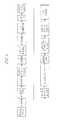
- FIG. 1is a flowchart of a sequential lamination process for manufacturing a printed circuit board having stacked vias including expensive and time consuming sequential lamination and plating steps.
- One embodiment of the inventionprovides a method of manufacturing a printed circuit board including providing a core subassembly including at least one metal layer carrier, providing a plurality of one-metal layer carriers after parallel processing each of the plurality of one-metal layer carriers, where the parallel processing of at least one of the plurality of one-metal layer carriers includes imaging photo resist onto at least one part of a substrate having at least one copper foil formed on a first surface of the substrate, etching portions of the at least one copper foil from the substrate, removing the at least one photo resist to expose the at least one part of the at least one copper foil thereby forming at least one copper foil pad, applying a lamination adhesive to a second surface of the substrate, applying a protective film to the lamination adhesive, forming at least one micro via in the second surface of the substrate to expose the at least one copper foil pad, filling conductive paste into the at least one micro via
- Another embodiment of the inventionprovides a method of manufacturing a printed circuit board including providing a core subassembly including at least one metal layer carrier, providing a plurality of one-metal layer carriers after parallel processing each of the plurality of one-metal layer carriers, where the parallel processing of at least one of the plurality of one-metal layer carriers includes imaging photo resist onto at least one part of a substrate having at least one copper foil formed on a first surface of the substrate, etching portions of the at least one copper foil from the substrate, removing the at least one photo resist to expose the at least one part of the at least one copper foil thereby forming at least one copper foil pad, applying a lamination adhesive to a second surface of the substrate, applying a protective film to the lamination adhesive, forming at least one micro via in the second surface of the substrate to expose the at least one copper foil pad, filling conductive paste into the at least one micro via, and removing the protective film to expose the lamination adhesive on the substrate for attachment, attaching at least two of the plurality of one-metal
- Still another embodiment of the inventionprovides a method of manufacturing a printed circuit board including providing a core subassembly including at least one metal layer carrier, attaching a plurality of one-metal layer carriers with each other after parallel processing each of the plurality of one-metal layer carriers to form a first subassembly, where the parallel processing of at least one of the plurality of one-metal layer carriers includes imaging photo resist onto at least one part of a substrate having at least one copper foil formed on a first surface of the substrate, etching portions of the at least one copper foil from the substrate, removing the at least one photo resist to expose the at least one part of the at least one copper foil thereby forming at least one copper foil pad, applying a lamination adhesive to a second surface of the substrate, applying a protective film to the lamination adhesive, forming at least one micro via in the second surface of the substrate to expose the at least one copper foil pad, filling conductive paste into the at least one micro via, and removing the protective film to expose the lamination adhesive on the substrate for
- FIG. 1is a flowchart of a sequential lamination process for manufacturing a printed circuit board having stacked vias including sequential lamination and plating steps.
- FIG. 2is a flowchart of a process for manufacturing a printed circuit board having stacked vias including a single lamination process in accordance with one embodiment of the present invention.
- FIGS. 3 a - 3 gillustrate a process for manufacturing a single metal layer substrate for a printed circuit board to be used in a single lamination cycle or process sequence with stacked (or staggered) micro vias in accordance with one embodiment of the present invention.
- FIG. 4 ais a cross sectional exploded view of a mixed printed circuit board including four etched single metal layer substrates and two non-etched single metal layer substrates of the substrates of FIGS. 3 a - 3 g sandwiching a core subassembly in accordance with one embodiment of the present invention.
- FIG. 4 bis a cross sectional exploded view of a mixed printed circuit board including six of the etched single metal layer substrates of FIG. 3 g sandwiching a core subassembly in accordance with one embodiment of the present invention.
- FIG. 4 cis a cross sectional exploded view of a mixed printed circuit board including six of the single metal layer substrates of FIG. 3 g in a pre-compressed form sandwiching a core subassembly in accordance with one embodiment of the present invention.
- FIG. 5is a cross sectional view of a finalized mixed printed circuit board of FIG. 4 b or 4 c.
- FIG. 6is a cross sectional view of a mixed printed circuit board including an outer buildup layer sandwiching two single metal layer substrates on both sides of a four metal layer core subassembly in accordance with one embodiment of the present invention.
- FIG. 7is a cross sectional view of a mixed printed circuit board including one buildup layer attached to one of two single metal layer substrates sandwiching a four metal layer core subassembly in accordance with one embodiment of the present invention.
- FIG. 8is a cross sectional view of a mixed printed circuit board including six of the single metal layer substrates of FIG. 3 g sandwiching a core subassembly including an active device in accordance with one embodiment of the present invention.
- FIG. 9is a cross sectional view of a mixed printed circuit board including six of the single metal layer substrates of FIG. 3 g sandwiching a core subassembly including an active device in accordance with one embodiment of the present invention.
- FIG. 10is a cross sectional view of a printed circuit board assembly including cutout regions that will isolate the flexible portion of the assembly from the rigid section in accordance with one embodiment of the present invention.
- FIG. 2is a flowchart of a process for manufacturing a printed circuit board having stacked vias including a single lamination process in accordance with one embodiment of the present invention.
- the single lamination process of FIG. 2includes a substantially fewer number of process steps. More specifically, the single lamination process of FIG. 2 eliminates a number of laminating and plating process steps required of sequential lamination processes for manufacturing multi-layer printed circuit boards. Aspects of single lamination processes for manufacturing circuit boards are further described in U.S. Pat. No. 7,523,545 and U.S. Prov. Patent Appl. Ser. No. 61/189,171, the entire content of each document is incorporated herein by reference.
- the processperforms a number of process steps related to printed circuit boards. In other embodiments, other suitable printed circuit board techniques can be used instead of those illustrated, including traditional PCB manufacturing techniques.
- the processdoes not perform all of the actions described. In other embodiments, the process performs additional actions. In one embodiment, the process performs the actions in a different order than illustrated. In some embodiments, the process performs some of the actions simultaneously. In one embodiment, the process goes directly from “LAYUP AND LAMINATE” to “FINAL FINISH”. In one embodiment, “DEVELOP, PLATE, STRIP, ETCH, STRIP” is replaced by “DEVELOP, ETCH, STRIP”.
- FIGS. 3 a - 3 gillustrate a process for manufacturing a single metal layer substrate for a printed circuit board to be used in a single lamination cycle or process sequence with stacked (or staggered) micro vias in accordance with one embodiment of the present invention.
- a two-sided substrate or carrier 10is prepared.
- the substrate 10includes a copper foil 10 a formed on opposite sides or surfaces of the substrate 10 and a core material 10 b made of metal, ceramic, or insulating material (e.g., FR4, LCP, Thermount, BT, GPY, such as Teflon, thermally conducting carbon (stablecor), halogen free insulating material, etc., where GPY is a laminate that does not fit in the FR4 category, such as polyimide, polyimide film such as Kapton®, aziridine cured epoxy, bismalimide, and other electrical grades of laminate).
- FR4 categorysuch as polyimide, polyimide film such as Kapton®, aziridine cured epoxy, bismalimide, and other electrical grades of laminate.
- the present inventionis not thereby limited.
- a single sided core or substratehaving a copper foil (e.g., a single foil 10 a ) formed on only one side of the substrate.
- a copper foile.g., a single foil 10 a
- other suitable substrate and conductive layer materialscan be used.
- the substrate 10has a thickness ranging from 3 to 4 mils (or about 3 to 4 mils).
- the substrate and other componentscan have other suitable dimensions.
- two photo resists 20are imaged onto the substrate 10 .
- the two photo resists 20 shownare laser-direct-imaged (or printed) onto one side of the substrate 10 (i.e., the bottom side).
- the present inventionis not thereby limited.
- the two photo resistscan be imaged using any suitable printing technique, such as photo, silkscreen, offset, inkjet, and the like. In other embodiments, more than or less than two photo resists can be imaged onto the substrate.
- the copper foil 10 ais etched from the substrate 10 with the exception of the parts of the copper foil 10 a covered by the two photo resists 20 , which are then stripped off to expose corresponding copper foil pads 11 .
- the present inventionis not thereby limited.
- one or more one-metal layer carrierse.g., one or more single sided circuits
- a metal platee.g., a stainless steel plate
- a copper flash(about five microns) is electrolytic flash plated onto one or more sides the metal plate.
- One or more photo resistsare applied to the one or more flash surfaces of the metal plate.
- the photo resistsare then imaged (e.g., negative imaged) to develop one or more cavities. Copper is then plated into the cavities.
- the photo resistsare then stripped off to form one or more copper foil pads for one or more circuit layers.
- one or more prepregsare applied on the copper foil pads to laminate the prepregs and the metal plate.
- the prepregsare then cured.
- the prepregsare thus laminated and cured with the metal plate, the copper foil pads and the copper flashes therebetween.
- the copper foil pads and the copper flashes with the cured prepregsare then peeled from the metal plate.
- the copper flashesare then etched off to expose the copper foil pads on the cured prepregs.
- a protective film (or Mylar sheet) 40 shown in FIG. 3 dis attached to the core material 10 b of the substrate 10 (or cured prepreg) with a lamination adhesive (or prepreg or uncured prepreg) 30 interposed between the Mylar sheet 40 and the core material 10 b .
- the protective layer or Mylar sheet 40is shown to be attached to the side of the substrate 10 opposite to the side of the substrate 10 where the two copper foil pads 11 are located.
- the protective film of the present inventionis not limited to only Mylar sheets, and can be made of any suitable material, such as polyester, oriented polypropylene, polyvinylfluoride, polyethylene, high density polyethylene, polyethylene napthalate, pacothane, polymethylpentene, or combinations thereof.
- via or micro via holes 50are formed in the substrate 10 (or cured prepreg).
- Each of the micro via holes 50is formed by laser drilling (and/or mechanical drilling) a hole having a diameter ranging from 4 to 10 mils (or about 4 to 10 mils) into the substrate 10 (or the cured prepreg).
- the micro via holes having other suitable diameterscan be used.
- the via or micro via holescan be created using a photo imagable dielectric process, plasma process, stamping process, or other suitable via generation processes.
- a conductive paste (or ink) 60is filled into each of the micro vias 50 formed in the substrate 10 (or cured prepreg), and in FIG. 3 g , the Mylar sheet 40 is then peeled off to form a one-metal layer carrier 70 for lay-up and lamination.
- the metal layer carriercan include additional layers or components.
- the metal layer carriercan include a buried resistor or a buried capacitor implemented using specific layers or laminations.
- the metal layer carrierscan also include surface treatments including, without limitation, organometal, immersion gold, immersion silver, immersion tin, and/or outer copper prior to adhesive. These surface treatments can improve both electrical and thermal conductivity.
- the metal layer carrierscan be laminated using various lamination machines, including, without limitation, a cut sheet laminator, a lamination press, a hot roll laminator, a vacuum laminator, a quick lamination press, or other suitable lamination machines.
- FIG. 4 ais a cross sectional exploded view of a mixed printed circuit board 100 - 1 including four etched single metal layer substrates 70 - 1 and two non-etched single metal layer substrates 70 - 2 of the substrates of FIGS. 3 a - 3 g sandwiching a core subassembly 102 in accordance with one embodiment of the present invention.
- the outer single metal layer substrates or non-etched substrates 70 - 2have a non-etched layer of copper on the outer surfaces thereof.
- the inner single metal layer substrates 70 - 1have etched layers of copper on the outer surfaces thereof.
- the core subassembly 102has four metal layers and two plated or filled through-hole vias 104 formed using a lamination process. In other embodiments, core subassembly 102 includes more than or less than two vias including through-hole vias and/or micro vias.
- the single metal layer substrates or carriers ( 70 - 1 , 70 - 2 )each include multiple micro vias 150 filled with conductive paste forming two stacked vias per assembly. To assemble the mixed PCB 100 , the single metal layer substrates ( 70 - 1 , 70 - 2 ) can be aligned above and below the core subassembly 102 and can all be pressed together to sandwich the subassembly 102 using one or more adhesive layers.
- the core subassemblyhas four metal layer carriers. In other embodiments, the core subassembly has more then or less than four metal layer carriers. In one such case, the core subassembly is assembled using a process involving only one lamination. In another such embodiment, the core subassembly is assembled using a process involving no lamination (e.g., the core subassembly has no vias). In some embodiments, the layers of the core subassembly are laminated at the time the one metal layer carriers are laminated together to form the PCB. In other embodiments, the layers of the core subassembly are laminated before the single metal layer carriers are laminated together to form the mixed PCB.
- three single metal layer carriersare positioned above and three single metal layer carriers are positioned below the core subassembly. In other embodiments, more than or less than three single metal layer carriers can be positioned above the core subassembly. Similarly, in other embodiments, more than or less than three single metal layer carriers can be positioned below the core subassembly. In one embodiment, one or more core subassembly layers are replaced with a single metal layer substrate having conductive paste micro vias. In the embodiment illustrated in FIG. 4 a , the mixed PCB includes two stacked vias. In other embodiments, the mixed PCB can have more then or less than two stacked vias.
- FIG. 4 bis a cross sectional exploded view of a mixed printed circuit board 100 - 2 including six of the etched single metal layer substrates 70 - 1 of FIG. 3 g sandwiching a core subassembly in accordance with one embodiment of the present invention.
- FIG. 4 bis substantially similar to FIG. 4 a except that the outer single metal layer carriers are etched in accordance with the process described in FIGS. 3 a - 3 g rather than non-etched as in FIG. 4 a .
- FIG. 4 bcan operate as described above for FIG. 4 a .
- one stack of micro vias 151is aligned with one through hole via 104 below, while the other micro vias 150 are offset from the through hole vias 104 .
- FIG. 4 cis a cross sectional exploded view of a mixed printed circuit board 100 - 3 including six of the single metal layer substrates 70 - 1 of FIG. 3 g in a pre-compressed form sandwiching a core subassembly in accordance with one embodiment of the present invention.
- the precompressed formincludes an upper assembly 80 - 1 including three of the six single metal layer substrates 70 - 1 and a lower assembly 80 - 2 including three of the six single metal layer substrates 70 - 1 .
- the embodiment of FIG. 4 cis similar to that of FIG. 4 b except that the single metal layer substrates of FIG. 4 b begin in a compressed state. In other respects, FIG. 4 c can operate as described above for FIG. 4 b.
- FIG. 5is a cross sectional view of a finalized mixed printed circuit board 100 - 4 in accordance with the embodiments of FIG. 4 b or 4 c .
- a finalized mixed printed circuit board for FIG. 4 awould appear similar to FIG. 5 , except the outer layers would include the non-etched copper.
- FIG. 6is a cross sectional view of a mixed PCB 200 including a buildup layer 270 - 2 sandwiching two single metal layer substrates 270 - 1 on both sides of a four metal layer core subassembly 202 in accordance with one embodiment of the present invention.
- the mixed PCB 200includes benefits from both sequential lamination board manufacturing processes and single lamination board manufacturing processes.
- the mixed PCB 200can provide outer surfaces that are substantially or exactly flat. In some embodiments, these substantially or exactly flat surfaces can be highly desirable.
- the process of manufacturing the mixed PCB 200can drastically improve manufacturing time and expense by eliminating various lamination and plating steps.
- the four single metal layer substrates 270 - 1include multiple stacked micro vias 250 and can be formed using any of the processes described above.
- the four metal layer core subassembly 202includes multiple through-hole vias 204 and can be formed using the sequential lamination processes described above. In some embodiments, the through-hole vias are replaced with micro vias that are filled with either copper or conductive paste.
- the two buildup layers 270 - 2include multiple plated or filled micro vias (e.g., through-hole vias) 284 and can be formed using processes for manufacturing PCBs described in FIG. 1 .
- the PCBincludes two single metal layer substrates above and below the core subassembly. In other embodiments, the PCB can include more than two single metal layer substrates. In the embodiment illustrated in FIG. 6 , one buildup layer 270 - 2 is positioned above and one buildup layer 270 - 2 is positioned below the single metal layer substrates. In other embodiments, more than one buildup layer can be positioned above and more than one buildup layer can be positioned below the single metal layer substrates. In one embodiment, one or more of the buildup layers are replaced with another layer of one of the single metal layer substrates or removed all together.
- a four metal layer core subassembly 202is positioned in the center of the mixed PCB 200 .
- the core subassemblycan include more than or less than four layers.
- the four metal layer core subassemblyincludes two plated or filled through-hole vias 204 .
- the core subassemblycan implemented with more than or less than two vias. In one such embodiment, the core subassembly can implemented without any vias.
- the mixed PCBincludes two stacked vias. In other embodiments, the mixed PCB can have more then or less than two stacked vias.
- core subassemblies 102 and 202include two through hole vias ( 104 , 204 ) per subassembly that are offset from stacked vias 150 of the single metal layer substrates ( 70 - 1 , 270 - 1 ).
- core subassemblies 102 and 202can include one or more micro vias.
- the micro viasare filled with conductive paste, conductive ink or copper.
- the conductive ink micro viashave a trapezoidal cross section where a wider opening of the micro via is closest to a central line of the core subassembly (see for example, the orientation of micro via 150 in FIG. 5 ).
- the through hole vias of the subassemblies 102 and 202are not offset from the stacked vias of the single metal layer substrates.
- FIG. 7is a cross sectional view of a mixed PCB 300 including one buildup layer 270 - 2 attached to two of four single metal layer substrates 270 - 1 sandwiching a four metal layer core subassembly 202 in accordance with one embodiment of the present invention.
- the mixed PCB 300includes the buildup layer 270 - 2 sandwiching two single metal layer substrates 270 - 1 on one side of the core subassembly 202 .
- the mixed PCB 300further includes two single metal layer substrates 270 - 1 sandwiching the four layer core subassembly 202 on the other side of the core subassembly 202 .
- the embodiment illustrated in FIG. 7is similar to that of FIG. 6 except that one of the outer buildup layers has been removed.
- one or both of the upper single metal layer carriers 270 - 1can also be removed.
- the structure of the mixed PCB of FIG. 7can be modified in a manner similar to the modifications described above for the mixed PCB of FIG. 6 .
- FIG. 8is a cross sectional view of a mixed printed circuit board 400 including six of the single metal layer substrates ( 470 - 1 , 470 - 2 ) of FIG. 3 g sandwiching a core subassembly 402 including an active device 406 in accordance with one embodiment of the present invention.
- the mixed PCB 400 illustrated in FIG. 8is similar to that of FIG. 5 except that the core subassembly 402 includes the embedded active device 406 and the upper single metal layer substrates 470 - 2 include additional micro vias 450 forming a stacked via for connection to the active device 406 .
- the active device 406can be a transistor, integrated circuit, or other active device commonly used in conjunction with a printed circuit board. In the embodiment illustrated in FIG.
- the mixed PCB 400includes a single active device 406 .
- additional active devicescan be used along with additional vias to support various connections needed.
- the structure of the mixed PCB of FIG. 8can be modified in a manner similar to the modifications described above for the mixed PCBs of FIGS. 4 a , 4 b , 4 c , 5 and 6 .
- the active devicecan be located on or within one of the single metal layer substrates. In another embodiment, active devices can be located on or within any of the single metal layer substrates and the core subassembly.
- FIG. 9is a cross sectional view of a mixed printed circuit board 500 including two of the single metal layer substrates ( 570 - 1 , 570 - 2 ) of FIG. 3 g sandwiching a core subassembly 502 including an active device 506 in accordance with one embodiment of the present invention.
- the PCB illustrated in FIG. 9is substantially similar to that of FIG. 8 except that it includes an additional via 584 to connect the active device 506 which is embedded further within the core assembly 502 than in FIG. 8 .
- the mixed PCB of FIG. 9can function and be modified as the mixed PCB of FIG. 8 .
- FIG. 10is a cross sectional view of a printed circuit board assembly 600 including cutout regions that will isolate the flexible portion 606 of the assembly from the rigid sections ( 602 , 604 ) in accordance with one embodiment of the present invention.
- Vias 608can provide electrical interconnects between the various flexible, rigid, and rigid-flex layers.
- the circuit board assembly 600can be formed using any of the manufacturing processes described herein, including, for example, the single lamination processes described above in FIGS. 3 a - 3 g , 4 a - 4 c .
- Conventional lamination processesincluding sequential lamination type processes, require a relatively large number of process steps that can damage a flexible or rigid-flex substrate during the manufacturing process. More specifically, conventional process steps such as plating, cleaning, scrubbing, and planarization can damage flexible or rigid-flex substrates and cause problems related to establishing certain positional tolerances.
- the circuit board assembly 600can be formed while avoiding or substantially reducing numerous iterative steps common to the conventional processes, including, for example, the intrusive plating, cleaning, scrubbing, and planarization process steps.
- the manufacturing processes described hereincan be used in conjunction with a number of technologies, including, without limitation, flip chip, MEMS circuits, ceramic packages, organic packages, high density substrates, BGA substrates, rigid substrates, flexible substrates, and rigid-flex substrates.
Landscapes
- Engineering & Computer Science (AREA)
- Manufacturing & Machinery (AREA)
- Microelectronics & Electronic Packaging (AREA)
- Production Of Multi-Layered Print Wiring Board (AREA)
Abstract
Description
Claims (17)
Priority Applications (2)
| Application Number | Priority Date | Filing Date | Title |
|---|---|---|---|
| US12/772,086US8020292B1 (en) | 2010-04-30 | 2010-04-30 | Methods of manufacturing printed circuit boards |
| US13/206,414US8863379B2 (en) | 2010-04-30 | 2011-08-09 | Methods of manufacturing printed circuit boards using parallel processes to interconnect with subassemblies |
Applications Claiming Priority (1)
| Application Number | Priority Date | Filing Date | Title |
|---|---|---|---|
| US12/772,086US8020292B1 (en) | 2010-04-30 | 2010-04-30 | Methods of manufacturing printed circuit boards |
Related Child Applications (1)
| Application Number | Title | Priority Date | Filing Date |
|---|---|---|---|
| US13/206,414ContinuationUS8863379B2 (en) | 2010-04-30 | 2011-08-09 | Methods of manufacturing printed circuit boards using parallel processes to interconnect with subassemblies |
Publications (1)
| Publication Number | Publication Date |
|---|---|
| US8020292B1true US8020292B1 (en) | 2011-09-20 |
Family
ID=44586987
Family Applications (2)
| Application Number | Title | Priority Date | Filing Date |
|---|---|---|---|
| US12/772,086ActiveUS8020292B1 (en) | 2010-04-30 | 2010-04-30 | Methods of manufacturing printed circuit boards |
| US13/206,414Active2032-03-25US8863379B2 (en) | 2010-04-30 | 2011-08-09 | Methods of manufacturing printed circuit boards using parallel processes to interconnect with subassemblies |
Family Applications After (1)
| Application Number | Title | Priority Date | Filing Date |
|---|---|---|---|
| US13/206,414Active2032-03-25US8863379B2 (en) | 2010-04-30 | 2011-08-09 | Methods of manufacturing printed circuit boards using parallel processes to interconnect with subassemblies |
Country Status (1)
| Country | Link |
|---|---|
| US (2) | US8020292B1 (en) |
Cited By (13)
| Publication number | Priority date | Publication date | Assignee | Title |
|---|---|---|---|---|
| US20090159317A1 (en)* | 2007-12-19 | 2009-06-25 | Fukui Precision Component (Shenzhen) Co., Ltd. | Printed circuit board and method for manufacturing the same |
| US20110041330A1 (en)* | 2006-04-19 | 2011-02-24 | Dynamic Details, Inc. | Methods of manufacturing printed circuit boards with stacked micro vias |
| US20110289774A1 (en)* | 2010-04-30 | 2011-12-01 | Rajesh Kumar | Methods of manufacturing printed circuit boards using parallel processes to interconnect with subassemblies |
| US8664656B1 (en) | 2012-10-04 | 2014-03-04 | Apple Inc. | Devices and methods for embedding semiconductors in printed circuit boards |
| US20140304977A1 (en)* | 2011-12-30 | 2014-10-16 | Shenzhen Suntak Multilayer Pcb Co., Ltd. | Fabrication process of stepped circuit board |
| US20150053463A1 (en)* | 2013-08-26 | 2015-02-26 | Unimicron Technology Corp. | Rigid flex board module and the manufacturing method thereof |
| US20160369649A1 (en)* | 2012-06-05 | 2016-12-22 | General Electric Company | High temperature flame sensor |
| US20170273195A1 (en)* | 2016-03-21 | 2017-09-21 | Multek Technologies Limited | Recessed cavity in printed circuit board protected by lpi |
| US10321560B2 (en) | 2015-11-12 | 2019-06-11 | Multek Technologies Limited | Dummy core plus plating resist restrict resin process and structure |
| US10772220B2 (en) | 2016-02-17 | 2020-09-08 | Multek Technologies Limited | Dummy core restrict resin process and structure |
| WO2021102898A1 (en)* | 2019-11-29 | 2021-06-03 | 鹏鼎控股(深圳)股份有限公司 | Multi-layer circuit board, and manufacturing method for same |
| US11219129B2 (en)* | 2019-01-31 | 2022-01-04 | At&S (China) Co. Ltd. | Component carrier with blind hole filled with an electrically conductive medium and fulfilling a minimum thickness design rule |
| US11324108B2 (en)* | 2018-08-31 | 2022-05-03 | Murata Manufacturing Co., Ltd. | Wiring substrate and module |
Families Citing this family (10)
| Publication number | Priority date | Publication date | Assignee | Title |
|---|---|---|---|---|
| JP5352437B2 (en)* | 2009-11-30 | 2013-11-27 | ルネサスエレクトロニクス株式会社 | Manufacturing method of semiconductor device |
| US8921703B2 (en)* | 2012-02-17 | 2014-12-30 | Htc Corporation | Circuit board, structural unit thereof and manufacturing method thereof |
| JP6291738B2 (en) | 2013-07-25 | 2018-03-14 | 富士通株式会社 | CIRCUIT BOARD, CIRCUIT BOARD MANUFACTURING METHOD, AND ELECTRONIC DEVICE |
| US20200279814A1 (en)* | 2019-02-28 | 2020-09-03 | Advanced Semiconductor Engineering, Inc. | Wiring structure and method for manufacturing the same |
| JP7031955B2 (en)* | 2019-09-10 | 2022-03-08 | Fict株式会社 | Circuit board manufacturing method |
| CN111328217B (en)* | 2020-04-09 | 2021-09-17 | 江苏普诺威电子股份有限公司 | MEMS packaging carrier plate stack structure and manufacturing method thereof |
| CN112543550A (en)* | 2020-11-17 | 2021-03-23 | 惠州市特创电子科技股份有限公司 | Multilayer circuit board, board body and processing method thereof |
| EP4040926A1 (en) | 2021-02-09 | 2022-08-10 | AT & S Austria Technologie & Systemtechnik Aktiengesellschaft | Component carriers connected by staggered interconnect elements |
| KR20220160967A (en)* | 2021-05-28 | 2022-12-06 | (주)티에스이 | multi-layer printed circuit board made of different materials and manufacturing method of the same |
| CN118201251B (en)* | 2024-05-17 | 2024-08-27 | 浙江万正电子科技股份有限公司 | Manufacturing method of third-order blind buried hole printed board |
Citations (17)
| Publication number | Priority date | Publication date | Assignee | Title |
|---|---|---|---|---|
| US5481795A (en)* | 1992-05-06 | 1996-01-09 | Matsushita Electric Industrial Co., Ltd. | Method of manufacturing organic substrate used for printed circuits |
| US5613033A (en) | 1995-01-18 | 1997-03-18 | Dell Usa, Lp | Laminated module for stacking integrated circuits |
| US5939789A (en)* | 1994-02-28 | 1999-08-17 | Hitachi, Ltd. | Multilayer substrates methods for manufacturing multilayer substrates and electronic devices |
| US6000129A (en) | 1996-06-28 | 1999-12-14 | International Business Machines Corporation | Process for manufacturing a circuit with filled holes |
| US6211487B1 (en)* | 1993-09-22 | 2001-04-03 | Matsushita Electric Industrial Co., Ltd. | Printed circuit board and method of manufacturing the same |
| US6222740B1 (en) | 1997-12-19 | 2001-04-24 | Robert Bosch Gmbh | Multilayer circuit board having at least one core substrate arranged therein |
| US6440542B1 (en) | 1999-12-08 | 2002-08-27 | Ibiden Co., Ltd. | Copper-clad laminated board, and circuit board for printed wiring board and method for producing the same |
| US6555761B2 (en) | 2000-12-29 | 2003-04-29 | Intel Corporation | Printed circuit board with solder-filled via |
| US6631558B2 (en) | 1996-06-05 | 2003-10-14 | Laservia Corporation | Blind via laser drilling system |
| US6779262B1 (en) | 1999-03-23 | 2004-08-24 | Circuit Foil Luxembourg Trading Sarl | Method for manufacturing a multilayer printed circuit board |
| US20050016768A1 (en) | 2003-07-24 | 2005-01-27 | Zollo James A. | Inverted microvia structure and method of manufacture |
| US6889433B1 (en)* | 1999-07-12 | 2005-05-10 | Ibiden Co., Ltd. | Method of manufacturing printed-circuit board |
| US6954986B2 (en) | 2000-03-31 | 2005-10-18 | Dyconex Ag | Method for fabricating electrical connecting element |
| US20070196953A1 (en) | 2005-05-05 | 2007-08-23 | International Business Machines Corporation | Method and apparatus for forming stacked die and substrate structures for increased packing density |
| US7260890B2 (en) | 2002-06-26 | 2007-08-28 | Georgia Tech Research Corporation | Methods for fabricating three-dimensional all organic interconnect structures |
| US20070246254A1 (en) | 2006-04-19 | 2007-10-25 | Raj Kumar | Printed circuit boards with stacked micro vias |
| US7402758B2 (en) | 2003-10-09 | 2008-07-22 | Qualcomm Incorporated | Telescoping blind via in three-layer core |
Family Cites Families (1)
| Publication number | Priority date | Publication date | Assignee | Title |
|---|---|---|---|---|
| US8020292B1 (en)* | 2010-04-30 | 2011-09-20 | Ddi Global Corp. | Methods of manufacturing printed circuit boards |
- 2010
- 2010-04-30USUS12/772,086patent/US8020292B1/enactiveActive
- 2011
- 2011-08-09USUS13/206,414patent/US8863379B2/enactiveActive
Patent Citations (18)
| Publication number | Priority date | Publication date | Assignee | Title |
|---|---|---|---|---|
| US5481795A (en)* | 1992-05-06 | 1996-01-09 | Matsushita Electric Industrial Co., Ltd. | Method of manufacturing organic substrate used for printed circuits |
| US6211487B1 (en)* | 1993-09-22 | 2001-04-03 | Matsushita Electric Industrial Co., Ltd. | Printed circuit board and method of manufacturing the same |
| US5939789A (en)* | 1994-02-28 | 1999-08-17 | Hitachi, Ltd. | Multilayer substrates methods for manufacturing multilayer substrates and electronic devices |
| US5613033A (en) | 1995-01-18 | 1997-03-18 | Dell Usa, Lp | Laminated module for stacking integrated circuits |
| US6631558B2 (en) | 1996-06-05 | 2003-10-14 | Laservia Corporation | Blind via laser drilling system |
| US6000129A (en) | 1996-06-28 | 1999-12-14 | International Business Machines Corporation | Process for manufacturing a circuit with filled holes |
| US6222740B1 (en) | 1997-12-19 | 2001-04-24 | Robert Bosch Gmbh | Multilayer circuit board having at least one core substrate arranged therein |
| US6779262B1 (en) | 1999-03-23 | 2004-08-24 | Circuit Foil Luxembourg Trading Sarl | Method for manufacturing a multilayer printed circuit board |
| US6889433B1 (en)* | 1999-07-12 | 2005-05-10 | Ibiden Co., Ltd. | Method of manufacturing printed-circuit board |
| US6440542B1 (en) | 1999-12-08 | 2002-08-27 | Ibiden Co., Ltd. | Copper-clad laminated board, and circuit board for printed wiring board and method for producing the same |
| US6954986B2 (en) | 2000-03-31 | 2005-10-18 | Dyconex Ag | Method for fabricating electrical connecting element |
| US6555761B2 (en) | 2000-12-29 | 2003-04-29 | Intel Corporation | Printed circuit board with solder-filled via |
| US7260890B2 (en) | 2002-06-26 | 2007-08-28 | Georgia Tech Research Corporation | Methods for fabricating three-dimensional all organic interconnect structures |
| US20050016768A1 (en) | 2003-07-24 | 2005-01-27 | Zollo James A. | Inverted microvia structure and method of manufacture |
| US7402758B2 (en) | 2003-10-09 | 2008-07-22 | Qualcomm Incorporated | Telescoping blind via in three-layer core |
| US20070196953A1 (en) | 2005-05-05 | 2007-08-23 | International Business Machines Corporation | Method and apparatus for forming stacked die and substrate structures for increased packing density |
| US20070246254A1 (en) | 2006-04-19 | 2007-10-25 | Raj Kumar | Printed circuit boards with stacked micro vias |
| US7523545B2 (en) | 2006-04-19 | 2009-04-28 | Dynamic Details, Inc. | Methods of manufacturing printed circuit boards with stacked micro vias |
Non-Patent Citations (2)
| Title |
|---|
| International Search Report for Application No. PCT/US10/033295 filed Apr. 30, 2010, dated Jul. 9, 2010, mailed Jul. 29, 2010, 2 pages. |
| Written Opinion for Application No. PCT/US10/033295 filed Apr. 30, 2010, dated Jul. 9, 2010, mailed Jul. 29, 2010, 5 pages. |
Cited By (24)
| Publication number | Priority date | Publication date | Assignee | Title |
|---|---|---|---|---|
| US8950063B2 (en)* | 2006-04-19 | 2015-02-10 | Viasystems Technologies Corp., L.L.C. | Methods of manufacturing printed circuit boards with stacked micro vias |
| US20110041330A1 (en)* | 2006-04-19 | 2011-02-24 | Dynamic Details, Inc. | Methods of manufacturing printed circuit boards with stacked micro vias |
| US9485876B2 (en)* | 2006-04-19 | 2016-11-01 | Viasystems Technologies Corp., L.L.C. | Methods of manufacturing printed circuit boards with stacked micro vias |
| US20150041428A1 (en)* | 2006-04-19 | 2015-02-12 | Viasystems Technologies Corp., L.L.C. | Methods of manufacturing printed circuit boards with stacked micro vias |
| US8205330B2 (en)* | 2007-12-19 | 2012-06-26 | Fukui Precision Component (Shenzhen) Co., Ltd. | Method for manufacturing a printed circuit board |
| US20090159317A1 (en)* | 2007-12-19 | 2009-06-25 | Fukui Precision Component (Shenzhen) Co., Ltd. | Printed circuit board and method for manufacturing the same |
| US20110289774A1 (en)* | 2010-04-30 | 2011-12-01 | Rajesh Kumar | Methods of manufacturing printed circuit boards using parallel processes to interconnect with subassemblies |
| US8863379B2 (en)* | 2010-04-30 | 2014-10-21 | Viasystems Technologies Corp., L.L.C. | Methods of manufacturing printed circuit boards using parallel processes to interconnect with subassemblies |
| US20140304977A1 (en)* | 2011-12-30 | 2014-10-16 | Shenzhen Suntak Multilayer Pcb Co., Ltd. | Fabrication process of stepped circuit board |
| US9713261B2 (en)* | 2011-12-30 | 2017-07-18 | Shenzhen Suntak Multilayer Pcb Co., Ltd. | Fabrication process of stepped circuit board |
| US20160369649A1 (en)* | 2012-06-05 | 2016-12-22 | General Electric Company | High temperature flame sensor |
| US10392959B2 (en)* | 2012-06-05 | 2019-08-27 | General Electric Company | High temperature flame sensor |
| US8664656B1 (en) | 2012-10-04 | 2014-03-04 | Apple Inc. | Devices and methods for embedding semiconductors in printed circuit boards |
| US8809859B2 (en) | 2012-10-04 | 2014-08-19 | Apple Inc. | Devices and methods for embedding semiconductors in printed circuit boards |
| US9253898B2 (en)* | 2013-08-26 | 2016-02-02 | Unimicron Technology Corp. | Rigid flex board module and the manufacturing method thereof |
| US20150053463A1 (en)* | 2013-08-26 | 2015-02-26 | Unimicron Technology Corp. | Rigid flex board module and the manufacturing method thereof |
| US10321560B2 (en) | 2015-11-12 | 2019-06-11 | Multek Technologies Limited | Dummy core plus plating resist restrict resin process and structure |
| US10772220B2 (en) | 2016-02-17 | 2020-09-08 | Multek Technologies Limited | Dummy core restrict resin process and structure |
| US20170273195A1 (en)* | 2016-03-21 | 2017-09-21 | Multek Technologies Limited | Recessed cavity in printed circuit board protected by lpi |
| US10064292B2 (en)* | 2016-03-21 | 2018-08-28 | Multek Technologies Limited | Recessed cavity in printed circuit board protected by LPI |
| US11324108B2 (en)* | 2018-08-31 | 2022-05-03 | Murata Manufacturing Co., Ltd. | Wiring substrate and module |
| US11219129B2 (en)* | 2019-01-31 | 2022-01-04 | At&S (China) Co. Ltd. | Component carrier with blind hole filled with an electrically conductive medium and fulfilling a minimum thickness design rule |
| US11700690B2 (en) | 2019-01-31 | 2023-07-11 | At&S (China) Co. Ltd. | Component carrier with blind hole filled with an electrically conductive medium and fulfilling a minimum thickness design rule |
| WO2021102898A1 (en)* | 2019-11-29 | 2021-06-03 | 鹏鼎控股(深圳)股份有限公司 | Multi-layer circuit board, and manufacturing method for same |
Also Published As
| Publication number | Publication date |
|---|---|
| US8863379B2 (en) | 2014-10-21 |
| US20110289774A1 (en) | 2011-12-01 |
Similar Documents
| Publication | Publication Date | Title |
|---|---|---|
| US8020292B1 (en) | Methods of manufacturing printed circuit boards | |
| US7523545B2 (en) | Methods of manufacturing printed circuit boards with stacked micro vias | |
| TWI386140B (en) | Flexible multilayer circuit board | |
| JP5411362B2 (en) | Multilayer wiring board and manufacturing method thereof | |
| TWI392410B (en) | Multilayer printed wiring board and manufacturing method thereof | |
| US8567053B2 (en) | Methods of manufacturing printed circuit boards | |
| US8453322B2 (en) | Manufacturing methods of multilayer printed circuit board having stacked via | |
| US20130319740A1 (en) | Electronic component built-in substrate and method of manufacturing the same | |
| JP2011199077A (en) | Method of manufacturing multilayer wiring board | |
| CN102119588A (en) | Method for manufacturing module with built-in component, and module with built-in component | |
| KR101694575B1 (en) | Methods of manufacturing printed circuit boards using parallel processes to interconnect with subassemblies | |
| JP2009224415A (en) | Method of manufacturing multilayer wiring board, and intermediate product of multilayer wiring board, | |
| JP3738536B2 (en) | Method for manufacturing printed wiring board | |
| JP4899409B2 (en) | Multilayer printed wiring board and manufacturing method thereof | |
| HK1183590A (en) | Methods of manufacturing printed circuit boards using parallel processes to interconnect with subassemblies | |
| KR20180025345A (en) | Rigid flexible circuit board manufacturing method | |
| TW201318500A (en) | Methods of manufacturing printed circuit boards using parallel processes to interconnect with subassemblies | |
| JP2006013172A (en) | Method for manufacturing multilayer wiring board | |
| HK1175348A (en) | Printed circuit boards with stacked micros vias and method of manufacturing the same | |
| HK1175348B (en) | Printed circuit boards with stacked micros vias and method of manufacturing the same | |
| TWM436298U (en) | Printed circuit boards |
Legal Events
| Date | Code | Title | Description |
|---|---|---|---|
| AS | Assignment | Owner name:DDI GLOBAL CORP., CALIFORNIA Free format text:ASSIGNMENT OF ASSIGNORS INTEREST;ASSIGNORS:KUMAR, RAJESH;DREYER, MONTE P.;TAYLOR, MICHAEL J.;SIGNING DATES FROM 20100716 TO 20100803;REEL/FRAME:024791/0117 | |
| AS | Assignment | Owner name:JPMORGAN CHASE BANK, N.A., AS ADMINISTRATIVE AGENT Free format text:SECURITY AGREEMENT;ASSIGNOR:DDI GLOBAL CORP.;REEL/FRAME:025321/0451 Effective date:20100923 | |
| STCF | Information on status: patent grant | Free format text:PATENTED CASE | |
| AS | Assignment | Owner name:DDI GLOBAL CORP., CALIFORNIA Free format text:RELEASE BY SECURED PARTY;ASSIGNOR:JPMORGAN CHASE BANK, N.A.,;REEL/FRAME:028425/0777 Effective date:20120621 | |
| AS | Assignment | Owner name:VIASYSTEMS NORTH AMERICA OPERATIONS, INC., MISSOUR Free format text:CHANGE OF NAME;ASSIGNOR:DDI GLOBAL CORP.;REEL/FRAME:031863/0129 Effective date:20130401 | |
| AS | Assignment | Owner name:VIASYSTEMS TECHNOLOGIES CORP., L.L.C., MISSOURI Free format text:ASSIGNMENT OF ASSIGNORS INTEREST;ASSIGNOR:VIASYSTEMS NORTH AMERICA OPERATIONS, INC.;REEL/FRAME:031937/0500 Effective date:20131231 | |
| FPAY | Fee payment | Year of fee payment:4 | |
| AS | Assignment | Owner name:JPMORGAN CHASE BANK, N.A., AS ADMINISTRATIVE AGENT Free format text:PATENT SECURITY AGREEMENT-TERM;ASSIGNORS:TTM TECHNOLOGIES, INC.;VIASYSTEMS, INC.;VIASYSTEMS TECHNOLOGIES CORP., L.L.C.;REEL/FRAME:035851/0928 Effective date:20150531 Owner name:JPMORGAN CHASE BANK, N.A., AS ADMINISTRATIVE AGENT Free format text:PATENT SECURITY AGREEMENT-ABL;ASSIGNORS:TTM TECHNOLOGIES, INC.;VIASYSTEMS, INC.;VIASYSTEMS TECHNOLOGIES CORP., L.L.C.;REEL/FRAME:035858/0890 Effective date:20150531 | |
| MAFP | Maintenance fee payment | Free format text:PAYMENT OF MAINTENANCE FEE, 8TH YEAR, LARGE ENTITY (ORIGINAL EVENT CODE: M1552); ENTITY STATUS OF PATENT OWNER: LARGE ENTITY Year of fee payment:8 | |
| AS | Assignment | Owner name:TTM TECHNOLOGIES NORTH AMERICA, LLC, CALIFORNIA Free format text:CHANGE OF NAME;ASSIGNOR:VIASYSTEMS TECHNOLOGIES CORP., L.L.C.;REEL/FRAME:050314/0305 Effective date:20171023 | |
| MAFP | Maintenance fee payment | Free format text:PAYMENT OF MAINTENANCE FEE, 12TH YEAR, LARGE ENTITY (ORIGINAL EVENT CODE: M1553); ENTITY STATUS OF PATENT OWNER: LARGE ENTITY Year of fee payment:12 | |
| AS | Assignment | Owner name:JPMORGAN CHASE BANK, N.A., AS ADMINISTRATIVE AGENT, ILLINOIS Free format text:PATENT SECURITY AGREEMENT (TERM LOAN);ASSIGNORS:TELEPHONICS CORPORATION;TTM TECHNOLOGIES, INC.;TTM TECHNOLOGIES NORTH AMERICA, LLC;REEL/FRAME:063804/0745 Effective date:20230530 Owner name:JPMORGAN CHASE BANK, N.A., AS ADMINISTRATIVE AGENT, ILLINOIS Free format text:PATENT SECURITY AGREEMENT (ABL);ASSIGNORS:TELEPHONICS CORPORATION;TTM TECHNOLOGIES, INC.;TTM TECHNOLOGIES NORTH AMERICA, LLC;REEL/FRAME:063804/0702 Effective date:20230530 |