US8017470B2 - Method of forming a structure over a semiconductor substrate - Google Patents
Method of forming a structure over a semiconductor substrateDownload PDFInfo
- Publication number
- US8017470B2 US8017470B2US12/803,296US80329610AUS8017470B2US 8017470 B2US8017470 B2US 8017470B2US 80329610 AUS80329610 AUS 80329610AUS 8017470 B2US8017470 B2US 8017470B2
- Authority
- US
- United States
- Prior art keywords
- region
- oxide layer
- substrate
- thickness
- over
- Prior art date
- Legal status (The legal status is an assumption and is not a legal conclusion. Google has not performed a legal analysis and makes no representation as to the accuracy of the status listed.)
- Expired - Fee Related
Links
- 239000000758substrateSubstances0.000titleclaimsabstractdescription91
- 238000000034methodMethods0.000titleclaimsabstractdescription26
- 239000004065semiconductorSubstances0.000titleclaimsabstractdescription26
- IJGRMHOSHXDMSA-UHFFFAOYSA-NAtomic nitrogenChemical compoundN#NIJGRMHOSHXDMSA-UHFFFAOYSA-N0.000claimsabstractdescription67
- 229910052757nitrogenInorganic materials0.000claimsabstractdescription35
- 150000002829nitrogenChemical class0.000claimsdescription15
- VYPSYNLAJGMNEJ-UHFFFAOYSA-NSilicium dioxideChemical compoundO=[Si]=OVYPSYNLAJGMNEJ-UHFFFAOYSA-N0.000abstractdescription38
- 239000000377silicon dioxideSubstances0.000abstractdescription19
- 235000012239silicon dioxideNutrition0.000abstractdescription19
- 229910052710siliconInorganic materials0.000abstractdescription16
- 239000010703siliconSubstances0.000abstractdescription16
- 239000002019doping agentSubstances0.000description18
- XUIMIQQOPSSXEZ-UHFFFAOYSA-NSiliconChemical compound[Si]XUIMIQQOPSSXEZ-UHFFFAOYSA-N0.000description15
- 239000004020conductorSubstances0.000description14
- 241000894007speciesSpecies0.000description13
- 239000000463materialSubstances0.000description11
- 229910021332silicideInorganic materials0.000description9
- 239000012634fragmentSubstances0.000description8
- FVBUAEGBCNSCDD-UHFFFAOYSA-Nsilicide(4-)Chemical compound[Si-4]FVBUAEGBCNSCDD-UHFFFAOYSA-N0.000description6
- 238000000429assemblyMethods0.000description4
- 230000000712assemblyEffects0.000description4
- 238000009792diffusion processMethods0.000description4
- -1for exampleChemical compound0.000description4
- 230000005012migrationEffects0.000description4
- 238000013508migrationMethods0.000description4
- 229910021420polycrystalline siliconInorganic materials0.000description4
- 230000015572biosynthetic processEffects0.000description3
- 238000006243chemical reactionMethods0.000description3
- 230000000873masking effectEffects0.000description3
- 229910021421monocrystalline siliconInorganic materials0.000description3
- 230000001590oxidative effectEffects0.000description3
- 230000035515penetrationEffects0.000description3
- 229920005591polysiliconPolymers0.000description3
- 102000004129N-Type Calcium ChannelsHuman genes0.000description2
- 108090000699N-Type Calcium ChannelsProteins0.000description2
- 229910052581Si3N4Inorganic materials0.000description2
- 238000005229chemical vapour depositionMethods0.000description2
- 230000002708enhancing effectEffects0.000description2
- 229910052751metalInorganic materials0.000description2
- 239000002184metalSubstances0.000description2
- 150000002739metalsChemical class0.000description2
- 230000003647oxidationEffects0.000description2
- 238000007254oxidation reactionMethods0.000description2
- 230000002093peripheral effectEffects0.000description2
- 238000005498polishingMethods0.000description2
- HQVNEWCFYHHQES-UHFFFAOYSA-Nsilicon nitrideChemical compoundN12[Si]34N5[Si]62N3[Si]51N64HQVNEWCFYHHQES-UHFFFAOYSA-N0.000description2
- 125000006850spacer groupChemical group0.000description2
- 229910021341titanium silicideInorganic materials0.000description2
- WQJQOUPTWCFRMM-UHFFFAOYSA-Ntungsten disilicideChemical compound[Si]#[W]#[Si]WQJQOUPTWCFRMM-UHFFFAOYSA-N0.000description2
- 229910021342tungsten silicideInorganic materials0.000description2
- 229910021417amorphous siliconInorganic materials0.000description1
- 238000010276constructionMethods0.000description1
- 230000000694effectsEffects0.000description1
- 238000005530etchingMethods0.000description1
- 230000005283ground stateEffects0.000description1
- 230000003993interactionEffects0.000description1
- 238000012986modificationMethods0.000description1
- 230000004048modificationEffects0.000description1
- 125000004433nitrogen atomChemical groupN*0.000description1
- QJGQUHMNIGDVPM-UHFFFAOYSA-Nnitrogen groupChemical group[N]QJGQUHMNIGDVPM-UHFFFAOYSA-N0.000description1
- 229920002120photoresistant polymerPolymers0.000description1
- 238000003672processing methodMethods0.000description1
Images


Classifications
- H—ELECTRICITY
- H10—SEMICONDUCTOR DEVICES; ELECTRIC SOLID-STATE DEVICES NOT OTHERWISE PROVIDED FOR
- H10D—INORGANIC ELECTRIC SEMICONDUCTOR DEVICES
- H10D84/00—Integrated devices formed in or on semiconductor substrates that comprise only semiconducting layers, e.g. on Si wafers or on GaAs-on-Si wafers
- H10D84/01—Manufacture or treatment
- H10D84/0123—Integrating together multiple components covered by H10D12/00 or H10D30/00, e.g. integrating multiple IGBTs
- H10D84/0126—Integrating together multiple components covered by H10D12/00 or H10D30/00, e.g. integrating multiple IGBTs the components including insulated gates, e.g. IGFETs
- H10D84/0165—Integrating together multiple components covered by H10D12/00 or H10D30/00, e.g. integrating multiple IGBTs the components including insulated gates, e.g. IGFETs the components including complementary IGFETs, e.g. CMOS devices
- H10D84/0172—Manufacturing their gate conductors
- H10D84/0177—Manufacturing their gate conductors the gate conductors having different materials or different implants
- H—ELECTRICITY
- H10—SEMICONDUCTOR DEVICES; ELECTRIC SOLID-STATE DEVICES NOT OTHERWISE PROVIDED FOR
- H10D—INORGANIC ELECTRIC SEMICONDUCTOR DEVICES
- H10D84/00—Integrated devices formed in or on semiconductor substrates that comprise only semiconducting layers, e.g. on Si wafers or on GaAs-on-Si wafers
- H10D84/01—Manufacture or treatment
- H10D84/0123—Integrating together multiple components covered by H10D12/00 or H10D30/00, e.g. integrating multiple IGBTs
- H10D84/0126—Integrating together multiple components covered by H10D12/00 or H10D30/00, e.g. integrating multiple IGBTs the components including insulated gates, e.g. IGFETs
- H10D84/0165—Integrating together multiple components covered by H10D12/00 or H10D30/00, e.g. integrating multiple IGBTs the components including insulated gates, e.g. IGFETs the components including complementary IGFETs, e.g. CMOS devices
- H10D84/0181—Manufacturing their gate insulating layers
- H—ELECTRICITY
- H10—SEMICONDUCTOR DEVICES; ELECTRIC SOLID-STATE DEVICES NOT OTHERWISE PROVIDED FOR
- H10D—INORGANIC ELECTRIC SEMICONDUCTOR DEVICES
- H10D84/00—Integrated devices formed in or on semiconductor substrates that comprise only semiconducting layers, e.g. on Si wafers or on GaAs-on-Si wafers
- H10D84/01—Manufacture or treatment
- H10D84/02—Manufacture or treatment characterised by using material-based technologies
- H10D84/03—Manufacture or treatment characterised by using material-based technologies using Group IV technology, e.g. silicon technology or silicon-carbide [SiC] technology
- H10D84/038—Manufacture or treatment characterised by using material-based technologies using Group IV technology, e.g. silicon technology or silicon-carbide [SiC] technology using silicon technology, e.g. SiGe
- H—ELECTRICITY
- H10—SEMICONDUCTOR DEVICES; ELECTRIC SOLID-STATE DEVICES NOT OTHERWISE PROVIDED FOR
- H10B—ELECTRONIC MEMORY DEVICES
- H10B41/00—Electrically erasable-and-programmable ROM [EEPROM] devices comprising floating gates
- H10B41/40—Electrically erasable-and-programmable ROM [EEPROM] devices comprising floating gates characterised by the peripheral circuit region
- H10B41/42—Simultaneous manufacture of periphery and memory cells
- H10B41/49—Simultaneous manufacture of periphery and memory cells comprising different types of peripheral transistor
- Y—GENERAL TAGGING OF NEW TECHNOLOGICAL DEVELOPMENTS; GENERAL TAGGING OF CROSS-SECTIONAL TECHNOLOGIES SPANNING OVER SEVERAL SECTIONS OF THE IPC; TECHNICAL SUBJECTS COVERED BY FORMER USPC CROSS-REFERENCE ART COLLECTIONS [XRACs] AND DIGESTS
- Y10—TECHNICAL SUBJECTS COVERED BY FORMER USPC
- Y10S—TECHNICAL SUBJECTS COVERED BY FORMER USPC CROSS-REFERENCE ART COLLECTIONS [XRACs] AND DIGESTS
- Y10S257/00—Active solid-state devices, e.g. transistors, solid-state diodes
- Y10S257/90—MOSFET type gate sidewall insulating spacer
Definitions
- the inventionpertains to methods of forming structures over semiconductor substrates, and in particular embodiments pertains to methods of forming transistors associated with semiconductor substrates.
- the inventionalso pertains to semiconductor assemblies.
- transistor structuresfrequently comprise conductive layers formed over silicon dioxide (commonly referred to as a gate oxide).
- the conductive materialscomprise conductively doped silicon, and in such instances dopant can occasionally migrate through the oxide into an underlying substrate.
- dopant migrationcan be problematic.
- PMOS devicescomprise an n-type channel region underneath a gate oxide, and can comprise p-type doped silicon over the gate oxide. If p-type dopant migrates from the silicon, through the oxide, and into the underlying substrate it will change the doping within the n-type channel. Such change can affect, and even destroy, electrical properties of the transistor. Accordingly, it can be desired to alleviate dopant migration relative to PMOS devices.
- NMOS devicescan have their own associated problems. For instance, it can be desired to form gate oxide for NMOS devices which is thicker than that utilized for PMOS devices. Such can be problematic in semiconductor wafer processing, in that both NMOS devices and PMOS devices are frequently formed over the same wafer. It would be desired to develop methodology which enables different gate oxide thicknesses to be associated with different transistors on the same wafer, and in particular applications desired to develop methodology to enable NMOS transistors to have thicker gate oxide than PMOS transistors.
- the inventionencompasses a method of forming a structure over a semiconductor substrate.
- a silicon dioxide containing layeris formed across at least some of the substrate.
- Nitrogenis formed within the silicon dioxide containing layer.
- Substantially all of the nitrogen within the silicon dioxideis at least 10 ⁇ above the substrate.
- conductively doped siliconis formed on the silicon dioxide layer.
- the inventionencompasses a method of forming a pair of transistors associated with a semiconductor substrate.
- First and second regions of the substrateare defined.
- a first oxide regionis formed to cover at least some of the first region of the substrate, and to not cover the second region of the substrate.
- Nitrogenis formed within the first oxide region.
- a first conductive layeris formed over the first oxide region.
- the first conductive layerdoes not cover the second region of the substrate.
- a second oxide regionis formed over the second region of the substrate.
- a second conductive layeris formed over the second oxide region.
- the first conductive layeris patterned into a first transistor gate, and the second conductive layer is patterned into a second transistor gate.
- First source/drain regionsare formed proximate the first transistor gate, and the second source/drain regions are formed proximate the second transistor gate.
- the inventionpertains to semiconductor assemblies.
- FIG. 1is a diagrammatic, cross-sectional view of semiconductor wafer fragments at a preliminary processing step of a method of the present invention.
- FIG. 2is a view of the FIG. 1 wafer fragments shown at a processing step subsequent to that of FIG. 1 .
- FIG. 3is a view of the FIG. 1 wafer fragments shown at a processing step subsequent to that of FIG. 2 .
- FIG. 4is a view of the FIG. 1 wafer fragments shown at a processing step subsequent to that of FIG. 3 .
- FIG. 5is a view of the FIG. 1 wafer fragments shown at a processing step subsequent to that of FIG. 4 .
- FIG. 6is a view of the FIG. 1 wafer fragments shown at a processing step subsequent to that of FIG. 5 .
- FIG. 7is a view of the FIG. 1 wafer fragments shown at a processing step subsequent to that of FIG. 6 .
- FIG. 8is a diagrammatic, cross-sectional view of an apparatus which can be utilized in methodology of the present invention.
- FIG. 9is a diagrammatic, cross-sectional view of another apparatus which can be utilized in methodology of the present invention.
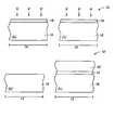
- FIG. 1shows a semiconductor wafer 10 at a preliminary processing step of the present invention.
- Wafer 10comprises a substrate 16 which is divided into a first region 12 and a second region 14 .
- Substrate 16can comprise, for example, monocrystalline silicon lightly doped with a background p-type dopant.
- the terms “semiconductive substrate” and “semiconductor substrate”are defined to mean any construction comprising semiconductive material, including, but not limited to, bulk semiconductive materials such as a semiconductive wafer (either alone or in assemblies comprising other materials thereon), and semiconductive material layers (either alone or in assemblies comprising other materials).
- substraterefers to any supporting structure, including, but not limited to, the semiconductive substrates described above.
- Regions 12 and 14can correspond to differently-doped regions of substrate 16 .
- region 12can correspond to a portion of substrate 16 having a heavier concentration of n-type conductivity enhancing dopant than p-type conductivity enhancing dopant, and can accordingly be referred to as an n-type doped region.
- region 14can correspond to a region of substrate 16 wherein the p-type dopant concentration is heavier than any n-type dopant concentration, and can accordingly be referred to as a p-type region of substrate 10 .
- substrate 16 of region 12is labeled with an “n”
- region 14is labeled with a “p”.
- regions 12 and 14corresponds to a particular embodiment of the present invention, and that other embodiments are encompassed wherein both of regions 12 and 14 are similarly doped, including embodiments wherein regions 12 and 14 are both heavier doped with n-type dopant than p-type dopant, as well as embodiments wherein regions 12 and 14 are both heavier doped with p-type dopant than n-type dopant.
- regions 12 and 14correspond to portions of a semiconductor memory assembly, and in such embodiments regions 12 and 14 can both correspond to memory array regions, or can both correspond to regions peripheral to a memory array regions, or alternatively one of regions 12 and 14 can correspond to a memory array region while the other regions 12 and 14 corresponds to a portion of the wafer peripheral to the memory array region.
- Oxide layer 18is formed over substrate 16 .
- Oxide layer 18can comprise, for example, silicon dioxide and can be formed by chemical vapor deposition over layer 16 .
- substrate 16comprises silicon (such as, for example, if substrate 16 is monocrystalline silicon)
- a silicon dioxide layer 18can be formed by oxidizing an upper surface of substrate 16 .
- Nitrogenis shown being dispersed onto and within layer 18 .
- the nitrogenis preferably formed primarily at a surface of oxide layer 18 .
- Layer 18is preferably less than 50 last 10 ⁇ above substrate 16 .
- substantially all of the nitrogen formed within layer 18is preferably at least 10 ⁇ above substrate 16 .
- the reference to “substantially all” of the nitrogen within silicon dioxide layer 18 being at least 10 ⁇ above substrate 16is defined to indicate that no measurable amount of nitrogen is in the portion of layer that is within 10 ⁇ of substrate 16 .
- substantially all of the nitrogen formed within layer 18is formed within the top 10 ⁇ of layer 18 . In other words, no measurable amount of nitrogen extends below the top 10 ⁇ of layer 18 , which can, in particular embodiments, indicate that an entirety of the nitrogen is within the top 10 ⁇ of layer 18 .
- FIGS. 8 and 9illustrate apparatuses which can be utilized for forming nitrogen within only the upper portions of silicon dioxide layer 18 .
- nitrogen-comprising region 22can be formed by remote plasma nitridization utilizing an apparatus 200 .
- Apparatus 200comprises a plasma chamber 202 and a reaction chamber 204 .
- Reaction chamber 204comprises a substrate holder 206 , and substrate 16 is supported within chamber 204 by holder 206 .
- holder 206is configured to rotate substrate 16 during exposure of substrate 16 to activated nitrogen species.
- Such activated nitrogen speciesare formed within plasma chamber 202 by, for example, exposing N 2 and/or other nitrogen-containing materials (such as N 2 O or NH 3 ) to plasma conditions, with the term “activated” indicating that the nitrogen species is different than the form of nitrogen fed to the plasma.
- An activated nitrogen speciescan comprise, for example, a nitrogen ion or a nitrogen atom in an energy state higher than its ground state.
- Exemplary plasma conditionscomprise utilization of a microwave plasma generator at a power of from about 1,500 watts to about 3,000 watts, and utilizing a pressure within chamber 202 of less than or equal to about 3 Torr.
- the plasma of chamber 202forms activated nitrogen species which migrate along a passageway 208 into chamber 204 whereupon the species can form a nitrogen-comprising layer over and within oxide 18 ( FIG. 1 ).
- passageway 208An arrow is shown within passageway 208 to indicate migration of plasma activated nitrogen species through passageway 208 .
- passageway 208is of sufficient length so that plasma 202 is at least about 12 inches from substrate 16 .
- substrate 16is preferably not biased relative to the plasma within chamber 202 .
- Suitable operating conditions for forming a nitrogen-comprising plasma over substrate 16can include maintaining a temperature of substrate 16 at from about 550° C. to about 1,000° C., rotating the wafer at about 90 rotations per minute (RPM), maintaining a pressure within chambers 202 and 204 of from about 0.8 Torr to about 2.8 Torr, and exposing the wafer to the nitridization conditions for from about one minute to about five minutes.
- RPMrotations per minute
- Apparatus 220can be referred to as a high density plasma remote plasma nitridization (HDP-RPN) apparatus, or simply as a plasma nitridization (PN) apparatus.
- Apparatus 220comprises a reaction chamber 222 having a wafer holder 224 therein. Wafer 16 is supported on holder 224 .
- a plasma 226is formed above substrate 16 , and preferably is maintained a distance “X” from substrate 16 , with distance “X” corresponding to at least about four inches.
- Nitrogenis introduced into plasma 226 in the form of, for example, N 2 , and activated nitrogen species are formed from the nitrogen.
- Suitable processing parameters for utilization of the apparatus of FIG. 9include a wafer temperature of from 0° C. to 400° C., no rotation of the substrate 16 , a pressure within chamber 222 of from about 5 mTorr to about 15 mTorr (preferably of from about 5 mTorr to about 10 mTorr), and an exposure time of substrate 16 to activated nitrogen species within chamber 222 of from about 5 seconds to about 30 seconds.
- a conductive layer 20is formed over oxide 18 , and a patterned masking layer 22 is formed over the portion of conductive layer 20 that is associated with region 12 , while the portion of conductive layer 20 associated with region 14 remains exposed.
- Conductive material 20can comprise, for example, conductively doped silicon, such as, for example, conductively doped amorphous or polycrystalline silicon.
- conductive layer 20comprises p-type doped silicon.
- Conductive material 20can also comprise metals, and/or silicides, in addition to, or alternatively to, the conductively doped silicon.
- Masking layer 22can comprise, for example, photoresist, and can be patterned by photolithographic processing.
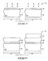
- wafer fragment 10is shown after being exposed to etching conditions which remove layers 20 and 18 from over region 14 of substrate 16 .
- Masking layer 22( FIG. 2 ) protects layers 18 and 20 from being removed over region 12 of substrate 16 .
- a suitable etchant for removing materials 18 and 20 from over substrate 16can comprise, for example, CF 4 and O 2 .
- region 14can be covered during formation of oxide layer 18 and conductive layer 20 , and subsequently the cover removed from over region 14 to form a structure identical to that shown in FIG. 3 .
- oxide layer 24is shown after being exposed to oxidizing conditions.
- the oxidizing conditionsform an oxide layer 24 over substrate 16 , and also form an oxide layer over conductive material 20 .
- substrate 16comprises monocrystalline silicon
- conductive material 20comprises conductively doped silicon
- oxide layers 24 and 26will comprise silicon dioxide.
- Oxide layers 24 and 26can be formed by methods other than oxidation of layer 20 and substrate 16 , such as, for example, by chemical vapor deposition of silicon dioxide.
- the inventionencompasses embodiments wherein oxide is not formed over layer 20 , such as, for example, embodiments in which oxide layer 24 is formed by oxidation of substrate 16 and in which layer 20 comprises a non-oxidizable material.
- Oxide layer 24can be formed to be a different thickness than oxide layer 18 .
- oxide layer 18can be optimized for formation of a PMOS transistor, and accordingly can be less than 50 ⁇ thick, and, for example, about 40 ⁇ thick, while oxide layer 24 can be optimized for formation of an NMOS transistor, and accordingly can be greater than 50 ⁇ thick, and, for example, can be about 70 ⁇ thick.
- Conductive material 28can comprise, for example, conductively doped silicon, and in particular embodiments comprises n-type doped silicon. Conductive material 28 can comprise other conductive materials in addition to, or alternatively to, conductively doped silicon, such as, for example, metals and/or silicides.
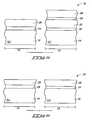
- planarizing conditionswhich planarize an upper surface of wafer 10 and remove layers 26 and 28 from over first conductive layer 20 .
- Exemplary planarizing conditionscomprise chemical-mechanical polishing.
- a polysilicon dry etchcan be utilized to remove polysilicon from over both of regions 12 and 14 .
- a suitable polysilicon dry etchis an isotropic etch utilizing HBr.
- layers 18 and 20are incorporated into a first transistor structure 40 and layers 24 and 28 are incorporated into a second transistor structure 42 .
- First transistor structure 40comprises a silicide layer 44 and an insulative layer 46 which are formed over layers 18 and 20 and patterned together with layers 18 and 20 to form a gate structure.
- Silicide layer 44can comprise, for example, titanium silicide or tungsten silicide.
- Second transistor structure 42comprises a silicide layer 48 and insulative layer 50 which are formed over layers 24 and 28 and patterned with layers 24 and 28 to form a gate structure.
- Silicide layer 48can comprise, for example, titanium silicide or tungsten silicide
- insulative layer 50can comprise, for example, silicon nitride.
- Spacers 52are shown formed along sidewalls of patterned materials 24 , 28 , 48 and 50 , as well as along sidewalls of patterned materials 18 , 20 , 44 and 46 .
- Spacers 52comprise insulative materials, and can comprise, for example, silicon dioxide or silicon nitride.
- conductive layers 44 and 48are shown separately from conductive materials 20 and 28 , silicides 44 and 48 could also have been incorporated into conductive materials 20 and 28 , respectively.
- conductive material 20could, in particular embodiments, encompass two layers, with a lower layer comprising conductively doped silicon and an upper layer comprising a silicide; and similarly conductive material 28 could, in particular embodiments, encompass two layers with a lower layer comprising conductively doped silicon and an upper layer comprising a silicide.
- Lightly doped diffusion (Ldd) regions 54are shown within region 12 of substrate 16 , and source/drain regions 56 are also shown within region 12 of substrate 16 .
- Source/drain regions 56comprise p-type dopant and together with Ldd regions 54 and layers 18 , 20 , 44 and 46 define a PMOS transistor 40 .
- Lightly doped diffusion regions 54typically comprise p-type dopant.
- Lightly doped diffusion regions 58are shown within region 14 of substrate 16 and heavily doped source/drain regions 60 are also shown within region 14 of substrate 16 .
- Heavily doped source/drain regions 60comprise n-type dopant, and together with layers 24 , 28 , 48 and 50 define NMOS transistor 42 .
- Lightly doped diffusion regions 58typically comprise n-type dopant.
Landscapes
- Metal-Oxide And Bipolar Metal-Oxide Semiconductor Integrated Circuits (AREA)
- Insulated Gate Type Field-Effect Transistor (AREA)
Abstract
Description
This application is a continuation of U.S. patent application Ser. No. 12/145,772, filed Jun. 25, 2008, now U.S. Pat. No. 7,803,678, which is a continuation of U.S. patent application Ser. No. 10/757,276, filed Jan. 14, 2004, now issued U.S. Pat. No. 7,399,714, which is a continuation of U.S. patent application Ser. No. 09/602,089, filed Jun. 22, 2000, now issued U.S. Pat. No. 6,686,298, entitled “Methods of Forming Structures over Semiconductor Substrates, and Methods of Forming Transistors Associated with Semiconductor Substrates”, naming Kevin L. Beaman and John T. Moore as inventors, the disclosures of which are hereby incorporated herein by reference.
The invention pertains to methods of forming structures over semiconductor substrates, and in particular embodiments pertains to methods of forming transistors associated with semiconductor substrates. The invention also pertains to semiconductor assemblies.
There are numerous applications in semiconductor processing in which it is desired to form conductive layers over oxides. For instance, transistor structures frequently comprise conductive layers formed over silicon dioxide (commonly referred to as a gate oxide). In some instances, the conductive materials comprise conductively doped silicon, and in such instances dopant can occasionally migrate through the oxide into an underlying substrate. In particular transistor devices, such dopant migration can be problematic. For instance, PMOS devices comprise an n-type channel region underneath a gate oxide, and can comprise p-type doped silicon over the gate oxide. If p-type dopant migrates from the silicon, through the oxide, and into the underlying substrate it will change the doping within the n-type channel. Such change can affect, and even destroy, electrical properties of the transistor. Accordingly, it can be desired to alleviate dopant migration relative to PMOS devices.
In contrast to the above-discussed problems which can be associated with PMOS devices, dopant migration is typically not problematic relative to NMOS devices. However, NMOS devices can have their own associated problems. For instance, it can be desired to form gate oxide for NMOS devices which is thicker than that utilized for PMOS devices. Such can be problematic in semiconductor wafer processing, in that both NMOS devices and PMOS devices are frequently formed over the same wafer. It would be desired to develop methodology which enables different gate oxide thicknesses to be associated with different transistors on the same wafer, and in particular applications desired to develop methodology to enable NMOS transistors to have thicker gate oxide than PMOS transistors.
In one aspect, the invention encompasses a method of forming a structure over a semiconductor substrate. A silicon dioxide containing layer is formed across at least some of the substrate. Nitrogen is formed within the silicon dioxide containing layer. Substantially all of the nitrogen within the silicon dioxide is at least 10 Å above the substrate. After the nitrogen is formed within the silicon dioxide layer, conductively doped silicon is formed on the silicon dioxide layer.
In another aspect, the invention encompasses a method of forming a pair of transistors associated with a semiconductor substrate. First and second regions of the substrate are defined. A first oxide region is formed to cover at least some of the first region of the substrate, and to not cover the second region of the substrate. Nitrogen is formed within the first oxide region. After the nitrogen is formed, a first conductive layer is formed over the first oxide region. The first conductive layer does not cover the second region of the substrate. After the first conductive layer is formed, a second oxide region is formed over the second region of the substrate. A second conductive layer is formed over the second oxide region. The first conductive layer is patterned into a first transistor gate, and the second conductive layer is patterned into a second transistor gate. First source/drain regions are formed proximate the first transistor gate, and the second source/drain regions are formed proximate the second transistor gate.
In other aspects, the invention pertains to semiconductor assemblies.
Preferred embodiments of the invention are described below with reference to the following accompanying drawings.
This disclosure of the invention is submitted in furtherance of the constitutional purposes of the U.S. Patent Laws “to promote the progress of science and useful arts” (Article 1, Section 8).
In particular embodiments of the present invention,regions such embodiments regions regions other regions
Anoxide layer 18 is formed oversubstrate 16.Oxide layer 18 can comprise, for example, silicon dioxide and can be formed by chemical vapor deposition overlayer 16. Alternatively, ifsubstrate 16 comprises silicon (such as, for example, ifsubstrate 16 is monocrystalline silicon) asilicon dioxide layer 18 can be formed by oxidizing an upper surface ofsubstrate 16.
Nitrogen is shown being dispersed onto and withinlayer 18. The nitrogen is preferably formed primarily at a surface ofoxide layer 18.Layer 18 is preferably less than 50 last 10 Å abovesubstrate 16. Alternatively, substantially all of the nitrogen formed withinlayer 18 is preferably at least 10 Å abovesubstrate 16. For purposes of interpreting this document and the claims that follow, it is to be understood that the reference to “substantially all” of the nitrogen withinsilicon dioxide layer 18 being at least 10 Å abovesubstrate 16 is defined to indicate that no measurable amount of nitrogen is in the portion of layer that is within 10 Å ofsubstrate 16. In particular embodiments of the present invention, substantially all of the nitrogen formed withinlayer 18 is formed within the top 10 Å oflayer 18. In other words, no measurable amount of nitrogen extends below the top 10 Å oflayer 18, which can, in particular embodiments, indicate that an entirety of the nitrogen is within the top 10 Å oflayer 18.
An arrow is shown withinpassageway 208 to indicate migration of plasma activated nitrogen species throughpassageway 208. Preferably,passageway 208 is of sufficient length so thatplasma 202 is at least about 12 inches fromsubstrate 16. Such can enable highly activated nitrogen species formed within a plasma to relax prior to interaction withsubstrate 16, which can limit penetration of the nitrogen species intosubstrate 16 relative to an amount of penetration which would occur with more highly activated species. In order to further limit penetration of nitrogen species intosubstrate 16,substrate 16 is preferably not biased relative to the plasma withinchamber 202.
Suitable operating conditions for forming a nitrogen-comprising plasma oversubstrate 16 can include maintaining a temperature ofsubstrate 16 at from about 550° C. to about 1,000° C., rotating the wafer at about 90 rotations per minute (RPM), maintaining a pressure withinchambers
An alternative apparatus which can be utilized for forming nitrogen over and within oxide layer18 (FIG. 1 ) is described with reference toFIG. 9 asapparatus 220.Apparatus 220 can be referred to as a high density plasma remote plasma nitridization (HDP-RPN) apparatus, or simply as a plasma nitridization (PN) apparatus.Apparatus 220 comprises areaction chamber 222 having awafer holder 224 therein.Wafer 16 is supported onholder 224. Aplasma 226 is formed abovesubstrate 16, and preferably is maintained a distance “X” fromsubstrate 16, with distance “X” corresponding to at least about four inches. Nitrogen is introduced intoplasma 226 in the form of, for example, N2, and activated nitrogen species are formed from the nitrogen. Suitable processing parameters for utilization of the apparatus ofFIG. 9 include a wafer temperature of from 0° C. to 400° C., no rotation of thesubstrate 16, a pressure withinchamber 222 of from about 5 mTorr to about 15 mTorr (preferably of from about 5 mTorr to about 10 mTorr), and an exposure time ofsubstrate 16 to activated nitrogen species withinchamber 222 of from about 5 seconds to about 30 seconds.
Referring next toFIG. 2 , aconductive layer 20 is formed overoxide 18, and apatterned masking layer 22 is formed over the portion ofconductive layer 20 that is associated withregion 12, while the portion ofconductive layer 20 associated withregion 14 remains exposed.
Maskinglayer 22 can comprise, for example, photoresist, and can be patterned by photolithographic processing.
Referring toFIG. 3 ,wafer fragment 10 is shown after being exposed to etching conditions which remove layers20 and18 from overregion 14 ofsubstrate 16. Masking layer22 (FIG. 2 ) protectslayers region 12 ofsubstrate 16. In embodiments in whichoxide 18 comprises silicon dioxide andconductive material 20 comprises conductively doped silicon, a suitable etchant for removingmaterials substrate 16 can comprise, for example, CF4and O2.
It is noted that the structure shown inFIG. 3 can be obtained through processing methods other than that shown inFIGS. 1-3 . For instance,region 14 can be covered during formation ofoxide layer 18 andconductive layer 20, and subsequently the cover removed from overregion 14 to form a structure identical to that shown inFIG. 3 .
Referring toFIG. 4 ,wafer 10 is shown after being exposed to oxidizing conditions. The oxidizing conditions form anoxide layer 24 oversubstrate 16, and also form an oxide layer overconductive material 20. Ifsubstrate 16 comprises monocrystalline silicon andconductive material 20 comprises conductively doped silicon, oxide layers24 and26 will comprise silicon dioxide. Oxide layers24 and26 can be formed by methods other than oxidation oflayer 20 andsubstrate 16, such as, for example, by chemical vapor deposition of silicon dioxide. Also, it is noted that the invention encompasses embodiments wherein oxide is not formed overlayer 20, such as, for example, embodiments in whichoxide layer 24 is formed by oxidation ofsubstrate 16 and in whichlayer 20 comprises a non-oxidizable material.
Referring toFIG. 5 , a secondconductive material 28 is formed overregions substrate 16.Conductive material 28 can comprise, for example, conductively doped silicon, and in particular embodiments comprises n-type doped silicon.Conductive material 28 can comprise other conductive materials in addition to, or alternatively to, conductively doped silicon, such as, for example, metals and/or silicides.
Referring toFIG. 6 ,wafer 10 is exposed to planarizing conditions which planarize an upper surface ofwafer 10 and removelayers conductive layer 20. Exemplary planarizing conditions comprise chemical-mechanical polishing. Alternatively or in combination with the chemical-mechanical polishing, a polysilicon dry etch can be utilized to remove polysilicon from over both ofregions
Referring toFIG. 7 , layers18 and20 are incorporated into afirst transistor structure 40 and layers24 and28 are incorporated into asecond transistor structure 42.
It is noted that althoughconductive layers conductive materials silicides conductive materials conductive material 20 could, in particular embodiments, encompass two layers, with a lower layer comprising conductively doped silicon and an upper layer comprising a silicide; and similarlyconductive material 28 could, in particular embodiments, encompass two layers with a lower layer comprising conductively doped silicon and an upper layer comprising a silicide.
Lightly doped diffusion (Ldd)regions 54 are shown withinregion 12 ofsubstrate 16, and source/drain regions 56 are also shown withinregion 12 ofsubstrate 16. Source/drain regions 56 comprise p-type dopant and together withLdd regions 54 and layers18,20,44 and46 define aPMOS transistor 40. Lightly dopeddiffusion regions 54 typically comprise p-type dopant.
Lightly dopeddiffusion regions 58 are shown withinregion 14 ofsubstrate 16 and heavily doped source/drain regions 60 are also shown withinregion 14 ofsubstrate 16. Heavily doped source/drain regions 60 comprise n-type dopant, and together withlayers NMOS transistor 42. Lightly dopeddiffusion regions 58 typically comprise n-type dopant.
In compliance with the statute, the invention has been described in language more or less specific as to structural and methodical features. It is to be understood, however, that the invention is not limited to the specific features shown and described, since the means herein disclosed comprise preferred forms of putting the invention into effect. The invention is, therefore, claimed in any of its forms or modifications within the proper scope of the appended claims appropriately interpreted in accordance with the doctrine of equivalents.
Claims (8)
1. A method of forming a structure over a semiconductor substrate, the method comprising:
providing the semiconductor substrate, the substrate comprising a first region and a second region, the first region comprising a differently-doped region than the second region;
forming a first oxide layer over the first and second regions;
exposing the first oxide layer to an activated nitrogen species formed from plasma conditions to provide nitrogen into at least a portion of the first oxide layer over the first region;
forming a first conductive layer over the first oxide layer and over the first and second regions;
forming a second oxide layer over the first and second regions;
forming a second conductive layer over the first and second regions; and
removing the first conductive layer from over the second region before the forming of the second oxide layer and the second conductive layer.
2. The method ofclaim 1 wherein the forming of the second oxide layer comprises forming the second oxide layer against the first conductive layer.
3. A method of forming a structure over a semiconductor substrate, the method comprising:
providing the semiconductor substrate, the substrate comprising a first region and a second region, the first region comprising a different area of the substrate than the second region;
providing a first oxide layer over the first region, the first oxide layer comprising a first thickness extending generally perpendicularly relative the substrate;
providing a second oxide layer over the second region, the second oxide layer comprising a second thickness extending generally perpendicularly relative the substrate, the second thickness being greater than the first thickness of the first oxide layer;
exposing the first oxide layer to an activated nitrogen species formed from plasma conditions to provide nitrogen into the first oxide layer; and
providing a conductive layer against the first and second oxide layers, the conductive layer comprising a thickness extending generally perpendicularly relative the substrate, the thickness of the conductive layer over the first region being substantially equal to the thickness of the conductive layer over the second region,
wherein the first oxide layer further comprises an upper portion and a lower portion, the upper portion comprising an upper surface and being spaced from the semiconductor substrate by the lower portion, and wherein the providing of the nitrogen comprises providing substantially all of the nitrogen within the upper portion.
4. A method of forming a structure over a semiconductor substrate, the method comprising:
providing the semiconductor substrate, the substrate comprising a first region and a second region, the first region comprising a different area of the substrate than the second region;
providing a first oxide layer over the first region, the first oxide layer comprising a first thickness extending generally perpendicularly relative the substrate;
providing a second oxide layer over the second region, the second oxide layer comprising a second thickness extending generally perpendicularly relative the substrate, the second thickness being greater than the first thickness of the first oxide layer;
exposing the first oxide layer to an activated nitrogen species formed from plasma conditions to provide nitrogen into the first oxide layer; and
providing a conductive layer against the first and second oxide layers, the conductive layer comprising a thickness extending generally perpendicularly relative the substrate, the thickness of the conductive layer over the first region being substantially equal to the thickness of the conductive layer over the second region,
wherein the first oxide layer further comprises an upper portion and a lower portion, the upper portion comprising an upper surface and being spaced from the semiconductor substrate by the lower portion, and wherein the providing of the nitrogen comprises no measurable amount of the nitrogen within the lower portion.
5. The method ofclaim 4 wherein the lower portion of the first oxide layer comprises a thickness of about 10 angstroms.
6. The method ofclaim 4 , wherein the upper portion of the first oxide layer comprises a thickness of about 10 angstroms.
7. A method of forming a structure over a semiconductor substrate, the method comprising:
providing the semiconductor substrate, the substrate comprising a first region and a second region, the first region comprising a different area of the substrate than the second region;
providing a first oxide layer over the first region, the first oxide layer comprising a first thickness extending generally perpendicularly relative the substrate;
providing a second oxide layer over the second region, the second oxide layer comprising a second thickness extending generally perpendicularly relative the substrate, the second thickness being greater than the first thickness of the first oxide layer;
exposing the first oxide layer to an activated nitrogen species formed from plasma conditions to provide nitrogen into the first oxide layer; and
providing a conductive layer against the first and second oxide layers, the conductive layer comprising a thickness extending generally perpendicularly relative the substrate, the thickness of the conductive layer over the first region being substantially equal to the thickness of the conductive layer over the second region,
wherein the providing of the nitrogen comprises:
forming an activated nitrogen species comprising a first energy state,
changing the first energy state of the activated nitrogen species to a second energy state that is different from the first energy state, and
exposing the first oxide layer to the activated nitrogen species at the second energy state.
8. The method ofclaim 7 wherein the second energy state is a energy state than the first energy state.
Priority Applications (1)
| Application Number | Priority Date | Filing Date | Title |
|---|---|---|---|
| US12/803,296US8017470B2 (en) | 2000-06-22 | 2010-06-23 | Method of forming a structure over a semiconductor substrate |
Applications Claiming Priority (4)
| Application Number | Priority Date | Filing Date | Title |
|---|---|---|---|
| US09/602,089US6686298B1 (en) | 2000-06-22 | 2000-06-22 | Methods of forming structures over semiconductor substrates, and methods of forming transistors associated with semiconductor substrates |
| US10/757,276US7399714B2 (en) | 2000-06-22 | 2004-01-14 | Method of forming a structure over a semiconductor substrate |
| US12/145,772US7803678B2 (en) | 2000-06-22 | 2008-06-25 | Method of forming a structure over a semiconductor substrate |
| US12/803,296US8017470B2 (en) | 2000-06-22 | 2010-06-23 | Method of forming a structure over a semiconductor substrate |
Related Parent Applications (1)
| Application Number | Title | Priority Date | Filing Date |
|---|---|---|---|
| US12/145,772ContinuationUS7803678B2 (en) | 2000-06-22 | 2008-06-25 | Method of forming a structure over a semiconductor substrate |
Publications (2)
| Publication Number | Publication Date |
|---|---|
| US20100267226A1 US20100267226A1 (en) | 2010-10-21 |
| US8017470B2true US8017470B2 (en) | 2011-09-13 |
Family
ID=24409918
Family Applications (6)
| Application Number | Title | Priority Date | Filing Date |
|---|---|---|---|
| US09/602,089Expired - LifetimeUS6686298B1 (en) | 2000-06-22 | 2000-06-22 | Methods of forming structures over semiconductor substrates, and methods of forming transistors associated with semiconductor substrates |
| US09/993,109Expired - LifetimeUS6690046B2 (en) | 2000-06-22 | 2001-11-13 | Semiconductor assemblies, methods of forming structures over semiconductor substrates, and methods of forming transistors associated with semiconductor substrates |
| US10/757,276Expired - Fee RelatedUS7399714B2 (en) | 2000-06-22 | 2004-01-14 | Method of forming a structure over a semiconductor substrate |
| US11/217,775Expired - Fee RelatedUS7371647B2 (en) | 2000-06-22 | 2005-09-01 | Methods of forming transistors |
| US12/145,772Expired - Fee RelatedUS7803678B2 (en) | 2000-06-22 | 2008-06-25 | Method of forming a structure over a semiconductor substrate |
| US12/803,296Expired - Fee RelatedUS8017470B2 (en) | 2000-06-22 | 2010-06-23 | Method of forming a structure over a semiconductor substrate |
Family Applications Before (5)
| Application Number | Title | Priority Date | Filing Date |
|---|---|---|---|
| US09/602,089Expired - LifetimeUS6686298B1 (en) | 2000-06-22 | 2000-06-22 | Methods of forming structures over semiconductor substrates, and methods of forming transistors associated with semiconductor substrates |
| US09/993,109Expired - LifetimeUS6690046B2 (en) | 2000-06-22 | 2001-11-13 | Semiconductor assemblies, methods of forming structures over semiconductor substrates, and methods of forming transistors associated with semiconductor substrates |
| US10/757,276Expired - Fee RelatedUS7399714B2 (en) | 2000-06-22 | 2004-01-14 | Method of forming a structure over a semiconductor substrate |
| US11/217,775Expired - Fee RelatedUS7371647B2 (en) | 2000-06-22 | 2005-09-01 | Methods of forming transistors |
| US12/145,772Expired - Fee RelatedUS7803678B2 (en) | 2000-06-22 | 2008-06-25 | Method of forming a structure over a semiconductor substrate |
Country Status (1)
| Country | Link |
|---|---|
| US (6) | US6686298B1 (en) |
Families Citing this family (19)
| Publication number | Priority date | Publication date | Assignee | Title |
|---|---|---|---|---|
| US6686298B1 (en)* | 2000-06-22 | 2004-02-03 | Micron Technology, Inc. | Methods of forming structures over semiconductor substrates, and methods of forming transistors associated with semiconductor substrates |
| US6660657B1 (en) | 2000-08-07 | 2003-12-09 | Micron Technology, Inc. | Methods of incorporating nitrogen into silicon-oxide-containing layers |
| TW531803B (en)* | 2000-08-31 | 2003-05-11 | Agere Syst Guardian Corp | Electronic circuit structure with improved dielectric properties |
| US6878585B2 (en)* | 2001-08-29 | 2005-04-12 | Micron Technology, Inc. | Methods of forming capacitors |
| KR20030044394A (en)* | 2001-11-29 | 2003-06-09 | 주식회사 하이닉스반도체 | Method for fabricating semiconductor device with dual gate dielectric layer |
| US6723599B2 (en)* | 2001-12-03 | 2004-04-20 | Micron Technology, Inc. | Methods of forming capacitors and methods of forming capacitor dielectric layers |
| US7138691B2 (en)* | 2004-01-22 | 2006-11-21 | International Business Machines Corporation | Selective nitridation of gate oxides |
| JP4040602B2 (en)* | 2004-05-14 | 2008-01-30 | Necエレクトロニクス株式会社 | Semiconductor device |
| KR100668954B1 (en)* | 2004-12-15 | 2007-01-12 | 동부일렉트로닉스 주식회사 | Method of manufacturing thin film transistor |
| JP2007288096A (en)* | 2006-04-20 | 2007-11-01 | Matsushita Electric Ind Co Ltd | Semiconductor device and manufacturing method thereof |
| EP2053652A1 (en)* | 2007-06-15 | 2009-04-29 | Stmicroelectronics Sa | Process for manufacturing field effect transistors |
| US7928020B2 (en)* | 2007-09-27 | 2011-04-19 | Chartered Semiconductor Manufacturing Ltd. | Method of fabricating a nitrogenated silicon oxide layer and MOS device having same |
| FI122216B (en)* | 2009-01-05 | 2011-10-14 | Imbera Electronics Oy | Rigid-flex module |
| US9412640B2 (en) | 2013-01-25 | 2016-08-09 | GlobalFoundries, Inc. | Semiconductor device including substrate contact and related method |
| KR102494614B1 (en)* | 2015-03-20 | 2023-02-02 | 어플라이드 머티어리얼스, 인코포레이티드 | Atomic layer process chamber for 3D conformal processing |
| US10320948B2 (en)* | 2015-11-30 | 2019-06-11 | Successfactors, Inc. | Application footprint recorder and synchronizer |
| WO2019089916A1 (en)* | 2017-11-01 | 2019-05-09 | The Charles Stark Draper Laboratory, Inc. | Integrated process flow for semiconductor devices |
| JP2021044519A (en) | 2019-09-13 | 2021-03-18 | キオクシア株式会社 | Semiconductor device |
| US11411081B2 (en) | 2020-04-22 | 2022-08-09 | Globalfoundries U.S. Inc. | Field effect transistor (FET) stack and methods to form same |
Citations (150)
| Publication number | Priority date | Publication date | Assignee | Title |
|---|---|---|---|---|
| US3627598A (en) | 1970-02-05 | 1971-12-14 | Fairchild Camera Instr Co | Nitride passivation of mesa transistors by phosphovapox lifting |
| US4254161A (en) | 1979-08-16 | 1981-03-03 | International Business Machines Corporation | Prevention of low pressure chemical vapor deposition silicon dioxide undercutting and flaking |
| US4262631A (en) | 1979-10-01 | 1981-04-21 | Kubacki Ronald M | Thin film deposition apparatus using an RF glow discharge |
| US4435447A (en) | 1978-12-26 | 1984-03-06 | Fujitsu Limited | Method for forming an insulating film on a semiconductor substrate surface |
| US4605447A (en) | 1983-05-16 | 1986-08-12 | U.S. Philips Corporation | Methods of manufacturing semiconductor devices |
| US4882649A (en) | 1988-03-29 | 1989-11-21 | Texas Instruments Incorporated | Nitride/oxide/nitride capacitor dielectric |
| US4891684A (en) | 1986-08-04 | 1990-01-02 | Hitachi, Ltd. | Semiconductor device |
| US4980307A (en) | 1978-06-14 | 1990-12-25 | Fujitsu Limited | Process for producing a semiconductor device having a silicon oxynitride insulative film |
| US4996081A (en) | 1985-01-21 | 1991-02-26 | Ellul Joseph P | Method of forming multiple nitride coating on silicon |
| US5026574A (en) | 1986-03-19 | 1991-06-25 | The General Electric Company, P.L.C. | Chemical vapor deposition process for depositing large-grain polysilicon films |
| US5032545A (en) | 1990-10-30 | 1991-07-16 | Micron Technology, Inc. | Process for preventing a native oxide from forming on the surface of a semiconductor material and integrated circuit capacitors produced thereby |
| US5051794A (en) | 1988-07-05 | 1991-09-24 | Kabushiki Kaisha Toshiba | Non-volatile semiconductor memory device and method for manufacturing the same |
| US5142438A (en) | 1991-11-15 | 1992-08-25 | Micron Technology, Inc. | Dram cell having a stacked capacitor with a tantalum lower plate, a tantalum oxide dielectric layer, and a silicide buried contact |
| US5164331A (en) | 1991-10-03 | 1992-11-17 | Hewlett-Packard Company | Method of forming and etching titanium-tungsten interconnects |
| US5227651A (en) | 1991-03-23 | 1993-07-13 | Samsung Electronics, Co., Ltd. | Semiconductor device having a capacitor with an electrode grown through pinholes |
| US5237188A (en) | 1990-11-28 | 1993-08-17 | Kabushiki Kaisha Toshiba | Semiconductor device with nitrided gate insulating film |
| US5254489A (en)* | 1990-10-18 | 1993-10-19 | Nec Corporation | Method of manufacturing semiconductor device by forming first and second oxide films by use of nitridation |
| US5258333A (en) | 1992-08-18 | 1993-11-02 | Intel Corporation | Composite dielectric for a semiconductor device and method of fabrication |
| US5318924A (en) | 1991-10-03 | 1994-06-07 | Hewlett-Packard Company | Nitridation of titanium-tungsten interconnects |
| US5324679A (en) | 1991-03-23 | 1994-06-28 | Samsung Electronics Co., Ltd. | Method for manufacturing a semiconductor device having increased surface area conductive layer |
| US5330936A (en) | 1991-05-27 | 1994-07-19 | Nec Corporation | Method of producing a silicon nitride film and method of fabricating a semiconductor device |
| US5330920A (en) | 1993-06-15 | 1994-07-19 | Digital Equipment Corporation | Method of controlling gate oxide thickness in the fabrication of semiconductor devices |
| US5334554A (en) | 1992-01-24 | 1994-08-02 | Taiwan Semiconductor Manufacturing Co., Ltd. | Nitrogen plasma treatment to prevent field device leakage in VLSI processing |
| US5350707A (en) | 1991-11-19 | 1994-09-27 | Samsung Electronics Co., Ltd. | Method for making a capacitor having an electrode surface with a plurality of trenches formed therein |
| US5376593A (en) | 1992-12-31 | 1994-12-27 | Micron Semiconductor, Inc. | Method for fabricating stacked layer Si3 N4 for low leakage high capacitance films using rapid thermal nitridation |
| US5378645A (en) | 1992-05-21 | 1995-01-03 | Oki Electric Industry Co., Ltd. | Method of making a semiconductor device with a capacitor |
| US5382533A (en) | 1993-06-18 | 1995-01-17 | Micron Semiconductor, Inc. | Method of manufacturing small geometry MOS field-effect transistors having improved barrier layer to hot electron injection |
| US5393702A (en) | 1993-07-06 | 1995-02-28 | United Microelectronics Corporation | Via sidewall SOG nitridation for via filling |
| US5397748A (en) | 1991-12-28 | 1995-03-14 | Nec Corporation | Method of producing semiconductor device with insulating film having at least silicon nitride film |
| US5398641A (en) | 1993-07-27 | 1995-03-21 | Texas Instruments Incorporated | Method for p-type doping of semiconductor structures formed of group II and group VI elements |
| US5398647A (en) | 1994-02-16 | 1995-03-21 | Rivera; Efrain | Combined sleeve/poppet valve for internal combustion engine |
| US5436481A (en) | 1993-01-21 | 1995-07-25 | Nippon Steel Corporation | MOS-type semiconductor device and method of making the same |
| US5445999A (en) | 1992-11-13 | 1995-08-29 | Micron Technology, Inc. | Advanced technique to improve the bonding arrangement on silicon surfaces to promote uniform nitridation |
| US5449631A (en) | 1994-07-29 | 1995-09-12 | International Business Machines Corporation | Prevention of agglomeration and inversion in a semiconductor salicide process |
| US5459105A (en) | 1990-10-30 | 1995-10-17 | Mitsubishi Denki Kabushiki Kaisha | Method of manufacturing a semiconductor device having multilayer insulating films |
| US5464792A (en) | 1993-06-07 | 1995-11-07 | Motorola, Inc. | Process to incorporate nitrogen at an interface of a dielectric layer in a semiconductor device |
| US5498890A (en) | 1989-11-08 | 1996-03-12 | Samsung Electronics Co., Ltd. | Semiconductor device having a multi-layered dielectric structure and manufacturing method thereof |
| US5500380A (en) | 1993-04-16 | 1996-03-19 | Goldstar Co., Ltd. | Method for fabricating thin film transistor |
| US5504029A (en) | 1987-09-19 | 1996-04-02 | Hitachi, Ltd. | Method of producing semiconductor integrated circuit device having memory cell and peripheral circuit MISFETs |
| US5508542A (en) | 1994-10-28 | 1996-04-16 | International Business Machines Corporation | Porous silicon trench and capacitor structures |
| US5518946A (en) | 1991-10-07 | 1996-05-21 | Sony Corporation | Process for fabricating capacitors in dynamic RAM |
| US5518958A (en) | 1994-07-29 | 1996-05-21 | International Business Machines Corporation | Prevention of agglomeration and inversion in a semiconductor polycide process |
| US5523596A (en) | 1990-10-05 | 1996-06-04 | Mitsubishi Denki Kabushiki Kaisha | Semiconductor device having capacitor and manufacturing method therefor |
| WO1996039713A1 (en) | 1995-06-06 | 1996-12-12 | Advanced Micro Devices, Inc. | A method of forming high pressure silicon oxynitride (oxynitride) gate dielectrics for metal oxide semiconductor (mos) devices with p+ polycrystalline silicon (polysilicon) gate electrodes |
| US5596218A (en) | 1993-10-18 | 1997-01-21 | Digital Equipment Corporation | Hot carrier-hard gate oxides by nitrogen implantation before gate oxidation |
| US5612558A (en) | 1995-11-15 | 1997-03-18 | Micron Technology, Inc. | Hemispherical grained silicon on refractory metal nitride |
| US5619057A (en) | 1994-01-19 | 1997-04-08 | Sony Corporation | Complex film overlying a substrate with defined work function |
| US5620908A (en) | 1994-09-19 | 1997-04-15 | Kabushiki Kaisha Toshiba | Manufacturing method of semiconductor device comprising BiCMOS transistor |
| US5633036A (en) | 1995-04-21 | 1997-05-27 | The Board Of Trustees Of The University Of Illinois | Selective low temperature chemical vapor deposition of titanium disilicide onto silicon regions |
| US5663077A (en) | 1993-07-27 | 1997-09-02 | Semiconductor Energy Laboratory Co., Ltd. | Method of manufacturing a thin film transistor in which the gate insulator comprises two oxide films |
| US5663036A (en) | 1994-12-13 | 1997-09-02 | International Business Machines Corporation | Microlithographic structure with an underlayer film comprising a thermolyzed azide |
| US5685949A (en) | 1995-01-13 | 1997-11-11 | Seiko Epson Corporation | Plasma treatment apparatus and method |
| US5716864A (en) | 1994-07-22 | 1998-02-10 | Nkk Corporation | Method of manufacturing a non-volatile semiconductor memory device with peripheral transistor |
| US5731235A (en) | 1996-10-30 | 1998-03-24 | Micron Technology, Inc. | Methods of forming a silicon nitrite film, a capacitor dielectric layer and a capacitor |
| US5760475A (en) | 1987-03-30 | 1998-06-02 | International Business Machines Corporation | Refractory metal-titanium nitride conductive structures |
| US5763922A (en) | 1997-02-28 | 1998-06-09 | Intel Corporation | CMOS integrated circuit having PMOS and NMOS devices with different gate dielectric layers |
| US5821142A (en) | 1996-04-08 | 1998-10-13 | Vanguard International Semiconductor | Method for forming a capacitor with a multiple pillar structure |
| US5834372A (en) | 1995-07-24 | 1998-11-10 | Lg Semicon., Ltd. | Pretreatment of semiconductor substrate |
| US5837592A (en) | 1995-12-07 | 1998-11-17 | Taiwan Semiconductor Manufacturing Company, Ltd. | Method for stabilizing polysilicon resistors |
| US5837598A (en) | 1997-03-13 | 1998-11-17 | Lsi Logic Corporation | Diffusion barrier for polysilicon gate electrode of MOS device in integrated circuit structure, and method of making same |
| US5840610A (en) | 1997-01-16 | 1998-11-24 | Advanced Micro Devices, Inc. | Enhanced oxynitride gate dielectrics using NF3 gas |
| US5844771A (en) | 1996-06-26 | 1998-12-01 | Micron Technology, Inc. | Capacitor construction |
| US5851603A (en) | 1997-07-14 | 1998-12-22 | Vanguard International Semiconductor Corporation | Method for making a plasma-enhanced chemical vapor deposited SiO2 Si3 N4 multilayer passivation layer for semiconductor applications |
| EP0886308A2 (en) | 1997-06-20 | 1998-12-23 | Japan Science and Technology Corporation | Plasma nitridation of a silicon oxide film |
| US5861651A (en) | 1997-02-28 | 1999-01-19 | Lucent Technologies Inc. | Field effect devices and capacitors with improved thin film dielectrics and method for making same |
| US5885877A (en) | 1997-04-21 | 1999-03-23 | Advanced Micro Devices, Inc. | Composite gate electrode incorporating dopant diffusion-retarding barrier layer adjacent to underlying gate dielectric |
| US5897354A (en) | 1996-12-17 | 1999-04-27 | Cypress Semiconductor Corporation | Method of forming a non-volatile memory device with ramped tunnel dielectric layer |
| US5920779A (en) | 1997-05-21 | 1999-07-06 | United Microelectronics Corp. | Differential gate oxide thickness by nitrogen implantation for mixed mode and embedded VLSI circuits |
| US5939750A (en) | 1998-01-21 | 1999-08-17 | Advanced Micro Devices | Use of implanted ions to reduce oxide-nitride-oxide (ONO) etch residue and polystringers |
| US5960289A (en) | 1998-06-22 | 1999-09-28 | Motorola, Inc. | Method for making a dual-thickness gate oxide layer using a nitride/oxide composite region |
| US5960302A (en) | 1996-12-31 | 1999-09-28 | Lucent Technologies, Inc. | Method of making a dielectric for an integrated circuit |
| US5969397A (en) | 1996-11-26 | 1999-10-19 | Texas Instruments Incorporated | Low defect density composite dielectric |
| US5970345A (en) | 1997-10-22 | 1999-10-19 | Texas Instruments Incorporated | Method of forming an integrated circuit having both low voltage and high voltage MOS transistors |
| US5972783A (en) | 1996-02-07 | 1999-10-26 | Matsushita Electric Industrial Co., Ltd. | Method for fabricating a semiconductor device having a nitrogen diffusion layer |
| US5972800A (en) | 1995-05-10 | 1999-10-26 | Nec Corporation | Method for fabricating a semiconductor device with multi-level structured insulator |
| US5981366A (en) | 1991-09-19 | 1999-11-09 | Sharp Kabushiki Kaisha | Method for manufacturing non-volatile memory |
| US5994749A (en) | 1997-01-20 | 1999-11-30 | Nec Corporation | Semiconductor device having a gate electrode film containing nitrogen |
| US5998253A (en) | 1997-09-29 | 1999-12-07 | Siemens Aktiengesellschaft | Method of forming a dopant outdiffusion control structure including selectively grown silicon nitride in a trench capacitor of a DRAM cell |
| US6001741A (en) | 1998-04-15 | 1999-12-14 | Lucent Technologies Inc. | Method for making field effect devices and capacitors with improved thin film dielectrics and resulting devices |
| US6001748A (en) | 1996-06-04 | 1999-12-14 | Sumitomo Electric Industries, Ltd. | Single crystal of nitride and process for preparing the same |
| US6008104A (en) | 1998-04-06 | 1999-12-28 | Siemens Aktiengesellschaft | Method of fabricating a trench capacitor with a deposited isolation collar |
| US6015739A (en) | 1997-10-29 | 2000-01-18 | Advanced Micro Devices | Method of making gate dielectric for sub-half micron MOS transistors including a graded dielectric constant |
| US6033998A (en) | 1998-03-09 | 2000-03-07 | Lsi Logic Corporation | Method of forming variable thickness gate dielectrics |
| US6040249A (en) | 1996-08-12 | 2000-03-21 | Texas Instruments Incorporated | Method of improving diffusion barrier properties of gate oxides by applying ions or free radicals of nitrogen in low energy |
| US6051865A (en) | 1998-11-09 | 2000-04-18 | Advanced Micro Devices, Inc. | Transistor having a barrier layer below a high permittivity gate dielectric |
| US6054396A (en) | 1996-05-09 | 2000-04-25 | Micron Technology, Inc. | Semiconductor processing method of reducing thickness depletion of a silicide layer at a junction of different underlying layers |
| US6057200A (en) | 1995-10-16 | 2000-05-02 | Micron Technology, Inc. | Method of making a field effect transistor having an elevated source and an elevated drain |
| US6057220A (en) | 1997-09-23 | 2000-05-02 | International Business Machines Corporation | Titanium polycide stabilization with a porous barrier |
| US6057584A (en) | 1997-12-19 | 2000-05-02 | Advanced Micro Devices, Inc. | Semiconductor device having a tri-layer gate insulating dielectric |
| US6060406A (en) | 1998-05-28 | 2000-05-09 | Lucent Technologies Inc. | MOS transistors with improved gate dielectrics |
| US6063713A (en) | 1997-11-10 | 2000-05-16 | Micron Technology, Inc. | Methods for forming silicon nitride layers on silicon-comprising substrates |
| US6080682A (en) | 1997-12-18 | 2000-06-27 | Advanced Micro Devices, Inc. | Methodology for achieving dual gate oxide thicknesses |
| US6080629A (en) | 1997-04-21 | 2000-06-27 | Advanced Micro Devices, Inc. | Ion implantation into a gate electrode layer using an implant profile displacement layer |
| US6087229A (en) | 1998-03-09 | 2000-07-11 | Lsi Logic Corporation | Composite semiconductor gate dielectrics |
| US6087236A (en) | 1998-11-24 | 2000-07-11 | Intel Corporation | Integrated circuit with multiple gate dielectric structures |
| US6091110A (en) | 1998-03-30 | 2000-07-18 | Spectrian Corporation | MOSFET device having recessed gate-drain shield and method |
| US6091109A (en) | 1998-05-11 | 2000-07-18 | Nec Corporation | Semiconductor device having different gate oxide thicknesses by implanting halogens in one region and nitrogen in the second region |
| US6093661A (en)* | 1999-08-30 | 2000-07-25 | Micron Technology, Inc. | Integrated circuitry and semiconductor processing method of forming field effect transistors |
| US6096597A (en) | 1997-01-31 | 2000-08-01 | Texas Instruments Incorporated | Method for fabricating an integrated circuit structure |
| US6100163A (en) | 1999-01-07 | 2000-08-08 | Taiwan Semiconductor Manufacturing Company | Gap filling of shallow trench isolation by ozone-tetraethoxysilane |
| US6110842A (en) | 1996-06-07 | 2000-08-29 | Texas Instruments Incorporated | Method of forming multiple gate oxide thicknesses using high density plasma nitridation |
| US6110780A (en) | 1999-04-01 | 2000-08-29 | Taiwan Semiconductor Manufacturing Company | Using NO or N2 O treatment to generate different oxide thicknesses in one oxidation step for single poly non-volatile memory |
| US6114203A (en)* | 1995-05-10 | 2000-09-05 | Stmicroelectronics S.R.L. | Method of manufacturing a MOS integrated circuit having components with different dielectrics |
| US6136636A (en) | 1998-03-25 | 2000-10-24 | Texas Instruments - Acer Incorporated | Method of manufacturing deep sub-micron CMOS transistors |
| US6140187A (en) | 1998-12-02 | 2000-10-31 | Lucent Technologies Inc. | Process for forming metal oxide semiconductors including an in situ furnace gate stack with varying silicon nitride deposition rate |
| US6146948A (en) | 1997-06-03 | 2000-11-14 | Motorola Inc. | Method for manufacturing a thin oxide for use in semiconductor integrated circuits |
| US6150226A (en) | 1998-02-03 | 2000-11-21 | Micron Technology, Inc. | Semiconductor processing methods, methods of forming capacitors, methods of forming silicon nitride, and methods of densifying silicon nitride layers |
| US6168980B1 (en) | 1992-08-27 | 2001-01-02 | Semiconductor Energy Laboratory Co., Ltd. | Semiconductor device and method for forming the same |
| US6171900B1 (en) | 1999-04-15 | 2001-01-09 | Taiwan Semiconductor Manufacturing Company | CVD Ta2O5/oxynitride stacked gate insulator with TiN gate electrode for sub-quarter micron MOSFET |
| US6184110B1 (en) | 1998-04-30 | 2001-02-06 | Sharp Laboratories Of America, Inc. | Method of forming nitrogen implanted ultrathin gate oxide for dual gate CMOS devices |
| US6197701B1 (en) | 1998-10-23 | 2001-03-06 | Taiwan Semiconductor Manufacturing Company | Lightly nitridation surface for preparing thin-gate oxides |
| US6201303B1 (en) | 1999-10-14 | 2001-03-13 | Advanced Micro Devices, Inc. | Method of forming a local interconnect with improved etch selectivity of silicon dioxide/silicide |
| US6207985B1 (en) | 1998-02-02 | 2001-03-27 | Texas Instruments Incorporated | DRAM memory cell and array having pass transistors with surrounding gate |
| US6207532B1 (en) | 1999-09-30 | 2001-03-27 | Taiwan Semiconductor Manufacturing Company | STI process for improving isolation for deep sub-micron application |
| US6207586B1 (en) | 1998-10-28 | 2001-03-27 | Lucent Technologies Inc. | Oxide/nitride stacked gate dielectric and associated methods |
| US6225167B1 (en) | 2000-03-13 | 2001-05-01 | Taiwan Semiconductor Manufacturing Company | Method of generating multiple oxide thicknesses by one oxidation step using NH3 nitridation followed by re-oxidation |
| US6228701B1 (en) | 1997-12-19 | 2001-05-08 | Seimens Aktiengesellschaft | Apparatus and method for minimizing diffusion in stacked capacitors formed on silicon plugs |
| US6245616B1 (en) | 1999-01-06 | 2001-06-12 | International Business Machines Corporation | Method of forming oxynitride gate dielectric |
| US6255703B1 (en) | 1999-06-02 | 2001-07-03 | Advanced Micro Devices, Inc. | Device with lower LDD resistance |
| US6268296B1 (en) | 1997-12-31 | 2001-07-31 | Texas Instruments Incorporated | Low temperature process for multiple voltage devices |
| US6274442B1 (en) | 1998-07-15 | 2001-08-14 | Advanced Micro Devices, Inc. | Transistor having a nitrogen incorporated epitaxially grown gate dielectric and method of making same |
| JP2001237243A (en) | 1999-12-23 | 2001-08-31 | Asm America Inc | Method and process for manufacturing in-situ dielectric stack |
| US6297162B1 (en) | 1999-09-27 | 2001-10-02 | Taiwan Semiconductor Manufacturing Company | Method to reduce silicon oxynitride etch rate in a silicon oxide dry etch |
| US20010036752A1 (en) | 1997-02-27 | 2001-11-01 | Scott J. Deboer | Methods and apparatus for forming a high dielectric film and the dielectric film formed thereby |
| US6323114B1 (en) | 1998-11-24 | 2001-11-27 | Texas Instruments Incorporated | Stacked/composite gate dielectric which incorporates nitrogen at an interface |
| US6331492B2 (en) | 1997-12-31 | 2001-12-18 | Texas Instruments Incorporated | Nitridation for split gate multiple voltage devices |
| US20020009861A1 (en) | 1998-06-12 | 2002-01-24 | Pravin K. Narwankar | Method and apparatus for the formation of dielectric layers |
| US6350707B1 (en) | 1999-09-03 | 2002-02-26 | United Microelectronics Corp. | Method of fabricating capacitor dielectric |
| US6362085B1 (en) | 2000-07-19 | 2002-03-26 | Taiwan Semiconductor Manufacturing Company | Method for reducing gate oxide effective thickness and leakage current |
| US6393981B1 (en) | 1998-12-09 | 2002-05-28 | Robert Cameron | Multiple color printer having vertically moveable print pad |
| US6399520B1 (en) | 1999-03-10 | 2002-06-04 | Tokyo Electron Limited | Semiconductor manufacturing method and semiconductor manufacturing apparatus |
| US6399448B1 (en) | 1999-11-19 | 2002-06-04 | Chartered Semiconductor Manufacturing Ltd. | Method for forming dual gate oxide |
| US6399445B1 (en) | 1997-12-18 | 2002-06-04 | Texas Instruments Incorporated | Fabrication technique for controlled incorporation of nitrogen in gate dielectric |
| US6410991B1 (en) | 1998-06-15 | 2002-06-25 | Mitsubishi Denki Kabushiki Kaisha | Semiconductor device and method of manufacturing the same |
| US6413881B1 (en) | 2000-03-09 | 2002-07-02 | Lsi Logic Corporation | Process for forming thin gate oxide with enhanced reliability by nitridation of upper surface of gate of oxide to form barrier of nitrogen atoms in upper surface region of gate oxide, and resulting product |
| US20020094620A1 (en) | 2000-08-07 | 2002-07-18 | Sandhu Gurtej S. | Transistor Structures |
| US6436771B1 (en) | 2001-07-12 | 2002-08-20 | Taiwan Semiconductor Manufacturing Company | Method of forming a semiconductor device with multiple thickness gate dielectric layers |
| US6450116B1 (en) | 1999-04-22 | 2002-09-17 | Applied Materials, Inc. | Apparatus for exposing a substrate to plasma radicals |
| US6482690B2 (en) | 1998-12-08 | 2002-11-19 | Matsushita Electric Industrial Co., Ltd. | Method for fabricating semiconductor device |
| US6492690B2 (en) | 1997-03-05 | 2002-12-10 | Mitsubishi Denki Kabushiki Kaisha | Semiconductor device having control electrodes with different impurity concentrations |
| US20030034518A1 (en) | 1999-03-08 | 2003-02-20 | Kabushiki Kaisha Toshiba | Method for manufacturing semiconductor memory |
| WO2003049159A2 (en) | 2001-12-03 | 2003-06-12 | Micron Technology, Inc. | Methods of forming capacitors and methods of forming capacitor dielectric layers |
| US6649543B1 (en) | 2000-06-22 | 2003-11-18 | Micron Technology, Inc. | Methods of forming silicon nitride, methods of forming transistor devices, and transistor devices |
| US6649538B1 (en) | 2002-10-09 | 2003-11-18 | Taiwan Semiconductor Manufacturing Co. Ltd. | Method for plasma treating and plasma nitriding gate oxides |
| US6653184B2 (en) | 2000-06-22 | 2003-11-25 | Micron Technology, Inc. | Method of forming transistors associated with semiconductor substrates comprising forming a nitrogen-comprising region across an oxide region of a transistor gate |
| US6686298B1 (en) | 2000-06-22 | 2004-02-03 | Micron Technology, Inc. | Methods of forming structures over semiconductor substrates, and methods of forming transistors associated with semiconductor substrates |
| US6875707B2 (en) | 2001-08-29 | 2005-04-05 | Micron Technology, Inc. | Method of forming a capacitor dielectric layer |
| US20050087820A1 (en) | 1998-12-15 | 2005-04-28 | Gang Bai | High dielectric constant metal oxide gate dielectrics |
| US6893981B2 (en) | 2002-12-12 | 2005-05-17 | Hynix Semiconductor Inc. | Method of manufacturing a semiconductor device by RTA process in nitrogen atmosphere |
| US20060134864A1 (en) | 2004-12-22 | 2006-06-22 | Masaaki Higashitani | Multi-thickness dielectric for semiconductor memory |
Family Cites Families (1)
| Publication number | Priority date | Publication date | Assignee | Title |
|---|---|---|---|---|
| US7237188B1 (en)* | 2004-02-06 | 2007-06-26 | Microsoft Corporation | Method and system for managing dynamic tables |
- 2000
- 2000-06-22USUS09/602,089patent/US6686298B1/ennot_activeExpired - Lifetime
- 2001
- 2001-11-13USUS09/993,109patent/US6690046B2/ennot_activeExpired - Lifetime
- 2004
- 2004-01-14USUS10/757,276patent/US7399714B2/ennot_activeExpired - Fee Related
- 2005
- 2005-09-01USUS11/217,775patent/US7371647B2/ennot_activeExpired - Fee Related
- 2008
- 2008-06-25USUS12/145,772patent/US7803678B2/ennot_activeExpired - Fee Related
- 2010
- 2010-06-23USUS12/803,296patent/US8017470B2/ennot_activeExpired - Fee Related
Patent Citations (177)
| Publication number | Priority date | Publication date | Assignee | Title |
|---|---|---|---|---|
| US3627598A (en) | 1970-02-05 | 1971-12-14 | Fairchild Camera Instr Co | Nitride passivation of mesa transistors by phosphovapox lifting |
| US4980307A (en) | 1978-06-14 | 1990-12-25 | Fujitsu Limited | Process for producing a semiconductor device having a silicon oxynitride insulative film |
| US4435447A (en) | 1978-12-26 | 1984-03-06 | Fujitsu Limited | Method for forming an insulating film on a semiconductor substrate surface |
| US4254161A (en) | 1979-08-16 | 1981-03-03 | International Business Machines Corporation | Prevention of low pressure chemical vapor deposition silicon dioxide undercutting and flaking |
| US4262631A (en) | 1979-10-01 | 1981-04-21 | Kubacki Ronald M | Thin film deposition apparatus using an RF glow discharge |
| US4605447A (en) | 1983-05-16 | 1986-08-12 | U.S. Philips Corporation | Methods of manufacturing semiconductor devices |
| US4996081A (en) | 1985-01-21 | 1991-02-26 | Ellul Joseph P | Method of forming multiple nitride coating on silicon |
| US5026574A (en) | 1986-03-19 | 1991-06-25 | The General Electric Company, P.L.C. | Chemical vapor deposition process for depositing large-grain polysilicon films |
| US4891684A (en) | 1986-08-04 | 1990-01-02 | Hitachi, Ltd. | Semiconductor device |
| US5760475A (en) | 1987-03-30 | 1998-06-02 | International Business Machines Corporation | Refractory metal-titanium nitride conductive structures |
| US5504029A (en) | 1987-09-19 | 1996-04-02 | Hitachi, Ltd. | Method of producing semiconductor integrated circuit device having memory cell and peripheral circuit MISFETs |
| US4882649A (en) | 1988-03-29 | 1989-11-21 | Texas Instruments Incorporated | Nitride/oxide/nitride capacitor dielectric |
| US5051794A (en) | 1988-07-05 | 1991-09-24 | Kabushiki Kaisha Toshiba | Non-volatile semiconductor memory device and method for manufacturing the same |
| US5498890A (en) | 1989-11-08 | 1996-03-12 | Samsung Electronics Co., Ltd. | Semiconductor device having a multi-layered dielectric structure and manufacturing method thereof |
| US5523596A (en) | 1990-10-05 | 1996-06-04 | Mitsubishi Denki Kabushiki Kaisha | Semiconductor device having capacitor and manufacturing method therefor |
| US5254489A (en)* | 1990-10-18 | 1993-10-19 | Nec Corporation | Method of manufacturing semiconductor device by forming first and second oxide films by use of nitridation |
| US5459105A (en) | 1990-10-30 | 1995-10-17 | Mitsubishi Denki Kabushiki Kaisha | Method of manufacturing a semiconductor device having multilayer insulating films |
| US5032545A (en) | 1990-10-30 | 1991-07-16 | Micron Technology, Inc. | Process for preventing a native oxide from forming on the surface of a semiconductor material and integrated circuit capacitors produced thereby |
| US5237188A (en) | 1990-11-28 | 1993-08-17 | Kabushiki Kaisha Toshiba | Semiconductor device with nitrided gate insulating film |
| US5324679A (en) | 1991-03-23 | 1994-06-28 | Samsung Electronics Co., Ltd. | Method for manufacturing a semiconductor device having increased surface area conductive layer |
| US5227651A (en) | 1991-03-23 | 1993-07-13 | Samsung Electronics, Co., Ltd. | Semiconductor device having a capacitor with an electrode grown through pinholes |
| US5330936A (en) | 1991-05-27 | 1994-07-19 | Nec Corporation | Method of producing a silicon nitride film and method of fabricating a semiconductor device |
| US5981366A (en) | 1991-09-19 | 1999-11-09 | Sharp Kabushiki Kaisha | Method for manufacturing non-volatile memory |
| US5318924A (en) | 1991-10-03 | 1994-06-07 | Hewlett-Packard Company | Nitridation of titanium-tungsten interconnects |
| US5164331A (en) | 1991-10-03 | 1992-11-17 | Hewlett-Packard Company | Method of forming and etching titanium-tungsten interconnects |
| US5518946A (en) | 1991-10-07 | 1996-05-21 | Sony Corporation | Process for fabricating capacitors in dynamic RAM |
| US5142438A (en) | 1991-11-15 | 1992-08-25 | Micron Technology, Inc. | Dram cell having a stacked capacitor with a tantalum lower plate, a tantalum oxide dielectric layer, and a silicide buried contact |
| US5350707A (en) | 1991-11-19 | 1994-09-27 | Samsung Electronics Co., Ltd. | Method for making a capacitor having an electrode surface with a plurality of trenches formed therein |
| US5397748A (en) | 1991-12-28 | 1995-03-14 | Nec Corporation | Method of producing semiconductor device with insulating film having at least silicon nitride film |
| US5334554A (en) | 1992-01-24 | 1994-08-02 | Taiwan Semiconductor Manufacturing Co., Ltd. | Nitrogen plasma treatment to prevent field device leakage in VLSI processing |
| US5378645A (en) | 1992-05-21 | 1995-01-03 | Oki Electric Industry Co., Ltd. | Method of making a semiconductor device with a capacitor |
| US5258333A (en) | 1992-08-18 | 1993-11-02 | Intel Corporation | Composite dielectric for a semiconductor device and method of fabrication |
| US6168980B1 (en) | 1992-08-27 | 2001-01-02 | Semiconductor Energy Laboratory Co., Ltd. | Semiconductor device and method for forming the same |
| US5445999A (en) | 1992-11-13 | 1995-08-29 | Micron Technology, Inc. | Advanced technique to improve the bonding arrangement on silicon surfaces to promote uniform nitridation |
| US5376593A (en) | 1992-12-31 | 1994-12-27 | Micron Semiconductor, Inc. | Method for fabricating stacked layer Si3 N4 for low leakage high capacitance films using rapid thermal nitridation |
| US5436481A (en) | 1993-01-21 | 1995-07-25 | Nippon Steel Corporation | MOS-type semiconductor device and method of making the same |
| US5500380A (en) | 1993-04-16 | 1996-03-19 | Goldstar Co., Ltd. | Method for fabricating thin film transistor |
| US5464792A (en) | 1993-06-07 | 1995-11-07 | Motorola, Inc. | Process to incorporate nitrogen at an interface of a dielectric layer in a semiconductor device |
| US5330920A (en) | 1993-06-15 | 1994-07-19 | Digital Equipment Corporation | Method of controlling gate oxide thickness in the fabrication of semiconductor devices |
| US5382533A (en) | 1993-06-18 | 1995-01-17 | Micron Semiconductor, Inc. | Method of manufacturing small geometry MOS field-effect transistors having improved barrier layer to hot electron injection |
| US5393702A (en) | 1993-07-06 | 1995-02-28 | United Microelectronics Corporation | Via sidewall SOG nitridation for via filling |
| US5663077A (en) | 1993-07-27 | 1997-09-02 | Semiconductor Energy Laboratory Co., Ltd. | Method of manufacturing a thin film transistor in which the gate insulator comprises two oxide films |
| US5398641A (en) | 1993-07-27 | 1995-03-21 | Texas Instruments Incorporated | Method for p-type doping of semiconductor structures formed of group II and group VI elements |
| US5596218A (en) | 1993-10-18 | 1997-01-21 | Digital Equipment Corporation | Hot carrier-hard gate oxides by nitrogen implantation before gate oxidation |
| US5619057A (en) | 1994-01-19 | 1997-04-08 | Sony Corporation | Complex film overlying a substrate with defined work function |
| US5719083A (en) | 1994-01-19 | 1998-02-17 | Sony Corporation | Method of forming a complex film over a substrate having a specifically selected work function |
| US5398647A (en) | 1994-02-16 | 1995-03-21 | Rivera; Efrain | Combined sleeve/poppet valve for internal combustion engine |
| US5716864A (en) | 1994-07-22 | 1998-02-10 | Nkk Corporation | Method of manufacturing a non-volatile semiconductor memory device with peripheral transistor |
| US5518958A (en) | 1994-07-29 | 1996-05-21 | International Business Machines Corporation | Prevention of agglomeration and inversion in a semiconductor polycide process |
| US5449631A (en) | 1994-07-29 | 1995-09-12 | International Business Machines Corporation | Prevention of agglomeration and inversion in a semiconductor salicide process |
| US5620908A (en) | 1994-09-19 | 1997-04-15 | Kabushiki Kaisha Toshiba | Manufacturing method of semiconductor device comprising BiCMOS transistor |
| US5508542A (en) | 1994-10-28 | 1996-04-16 | International Business Machines Corporation | Porous silicon trench and capacitor structures |
| US5663036A (en) | 1994-12-13 | 1997-09-02 | International Business Machines Corporation | Microlithographic structure with an underlayer film comprising a thermolyzed azide |
| US5685949A (en) | 1995-01-13 | 1997-11-11 | Seiko Epson Corporation | Plasma treatment apparatus and method |
| US5633036A (en) | 1995-04-21 | 1997-05-27 | The Board Of Trustees Of The University Of Illinois | Selective low temperature chemical vapor deposition of titanium disilicide onto silicon regions |
| US6114203A (en)* | 1995-05-10 | 2000-09-05 | Stmicroelectronics S.R.L. | Method of manufacturing a MOS integrated circuit having components with different dielectrics |
| US5972800A (en) | 1995-05-10 | 1999-10-26 | Nec Corporation | Method for fabricating a semiconductor device with multi-level structured insulator |
| US5674788A (en) | 1995-06-06 | 1997-10-07 | Advanced Micro Devices, Inc. | Method of forming high pressure silicon oxynitride gate dielectrics |
| WO1996039713A1 (en) | 1995-06-06 | 1996-12-12 | Advanced Micro Devices, Inc. | A method of forming high pressure silicon oxynitride (oxynitride) gate dielectrics for metal oxide semiconductor (mos) devices with p+ polycrystalline silicon (polysilicon) gate electrodes |
| US5834372A (en) | 1995-07-24 | 1998-11-10 | Lg Semicon., Ltd. | Pretreatment of semiconductor substrate |
| US6057200A (en) | 1995-10-16 | 2000-05-02 | Micron Technology, Inc. | Method of making a field effect transistor having an elevated source and an elevated drain |
| US5612558A (en) | 1995-11-15 | 1997-03-18 | Micron Technology, Inc. | Hemispherical grained silicon on refractory metal nitride |
| US5837592A (en) | 1995-12-07 | 1998-11-17 | Taiwan Semiconductor Manufacturing Company, Ltd. | Method for stabilizing polysilicon resistors |
| US5972783A (en) | 1996-02-07 | 1999-10-26 | Matsushita Electric Industrial Co., Ltd. | Method for fabricating a semiconductor device having a nitrogen diffusion layer |
| US5821142A (en) | 1996-04-08 | 1998-10-13 | Vanguard International Semiconductor | Method for forming a capacitor with a multiple pillar structure |
| US6054396A (en) | 1996-05-09 | 2000-04-25 | Micron Technology, Inc. | Semiconductor processing method of reducing thickness depletion of a silicide layer at a junction of different underlying layers |
| US6174821B1 (en) | 1996-05-09 | 2001-01-16 | Micron Technology, Inc. | Semiconductor processing method of depositing polysilicon |
| US6001748A (en) | 1996-06-04 | 1999-12-14 | Sumitomo Electric Industries, Ltd. | Single crystal of nitride and process for preparing the same |
| US6110842A (en) | 1996-06-07 | 2000-08-29 | Texas Instruments Incorporated | Method of forming multiple gate oxide thicknesses using high density plasma nitridation |
| US5844771A (en) | 1996-06-26 | 1998-12-01 | Micron Technology, Inc. | Capacitor construction |
| US6040249A (en) | 1996-08-12 | 2000-03-21 | Texas Instruments Incorporated | Method of improving diffusion barrier properties of gate oxides by applying ions or free radicals of nitrogen in low energy |
| US5882978A (en) | 1996-10-30 | 1999-03-16 | Micron Technology, Inc. | Methods of forming a silicon nitride film, a capacitor dielectric layer and a capacitor |
| US6077754A (en) | 1996-10-30 | 2000-06-20 | Srinivasan; Anand | Methods of forming a silicon nitride film, a capacitor dielectric layer and a capacitor |
| US5731235A (en) | 1996-10-30 | 1998-03-24 | Micron Technology, Inc. | Methods of forming a silicon nitrite film, a capacitor dielectric layer and a capacitor |
| US5969397A (en) | 1996-11-26 | 1999-10-19 | Texas Instruments Incorporated | Low defect density composite dielectric |
| US5897354A (en) | 1996-12-17 | 1999-04-27 | Cypress Semiconductor Corporation | Method of forming a non-volatile memory device with ramped tunnel dielectric layer |
| US5960302A (en) | 1996-12-31 | 1999-09-28 | Lucent Technologies, Inc. | Method of making a dielectric for an integrated circuit |
| US5840610A (en) | 1997-01-16 | 1998-11-24 | Advanced Micro Devices, Inc. | Enhanced oxynitride gate dielectrics using NF3 gas |
| US5994749A (en) | 1997-01-20 | 1999-11-30 | Nec Corporation | Semiconductor device having a gate electrode film containing nitrogen |
| US6096597A (en) | 1997-01-31 | 2000-08-01 | Texas Instruments Incorporated | Method for fabricating an integrated circuit structure |
| US20010036752A1 (en) | 1997-02-27 | 2001-11-01 | Scott J. Deboer | Methods and apparatus for forming a high dielectric film and the dielectric film formed thereby |
| US5763922A (en) | 1997-02-28 | 1998-06-09 | Intel Corporation | CMOS integrated circuit having PMOS and NMOS devices with different gate dielectric layers |
| US5861651A (en) | 1997-02-28 | 1999-01-19 | Lucent Technologies Inc. | Field effect devices and capacitors with improved thin film dielectrics and method for making same |
| US6492690B2 (en) | 1997-03-05 | 2002-12-10 | Mitsubishi Denki Kabushiki Kaisha | Semiconductor device having control electrodes with different impurity concentrations |
| US5837598A (en) | 1997-03-13 | 1998-11-17 | Lsi Logic Corporation | Diffusion barrier for polysilicon gate electrode of MOS device in integrated circuit structure, and method of making same |
| US6080629A (en) | 1997-04-21 | 2000-06-27 | Advanced Micro Devices, Inc. | Ion implantation into a gate electrode layer using an implant profile displacement layer |
| US5885877A (en) | 1997-04-21 | 1999-03-23 | Advanced Micro Devices, Inc. | Composite gate electrode incorporating dopant diffusion-retarding barrier layer adjacent to underlying gate dielectric |
| US5920779A (en) | 1997-05-21 | 1999-07-06 | United Microelectronics Corp. | Differential gate oxide thickness by nitrogen implantation for mixed mode and embedded VLSI circuits |
| US6146948A (en) | 1997-06-03 | 2000-11-14 | Motorola Inc. | Method for manufacturing a thin oxide for use in semiconductor integrated circuits |
| US6265327B1 (en) | 1997-06-20 | 2001-07-24 | Japan Science And Technology Corp. | Method for forming an insulating film on semiconductor substrate surface and apparatus for carrying out the method |
| EP0886308A2 (en) | 1997-06-20 | 1998-12-23 | Japan Science and Technology Corporation | Plasma nitridation of a silicon oxide film |
| US5851603A (en) | 1997-07-14 | 1998-12-22 | Vanguard International Semiconductor Corporation | Method for making a plasma-enhanced chemical vapor deposited SiO2 Si3 N4 multilayer passivation layer for semiconductor applications |
| US6057220A (en) | 1997-09-23 | 2000-05-02 | International Business Machines Corporation | Titanium polycide stabilization with a porous barrier |
| US5998253A (en) | 1997-09-29 | 1999-12-07 | Siemens Aktiengesellschaft | Method of forming a dopant outdiffusion control structure including selectively grown silicon nitride in a trench capacitor of a DRAM cell |
| US5970345A (en) | 1997-10-22 | 1999-10-19 | Texas Instruments Incorporated | Method of forming an integrated circuit having both low voltage and high voltage MOS transistors |
| US6015739A (en) | 1997-10-29 | 2000-01-18 | Advanced Micro Devices | Method of making gate dielectric for sub-half micron MOS transistors including a graded dielectric constant |
| US6111744A (en) | 1997-11-10 | 2000-08-29 | Micron Technology, Inc. | Capacitor constructions having silicon nitride dielectric materials |
| US6323138B1 (en) | 1997-11-10 | 2001-11-27 | Micron Technology, Inc. | Capacitor, methods of forming capacitors, methods for forming silicon nitride layers on silicon-comprising substrates, and methods of densifying silicon nitride layers |
| US6063713A (en) | 1997-11-10 | 2000-05-16 | Micron Technology, Inc. | Methods for forming silicon nitride layers on silicon-comprising substrates |
| US6232244B1 (en) | 1997-12-18 | 2001-05-15 | Advanced Micro Devices, Inc. | Methodology for achieving dual gate oxide thicknesses |
| US6080682A (en) | 1997-12-18 | 2000-06-27 | Advanced Micro Devices, Inc. | Methodology for achieving dual gate oxide thicknesses |
| US6399445B1 (en) | 1997-12-18 | 2002-06-04 | Texas Instruments Incorporated | Fabrication technique for controlled incorporation of nitrogen in gate dielectric |
| US6057584A (en) | 1997-12-19 | 2000-05-02 | Advanced Micro Devices, Inc. | Semiconductor device having a tri-layer gate insulating dielectric |
| US6228701B1 (en) | 1997-12-19 | 2001-05-08 | Seimens Aktiengesellschaft | Apparatus and method for minimizing diffusion in stacked capacitors formed on silicon plugs |
| US6331492B2 (en) | 1997-12-31 | 2001-12-18 | Texas Instruments Incorporated | Nitridation for split gate multiple voltage devices |
| US6268296B1 (en) | 1997-12-31 | 2001-07-31 | Texas Instruments Incorporated | Low temperature process for multiple voltage devices |
| US5939750A (en) | 1998-01-21 | 1999-08-17 | Advanced Micro Devices | Use of implanted ions to reduce oxide-nitride-oxide (ONO) etch residue and polystringers |
| US6207985B1 (en) | 1998-02-02 | 2001-03-27 | Texas Instruments Incorporated | DRAM memory cell and array having pass transistors with surrounding gate |
| US6150226A (en) | 1998-02-03 | 2000-11-21 | Micron Technology, Inc. | Semiconductor processing methods, methods of forming capacitors, methods of forming silicon nitride, and methods of densifying silicon nitride layers |
| US6033998A (en) | 1998-03-09 | 2000-03-07 | Lsi Logic Corporation | Method of forming variable thickness gate dielectrics |
| US6087229A (en) | 1998-03-09 | 2000-07-11 | Lsi Logic Corporation | Composite semiconductor gate dielectrics |
| US6136636A (en) | 1998-03-25 | 2000-10-24 | Texas Instruments - Acer Incorporated | Method of manufacturing deep sub-micron CMOS transistors |
| US6091110A (en) | 1998-03-30 | 2000-07-18 | Spectrian Corporation | MOSFET device having recessed gate-drain shield and method |
| US6008104A (en) | 1998-04-06 | 1999-12-28 | Siemens Aktiengesellschaft | Method of fabricating a trench capacitor with a deposited isolation collar |
| US6001741A (en) | 1998-04-15 | 1999-12-14 | Lucent Technologies Inc. | Method for making field effect devices and capacitors with improved thin film dielectrics and resulting devices |
| US6184110B1 (en) | 1998-04-30 | 2001-02-06 | Sharp Laboratories Of America, Inc. | Method of forming nitrogen implanted ultrathin gate oxide for dual gate CMOS devices |
| US6091109A (en) | 1998-05-11 | 2000-07-18 | Nec Corporation | Semiconductor device having different gate oxide thicknesses by implanting halogens in one region and nitrogen in the second region |
| US6060406A (en) | 1998-05-28 | 2000-05-09 | Lucent Technologies Inc. | MOS transistors with improved gate dielectrics |
| US20020009861A1 (en) | 1998-06-12 | 2002-01-24 | Pravin K. Narwankar | Method and apparatus for the formation of dielectric layers |
| US6410991B1 (en) | 1998-06-15 | 2002-06-25 | Mitsubishi Denki Kabushiki Kaisha | Semiconductor device and method of manufacturing the same |
| US5960289A (en) | 1998-06-22 | 1999-09-28 | Motorola, Inc. | Method for making a dual-thickness gate oxide layer using a nitride/oxide composite region |
| US6274442B1 (en) | 1998-07-15 | 2001-08-14 | Advanced Micro Devices, Inc. | Transistor having a nitrogen incorporated epitaxially grown gate dielectric and method of making same |
| US6197701B1 (en) | 1998-10-23 | 2001-03-06 | Taiwan Semiconductor Manufacturing Company | Lightly nitridation surface for preparing thin-gate oxides |
| US6207586B1 (en) | 1998-10-28 | 2001-03-27 | Lucent Technologies Inc. | Oxide/nitride stacked gate dielectric and associated methods |
| US6051865A (en) | 1998-11-09 | 2000-04-18 | Advanced Micro Devices, Inc. | Transistor having a barrier layer below a high permittivity gate dielectric |
| US6323114B1 (en) | 1998-11-24 | 2001-11-27 | Texas Instruments Incorporated | Stacked/composite gate dielectric which incorporates nitrogen at an interface |
| US6087236A (en) | 1998-11-24 | 2000-07-11 | Intel Corporation | Integrated circuit with multiple gate dielectric structures |
| US6140187A (en) | 1998-12-02 | 2000-10-31 | Lucent Technologies Inc. | Process for forming metal oxide semiconductors including an in situ furnace gate stack with varying silicon nitride deposition rate |
| US6482690B2 (en) | 1998-12-08 | 2002-11-19 | Matsushita Electric Industrial Co., Ltd. | Method for fabricating semiconductor device |
| US6393981B1 (en) | 1998-12-09 | 2002-05-28 | Robert Cameron | Multiple color printer having vertically moveable print pad |
| US20050087820A1 (en) | 1998-12-15 | 2005-04-28 | Gang Bai | High dielectric constant metal oxide gate dielectrics |
| US6245616B1 (en) | 1999-01-06 | 2001-06-12 | International Business Machines Corporation | Method of forming oxynitride gate dielectric |
| US6100163A (en) | 1999-01-07 | 2000-08-08 | Taiwan Semiconductor Manufacturing Company | Gap filling of shallow trench isolation by ozone-tetraethoxysilane |
| US20030034518A1 (en) | 1999-03-08 | 2003-02-20 | Kabushiki Kaisha Toshiba | Method for manufacturing semiconductor memory |
| US6399520B1 (en) | 1999-03-10 | 2002-06-04 | Tokyo Electron Limited | Semiconductor manufacturing method and semiconductor manufacturing apparatus |
| US6110780A (en) | 1999-04-01 | 2000-08-29 | Taiwan Semiconductor Manufacturing Company | Using NO or N2 O treatment to generate different oxide thicknesses in one oxidation step for single poly non-volatile memory |
| US6171900B1 (en) | 1999-04-15 | 2001-01-09 | Taiwan Semiconductor Manufacturing Company | CVD Ta2O5/oxynitride stacked gate insulator with TiN gate electrode for sub-quarter micron MOSFET |
| US6450116B1 (en) | 1999-04-22 | 2002-09-17 | Applied Materials, Inc. | Apparatus for exposing a substrate to plasma radicals |
| US6255703B1 (en) | 1999-06-02 | 2001-07-03 | Advanced Micro Devices, Inc. | Device with lower LDD resistance |
| US6093661A (en)* | 1999-08-30 | 2000-07-25 | Micron Technology, Inc. | Integrated circuitry and semiconductor processing method of forming field effect transistors |
| US6350707B1 (en) | 1999-09-03 | 2002-02-26 | United Microelectronics Corp. | Method of fabricating capacitor dielectric |
| US6297162B1 (en) | 1999-09-27 | 2001-10-02 | Taiwan Semiconductor Manufacturing Company | Method to reduce silicon oxynitride etch rate in a silicon oxide dry etch |
| US6207532B1 (en) | 1999-09-30 | 2001-03-27 | Taiwan Semiconductor Manufacturing Company | STI process for improving isolation for deep sub-micron application |
| US6201303B1 (en) | 1999-10-14 | 2001-03-13 | Advanced Micro Devices, Inc. | Method of forming a local interconnect with improved etch selectivity of silicon dioxide/silicide |
| US6399448B1 (en) | 1999-11-19 | 2002-06-04 | Chartered Semiconductor Manufacturing Ltd. | Method for forming dual gate oxide |
| US6348420B1 (en) | 1999-12-23 | 2002-02-19 | Asm America, Inc. | Situ dielectric stacks |
| US20020052124A1 (en) | 1999-12-23 | 2002-05-02 | Ivo Raaijmakers | In situ dielectric stacks |
| JP2001237243A (en) | 1999-12-23 | 2001-08-31 | Asm America Inc | Method and process for manufacturing in-situ dielectric stack |
| US6413881B1 (en) | 2000-03-09 | 2002-07-02 | Lsi Logic Corporation | Process for forming thin gate oxide with enhanced reliability by nitridation of upper surface of gate of oxide to form barrier of nitrogen atoms in upper surface region of gate oxide, and resulting product |
| US6225167B1 (en) | 2000-03-13 | 2001-05-01 | Taiwan Semiconductor Manufacturing Company | Method of generating multiple oxide thicknesses by one oxidation step using NH3 nitridation followed by re-oxidation |
| US6682979B2 (en) | 2000-06-22 | 2004-01-27 | Micron Technology, Inc. | Methods of forming transistors associated with semiconductor substrates |
| US6686298B1 (en) | 2000-06-22 | 2004-02-03 | Micron Technology, Inc. | Methods of forming structures over semiconductor substrates, and methods of forming transistors associated with semiconductor substrates |
| US7399714B2 (en) | 2000-06-22 | 2008-07-15 | Micron Technology, Inc. | Method of forming a structure over a semiconductor substrate |
| US7803678B2 (en)* | 2000-06-22 | 2010-09-28 | Round Rock Research, Llc | Method of forming a structure over a semiconductor substrate |
| US6690046B2 (en) | 2000-06-22 | 2004-02-10 | Micron Technology, Inc. | Semiconductor assemblies, methods of forming structures over semiconductor substrates, and methods of forming transistors associated with semiconductor substrates |
| US7371647B2 (en) | 2000-06-22 | 2008-05-13 | Micron Technology, Inc. | Methods of forming transistors |
| US6649543B1 (en) | 2000-06-22 | 2003-11-18 | Micron Technology, Inc. | Methods of forming silicon nitride, methods of forming transistor devices, and transistor devices |
| US6653184B2 (en) | 2000-06-22 | 2003-11-25 | Micron Technology, Inc. | Method of forming transistors associated with semiconductor substrates comprising forming a nitrogen-comprising region across an oxide region of a transistor gate |
| US6362085B1 (en) | 2000-07-19 | 2002-03-26 | Taiwan Semiconductor Manufacturing Company | Method for reducing gate oxide effective thickness and leakage current |
| US20020098710A1 (en) | 2000-08-07 | 2002-07-25 | Sandhu Gurtej S. | Methods Of Forming Transistors |
| US20020094621A1 (en) | 2000-08-07 | 2002-07-18 | Sandhu Gurtej S. | Methods of forming a nitrogen enriched region |
| US20020182812A1 (en) | 2000-08-07 | 2002-12-05 | Sandhu Gurtej S. | Transistor structures, methods of incorporating nitrogen into silicon-oxide-containing layers; and methods of forming transistors |
| US6660658B2 (en) | 2000-08-07 | 2003-12-09 | Micron Technology, Inc. | Transistor structures, methods of incorporating nitrogen into silicon-oxide-containing layers; and methods of forming transistors |
| US20020094620A1 (en) | 2000-08-07 | 2002-07-18 | Sandhu Gurtej S. | Transistor Structures |
| US6660657B1 (en) | 2000-08-07 | 2003-12-09 | Micron Technology, Inc. | Methods of incorporating nitrogen into silicon-oxide-containing layers |
| US6436771B1 (en) | 2001-07-12 | 2002-08-20 | Taiwan Semiconductor Manufacturing Company | Method of forming a semiconductor device with multiple thickness gate dielectric layers |
| US6878585B2 (en) | 2001-08-29 | 2005-04-12 | Micron Technology, Inc. | Methods of forming capacitors |
| US6875707B2 (en) | 2001-08-29 | 2005-04-05 | Micron Technology, Inc. | Method of forming a capacitor dielectric layer |
| US6891215B2 (en) | 2001-08-29 | 2005-05-10 | Micron Technology, Inc. | Capacitors |
| US20050167727A1 (en) | 2001-08-29 | 2005-08-04 | Moore John T. | Capacitors, methods of forming capacitors, and methods of forming capacitor dielectric layers |
| US7153746B2 (en) | 2001-08-29 | 2006-12-26 | Micron Technology Inc. | Capacitors, methods of forming capacitors, and methods of forming capacitor dielectric layers |
| US6723599B2 (en) | 2001-12-03 | 2004-04-20 | Micron Technology, Inc. | Methods of forming capacitors and methods of forming capacitor dielectric layers |
| WO2003049159A2 (en) | 2001-12-03 | 2003-06-12 | Micron Technology, Inc. | Methods of forming capacitors and methods of forming capacitor dielectric layers |
| US7153736B2 (en) | 2001-12-03 | 2006-12-26 | Micron Technology, Inc. | Methods of forming capacitors and methods of forming capacitor dielectric layers |
| US6649538B1 (en) | 2002-10-09 | 2003-11-18 | Taiwan Semiconductor Manufacturing Co. Ltd. | Method for plasma treating and plasma nitriding gate oxides |
| US6893981B2 (en) | 2002-12-12 | 2005-05-17 | Hynix Semiconductor Inc. | Method of manufacturing a semiconductor device by RTA process in nitrogen atmosphere |
| US20060134864A1 (en) | 2004-12-22 | 2006-06-22 | Masaaki Higashitani | Multi-thickness dielectric for semiconductor memory |
Non-Patent Citations (11)
| Title |
|---|
| Doyle, B. et al., "Simultaneous Growth of Different Thickness Gate Oxides in Silicon CMOS Processing", IEEE vol. 16 (7), Jul. 1995, pp. 301-302. |
| Ko, L. et al., "The Effect of Nitrogen Incorporation into the Gate Oxide by Using Shallow Implantation of Nitrogen and Drive-In Process", IEEE 1996, pp. 32-35. |
| Kuroi et al., "The Effects of Nitrogen Implantation Into P+ Poly-Silicon Gate on Gate Oxide Properties", 1994 Symposium on VLSI Technology Digest of Technical Papers, pp. 107-108. |
| Liu et al., "Multiple gate oxide thickness for 2GHz system-on-a-chip technologies", 1998 IEEE, pp. 21.2.1-21.2.4. |
| Luo et al., "Effect of H2 Content on Reliability of Ultrathin In-Situ Steam Generated (ISSG) SiO2", IEEE, Device Letters, vol. 21, No. 9, Sep. 2000, pp. 430-432. |
| Millman, "Microelectronics: Digital and Analog Circuits and Systems", 1979, McGraw-Hill Inc., pp. 91-92. |
| U.S. Appl. No. 09/653,281, filed Aug. 31, 2000, Beaman et al. |
| WO PCT/US2002/038233 Nov. 2002, Search Report. |
| Wolf, "Silicon Processing for the VLSI Era", vol. 2: Process Integration, 1990, pp. 188-189, 194-195, 609-614. |
| Wolf, S., "Silicon Processing for the VLSI Era", Lattice Press 1990, vol. 2, pp. 212-213. |
| Wolf, Stanley, Silicon Processing for the VLSI Era (1995), V.3, 648-9. |
Also Published As
| Publication number | Publication date |
|---|---|
| US6690046B2 (en) | 2004-02-10 |
| US7371647B2 (en) | 2008-05-13 |
| US6686298B1 (en) | 2004-02-03 |
| US7803678B2 (en) | 2010-09-28 |
| US20080261388A1 (en) | 2008-10-23 |
| US20040147069A1 (en) | 2004-07-29 |
| US20060008998A1 (en) | 2006-01-12 |
| US20020074576A1 (en) | 2002-06-20 |
| US20100267226A1 (en) | 2010-10-21 |
| US7399714B2 (en) | 2008-07-15 |
Similar Documents
| Publication | Publication Date | Title |
|---|---|---|
| US8017470B2 (en) | Method of forming a structure over a semiconductor substrate | |
| US7550396B2 (en) | Method for reducing resist poisoning during patterning of silicon nitride layers in a semiconductor device | |
| KR100767950B1 (en) | Semiconductor device and method for fabricating the same | |
| US6660657B1 (en) | Methods of incorporating nitrogen into silicon-oxide-containing layers | |
| US7157778B2 (en) | Semiconductor constructions | |
| US6440808B1 (en) | Damascene-gate process for the fabrication of MOSFET devices with minimum poly-gate depletion, silicided source and drain junctions, and low sheet resistance gate-poly | |
| US6444529B2 (en) | Methods of forming integrated circuitry and methods of forming elevated source/drain regions of a field effect transistor | |
| US7883974B2 (en) | Method of manufacturing semiconductor device | |
| US20080280391A1 (en) | Methods of manufacturing mos transistors with strained channel regions | |
| US6815375B2 (en) | Methods of forming dielectric materials and methods of processing semiconductor substrates | |
| US7767511B2 (en) | Semiconductor device manufactured using a method to improve gate doping while maintaining good gate profile | |
| US7015088B2 (en) | High-K gate dielectric defect gettering using dopants | |
| US7135407B2 (en) | Method of manufacturing a semiconductor device | |
| US6313034B1 (en) | Method for forming integrated circuit device structures from semiconductor substrate oxidation mask layers |
Legal Events
| Date | Code | Title | Description |
|---|---|---|---|
| STCF | Information on status: patent grant | Free format text:PATENTED CASE | |
| CC | Certificate of correction | ||
| FPAY | Fee payment | Year of fee payment:4 | |
| FEPP | Fee payment procedure | Free format text:MAINTENANCE FEE REMINDER MAILED (ORIGINAL EVENT CODE: REM.); ENTITY STATUS OF PATENT OWNER: LARGE ENTITY | |
| LAPS | Lapse for failure to pay maintenance fees | Free format text:PATENT EXPIRED FOR FAILURE TO PAY MAINTENANCE FEES (ORIGINAL EVENT CODE: EXP.); ENTITY STATUS OF PATENT OWNER: LARGE ENTITY | |
| STCH | Information on status: patent discontinuation | Free format text:PATENT EXPIRED DUE TO NONPAYMENT OF MAINTENANCE FEES UNDER 37 CFR 1.362 | |
| FP | Lapsed due to failure to pay maintenance fee | Effective date:20190913 |