US8014059B2 - System and method for charge control in a MEMS device - Google Patents
System and method for charge control in a MEMS deviceDownload PDFInfo
- Publication number
- US8014059B2 US8014059B2US11/267,939US26793905AUS8014059B2US 8014059 B2US8014059 B2US 8014059B2US 26793905 AUS26793905 AUS 26793905AUS 8014059 B2US8014059 B2US 8014059B2
- Authority
- US
- United States
- Prior art keywords
- cavity
- reflector
- optical
- electronic device
- intensity
- Prior art date
- Legal status (The legal status is an assumption and is not a legal conclusion. Google has not performed a legal analysis and makes no representation as to the accuracy of the status listed.)
- Expired - Fee Related, expires
Links
Images


Classifications
- G—PHYSICS
- G02—OPTICS
- G02B—OPTICAL ELEMENTS, SYSTEMS OR APPARATUS
- G02B26/00—Optical devices or arrangements for the control of light using movable or deformable optical elements
- G02B26/001—Optical devices or arrangements for the control of light using movable or deformable optical elements based on interference in an adjustable optical cavity
- B—PERFORMING OPERATIONS; TRANSPORTING
- B82—NANOTECHNOLOGY
- B82Y—SPECIFIC USES OR APPLICATIONS OF NANOSTRUCTURES; MEASUREMENT OR ANALYSIS OF NANOSTRUCTURES; MANUFACTURE OR TREATMENT OF NANOSTRUCTURES
- B82Y20/00—Nanooptics, e.g. quantum optics or photonic crystals
- G—PHYSICS
- G01—MEASURING; TESTING
- G01J—MEASUREMENT OF INTENSITY, VELOCITY, SPECTRAL CONTENT, POLARISATION, PHASE OR PULSE CHARACTERISTICS OF INFRARED, VISIBLE OR ULTRAVIOLET LIGHT; COLORIMETRY; RADIATION PYROMETRY
- G01J3/00—Spectrometry; Spectrophotometry; Monochromators; Measuring colours
- G01J3/12—Generating the spectrum; Monochromators
- G01J3/26—Generating the spectrum; Monochromators using multiple reflection, e.g. Fabry-Perot interferometer, variable interference filters
- G—PHYSICS
- G02—OPTICS
- G02B—OPTICAL ELEMENTS, SYSTEMS OR APPARATUS
- G02B26/00—Optical devices or arrangements for the control of light using movable or deformable optical elements
- G02B26/02—Optical devices or arrangements for the control of light using movable or deformable optical elements for controlling the intensity of light
- G—PHYSICS
- G02—OPTICS
- G02B—OPTICAL ELEMENTS, SYSTEMS OR APPARATUS
- G02B26/00—Optical devices or arrangements for the control of light using movable or deformable optical elements
- G02B26/08—Optical devices or arrangements for the control of light using movable or deformable optical elements for controlling the direction of light
- G02B26/0816—Optical devices or arrangements for the control of light using movable or deformable optical elements for controlling the direction of light by means of one or more reflecting elements
- G02B26/0833—Optical devices or arrangements for the control of light using movable or deformable optical elements for controlling the direction of light by means of one or more reflecting elements the reflecting element being a micromechanical device, e.g. a MEMS mirror, DMD
- G02B26/0841—Optical devices or arrangements for the control of light using movable or deformable optical elements for controlling the direction of light by means of one or more reflecting elements the reflecting element being a micromechanical device, e.g. a MEMS mirror, DMD the reflecting element being moved or deformed by electrostatic means
- G—PHYSICS
- G02—OPTICS
- G02B—OPTICAL ELEMENTS, SYSTEMS OR APPARATUS
- G02B26/00—Optical devices or arrangements for the control of light using movable or deformable optical elements
- G02B26/08—Optical devices or arrangements for the control of light using movable or deformable optical elements for controlling the direction of light
- G02B26/0816—Optical devices or arrangements for the control of light using movable or deformable optical elements for controlling the direction of light by means of one or more reflecting elements
- G02B26/0833—Optical devices or arrangements for the control of light using movable or deformable optical elements for controlling the direction of light by means of one or more reflecting elements the reflecting element being a micromechanical device, e.g. a MEMS mirror, DMD
- G02B26/085—Optical devices or arrangements for the control of light using movable or deformable optical elements for controlling the direction of light by means of one or more reflecting elements the reflecting element being a micromechanical device, e.g. a MEMS mirror, DMD the reflecting means being moved or deformed by electromagnetic means
- G—PHYSICS
- G02—OPTICS
- G02B—OPTICAL ELEMENTS, SYSTEMS OR APPARATUS
- G02B26/00—Optical devices or arrangements for the control of light using movable or deformable optical elements
- G02B26/08—Optical devices or arrangements for the control of light using movable or deformable optical elements for controlling the direction of light
- G02B26/0816—Optical devices or arrangements for the control of light using movable or deformable optical elements for controlling the direction of light by means of one or more reflecting elements
- G02B26/0833—Optical devices or arrangements for the control of light using movable or deformable optical elements for controlling the direction of light by means of one or more reflecting elements the reflecting element being a micromechanical device, e.g. a MEMS mirror, DMD
- G02B26/0858—Optical devices or arrangements for the control of light using movable or deformable optical elements for controlling the direction of light by means of one or more reflecting elements the reflecting element being a micromechanical device, e.g. a MEMS mirror, DMD the reflecting means being moved or deformed by piezoelectric means
- G—PHYSICS
- G02—OPTICS
- G02B—OPTICAL ELEMENTS, SYSTEMS OR APPARATUS
- G02B6/00—Light guides; Structural details of arrangements comprising light guides and other optical elements, e.g. couplings
- G02B6/10—Light guides; Structural details of arrangements comprising light guides and other optical elements, e.g. couplings of the optical waveguide type
- G02B6/12—Light guides; Structural details of arrangements comprising light guides and other optical elements, e.g. couplings of the optical waveguide type of the integrated circuit kind
- G—PHYSICS
- G02—OPTICS
- G02F—OPTICAL DEVICES OR ARRANGEMENTS FOR THE CONTROL OF LIGHT BY MODIFICATION OF THE OPTICAL PROPERTIES OF THE MEDIA OF THE ELEMENTS INVOLVED THEREIN; NON-LINEAR OPTICS; FREQUENCY-CHANGING OF LIGHT; OPTICAL LOGIC ELEMENTS; OPTICAL ANALOGUE/DIGITAL CONVERTERS
- G02F1/00—Devices or arrangements for the control of the intensity, colour, phase, polarisation or direction of light arriving from an independent light source, e.g. switching, gating or modulating; Non-linear optics
- G02F1/01—Devices or arrangements for the control of the intensity, colour, phase, polarisation or direction of light arriving from an independent light source, e.g. switching, gating or modulating; Non-linear optics for the control of the intensity, phase, polarisation or colour
- G02F1/13—Devices or arrangements for the control of the intensity, colour, phase, polarisation or direction of light arriving from an independent light source, e.g. switching, gating or modulating; Non-linear optics for the control of the intensity, phase, polarisation or colour based on liquid crystals, e.g. single liquid crystal display cells
- G02F1/137—Devices or arrangements for the control of the intensity, colour, phase, polarisation or direction of light arriving from an independent light source, e.g. switching, gating or modulating; Non-linear optics for the control of the intensity, phase, polarisation or colour based on liquid crystals, e.g. single liquid crystal display cells characterised by the electro-optical or magneto-optical effect, e.g. field-induced phase transition, orientation effect, guest-host interaction or dynamic scattering
- G02F1/13725—Devices or arrangements for the control of the intensity, colour, phase, polarisation or direction of light arriving from an independent light source, e.g. switching, gating or modulating; Non-linear optics for the control of the intensity, phase, polarisation or colour based on liquid crystals, e.g. single liquid crystal display cells characterised by the electro-optical or magneto-optical effect, e.g. field-induced phase transition, orientation effect, guest-host interaction or dynamic scattering based on guest-host interaction
- G—PHYSICS
- G09—EDUCATION; CRYPTOGRAPHY; DISPLAY; ADVERTISING; SEALS
- G09G—ARRANGEMENTS OR CIRCUITS FOR CONTROL OF INDICATING DEVICES USING STATIC MEANS TO PRESENT VARIABLE INFORMATION
- G09G3/00—Control arrangements or circuits, of interest only in connection with visual indicators other than cathode-ray tubes
- G09G3/001—Control arrangements or circuits, of interest only in connection with visual indicators other than cathode-ray tubes using specific devices not provided for in groups G09G3/02 - G09G3/36, e.g. using an intermediate record carrier such as a film slide; Projection systems; Display of non-alphanumerical information, solely or in combination with alphanumerical information, e.g. digital display on projected diapositive as background
- G—PHYSICS
- G09—EDUCATION; CRYPTOGRAPHY; DISPLAY; ADVERTISING; SEALS
- G09G—ARRANGEMENTS OR CIRCUITS FOR CONTROL OF INDICATING DEVICES USING STATIC MEANS TO PRESENT VARIABLE INFORMATION
- G09G3/00—Control arrangements or circuits, of interest only in connection with visual indicators other than cathode-ray tubes
- G09G3/20—Control arrangements or circuits, of interest only in connection with visual indicators other than cathode-ray tubes for presentation of an assembly of a number of characters, e.g. a page, by composing the assembly by combination of individual elements arranged in a matrix no fixed position being assigned to or needed to be assigned to the individual characters or partial characters
- G09G3/2007—Display of intermediate tones
- G09G3/2074—Display of intermediate tones using sub-pixels
- G—PHYSICS
- G09—EDUCATION; CRYPTOGRAPHY; DISPLAY; ADVERTISING; SEALS
- G09G—ARRANGEMENTS OR CIRCUITS FOR CONTROL OF INDICATING DEVICES USING STATIC MEANS TO PRESENT VARIABLE INFORMATION
- G09G3/00—Control arrangements or circuits, of interest only in connection with visual indicators other than cathode-ray tubes
- G09G3/20—Control arrangements or circuits, of interest only in connection with visual indicators other than cathode-ray tubes for presentation of an assembly of a number of characters, e.g. a page, by composing the assembly by combination of individual elements arranged in a matrix no fixed position being assigned to or needed to be assigned to the individual characters or partial characters
- G09G3/22—Control arrangements or circuits, of interest only in connection with visual indicators other than cathode-ray tubes for presentation of an assembly of a number of characters, e.g. a page, by composing the assembly by combination of individual elements arranged in a matrix no fixed position being assigned to or needed to be assigned to the individual characters or partial characters using controlled light sources
- G—PHYSICS
- G09—EDUCATION; CRYPTOGRAPHY; DISPLAY; ADVERTISING; SEALS
- G09G—ARRANGEMENTS OR CIRCUITS FOR CONTROL OF INDICATING DEVICES USING STATIC MEANS TO PRESENT VARIABLE INFORMATION
- G09G3/00—Control arrangements or circuits, of interest only in connection with visual indicators other than cathode-ray tubes
- G09G3/20—Control arrangements or circuits, of interest only in connection with visual indicators other than cathode-ray tubes for presentation of an assembly of a number of characters, e.g. a page, by composing the assembly by combination of individual elements arranged in a matrix no fixed position being assigned to or needed to be assigned to the individual characters or partial characters
- G09G3/34—Control arrangements or circuits, of interest only in connection with visual indicators other than cathode-ray tubes for presentation of an assembly of a number of characters, e.g. a page, by composing the assembly by combination of individual elements arranged in a matrix no fixed position being assigned to or needed to be assigned to the individual characters or partial characters by control of light from an independent source
- G09G3/3433—Control arrangements or circuits, of interest only in connection with visual indicators other than cathode-ray tubes for presentation of an assembly of a number of characters, e.g. a page, by composing the assembly by combination of individual elements arranged in a matrix no fixed position being assigned to or needed to be assigned to the individual characters or partial characters by control of light from an independent source using light modulating elements actuated by an electric field and being other than liquid crystal devices and electrochromic devices
- G09G3/3466—Control arrangements or circuits, of interest only in connection with visual indicators other than cathode-ray tubes for presentation of an assembly of a number of characters, e.g. a page, by composing the assembly by combination of individual elements arranged in a matrix no fixed position being assigned to or needed to be assigned to the individual characters or partial characters by control of light from an independent source using light modulating elements actuated by an electric field and being other than liquid crystal devices and electrochromic devices based on interferometric effect
- G—PHYSICS
- G09—EDUCATION; CRYPTOGRAPHY; DISPLAY; ADVERTISING; SEALS
- G09G—ARRANGEMENTS OR CIRCUITS FOR CONTROL OF INDICATING DEVICES USING STATIC MEANS TO PRESENT VARIABLE INFORMATION
- G09G5/00—Control arrangements or circuits for visual indicators common to cathode-ray tube indicators and other visual indicators
- G09G5/02—Control arrangements or circuits for visual indicators common to cathode-ray tube indicators and other visual indicators characterised by the way in which colour is displayed
- G—PHYSICS
- G02—OPTICS
- G02B—OPTICAL ELEMENTS, SYSTEMS OR APPARATUS
- G02B6/00—Light guides; Structural details of arrangements comprising light guides and other optical elements, e.g. couplings
- G02B6/10—Light guides; Structural details of arrangements comprising light guides and other optical elements, e.g. couplings of the optical waveguide type
- G02B6/12—Light guides; Structural details of arrangements comprising light guides and other optical elements, e.g. couplings of the optical waveguide type of the integrated circuit kind
- G02B2006/12083—Constructional arrangements
- G02B2006/12104—Mirror; Reflectors or the like
- G—PHYSICS
- G02—OPTICS
- G02F—OPTICAL DEVICES OR ARRANGEMENTS FOR THE CONTROL OF LIGHT BY MODIFICATION OF THE OPTICAL PROPERTIES OF THE MEDIA OF THE ELEMENTS INVOLVED THEREIN; NON-LINEAR OPTICS; FREQUENCY-CHANGING OF LIGHT; OPTICAL LOGIC ELEMENTS; OPTICAL ANALOGUE/DIGITAL CONVERTERS
- G02F1/00—Devices or arrangements for the control of the intensity, colour, phase, polarisation or direction of light arriving from an independent light source, e.g. switching, gating or modulating; Non-linear optics
- G02F1/01—Devices or arrangements for the control of the intensity, colour, phase, polarisation or direction of light arriving from an independent light source, e.g. switching, gating or modulating; Non-linear optics for the control of the intensity, phase, polarisation or colour
- G02F1/21—Devices or arrangements for the control of the intensity, colour, phase, polarisation or direction of light arriving from an independent light source, e.g. switching, gating or modulating; Non-linear optics for the control of the intensity, phase, polarisation or colour by interference
- G02F1/213—Fabry-Perot type
- G—PHYSICS
- G02—OPTICS
- G02F—OPTICAL DEVICES OR ARRANGEMENTS FOR THE CONTROL OF LIGHT BY MODIFICATION OF THE OPTICAL PROPERTIES OF THE MEDIA OF THE ELEMENTS INVOLVED THEREIN; NON-LINEAR OPTICS; FREQUENCY-CHANGING OF LIGHT; OPTICAL LOGIC ELEMENTS; OPTICAL ANALOGUE/DIGITAL CONVERTERS
- G02F1/00—Devices or arrangements for the control of the intensity, colour, phase, polarisation or direction of light arriving from an independent light source, e.g. switching, gating or modulating; Non-linear optics
- G02F1/01—Devices or arrangements for the control of the intensity, colour, phase, polarisation or direction of light arriving from an independent light source, e.g. switching, gating or modulating; Non-linear optics for the control of the intensity, phase, polarisation or colour
- G02F1/21—Devices or arrangements for the control of the intensity, colour, phase, polarisation or direction of light arriving from an independent light source, e.g. switching, gating or modulating; Non-linear optics for the control of the intensity, phase, polarisation or colour by interference
- G02F1/216—Devices or arrangements for the control of the intensity, colour, phase, polarisation or direction of light arriving from an independent light source, e.g. switching, gating or modulating; Non-linear optics for the control of the intensity, phase, polarisation or colour by interference using liquid crystals, e.g. liquid crystal Fabry-Perot filters
- G—PHYSICS
- G02—OPTICS
- G02F—OPTICAL DEVICES OR ARRANGEMENTS FOR THE CONTROL OF LIGHT BY MODIFICATION OF THE OPTICAL PROPERTIES OF THE MEDIA OF THE ELEMENTS INVOLVED THEREIN; NON-LINEAR OPTICS; FREQUENCY-CHANGING OF LIGHT; OPTICAL LOGIC ELEMENTS; OPTICAL ANALOGUE/DIGITAL CONVERTERS
- G02F2203/00—Function characteristic
- G02F2203/03—Function characteristic scattering
- G—PHYSICS
- G02—OPTICS
- G02F—OPTICAL DEVICES OR ARRANGEMENTS FOR THE CONTROL OF LIGHT BY MODIFICATION OF THE OPTICAL PROPERTIES OF THE MEDIA OF THE ELEMENTS INVOLVED THEREIN; NON-LINEAR OPTICS; FREQUENCY-CHANGING OF LIGHT; OPTICAL LOGIC ELEMENTS; OPTICAL ANALOGUE/DIGITAL CONVERTERS
- G02F2203/00—Function characteristic
- G02F2203/09—Function characteristic transflective
- G—PHYSICS
- G06—COMPUTING OR CALCULATING; COUNTING
- G06F—ELECTRIC DIGITAL DATA PROCESSING
- G06F3/00—Input arrangements for transferring data to be processed into a form capable of being handled by the computer; Output arrangements for transferring data from processing unit to output unit, e.g. interface arrangements
- G06F3/14—Digital output to display device ; Cooperation and interconnection of the display device with other functional units
- G06F3/1423—Digital output to display device ; Cooperation and interconnection of the display device with other functional units controlling a plurality of local displays, e.g. CRT and flat panel display
- G06F3/1431—Digital output to display device ; Cooperation and interconnection of the display device with other functional units controlling a plurality of local displays, e.g. CRT and flat panel display using a single graphics controller
- G—PHYSICS
- G06—COMPUTING OR CALCULATING; COUNTING
- G06F—ELECTRIC DIGITAL DATA PROCESSING
- G06F3/00—Input arrangements for transferring data to be processed into a form capable of being handled by the computer; Output arrangements for transferring data from processing unit to output unit, e.g. interface arrangements
- G06F3/14—Digital output to display device ; Cooperation and interconnection of the display device with other functional units
- G06F3/1423—Digital output to display device ; Cooperation and interconnection of the display device with other functional units controlling a plurality of local displays, e.g. CRT and flat panel display
- G06F3/1446—Digital output to display device ; Cooperation and interconnection of the display device with other functional units controlling a plurality of local displays, e.g. CRT and flat panel display display composed of modules, e.g. video walls
- G—PHYSICS
- G06—COMPUTING OR CALCULATING; COUNTING
- G06F—ELECTRIC DIGITAL DATA PROCESSING
- G06F3/00—Input arrangements for transferring data to be processed into a form capable of being handled by the computer; Output arrangements for transferring data from processing unit to output unit, e.g. interface arrangements
- G06F3/14—Digital output to display device ; Cooperation and interconnection of the display device with other functional units
- G06F3/147—Digital output to display device ; Cooperation and interconnection of the display device with other functional units using display panels
- G—PHYSICS
- G09—EDUCATION; CRYPTOGRAPHY; DISPLAY; ADVERTISING; SEALS
- G09G—ARRANGEMENTS OR CIRCUITS FOR CONTROL OF INDICATING DEVICES USING STATIC MEANS TO PRESENT VARIABLE INFORMATION
- G09G2300/00—Aspects of the constitution of display devices
- G09G2300/04—Structural and physical details of display devices
- G09G2300/0404—Matrix technologies
- G09G2300/0408—Integration of the drivers onto the display substrate
- G—PHYSICS
- G09—EDUCATION; CRYPTOGRAPHY; DISPLAY; ADVERTISING; SEALS
- G09G—ARRANGEMENTS OR CIRCUITS FOR CONTROL OF INDICATING DEVICES USING STATIC MEANS TO PRESENT VARIABLE INFORMATION
- G09G2300/00—Aspects of the constitution of display devices
- G09G2300/04—Structural and physical details of display devices
- G09G2300/0439—Pixel structures
- G09G2300/0452—Details of colour pixel setup, e.g. pixel composed of a red, a blue and two green components
- G—PHYSICS
- G09—EDUCATION; CRYPTOGRAPHY; DISPLAY; ADVERTISING; SEALS
- G09G—ARRANGEMENTS OR CIRCUITS FOR CONTROL OF INDICATING DEVICES USING STATIC MEANS TO PRESENT VARIABLE INFORMATION
- G09G2300/00—Aspects of the constitution of display devices
- G09G2300/06—Passive matrix structure, i.e. with direct application of both column and row voltages to the light emitting or modulating elements, other than LCD or OLED
- G—PHYSICS
- G09—EDUCATION; CRYPTOGRAPHY; DISPLAY; ADVERTISING; SEALS
- G09G—ARRANGEMENTS OR CIRCUITS FOR CONTROL OF INDICATING DEVICES USING STATIC MEANS TO PRESENT VARIABLE INFORMATION
- G09G2360/00—Aspects of the architecture of display systems
- G09G2360/14—Detecting light within display terminals, e.g. using a single or a plurality of photosensors
- G09G2360/141—Detecting light within display terminals, e.g. using a single or a plurality of photosensors the light conveying information used for selecting or modulating the light emitting or modulating element
- G09G2360/142—Detecting light within display terminals, e.g. using a single or a plurality of photosensors the light conveying information used for selecting or modulating the light emitting or modulating element the light being detected by light detection means within each pixel
- G—PHYSICS
- G09—EDUCATION; CRYPTOGRAPHY; DISPLAY; ADVERTISING; SEALS
- G09G—ARRANGEMENTS OR CIRCUITS FOR CONTROL OF INDICATING DEVICES USING STATIC MEANS TO PRESENT VARIABLE INFORMATION
- G09G3/00—Control arrangements or circuits, of interest only in connection with visual indicators other than cathode-ray tubes
- G09G3/20—Control arrangements or circuits, of interest only in connection with visual indicators other than cathode-ray tubes for presentation of an assembly of a number of characters, e.g. a page, by composing the assembly by combination of individual elements arranged in a matrix no fixed position being assigned to or needed to be assigned to the individual characters or partial characters
- G09G3/2007—Display of intermediate tones
- G09G3/2014—Display of intermediate tones by modulation of the duration of a single pulse during which the logic level remains constant
- G—PHYSICS
- G09—EDUCATION; CRYPTOGRAPHY; DISPLAY; ADVERTISING; SEALS
- G09G—ARRANGEMENTS OR CIRCUITS FOR CONTROL OF INDICATING DEVICES USING STATIC MEANS TO PRESENT VARIABLE INFORMATION
- G09G3/00—Control arrangements or circuits, of interest only in connection with visual indicators other than cathode-ray tubes
- G09G3/20—Control arrangements or circuits, of interest only in connection with visual indicators other than cathode-ray tubes for presentation of an assembly of a number of characters, e.g. a page, by composing the assembly by combination of individual elements arranged in a matrix no fixed position being assigned to or needed to be assigned to the individual characters or partial characters
- G09G3/2007—Display of intermediate tones
- G09G3/2077—Display of intermediate tones by a combination of two or more gradation control methods
Definitions
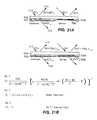
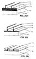
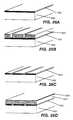
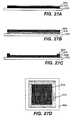
- FIGS. 20A through 20Dare perspective views of a cavity device.
- the effective length (Y) of bases 86 , 88 from arms 90 , 92 to circuit module 46is also a function of the dipole antenna's resonant wavelength; for a resonant wavelength of lambda, Y is a multiple of lambda.
- the arraycould be fabricated on a transparent substrate, thus facilitating transmissive operation.
- photoresist layer 716has been spun-on and patterned in a manner discussed above.
- the stencilis subsequently removed using an ultrasonic acetone bath and methanol rinse.
Landscapes
- Physics & Mathematics (AREA)
- General Physics & Mathematics (AREA)
- Engineering & Computer Science (AREA)
- Optics & Photonics (AREA)
- Theoretical Computer Science (AREA)
- Computer Hardware Design (AREA)
- Spectroscopy & Molecular Physics (AREA)
- Chemical & Material Sciences (AREA)
- Nonlinear Science (AREA)
- Crystallography & Structural Chemistry (AREA)
- Electromagnetism (AREA)
- Nanotechnology (AREA)
- Microelectronics & Electronic Packaging (AREA)
- Life Sciences & Earth Sciences (AREA)
- Biophysics (AREA)
- Mechanical Light Control Or Optical Switches (AREA)
Abstract
Description
- (1) U.S. patent application Ser. No. 08/769,947, filed Dec. 19, 1996 (now abandoned),
- (2) U.S. patent application Ser. No. 08/554,630, filed Nov. 6, 1995 (now abandoned), and
- (3) U.S. patent application Ser. No. 08/238,750, filed May 5, 1994 (now U.S. Pat. No. 5,835,255).
whereE (overbar) is the complex amplitude of the electric field of the sum of the transmitted wave and the reflected wave;E0is the complex amplitude of the electric field of the transmitted 20 wave;Er, is the complex amplitude of the electric field of the reflective wave; x(hat) is the orientation of the electric field of the wave;H is the amplitude of the magnetic field; y(hat) is the orientation of the magnetic field; μo is the permeability of free space; ∈ois the permittivity of free space; k=ωsqrt[μ0∈0] is the wavenumber; and η=sqrt [μ0/∈0] is the impedance of free space. For z>0 (i.e., within free space) only the transmitted wave exists and is represented by
E(overbar) is the complex amplitude the transmitted wave at z=0, kt=sqrt [μe] is its wavenumber; η=sqrt [μ/∈] is the impedance of the medium, i.e. z>0. Boundary conditions (z=0) for tangential electric fields are imposed on
{circumflex over (x)}[E0+Ex]={circumflex over (x)}Et (5)
In the same way, continuity for tangential magnetic fields (z=0) at the boundary yields,
ŷ(1/η0)(E0−ER)=ŷ(1/ηt)Et (6)
Dividing
1+Er/E0=Et/E0 (7)
1−ER/E0=(θ0/ηt)(Et/E0) (8)
Er/E0is called Γ and is the complex reflection coefficient while Et/η0=T is called the complex transmission coefficient, and ηt/η0=ηnis the normalized wave impedance. Solving for T and Γ yields
For matched impedance values, η0=ηn, the reflection coefficient is zero, and T=1 (i.e., no reflection), and in the case of a load at the boundary, a matched antenna, there is complete absorption.
I=jωg (11)
whereq is the charge density; z(hat) indicates the direction of the current (along the z-axis); ω is angular frequency; and d is the distance between ideal point charges representing the dipole. The vector potentialA(overbar) in polar coordinates is given by
where θ represents the angle relative to the dipole; θ(hat) is the angular orientation of the wave; μ0is the permeability of free space; r is radius from the dipole; r(hat) is radial orientation of the wave; Aris the radial component of the vector potential; Aθ is the angular component of the vector potential; and k is a factor which is used to represent sinusoidally varying waves. The H field is given by
where φ is elevation, with respect to the dipole. The E field is given by,
The far-field equation is given by
V(z)=V+e−jkz+ΓLejkz (17)
Because zL=z0, ΓL=0, and equation 17 simplifies to
V(z)=V+e−jkz (18)
Claims (53)
Priority Applications (2)
| Application Number | Priority Date | Filing Date | Title |
|---|---|---|---|
| US11/267,939US8014059B2 (en) | 1994-05-05 | 2005-11-04 | System and method for charge control in a MEMS device |
| US13/225,357US20120062310A1 (en) | 1994-05-05 | 2011-09-02 | System and method for charge control in a mems device |
Applications Claiming Priority (18)
| Application Number | Priority Date | Filing Date | Title |
|---|---|---|---|
| US08/238,750US5835255A (en) | 1986-04-23 | 1994-05-05 | Visible spectrum modulator arrays |
| PCT/US1995/005358WO1995030924A1 (en) | 1994-05-05 | 1995-05-01 | Visible spectrum modulator arrays |
| US55463095A | 1995-11-06 | 1995-11-06 | |
| US08/744,253US5986796A (en) | 1993-03-17 | 1996-11-05 | Visible spectrum modulator arrays |
| US76994796A | 1996-12-19 | 1996-12-19 | |
| US09/056,975US6674562B1 (en) | 1994-05-05 | 1998-04-08 | Interferometric modulation of radiation |
| US09/378,143US20010003487A1 (en) | 1996-11-05 | 1999-08-20 | Visible spectrum modulator arrays |
| US09/413,222US7123216B1 (en) | 1994-05-05 | 1999-10-05 | Photonic MEMS and structures |
| US09/875,401US7138984B1 (en) | 2001-06-05 | 2001-06-05 | Directly laminated touch sensitive screen |
| US09/966,843US6867896B2 (en) | 1994-05-05 | 2001-09-28 | Interferometric modulation of radiation |
| US09/991,378US20020075555A1 (en) | 1994-05-05 | 2001-11-21 | Interferometric modulation of radiation |
| US10/078,282US7042643B2 (en) | 1994-05-05 | 2002-02-19 | Interferometric modulation of radiation |
| US10/082,397US7126738B2 (en) | 1995-05-01 | 2002-02-25 | Visible spectrum modulator arrays |
| US10/251,196US7550794B2 (en) | 2002-09-20 | 2002-09-20 | Micromechanical systems device comprising a displaceable electrode and a charge-trapping layer |
| US10/414,594US7297471B1 (en) | 2003-04-15 | 2003-04-15 | Method for manufacturing an array of interferometric modulators |
| US10/644,312US7460291B2 (en) | 1994-05-05 | 2003-08-19 | Separable modulator |
| US11/056,571US7379227B2 (en) | 1994-05-05 | 2005-02-11 | Method and device for modulating light |
| US11/267,939US8014059B2 (en) | 1994-05-05 | 2005-11-04 | System and method for charge control in a MEMS device |
Related Parent Applications (7)
| Application Number | Title | Priority Date | Filing Date |
|---|---|---|---|
| US09/413,222Continuation-In-PartUS7123216B1 (en) | 1994-05-05 | 1999-10-05 | Photonic MEMS and structures |
| US09/875,401Continuation-In-PartUS7138984B1 (en) | 1994-05-05 | 2001-06-05 | Directly laminated touch sensitive screen |
| US10/082,397Continuation-In-PartUS7126738B2 (en) | 1994-05-05 | 2002-02-25 | Visible spectrum modulator arrays |
| US10/251,196Continuation-In-PartUS7550794B2 (en) | 1994-05-05 | 2002-09-20 | Micromechanical systems device comprising a displaceable electrode and a charge-trapping layer |
| US10/414,594Continuation-In-PartUS7297471B1 (en) | 1994-05-05 | 2003-04-15 | Method for manufacturing an array of interferometric modulators |
| US10/644,312Continuation-In-PartUS7460291B2 (en) | 1994-05-05 | 2003-08-19 | Separable modulator |
| US11/056,571Continuation-In-PartUS7379227B2 (en) | 1993-03-17 | 2005-02-11 | Method and device for modulating light |
Related Child Applications (4)
| Application Number | Title | Priority Date | Filing Date |
|---|---|---|---|
| US55463095AContinuation-In-Part | 1993-03-17 | 1995-11-06 | |
| US08/744,253ContinuationUS5986796A (en) | 1993-03-17 | 1996-11-05 | Visible spectrum modulator arrays |
| US09/991,378ContinuationUS20020075555A1 (en) | 1994-05-05 | 2001-11-21 | Interferometric modulation of radiation |
| US13/225,357DivisionUS20120062310A1 (en) | 1994-05-05 | 2011-09-02 | System and method for charge control in a mems device |
Publications (2)
| Publication Number | Publication Date |
|---|---|
| US20070058095A1 US20070058095A1 (en) | 2007-03-15 |
| US8014059B2true US8014059B2 (en) | 2011-09-06 |
Family
ID=46325114
Family Applications (2)
| Application Number | Title | Priority Date | Filing Date |
|---|---|---|---|
| US11/267,939Expired - Fee RelatedUS8014059B2 (en) | 1994-05-05 | 2005-11-04 | System and method for charge control in a MEMS device |
| US13/225,357AbandonedUS20120062310A1 (en) | 1994-05-05 | 2011-09-02 | System and method for charge control in a mems device |
Family Applications After (1)
| Application Number | Title | Priority Date | Filing Date |
|---|---|---|---|
| US13/225,357AbandonedUS20120062310A1 (en) | 1994-05-05 | 2011-09-02 | System and method for charge control in a mems device |
Country Status (1)
| Country | Link |
|---|---|
| US (2) | US8014059B2 (en) |
Cited By (7)
| Publication number | Priority date | Publication date | Assignee | Title |
|---|---|---|---|---|
| US8928967B2 (en) | 1998-04-08 | 2015-01-06 | Qualcomm Mems Technologies, Inc. | Method and device for modulating light |
| US8970939B2 (en) | 2004-09-27 | 2015-03-03 | Qualcomm Mems Technologies, Inc. | Method and device for multistate interferometric light modulation |
| US8971675B2 (en) | 2006-01-13 | 2015-03-03 | Qualcomm Mems Technologies, Inc. | Interconnect structure for MEMS device |
| US8988760B2 (en) | 2008-07-17 | 2015-03-24 | Qualcomm Mems Technologies, Inc. | Encapsulated electromechanical devices |
| US9001412B2 (en) | 2004-09-27 | 2015-04-07 | Qualcomm Mems Technologies, Inc. | Electromechanical device with optical function separated from mechanical and electrical function |
| US9110289B2 (en) | 1998-04-08 | 2015-08-18 | Qualcomm Mems Technologies, Inc. | Device for modulating light with multiple electrodes |
| US9554213B2 (en) | 2012-10-01 | 2017-01-24 | The Research Foundation For The State University Of New York | Hinged MEMS diaphragm |
Families Citing this family (12)
| Publication number | Priority date | Publication date | Assignee | Title |
|---|---|---|---|---|
| US6674562B1 (en)* | 1994-05-05 | 2004-01-06 | Iridigm Display Corporation | Interferometric modulation of radiation |
| US6829132B2 (en)* | 2003-04-30 | 2004-12-07 | Hewlett-Packard Development Company, L.P. | Charge control of micro-electromechanical device |
| US7889163B2 (en)* | 2004-08-27 | 2011-02-15 | Qualcomm Mems Technologies, Inc. | Drive method for MEMS devices |
| US7630121B2 (en) | 2007-07-02 | 2009-12-08 | Qualcomm Mems Technologies, Inc. | Electromechanical device with optical function separated from mechanical and electrical function |
| KR101415566B1 (en)* | 2007-10-29 | 2014-07-04 | 삼성디스플레이 주식회사 | Display device |
| US7944604B2 (en) | 2008-03-07 | 2011-05-17 | Qualcomm Mems Technologies, Inc. | Interferometric modulator in transmission mode |
| US8660500B2 (en)* | 2009-06-09 | 2014-02-25 | Broadcom Corporation | Method and system for a voltage-controlled oscillator with a leaky wave antenna |
| US7990604B2 (en) | 2009-06-15 | 2011-08-02 | Qualcomm Mems Technologies, Inc. | Analog interferometric modulator |
| US8760751B2 (en) | 2012-01-26 | 2014-06-24 | Qualcomm Mems Technologies, Inc. | Analog IMOD having a color notch filter |
| US20140125707A1 (en)* | 2012-11-06 | 2014-05-08 | Qualcomm Mems Technologies, Inc. | Color performance and image quality using field sequential color (fsc) together with single-mirror imods |
| DE102015206774B4 (en)* | 2015-04-15 | 2018-10-25 | Fraunhofer-Gesellschaft zur Förderung der angewandten Forschung e.V. | Micromechanical device with an actively bendable element |
| CN115294933B (en)* | 2022-09-26 | 2023-01-10 | 惠科股份有限公司 | Display panel, display module and display device |
Citations (283)
| Publication number | Priority date | Publication date | Assignee | Title |
|---|---|---|---|---|
| US2534846A (en) | 1946-06-20 | 1950-12-19 | Emi Ltd | Color filter |
| US3439973A (en) | 1963-06-28 | 1969-04-22 | Siemens Ag | Polarizing reflector for electromagnetic wave radiation in the micron wavelength |
| US3653741A (en) | 1970-02-16 | 1972-04-04 | Alvin M Marks | Electro-optical dipolar material |
| US3656836A (en) | 1968-07-05 | 1972-04-18 | Thomson Csf | Light modulator |
| US3679313A (en) | 1970-10-23 | 1972-07-25 | Bell Telephone Labor Inc | Dispersive element for optical pulse compression |
| US3701586A (en) | 1971-04-21 | 1972-10-31 | George G Goetz | Light modulating deflectable membrane |
| US3725868A (en) | 1970-10-19 | 1973-04-03 | Burroughs Corp | Small reconfigurable processor for a variety of data processing applications |
| US3728030A (en) | 1970-06-22 | 1973-04-17 | Cary Instruments | Polarization interferometer |
| US3813265A (en) | 1970-02-16 | 1974-05-28 | A Marks | Electro-optical dipolar material |
| US3955190A (en) | 1972-09-11 | 1976-05-04 | Kabushiki Kaisha Suwa Seikosha | Electro-optical digital display |
| US3955880A (en) | 1973-07-20 | 1976-05-11 | Organisation Europeenne De Recherches Spatiales | Infrared radiation modulator |
| US4099854A (en) | 1976-10-12 | 1978-07-11 | The Unites States Of America As Represented By The Secretary Of The Navy | Optical notch filter utilizing electric dipole resonance absorption |
| US4190488A (en) | 1978-08-21 | 1980-02-26 | International Business Machines Corporation | Etching method using noble gas halides |
| US4228437A (en) | 1979-06-26 | 1980-10-14 | The United States Of America As Represented By The Secretary Of The Navy | Wideband polarization-transforming electromagnetic mirror |
| US4377324A (en) | 1980-08-04 | 1983-03-22 | Honeywell Inc. | Graded index Fabry-Perot optical filter device |
| US4389096A (en) | 1977-12-27 | 1983-06-21 | Matsushita Electric Industrial Co., Ltd. | Image display apparatus of liquid crystal valve projection type |
| US4392711A (en) | 1980-03-28 | 1983-07-12 | Hoechst Aktiengesellschaft | Process and apparatus for rendering visible charge images |
| US4403248A (en) | 1980-03-04 | 1983-09-06 | U.S. Philips Corporation | Display device with deformable reflective medium |
| US4408181A (en) | 1979-04-10 | 1983-10-04 | Tokyo Shibaura Denki Kabushiki Kaisha | Document data filing/retrieval system |
| US4425572A (en) | 1980-05-16 | 1984-01-10 | Sharp Kabushiki Kaisha | Thin film transistor |
| US4441791A (en) | 1980-09-02 | 1984-04-10 | Texas Instruments Incorporated | Deformable mirror light modulator |
| US4445050A (en) | 1981-12-15 | 1984-04-24 | Marks Alvin M | Device for conversion of light power to electric power |
| US4482213A (en) | 1982-11-23 | 1984-11-13 | Texas Instruments Incorporated | Perimeter seal reinforcement holes for plastic LCDs |
| US4498953A (en) | 1983-07-27 | 1985-02-12 | At&T Bell Laboratories | Etching techniques |
| US4500171A (en) | 1982-06-02 | 1985-02-19 | Texas Instruments Incorporated | Process for plastic LCD fill hole sealing |
| US4519676A (en) | 1982-02-01 | 1985-05-28 | U.S. Philips Corporation | Passive display device |
| US4531126A (en) | 1981-05-18 | 1985-07-23 | Societe D'etude Du Radant | Method and device for analyzing a very high frequency radiation beam of electromagnetic waves |
| US4560435A (en) | 1984-10-01 | 1985-12-24 | International Business Machines Corporation | Composite back-etch/lift-off stencil for proximity effect minimization |
| US4566935A (en) | 1984-07-31 | 1986-01-28 | Texas Instruments Incorporated | Spatial light modulator and method |
| US4571603A (en) | 1981-11-03 | 1986-02-18 | Texas Instruments Incorporated | Deformable mirror electrostatic printer |
| US4596992A (en) | 1984-08-31 | 1986-06-24 | Texas Instruments Incorporated | Linear spatial light modulator and printer |
| US4615595A (en) | 1984-10-10 | 1986-10-07 | Texas Instruments Incorporated | Frame addressed spatial light modulator |
| US4655554A (en) | 1985-03-06 | 1987-04-07 | The United States Of America As Represented By The Secretary Of The Air Force | Spatial light modulator having a capacitively coupled photoconductor |
| US4663083A (en) | 1978-05-26 | 1987-05-05 | Marks Alvin M | Electro-optical dipole suspension with reflective-absorptive-transmissive characteristics |
| US4662746A (en) | 1985-10-30 | 1987-05-05 | Texas Instruments Incorporated | Spatial light modulator and method |
| US4672254A (en) | 1985-10-11 | 1987-06-09 | Massachusetts Institute Of Technology | Surface acoustic wave devices and method of manufacture thereof |
| US4681403A (en) | 1981-07-16 | 1987-07-21 | U.S. Philips Corporation | Display device with micromechanical leaf spring switches |
| US4710732A (en) | 1984-07-31 | 1987-12-01 | Texas Instruments Incorporated | Spatial light modulator and method |
| US4748366A (en) | 1986-09-02 | 1988-05-31 | Taylor George W | Novel uses of piezoelectric materials for creating optical effects |
| US4786128A (en) | 1986-12-02 | 1988-11-22 | Quantum Diagnostics, Ltd. | Device for modulating and reflecting electromagnetic radiation employing electro-optic layer having a variable index of refraction |
| US4790635A (en) | 1986-04-25 | 1988-12-13 | The Secretary Of State For Defence In Her Brittanic Majesty's Government Of The United Kingdom Of Great Britain And Northern Ireland | Electro-optical device |
| US4857978A (en) | 1987-08-11 | 1989-08-15 | North American Philips Corporation | Solid state light modulator incorporating metallized gel and method of metallization |
| US4856863A (en) | 1988-06-22 | 1989-08-15 | Texas Instruments Incorporated | Optical fiber interconnection network including spatial light modulator |
| US4859060A (en) | 1985-11-26 | 1989-08-22 | 501 Sharp Kabushiki Kaisha | Variable interferometric device and a process for the production of the same |
| US4880493A (en) | 1988-06-16 | 1989-11-14 | The United States Of America As Represented By The United States Department Of Energy | Electronic-carrier-controlled photochemical etching process in semiconductor device fabrication |
| US4896033A (en) | 1986-04-22 | 1990-01-23 | Thomson-Csf | Array of optically-controlled elements for the diffusion of electromagnetic energy |
| US4900136A (en) | 1987-08-11 | 1990-02-13 | North American Philips Corporation | Method of metallizing silica-containing gel and solid state light modulator incorporating the metallized gel |
| US4900395A (en) | 1989-04-07 | 1990-02-13 | Fsi International, Inc. | HF gas etching of wafers in an acid processor |
| US4925259A (en) | 1988-10-20 | 1990-05-15 | The United States Of America As Represented By The United States Department Of Energy | Multilayer optical dielectric coating |
| US4952034A (en) | 1985-05-10 | 1990-08-28 | Hitachi, Ltd. | Liquid crystal projection display |
| US4954789A (en) | 1989-09-28 | 1990-09-04 | Texas Instruments Incorporated | Spatial light modulator |
| US4956213A (en) | 1988-02-17 | 1990-09-11 | Fuji Photo Film Co., Ltd. | Information recording medium |
| US4956619A (en) | 1988-02-19 | 1990-09-11 | Texas Instruments Incorporated | Spatial light modulator |
| US4963245A (en) | 1986-05-02 | 1990-10-16 | Ciba Corning Diagnostics Corp. | Unitary multiple electrode sensor |
| US4965562A (en) | 1987-05-13 | 1990-10-23 | U.S. Philips Corporation | Electroscopic display device |
| US4982184A (en) | 1989-01-03 | 1991-01-01 | General Electric Company | Electrocrystallochromic display and element |
| US5018256A (en) | 1990-06-29 | 1991-05-28 | Texas Instruments Incorporated | Architecture and process for integrating DMD with control circuit substrates |
| US5022745A (en) | 1989-09-07 | 1991-06-11 | Massachusetts Institute Of Technology | Electrostatically deformable single crystal dielectrically coated mirror |
| US5028939A (en) | 1988-08-23 | 1991-07-02 | Texas Instruments Incorporated | Spatial light modulator system |
| US5034351A (en) | 1990-10-01 | 1991-07-23 | Motorola, Inc. | Process for forming a feature on a substrate without recessing the surface of the substrate |
| US5037173A (en) | 1989-11-22 | 1991-08-06 | Texas Instruments Incorporated | Optical interconnection network |
| US5044736A (en) | 1990-11-06 | 1991-09-03 | Motorola, Inc. | Configurable optical filter or display |
| US5061049A (en) | 1984-08-31 | 1991-10-29 | Texas Instruments Incorporated | Spatial light modulator and method |
| US5075796A (en) | 1990-05-31 | 1991-12-24 | Eastman Kodak Company | Optical article for multicolor imaging |
| US5079544A (en) | 1989-02-27 | 1992-01-07 | Texas Instruments Incorporated | Standard independent digitized video system |
| US5078479A (en) | 1990-04-20 | 1992-01-07 | Centre Suisse D'electronique Et De Microtechnique Sa | Light modulation device with matrix addressing |
| US5083857A (en) | 1990-06-29 | 1992-01-28 | Texas Instruments Incorporated | Multi-level deformable mirror device |
| US5096279A (en) | 1984-08-31 | 1992-03-17 | Texas Instruments Incorporated | Spatial light modulator and method |
| US5099353A (en) | 1990-06-29 | 1992-03-24 | Texas Instruments Incorporated | Architecture and process for integrating DMD with control circuit substrates |
| US5114226A (en) | 1987-03-20 | 1992-05-19 | Digital Optronics Corporation | 3-Dimensional vision system utilizing coherent optical detection |
| US5124834A (en) | 1989-11-16 | 1992-06-23 | General Electric Company | Transferrable, self-supporting pellicle for elastomer light valve displays and method for making the same |
| US5136669A (en) | 1991-03-15 | 1992-08-04 | Sperry Marine Inc. | Variable ratio fiber optic coupler optical signal processing element |
| US5142405A (en) | 1990-06-29 | 1992-08-25 | Texas Instruments Incorporated | Bistable dmd addressing circuit and method |
| US5142414A (en)* | 1991-04-22 | 1992-08-25 | Koehler Dale R | Electrically actuatable temporal tristimulus-color device |
| US5153771A (en) | 1990-07-18 | 1992-10-06 | Northrop Corporation | Coherent light modulation and detector |
| US5162787A (en) | 1989-02-27 | 1992-11-10 | Texas Instruments Incorporated | Apparatus and method for digitized video system utilizing a moving display surface |
| US5168406A (en) | 1991-07-31 | 1992-12-01 | Texas Instruments Incorporated | Color deformable mirror device and method for manufacture |
| US5170156A (en) | 1989-02-27 | 1992-12-08 | Texas Instruments Incorporated | Multi-frequency two dimensional display system |
| US5170283A (en) | 1991-07-24 | 1992-12-08 | Northrop Corporation | Silicon spatial light modulator |
| US5172262A (en) | 1985-10-30 | 1992-12-15 | Texas Instruments Incorporated | Spatial light modulator and method |
| US5179274A (en) | 1991-07-12 | 1993-01-12 | Texas Instruments Incorporated | Method for controlling operation of optical systems and devices |
| US5192946A (en) | 1989-02-27 | 1993-03-09 | Texas Instruments Incorporated | Digitized color video display system |
| US5192395A (en) | 1990-10-12 | 1993-03-09 | Texas Instruments Incorporated | Method of making a digital flexure beam accelerometer |
| US5198644A (en) | 1989-05-05 | 1993-03-30 | Diablo Research Corporation | System for display of prices and related method |
| US5206632A (en) | 1989-09-11 | 1993-04-27 | Deutsche Thomson-Brandt Gmbh | Actuating circuit for a liquid crystal display |
| US5206629A (en) | 1989-02-27 | 1993-04-27 | Texas Instruments Incorporated | Spatial light modulator and memory for digitized video display |
| US5212582A (en) | 1992-03-04 | 1993-05-18 | Texas Instruments Incorporated | Electrostatically controlled beam steering device and method |
| US5214419A (en) | 1989-02-27 | 1993-05-25 | Texas Instruments Incorporated | Planarized true three dimensional display |
| US5214420A (en) | 1989-02-27 | 1993-05-25 | Texas Instruments Incorporated | Spatial light modulator projection system with random polarity light |
| US5216537A (en) | 1990-06-29 | 1993-06-01 | Texas Instruments Incorporated | Architecture and process for integrating DMD with control circuit substrates |
| US5226099A (en) | 1991-04-26 | 1993-07-06 | Texas Instruments Incorporated | Digital micromirror shutter device |
| US5228013A (en) | 1992-01-10 | 1993-07-13 | Bik Russell J | Clock-painting device and method for indicating the time-of-day with a non-traditional, now analog artistic panel of digital electronic visual displays |
| US5231532A (en) | 1992-02-05 | 1993-07-27 | Texas Instruments Incorporated | Switchable resonant filter for optical radiation |
| US5233459A (en) | 1991-03-06 | 1993-08-03 | Massachusetts Institute Of Technology | Electric display device |
| US5233456A (en) | 1991-12-20 | 1993-08-03 | Texas Instruments Incorporated | Resonant mirror and method of manufacture |
| US5233385A (en) | 1991-12-18 | 1993-08-03 | Texas Instruments Incorporated | White light enhanced color field sequential projection |
| US5254980A (en) | 1991-09-06 | 1993-10-19 | Texas Instruments Incorporated | DMD display system controller |
| JPH05275401A (en)* | 1992-03-24 | 1993-10-22 | Yokogawa Electric Corp | Etching method for sacrifice layer |
| US5262667A (en) | 1990-09-07 | 1993-11-16 | Sony Corporation | Semiconductor device for optical pick-up |
| US5272473A (en) | 1989-02-27 | 1993-12-21 | Texas Instruments Incorporated | Reduced-speckle display system |
| US5278652A (en) | 1991-04-01 | 1994-01-11 | Texas Instruments Incorporated | DMD architecture and timing for use in a pulse width modulated display system |
| US5280277A (en) | 1990-06-29 | 1994-01-18 | Texas Instruments Incorporated | Field updated deformable mirror device |
| US5285196A (en) | 1992-10-15 | 1994-02-08 | Texas Instruments Incorporated | Bistable DMD addressing method |
| US5287096A (en) | 1989-02-27 | 1994-02-15 | Texas Instruments Incorporated | Variable luminosity display system |
| US5293272A (en) | 1992-08-24 | 1994-03-08 | Physical Optics Corporation | High finesse holographic fabry-perot etalon and method of fabricating |
| US5296950A (en) | 1992-01-31 | 1994-03-22 | Texas Instruments Incorporated | Optical signal free-space conversion board |
| US5311360A (en) | 1992-04-28 | 1994-05-10 | The Board Of Trustees Of The Leland Stanford, Junior University | Method and apparatus for modulating a light beam |
| US5312513A (en) | 1992-04-03 | 1994-05-17 | Texas Instruments Incorporated | Methods of forming multiple phase light modulators |
| US5315370A (en) | 1991-10-23 | 1994-05-24 | Bulow Jeffrey A | Interferometric modulator for optical signal processing |
| US5323002A (en) | 1992-03-25 | 1994-06-21 | Texas Instruments Incorporated | Spatial light modulator based optical calibration system |
| US5324683A (en) | 1993-06-02 | 1994-06-28 | Motorola, Inc. | Method of forming a semiconductor structure having an air region |
| US5325116A (en) | 1992-09-18 | 1994-06-28 | Texas Instruments Incorporated | Device for writing to and reading from optical storage media |
| US5326430A (en) | 1992-09-24 | 1994-07-05 | International Business Machines Corporation | Cooling microfan arrangements and process |
| US5327286A (en) | 1992-08-31 | 1994-07-05 | Texas Instruments Incorporated | Real time optical correlation system |
| US5331454A (en) | 1990-11-13 | 1994-07-19 | Texas Instruments Incorporated | Low reset voltage process for DMD |
| US5337191A (en) | 1993-04-13 | 1994-08-09 | Photran Corporation | Broad band pass filter including metal layers and dielectric layers of alternating refractive index |
| US5355357A (en) | 1990-01-20 | 1994-10-11 | Sony Corporation | Disc player and disc loading device |
| US5355181A (en) | 1990-08-20 | 1994-10-11 | Sony Corporation | Apparatus for direct display of an image on the retina of the eye using a scanning laser |
| US5358601A (en) | 1991-09-24 | 1994-10-25 | Micron Technology, Inc. | Process for isotropically etching semiconductor devices |
| US5361383A (en) | 1991-10-30 | 1994-11-01 | Hughes Aircraft Company | Optical fiber having internal partial mirrors and interferometer using same |
| US5365283A (en) | 1993-07-19 | 1994-11-15 | Texas Instruments Incorporated | Color phase control for projection display using spatial light modulator |
| US5381253A (en) | 1991-11-14 | 1995-01-10 | Board Of Regents Of University Of Colorado | Chiral smectic liquid crystal optical modulators having variable retardation |
| US5401983A (en) | 1992-04-08 | 1995-03-28 | Georgia Tech Research Corporation | Processes for lift-off of thin film materials or devices for fabricating three dimensional integrated circuits, optical detectors, and micromechanical devices |
| US5422310A (en) | 1993-02-09 | 1995-06-06 | Sony Corporation | Method of forming interconnection in semiconductor device |
| EP0667548A1 (en)* | 1994-01-27 | 1995-08-16 | AT&T Corp. | Micromechanical modulator |
| US5444566A (en) | 1994-03-07 | 1995-08-22 | Texas Instruments Incorporated | Optimized electronic operation of digital micromirror devices |
| US5446479A (en) | 1989-02-27 | 1995-08-29 | Texas Instruments Incorporated | Multi-dimensional array video processor system |
| US5448314A (en) | 1994-01-07 | 1995-09-05 | Texas Instruments | Method and apparatus for sequential color imaging |
| US5452138A (en) | 1991-07-31 | 1995-09-19 | Texas Instruments Incorporated | Deformable mirror device with integral color filter |
| US5452024A (en) | 1993-11-01 | 1995-09-19 | Texas Instruments Incorporated | DMD display system |
| US5454904A (en) | 1993-01-04 | 1995-10-03 | General Electric Company | Micromachining methods for making micromechanical moving structures including multiple contact switching system |
| US5454906A (en) | 1994-06-21 | 1995-10-03 | Texas Instruments Inc. | Method of providing sacrificial spacer for micro-mechanical devices |
| US5457493A (en) | 1993-09-15 | 1995-10-10 | Texas Instruments Incorporated | Digital micro-mirror based image simulation system |
| US5457566A (en) | 1991-11-22 | 1995-10-10 | Texas Instruments Incorporated | DMD scanner |
| US5459602A (en) | 1993-10-29 | 1995-10-17 | Texas Instruments | Micro-mechanical optical shutter |
| US5457900A (en) | 1994-03-31 | 1995-10-17 | Roy; Avery J. | Footwear display device |
| US5461411A (en) | 1993-03-29 | 1995-10-24 | Texas Instruments Incorporated | Process and architecture for digital micromirror printer |
| WO1995030924A1 (en)* | 1994-05-05 | 1995-11-16 | Etalon, Inc. | Visible spectrum modulator arrays |
| US5474865A (en) | 1994-11-21 | 1995-12-12 | Sematech, Inc. | Globally planarized binary optical mask using buried absorbers |
| US5489952A (en) | 1993-07-14 | 1996-02-06 | Texas Instruments Incorporated | Method and device for multi-format television |
| US5497172A (en) | 1994-06-13 | 1996-03-05 | Texas Instruments Incorporated | Pulse width modulation for spatial light modulator with split reset addressing |
| US5497197A (en) | 1993-11-04 | 1996-03-05 | Texas Instruments Incorporated | System and method for packaging data into video processor |
| US5499062A (en) | 1994-06-23 | 1996-03-12 | Texas Instruments Incorporated | Multiplexed memory timing with block reset and secondary memory |
| US5499037A (en) | 1988-09-30 | 1996-03-12 | Sharp Kabushiki Kaisha | Liquid crystal display device for display with gray levels |
| US5500635A (en) | 1990-02-20 | 1996-03-19 | Mott; Jonathan C. | Products incorporating piezoelectric material |
| US5506597A (en) | 1989-02-27 | 1996-04-09 | Texas Instruments Incorporated | Apparatus and method for image projection |
| US5517347A (en) | 1993-12-01 | 1996-05-14 | Texas Instruments Incorporated | Direct view deformable mirror device |
| US5526172A (en) | 1993-07-27 | 1996-06-11 | Texas Instruments Incorporated | Microminiature, monolithic, variable electrical signal processor and apparatus including same |
| US5526051A (en) | 1993-10-27 | 1996-06-11 | Texas Instruments Incorporated | Digital television system |
| US5526327A (en) | 1994-03-15 | 1996-06-11 | Cordova, Jr.; David J. | Spatial displacement time display |
| US5526688A (en) | 1990-10-12 | 1996-06-18 | Texas Instruments Incorporated | Digital flexure beam accelerometer and method |
| US5535047A (en) | 1995-04-18 | 1996-07-09 | Texas Instruments Incorporated | Active yoke hidden hinge digital micromirror device |
| US5548301A (en) | 1993-01-11 | 1996-08-20 | Texas Instruments Incorporated | Pixel control circuitry for spatial light modulator |
| US5552925A (en) | 1993-09-07 | 1996-09-03 | John M. Baker | Electro-micro-mechanical shutters on transparent substrates |
| US5552924A (en) | 1994-11-14 | 1996-09-03 | Texas Instruments Incorporated | Micromechanical device having an improved beam |
| US5559358A (en) | 1993-05-25 | 1996-09-24 | Honeywell Inc. | Opto-electro-mechanical device or filter, process for making, and sensors made therefrom |
| US5563398A (en) | 1991-10-31 | 1996-10-08 | Texas Instruments Incorporated | Spatial light modulator scanning system |
| US5567334A (en) | 1995-02-27 | 1996-10-22 | Texas Instruments Incorporated | Method for creating a digital micromirror device using an aluminum hard mask |
| US5579149A (en) | 1993-09-13 | 1996-11-26 | Csem Centre Suisse D'electronique Et De Microtechnique Sa | Miniature network of light obturators |
| US5581272A (en) | 1993-08-25 | 1996-12-03 | Texas Instruments Incorporated | Signal generator for controlling a spatial light modulator |
| US5583688A (en) | 1993-12-21 | 1996-12-10 | Texas Instruments Incorporated | Multi-level digital micromirror device |
| US5597736A (en) | 1992-08-11 | 1997-01-28 | Texas Instruments Incorporated | High-yield spatial light modulator with light blocking layer |
| US5602671A (en) | 1990-11-13 | 1997-02-11 | Texas Instruments Incorporated | Low surface energy passivation layer for micromechanical devices |
| US5610625A (en) | 1992-05-20 | 1997-03-11 | Texas Instruments Incorporated | Monolithic spatial light modulator and memory package |
| US5610438A (en) | 1995-03-08 | 1997-03-11 | Texas Instruments Incorporated | Micro-mechanical device with non-evaporable getter |
| US5610624A (en) | 1994-11-30 | 1997-03-11 | Texas Instruments Incorporated | Spatial light modulator with reduced possibility of an on state defect |
| US5619059A (en) | 1994-09-28 | 1997-04-08 | National Research Council Of Canada | Color deformable mirror device having optical thin film interference color coatings |
| US5619366A (en) | 1992-06-08 | 1997-04-08 | Texas Instruments Incorporated | Controllable surface filter |
| US5629790A (en) | 1993-10-18 | 1997-05-13 | Neukermans; Armand P. | Micromachined torsional scanner |
| WO1997017628A1 (en)* | 1995-11-06 | 1997-05-15 | Etalon, Inc. | Interferometric modulation |
| US5633652A (en) | 1984-02-17 | 1997-05-27 | Canon Kabushiki Kaisha | Method for driving optical modulation device |
| US5636052A (en) | 1994-07-29 | 1997-06-03 | Lucent Technologies Inc. | Direct view display based on a micromechanical modulation |
| US5636185A (en) | 1995-03-10 | 1997-06-03 | Boit Incorporated | Dynamically changing liquid crystal display timekeeping apparatus |
| US5638084A (en) | 1992-05-22 | 1997-06-10 | Dielectric Systems International, Inc. | Lighting-independent color video display |
| US5646768A (en) | 1994-07-29 | 1997-07-08 | Texas Instruments Incorporated | Support posts for micro-mechanical devices |
| US5650881A (en) | 1994-11-02 | 1997-07-22 | Texas Instruments Incorporated | Support post architecture for micromechanical devices |
| US5654741A (en) | 1994-05-17 | 1997-08-05 | Texas Instruments Incorporation | Spatial light modulator display pointing device |
| US5659374A (en) | 1992-10-23 | 1997-08-19 | Texas Instruments Incorporated | Method of repairing defective pixels |
| US5665997A (en) | 1994-03-31 | 1997-09-09 | Texas Instruments Incorporated | Grated landing area to eliminate sticking of micro-mechanical devices |
| US5673139A (en) | 1993-07-19 | 1997-09-30 | Medcom, Inc. | Microelectromechanical television scanning device and method for making the same |
| US5683591A (en) | 1993-05-25 | 1997-11-04 | Robert Bosch Gmbh | Process for producing surface micromechanical structures |
| US5703710A (en) | 1994-09-09 | 1997-12-30 | Deacon Research | Method for manipulating optical energy using poled structure |
| US5710656A (en) | 1996-07-30 | 1998-01-20 | Lucent Technologies Inc. | Micromechanical optical modulator having a reduced-mass composite membrane |
| US5726480A (en) | 1995-01-27 | 1998-03-10 | The Regents Of The University Of California | Etchants for use in micromachining of CMOS Microaccelerometers and microelectromechanical devices and method of making the same |
| US5739945A (en) | 1995-09-29 | 1998-04-14 | Tayebati; Parviz | Electrically tunable optical filter utilizing a deformable multi-layer mirror |
| US5745281A (en) | 1995-12-29 | 1998-04-28 | Hewlett-Packard Company | Electrostatically-driven light modulator and display |
| US5771116A (en) | 1996-10-21 | 1998-06-23 | Texas Instruments Incorporated | Multiple bias level reset waveform for enhanced DMD control |
| US5784190A (en) | 1995-04-27 | 1998-07-21 | John M. Baker | Electro-micro-mechanical shutters on transparent substrates |
| US5793504A (en) | 1996-08-07 | 1998-08-11 | Northrop Grumman Corporation | Hybrid angular/spatial holographic multiplexer |
| US5808780A (en) | 1997-06-09 | 1998-09-15 | Texas Instruments Incorporated | Non-contacting micromechanical optical switch |
| US5825528A (en) | 1995-12-26 | 1998-10-20 | Lucent Technologies Inc. | Phase-mismatched fabry-perot cavity micromechanical modulator |
| US5842088A (en) | 1994-06-17 | 1998-11-24 | Texas Instruments Incorporated | Method of calibrating a spatial light modulator printing system |
| US5912758A (en) | 1996-09-11 | 1999-06-15 | Texas Instruments Incorporated | Bipolar reset for spatial light modulators |
| US5943158A (en) | 1998-05-05 | 1999-08-24 | Lucent Technologies Inc. | Micro-mechanical, anti-reflection, switched optical modulator array and fabrication method |
| WO1999052006A2 (en)* | 1998-04-08 | 1999-10-14 | Etalon, Inc. | Interferometric modulation of radiation |
| US6028690A (en) | 1997-11-26 | 2000-02-22 | Texas Instruments Incorporated | Reduced micromirror mirror gaps for improved contrast ratio |
| US6031653A (en)* | 1997-08-28 | 2000-02-29 | California Institute Of Technology | Low-cost thin-metal-film interference filters |
| US6038056A (en) | 1997-05-08 | 2000-03-14 | Texas Instruments Incorporated | Spatial light modulator having improved contrast ratio |
| US6040937A (en) | 1994-05-05 | 2000-03-21 | Etalon, Inc. | Interferometric modulation |
| US6061075A (en) | 1992-01-23 | 2000-05-09 | Texas Instruments Incorporated | Non-systolic time delay and integration printing |
| US6099132A (en) | 1994-09-23 | 2000-08-08 | Texas Instruments Incorporated | Manufacture method for micromechanical devices |
| US6100872A (en) | 1993-05-25 | 2000-08-08 | Canon Kabushiki Kaisha | Display control method and apparatus |
| US6113239A (en) | 1998-09-04 | 2000-09-05 | Sharp Laboratories Of America, Inc. | Projection display system for reflective light valves |
| US6147790A (en) | 1998-06-02 | 2000-11-14 | Texas Instruments Incorporated | Spring-ring micromechanical device |
| US6160833A (en) | 1998-05-06 | 2000-12-12 | Xerox Corporation | Blue vertical cavity surface emitting laser |
| US6158156A (en) | 1995-10-30 | 2000-12-12 | John Mcgavigan Limited | Display panels |
| US6180428B1 (en) | 1997-12-12 | 2001-01-30 | Xerox Corporation | Monolithic scanning light emitting devices using micromachining |
| US6201633B1 (en) | 1999-06-07 | 2001-03-13 | Xerox Corporation | Micro-electromechanical based bistable color display sheets |
| US6232936B1 (en) | 1993-12-03 | 2001-05-15 | Texas Instruments Incorporated | DMD Architecture to improve horizontal resolution |
| US6243149B1 (en) | 1994-10-27 | 2001-06-05 | Massachusetts Institute Of Technology | Method of imaging using a liquid crystal display device |
| US20010003487A1 (en) | 1996-11-05 | 2001-06-14 | Mark W. Miles | Visible spectrum modulator arrays |
| US6282010B1 (en) | 1998-05-14 | 2001-08-28 | Texas Instruments Incorporated | Anti-reflective coatings for spatial light modulators |
| US6295154B1 (en) | 1998-06-05 | 2001-09-25 | Texas Instruments Incorporated | Optical switching apparatus |
| US6323982B1 (en) | 1998-05-22 | 2001-11-27 | Texas Instruments Incorporated | Yield superstructure for digital micromirror device |
| US6335831B2 (en) | 1998-12-18 | 2002-01-01 | Eastman Kodak Company | Multilevel mechanical grating device |
| US20020015215A1 (en) | 1994-05-05 | 2002-02-07 | Iridigm Display Corporation, A Delaware Corporation | Interferometric modulation of radiation |
| US20020021485A1 (en) | 2000-07-13 | 2002-02-21 | Nissim Pilossof | Blazed micro-mechanical light modulator and array thereof |
| US20020024711A1 (en) | 1994-05-05 | 2002-02-28 | Iridigm Display Corporation, A Delaware Corporation | Interferometric modulation of radiation |
| US20020051281A1 (en) | 2000-11-02 | 2002-05-02 | Fujitsu Limited | Galvano-mirror and method of making the same |
| US6384953B1 (en) | 2000-06-29 | 2002-05-07 | The United States Of America As Represented By The Secretary Of The Navy | Micro-dynamic optical device |
| US20020054424A1 (en) | 1994-05-05 | 2002-05-09 | Etalon, Inc. | Photonic mems and structures |
| US6407851B1 (en) | 2000-08-01 | 2002-06-18 | Mohammed N. Islam | Micromechanical optical switch |
| US6466358B2 (en) | 1999-12-30 | 2002-10-15 | Texas Instruments Incorporated | Analog pulse width modulation cell for digital micromechanical device |
| US6465355B1 (en) | 2001-04-27 | 2002-10-15 | Hewlett-Packard Company | Method of fabricating suspended microstructures |
| US20020149828A1 (en) | 1994-05-05 | 2002-10-17 | Miles Mark W. | Controlling micro-electro-mechanical cavities |
| US6473274B1 (en) | 2000-06-28 | 2002-10-29 | Texas Instruments Incorporated | Symmetrical microactuator structure for use in mass data storage devices, or the like |
| US6480177B2 (en) | 1997-06-04 | 2002-11-12 | Texas Instruments Incorporated | Blocked stepped address voltage for micromechanical devices |
| US6496122B2 (en) | 1998-06-26 | 2002-12-17 | Sharp Laboratories Of America, Inc. | Image display and remote control system capable of displaying two distinct images |
| WO2003007049A1 (en)* | 1999-10-05 | 2003-01-23 | Iridigm Display Corporation | Photonic mems and structures |
| US6545335B1 (en) | 1999-12-27 | 2003-04-08 | Xerox Corporation | Structure and method for electrical isolation of optoelectronic integrated circuits |
| US6548908B2 (en) | 1999-12-27 | 2003-04-15 | Xerox Corporation | Structure and method for planar lateral oxidation in passive devices |
| US6549338B1 (en) | 1999-11-12 | 2003-04-15 | Texas Instruments Incorporated | Bandpass filter to reduce thermal impact of dichroic light shift |
| US6552840B2 (en) | 1999-12-03 | 2003-04-22 | Texas Instruments Incorporated | Electrostatic efficiency of micromechanical devices |
| US6574033B1 (en) | 2002-02-27 | 2003-06-03 | Iridigm Display Corporation | Microelectromechanical systems device and method for fabricating same |
| US6589625B1 (en) | 2001-08-01 | 2003-07-08 | Iridigm Display Corporation | Hermetic seal and method to create the same |
| US6600201B2 (en) | 2001-08-03 | 2003-07-29 | Hewlett-Packard Development Company, L.P. | Systems with high density packing of micromachines |
| US6606175B1 (en) | 1999-03-16 | 2003-08-12 | Sharp Laboratories Of America, Inc. | Multi-segment light-emitting diode |
| WO2003069413A1 (en)* | 2002-02-12 | 2003-08-21 | Iridigm Display Corporation | A method for fabricating a structure for a microelectromechanical systems (mems) device |
| US6625047B2 (en) | 2000-12-31 | 2003-09-23 | Texas Instruments Incorporated | Micromechanical memory element |
| US6630786B2 (en) | 2001-03-30 | 2003-10-07 | Candescent Technologies Corporation | Light-emitting device having light-reflective layer formed with, or/and adjacent to, material that enhances device performance |
| US6632698B2 (en) | 2001-08-07 | 2003-10-14 | Hewlett-Packard Development Company, L.P. | Microelectromechanical device having a stiffened support beam, and methods of forming stiffened support beams in MEMS |
| US20030202266A1 (en) | 2002-04-30 | 2003-10-30 | Ring James W. | Micro-mirror device with light angle amplification |
| US20030202264A1 (en) | 2002-04-30 | 2003-10-30 | Weber Timothy L. | Micro-mirror device |
| US20030202265A1 (en) | 2002-04-30 | 2003-10-30 | Reboa Paul F. | Micro-mirror device including dielectrophoretic liquid |
| US6643069B2 (en) | 2000-08-31 | 2003-11-04 | Texas Instruments Incorporated | SLM-base color projection display having multiple SLM's and multiple projection lenses |
| US6666561B1 (en) | 2002-10-28 | 2003-12-23 | Hewlett-Packard Development Company, L.P. | Continuously variable analog micro-mirror device |
| US6674090B1 (en) | 1999-12-27 | 2004-01-06 | Xerox Corporation | Structure and method for planar lateral oxidation in active |
| WO2004006003A1 (en)* | 2002-07-02 | 2004-01-15 | Iridigm Display Corporation | A device having a light-absorbing mask a method for fabricating same |
| US20040051929A1 (en) | 1994-05-05 | 2004-03-18 | Sampsell Jeffrey Brian | Separable modulator |
| US20040058532A1 (en) | 2002-09-20 | 2004-03-25 | Miles Mark W. | Controlling electromechanical behavior of structures within a microelectromechanical systems device |
| US20040080807A1 (en) | 2002-10-24 | 2004-04-29 | Zhizhang Chen | Mems-actuated color light modulator and methods |
| US6741503B1 (en) | 2002-12-04 | 2004-05-25 | Texas Instruments Incorporated | SLM display data address mapping for four bank frame buffer |
| US6741384B1 (en) | 2003-04-30 | 2004-05-25 | Hewlett-Packard Development Company, L.P. | Control of MEMS and light modulator arrays |
| US20040147056A1 (en) | 2003-01-29 | 2004-07-29 | Mckinnell James C. | Micro-fabricated device and method of making |
| US20040145049A1 (en) | 2003-01-29 | 2004-07-29 | Mckinnell James C. | Micro-fabricated device with thermoelectric device and method of making |
| US6775174B2 (en) | 2000-12-28 | 2004-08-10 | Texas Instruments Incorporated | Memory architecture for micromirror cell |
| US6778155B2 (en) | 2000-07-31 | 2004-08-17 | Texas Instruments Incorporated | Display operation with inserted block clears |
| US20040160143A1 (en) | 2003-02-14 | 2004-08-19 | Shreeve Robert W. | Micro-mirror device with increased mirror tilt |
| US20040179281A1 (en) | 2003-03-12 | 2004-09-16 | Reboa Paul F. | Micro-mirror device including dielectrophoretic liquid |
| US20040212026A1 (en) | 2002-05-07 | 2004-10-28 | Hewlett-Packard Company | MEMS device having time-varying control |
| US6811267B1 (en) | 2003-06-09 | 2004-11-02 | Hewlett-Packard Development Company, L.P. | Display system with nonvisible data projection |
| US20040217919A1 (en) | 2003-04-30 | 2004-11-04 | Arthur Piehl | Self-packaged optical interference display device having anti-stiction bumps, integral micro-lens, and reflection-absorbing layers |
| US20040218341A1 (en)* | 2003-04-30 | 2004-11-04 | Martin Eric T. | Charge control of micro-electromechanical device |
| US20040218251A1 (en) | 2003-04-30 | 2004-11-04 | Arthur Piehl | Optical interference pixel display with charge control |
| US20040217378A1 (en) | 2003-04-30 | 2004-11-04 | Martin Eric T. | Charge control circuit for a micro-electromechanical device |
| US20040218334A1 (en) | 2003-04-30 | 2004-11-04 | Martin Eric T | Selective update of micro-electromechanical device |
| US6819469B1 (en) | 2003-05-05 | 2004-11-16 | Igor M. Koba | High-resolution spatial light modulator for 3-dimensional holographic display |
| US20040227493A1 (en)* | 2003-04-30 | 2004-11-18 | Van Brocklin Andrew L. | System and a method of driving a parallel-plate variable micro-electromechanical capacitor |
| US6822628B2 (en) | 2001-06-28 | 2004-11-23 | Candescent Intellectual Property Services, Inc. | Methods and systems for compensating row-to-row brightness variations of a field emission display |
| US20040240138A1 (en) | 2003-05-14 | 2004-12-02 | Eric Martin | Charge control circuit |
| US20040245588A1 (en)* | 2003-06-03 | 2004-12-09 | Nikkel Eric L. | MEMS device and method of forming MEMS device |
| US20040263944A1 (en)* | 2003-06-24 | 2004-12-30 | Miles Mark W. | Thin film precursor stack for MEMS manufacturing |
| US6853129B1 (en) | 2000-07-28 | 2005-02-08 | Candescent Technologies Corporation | Protected substrate structure for a field emission display device |
| US6855610B2 (en) | 2002-09-18 | 2005-02-15 | Promos Technologies, Inc. | Method of forming self-aligned contact structure with locally etched gate conductive layer |
| US20050038950A1 (en)* | 2003-08-13 | 2005-02-17 | Adelmann Todd C. | Storage device having a probe and a storage cell with moveable parts |
| US6859218B1 (en) | 2000-11-07 | 2005-02-22 | Hewlett-Packard Development Company, L.P. | Electronic display devices and methods |
| US6862029B1 (en) | 1999-07-27 | 2005-03-01 | Hewlett-Packard Development Company, L.P. | Color display system |
| US6862022B2 (en) | 2001-07-20 | 2005-03-01 | Hewlett-Packard Development Company, L.P. | Method and system for automatically selecting a vertical refresh rate for a video display monitor |
| US6861277B1 (en) | 2003-10-02 | 2005-03-01 | Hewlett-Packard Development Company, L.P. | Method of forming MEMS device |
| US20050057442A1 (en)* | 2003-08-28 | 2005-03-17 | Olan Way | Adjacent display of sequential sub-images |
| US6870581B2 (en) | 2001-10-30 | 2005-03-22 | Sharp Laboratories Of America, Inc. | Single panel color video projection display using reflective banded color falling-raster illumination |
| US20050068583A1 (en)* | 2003-09-30 | 2005-03-31 | Gutkowski Lawrence J. | Organizing a digital image |
| US20050069209A1 (en)* | 2003-09-26 | 2005-03-31 | Niranjan Damera-Venkata | Generating and displaying spatially offset sub-frames |
- 2005
- 2005-11-04USUS11/267,939patent/US8014059B2/ennot_activeExpired - Fee Related
- 2011
- 2011-09-02USUS13/225,357patent/US20120062310A1/ennot_activeAbandoned
Patent Citations (330)
| Publication number | Priority date | Publication date | Assignee | Title |
|---|---|---|---|---|
| US2534846A (en) | 1946-06-20 | 1950-12-19 | Emi Ltd | Color filter |
| US3439973A (en) | 1963-06-28 | 1969-04-22 | Siemens Ag | Polarizing reflector for electromagnetic wave radiation in the micron wavelength |
| US3443854A (en) | 1963-06-28 | 1969-05-13 | Siemens Ag | Dipole device for electromagnetic wave radiation in micron wavelength ranges |
| US3656836A (en) | 1968-07-05 | 1972-04-18 | Thomson Csf | Light modulator |
| US3813265A (en) | 1970-02-16 | 1974-05-28 | A Marks | Electro-optical dipolar material |
| US3653741A (en) | 1970-02-16 | 1972-04-04 | Alvin M Marks | Electro-optical dipolar material |
| US3728030A (en) | 1970-06-22 | 1973-04-17 | Cary Instruments | Polarization interferometer |
| US3725868A (en) | 1970-10-19 | 1973-04-03 | Burroughs Corp | Small reconfigurable processor for a variety of data processing applications |
| US3679313A (en) | 1970-10-23 | 1972-07-25 | Bell Telephone Labor Inc | Dispersive element for optical pulse compression |
| US3701586A (en) | 1971-04-21 | 1972-10-31 | George G Goetz | Light modulating deflectable membrane |
| US3955190A (en) | 1972-09-11 | 1976-05-04 | Kabushiki Kaisha Suwa Seikosha | Electro-optical digital display |
| US3955880A (en) | 1973-07-20 | 1976-05-11 | Organisation Europeenne De Recherches Spatiales | Infrared radiation modulator |
| US4099854A (en) | 1976-10-12 | 1978-07-11 | The Unites States Of America As Represented By The Secretary Of The Navy | Optical notch filter utilizing electric dipole resonance absorption |
| US4389096A (en) | 1977-12-27 | 1983-06-21 | Matsushita Electric Industrial Co., Ltd. | Image display apparatus of liquid crystal valve projection type |
| US4663083A (en) | 1978-05-26 | 1987-05-05 | Marks Alvin M | Electro-optical dipole suspension with reflective-absorptive-transmissive characteristics |
| US4190488A (en) | 1978-08-21 | 1980-02-26 | International Business Machines Corporation | Etching method using noble gas halides |
| US4408181A (en) | 1979-04-10 | 1983-10-04 | Tokyo Shibaura Denki Kabushiki Kaisha | Document data filing/retrieval system |
| US4228437A (en) | 1979-06-26 | 1980-10-14 | The United States Of America As Represented By The Secretary Of The Navy | Wideband polarization-transforming electromagnetic mirror |
| US4459182A (en) | 1980-03-04 | 1984-07-10 | U.S. Philips Corporation | Method of manufacturing a display device |
| US4403248A (en) | 1980-03-04 | 1983-09-06 | U.S. Philips Corporation | Display device with deformable reflective medium |
| US4392711A (en) | 1980-03-28 | 1983-07-12 | Hoechst Aktiengesellschaft | Process and apparatus for rendering visible charge images |
| US4425572A (en) | 1980-05-16 | 1984-01-10 | Sharp Kabushiki Kaisha | Thin film transistor |
| US4377324A (en) | 1980-08-04 | 1983-03-22 | Honeywell Inc. | Graded index Fabry-Perot optical filter device |
| US4441791A (en) | 1980-09-02 | 1984-04-10 | Texas Instruments Incorporated | Deformable mirror light modulator |
| US4531126A (en) | 1981-05-18 | 1985-07-23 | Societe D'etude Du Radant | Method and device for analyzing a very high frequency radiation beam of electromagnetic waves |
| US4681403A (en) | 1981-07-16 | 1987-07-21 | U.S. Philips Corporation | Display device with micromechanical leaf spring switches |
| US4571603A (en) | 1981-11-03 | 1986-02-18 | Texas Instruments Incorporated | Deformable mirror electrostatic printer |
| US4445050A (en) | 1981-12-15 | 1984-04-24 | Marks Alvin M | Device for conversion of light power to electric power |
| US4519676A (en) | 1982-02-01 | 1985-05-28 | U.S. Philips Corporation | Passive display device |
| US4500171A (en) | 1982-06-02 | 1985-02-19 | Texas Instruments Incorporated | Process for plastic LCD fill hole sealing |
| US4482213A (en) | 1982-11-23 | 1984-11-13 | Texas Instruments Incorporated | Perimeter seal reinforcement holes for plastic LCDs |
| US4498953A (en) | 1983-07-27 | 1985-02-12 | At&T Bell Laboratories | Etching techniques |
| US5633652A (en) | 1984-02-17 | 1997-05-27 | Canon Kabushiki Kaisha | Method for driving optical modulation device |
| US4566935A (en) | 1984-07-31 | 1986-01-28 | Texas Instruments Incorporated | Spatial light modulator and method |
| US4710732A (en) | 1984-07-31 | 1987-12-01 | Texas Instruments Incorporated | Spatial light modulator and method |
| US4596992A (en) | 1984-08-31 | 1986-06-24 | Texas Instruments Incorporated | Linear spatial light modulator and printer |
| US5096279A (en) | 1984-08-31 | 1992-03-17 | Texas Instruments Incorporated | Spatial light modulator and method |
| US5061049A (en) | 1984-08-31 | 1991-10-29 | Texas Instruments Incorporated | Spatial light modulator and method |
| US4560435A (en) | 1984-10-01 | 1985-12-24 | International Business Machines Corporation | Composite back-etch/lift-off stencil for proximity effect minimization |
| US4615595A (en) | 1984-10-10 | 1986-10-07 | Texas Instruments Incorporated | Frame addressed spatial light modulator |
| US4655554A (en) | 1985-03-06 | 1987-04-07 | The United States Of America As Represented By The Secretary Of The Air Force | Spatial light modulator having a capacitively coupled photoconductor |
| US4952034A (en) | 1985-05-10 | 1990-08-28 | Hitachi, Ltd. | Liquid crystal projection display |
| US4672254A (en) | 1985-10-11 | 1987-06-09 | Massachusetts Institute Of Technology | Surface acoustic wave devices and method of manufacture thereof |
| US5172262A (en) | 1985-10-30 | 1992-12-15 | Texas Instruments Incorporated | Spatial light modulator and method |
| US4662746A (en) | 1985-10-30 | 1987-05-05 | Texas Instruments Incorporated | Spatial light modulator and method |
| US4859060A (en) | 1985-11-26 | 1989-08-22 | 501 Sharp Kabushiki Kaisha | Variable interferometric device and a process for the production of the same |
| US4896033A (en) | 1986-04-22 | 1990-01-23 | Thomson-Csf | Array of optically-controlled elements for the diffusion of electromagnetic energy |
| US5835255A (en) | 1986-04-23 | 1998-11-10 | Etalon, Inc. | Visible spectrum modulator arrays |
| US4790635A (en) | 1986-04-25 | 1988-12-13 | The Secretary Of State For Defence In Her Brittanic Majesty's Government Of The United Kingdom Of Great Britain And Northern Ireland | Electro-optical device |
| US4963245A (en) | 1986-05-02 | 1990-10-16 | Ciba Corning Diagnostics Corp. | Unitary multiple electrode sensor |
| US4748366A (en) | 1986-09-02 | 1988-05-31 | Taylor George W | Novel uses of piezoelectric materials for creating optical effects |
| US4786128A (en) | 1986-12-02 | 1988-11-22 | Quantum Diagnostics, Ltd. | Device for modulating and reflecting electromagnetic radiation employing electro-optic layer having a variable index of refraction |
| US5114226A (en) | 1987-03-20 | 1992-05-19 | Digital Optronics Corporation | 3-Dimensional vision system utilizing coherent optical detection |
| US4965562A (en) | 1987-05-13 | 1990-10-23 | U.S. Philips Corporation | Electroscopic display device |
| US4857978A (en) | 1987-08-11 | 1989-08-15 | North American Philips Corporation | Solid state light modulator incorporating metallized gel and method of metallization |
| US4900136A (en) | 1987-08-11 | 1990-02-13 | North American Philips Corporation | Method of metallizing silica-containing gel and solid state light modulator incorporating the metallized gel |
| US4956213A (en) | 1988-02-17 | 1990-09-11 | Fuji Photo Film Co., Ltd. | Information recording medium |
| US4956619A (en) | 1988-02-19 | 1990-09-11 | Texas Instruments Incorporated | Spatial light modulator |
| US4880493A (en) | 1988-06-16 | 1989-11-14 | The United States Of America As Represented By The United States Department Of Energy | Electronic-carrier-controlled photochemical etching process in semiconductor device fabrication |
| US4856863A (en) | 1988-06-22 | 1989-08-15 | Texas Instruments Incorporated | Optical fiber interconnection network including spatial light modulator |
| US5028939A (en) | 1988-08-23 | 1991-07-02 | Texas Instruments Incorporated | Spatial light modulator system |
| US5499037A (en) | 1988-09-30 | 1996-03-12 | Sharp Kabushiki Kaisha | Liquid crystal display device for display with gray levels |
| US4925259A (en) | 1988-10-20 | 1990-05-15 | The United States Of America As Represented By The United States Department Of Energy | Multilayer optical dielectric coating |
| US4982184A (en) | 1989-01-03 | 1991-01-01 | General Electric Company | Electrocrystallochromic display and element |
| US5170156A (en) | 1989-02-27 | 1992-12-08 | Texas Instruments Incorporated | Multi-frequency two dimensional display system |
| US5272473A (en) | 1989-02-27 | 1993-12-21 | Texas Instruments Incorporated | Reduced-speckle display system |
| US5079544A (en) | 1989-02-27 | 1992-01-07 | Texas Instruments Incorporated | Standard independent digitized video system |
| US5206629A (en) | 1989-02-27 | 1993-04-27 | Texas Instruments Incorporated | Spatial light modulator and memory for digitized video display |
| US5214419A (en) | 1989-02-27 | 1993-05-25 | Texas Instruments Incorporated | Planarized true three dimensional display |
| US6049317A (en) | 1989-02-27 | 2000-04-11 | Texas Instruments Incorporated | System for imaging of light-sensitive media |
| US5287096A (en) | 1989-02-27 | 1994-02-15 | Texas Instruments Incorporated | Variable luminosity display system |
| US5192946A (en) | 1989-02-27 | 1993-03-09 | Texas Instruments Incorporated | Digitized color video display system |
| US5515076A (en) | 1989-02-27 | 1996-05-07 | Texas Instruments Incorporated | Multi-dimensional array video processor system |
| US5446479A (en) | 1989-02-27 | 1995-08-29 | Texas Instruments Incorporated | Multi-dimensional array video processor system |
| US5214420A (en) | 1989-02-27 | 1993-05-25 | Texas Instruments Incorporated | Spatial light modulator projection system with random polarity light |
| US5506597A (en) | 1989-02-27 | 1996-04-09 | Texas Instruments Incorporated | Apparatus and method for image projection |
| US5589852A (en) | 1989-02-27 | 1996-12-31 | Texas Instruments Incorporated | Apparatus and method for image projection with pixel intensity control |
| US5162787A (en) | 1989-02-27 | 1992-11-10 | Texas Instruments Incorporated | Apparatus and method for digitized video system utilizing a moving display surface |
| US4900395A (en) | 1989-04-07 | 1990-02-13 | Fsi International, Inc. | HF gas etching of wafers in an acid processor |
| US5198644A (en) | 1989-05-05 | 1993-03-30 | Diablo Research Corporation | System for display of prices and related method |
| US5022745A (en) | 1989-09-07 | 1991-06-11 | Massachusetts Institute Of Technology | Electrostatically deformable single crystal dielectrically coated mirror |
| US5206632A (en) | 1989-09-11 | 1993-04-27 | Deutsche Thomson-Brandt Gmbh | Actuating circuit for a liquid crystal display |
| US4954789A (en) | 1989-09-28 | 1990-09-04 | Texas Instruments Incorporated | Spatial light modulator |
| US5124834A (en) | 1989-11-16 | 1992-06-23 | General Electric Company | Transferrable, self-supporting pellicle for elastomer light valve displays and method for making the same |
| US5037173A (en) | 1989-11-22 | 1991-08-06 | Texas Instruments Incorporated | Optical interconnection network |
| US5355357A (en) | 1990-01-20 | 1994-10-11 | Sony Corporation | Disc player and disc loading device |
| US5500635A (en) | 1990-02-20 | 1996-03-19 | Mott; Jonathan C. | Products incorporating piezoelectric material |
| US5078479A (en) | 1990-04-20 | 1992-01-07 | Centre Suisse D'electronique Et De Microtechnique Sa | Light modulation device with matrix addressing |
| US5075796A (en) | 1990-05-31 | 1991-12-24 | Eastman Kodak Company | Optical article for multicolor imaging |
| US5216537A (en) | 1990-06-29 | 1993-06-01 | Texas Instruments Incorporated | Architecture and process for integrating DMD with control circuit substrates |
| US5600383A (en) | 1990-06-29 | 1997-02-04 | Texas Instruments Incorporated | Multi-level deformable mirror device with torsion hinges placed in a layer different from the torsion beam layer |
| US5099353A (en) | 1990-06-29 | 1992-03-24 | Texas Instruments Incorporated | Architecture and process for integrating DMD with control circuit substrates |
| US5083857A (en) | 1990-06-29 | 1992-01-28 | Texas Instruments Incorporated | Multi-level deformable mirror device |
| US5018256A (en) | 1990-06-29 | 1991-05-28 | Texas Instruments Incorporated | Architecture and process for integrating DMD with control circuit substrates |
| US5280277A (en) | 1990-06-29 | 1994-01-18 | Texas Instruments Incorporated | Field updated deformable mirror device |
| US5142405A (en) | 1990-06-29 | 1992-08-25 | Texas Instruments Incorporated | Bistable dmd addressing circuit and method |
| US5153771A (en) | 1990-07-18 | 1992-10-06 | Northrop Corporation | Coherent light modulation and detector |
| US5355181A (en) | 1990-08-20 | 1994-10-11 | Sony Corporation | Apparatus for direct display of an image on the retina of the eye using a scanning laser |
| US5262667A (en) | 1990-09-07 | 1993-11-16 | Sony Corporation | Semiconductor device for optical pick-up |
| US5034351A (en) | 1990-10-01 | 1991-07-23 | Motorola, Inc. | Process for forming a feature on a substrate without recessing the surface of the substrate |
| US5526688A (en) | 1990-10-12 | 1996-06-18 | Texas Instruments Incorporated | Digital flexure beam accelerometer and method |
| US5551293A (en) | 1990-10-12 | 1996-09-03 | Texas Instruments Incorporated | Micro-machined accelerometer array with shield plane |
| US5192395A (en) | 1990-10-12 | 1993-03-09 | Texas Instruments Incorporated | Method of making a digital flexure beam accelerometer |
| US5305640A (en) | 1990-10-12 | 1994-04-26 | Texas Instruments Incorporated | Digital flexure beam accelerometer |
| US5044736A (en) | 1990-11-06 | 1991-09-03 | Motorola, Inc. | Configurable optical filter or display |
| US5331454A (en) | 1990-11-13 | 1994-07-19 | Texas Instruments Incorporated | Low reset voltage process for DMD |
| US5602671A (en) | 1990-11-13 | 1997-02-11 | Texas Instruments Incorporated | Low surface energy passivation layer for micromechanical devices |
| US5411769A (en) | 1990-11-13 | 1995-05-02 | Texas Instruments Incorporated | Method of producing micromechanical devices |
| US5784189A (en) | 1991-03-06 | 1998-07-21 | Massachusetts Institute Of Technology | Spatial light modulator |
| US5959763A (en) | 1991-03-06 | 1999-09-28 | Massachusetts Institute Of Technology | Spatial light modulator |
| US5233459A (en) | 1991-03-06 | 1993-08-03 | Massachusetts Institute Of Technology | Electric display device |
| US5136669A (en) | 1991-03-15 | 1992-08-04 | Sperry Marine Inc. | Variable ratio fiber optic coupler optical signal processing element |
| US5745193A (en) | 1991-04-01 | 1998-04-28 | Texas Instruments Incorporated | DMD architecture and timing for use in a pulse-width modulated display system |
| US5523803A (en) | 1991-04-01 | 1996-06-04 | Texas Instruments Incorporated | DMD architecture and timing for use in a pulse-width modulated display system |
| US5339116A (en) | 1991-04-01 | 1994-08-16 | Texas Instruments Incorporated | DMD architecture and timing for use in a pulse-width modulated display system |
| US5278652A (en) | 1991-04-01 | 1994-01-11 | Texas Instruments Incorporated | DMD architecture and timing for use in a pulse width modulated display system |
| US5142414A (en)* | 1991-04-22 | 1992-08-25 | Koehler Dale R | Electrically actuatable temporal tristimulus-color device |
| US5226099A (en) | 1991-04-26 | 1993-07-06 | Texas Instruments Incorporated | Digital micromirror shutter device |
| US5179274A (en) | 1991-07-12 | 1993-01-12 | Texas Instruments Incorporated | Method for controlling operation of optical systems and devices |
| US5170283A (en) | 1991-07-24 | 1992-12-08 | Northrop Corporation | Silicon spatial light modulator |
| US5168406A (en) | 1991-07-31 | 1992-12-01 | Texas Instruments Incorporated | Color deformable mirror device and method for manufacture |
| US5452138A (en) | 1991-07-31 | 1995-09-19 | Texas Instruments Incorporated | Deformable mirror device with integral color filter |
| US5254980A (en) | 1991-09-06 | 1993-10-19 | Texas Instruments Incorporated | DMD display system controller |
| US5358601A (en) | 1991-09-24 | 1994-10-25 | Micron Technology, Inc. | Process for isotropically etching semiconductor devices |
| US5315370A (en) | 1991-10-23 | 1994-05-24 | Bulow Jeffrey A | Interferometric modulator for optical signal processing |
| US5361383A (en) | 1991-10-30 | 1994-11-01 | Hughes Aircraft Company | Optical fiber having internal partial mirrors and interferometer using same |
| US5563398A (en) | 1991-10-31 | 1996-10-08 | Texas Instruments Incorporated | Spatial light modulator scanning system |
| US5381253A (en) | 1991-11-14 | 1995-01-10 | Board Of Regents Of University Of Colorado | Chiral smectic liquid crystal optical modulators having variable retardation |
| US5457566A (en) | 1991-11-22 | 1995-10-10 | Texas Instruments Incorporated | DMD scanner |
| US5233385A (en) | 1991-12-18 | 1993-08-03 | Texas Instruments Incorporated | White light enhanced color field sequential projection |
| US5233456A (en) | 1991-12-20 | 1993-08-03 | Texas Instruments Incorporated | Resonant mirror and method of manufacture |
| US5228013A (en) | 1992-01-10 | 1993-07-13 | Bik Russell J | Clock-painting device and method for indicating the time-of-day with a non-traditional, now analog artistic panel of digital electronic visual displays |
| US6061075A (en) | 1992-01-23 | 2000-05-09 | Texas Instruments Incorporated | Non-systolic time delay and integration printing |
| US5296950A (en) | 1992-01-31 | 1994-03-22 | Texas Instruments Incorporated | Optical signal free-space conversion board |
| US5231532A (en) | 1992-02-05 | 1993-07-27 | Texas Instruments Incorporated | Switchable resonant filter for optical radiation |
| US5212582A (en) | 1992-03-04 | 1993-05-18 | Texas Instruments Incorporated | Electrostatically controlled beam steering device and method |
| JPH05275401A (en)* | 1992-03-24 | 1993-10-22 | Yokogawa Electric Corp | Etching method for sacrifice layer |
| US5323002A (en) | 1992-03-25 | 1994-06-21 | Texas Instruments Incorporated | Spatial light modulator based optical calibration system |
| US5312513A (en) | 1992-04-03 | 1994-05-17 | Texas Instruments Incorporated | Methods of forming multiple phase light modulators |
| US5606441A (en) | 1992-04-03 | 1997-02-25 | Texas Instruments Incorporated | Multiple phase light modulation using binary addressing |
| US5401983A (en) | 1992-04-08 | 1995-03-28 | Georgia Tech Research Corporation | Processes for lift-off of thin film materials or devices for fabricating three dimensional integrated circuits, optical detectors, and micromechanical devices |
| US5311360A (en) | 1992-04-28 | 1994-05-10 | The Board Of Trustees Of The Leland Stanford, Junior University | Method and apparatus for modulating a light beam |
| US5459610A (en) | 1992-04-28 | 1995-10-17 | The Board Of Trustees Of The Leland Stanford, Junior University | Deformable grating apparatus for modulating a light beam and including means for obviating stiction between grating elements and underlying substrate |
| US5610625A (en) | 1992-05-20 | 1997-03-11 | Texas Instruments Incorporated | Monolithic spatial light modulator and memory package |
| US5638084A (en) | 1992-05-22 | 1997-06-10 | Dielectric Systems International, Inc. | Lighting-independent color video display |
| US5619366A (en) | 1992-06-08 | 1997-04-08 | Texas Instruments Incorporated | Controllable surface filter |
| US5619365A (en) | 1992-06-08 | 1997-04-08 | Texas Instruments Incorporated | Elecronically tunable optical periodic surface filters with an alterable resonant frequency |
| US5818095A (en) | 1992-08-11 | 1998-10-06 | Texas Instruments Incorporated | High-yield spatial light modulator with light blocking layer |
| US5597736A (en) | 1992-08-11 | 1997-01-28 | Texas Instruments Incorporated | High-yield spatial light modulator with light blocking layer |
| US5293272A (en) | 1992-08-24 | 1994-03-08 | Physical Optics Corporation | High finesse holographic fabry-perot etalon and method of fabricating |
| US5327286A (en) | 1992-08-31 | 1994-07-05 | Texas Instruments Incorporated | Real time optical correlation system |
| US5325116A (en) | 1992-09-18 | 1994-06-28 | Texas Instruments Incorporated | Device for writing to and reading from optical storage media |
| US5326430A (en) | 1992-09-24 | 1994-07-05 | International Business Machines Corporation | Cooling microfan arrangements and process |
| US5285196A (en) | 1992-10-15 | 1994-02-08 | Texas Instruments Incorporated | Bistable DMD addressing method |
| US5659374A (en) | 1992-10-23 | 1997-08-19 | Texas Instruments Incorporated | Method of repairing defective pixels |
| US5454904A (en) | 1993-01-04 | 1995-10-03 | General Electric Company | Micromachining methods for making micromechanical moving structures including multiple contact switching system |
| US5548301A (en) | 1993-01-11 | 1996-08-20 | Texas Instruments Incorporated | Pixel control circuitry for spatial light modulator |
| US5422310A (en) | 1993-02-09 | 1995-06-06 | Sony Corporation | Method of forming interconnection in semiconductor device |
| US5986796A (en) | 1993-03-17 | 1999-11-16 | Etalon Inc. | Visible spectrum modulator arrays |
| US5461411A (en) | 1993-03-29 | 1995-10-24 | Texas Instruments Incorporated | Process and architecture for digital micromirror printer |
| US5337191A (en) | 1993-04-13 | 1994-08-09 | Photran Corporation | Broad band pass filter including metal layers and dielectric layers of alternating refractive index |
| US5559358A (en) | 1993-05-25 | 1996-09-24 | Honeywell Inc. | Opto-electro-mechanical device or filter, process for making, and sensors made therefrom |
| US5683591A (en) | 1993-05-25 | 1997-11-04 | Robert Bosch Gmbh | Process for producing surface micromechanical structures |
| US6100872A (en) | 1993-05-25 | 2000-08-08 | Canon Kabushiki Kaisha | Display control method and apparatus |
| US5324683A (en) | 1993-06-02 | 1994-06-28 | Motorola, Inc. | Method of forming a semiconductor structure having an air region |
| US5570135A (en) | 1993-07-14 | 1996-10-29 | Texas Instruments Incorporated | Method and device for multi-format television |
| US5489952A (en) | 1993-07-14 | 1996-02-06 | Texas Instruments Incorporated | Method and device for multi-format television |
| US5608468A (en) | 1993-07-14 | 1997-03-04 | Texas Instruments Incorporated | Method and device for multi-format television |
| US5365283A (en) | 1993-07-19 | 1994-11-15 | Texas Instruments Incorporated | Color phase control for projection display using spatial light modulator |
| US5673139A (en) | 1993-07-19 | 1997-09-30 | Medcom, Inc. | Microelectromechanical television scanning device and method for making the same |
| US5657099A (en) | 1993-07-19 | 1997-08-12 | Texas Instruments Incorporated | Color phase control for projection display using spatial light modulator |
| US5526172A (en) | 1993-07-27 | 1996-06-11 | Texas Instruments Incorporated | Microminiature, monolithic, variable electrical signal processor and apparatus including same |
| US5581272A (en) | 1993-08-25 | 1996-12-03 | Texas Instruments Incorporated | Signal generator for controlling a spatial light modulator |
| US5552925A (en) | 1993-09-07 | 1996-09-03 | John M. Baker | Electro-micro-mechanical shutters on transparent substrates |
| US5579149A (en) | 1993-09-13 | 1996-11-26 | Csem Centre Suisse D'electronique Et De Microtechnique Sa | Miniature network of light obturators |
| US5457493A (en) | 1993-09-15 | 1995-10-10 | Texas Instruments Incorporated | Digital micro-mirror based image simulation system |
| US5629790A (en) | 1993-10-18 | 1997-05-13 | Neukermans; Armand P. | Micromachined torsional scanner |
| US5526051A (en) | 1993-10-27 | 1996-06-11 | Texas Instruments Incorporated | Digital television system |
| US5459602A (en) | 1993-10-29 | 1995-10-17 | Texas Instruments | Micro-mechanical optical shutter |
| US5452024A (en) | 1993-11-01 | 1995-09-19 | Texas Instruments Incorporated | DMD display system |
| US5497197A (en) | 1993-11-04 | 1996-03-05 | Texas Instruments Incorporated | System and method for packaging data into video processor |
| US5517347A (en) | 1993-12-01 | 1996-05-14 | Texas Instruments Incorporated | Direct view deformable mirror device |
| US6232936B1 (en) | 1993-12-03 | 2001-05-15 | Texas Instruments Incorporated | DMD Architecture to improve horizontal resolution |
| US5583688A (en) | 1993-12-21 | 1996-12-10 | Texas Instruments Incorporated | Multi-level digital micromirror device |
| US5448314A (en) | 1994-01-07 | 1995-09-05 | Texas Instruments | Method and apparatus for sequential color imaging |
| US5500761A (en) | 1994-01-27 | 1996-03-19 | At&T Corp. | Micromechanical modulator |
| EP0667548A1 (en)* | 1994-01-27 | 1995-08-16 | AT&T Corp. | Micromechanical modulator |
| US5444566A (en) | 1994-03-07 | 1995-08-22 | Texas Instruments Incorporated | Optimized electronic operation of digital micromirror devices |
| US5526327A (en) | 1994-03-15 | 1996-06-11 | Cordova, Jr.; David J. | Spatial displacement time display |
| US5665997A (en) | 1994-03-31 | 1997-09-09 | Texas Instruments Incorporated | Grated landing area to eliminate sticking of micro-mechanical devices |
| US5457900A (en) | 1994-03-31 | 1995-10-17 | Roy; Avery J. | Footwear display device |
| WO1995030924A1 (en)* | 1994-05-05 | 1995-11-16 | Etalon, Inc. | Visible spectrum modulator arrays |
| US20020149828A1 (en) | 1994-05-05 | 2002-10-17 | Miles Mark W. | Controlling micro-electro-mechanical cavities |
| US6867896B2 (en) | 1994-05-05 | 2005-03-15 | Idc, Llc | Interferometric modulation of radiation |
| US6650455B2 (en) | 1994-05-05 | 2003-11-18 | Iridigm Display Corporation | Photonic mems and structures |
| US20020054424A1 (en) | 1994-05-05 | 2002-05-09 | Etalon, Inc. | Photonic mems and structures |
| US20020075555A1 (en) | 1994-05-05 | 2002-06-20 | Iridigm Display Corporation | Interferometric modulation of radiation |
| US20020126364A1 (en) | 1994-05-05 | 2002-09-12 | Iridigm Display Corporation, A Delaware Corporation | Interferometric modulation of radiation |
| US20020024711A1 (en) | 1994-05-05 | 2002-02-28 | Iridigm Display Corporation, A Delaware Corporation | Interferometric modulation of radiation |
| US7379227B2 (en) | 1994-05-05 | 2008-05-27 | Idc, Llc | Method and device for modulating light |
| US20020015215A1 (en) | 1994-05-05 | 2002-02-07 | Iridigm Display Corporation, A Delaware Corporation | Interferometric modulation of radiation |
| US20040240032A1 (en)* | 1994-05-05 | 2004-12-02 | Miles Mark W. | Interferometric modulation of radiation |
| US6674562B1 (en) | 1994-05-05 | 2004-01-06 | Iridigm Display Corporation | Interferometric modulation of radiation |
| US6710908B2 (en) | 1994-05-05 | 2004-03-23 | Iridigm Display Corporation | Controlling micro-electro-mechanical cavities |
| US6680792B2 (en) | 1994-05-05 | 2004-01-20 | Iridigm Display Corporation | Interferometric modulation of radiation |
| US20040051929A1 (en) | 1994-05-05 | 2004-03-18 | Sampsell Jeffrey Brian | Separable modulator |
| US6040937A (en) | 1994-05-05 | 2000-03-21 | Etalon, Inc. | Interferometric modulation |
| US5654741A (en) | 1994-05-17 | 1997-08-05 | Texas Instruments Incorporation | Spatial light modulator display pointing device |
| US5497172A (en) | 1994-06-13 | 1996-03-05 | Texas Instruments Incorporated | Pulse width modulation for spatial light modulator with split reset addressing |
| US5842088A (en) | 1994-06-17 | 1998-11-24 | Texas Instruments Incorporated | Method of calibrating a spatial light modulator printing system |
| US5454906A (en) | 1994-06-21 | 1995-10-03 | Texas Instruments Inc. | Method of providing sacrificial spacer for micro-mechanical devices |
| US5499062A (en) | 1994-06-23 | 1996-03-12 | Texas Instruments Incorporated | Multiplexed memory timing with block reset and secondary memory |
| US5646768A (en) | 1994-07-29 | 1997-07-08 | Texas Instruments Incorporated | Support posts for micro-mechanical devices |
| US5636052A (en) | 1994-07-29 | 1997-06-03 | Lucent Technologies Inc. | Direct view display based on a micromechanical modulation |
| US5703710A (en) | 1994-09-09 | 1997-12-30 | Deacon Research | Method for manipulating optical energy using poled structure |
| US6099132A (en) | 1994-09-23 | 2000-08-08 | Texas Instruments Incorporated | Manufacture method for micromechanical devices |
| US5619059A (en) | 1994-09-28 | 1997-04-08 | National Research Council Of Canada | Color deformable mirror device having optical thin film interference color coatings |
| US6243149B1 (en) | 1994-10-27 | 2001-06-05 | Massachusetts Institute Of Technology | Method of imaging using a liquid crystal display device |
| US6447126B1 (en) | 1994-11-02 | 2002-09-10 | Texas Instruments Incorporated | Support post architecture for micromechanical devices |
| US5650881A (en) | 1994-11-02 | 1997-07-22 | Texas Instruments Incorporated | Support post architecture for micromechanical devices |
| US5784212A (en) | 1994-11-02 | 1998-07-21 | Texas Instruments Incorporated | Method of making a support post for a micromechanical device |
| US5552924A (en) | 1994-11-14 | 1996-09-03 | Texas Instruments Incorporated | Micromechanical device having an improved beam |
| US5474865A (en) | 1994-11-21 | 1995-12-12 | Sematech, Inc. | Globally planarized binary optical mask using buried absorbers |
| US5610624A (en) | 1994-11-30 | 1997-03-11 | Texas Instruments Incorporated | Spatial light modulator with reduced possibility of an on state defect |
| US5726480A (en) | 1995-01-27 | 1998-03-10 | The Regents Of The University Of California | Etchants for use in micromachining of CMOS Microaccelerometers and microelectromechanical devices and method of making the same |
| US5567334A (en) | 1995-02-27 | 1996-10-22 | Texas Instruments Incorporated | Method for creating a digital micromirror device using an aluminum hard mask |
| US5610438A (en) | 1995-03-08 | 1997-03-11 | Texas Instruments Incorporated | Micro-mechanical device with non-evaporable getter |
| US5636185A (en) | 1995-03-10 | 1997-06-03 | Boit Incorporated | Dynamically changing liquid crystal display timekeeping apparatus |
| US5535047A (en) | 1995-04-18 | 1996-07-09 | Texas Instruments Incorporated | Active yoke hidden hinge digital micromirror device |
| US5784190A (en) | 1995-04-27 | 1998-07-21 | John M. Baker | Electro-micro-mechanical shutters on transparent substrates |
| US20030072070A1 (en) | 1995-05-01 | 2003-04-17 | Etalon, Inc., A Ma Corporation | Visible spectrum modulator arrays |
| US5739945A (en) | 1995-09-29 | 1998-04-14 | Tayebati; Parviz | Electrically tunable optical filter utilizing a deformable multi-layer mirror |
| US6158156A (en) | 1995-10-30 | 2000-12-12 | John Mcgavigan Limited | Display panels |
| WO1997017628A1 (en)* | 1995-11-06 | 1997-05-15 | Etalon, Inc. | Interferometric modulation |
| US5825528A (en) | 1995-12-26 | 1998-10-20 | Lucent Technologies Inc. | Phase-mismatched fabry-perot cavity micromechanical modulator |
| US5745281A (en) | 1995-12-29 | 1998-04-28 | Hewlett-Packard Company | Electrostatically-driven light modulator and display |
| US5710656A (en) | 1996-07-30 | 1998-01-20 | Lucent Technologies Inc. | Micromechanical optical modulator having a reduced-mass composite membrane |
| US5793504A (en) | 1996-08-07 | 1998-08-11 | Northrop Grumman Corporation | Hybrid angular/spatial holographic multiplexer |
| US5912758A (en) | 1996-09-11 | 1999-06-15 | Texas Instruments Incorporated | Bipolar reset for spatial light modulators |
| US5771116A (en) | 1996-10-21 | 1998-06-23 | Texas Instruments Incorporated | Multiple bias level reset waveform for enhanced DMD control |
| US20010003487A1 (en) | 1996-11-05 | 2001-06-14 | Mark W. Miles | Visible spectrum modulator arrays |
| US6038056A (en) | 1997-05-08 | 2000-03-14 | Texas Instruments Incorporated | Spatial light modulator having improved contrast ratio |
| US6480177B2 (en) | 1997-06-04 | 2002-11-12 | Texas Instruments Incorporated | Blocked stepped address voltage for micromechanical devices |
| US5808780A (en) | 1997-06-09 | 1998-09-15 | Texas Instruments Incorporated | Non-contacting micromechanical optical switch |
| US6031653A (en)* | 1997-08-28 | 2000-02-29 | California Institute Of Technology | Low-cost thin-metal-film interference filters |
| US6028690A (en) | 1997-11-26 | 2000-02-22 | Texas Instruments Incorporated | Reduced micromirror mirror gaps for improved contrast ratio |
| US6180428B1 (en) | 1997-12-12 | 2001-01-30 | Xerox Corporation | Monolithic scanning light emitting devices using micromachining |
| WO1999052006A2 (en)* | 1998-04-08 | 1999-10-14 | Etalon, Inc. | Interferometric modulation of radiation |
| WO1999052006A3 (en)* | 1998-04-08 | 1999-12-29 | Etalon Inc | Interferometric modulation of radiation |
| US5943158A (en) | 1998-05-05 | 1999-08-24 | Lucent Technologies Inc. | Micro-mechanical, anti-reflection, switched optical modulator array and fabrication method |
| US6160833A (en) | 1998-05-06 | 2000-12-12 | Xerox Corporation | Blue vertical cavity surface emitting laser |
| US6282010B1 (en) | 1998-05-14 | 2001-08-28 | Texas Instruments Incorporated | Anti-reflective coatings for spatial light modulators |
| US6323982B1 (en) | 1998-05-22 | 2001-11-27 | Texas Instruments Incorporated | Yield superstructure for digital micromirror device |
| US6147790A (en) | 1998-06-02 | 2000-11-14 | Texas Instruments Incorporated | Spring-ring micromechanical device |
| US6295154B1 (en) | 1998-06-05 | 2001-09-25 | Texas Instruments Incorporated | Optical switching apparatus |
| US6496122B2 (en) | 1998-06-26 | 2002-12-17 | Sharp Laboratories Of America, Inc. | Image display and remote control system capable of displaying two distinct images |
| US6113239A (en) | 1998-09-04 | 2000-09-05 | Sharp Laboratories Of America, Inc. | Projection display system for reflective light valves |
| US6335831B2 (en) | 1998-12-18 | 2002-01-01 | Eastman Kodak Company | Multilevel mechanical grating device |
| US6606175B1 (en) | 1999-03-16 | 2003-08-12 | Sharp Laboratories Of America, Inc. | Multi-segment light-emitting diode |
| US6201633B1 (en) | 1999-06-07 | 2001-03-13 | Xerox Corporation | Micro-electromechanical based bistable color display sheets |
| US6862029B1 (en) | 1999-07-27 | 2005-03-01 | Hewlett-Packard Development Company, L.P. | Color display system |
| US20030043157A1 (en) | 1999-10-05 | 2003-03-06 | Iridigm Display Corporation | Photonic MEMS and structures |
| WO2003007049A1 (en)* | 1999-10-05 | 2003-01-23 | Iridigm Display Corporation | Photonic mems and structures |
| US6549338B1 (en) | 1999-11-12 | 2003-04-15 | Texas Instruments Incorporated | Bandpass filter to reduce thermal impact of dichroic light shift |
| US6552840B2 (en) | 1999-12-03 | 2003-04-22 | Texas Instruments Incorporated | Electrostatic efficiency of micromechanical devices |
| US6548908B2 (en) | 1999-12-27 | 2003-04-15 | Xerox Corporation | Structure and method for planar lateral oxidation in passive devices |
| US6545335B1 (en) | 1999-12-27 | 2003-04-08 | Xerox Corporation | Structure and method for electrical isolation of optoelectronic integrated circuits |
| US6674090B1 (en) | 1999-12-27 | 2004-01-06 | Xerox Corporation | Structure and method for planar lateral oxidation in active |
| US6466358B2 (en) | 1999-12-30 | 2002-10-15 | Texas Instruments Incorporated | Analog pulse width modulation cell for digital micromechanical device |
| US6473274B1 (en) | 2000-06-28 | 2002-10-29 | Texas Instruments Incorporated | Symmetrical microactuator structure for use in mass data storage devices, or the like |
| US6384953B1 (en) | 2000-06-29 | 2002-05-07 | The United States Of America As Represented By The Secretary Of The Navy | Micro-dynamic optical device |
| US20020021485A1 (en) | 2000-07-13 | 2002-02-21 | Nissim Pilossof | Blazed micro-mechanical light modulator and array thereof |
| US6853129B1 (en) | 2000-07-28 | 2005-02-08 | Candescent Technologies Corporation | Protected substrate structure for a field emission display device |
| US6778155B2 (en) | 2000-07-31 | 2004-08-17 | Texas Instruments Incorporated | Display operation with inserted block clears |
| US6407851B1 (en) | 2000-08-01 | 2002-06-18 | Mohammed N. Islam | Micromechanical optical switch |
| US6643069B2 (en) | 2000-08-31 | 2003-11-04 | Texas Instruments Incorporated | SLM-base color projection display having multiple SLM's and multiple projection lenses |
| US20020051281A1 (en) | 2000-11-02 | 2002-05-02 | Fujitsu Limited | Galvano-mirror and method of making the same |
| US6859218B1 (en) | 2000-11-07 | 2005-02-22 | Hewlett-Packard Development Company, L.P. | Electronic display devices and methods |
| US6775174B2 (en) | 2000-12-28 | 2004-08-10 | Texas Instruments Incorporated | Memory architecture for micromirror cell |
| US6625047B2 (en) | 2000-12-31 | 2003-09-23 | Texas Instruments Incorporated | Micromechanical memory element |
| US6630786B2 (en) | 2001-03-30 | 2003-10-07 | Candescent Technologies Corporation | Light-emitting device having light-reflective layer formed with, or/and adjacent to, material that enhances device performance |
| US6465355B1 (en) | 2001-04-27 | 2002-10-15 | Hewlett-Packard Company | Method of fabricating suspended microstructures |
| US6822628B2 (en) | 2001-06-28 | 2004-11-23 | Candescent Intellectual Property Services, Inc. | Methods and systems for compensating row-to-row brightness variations of a field emission display |
| US6862022B2 (en) | 2001-07-20 | 2005-03-01 | Hewlett-Packard Development Company, L.P. | Method and system for automatically selecting a vertical refresh rate for a video display monitor |
| US6589625B1 (en) | 2001-08-01 | 2003-07-08 | Iridigm Display Corporation | Hermetic seal and method to create the same |
| US6600201B2 (en) | 2001-08-03 | 2003-07-29 | Hewlett-Packard Development Company, L.P. | Systems with high density packing of micromachines |
| US6632698B2 (en) | 2001-08-07 | 2003-10-14 | Hewlett-Packard Development Company, L.P. | Microelectromechanical device having a stiffened support beam, and methods of forming stiffened support beams in MEMS |
| US6870581B2 (en) | 2001-10-30 | 2005-03-22 | Sharp Laboratories Of America, Inc. | Single panel color video projection display using reflective banded color falling-raster illumination |
| US6794119B2 (en) | 2002-02-12 | 2004-09-21 | Iridigm Display Corporation | Method for fabricating a structure for a microelectromechanical systems (MEMS) device |
| WO2003069413A1 (en)* | 2002-02-12 | 2003-08-21 | Iridigm Display Corporation | A method for fabricating a structure for a microelectromechanical systems (mems) device |
| WO2003073151A1 (en)* | 2002-02-27 | 2003-09-04 | Iridigm Display Corporation | A microelectromechanical systems device and method for fabricating same |
| US6574033B1 (en) | 2002-02-27 | 2003-06-03 | Iridigm Display Corporation | Microelectromechanical systems device and method for fabricating same |
| US20030202265A1 (en) | 2002-04-30 | 2003-10-30 | Reboa Paul F. | Micro-mirror device including dielectrophoretic liquid |
| US20030202264A1 (en) | 2002-04-30 | 2003-10-30 | Weber Timothy L. | Micro-mirror device |
| US20030202266A1 (en) | 2002-04-30 | 2003-10-30 | Ring James W. | Micro-mirror device with light angle amplification |
| US20040212026A1 (en) | 2002-05-07 | 2004-10-28 | Hewlett-Packard Company | MEMS device having time-varying control |
| US6741377B2 (en) | 2002-07-02 | 2004-05-25 | Iridigm Display Corporation | Device having a light-absorbing mask and a method for fabricating same |
| WO2004006003A1 (en)* | 2002-07-02 | 2004-01-15 | Iridigm Display Corporation | A device having a light-absorbing mask a method for fabricating same |
| US6855610B2 (en) | 2002-09-18 | 2005-02-15 | Promos Technologies, Inc. | Method of forming self-aligned contact structure with locally etched gate conductive layer |
| US20040058532A1 (en) | 2002-09-20 | 2004-03-25 | Miles Mark W. | Controlling electromechanical behavior of structures within a microelectromechanical systems device |
| WO2004026757A2 (en)* | 2002-09-20 | 2004-04-01 | Iridigm Display Corporation | Controlling electromechanical behavior of structures within a microelectromechanical systems device |
| US6747785B2 (en) | 2002-10-24 | 2004-06-08 | Hewlett-Packard Development Company, L.P. | MEMS-actuated color light modulator and methods |
| US20040080807A1 (en) | 2002-10-24 | 2004-04-29 | Zhizhang Chen | Mems-actuated color light modulator and methods |
| US20040174583A1 (en) | 2002-10-24 | 2004-09-09 | Zhizhang Chen | MEMS-actuated color light modulator and methods |
| US6666561B1 (en) | 2002-10-28 | 2003-12-23 | Hewlett-Packard Development Company, L.P. | Continuously variable analog micro-mirror device |
| US6741503B1 (en) | 2002-12-04 | 2004-05-25 | Texas Instruments Incorporated | SLM display data address mapping for four bank frame buffer |
| US20040147056A1 (en) | 2003-01-29 | 2004-07-29 | Mckinnell James C. | Micro-fabricated device and method of making |
| US20040145049A1 (en) | 2003-01-29 | 2004-07-29 | Mckinnell James C. | Micro-fabricated device with thermoelectric device and method of making |
| US20040160143A1 (en) | 2003-02-14 | 2004-08-19 | Shreeve Robert W. | Micro-mirror device with increased mirror tilt |
| US20040179281A1 (en) | 2003-03-12 | 2004-09-16 | Reboa Paul F. | Micro-mirror device including dielectrophoretic liquid |
| US20040217378A1 (en) | 2003-04-30 | 2004-11-04 | Martin Eric T. | Charge control circuit for a micro-electromechanical device |
| US7072093B2 (en)* | 2003-04-30 | 2006-07-04 | Hewlett-Packard Development Company, L.P. | Optical interference pixel display with charge control |
| US6829132B2 (en) | 2003-04-30 | 2004-12-07 | Hewlett-Packard Development Company, L.P. | Charge control of micro-electromechanical device |
| US20040227493A1 (en)* | 2003-04-30 | 2004-11-18 | Van Brocklin Andrew L. | System and a method of driving a parallel-plate variable micro-electromechanical capacitor |
| US20040218334A1 (en) | 2003-04-30 | 2004-11-04 | Martin Eric T | Selective update of micro-electromechanical device |
| US20050001828A1 (en)* | 2003-04-30 | 2005-01-06 | Martin Eric T. | Charge control of micro-electromechanical device |
| US6741384B1 (en) | 2003-04-30 | 2004-05-25 | Hewlett-Packard Development Company, L.P. | Control of MEMS and light modulator arrays |
| US20040218251A1 (en) | 2003-04-30 | 2004-11-04 | Arthur Piehl | Optical interference pixel display with charge control |
| US20040218341A1 (en)* | 2003-04-30 | 2004-11-04 | Martin Eric T. | Charge control of micro-electromechanical device |
| US20040217919A1 (en) | 2003-04-30 | 2004-11-04 | Arthur Piehl | Self-packaged optical interference display device having anti-stiction bumps, integral micro-lens, and reflection-absorbing layers |
| US6819469B1 (en) | 2003-05-05 | 2004-11-16 | Igor M. Koba | High-resolution spatial light modulator for 3-dimensional holographic display |
| US20040240138A1 (en) | 2003-05-14 | 2004-12-02 | Eric Martin | Charge control circuit |
| US20040245588A1 (en)* | 2003-06-03 | 2004-12-09 | Nikkel Eric L. | MEMS device and method of forming MEMS device |
| US6811267B1 (en) | 2003-06-09 | 2004-11-02 | Hewlett-Packard Development Company, L.P. | Display system with nonvisible data projection |
| US20040263944A1 (en)* | 2003-06-24 | 2004-12-30 | Miles Mark W. | Thin film precursor stack for MEMS manufacturing |
| US20050038950A1 (en)* | 2003-08-13 | 2005-02-17 | Adelmann Todd C. | Storage device having a probe and a storage cell with moveable parts |
| US20050057442A1 (en)* | 2003-08-28 | 2005-03-17 | Olan Way | Adjacent display of sequential sub-images |
| US20050069209A1 (en)* | 2003-09-26 | 2005-03-31 | Niranjan Damera-Venkata | Generating and displaying spatially offset sub-frames |
| US20050068583A1 (en)* | 2003-09-30 | 2005-03-31 | Gutkowski Lawrence J. | Organizing a digital image |
| US6861277B1 (en) | 2003-10-02 | 2005-03-01 | Hewlett-Packard Development Company, L.P. | Method of forming MEMS device |
Non-Patent Citations (105)
| Title |
|---|
| Akasaka, "Three-Dimensional IC Trends", Proceedings of IEEE, vol. 74, No. 12, pp. 1703-1714, (Dec. 1986). |
| Aratani et al., "Process and Design Considerations for Surface Micromachined Beams for a Tuneable Interferometer Array in Silicon," Proc. IEEE Microelectromechanical Workshop, Fort Lauderdale, FL, pp. 230-235 (Feb. 1993). |
| Aratani K. et al., "Surface micromachined tuneable interferometer array," Sensors and Actuators, pp. 17-23. (1994). |
| Bass, "Handbook of Optics, vol. I, Fundamentals, Techniques, and Design, Second Edition," McGraw.Hill, Inc., New York, pp. 2.29-2.36 (1995). |
| Conner, "Hybrid Color Display Using Optical Interference Filter Array," SID Digest, pp. 577-580 (1993). |
| Giles et al., "A Silicon MEMS Optical Switch Attenuator and Its Use in Lightwave Subsystems," IEEE Journal of Selected Topics in Quanum Electronics, vol. 5, No. 1, pp. 18-25, (Jan./Feb. 1999). |
| Goossen et al., "Possible Display Applications of the Silicon Mechanical Anti-Reflection Switch," Society for Information Display (1994), pp. 1-4. |
| Goossen et al., "Silicon Modulator Based on Mechanically-Active Anti-Reflection Layer with 1Mbit/sec Capability for Fiber-in-the-Loop Applications," IEEE Photonics Technology Letters, pp. 1119, 1121 (Sep. 1994). |
| Gosch, "West Germany Grabs the Lead in X-Ray Lithography," Electronics pp. 78-80 (Feb. 5, 1987). |
| Howard et al., "Nanometer-Scale Fabrication Techniques", VLSI Electronics: Microstructure Science, vol. 5, pp. 145-153 and pp. 166-173 (1982). |
| Ibbotson et al., "Comparison of XeF2 and F-atom reactions with Si and SiO2," Applied Physics Letters, vol. 44, No. 12, pp. 1129-1131 (Jun. 1984). |
| IPER for PCT/US99/07271 filed Apr. 1, 1999, pp. 1-13. |
| ISR for PCT/US99/07271 filed Apr. 1, 1999, pp. 1-10. |
| Jerman et al., "A Miniature Fabry-Perot Interferometer with a Corrugated Silicon Diaphragm Support", (1990), pp. 140-144. |
| Johnson "Optical Scanners", Microwave Scanning Antennas, vol. 1, p. 251-261, (1964). |
| Light over Matter, Circle No. 36 (Jun. 1993) , p. 1. |
| Miles, "A New Reflective FPD Technology Using Interferometric Modulation", Society for Information Display '97 Digest, Session 7.3., pp. 1-4. |
| Newsbreaks, "Quantum-trench devices might operate at terahertz frequencies", Laser Focus World (May 1993), p. 13 . |
| Office Action dated Apr. 1, 2010 in U.S. Appl. No. 11/626,792. |
| Office Action dated Apr. 1, 2010 in U.S. Appl. No. 12/368,136. |
| Office Action dated Apr. 2, 2010 in U.S. Appl. No. 11/841,795. |
| Office Action dated Apr. 21, 2010 in U.S. Appl. No. 11/841,820. |
| Office Action dated Apr. 28, 2006 in Korean Pat. App. No. 10-2000-7011227. |
| Office Action dated Aug. 14, 2009 in U.S. Appl. No. 11/841,833. |
| Office Action dated Aug. 20, 2009 in U.S. Appl. No. 12/031,603. |
| Office Action dated Aug. 24, 2010 in U.S. Appl. No. 11/742,271. |
| Office Action dated Aug. 5, 2008 in U.S. Appl. No. 11/754,229. |
| Office Action dated Aug. 6, 2008 in U.S. Appl. No. 11/399,681. |
| Office Action dated Dec. 10, 2009 in U.S. Appl. No. 11/841,741. |
| Office Action dated Dec. 13, 2007 in U.S. Appl. No. 11/742,271. |
| Office Action dated Dec. 14, 2007 in U.S. Appl. No. 10/752,140. |
| Office Action dated Dec. 21, 2007 in U.S. Appl. No. 11/432,724. |
| Office Action dated Dec. 31, 2009 in U.S. Appl. No. 12/363,671. |
| Office Action dated Feb. 1, 2008 in U.S. Appl. No. 11/754,229. |
| Office Action dated Feb. 22, 2010 in U.S. Appl. No. 11/841,780. |
| Office Action dated Jan. 17, 2008 in U.S. Appl. No. 11/591,928. |
| Office Action dated Jan. 2, 2008 in U.S. Appl. No. 11/492,535. |
| Office Action dated Jan. 21, 2010 in U.S. Appl. No. 11/668,973. |
| Office Action dated Jan. 24, 2011 in U.S. Appl. No. 12/031,603. |
| Office Action dated Jan. 26, 2009 in U.S. Appl. No. 11/267,819. |
| Office Action dated Jan. 26, 2011 in U.S. Appl. No. 12/908,846. |
| Office Action dated Jan. 27, 2010 in U.S. Appl. No. 11/841,726. |
| Office Action dated Jan. 27, 2010 in U.S. Appl. No. 12/031,603. |
| Office Action dated Jul. 21, 2008 in U.S. Appl. No. 11/591,928. |
| Office Action dated Jul. 23, 2008 in U.S. Appl. No. 11/267,819. |
| Office Action dated Jul. 23, 2009 in U.S. Appl. No. 11/841,795. |
| Office Action dated Jul. 23, 2009 in U.S. Appl. No. 12/363,671. |
| Office Action dated Jul. 23, 2010 in U.S. Appl. No. 12/031,603. |
| Office Action dated Jul. 28, 2008 in U.S. Appl. No. 11/432,724. |
| Office Action dated Jul. 28, 2008 in U.S. Appl. No. 11/742,271. |
| Office Action dated Jul. 28, 2009 in U.S. Appl. No. 11/841,810. |
| Office Action dated Jul. 30, 2009 in U.S. Appl. No. 11/841,780. |
| Office Action dated Mar. 17, 2008 in U.S. Appl. No. 11/433,294. |
| Office Action dated Mar. 3, 2009 in U.S. Appl. No. 11/432,724. |
| Office Action dated May 14, 2009 in U.S. Appl. No. 11/698,721. |
| Office Action dated May 15, 2009 in U.S. Appl. No. 10/752,140. |
| Office Action dated May 28, 2009 in U.S. Appl. No. 11/267,819. |
| Office Action dated Nov. 12, 2009 in U.S. Appl. No. 11/698,721. |
| Office Action dated Nov. 17, 2009 in U.S. Appl. No. 11/267,819. |
| Office Action dated Nov. 19, 2007 in U.S. Appl. No. 11/192,436. |
| Office Action dated Nov. 30, 2010 in U.S. Appl. No. 11/626,792. |
| Office Action dated Oct. 21, 2008 in U.S. Appl. No. 11/742,271. |
| Office Action dated Oct. 8, 2010 in U.S. Appl. No. 11/841,795. |
| Office Action dated Sep. 14, 2009 in U.S. Appl. No. 11/432,724. |
| Office Action dated Sep. 18, 2008 in U.S. Appl. No. 11/841,795. |
| Office Action dated Sep. 24, 2009 in U.S. Appl. No. 11/626,792. |
| Office Action dated Sep. 29, 2009 in U.S. Appl. No. 11/841,752. |
| Office Action dated Sep. 4, 2009 in U.S. Appl. No. 11/841,820. |
| Office Action mailed Apr. 13, 2007 in U.S. Appl. No. 11/432,724. |
| Office Action mailed Aug. 1, 2007 in U.S. Appl. No. 11/056,571. |
| Office Action mailed Aug. 9, 2006 in U.S. Appl. No. 11/056,571. |
| Office Action mailed Feb. 27, 2007 in U.S. Appl. No. 11/192,436. |
| Office Action mailed Feb. 8, 2007 in U.S. Appl. No. 11/056,571. |
| Office Action mailed Jan. 17, 2007 in U.S. Appl. No. 11/492,535. |
| Office Action mailed Jan. 30, 2007 in U.S. Appl. No. 10/752,140. |
| Office Action mailed Jan. 30, 2007 in U.S. Appl. No. 11/517,721. |
| Office Action mailed Jun. 19, 2002 in U.S. Appl. No. 09/966,843. |
| Office Action mailed Jun. 21, 2007 in U.S. Appl. No. 10/752,140. |
| Office Action mailed Jun. 24, 2002 in U.S. Appl. No. 09/056,975. |
| Office Action mailed Jun. 25, 1999 in U.S. Appl. No. 09/056,975. |
| Office Action mailed Jun. 25, 2007 in U.S. Appl. No. 11/492,535. |
| Office Action mailed Jun. 27, 2006 in U.S. Appl. No. 11/192,436. |
| Office Action mailed Jun. 28, 2006 in U.S. Appl. No. 10/752,140. |
| Office Action mailed Jun. 6, 2003 in U.S. Appl. No. 10/076,224. |
| Office Action mailed Mar. 15, 2007 in U.S. Appl. No. 11/150,683. |
| Office Action mailed Mar. 26, 2008 in U.S. Appl. No. 11/150,683. |
| Office Action mailed May 4, 2007 in U.S. Appl. No. 11/591,928. |
| Office Action mailed Oct. 22, 2007 in U.S. Appl. No. 11/591,928. |
| Office Action mailed Oct. 24, 2000 in U.S. Appl. No. 09/056,975. |
| Office Action mailed Sep. 11, 2007 in U.S. Appl. No. 11/432,724. |
| Office Action mailed Sep. 21, 2006 in U.S. Appl. No. 11/150,683. |
| Office Action mailed Sep. 21, 2007 in U.S. Appl. No. 11/150,683. |
| Office Action received May 25, 2001 in R.O.C. App. No. 089113021. |
| Official Letter received Mar. 21, 2000 in R.O.C. App. No. 088105551. |
| Oliner et al., "Radiating Elements and Mutual Coupling", Microwave Scanning Antennas, vol. 2, pp. 131-141, (1966). |
| Raley et al., "A Fabry-Perot Microinterferometer for Visible Wavelengths", IEEE Solid-State Sensor and Actuator Workshop, Jun. 1992, Hilton Head, SC, p. 170-173. |
| Schnakenberg et al., TMAHW Etchants for Silicon Micromachining. 1991 International Conference on Solid State Sensors and Actuators-Digest of Technical Papers. pp. 815-818. |
| Sperger et al., "High Performance Patterned All-Dielectric Interference Colour Filter for Display Applications", SID Digest, pp. 81-83, (1994). |
| Stone, "Radiation and Optics, An Introduction to the Classical Theory", McGraw-Hill, pp. 340-343, (1963). |
| Walker et al., "Electron-beam-tunable Interference Filter Spatial Light Modulator", Optics Letters vol. 13, No. 5, pp. 345-347, (May 1988). |
| Williams et al., Etch Rates for Micromachining Processing. Journal of Microelectromechanical Systems, vol. 5, No. 4, pp. 256-259, (Dec. 1996). |
| Winters et al., The etching of silicon with XeF2 vapor. Applied Physics Letters, vol. 34, No. 1, pp. 70-73, (Jan. 1979). |
| Winton, "A novel way to capture solar energy", Chemical Week, (May 1985), p. 17-18. |
| WO for PCT/US99/07271 filed Apr. 1, 1999, pp. 1-11. |
| Wu, "Design of a Reflective Color LCD Using Optical Interference Reflectors", ASIA Display '95, pp. 929-931, (Oct. 1995). |
Cited By (8)
| Publication number | Priority date | Publication date | Assignee | Title |
|---|---|---|---|---|
| US8928967B2 (en) | 1998-04-08 | 2015-01-06 | Qualcomm Mems Technologies, Inc. | Method and device for modulating light |
| US9110289B2 (en) | 1998-04-08 | 2015-08-18 | Qualcomm Mems Technologies, Inc. | Device for modulating light with multiple electrodes |
| US8970939B2 (en) | 2004-09-27 | 2015-03-03 | Qualcomm Mems Technologies, Inc. | Method and device for multistate interferometric light modulation |
| US9001412B2 (en) | 2004-09-27 | 2015-04-07 | Qualcomm Mems Technologies, Inc. | Electromechanical device with optical function separated from mechanical and electrical function |
| US8971675B2 (en) | 2006-01-13 | 2015-03-03 | Qualcomm Mems Technologies, Inc. | Interconnect structure for MEMS device |
| US8988760B2 (en) | 2008-07-17 | 2015-03-24 | Qualcomm Mems Technologies, Inc. | Encapsulated electromechanical devices |
| US9554213B2 (en) | 2012-10-01 | 2017-01-24 | The Research Foundation For The State University Of New York | Hinged MEMS diaphragm |
| US9906869B2 (en) | 2012-10-01 | 2018-02-27 | The Research Foundation For The State University Of New York | Hinged MEMS diaphragm, and method of manufacture thereof |
Also Published As
| Publication number | Publication date |
|---|---|
| US20070058095A1 (en) | 2007-03-15 |
| US20120062310A1 (en) | 2012-03-15 |
Similar Documents
| Publication | Publication Date | Title |
|---|---|---|
| US7826120B2 (en) | Method and device for multi-color interferometric modulation | |
| US7830587B2 (en) | Method and device for modulating light with semiconductor substrate | |
| US7738157B2 (en) | System and method for a MEMS device | |
| US7776631B2 (en) | MEMS device and method of forming a MEMS device | |
| US8081369B2 (en) | System and method for a MEMS device | |
| US7379227B2 (en) | Method and device for modulating light | |
| US5835255A (en) | Visible spectrum modulator arrays | |
| US7126738B2 (en) | Visible spectrum modulator arrays | |
| US7898722B2 (en) | Microelectromechanical device with restoring electrode | |
| US20080088912A1 (en) | System and method for a mems device | |
| US20080106782A1 (en) | System and method for a mems device | |
| US20060268388A1 (en) | Movable micro-electromechanical device | |
| US20120062310A1 (en) | System and method for charge control in a mems device | |
| US7839556B2 (en) | Method and device for modulating light | |
| US7929197B2 (en) | System and method for a MEMS device | |
| US7800809B2 (en) | System and method for a MEMS device |
Legal Events
| Date | Code | Title | Description |
|---|---|---|---|
| AS | Assignment | Owner name:IDC, LLC, CALIFORNIA Free format text:ASSIGNMENT OF ASSIGNORS INTEREST;ASSIGNOR:MILES, MARK W.;REEL/FRAME:017628/0057 Effective date:20060501 | |
| AS | Assignment | Owner name:QUALCOMM MEMS TECHNOLOGIES, INC., CALIFORNIA Free format text:ASSIGNMENT OF ASSIGNORS INTEREST;ASSIGNOR:IDC, LLC;REEL/FRAME:023435/0918 Effective date:20090925 Owner name:QUALCOMM MEMS TECHNOLOGIES, INC.,CALIFORNIA Free format text:ASSIGNMENT OF ASSIGNORS INTEREST;ASSIGNOR:IDC, LLC;REEL/FRAME:023435/0918 Effective date:20090925 | |
| FEPP | Fee payment procedure | Free format text:PAYOR NUMBER ASSIGNED (ORIGINAL EVENT CODE: ASPN); ENTITY STATUS OF PATENT OWNER: LARGE ENTITY | |
| STCF | Information on status: patent grant | Free format text:PATENTED CASE | |
| FPAY | Fee payment | Year of fee payment:4 | |
| AS | Assignment | Owner name:SNAPTRACK, INC., CALIFORNIA Free format text:ASSIGNMENT OF ASSIGNORS INTEREST;ASSIGNOR:QUALCOMM MEMS TECHNOLOGIES, INC.;REEL/FRAME:039891/0001 Effective date:20160830 | |
| FEPP | Fee payment procedure | Free format text:MAINTENANCE FEE REMINDER MAILED (ORIGINAL EVENT CODE: REM.); ENTITY STATUS OF PATENT OWNER: LARGE ENTITY | |
| LAPS | Lapse for failure to pay maintenance fees | Free format text:PATENT EXPIRED FOR FAILURE TO PAY MAINTENANCE FEES (ORIGINAL EVENT CODE: EXP.); ENTITY STATUS OF PATENT OWNER: LARGE ENTITY | |
| STCH | Information on status: patent discontinuation | Free format text:PATENT EXPIRED DUE TO NONPAYMENT OF MAINTENANCE FEES UNDER 37 CFR 1.362 | |
| FP | Lapsed due to failure to pay maintenance fee | Effective date:20190906 |