US8013342B2 - Double-sided integrated circuit chips - Google Patents
Double-sided integrated circuit chipsDownload PDFInfo
- Publication number
- US8013342B2 US8013342B2US11/939,612US93961207AUS8013342B2US 8013342 B2US8013342 B2US 8013342B2US 93961207 AUS93961207 AUS 93961207AUS 8013342 B2US8013342 B2US 8013342B2
- Authority
- US
- United States
- Prior art keywords
- layer
- devices
- substrate
- contact
- dielectric layer
- Prior art date
- Legal status (The legal status is an assumption and is not a legal conclusion. Google has not performed a legal analysis and makes no representation as to the accuracy of the status listed.)
- Expired - Fee Related, expires
Links
Images


Classifications
- G—PHYSICS
- G06—COMPUTING OR CALCULATING; COUNTING
- G06F—ELECTRIC DIGITAL DATA PROCESSING
- G06F30/00—Computer-aided design [CAD]
- G06F30/30—Circuit design
- G06F30/39—Circuit design at the physical level
- G06F30/394—Routing
- H—ELECTRICITY
- H01—ELECTRIC ELEMENTS
- H01L—SEMICONDUCTOR DEVICES NOT COVERED BY CLASS H10
- H01L21/00—Processes or apparatus adapted for the manufacture or treatment of semiconductor or solid state devices or of parts thereof
- H01L21/67—Apparatus specially adapted for handling semiconductor or electric solid state devices during manufacture or treatment thereof; Apparatus specially adapted for handling wafers during manufacture or treatment of semiconductor or electric solid state devices or components ; Apparatus not specifically provided for elsewhere
- H01L21/683—Apparatus specially adapted for handling semiconductor or electric solid state devices during manufacture or treatment thereof; Apparatus specially adapted for handling wafers during manufacture or treatment of semiconductor or electric solid state devices or components ; Apparatus not specifically provided for elsewhere for supporting or gripping
- H01L21/6835—Apparatus specially adapted for handling semiconductor or electric solid state devices during manufacture or treatment thereof; Apparatus specially adapted for handling wafers during manufacture or treatment of semiconductor or electric solid state devices or components ; Apparatus not specifically provided for elsewhere for supporting or gripping using temporarily an auxiliary support
- H—ELECTRICITY
- H01—ELECTRIC ELEMENTS
- H01L—SEMICONDUCTOR DEVICES NOT COVERED BY CLASS H10
- H01L23/00—Details of semiconductor or other solid state devices
- H01L23/48—Arrangements for conducting electric current to or from the solid state body in operation, e.g. leads, terminal arrangements ; Selection of materials therefor
- H01L23/481—Internal lead connections, e.g. via connections, feedthrough structures
- H—ELECTRICITY
- H01—ELECTRIC ELEMENTS
- H01L—SEMICONDUCTOR DEVICES NOT COVERED BY CLASS H10
- H01L23/00—Details of semiconductor or other solid state devices
- H01L23/52—Arrangements for conducting electric current within the device in operation from one component to another, i.e. interconnections, e.g. wires, lead frames
- H01L23/535—Arrangements for conducting electric current within the device in operation from one component to another, i.e. interconnections, e.g. wires, lead frames including internal interconnections, e.g. cross-under constructions
- H—ELECTRICITY
- H01—ELECTRIC ELEMENTS
- H01L—SEMICONDUCTOR DEVICES NOT COVERED BY CLASS H10
- H01L24/00—Arrangements for connecting or disconnecting semiconductor or solid-state bodies; Methods or apparatus related thereto
- H01L24/80—Methods for connecting semiconductor or other solid state bodies using means for bonding being attached to, or being formed on, the surface to be connected
- H01L24/83—Methods for connecting semiconductor or other solid state bodies using means for bonding being attached to, or being formed on, the surface to be connected using a layer connector
- H—ELECTRICITY
- H01—ELECTRIC ELEMENTS
- H01L—SEMICONDUCTOR DEVICES NOT COVERED BY CLASS H10
- H01L25/00—Assemblies consisting of a plurality of semiconductor or other solid state devices
- H01L25/03—Assemblies consisting of a plurality of semiconductor or other solid state devices all the devices being of a type provided for in a single subclass of subclasses H10B, H10D, H10F, H10H, H10K or H10N, e.g. assemblies of rectifier diodes
- H01L25/04—Assemblies consisting of a plurality of semiconductor or other solid state devices all the devices being of a type provided for in a single subclass of subclasses H10B, H10D, H10F, H10H, H10K or H10N, e.g. assemblies of rectifier diodes the devices not having separate containers
- H01L25/065—Assemblies consisting of a plurality of semiconductor or other solid state devices all the devices being of a type provided for in a single subclass of subclasses H10B, H10D, H10F, H10H, H10K or H10N, e.g. assemblies of rectifier diodes the devices not having separate containers the devices being of a type provided for in group H10D89/00
- H01L25/0657—Stacked arrangements of devices
- H—ELECTRICITY
- H01—ELECTRIC ELEMENTS
- H01L—SEMICONDUCTOR DEVICES NOT COVERED BY CLASS H10
- H01L25/00—Assemblies consisting of a plurality of semiconductor or other solid state devices
- H01L25/50—Multistep manufacturing processes of assemblies consisting of devices, the devices being individual devices of subclass H10D or integrated devices of class H10
- H—ELECTRICITY
- H10—SEMICONDUCTOR DEVICES; ELECTRIC SOLID-STATE DEVICES NOT OTHERWISE PROVIDED FOR
- H10D—INORGANIC ELECTRIC SEMICONDUCTOR DEVICES
- H10D62/00—Semiconductor bodies, or regions thereof, of devices having potential barriers
- H10D62/40—Crystalline structures
- H10D62/405—Orientations of crystalline planes
- H—ELECTRICITY
- H10—SEMICONDUCTOR DEVICES; ELECTRIC SOLID-STATE DEVICES NOT OTHERWISE PROVIDED FOR
- H10D—INORGANIC ELECTRIC SEMICONDUCTOR DEVICES
- H10D86/00—Integrated devices formed in or on insulating or conducting substrates, e.g. formed in silicon-on-insulator [SOI] substrates or on stainless steel or glass substrates
- H10D86/01—Manufacture or treatment
- H—ELECTRICITY
- H10—SEMICONDUCTOR DEVICES; ELECTRIC SOLID-STATE DEVICES NOT OTHERWISE PROVIDED FOR
- H10D—INORGANIC ELECTRIC SEMICONDUCTOR DEVICES
- H10D88/00—Three-dimensional [3D] integrated devices
- H—ELECTRICITY
- H01—ELECTRIC ELEMENTS
- H01L—SEMICONDUCTOR DEVICES NOT COVERED BY CLASS H10
- H01L21/00—Processes or apparatus adapted for the manufacture or treatment of semiconductor or solid state devices or of parts thereof
- H01L21/70—Manufacture or treatment of devices consisting of a plurality of solid state components formed in or on a common substrate or of parts thereof; Manufacture of integrated circuit devices or of parts thereof
- H01L21/71—Manufacture of specific parts of devices defined in group H01L21/70
- H01L21/768—Applying interconnections to be used for carrying current between separate components within a device comprising conductors and dielectrics
- H01L21/76838—Applying interconnections to be used for carrying current between separate components within a device comprising conductors and dielectrics characterised by the formation and the after-treatment of the conductors
- H01L21/76895—Local interconnects; Local pads, as exemplified by patent document EP0896365
- H—ELECTRICITY
- H01—ELECTRIC ELEMENTS
- H01L—SEMICONDUCTOR DEVICES NOT COVERED BY CLASS H10
- H01L2221/00—Processes or apparatus adapted for the manufacture or treatment of semiconductor or solid state devices or of parts thereof covered by H01L21/00
- H01L2221/67—Apparatus for handling semiconductor or electric solid state devices during manufacture or treatment thereof; Apparatus for handling wafers during manufacture or treatment of semiconductor or electric solid state devices or components; Apparatus not specifically provided for elsewhere
- H01L2221/683—Apparatus for handling semiconductor or electric solid state devices during manufacture or treatment thereof; Apparatus for handling wafers during manufacture or treatment of semiconductor or electric solid state devices or components; Apparatus not specifically provided for elsewhere for supporting or gripping
- H01L2221/68304—Apparatus for handling semiconductor or electric solid state devices during manufacture or treatment thereof; Apparatus for handling wafers during manufacture or treatment of semiconductor or electric solid state devices or components; Apparatus not specifically provided for elsewhere for supporting or gripping using temporarily an auxiliary support
- H01L2221/6835—Apparatus for handling semiconductor or electric solid state devices during manufacture or treatment thereof; Apparatus for handling wafers during manufacture or treatment of semiconductor or electric solid state devices or components; Apparatus not specifically provided for elsewhere for supporting or gripping using temporarily an auxiliary support used as a support during build up manufacturing of active devices
- H—ELECTRICITY
- H01—ELECTRIC ELEMENTS
- H01L—SEMICONDUCTOR DEVICES NOT COVERED BY CLASS H10
- H01L2221/00—Processes or apparatus adapted for the manufacture or treatment of semiconductor or solid state devices or of parts thereof covered by H01L21/00
- H01L2221/67—Apparatus for handling semiconductor or electric solid state devices during manufacture or treatment thereof; Apparatus for handling wafers during manufacture or treatment of semiconductor or electric solid state devices or components; Apparatus not specifically provided for elsewhere
- H01L2221/683—Apparatus for handling semiconductor or electric solid state devices during manufacture or treatment thereof; Apparatus for handling wafers during manufacture or treatment of semiconductor or electric solid state devices or components; Apparatus not specifically provided for elsewhere for supporting or gripping
- H01L2221/68304—Apparatus for handling semiconductor or electric solid state devices during manufacture or treatment thereof; Apparatus for handling wafers during manufacture or treatment of semiconductor or electric solid state devices or components; Apparatus not specifically provided for elsewhere for supporting or gripping using temporarily an auxiliary support
- H01L2221/68359—Apparatus for handling semiconductor or electric solid state devices during manufacture or treatment thereof; Apparatus for handling wafers during manufacture or treatment of semiconductor or electric solid state devices or components; Apparatus not specifically provided for elsewhere for supporting or gripping using temporarily an auxiliary support used as a support during manufacture of interconnect decals or build up layers
- H—ELECTRICITY
- H01—ELECTRIC ELEMENTS
- H01L—SEMICONDUCTOR DEVICES NOT COVERED BY CLASS H10
- H01L2221/00—Processes or apparatus adapted for the manufacture or treatment of semiconductor or solid state devices or of parts thereof covered by H01L21/00
- H01L2221/67—Apparatus for handling semiconductor or electric solid state devices during manufacture or treatment thereof; Apparatus for handling wafers during manufacture or treatment of semiconductor or electric solid state devices or components; Apparatus not specifically provided for elsewhere
- H01L2221/683—Apparatus for handling semiconductor or electric solid state devices during manufacture or treatment thereof; Apparatus for handling wafers during manufacture or treatment of semiconductor or electric solid state devices or components; Apparatus not specifically provided for elsewhere for supporting or gripping
- H01L2221/68304—Apparatus for handling semiconductor or electric solid state devices during manufacture or treatment thereof; Apparatus for handling wafers during manufacture or treatment of semiconductor or electric solid state devices or components; Apparatus not specifically provided for elsewhere for supporting or gripping using temporarily an auxiliary support
- H01L2221/68368—Apparatus for handling semiconductor or electric solid state devices during manufacture or treatment thereof; Apparatus for handling wafers during manufacture or treatment of semiconductor or electric solid state devices or components; Apparatus not specifically provided for elsewhere for supporting or gripping using temporarily an auxiliary support used in a transfer process involving at least two transfer steps, i.e. including an intermediate handle substrate
- H—ELECTRICITY
- H01—ELECTRIC ELEMENTS
- H01L—SEMICONDUCTOR DEVICES NOT COVERED BY CLASS H10
- H01L2224/00—Indexing scheme for arrangements for connecting or disconnecting semiconductor or solid-state bodies and methods related thereto as covered by H01L24/00
- H01L2224/80—Methods for connecting semiconductor or other solid state bodies using means for bonding being attached to, or being formed on, the surface to be connected
- H01L2224/83—Methods for connecting semiconductor or other solid state bodies using means for bonding being attached to, or being formed on, the surface to be connected using a layer connector
- H01L2224/838—Bonding techniques
- H01L2224/83894—Direct bonding, i.e. joining surfaces by means of intermolecular attracting interactions at their interfaces, e.g. covalent bonds, van der Waals forces
- H—ELECTRICITY
- H01—ELECTRIC ELEMENTS
- H01L—SEMICONDUCTOR DEVICES NOT COVERED BY CLASS H10
- H01L2224/00—Indexing scheme for arrangements for connecting or disconnecting semiconductor or solid-state bodies and methods related thereto as covered by H01L24/00
- H01L2224/91—Methods for connecting semiconductor or solid state bodies including different methods provided for in two or more of groups H01L2224/80 - H01L2224/90
- H01L2224/92—Specific sequence of method steps
- H01L2224/9202—Forming additional connectors after the connecting process
- H—ELECTRICITY
- H01—ELECTRIC ELEMENTS
- H01L—SEMICONDUCTOR DEVICES NOT COVERED BY CLASS H10
- H01L2225/00—Details relating to assemblies covered by the group H01L25/00 but not provided for in its subgroups
- H01L2225/03—All the devices being of a type provided for in the same main group of the same subclass of class H10, e.g. assemblies of rectifier diodes
- H01L2225/04—All the devices being of a type provided for in the same main group of the same subclass of class H10, e.g. assemblies of rectifier diodes the devices not having separate containers
- H01L2225/065—All the devices being of a type provided for in the same main group of the same subclass of class H10
- H01L2225/06503—Stacked arrangements of devices
- H01L2225/06513—Bump or bump-like direct electrical connections between devices, e.g. flip-chip connection, solder bumps
- H—ELECTRICITY
- H01—ELECTRIC ELEMENTS
- H01L—SEMICONDUCTOR DEVICES NOT COVERED BY CLASS H10
- H01L2924/00—Indexing scheme for arrangements or methods for connecting or disconnecting semiconductor or solid-state bodies as covered by H01L24/00
- H01L2924/01—Chemical elements
- H01L2924/01019—Potassium [K]
- H—ELECTRICITY
- H01—ELECTRIC ELEMENTS
- H01L—SEMICONDUCTOR DEVICES NOT COVERED BY CLASS H10
- H01L2924/00—Indexing scheme for arrangements or methods for connecting or disconnecting semiconductor or solid-state bodies as covered by H01L24/00
- H01L2924/01—Chemical elements
- H01L2924/01029—Copper [Cu]
- H—ELECTRICITY
- H01—ELECTRIC ELEMENTS
- H01L—SEMICONDUCTOR DEVICES NOT COVERED BY CLASS H10
- H01L2924/00—Indexing scheme for arrangements or methods for connecting or disconnecting semiconductor or solid-state bodies as covered by H01L24/00
- H01L2924/013—Alloys
- H01L2924/0132—Binary Alloys
- H—ELECTRICITY
- H01—ELECTRIC ELEMENTS
- H01L—SEMICONDUCTOR DEVICES NOT COVERED BY CLASS H10
- H01L2924/00—Indexing scheme for arrangements or methods for connecting or disconnecting semiconductor or solid-state bodies as covered by H01L24/00
- H01L2924/10—Details of semiconductor or other solid state devices to be connected
- H01L2924/11—Device type
- H01L2924/13—Discrete devices, e.g. 3 terminal devices
- H01L2924/1304—Transistor
- H01L2924/1305—Bipolar Junction Transistor [BJT]
- H—ELECTRICITY
- H01—ELECTRIC ELEMENTS
- H01L—SEMICONDUCTOR DEVICES NOT COVERED BY CLASS H10
- H01L2924/00—Indexing scheme for arrangements or methods for connecting or disconnecting semiconductor or solid-state bodies as covered by H01L24/00
- H01L2924/10—Details of semiconductor or other solid state devices to be connected
- H01L2924/11—Device type
- H01L2924/14—Integrated circuits
- H—ELECTRICITY
- H01—ELECTRIC ELEMENTS
- H01L—SEMICONDUCTOR DEVICES NOT COVERED BY CLASS H10
- H01L2924/00—Indexing scheme for arrangements or methods for connecting or disconnecting semiconductor or solid-state bodies as covered by H01L24/00
- H01L2924/19—Details of hybrid assemblies other than the semiconductor or other solid state devices to be connected
- H01L2924/1901—Structure
- H01L2924/1904—Component type
- H01L2924/19041—Component type being a capacitor
Definitions
- the present inventionrelates to the field of integrated circuits; more specifically, it relates to double-sided integrated circuit chips, methods of fabricating double sided integrated circuit chips and a design structure of double-sided integrated circuit chips.
- the fabrication processis adjusted to enhance the performance of different devices and circuits in different regions of the integrated circuit chip. This can be difficult and costly to accomplish when; for example, thermal cycles that are required by one set of devices can adversely affect other devices on the same integrated circuit chip. Further, it is often difficult to center the fabrication process tightly around the device specifications for different types of device simultaneously. Therefore, there is a need for integrated circuit chips and methods of fabricating integrated circuit chips wherein the fabrication process may be adjusted to enhance the performance of different types of devices in a cost effective manner.
- a first aspect of the present inventionis a design structure embodied in a machine readable medium used in a design process, the design structure comprising: one or more first devices of a first substrate, the first substrate comprising a first oxide layer, a first silicon layer on the first oxide layer and a first lowermost dielectric layer on the first silicon layer; one or more second devices of a second substrate, the second substrate comprising a second oxide layer, a second silicon layer on the second oxide layer and a second lowermost dielectric layer on the second silicon layer; a top surface of the first oxide layer bonded to a top surface of the second oxide layer; electrically conductive first contacts to the second devices, the first contacts extending from a top surface of the second lowermost dielectric layer through the second lowermost dielectric layer to the first devices; electrically conductive second contacts to the first devices, the second contacts extending from the top surface of the second lowermost dielectric layer through the second lowermost dielectric layer, through the first and second oxide layers to those portions of the second devices formed in the second silicon layer; and one or
- a second aspect of the present inventionis a design structure embodied in a machine readable medium used in a design process, the design structure comprising: one or more first devices of a first substrate, the first substrate comprising a first oxide layer, a first silicon layer on the first oxide layer and a first lowermost dielectric layer on the first silicon layer; one or more second devices of a second substrate, the second substrate comprising a second oxide layer, a second silicon layer on the second oxide layer and a second lowermost dielectric layer on the second silicon layer; an inter-substrate dielectric layer on top of the first oxide layer, electrically conductive landing pads in the inter-substrate dielectric layer, the landing pads extending from a top surface of the inter-substrate dielectric layer, through the first oxide layer to those portions of the first devices formed in the first silicon layer; a silicon oxide bonding layer on top of the inter-substrate dielectric layer, a top surface of the bonding layer bonded to a top surface of the second oxide layer; electrically conductive first
- a third aspect of the present inventionis a design structure embodied in a machine readable medium used in a design process, the design structure comprising: one or more first devices of a first substrate, the first substrate comprising a first oxide layer, a first silicon layer on the first oxide layer and a first lowermost dielectric layer on the first silicon layer; one or more second devices of a second substrate, the second substrate comprising a second buried oxide, a second silicon layer on the second oxide layer and a second lowermost dielectric layer on the second silicon layer; a top surface of the first oxide layer bonded to a top surface of the second oxide layer; first electrically conductive contacts to the second devices, the first contacts extending from a top surface of the second lowermost dielectric layer through the second lowermost dielectric layer to the first devices; and second electrically conductive contacts to metal silicide layers on surfaces of regions of the first silicon layer forming portions of the first devices, the second contacts extending from a top surface of the second lowermost dielectric layer through the second lowermost dielectric layer and the first and
- a fourth aspect of the present inventionis a design structure embodied in a machine readable medium used in a design process, the design structure comprising: one or more first devices of a first substrate, the first substrate comprising a first buried oxide, a first silicon layer on the first oxide layer a first lowermost dielectric layer on the first silicon layer; one or more second devices of a second substrate, the second substrate comprising a second buried oxide, a second silicon layer on the second oxide layer and a second lowermost dielectric layer on the second silicon layer; an inter-substrate dielectric layer on top of the first oxide layer, an electrically conductive landing pad extending from a top surface of the inter-substrate dielectric layer, through the first oxide layer to metal silicide layers on those portions of the first devices formed in the first silicon layer; a silicon oxide bonding layer on top of the inter-substrate dielectric layer, a top surface of the silicon oxide layer bonded to a top surface of the bonding layer to the surface of the second oxide layer; electrically conductive
- FIGS. 1A through 1Jare cross-sectional drawings illustrating fabrication of an integrated circuit chip according to a first embodiment of the present invention
- FIG. 2is a cross-sectional drawing illustrating a first modification to the first embodiment of the present invention
- FIGS. 3A through 3Care cross-sectional drawings illustrating a second modification to the first embodiment of the present invention.
- FIGS. 4A through 4Eare cross-sectional drawings illustrating fabrication of an integrated circuit chip according to a second embodiment of the present invention.
- FIG. 5a cross-sectional drawing illustrating a modification to the second embodiment of the present invention
- FIG. 6Ais an orientation view and FIGS. 6B through 6D are cross-section views illustrating alternative methods of contacting the gates of devices according to the various embodiments of the present invention.
- FIG. 7is an isometric view of an optional alignment of two wafers during fabrication of integrated circuit chips according to the embodiments of the present invention.
- FIG. 8is a cross-sectional view of optional fabrication steps during fabrication of integrated circuit chips according to the embodiments of the present invention.
- FIG. 9is a flowchart of the methods of fabricating integrated circuit chips according to the embodiments of the present invention.
- FIG. 10is a flow diagram of a design process used in semiconductor design, manufacturing, and/or test.
- the integrated circuit chips of the embodiments of the present inventionare advantageously formed on integrated circuit substrates called wafers and that multiple integrated circuits may be fabricated simultaneously on the same wafer and may be separated by a dicing process after fabrication is complete.
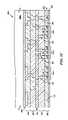
- FIGS. 1A through 1Jare cross-sectional drawings illustrating fabrication of an integrated circuit chip according to a first embodiment of the present invention.
- a first wafer 100 Ais fabricated through pad level.
- Wafer 100 Aincludes a silicon-on-insulator (SOI) substrate 105 A which includes a silicon substrate 110 A, a buried oxide layer (BOX) 115 formed on the silicon substrate and a single-crystal silicon layer 120 formed on the BOX.
- SOIsilicon-on-insulator
- BOXburied oxide layer
- FETsfield effect transistors
- Also formed in silicon layer 120are optional silicon regions 150 .
- a gate dielectric(not shown) and, in one example, polysilicon gates 145 of FETs 130 A.
- silicon regions 150are highly doped N or P-type (between about 1E19 atm/cm 3 and about 1E21 atm/cm 3 in order to reduce the resistance of the contact to less than about 0.5 micro-ohms.
- An optional metal silicide layer 152may be formed on exposed silicon surfaces of source/drains 135 , gates 145 and diffusion contacts 150 prior to formation of a pre-metal dielectric (PMD) layer 155 .
- PMDpre-metal dielectric
- Metal silicidesare formed by deposition of a metal layer on a silicon surface, heating the silicon surface high enough to cause the metal layer to react with the silicon, and then dissolving away any unreacted metal. At this point, the high temperature anneals or rapid thermal anneals (RTAs) required to complete fabrication of FETs 130 A are completed.
- RTAsrapid thermal anneals
- PMD layer 155Formed on top of silicon layer 120 is PMD layer 155 .
- contacts 160are electrically conductive and electrically contact source/drains 135 , gates 145 and silicon contact 150 or other active or passive elements on/in the silicon, such as bipolar junction transistors, thin film resistors, junction capacitors, gate polysilicon capacitors, and the like.
- PMD layer 155 and contacts 160may be considered a pseudo wiring level, connecting the devices on the silicon to the first wiring level.
- contacts 160are formed by a damascene process.
- Formed on PMD layer 155is a first (inter-level dielectric) ILD 165 containing first wiring level conductive damascene wires 170 which may be in electrical contact with contacts 160 .
- first ILD 165Formed on first ILD 165 is a second ILD 180 including electrically conductive dual-damascene wires 180 in electrical contact with wires 170 .
- second ILD 175Formed on second ILD 175 is a third ILD 185 including electrically conductive dual-damascene I/O pads 190 in electrical contact with wires 180 .
- wires 170 , 180 and pads 190may be single damascene wires or pads in combination with single damascene vias.
- a damascene processis one in which wire trenches or via openings are formed in a dielectric layer, an electrical conductor of sufficient thickness to fill the trenches is deposited on a top surface of the dielectric, and a chemical-mechanical-polish (CMP) process is performed to remove excess conductor and make the surface of the conductor co-planar with the surface of the dielectric layer to form damascene wires (or damascene vias).
- CMPchemical-mechanical-polish
- a dual-damascene processis one in which via openings are formed through the entire thickness of a dielectric layer followed by formation of trenches part of the way through the dielectric layer in any given cross-sectional view. All via openings are intersected by integral wire trenches above and by a wire trench below, but not all trenches need intersect a via opening.
- An electrical conductor of sufficient thickness to fill the trenches and via openingis deposited on a top surface of the dielectric and a CMP process is performed to make the surface of the conductor in the trench co-planar with the surface the dielectric layer to form dual-damascene wires and dual-damascene wires having integral dual-damascene vias.
- the etches used in single-damascene and dual damascene processes to form trenchesmay advantageously be reactive ion etches (RIEs).
- RIEsreactive ion etches
- PMD layer 155comprises boro-phospho-silicate glass (BPSG).
- contacts 160comprise a bilayer of titanium/titanium nitride liner and a tungsten core.
- ILD 165 , 175 and 185comprise one or more of silicon dioxide or carbon-doped oxide optionally formed over a layer of silicon nitride, silicon carbo-nitride, or silicon carbo-oxynitride.
- wires 170 and 180 and I/O pads 190comprise a tantalum/tantalum nitride liner and a copper core.
- first ILD 165 , second ILD 175 and third 185independently comprise silicon dioxide (SiO 2 ), silicon nitride (Si 3 N 4 ), silicon carbide (SiC), silicon oxy nitride (SiON), silicon oxy carbide (SiOC), organosilicate glass (SiCOH), plasma-enhanced silicon nitride (PSiN x ) or NBLok (SiC(N,H)).
- first ILD 165 , second ILD 175 and third ILD 185independently comprise a low K (dielectric constant) material, examples of which include but are not limited to hydrogen silsesquioxane polymer (HSQ), methyl silsesquioxane polymer (MSQ), SiLKTM (polyphenylene oligomer) manufactured by Dow Chemical, Midland, Tex., Black DiamondTM (methyl doped silica or SiO x (CH 3 ) y or SiC x O y H y or SiOCH) manufactured by Applied Materials, Santa Clara, Calif., organosilicate glass (SiCOH), and porous SiCOH.
- a low K dielectric materialhas a relative permittivity of about 2.4 or less.
- a passivation layer 195is formed on third ILD 185 and I/O pads 190 and a handle wafer 200 A attached to passivation layer 195 using an adhesive (not shown) or by other methods known in the art.
- the handle waferis thick enough (e.g. 200-1000 microns) to support the silicon wafer during subsequent processing.
- bulk substrate 110 A(see FIG. 1B ) is removed to expose BOX 115 .
- bulk substrate 110 Ais removed by a grinding operation to substantially thin of the bulk substrate operation followed by a chemical etch in a strong base such as aqueous potassium hydroxide to remove the remaining bulk substrate.
- Wafer 100 Bincludes a silicon-on-insulator (SOI) substrate 105 B which includes a silicon substrate 110 B, a buried oxide layer (BOX) 115 formed on the silicon substrate and a single-crystal silicon layer 120 formed on the BOX.
- SOIsilicon-on-insulator
- BOXburied oxide layer
- Formed in silicon layer 120is trench isolation 125 and source/drains 136 and channel regions 141 of field effect transistors (FETs) 130 B.
- FETsfield effect transistors
- Formed over channel regions 141are a gate dielectric (not shown) and, in one example, polysilicon gates 146 of FETs 130 B.
- optional metal silicide layer 152may be formed on exposed silicon surfaces of source/drains 136 and gates 146 prior to formation of pre-metal dielectric (PMD) layer 155 . Formed on top of silicon layer 120 is PMD layer 155 . At this point, the high temperature anneals required to complete fabrication of FETs 130 B are completed.
- PMDpre-metal dielectric
- a handle wafer 200 Battached to PMD layer 155 using an adhesive (not shown) or by other methods known in the art.
- bulk substrate 110 B(see FIG. 1E ) is removed to expose BOX 115 .
- bulk substrate 110 Bis removed by a grinding process to substantially thin of the bulk substrate operation followed by a chemical etch is a strong base such as aqueous potassium hydroxide to remove the remaining bulk substrate.
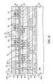
- BOX 115 of first wafer 110 Ais placed over BOX 115 of second wafer 110 B and the first and second wafers are aligned to each other so that when interconnections between devices on wafer 100 A and devices on wafers 110 B are fabricated as described infra, the interconnections and devices will all be in alignment.
- BOX 115 of first wafer 100 Ais bonded to BOX 115 of second wafer 110 B by methods known in the art.
- alignment markswould need to be included on both wafers, designed such that the wafers could be aligned as known in the art.
- handle wafer 200 B(see FIG. 1G ) is removed as known in the art and electrically conductive first type contacts 205 are formed in PMD layer 155 of second wafer 100 B. Contacts 205 extend from the top surface of PMD layer 155 to the silicide (if present) of source/drains 135 and gates 146 (not shown). In one example, contacts 205 are formed by a single damascene process. In one example, contacts 205 comprise a tantalum/tantalum nitride liner and a tungsten core.
- electrically conductive second type contacts 210are formed through PMD layer 155 of second wafer 110 B, trench isolation 125 of second wafer 110 B, BOX of 115 of second wafer 110 B and BOX 115 of first wafer 110 A to source/drains 135 and silicon regions 150 in trench isolation 125 of first wafer 100 A. Contacts 210 may also be formed to channel regions 140 .
- An optional backside metal silicide layer 212may be formed on the exposed surfaces of silicon layer 120 (i.e. source/drains 135 , channel regions 140 and silicon regions 150 ) to further reduce the resistance of the interconnection.
- the temperature of wafers 100 A and 100 B during the heating step of silicide formationis advantageously held to about 400° C. or less.
- metal silicide layer 212comprises nickel silicide.
- contacts 205comprise a tantalum/tantalum nitride liner and a tungsten core.
- a third type contact 215has been formed when a contact 210 is formed abutting (physically and electrically) a contact 205 . This allows a silicon region of silicon layer 120 of second wafer 110 B to be connected to a silicon region of silicon layer 120 of first wafer in a most direct manner and with the shortest physical path possible.
- first, second, and third ( 205 , 210 , and 215 ) types of contactscould be metallized using damascene methods either separately or at the same time.
- First and second type contacts 205 and 210may be fabricated independently in separate operations or simultaneously. When fabricated simultaneously, first and second type contacts may be formed by etching the respective trenches in situ using a single mask or fabricated using various combinations of photolithographic and hard masks and etches to define the trenches separately, followed by a single metal fill and CMP operation.
- first ILD 165including electrically conductive first wiring level damascene wires 170 in electrical contact with contacts 160 .
- second ILD 180including electrically conductive dual-damascene wires 180 in electrical contact with wires 170 .
- third ILD 185including electrically conductive dual-damascene I/O pads 190 in electrical contact with wires 180 .
- a passivation layer 195is formed on third ILD 185 and I/O pads 190 .
- wires 170 , 180 and pads 190 ofmay be single damascene wires in combination with single damascene vias. This completes fabrication of a double wafer 100 C.
- wafers 100 A and 110 BWhile each of wafers 100 A and 110 B has been illustrated with a single contact levels, two wiring levels and a pad level, more or less contact and wiring levels may be fabricated and wafers 100 A and 110 B may be fabricated with different numbers of contact and/or wiring levels.
- Handle wafer 200 Amay be detached from double wafer 100 C at this point in the fabrication process, after further fabrication steps, or after dicing of double wafer 100 C into individual integrated circuits.
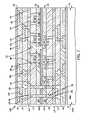
- FIG. 2is a cross-sectional drawing illustrating a first modification to the first embodiment of the present invention.
- the first modification to the first embodiment of the present inventionadds contacts between structures in first wafer 100 A and first level wires 170 first ILD 165 .
- FIG. 2is similar to FIG. 1J , except that a fourth type contact 220 has been fabricated.
- Contact 220extends through PMD layer 155 of second wafer 110 B, trench isolation 125 of second wafer 10 B, BOX of 115 of second wafer 110 B, and BOX 115 of first wafer 110 A and trench isolation 125 of first wafer 100 A.
- Fourth type contacts 220allows direct electrical connection between wires 170 of the first wiring level of second wafer 110 B and contacts 160 of first wafer 110 A.
- contacts 220are formed by a single damascene process.
- contacts 220comprise a titanium/titanium nitride liner and a tungsten core.
- fourth type contacts 220may be formed down to first wires 170 when no contact 160 is provided.
- First, second and fourth type contacts 205 , 210 and 220may be fabricated independently in separate operations or simultaneously. When fabricated simultaneously, first, second and fourth type contacts may be formed by etching the respective trenches in situ using a single mask or fabricated using various combinations of photolithographic and hard masks and etches to define the trenches separately, followed by a single metal fill and CMP operation.
- FIGS. 3A through 3Care cross-sectional drawings illustrating a second modification to the first embodiment of the present invention.
- the second modification to the first embodiment of the present inventionadds landing pads above BOX layer 115 of first wafer 100 A to reduce the critically of the alignment of wafers 100 A and 100 B to each other.
- FIG. 3Ais similar to FIG. 1C except that an inter-wafer dielectric layer 225 is formed over BOX 115 and dual-damascene landing pads 230 are formed in dielectric layer 225 .
- Landing pads 230extend from a top surface of dielectric layer 225 , through dielectric layer 225 and BOX 115 to source/drain 135 and silicon regions 150 . Landing pads 230 may also contact channel regions 140 .
- a silicon oxide layer 235is deposited on top of dielectric layer 225 and landing pads 230 .
- optional backside metal silicide layer 212may be formed on the exposed surfaces of silicon layer 120 (i.e. source/drains 135 , channel regions 140 and silicon regions 150 ) to further reduce the resistance of the interconnection.
- FIG. 3Bis similar to FIG. 1G except silicon oxide layer 235 of first wafer 100 A is bonded to BOX 115 of second wafer 110 B instead of BOX-to-BOX bonding. Fabrication continues in a manner similar to that described supra in reference to FIGS. 1H to 1 J except that in FIG. 3C , the resulting double wafer 100 E includes dielectric layers 225 and 235 and landing pads 230 and contacts 205 and 210 are in direct physical and electrical contact with landing pads 230 rather than in direct physical contact with source/drains 135 , channel regions 140 and silicon regions 150 . Landing pads 230 can be fabricated from refractory metals (Ti/TiN/W) or copper (Ta/TanN/Cu) as described.
- FIGS. 4A through 4Eare cross-sectional drawings illustrating fabrication of an integrated circuit chip according to a second embodiment of the present invention.
- the second embodiment of the present inventionis similar to the first embodiment of the present invention except that the first wafer does not include any wiring levels (i.e. does not include first ILD 165 , second ILD 175 and corresponding wires 270 and 180 and pads 190 . Therefore, in FIG. 4A , a wafer 100 F includes SOI substrate 105 A which includes a silicon bulk substrate 110 A, BOX 115 , single-crystal silicon layer 120 , trench isolation 125 , source/drains 135 and channel regions 140 of FETs 130 A, optional silicon regions 150 gate dielectric (not shown) and gates 145 of FETs 130 A.
- wafer 100 Fmay include electrically conductive contacts interconnecting source/drains 145 , gates 145 and silicon regions 150 .
- a passivation layer 240is formed over PMD 155 .
- passivation layer 240comprises silicon nitride.
- handle wafer 200 Ais attached to passivation layer 240 and in FIG. 4C , bulk silicon substrate 110 A (see FIG. 4B ) is removed as described supra to expose BOX 115 .
- second wafer 100 B(described supra) is attached to first wafer 110 F bonding BOX 115 of first wafer 100 F to BOX 115 of wafer 100 B. Fabrication continues in a manner similar to that described supra in reference to FIGS. 1H to 1J resulting in double wafer 100 G of FIG. 4E .
- FIG. 5a cross-sectional drawing illustrating a modification to the second embodiment of the present invention.
- the modification to the second embodiment of the present inventionis similar to the second modification to the first embodiment in that landing pads are added above BOX layer 115 of a first wafer 100 H (otherwise identical to wafer 100 F of FIG. 4E ) to reduce the critically of the alignment of wafers 100 F and 100 B to each other.
- FIG. 5is similar to FIG. 4E except that a dielectric layer 225 is formed over BOX 115 and dual-damascene landing pads 230 are formed in dielectric layer 225 . Landing pads 230 extend from a top surface of dielectric layer 225 , through dielectric layer 225 and BOX 115 to source/drain 135 and silicon regions 150 .
- Landing pads 230may also contact channel regions 140 .
- a silicon oxide layer 235is deposited on top of dielectric layer 225 and landing pads 230 .
- Wafers 100 His bonded to wafer 110 B by bonding BOX 115 of wafer 100 B to silicon oxide layer 235 of wafer 100 H.
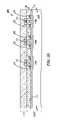
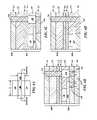
- FIG. 6Ais an orientation view and FIGS. 6B through 6D are cross-section views illustrating alternative methods of contacting the gates of devices according to the various embodiments of the present invention.
- gate 145overlaps source/drains 135 in both the length and width directions.
- Channel region 140has a channel length dimension of L and a channel width dimension of W.
- Source drains 135 and channel region 140are surrounded by trench isolation (not shown).
- electrical connection to gate 145 in first wafer 100 A from second wafer 100 Bis through contact 210 , silicon region 150 , a first contact 160 , wire 170 and a second contact 160 .
- electrical connection to gate 145 in first wafer 100 A from second wafer 100 Bis through contact 210 , silicon region 150 , and an elongated contact 160 .
- electrical connection to gate 145 in first wafer 100 A from second wafer 100 Bis through contact 220 and an elongated contact 160 .
- two wafersfor example 110 A and 100 B
- devicesfor example FETs
- the thermal budgettotal time wafer is at a temperature greater than about 400° C. during fabrication
- the thermal budgetmay be less than that of the second wafer. Examples, of fabrication and device combination possible include, but are not limited to those described in Table I.
- first wafermay be swapped with items listed under the second wafer for any option and that the first wafer may include one or more options and the second wafer may include one or more options, the number of options and the options themselves may be the same or different for the two wafers, provided the items selected for a particular wafer are not mutually exclusive. For example, ⁇ 100> and ⁇ 110> orientation are mutually exclusive.
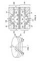
- FIG. 7is an isometric view of an optional alignment of two wafers during fabrication of integrated circuit chips according to the embodiments of the present invention.
- the atoms, which make up the solidare spatially arranged in a periodic fashion called a lattice.
- a crystal latticecontains a volume, which is representative of the entire lattice and is regularly repeated throughout the crystal.
- the directions in a latticeare expressed as a set of three integers with the same relationship as the components of a vector in that direction.
- cubic latticessuch as silicon, that has a diamond crystal lattice
- a body diagonalexists along the [111] direction with the [ ] brackets denoting a specific direction.
- Many directions in a crystal latticeare equivalent by a symmetry transformation, depending upon the arbitrary choice of orientation axes.
- the crystal directions in the cubic lattice [100], [010] and [001]are all crystallographically equivalent.
- a direction and all its equivalent directionsare denoted by ⁇ > brackets.
- the designation of the ⁇ 100> directionincludes the equivalent [100], [010] and [001] positive directions as well as the equivalent negative directions [ ⁇ 100], [0-10] and [00-1].
- Planes in a crystalmay also be identified with a set of three integers. They are used to define a set of parallel planes and each set of integers enclosed in ( ) parentheses identifies a specific plane. For example the proper designation for a plane perpendicular to the [100] direction is (100). Thus, if either a direction or a plane of a cubic lattice is known, its perpendicular counterpart may be quickly determined without calculation. Many planes in a crystal lattice are equivalent by a symmetry transformation, depending upon the arbitrary choice of orientation axes. For example, the (100), (010) and (001) planes are all crystallographically equivalent. A plane and all its equivalent planes are denoted by ⁇ ⁇ parentheses. Thus, the designation of the ⁇ 100 ⁇ plane includes the equivalent (100), (010) and (001) positive planes as well as the equivalent planes ( ⁇ 100), (0-10) and (00-1).
- the mobility of the electrons (inversion carriers) in the channels of N-channel FETs (NFETs)is nearly at its highest in the ⁇ 100 ⁇ plane and significantly lower in the ⁇ 110 ⁇ plane.
- the electron-mobility in the ⁇ 110 ⁇ planeis about half that in the ⁇ 100 ⁇ plane.
- the mobility of holes (inversion carriers) in the channels of P channel FETS (PFETs)is highest in the ⁇ 110 ⁇ plane and significantly lower in the ⁇ 100 ⁇ plane.
- the hole-mobility in the ⁇ 100 ⁇ planeis about less than half that in the ⁇ 110 ⁇ plane.
- wafer 100 Ais aligned to wafer 100 B about a mutual axis CL through the center of each wafer; the [100] direction of wafer 100 A is aligned with the [110] direction of wafer 110 B.
- PFETs 130 Bare formed in wafer 100 B so their channel length is along the [110] direction to maximize PFET inversion carrier mobility while NFETs in wafer 100 A are formed so their channel length is along the [100] direction to maximize NFET inversion carrier mobility.
- While aligning the [100] direction of wafer 100 A with the [110] direction of wafer 100 Bis optional, such alignment orientates the PFETs and NFETs in the same direction (the channel length direction) facilitating alignment of devices in the two wafers.
- FIG. 8is a cross-sectional view of optional fabrication steps during fabrication of integrated circuit chips according to the embodiments of the present invention. Two optional fabrication steps are shown in FIG. 8 .
- FET 130 A of wafer 100 Ais an NFET (source/drains 135 doped N-type, channel region 140 doped P-type) and FET 130 B of wafer 100 B is a PFET (source/drains 136 doped P-type, channel region 141 doped N-type).
- a tensile layer 255 Ais deposited over FET 130 A and a compressive layer 255 B is deposited over FET 130 B.
- the respective tensile and compressive stresses induced in the silicon regions of FETs 130 A and 130 B by respective layers 255 A and 255 Benhance the performance of FETs 130 A and 130 B.
- Suitable materials for layers 255 A and 255 Binclude but are not limited to silicon nitride, silicon carbide, hydrogenated silicon carbide, hydrogenated silicon carbon nitride, hydrogenated silicon oxycarbide, hydrogenated silicon oxy-carbon nitride and combinations thereof in a single layer and combinations of layers thereof.
- the amount of stress appliedis between about 0.5 GPa and 4 GPa.
- Layers 255 A and 255 Bmay also serve as diffusion barrier layers.
- tensile and compressive stressesare introduced into respective FETs 130 A and 130 B by respective dielectric layers 2550 A and 255 B.
- Suitable dielectrics for imparting tensile or compressive stress to FET's 130 A and 130 Binclude silicon nitride, silicon carbide, silicon carbonitride, and the like as known in the art.
- Tensile dielectricsare formed over NFETs and compressive dielectrics over PFETs as is known in the art.
- Metal silicide layers 260 A and 260 Bmay also be used to lower barrier heights and reduce the contact resistance to the source/drains of FETs.
- suitable silicides and their barrier heightsinclude iridium silicide (0.22 eV), platinum silicide (0.26 eV) and palladium silicide (0.4 eV).
- suitable silicides and their barrier heightsinclude hafnium silicide (0.50 eV), titanium silicide (0.60 eV), nickel silicide (0.65 eV) and cobalt silicide (0.65 eV).
- FIG. 9is a flowchart of the methods of fabricating integrated circuit chips according to the embodiments of the present invention.
- an SOI lower wafer(corresponding to wafer 100 A described supra) is fabricated through PMD.
- step 305it is determined if the lower wafer is to be wired. If the lower wafer is to be wired, then in step 310 , the lower wafer is completed through all the ILD levels otherwise the method proceeds to step 315 .
- an optional passivation layeris deposited on the frontside of the lower wafer.
- optional landing padsare formed and a silicon oxide layer deposited.
- a lower handle wafer attached to the frontside of the lower wafer and in step 330 the siliconis removed from the backside of the lower wafer, exposing the BOX of the lower wafer.
- an optional passivation layeris deposited on the BOX. If the optional passivation layer is deposited on the BOX.
- an SOI upper wafer(corresponding to wafer 100 B described supra) is fabricated through PMD.
- an upper lower handle waferattached to the frontside of the upper wafer and in step 345 the silicon is removed from the backside of the upper wafer, exposing the BOX of the upper wafer.
- the lower waferis inverted and the BOX of the upper wafer is placed on the BOX (or the silicon oxide layer if landing pads are utilized) of the lower wafer, the wafers are aligned and then bonded together.
- the upper handle waferis removed.
- step 360contact openings are formed in the PMD of the upper wafer to the devices and FETs (source/drains gates) of the upper wafer.
- step 365a metal silicide is optionally formed and the contact openings filled with an electrically conductive material.
- step 370contact openings are formed through the PMD of the upper wafer and all intervening layers to source/drains of the devices and FETs and other silicon regions of the lower wafer.
- step 375a metal silicide is optionally formed and the contact openings filled with an electrically conductive material.
- step 380contact openings are formed through the PMD of the upper wafer and all intervening layers to the landing pads and/or contracts and/or first level wires of the lower wafer and the openings filled with an electrically conductive material.
- step 385the upper wafer is fabricated though all ILD levels.
- FIG. 10is a flow diagram of a design process used in semiconductor design, manufacturing, and/or test.
- a design flow 400may vary depending on the type of IC being designed.
- a design flow 400 for building an application specific IC (ASIC)may differ from a design flow 400 for designing a standard component.
- Design structure 420is preferably an input to a design process 410 and may come from an IP provider, a core developer, or other design company or may be generated by the operator of the design flow, or from other sources.
- Design structure 420comprises integrated circuit chips 100 A, 100 B, 100 C, 100 D, 100 E, 100 F, 100 G, 100 H, 100 I or combinations thereof in the form of schematics or HDL, a hardware-description language (e.g., Verilog, VHDL, C, etc.).
- Design structure 420may be contained on one or more machine readable medium.
- design structure 420may be a text file or a graphical representation of integrated circuit chips 100 A, 100 B, 100 C, 100 D, 100 E, 100 F, 100 G, 100 H, 100 I or combinations thereof.
- Design process 410preferably synthesizes (or translates) integrated circuit chips 100 A, 100 B, 100 C, 100 D, 100 E, 100 F, 100 G, 100 H, 100 I or combinations thereof into a netlist 480 , where netlist 480 is, for example, a list of wires, transistors, logic gates, control circuits, I/O, models, etc. that describes the connections to other elements and circuits in an integrated circuit design and recorded on at least one of machine readable medium. This may be an iterative process in which netlist 480 is re-synthesized one or more times depending on design specifications and parameters for the circuit.
- Design process 410may include using a variety of inputs; for example, inputs from library elements 430 which may house a set of commonly used elements, circuits, and devices, including models, layouts, and symbolic representations, for a given manufacturing technology (e.g., different technology nodes, 32 nm, 45 nm, 40 nm, etc.), design specifications 440 , characterization data 450 , verification data 460 , design rules 470 , and test data files 485 (which may include test patterns and other testing information). Design process 410 may further include, for example, standard circuit design processes such as timing analysis, verification, design rule checking, place and route operations, etc.
- One of ordinary skill in the art of integrated circuit designcan appreciate the extent of possible electronic design automation tools and applications used in design process 410 without deviating from the scope and spirit of the invention.
- the design structure of the inventionis not limited to any specific design flow.
- design process 410preferably translates integrated circuit chips 100 A, 100 B, 100 C, 100 D, 100 E, 100 F, 100 G, 100 H, 100 I or combinations thereof, along with the rest of the integrated circuit design (if applicable), into a final design structure 440 (e.g., information stored in a GDS storage medium).
- Final design structure 440may comprise information such as, for example, test data files, design content files, manufacturing data, layout parameters, wires, levels of metal, vias, shapes, test data, data for routing through the manufacturing line, and any other data required by a semiconductor manufacturer to produce integrated circuit chips 100 A, 100 B, 100 C, 100 D, 100 E, 100 F, 100 G, 100 H, 100 I or combinations thereof.
- Final design structure 490may then proceed to a stage 495 where, for example, final design structure 490 : proceeds to tape-out, is released to manufacturing, is sent to another design house or is sent back to the customer.
- the embodiments of the present inventionprovide integrated circuit chips, methods of fabricating integrated circuit chips and design structures of integrated circuit chips, wherein the fabrication process may be adjusted to enhance the performance of different types of devices in a cost effective manner.
Landscapes
- Engineering & Computer Science (AREA)
- Microelectronics & Electronic Packaging (AREA)
- Computer Hardware Design (AREA)
- Power Engineering (AREA)
- Physics & Mathematics (AREA)
- General Physics & Mathematics (AREA)
- Condensed Matter Physics & Semiconductors (AREA)
- Manufacturing & Machinery (AREA)
- Theoretical Computer Science (AREA)
- Computer Networks & Wireless Communication (AREA)
- Evolutionary Computation (AREA)
- Geometry (AREA)
- General Engineering & Computer Science (AREA)
- Internal Circuitry In Semiconductor Integrated Circuit Devices (AREA)
Abstract
Description
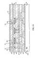
| TABLE I | |||
| SECOND | |||
| OPTION | WAFER | ||
| 1 | NFETs | PFETs | |
| 2 | FETs in Tension | FETs in | |
| Compression | |||
| 3 | Logic Circuits | Memory Circuits | |
| 4 | High Threshold | Low Threshold | |
| (VT) FETs | (VT) FETs | ||
| 5 | Thick Gate | Thin Gate | |
| Dielectric FETs | Dielectric FETs | ||
| 6 | Analog | Digital Circuits | |
| 7 | <100> Silicon | <110> Silicon | |
| Wafer | Wafer | ||
| 8 | Thermal Budget 2 | ||
| 9 | CMOS FETS | Bipolar | |
| Transistors | |||
Claims (16)
Priority Applications (3)
| Application Number | Priority Date | Filing Date | Title |
|---|---|---|---|
| US11/939,612US8013342B2 (en) | 2007-11-14 | 2007-11-14 | Double-sided integrated circuit chips |
| US13/192,608US8471306B2 (en) | 2006-05-16 | 2011-07-28 | Double-sided integrated circuit chips |
| US13/783,438US8689152B2 (en) | 2006-05-16 | 2013-03-04 | Double-sided integrated circuit chips |
Applications Claiming Priority (1)
| Application Number | Priority Date | Filing Date | Title |
|---|---|---|---|
| US11/939,612US8013342B2 (en) | 2007-11-14 | 2007-11-14 | Double-sided integrated circuit chips |
Related Parent Applications (1)
| Application Number | Title | Priority Date | Filing Date |
|---|---|---|---|
| US11/383,586Continuation-In-PartUS7670927B2 (en) | 2006-05-16 | 2006-05-16 | Double-sided integrated circuit chips |
Related Child Applications (2)
| Application Number | Title | Priority Date | Filing Date |
|---|---|---|---|
| US13/192,608DivisionUS8471306B2 (en) | 2006-05-16 | 2011-07-28 | Double-sided integrated circuit chips |
| US13/192,606DivisionUS8571163B2 (en) | 2006-02-28 | 2011-07-28 | Monitoring method and monitoring program for boiling water reactor, and acoustic damping method for boiling water reactor |
Publications (2)
| Publication Number | Publication Date |
|---|---|
| US20090121260A1 US20090121260A1 (en) | 2009-05-14 |
| US8013342B2true US8013342B2 (en) | 2011-09-06 |
Family
ID=40622894
Family Applications (3)
| Application Number | Title | Priority Date | Filing Date |
|---|---|---|---|
| US11/939,612Expired - Fee RelatedUS8013342B2 (en) | 2006-05-16 | 2007-11-14 | Double-sided integrated circuit chips |
| US13/192,608Expired - Fee RelatedUS8471306B2 (en) | 2006-05-16 | 2011-07-28 | Double-sided integrated circuit chips |
| US13/783,438ActiveUS8689152B2 (en) | 2006-05-16 | 2013-03-04 | Double-sided integrated circuit chips |
Family Applications After (2)
| Application Number | Title | Priority Date | Filing Date |
|---|---|---|---|
| US13/192,608Expired - Fee RelatedUS8471306B2 (en) | 2006-05-16 | 2011-07-28 | Double-sided integrated circuit chips |
| US13/783,438ActiveUS8689152B2 (en) | 2006-05-16 | 2013-03-04 | Double-sided integrated circuit chips |
Country Status (1)
| Country | Link |
|---|---|
| US (3) | US8013342B2 (en) |
Cited By (12)
| Publication number | Priority date | Publication date | Assignee | Title |
|---|---|---|---|---|
| US20110140223A1 (en)* | 2009-12-11 | 2011-06-16 | Oki Semiconductor Co., Ltd. | Light detecting apparatus and method of manufacturing same |
| US20120153359A1 (en)* | 2010-01-08 | 2012-06-21 | International Business Machines Corporation | Nickel-silicide formation with differential pt composition |
| US8421126B2 (en) | 2006-05-16 | 2013-04-16 | International Business Machines Corporation | Double-sided integrated circuit chips |
| US8471306B2 (en) | 2006-05-16 | 2013-06-25 | International Business Machines Corporation | Double-sided integrated circuit chips |
| US8686342B2 (en) | 2012-04-09 | 2014-04-01 | Omnivision Technologies, Inc. | Double-sided image sensor formed on a single semiconductor wafer die |
| US9368468B2 (en) | 2009-07-15 | 2016-06-14 | Qualcomm Switch Corp. | Thin integrated circuit chip-on-board assembly |
| US9390974B2 (en) | 2012-12-21 | 2016-07-12 | Qualcomm Incorporated | Back-to-back stacked integrated circuit assembly and method of making |
| US9466719B2 (en) | 2009-07-15 | 2016-10-11 | Qualcomm Incorporated | Semiconductor-on-insulator with back side strain topology |
| US9496227B2 (en) | 2009-07-15 | 2016-11-15 | Qualcomm Incorporated | Semiconductor-on-insulator with back side support layer |
| US9515181B2 (en) | 2014-08-06 | 2016-12-06 | Qualcomm Incorporated | Semiconductor device with self-aligned back side features |
| US9748272B2 (en) | 2009-07-15 | 2017-08-29 | Qualcomm Incorporated | Semiconductor-on-insulator with back side strain inducing material |
| US20180122733A1 (en)* | 2016-06-30 | 2018-05-03 | Unimicron Technology Corp. | Method for manufacturing circuit redistribution structure |
Families Citing this family (16)
| Publication number | Priority date | Publication date | Assignee | Title |
|---|---|---|---|---|
| US20090289284A1 (en)* | 2008-05-23 | 2009-11-26 | Chartered Semiconductor Manufacturing, Ltd. | High shrinkage stress silicon nitride (SiN) layer for NFET improvement |
| US8748288B2 (en) | 2010-02-05 | 2014-06-10 | International Business Machines Corporation | Bonded structure with enhanced adhesion strength |
| EP2597670B1 (en)* | 2010-03-31 | 2016-03-30 | EV Group E. Thallner GmbH | Method for permanently connecting two metal surfaces |
| US8341588B2 (en)* | 2010-10-04 | 2012-12-25 | International Business Machines Corporation | Semiconductor layer forming method and structure |
| US8921992B2 (en)* | 2013-03-14 | 2014-12-30 | Raytheon Company | Stacked wafer with coolant channels |
| US9177956B2 (en)* | 2013-07-31 | 2015-11-03 | Globalfoundries Inc. | Field effect transistor (FET) with self-aligned contacts, integrated circuit (IC) chip and method of manufacture |
| US9929133B2 (en)* | 2013-08-27 | 2018-03-27 | Taiwan Semiconductor Manufacturing Company Limited | Semiconductor logic circuits fabricated using multi-layer structures |
| US10163897B2 (en) | 2013-11-15 | 2018-12-25 | Taiwan Semiconductor Manufacturing Co., Ltd. | Inter-level connection for multi-layer structures |
| EP3155654A4 (en)* | 2014-06-16 | 2018-06-27 | Intel Corporation | Silicon die with integrated high voltage devices |
| TW201724510A (en) | 2015-05-15 | 2017-07-01 | 西凱渥資訊處理科技公司 | RF isolation using substrate openings |
| US9847293B1 (en)* | 2016-08-18 | 2017-12-19 | Qualcomm Incorporated | Utilization of backside silicidation to form dual side contacted capacitor |
| US9837302B1 (en)* | 2016-08-26 | 2017-12-05 | Qualcomm Incorporated | Methods of forming a device having semiconductor devices on two sides of a buried dielectric layer |
| US10367031B2 (en)* | 2016-09-13 | 2019-07-30 | Imec Vzw | Sequential integration process |
| DE102018107077A1 (en) | 2017-08-30 | 2019-02-28 | Taiwan Semiconductor Manufacturing Co., Ltd. | Merged column structures and methods of generating layout diagrams therefrom |
| US10515178B2 (en)* | 2017-08-30 | 2019-12-24 | Taiwan Semiconductor Manufacturing Company, Ltd. | Merged pillar structures and method of generating layout diagram of same |
| US20230026676A1 (en)* | 2021-07-23 | 2023-01-26 | Taiwan Semiconductor Manufacturing Company, Ltd. | Semiconductor device structure and method of formation |
Citations (24)
| Publication number | Priority date | Publication date | Assignee | Title |
|---|---|---|---|---|
| US4612083A (en) | 1984-07-20 | 1986-09-16 | Nec Corporation | Process of fabricating three-dimensional semiconductor device |
| US4939568A (en) | 1986-03-20 | 1990-07-03 | Fujitsu Limited | Three-dimensional integrated circuit and manufacturing method thereof |
| US5825696A (en) | 1993-12-03 | 1998-10-20 | Mitsubishi Denki Kabushiki Kaisha | Semiconductor memory device including an SOI substrate |
| US5889302A (en)* | 1997-04-21 | 1999-03-30 | Advanced Micro Devices, Inc. | Multilayer floating gate field effect transistor structure for use in integrated circuit devices |
| US6166438A (en) | 1994-07-12 | 2000-12-26 | Sun Microsystems, Inc. | Ultrathin electronics using stacked layers and interconnect vias |
| US6355501B1 (en) | 2000-09-21 | 2002-03-12 | International Business Machines Corporation | Three-dimensional chip stacking assembly |
| US6410371B1 (en) | 2001-02-26 | 2002-06-25 | Advanced Micro Devices, Inc. | Method of fabrication of semiconductor-on-insulator (SOI) wafer having a Si/SiGe/Si active layer |
| US6573172B1 (en) | 2002-09-16 | 2003-06-03 | Advanced Micro Devices, Inc. | Methods for improving carrier mobility of PMOS and NMOS devices |
| US20030129829A1 (en) | 2002-01-08 | 2003-07-10 | David Greenlaw | Three-dimensional integrated semiconductor devices |
| US20040048459A1 (en) | 2002-04-11 | 2004-03-11 | Robert Patti | Interlocking conductor method for bonding wafers to produce stacked integrated circuits |
| US20040105300A1 (en) | 2002-11-29 | 2004-06-03 | Chuang Ching-Te K. | Reduced integrated circuit chip leakage and method of reducing leakage |
| US6762076B2 (en) | 2002-02-20 | 2004-07-13 | Intel Corporation | Process of vertically stacking multiple wafers supporting different active integrated circuit (IC) devices |
| US20040144979A1 (en) | 2002-10-03 | 2004-07-29 | Arup Bhattacharyya | High performance three-dimensional TFT-based CMOS inverters, and computer systems utilizing such novel CMOS inverters |
| US20040188819A1 (en) | 2003-03-31 | 2004-09-30 | Farnworth Warren M. | Wafer level methods for fabricating multi-dice chip scale semiconductor components |
| US6812127B2 (en) | 2000-11-29 | 2004-11-02 | Renesas Technology Corp. | Method of forming semiconductor device including silicon oxide with fluorine, embedded wiring layer, via holes, and wiring grooves |
| US6815278B1 (en) | 2003-08-25 | 2004-11-09 | International Business Machines Corporation | Ultra-thin silicon-on-insulator and strained-silicon-direct-on-insulator with hybrid crystal orientations |
| US6821826B1 (en) | 2003-09-30 | 2004-11-23 | International Business Machines Corporation | Three dimensional CMOS integrated circuits having device layers built on different crystal oriented wafers |
| US6830962B1 (en) | 2003-08-05 | 2004-12-14 | International Business Machines Corporation | Self-aligned SOI with different crystal orientation using wafer bonding and SIMOX processes |
| US20050093104A1 (en) | 2003-10-29 | 2005-05-05 | International Business Machines Corporation | CMOS on hybrid substrate with different crystal orientations using silicon-to-silicon direct wafer bonding |
| US20050269680A1 (en) | 2004-06-08 | 2005-12-08 | Min-Chih Hsuan | System-in-package (SIP) structure and fabrication thereof |
| US20050275017A1 (en)* | 2004-05-28 | 2005-12-15 | Pozder Scott K | Separately strained N-channel and P-channel transistors |
| US20060068557A1 (en) | 2003-08-05 | 2006-03-30 | Fujitsu Limited | Semiconductor device and method for fabricating the same |
| US20060226491A1 (en)* | 2005-04-06 | 2006-10-12 | International Business Machines Corporation | Inverted multilayer semiconductor device assembly |
| US7320115B2 (en)* | 2005-07-12 | 2008-01-15 | Taiwan Semiconductor Manufacturing Co., Ltd. | Method for identifying a physical failure location on an integrated circuit |
Family Cites Families (5)
| Publication number | Priority date | Publication date | Assignee | Title |
|---|---|---|---|---|
| US5837427A (en)* | 1996-04-30 | 1998-11-17 | Samsung Electro-Mechanics Co Co., Ltd. | Method for manufacturing build-up multi-layer printed circuit board |
| US6949067B1 (en)* | 2004-05-11 | 2005-09-27 | Dann Jeffrey A | Device and method for enhancing female sexual stimulation |
| US7312487B2 (en) | 2004-08-16 | 2007-12-25 | International Business Machines Corporation | Three dimensional integrated circuit |
| US8013342B2 (en) | 2007-11-14 | 2011-09-06 | International Business Machines Corporation | Double-sided integrated circuit chips |
| US7670927B2 (en) | 2006-05-16 | 2010-03-02 | International Business Machines Corporation | Double-sided integrated circuit chips |
- 2007
- 2007-11-14USUS11/939,612patent/US8013342B2/ennot_activeExpired - Fee Related
- 2011
- 2011-07-28USUS13/192,608patent/US8471306B2/ennot_activeExpired - Fee Related
- 2013
- 2013-03-04USUS13/783,438patent/US8689152B2/enactiveActive
Patent Citations (26)
| Publication number | Priority date | Publication date | Assignee | Title |
|---|---|---|---|---|
| US4612083A (en) | 1984-07-20 | 1986-09-16 | Nec Corporation | Process of fabricating three-dimensional semiconductor device |
| US4939568A (en) | 1986-03-20 | 1990-07-03 | Fujitsu Limited | Three-dimensional integrated circuit and manufacturing method thereof |
| US5825696A (en) | 1993-12-03 | 1998-10-20 | Mitsubishi Denki Kabushiki Kaisha | Semiconductor memory device including an SOI substrate |
| US6166438A (en) | 1994-07-12 | 2000-12-26 | Sun Microsystems, Inc. | Ultrathin electronics using stacked layers and interconnect vias |
| US5889302A (en)* | 1997-04-21 | 1999-03-30 | Advanced Micro Devices, Inc. | Multilayer floating gate field effect transistor structure for use in integrated circuit devices |
| US6355501B1 (en) | 2000-09-21 | 2002-03-12 | International Business Machines Corporation | Three-dimensional chip stacking assembly |
| US6812127B2 (en) | 2000-11-29 | 2004-11-02 | Renesas Technology Corp. | Method of forming semiconductor device including silicon oxide with fluorine, embedded wiring layer, via holes, and wiring grooves |
| US6410371B1 (en) | 2001-02-26 | 2002-06-25 | Advanced Micro Devices, Inc. | Method of fabrication of semiconductor-on-insulator (SOI) wafer having a Si/SiGe/Si active layer |
| US20030129829A1 (en) | 2002-01-08 | 2003-07-10 | David Greenlaw | Three-dimensional integrated semiconductor devices |
| US6943067B2 (en) | 2002-01-08 | 2005-09-13 | Advanced Micro Devices, Inc. | Three-dimensional integrated semiconductor devices |
| US6762076B2 (en) | 2002-02-20 | 2004-07-13 | Intel Corporation | Process of vertically stacking multiple wafers supporting different active integrated circuit (IC) devices |
| US20040048459A1 (en) | 2002-04-11 | 2004-03-11 | Robert Patti | Interlocking conductor method for bonding wafers to produce stacked integrated circuits |
| US6573172B1 (en) | 2002-09-16 | 2003-06-03 | Advanced Micro Devices, Inc. | Methods for improving carrier mobility of PMOS and NMOS devices |
| US20040144979A1 (en) | 2002-10-03 | 2004-07-29 | Arup Bhattacharyya | High performance three-dimensional TFT-based CMOS inverters, and computer systems utilizing such novel CMOS inverters |
| US20040105300A1 (en) | 2002-11-29 | 2004-06-03 | Chuang Ching-Te K. | Reduced integrated circuit chip leakage and method of reducing leakage |
| US20040188819A1 (en) | 2003-03-31 | 2004-09-30 | Farnworth Warren M. | Wafer level methods for fabricating multi-dice chip scale semiconductor components |
| US6830962B1 (en) | 2003-08-05 | 2004-12-14 | International Business Machines Corporation | Self-aligned SOI with different crystal orientation using wafer bonding and SIMOX processes |
| US20050070077A1 (en) | 2003-08-05 | 2005-03-31 | International Business Machines Corporation | Self-aligned SOI with different crystal orientation using WAFER bonding and SIMOX processes |
| US20060068557A1 (en) | 2003-08-05 | 2006-03-30 | Fujitsu Limited | Semiconductor device and method for fabricating the same |
| US6815278B1 (en) | 2003-08-25 | 2004-11-09 | International Business Machines Corporation | Ultra-thin silicon-on-insulator and strained-silicon-direct-on-insulator with hybrid crystal orientations |
| US6821826B1 (en) | 2003-09-30 | 2004-11-23 | International Business Machines Corporation | Three dimensional CMOS integrated circuits having device layers built on different crystal oriented wafers |
| US20050093104A1 (en) | 2003-10-29 | 2005-05-05 | International Business Machines Corporation | CMOS on hybrid substrate with different crystal orientations using silicon-to-silicon direct wafer bonding |
| US20050275017A1 (en)* | 2004-05-28 | 2005-12-15 | Pozder Scott K | Separately strained N-channel and P-channel transistors |
| US20050269680A1 (en) | 2004-06-08 | 2005-12-08 | Min-Chih Hsuan | System-in-package (SIP) structure and fabrication thereof |
| US20060226491A1 (en)* | 2005-04-06 | 2006-10-12 | International Business Machines Corporation | Inverted multilayer semiconductor device assembly |
| US7320115B2 (en)* | 2005-07-12 | 2008-01-15 | Taiwan Semiconductor Manufacturing Co., Ltd. | Method for identifying a physical failure location on an integrated circuit |
Non-Patent Citations (5)
| Title |
|---|
| Notice of Allowance (Mail Date Mar. 22, 2011) for U.S. Appl. No. 12/612,957, filed Nov. 5, 2009; Confirmation No. 5440. |
| Notice of Allowance (Mail Date Oct. 8, 2009) for U.S. Appl. No. 11/383,586, filed May 16, 2006, First Named Inventor Kerry Bernstein; Confirmation No. 7897. |
| Office Action (Mail Date Dec. 23, 2010) for U.S. Appl. No. 12/612,957, filed Nov. 5, 2009; Confirmation No. 5440. |
| Office Action (Mail Date May 14, 2009) for U.S. Appl. No. 11/383,586, filed Jun. 15, 2006; Confirmation No. 7897. |
| U.S. Appl. No. 12/612,957, filed Nov. 5, 2009, First Named Inventor Kerry Bernstein et al.; Confirmation No. 5440. |
Cited By (19)
| Publication number | Priority date | Publication date | Assignee | Title |
|---|---|---|---|---|
| US8421126B2 (en) | 2006-05-16 | 2013-04-16 | International Business Machines Corporation | Double-sided integrated circuit chips |
| US8689152B2 (en) | 2006-05-16 | 2014-04-01 | International Business Machines Corporation | Double-sided integrated circuit chips |
| US8471306B2 (en) | 2006-05-16 | 2013-06-25 | International Business Machines Corporation | Double-sided integrated circuit chips |
| US9368468B2 (en) | 2009-07-15 | 2016-06-14 | Qualcomm Switch Corp. | Thin integrated circuit chip-on-board assembly |
| US9748272B2 (en) | 2009-07-15 | 2017-08-29 | Qualcomm Incorporated | Semiconductor-on-insulator with back side strain inducing material |
| US10217822B2 (en) | 2009-07-15 | 2019-02-26 | Qualcomm Incorporated | Semiconductor-on-insulator with back side heat dissipation |
| US9412644B2 (en) | 2009-07-15 | 2016-08-09 | Qualcomm Incorporated | Integrated circuit assembly and method of making |
| US9466719B2 (en) | 2009-07-15 | 2016-10-11 | Qualcomm Incorporated | Semiconductor-on-insulator with back side strain topology |
| US9496227B2 (en) | 2009-07-15 | 2016-11-15 | Qualcomm Incorporated | Semiconductor-on-insulator with back side support layer |
| US8319304B2 (en)* | 2009-12-11 | 2012-11-27 | Lapis Semiconductor Co., Ltd. | Light detecting apparatus |
| US20110140223A1 (en)* | 2009-12-11 | 2011-06-16 | Oki Semiconductor Co., Ltd. | Light detecting apparatus and method of manufacturing same |
| US8637925B2 (en)* | 2010-01-08 | 2014-01-28 | International Business Machines Corporation | Nickel-silicide formation with differential Pt composition |
| US20120153359A1 (en)* | 2010-01-08 | 2012-06-21 | International Business Machines Corporation | Nickel-silicide formation with differential pt composition |
| US8686342B2 (en) | 2012-04-09 | 2014-04-01 | Omnivision Technologies, Inc. | Double-sided image sensor formed on a single semiconductor wafer die |
| US9576937B2 (en) | 2012-12-21 | 2017-02-21 | Qualcomm Incorporated | Back-to-back stacked integrated circuit assembly |
| US9390974B2 (en) | 2012-12-21 | 2016-07-12 | Qualcomm Incorporated | Back-to-back stacked integrated circuit assembly and method of making |
| US9515181B2 (en) | 2014-08-06 | 2016-12-06 | Qualcomm Incorporated | Semiconductor device with self-aligned back side features |
| US20180122733A1 (en)* | 2016-06-30 | 2018-05-03 | Unimicron Technology Corp. | Method for manufacturing circuit redistribution structure |
| US10083901B2 (en)* | 2016-06-30 | 2018-09-25 | Unimicron Technology Corp. | Method for manufacturing circuit redistribution structure |
Also Published As
| Publication number | Publication date |
|---|---|
| US20090121260A1 (en) | 2009-05-14 |
| US20110302542A1 (en) | 2011-12-08 |
| US20130179853A1 (en) | 2013-07-11 |
| US8471306B2 (en) | 2013-06-25 |
| US8689152B2 (en) | 2014-04-01 |
Similar Documents
| Publication | Publication Date | Title |
|---|---|---|
| US8013342B2 (en) | Double-sided integrated circuit chips | |
| US8421126B2 (en) | Double-sided integrated circuit chips | |
| US20240332183A1 (en) | Direct bonding on buried power rails | |
| US20230275156A1 (en) | Semiconductor device with metal cap on gate | |
| US10847418B2 (en) | Formation method of damascene structure | |
| US7939914B2 (en) | Dual wired integrated circuit chips | |
| CN105340071B (en) | There is the semiconductor on insulator integrated circuit of interconnection below insulator | |
| TWI707440B (en) | Redistribution layer metallic structure and method | |
| WO2020018471A1 (en) | Thermal extraction of single layer transfer integrated circuits | |
| US9905633B1 (en) | Structure and formation method of semiconductor device structure | |
| CN107210285B (en) | Integrated circuit assembly with Faraday cage | |
| WO2023241932A1 (en) | Multiple critical dimension power rail | |
| US20090121287A1 (en) | Dual wired integrated circuit chips | |
| US20250096128A1 (en) | Bottom contact jumpers for stacked field effect transistor semiconductors | |
| US20250301785A1 (en) | Cross-couple connect in stacked field effect transistor semiconductors | |
| TWI798887B (en) | Semiconductor device with air gap below landing pad and method for preparing the same | |
| US20200194459A1 (en) | Semiconductor devices and methods for fabricating the same |
Legal Events
| Date | Code | Title | Description |
|---|---|---|---|
| AS | Assignment | Owner name:INTERNATIONAL BUSINESS MACHINES CORPORATION, NEW Y Free format text:ASSIGNMENT OF ASSIGNORS INTEREST;ASSIGNORS:BERNSTEIN, KERRY;DALTON, TIMOTHY JOSEPH;GAMBINO, JEFFREY PETER;AND OTHERS;REEL/FRAME:020107/0686;SIGNING DATES FROM 20071105 TO 20071113 Owner name:INTERNATIONAL BUSINESS MACHINES CORPORATION, NEW Y Free format text:ASSIGNMENT OF ASSIGNORS INTEREST;ASSIGNORS:BERNSTEIN, KERRY;DALTON, TIMOTHY JOSEPH;GAMBINO, JEFFREY PETER;AND OTHERS;SIGNING DATES FROM 20071105 TO 20071113;REEL/FRAME:020107/0686 | |
| STCF | Information on status: patent grant | Free format text:PATENTED CASE | |
| FPAY | Fee payment | Year of fee payment:4 | |
| AS | Assignment | Owner name:GLOBALFOUNDRIES U.S. 2 LLC, NEW YORK Free format text:ASSIGNMENT OF ASSIGNORS INTEREST;ASSIGNOR:INTERNATIONAL BUSINESS MACHINES CORPORATION;REEL/FRAME:036550/0001 Effective date:20150629 | |
| AS | Assignment | Owner name:GLOBALFOUNDRIES INC., CAYMAN ISLANDS Free format text:ASSIGNMENT OF ASSIGNORS INTEREST;ASSIGNORS:GLOBALFOUNDRIES U.S. 2 LLC;GLOBALFOUNDRIES U.S. INC.;REEL/FRAME:036779/0001 Effective date:20150910 | |
| AS | Assignment | Owner name:WILMINGTON TRUST, NATIONAL ASSOCIATION, DELAWARE Free format text:SECURITY AGREEMENT;ASSIGNOR:GLOBALFOUNDRIES INC.;REEL/FRAME:049490/0001 Effective date:20181127 | |
| FEPP | Fee payment procedure | Free format text:MAINTENANCE FEE REMINDER MAILED (ORIGINAL EVENT CODE: REM.); ENTITY STATUS OF PATENT OWNER: LARGE ENTITY | |
| LAPS | Lapse for failure to pay maintenance fees | Free format text:PATENT EXPIRED FOR FAILURE TO PAY MAINTENANCE FEES (ORIGINAL EVENT CODE: EXP.); ENTITY STATUS OF PATENT OWNER: LARGE ENTITY | |
| STCH | Information on status: patent discontinuation | Free format text:PATENT EXPIRED DUE TO NONPAYMENT OF MAINTENANCE FEES UNDER 37 CFR 1.362 | |
| FP | Lapsed due to failure to pay maintenance fee | Effective date:20190906 | |
| AS | Assignment | Owner name:GLOBALFOUNDRIES INC., CAYMAN ISLANDS Free format text:RELEASE BY SECURED PARTY;ASSIGNOR:WILMINGTON TRUST, NATIONAL ASSOCIATION;REEL/FRAME:054636/0001 Effective date:20201117 | |
| AS | Assignment | Owner name:GLOBALFOUNDRIES U.S. INC., NEW YORK Free format text:RELEASE BY SECURED PARTY;ASSIGNOR:WILMINGTON TRUST, NATIONAL ASSOCIATION;REEL/FRAME:056987/0001 Effective date:20201117 |