US8013332B2 - Portable memory devices - Google Patents
Portable memory devicesDownload PDFInfo
- Publication number
- US8013332B2 US8013332B2US11/551,423US55142306AUS8013332B2US 8013332 B2US8013332 B2US 8013332B2US 55142306 AUS55142306 AUS 55142306AUS 8013332 B2US8013332 B2US 8013332B2
- Authority
- US
- United States
- Prior art keywords
- circuit board
- recited
- memory card
- contacts
- test contacts
- Prior art date
- Legal status (The legal status is an assumption and is not a legal conclusion. Google has not performed a legal analysis and makes no representation as to the accuracy of the status listed.)
- Active, expires
Links
Images


Classifications
- H—ELECTRICITY
- H05—ELECTRIC TECHNIQUES NOT OTHERWISE PROVIDED FOR
- H05K—PRINTED CIRCUITS; CASINGS OR CONSTRUCTIONAL DETAILS OF ELECTRIC APPARATUS; MANUFACTURE OF ASSEMBLAGES OF ELECTRICAL COMPONENTS
- H05K3/00—Apparatus or processes for manufacturing printed circuits
- H05K3/22—Secondary treatment of printed circuits
- H05K3/28—Applying non-metallic protective coatings
- H—ELECTRICITY
- H01—ELECTRIC ELEMENTS
- H01L—SEMICONDUCTOR DEVICES NOT COVERED BY CLASS H10
- H01L23/00—Details of semiconductor or other solid state devices
- H01L23/58—Structural electrical arrangements for semiconductor devices not otherwise provided for, e.g. in combination with batteries
- H01L23/60—Protection against electrostatic charges or discharges, e.g. Faraday shields
- H—ELECTRICITY
- H05—ELECTRIC TECHNIQUES NOT OTHERWISE PROVIDED FOR
- H05K—PRINTED CIRCUITS; CASINGS OR CONSTRUCTIONAL DETAILS OF ELECTRIC APPARATUS; MANUFACTURE OF ASSEMBLAGES OF ELECTRICAL COMPONENTS
- H05K1/00—Printed circuits
- H05K1/02—Details
- H05K1/0266—Marks, test patterns or identification means
- H05K1/0268—Marks, test patterns or identification means for electrical inspection or testing
- H—ELECTRICITY
- H01—ELECTRIC ELEMENTS
- H01L—SEMICONDUCTOR DEVICES NOT COVERED BY CLASS H10
- H01L2224/00—Indexing scheme for arrangements for connecting or disconnecting semiconductor or solid-state bodies and methods related thereto as covered by H01L24/00
- H01L2224/01—Means for bonding being attached to, or being formed on, the surface to be connected, e.g. chip-to-package, die-attach, "first-level" interconnects; Manufacturing methods related thereto
- H01L2224/26—Layer connectors, e.g. plate connectors, solder or adhesive layers; Manufacturing methods related thereto
- H01L2224/31—Structure, shape, material or disposition of the layer connectors after the connecting process
- H01L2224/32—Structure, shape, material or disposition of the layer connectors after the connecting process of an individual layer connector
- H01L2224/321—Disposition
- H01L2224/32135—Disposition the layer connector connecting between different semiconductor or solid-state bodies, i.e. chip-to-chip
- H01L2224/32145—Disposition the layer connector connecting between different semiconductor or solid-state bodies, i.e. chip-to-chip the bodies being stacked
- H—ELECTRICITY
- H01—ELECTRIC ELEMENTS
- H01L—SEMICONDUCTOR DEVICES NOT COVERED BY CLASS H10
- H01L2224/00—Indexing scheme for arrangements for connecting or disconnecting semiconductor or solid-state bodies and methods related thereto as covered by H01L24/00
- H01L2224/01—Means for bonding being attached to, or being formed on, the surface to be connected, e.g. chip-to-package, die-attach, "first-level" interconnects; Manufacturing methods related thereto
- H01L2224/26—Layer connectors, e.g. plate connectors, solder or adhesive layers; Manufacturing methods related thereto
- H01L2224/31—Structure, shape, material or disposition of the layer connectors after the connecting process
- H01L2224/32—Structure, shape, material or disposition of the layer connectors after the connecting process of an individual layer connector
- H01L2224/321—Disposition
- H01L2224/32151—Disposition the layer connector connecting between a semiconductor or solid-state body and an item not being a semiconductor or solid-state body, e.g. chip-to-substrate, chip-to-passive
- H01L2224/32221—Disposition the layer connector connecting between a semiconductor or solid-state body and an item not being a semiconductor or solid-state body, e.g. chip-to-substrate, chip-to-passive the body and the item being stacked
- H01L2224/32225—Disposition the layer connector connecting between a semiconductor or solid-state body and an item not being a semiconductor or solid-state body, e.g. chip-to-substrate, chip-to-passive the body and the item being stacked the item being non-metallic, e.g. insulating substrate with or without metallisation
- H—ELECTRICITY
- H01—ELECTRIC ELEMENTS
- H01L—SEMICONDUCTOR DEVICES NOT COVERED BY CLASS H10
- H01L2224/00—Indexing scheme for arrangements for connecting or disconnecting semiconductor or solid-state bodies and methods related thereto as covered by H01L24/00
- H01L2224/01—Means for bonding being attached to, or being formed on, the surface to be connected, e.g. chip-to-package, die-attach, "first-level" interconnects; Manufacturing methods related thereto
- H01L2224/42—Wire connectors; Manufacturing methods related thereto
- H01L2224/47—Structure, shape, material or disposition of the wire connectors after the connecting process
- H01L2224/48—Structure, shape, material or disposition of the wire connectors after the connecting process of an individual wire connector
- H01L2224/4805—Shape
- H01L2224/4809—Loop shape
- H01L2224/48091—Arched
- H—ELECTRICITY
- H01—ELECTRIC ELEMENTS
- H01L—SEMICONDUCTOR DEVICES NOT COVERED BY CLASS H10
- H01L2224/00—Indexing scheme for arrangements for connecting or disconnecting semiconductor or solid-state bodies and methods related thereto as covered by H01L24/00
- H01L2224/01—Means for bonding being attached to, or being formed on, the surface to be connected, e.g. chip-to-package, die-attach, "first-level" interconnects; Manufacturing methods related thereto
- H01L2224/42—Wire connectors; Manufacturing methods related thereto
- H01L2224/47—Structure, shape, material or disposition of the wire connectors after the connecting process
- H01L2224/48—Structure, shape, material or disposition of the wire connectors after the connecting process of an individual wire connector
- H01L2224/481—Disposition
- H01L2224/48151—Connecting between a semiconductor or solid-state body and an item not being a semiconductor or solid-state body, e.g. chip-to-substrate, chip-to-passive
- H01L2224/48221—Connecting between a semiconductor or solid-state body and an item not being a semiconductor or solid-state body, e.g. chip-to-substrate, chip-to-passive the body and the item being stacked
- H01L2224/48225—Connecting between a semiconductor or solid-state body and an item not being a semiconductor or solid-state body, e.g. chip-to-substrate, chip-to-passive the body and the item being stacked the item being non-metallic, e.g. insulating substrate with or without metallisation
- H01L2224/48227—Connecting between a semiconductor or solid-state body and an item not being a semiconductor or solid-state body, e.g. chip-to-substrate, chip-to-passive the body and the item being stacked the item being non-metallic, e.g. insulating substrate with or without metallisation connecting the wire to a bond pad of the item
- H—ELECTRICITY
- H01—ELECTRIC ELEMENTS
- H01L—SEMICONDUCTOR DEVICES NOT COVERED BY CLASS H10
- H01L2224/00—Indexing scheme for arrangements for connecting or disconnecting semiconductor or solid-state bodies and methods related thereto as covered by H01L24/00
- H01L2224/73—Means for bonding being of different types provided for in two or more of groups H01L2224/10, H01L2224/18, H01L2224/26, H01L2224/34, H01L2224/42, H01L2224/50, H01L2224/63, H01L2224/71
- H01L2224/732—Location after the connecting process
- H01L2224/73251—Location after the connecting process on different surfaces
- H01L2224/73265—Layer and wire connectors
- H—ELECTRICITY
- H01—ELECTRIC ELEMENTS
- H01L—SEMICONDUCTOR DEVICES NOT COVERED BY CLASS H10
- H01L2225/00—Details relating to assemblies covered by the group H01L25/00 but not provided for in its subgroups
- H01L2225/03—All the devices being of a type provided for in the same main group of the same subclass of class H10, e.g. assemblies of rectifier diodes
- H01L2225/04—All the devices being of a type provided for in the same main group of the same subclass of class H10, e.g. assemblies of rectifier diodes the devices not having separate containers
- H01L2225/065—All the devices being of a type provided for in the same main group of the same subclass of class H10
- H01L2225/06503—Stacked arrangements of devices
- H01L2225/0651—Wire or wire-like electrical connections from device to substrate
- H—ELECTRICITY
- H01—ELECTRIC ELEMENTS
- H01L—SEMICONDUCTOR DEVICES NOT COVERED BY CLASS H10
- H01L24/00—Arrangements for connecting or disconnecting semiconductor or solid-state bodies; Methods or apparatus related thereto
- H01L24/73—Means for bonding being of different types provided for in two or more of groups H01L24/10, H01L24/18, H01L24/26, H01L24/34, H01L24/42, H01L24/50, H01L24/63, H01L24/71
- H—ELECTRICITY
- H01—ELECTRIC ELEMENTS
- H01L—SEMICONDUCTOR DEVICES NOT COVERED BY CLASS H10
- H01L2924/00—Indexing scheme for arrangements or methods for connecting or disconnecting semiconductor or solid-state bodies as covered by H01L24/00
- H01L2924/10—Details of semiconductor or other solid state devices to be connected
- H01L2924/11—Device type
- H01L2924/14—Integrated circuits
- H—ELECTRICITY
- H01—ELECTRIC ELEMENTS
- H01L—SEMICONDUCTOR DEVICES NOT COVERED BY CLASS H10
- H01L2924/00—Indexing scheme for arrangements or methods for connecting or disconnecting semiconductor or solid-state bodies as covered by H01L24/00
- H01L2924/15—Details of package parts other than the semiconductor or other solid state devices to be connected
- H01L2924/151—Die mounting substrate
- H01L2924/153—Connection portion
- H01L2924/1531—Connection portion the connection portion being formed only on the surface of the substrate opposite to the die mounting surface
- H01L2924/15311—Connection portion the connection portion being formed only on the surface of the substrate opposite to the die mounting surface being a ball array, e.g. BGA
- H—ELECTRICITY
- H01—ELECTRIC ELEMENTS
- H01L—SEMICONDUCTOR DEVICES NOT COVERED BY CLASS H10
- H01L2924/00—Indexing scheme for arrangements or methods for connecting or disconnecting semiconductor or solid-state bodies as covered by H01L24/00
- H01L2924/30—Technical effects
- H01L2924/301—Electrical effects
- H01L2924/3025—Electromagnetic shielding
- H—ELECTRICITY
- H05—ELECTRIC TECHNIQUES NOT OTHERWISE PROVIDED FOR
- H05K—PRINTED CIRCUITS; CASINGS OR CONSTRUCTIONAL DETAILS OF ELECTRIC APPARATUS; MANUFACTURE OF ASSEMBLAGES OF ELECTRICAL COMPONENTS
- H05K1/00—Printed circuits
- H05K1/02—Details
- H05K1/0213—Electrical arrangements not otherwise provided for
- H05K1/0254—High voltage adaptations; Electrical insulation details; Overvoltage or electrostatic discharge protection ; Arrangements for regulating voltages or for using plural voltages
- H05K1/0257—Overvoltage protection
- H05K1/0259—Electrostatic discharge [ESD] protection
- H—ELECTRICITY
- H05—ELECTRIC TECHNIQUES NOT OTHERWISE PROVIDED FOR
- H05K—PRINTED CIRCUITS; CASINGS OR CONSTRUCTIONAL DETAILS OF ELECTRIC APPARATUS; MANUFACTURE OF ASSEMBLAGES OF ELECTRICAL COMPONENTS
- H05K1/00—Printed circuits
- H05K1/02—Details
- H05K1/11—Printed elements for providing electric connections to or between printed circuits
- H05K1/117—Pads along the edge of rigid circuit boards, e.g. for pluggable connectors
- H—ELECTRICITY
- H05—ELECTRIC TECHNIQUES NOT OTHERWISE PROVIDED FOR
- H05K—PRINTED CIRCUITS; CASINGS OR CONSTRUCTIONAL DETAILS OF ELECTRIC APPARATUS; MANUFACTURE OF ASSEMBLAGES OF ELECTRICAL COMPONENTS
- H05K2201/00—Indexing scheme relating to printed circuits covered by H05K1/00
- H05K2201/09—Shape and layout
- H05K2201/09818—Shape or layout details not covered by a single group of H05K2201/09009 - H05K2201/09809
- H05K2201/099—Coating over pads, e.g. solder resist partly over pads
- H—ELECTRICITY
- H05—ELECTRIC TECHNIQUES NOT OTHERWISE PROVIDED FOR
- H05K—PRINTED CIRCUITS; CASINGS OR CONSTRUCTIONAL DETAILS OF ELECTRIC APPARATUS; MANUFACTURE OF ASSEMBLAGES OF ELECTRICAL COMPONENTS
- H05K2203/00—Indexing scheme relating to apparatus or processes for manufacturing printed circuits covered by H05K3/00
- H05K2203/01—Tools for processing; Objects used during processing
- H05K2203/0104—Tools for processing; Objects used during processing for patterning or coating
- H05K2203/013—Inkjet printing, e.g. for printing insulating material or resist
- H—ELECTRICITY
- H05—ELECTRIC TECHNIQUES NOT OTHERWISE PROVIDED FOR
- H05K—PRINTED CIRCUITS; CASINGS OR CONSTRUCTIONAL DETAILS OF ELECTRIC APPARATUS; MANUFACTURE OF ASSEMBLAGES OF ELECTRICAL COMPONENTS
- H05K2203/00—Indexing scheme relating to apparatus or processes for manufacturing printed circuits covered by H05K3/00
- H05K2203/16—Inspection; Monitoring; Aligning
- H05K2203/161—Using chemical substances, e.g. colored or fluorescent, for facilitating optical or visual inspection
- H—ELECTRICITY
- H05—ELECTRIC TECHNIQUES NOT OTHERWISE PROVIDED FOR
- H05K—PRINTED CIRCUITS; CASINGS OR CONSTRUCTIONAL DETAILS OF ELECTRIC APPARATUS; MANUFACTURE OF ASSEMBLAGES OF ELECTRICAL COMPONENTS
- H05K3/00—Apparatus or processes for manufacturing printed circuits
- H05K3/22—Secondary treatment of printed circuits
- H05K3/28—Applying non-metallic protective coatings
- H05K3/284—Applying non-metallic protective coatings for encapsulating mounted components
Definitions
- the present inventionrelates to integrated circuit products and, more particularly, to removable peripheral cards that contain one or more integrated circuits.
- Memory cardsare commonly used to store digital data for use with various products (e.g., electronic products). These memory cards are increasingly called on to store greater and greater amounts of data. Memory cards normally provide non-volatile data storage, and thus such memory cards are very popular and useful because they retain data even after being powered-off. Examples of memory cards are Flash cards that use Flash type or EEPROM type memory cells to store the data. Flash cards have a relatively small form factor and have been used to store digital data for products such as cameras, computers (hand-held, notebook and desktop computers), set-top boxes, hand-held or other small audio players/recorders (e.g., MP3 devices), and medical monitors. A major supplier of Flash cards is SanDisk Corporation of Sunnyvale, Calif.
- test pinsthat enable the memory card to be tested.
- the test pinsare utilized at the manufacturing site to test internal portions of the memory cards.
- the test pinsshould not be exposed to the end-users.
- these test pinshave been covered by a plastic housing of the memory cards which is relatively expensive to manufacture.
- a labelhas been provided over the test pins. The label is effective at shielding the test pins from electrostatic discharges. The label is also effective to hide the test pins.
- the labeldoes present some disadvantages.
- the application of a label to a memory cardis a time consuming processing operation.
- the labelscan be a relatively expensive part to the overall memory card.
- the memory cardssince memory cards are typically inserted into and removed from slots in consumer electronic devices, the memory cards need to reliably insert and eject. Often, the ejection process is mechanically assisted (e.g., spring-biased assistance).
- the labelcan present substantial friction that partially impedes the spring-based ejection of the memory card.
- the labelalso presents sharp edges that can also impede removal or ejection of memory cards.
- the inventionrelates to improved techniques to produce integrated circuit products.
- the improved techniquespermit smaller and less costly production of integrated circuit products.
- One aspect of the inventionconcerns covering test contacts (e.g., test pins) provided with the integrated circuit products using printed ink. Once covered with the ink, the test contacts are no longer electrically exposed. Hence, the integrated circuit products are not susceptible to accidental access or electrostatic discharge. Moreover, the integrated circuit products can be efficiently produced in a small form factor without any need for additional packaging or labels to electrically isolate the test contacts.
- the integrated circuit productscan pertain to removable peripheral cards or other removable media formed using semiconductor assembly techniques.
- One type of removable peripheral cardis referred to as a memory card.
- Memory cardsare typically small, integrated circuit-based products that provide data storage. These memory cards can be highly portable and plug into or are received by ports or connectors on electronic devices, including computers, cameras, mobile phones and PDAs.
- the inventioncan be implemented in numerous ways, including as a system, apparatus, device or method. Several embodiments of the invention are discussed below.
- one embodiment of the inventionincludes at least: a circuit board having a front side and a back side, the front side including die attach pads, and the back side including I/O contacts and test contacts; at least one semiconductor die attached to the front side of the circuit board, the at least one semiconductor die being electrically connected to the die attach pads of the circuit board; a molding compound to encapsulate the at least one semiconductor die and the front side of the circuit board; and an ink coating provided over the test contacts on the back side of the circuit board but not over the I/O contacts on the back side of the circuit board.
- one embodiment of the inventionincludes at least: producing a plurality of memory cards, each of the memory cards having exposed test contacts; testing the memory cards using the exposed test contacts; and printing ink over the exposed test contacts on the memory cards.
- one embodiment of the inventionincludes at least a data acquisition device and a data storage device.
- the data storage deviceis capable of storing data acquired by the data acquisition device.
- the data storage deviceincludes at least: a circuit board having a first side and a second side, the first side including die attach pads, and the second side including I/O contacts and test contacts; at least one semiconductor die attached to the first side of the circuit board, the at least one semiconductor die being electrically connected to the die attach pads of the circuit board; a molding compound to encapsulate the at least one semiconductor die and the first side of the circuit board; and an ink coating provided over the test contacts on the second side of the circuit board but not over the I/O contacts on the second side of the circuit board.
- an integrated circuit productcan be produced in a batch by operations that include at least: providing a multi-instance leadframe or substrate having a plurality of instances, each of the instances of the leadframe or substrate having test contacts and input/output (I/O) contacts; attaching one or more dies to each of the instances on at least one side of the multi-instance leadframe or substrate; electrically connecting each of the one or more dies to the respective instance of the leadframe or substrate; thereafter encapsulating together the plurality of instances on the at least one side of the multi-instance leadframe or substrate with a molding compound, wherein the test contacts and the I/O contacts remain exposed; subsequently singulating each of the plurality of instances; testing each of the plurality of instances using the exposed test contacts; and printing ink over the exposed test contacts on the plurality of instances. At least one of the plurality of instances being produced by the operations is the integrated circuit product.
- one embodiment of the inventionincludes at least: a circuit board having a front side and a back side, the front side including die attach pads, and the back side including I/O contacts and test contacts; at least one semiconductor die attached to the front side of the circuit board, the at least one semiconductor die being electrically connected to the die attach pads of the circuit board; a molding compound to encapsulate the at least one semiconductor die and the front side of the circuit board; and an ink coating provided over the test contacts on the back side of the circuit board but not over the I/O contacts on the back side of the circuit board.
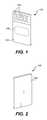
- FIGS. 1 and 2illustrate a memory card according to one embodiment of the invention.
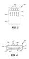
- FIGS. 3 and 4illustrate a memory card according to one embodiment of the invention.
- FIGS. 5 and 6illustrate a memory card according to one embodiment of the invention.
- FIG. 7illustrates a cross-sectional view of a memory card according to one embodiment of the invention.
- FIGS. 8 and 9illustrate a memory card according to another embodiment of the invention.
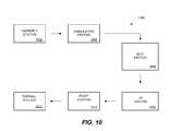
- FIG. 10is a flow diagram of a final assembly process according to one embodiment of the invention.
- FIG. 11is a flow diagram of an electronic device card production process according to one embodiment of the invention.
- FIG. 12is a flow diagram of a memory card production process according to one embodiment of the invention.
- the inventionrelates to improved techniques to produce integrated circuit products.
- the improved techniquespermit smaller and less costly production of integrated circuit products.
- One aspect of the inventionconcerns covering test contacts (e.g., test pins) provided with the integrated circuit products using printed ink. Once covered with the ink, the test contacts are no longer electrically exposed. Hence, the integrated circuit products are not susceptible to accidental access or electrostatic discharge. Moreover, the integrated circuit products can be efficiently produced in a small form factor without any need for additional packaging or labels to electrically isolate the test contacts.
- the integrated circuit productscan be formed using semiconductor assembly techniques.
- the integrated circuit productscan also have a reduced form factor.
- the reduced form factorcan be on the order of chip scale packaging. Further, the form factor can be defined at the semiconductor assembly level of semiconductor manufacturing.
- the integrated circuit productscan pertain to removable peripheral cards.
- the removable peripheral cardscan serve many applications and perform many different functions.
- One type of removable peripheral cardis referred to as a memory card.
- Memory cardsare typically small, integrated circuit-based products that provide data storage. These memory cards plug into or are received by ports or connectors on electronic devices, including computers, cameras, mobile phones and PDAs.
- the memory cardscan be non-volatile memory cards.
- the memory cardscan contain multiple integrated circuit chips stacked on one or both sides of a substrate or leadframe.
- FIGS. 1 and 2illustrate a memory card 100 according to one embodiment of the invention.
- a back side 102 of the memory card 100is primarily depicted.
- a front side 108 of the memory card 100is primarily depicted.
- the memory card 100includes a plurality of input/output (I/O) contacts 104 (e.g., I/O pins) on the back side 102 of the memory card 100 .
- I/O contacts 104are provided towards one end of the memory card 100 .
- the memory card 100has an ink coating 106 .
- the ink coating 106is provided on the back side 102 of the memory card 100 .
- the back side 102 of the memory card 100includes a plurality of test contacts (not shown) that are exposed on the back side 102 of the memory card 100 once assembled. These test contacts are utilized to test the memory card 100 after it has been assembled. After the testing of the memory card 100 has completed, access to the test contacts is no longer normally needed.
- the ink coating 106is provided over the test contacts.
- the ink coating 106provides electrical isolation for the test contacts which would otherwise be exposed.
- the ink coating 106can prevent damage to electrical components or loss of stored data within the memory card 100 due to electrostatic discharge.
- the ink coating 106can prevent unintentional access or damage to stored data within the memory card 100 .
- the ink coating 106can operate to camouflage the test contacts. For example, if the back side 102 of the memory card 100 is black in color, the ink coating 106 could utilize black ink to coat the electrical contacts. As a result, the existence of the test contacts would have been camouflaged or masked so as to be not easily perceptible to end users of the memory card 100 .
- the test contactsare conventionally used to test some degree of internal functionality of the memory card.
- the memory cardincludes a controller integrated circuit (controller chip/die) and a separate memory integrated circuit (memory chip/die) with internal connections between the two chips
- controller chip/diecontroller integrated circuit
- memory chip/diememory integrated circuit
- test pinsit is also possible to use these test pins to preload content to the memory chip and thus make such content available to the end user.
- this processmay be performed faster than using the standard I/O contacts since the interface to the memory chip may be a parallel interface allowing more rapid data transfer than otherwise attainable through a host interface, which might be a slower serial interface.
- the ability to introduce higher voltages or source or sink higher currents than used during normal operationmay be desirable such as when the memory chip is a one-time programmable device where the programming environment may be quite different than the user environment.
- FIGS. 3 and 4illustrate a memory card 300 according to one embodiment of the invention.
- the memory card 300 illustrated in FIGS. 3 and 4is a memory card in which the card has been fully formed (i.e., assembled), except that the test contacts remain exposed.
- the memory card 300includes a back side 302 and a front side 304 .
- the back side 302includes I/O contacts 306 as well as test contacts 308 .
- the test contacts 308can be arranged as a two-dimensional array of test contacts.
- FIG. 4illustrates a cross-sectional view of the memory card 300 .
- the back side 302 of the memory card 300is formed from a back side of a circuit board 310 .
- On the back side 302are provided the I/O contacts 306 and the test contacts 308 .
- the circuit board 310also includes a front side 312 .
- a semiconductor die 314can attached to the front side 312 of the circuit board 310 .
- a plurality of wire bonds 316electrically connect the semiconductor die 314 to bonding pads 318 provided on the front side 312 of the circuit board 310 .
- wire bonds 316are utilized in FIG. 4 , in other embodiments electrical connections can be made by other means (e.g., solder balls).
- the memory card 300 illustrated in FIGS. 3 and 4is assembled but not completely formed.
- the test contacts 308 in the memory card 300 illustrated in FIGS. 3 and 4are exposed so that post-assembly testing can be performed.
- an ink coatingis provided over the test contacts 308 .
- the resulting ink coatingcan be a uniform area that surrounds all of the test contacts 308 .
- the ink coatingcan be concentrated over the individual test contacts 308 .
- the ink coatingcan be formed, for example, by an ink jet printing action. The ink jet printing action operates (via a series of nozzles) to shoot small droplets of ink onto a surface with high precision.
- the nozzlesare part of a print head that can be moved back and forth (e.g., by a stepper motor) with respect to the surface being printed.
- the surface being printedcan also be moved relative to the print head.
- the inkcan be printed with high resolution and with one or more colors.
- the ink jet printing actioncan be induced by various technologies such as known in the art, including piezo or thermal ink jet printers.
- suitable ink jet print headscan be obtains by vendors such as Markem Corporation of Keene, N.H.
- test contacts 308can be arranged as a two-dimensional array of test contacts as illustrated in FIG. 3 , it should be understood that the test contacts can more generally be arranged in a wide range of configurations on any side or surface of a memory card.
- the test contactscan also be provided on more than one side or surface of a memory card.
- the number of test contactscan also vary with implementation (e.g., testing needs or requirements).
- FIGS. 5 and 6illustrate a memory card 500 according to one embodiment of the invention.
- the memory card 500has a back side 502 and a front side 504 .
- the back side 502 of the memory card 500is depicted.
- FIG. 6a cross-sectional view of the memory card 500 is depicted.
- the back side 502 of the memory card 500includes I/O contacts 506 and an ink coating region 508 .
- the ink coating region 508coats all of test contacts 510 with a single, contiguous region of ink.
- the test contacts 510are provided at the back side 502 of a circuit board 512 .
- the I/O contacts 506are also provided at the back side 502 of the circuit board 512 .
- the circuit board 502also includes a front side 514 .
- a semiconductor die 516is attached to the front side 514 of the circuit board 512 .
- a plurality of wire bonds 518can serve to electrically connect the semiconductor die 516 to the circuit board 512 via bonding pads 520 provided at the front surface 514 of the circuit board 512 .
- a molding compound 522can be formed around the semiconductor die 516 and the wire bonds 518 to form the front side 504 of the memory card 500 .
- the edges of the ink coating region 508are rounded.
- a memory cardsuch as the memory card 500
- the presence of the rounded edges for the ink coating 508are advantageous since it is not only results in less frictional resistance to insertion or removal but is also less likely to cause an obstruction or interference as compared to prior art approaches.
- the front side 504 of the memory card 500is a formed molding compound 522 that encompasses the semiconductor die 516 , the wire bonds 518 , and the remaining portion of the front surface 514 of the circuit board 512 .
- the molding compound 522thus forms the front portion (including the front side 504 ) of the memory card 500 .
- the circuit board 512forms the back portion (including the back side 502 ) of the memory card 500 .
- FIG. 7illustrates a cross-sectional view of a memory card 700 according to one embodiment of the invention.
- the memory card 700 illustrated in FIG. 7is generally similar to the memory card 500 illustrated in FIG. 6 .
- the memory card 700further includes a second semiconductor die 524 that is attached to the upper surface of the semiconductor die 516 .
- a layer of adhesive(not shown) can be provided between the semiconductor die 516 and the second semiconductor die 524 .
- the wire bonds 518electrically connect the semiconductor die 516 to die pads 520 provided on the front surface 514 of the circuit board 512 .
- Wire bonds 526electrically connect the semiconductor die 524 to die pads 528 provided on the front surface 514 of the circuit board 512 .
- the semiconductor die 516can pertain to a memory array that provides data storage and the second semiconductor die 524 can provide a controller that controls access to the memory array by way of the I/O contacts 506 .
- FIGS. 8 and 9illustrate a memory card 800 according to another embodiment of the invention.
- the memory card 800has a back side 802 and a front side 804 .
- the back side 802 of the memory card 800is illustrated in FIG. 8 .
- FIG. 9a cross-sectional view of the memory card 800 is illustrated.
- the back side 802 of the memory card 800includes a plurality of I/O contacts 806 .
- the back side 802 of the memory card 800includes a plurality of ink deposits 808 .
- the ink deposits 808are respectively provided over electrical contacts 810 .
- the electrical contacts 810 being provided under the ink deposits 808can be arranged similar to the electrical contacts 308 illustrated in FIG. 3 .
- the back side 802 of the memory card 800is a back side of a circuit board 812 .
- a front side 814 of the circuit board 812has a semiconductor die 816 attached thereto.
- the semiconductor die 816is electrically connected by wire bonds 818 to die pads 820 provided on the front surface 814 of the circuit board 812 .
- the front side 804 of the memory card 800is a formed molding compound 822 that encompasses the semiconductor die 816 , the wire bonds 818 , and the remaining portion of the front surface 814 of the circuit board 812 .
- the molding compound 822thus forms the front portion (including the front side 804 ) of the memory card 800 .
- the circuit board 812forms the back portion (including the back side 802 ) of the memory card 800 .
- the ink deposits 808are deposited on the back side 802 of the memory card 800 over the corresponding test contacts 810 .
- the surface of the back side 802can be substantially smooth, particularly when the test contacts 810 are slightly recessed within the back side 802 of the circuit board 812 .
- the test contactsare formed of a conductive metal, such as gold or copper. In such case, it is advantageous to provide an ink that would adhere to such metal.
- a suitable inkis available from Markem Corporation of Keene, N.H., and can be referred to as a UV cured ink.
- the inkcan include a Cycloaliphatic epoxy resin at 40-60% by weight.
- a less expensive inkcould be utilized if a preparatory coating were provided over the test contacts. The preparatory coating would be designed to adhere to the test contacts and thus permit the ink to in turn adhere to the preparatory coating.
- FIG. 10is a flow diagram of a final assembly process 1000 according to one embodiment of the invention.
- the final assembly process 1000provides an assembly station 1002 .
- a plurality of memory cardscan be assembled in a batch-automated process.
- a circuit board with I/O contacts and test contactscan be provided, one or more semiconductor dies can be placed in contact with a first side of the circuit board, and a molding compound can be formed on at least one side of the circuit board so as to encapsulate the one or more semiconductor dies.
- a second side of the circuit boardcan provide I/O contacts (e.g., I/O pins) and test contacts (e.g., test pins).
- the memory cards being assembledare directed to a singulation station 1004 .
- the memory cardsare singulated into individual memory cards.
- the memory cardsare assembled at the assembly station 1002 as a strip of memory cards.
- the singulation station 1004can operate to cut the strip of memory cards into individual memory cards.
- a test station 1006can be provided to test the individual memory cards.
- the test station 1006can utilize the test contacts that have been formed on the memory cards for the purpose of testing.
- the memory cardsare then directed to a print station 1008 .
- inkis printed onto the back side of the memory cards to cover the test contacts.
- the memory cardsare directed to a ultraviolet (UV) station 1010 .
- UV station 1010the ink that has been dispensed onto the back side of the memory cards is exposed to UV radiation to chemically activate the curing of the ink.
- the inkis UV cured ink.
- the memory cardsare supplied to a thermal station 1012 .
- the memory cardsare heated (or baked) for a predetermined period of time so as to accelerate the curing of the dispensed ink.
- FIG. 11is a flow diagram of an electronic device card production process 1100 according to one embodiment of the invention.
- the electronic device card production process 1100initially provides 1102 a plurality of electronic device cards having exposed test contacts.
- the plurality of electronic device cards being provided 1102can be provided as individual electronic device cards, a strip of adjacent electronic device cards, or an array of electronic device cards.
- the strip or array of electronic devicescan subsequently singulated into individual electronic device cards.
- the electronic device card production process 1100next applies 1104 a coating of ink over the exposed test contacts of the electronic device cards.
- the ink that has been applied 1104 on the electronic device cardscan be cured 1106 .
- the curing processcan vary depending upon the composition of the ink.
- the inkis a UV-cured ink.
- the curing 1106 of the inkcan utilize UV radiation to chemically activate the curing process that can thereafter be followed by a thermal (or baking) process to accelerate the curing process.
- the UV exposurecan be for 4-20 seconds and the baking process can for approximately twenty (20) minutes at about 140° C.
- the electronic device card production process 1100ends, with the electronic device cards being produced in their final form.
- FIG. 12is a flow diagram of a memory card production process 1200 according to one embodiment of the invention.
- the memory card production process 1200is, for example, one implementation of the electronic device card production process 1100 illustrated in FIG. 11 .
- the memory card production process 1200initially fabricates 1202 a strip of memory cards having exposed test contacts. Next, the strip of memory cards is singulated 1204 into individual memory cards. The memory cards are then tested 1206 using the exposed test contacts associated with each of the memory cards. After testing has successfully completed, ink is printed 1208 over the exposed test contacts of the memory cards. Thereafter, the ink printed on the memory cards is cured 1210 . The printed ink can serve to camouflage or mask the test contacts. Additionally, the printed ink can carry text and/or graphics for labeling, marking, marketing, etc.
- the ink being printed 1208 on the memory cardis a UV cured ink.
- the inkis cured 1210 by first applying UV radiation to the ink printed on the memory cards and then applying heat to the ink to accelerate the curing process.
- FIGS. 11 and 12are performed at different times and in different physical locations.
Landscapes
- Engineering & Computer Science (AREA)
- Microelectronics & Electronic Packaging (AREA)
- Power Engineering (AREA)
- Physics & Mathematics (AREA)
- Condensed Matter Physics & Semiconductors (AREA)
- General Physics & Mathematics (AREA)
- Computer Hardware Design (AREA)
- Manufacturing & Machinery (AREA)
- Credit Cards Or The Like (AREA)
Abstract
Description
Claims (26)
Priority Applications (6)
| Application Number | Priority Date | Filing Date | Title |
|---|---|---|---|
| US11/551,423US8013332B2 (en) | 2006-10-20 | 2006-10-20 | Portable memory devices |
| TW096139339ATWI407860B (en) | 2006-10-20 | 2007-10-19 | Portable memory devices and method therefor |
| KR1020097010131AKR101121422B1 (en) | 2006-10-20 | 2007-10-19 | Portable memory devices and method therefor |
| CN2007800390316ACN101542507B (en) | 2006-10-20 | 2007-10-19 | Portable memory device and method thereof |
| PCT/US2007/081924WO2008051838A2 (en) | 2006-10-20 | 2007-10-19 | Portable memory devices and method therefor |
| US13/225,263US20110315987A1 (en) | 2006-10-20 | 2011-09-02 | Portable memory devices |
Applications Claiming Priority (1)
| Application Number | Priority Date | Filing Date | Title |
|---|---|---|---|
| US11/551,423US8013332B2 (en) | 2006-10-20 | 2006-10-20 | Portable memory devices |
Related Child Applications (1)
| Application Number | Title | Priority Date | Filing Date |
|---|---|---|---|
| US13/225,263DivisionUS20110315987A1 (en) | 2006-10-20 | 2011-09-02 | Portable memory devices |
Publications (2)
| Publication Number | Publication Date |
|---|---|
| US20080185582A1 US20080185582A1 (en) | 2008-08-07 |
| US8013332B2true US8013332B2 (en) | 2011-09-06 |
Family
ID=39675377
Family Applications (2)
| Application Number | Title | Priority Date | Filing Date |
|---|---|---|---|
| US11/551,423Active2028-05-26US8013332B2 (en) | 2006-10-20 | 2006-10-20 | Portable memory devices |
| US13/225,263AbandonedUS20110315987A1 (en) | 2006-10-20 | 2011-09-02 | Portable memory devices |
Family Applications After (1)
| Application Number | Title | Priority Date | Filing Date |
|---|---|---|---|
| US13/225,263AbandonedUS20110315987A1 (en) | 2006-10-20 | 2011-09-02 | Portable memory devices |
Country Status (2)
| Country | Link |
|---|---|
| US (2) | US8013332B2 (en) |
| CN (1) | CN101542507B (en) |
Cited By (4)
| Publication number | Priority date | Publication date | Assignee | Title |
|---|---|---|---|---|
| US20110062242A1 (en)* | 2008-03-31 | 2011-03-17 | The Royal Bank Of Scotland Plc | Processor card arrangement |
| US20120313656A1 (en)* | 2009-10-26 | 2012-12-13 | Samsung Sdi Co., Ltd. | Electronic circuit module and method of making the same |
| US8917107B2 (en) | 2007-12-12 | 2014-12-23 | Samsung Electronics Co., Ltd. | Circuit board having bypass pad |
| US20150294737A1 (en)* | 2011-04-21 | 2015-10-15 | Micron Technology, Inc. | Method and apparatus for providing preloaded non-volatile memory content |
Families Citing this family (3)
| Publication number | Priority date | Publication date | Assignee | Title |
|---|---|---|---|---|
| US8690283B2 (en)* | 2009-10-20 | 2014-04-08 | Sandisk Il Ltd. | Method and system for printing graphical content onto a plurality of memory devices and for providing a visually distinguishable memory device |
| US10079156B2 (en) | 2014-11-07 | 2018-09-18 | Advanced Semiconductor Engineering, Inc. | Semiconductor package including dielectric layers defining via holes extending to component pads |
| US9721799B2 (en)* | 2014-11-07 | 2017-08-01 | Advanced Semiconductor Engineering, Inc. | Semiconductor package with reduced via hole width and reduced pad patch and manufacturing method thereof |
Citations (40)
| Publication number | Priority date | Publication date | Assignee | Title |
|---|---|---|---|---|
| US3373409A (en) | 1965-04-20 | 1968-03-12 | Ibm | Information storage unit and memory card therefor |
| US4713298A (en) | 1985-03-15 | 1987-12-15 | M&T Chemicals Inc. | Printed circuit boards having improved adhesion between solder mask and metal |
| EP0581284A2 (en) | 1992-07-30 | 1994-02-02 | Mitsubishi Denki Kabushiki Kaisha | Non-contact IC card and manufacturing and testing methods of the same |
| US5490891A (en) | 1993-07-15 | 1996-02-13 | Duel Systems | Method of manufacturing a memory card package |
| US5502289A (en) | 1992-05-22 | 1996-03-26 | National Semiconductor Corporation | Stacked multi-chip modules and method of manufacturing |
| US5512712A (en) | 1993-10-14 | 1996-04-30 | Ibiden Co., Ltd. | Printed wiring board having indications thereon covered by insulation |
| US5596225A (en) | 1994-10-27 | 1997-01-21 | National Semiconductor Corporation | Leadframe for an integrated circuit package which electrically interconnects multiple integrated circuit die |
| US5663901A (en) | 1991-04-11 | 1997-09-02 | Sandisk Corporation | Computer memory cards using flash EEPROM integrated circuit chips and memory-controller systems |
| US5877544A (en) | 1995-08-23 | 1999-03-02 | Schlumberger Industries | Electronic micropackage for an electronic memory card |
| US5933328A (en) | 1998-07-28 | 1999-08-03 | Sandisk Corporation | Compact mechanism for removable insertion of multiple integrated circuit cards into portable and other electronic devices |
| US6085412A (en) | 1996-06-11 | 2000-07-11 | Kabushiki Kaisha Toshiba | Method for manufacturing card type memory device |
| US6151248A (en) | 1999-06-30 | 2000-11-21 | Sandisk Corporation | Dual floating gate EEPROM cell array with steering gates shared by adjacent cells |
| US6235555B1 (en) | 1998-01-09 | 2001-05-22 | Samsung Electronics Co., Ltd. | Reel-deployed printed circuit board and method for manufacturing chip-on-board packages |
| US6323064B1 (en) | 1999-10-11 | 2001-11-27 | Samsung Electronics Co., Ltd | Method for fabricating a memory card |
| US6333517B1 (en) | 1999-01-12 | 2001-12-25 | Nec Corporation | Semiconductor integrated circuit device equipped with power make-up circuit used in burn-in test after packaging and method for testing the same |
| US6368899B1 (en) | 2000-03-08 | 2002-04-09 | Maxwell Electronic Components Group, Inc. | Electronic device packaging |
| US6372539B1 (en) | 2000-03-20 | 2002-04-16 | National Semiconductor Corporation | Leadless packaging process using a conductive substrate |
| US6399415B1 (en) | 2000-03-20 | 2002-06-04 | National Semiconductor Corporation | Electrical isolation in panels of leadless IC packages |
| US6410355B1 (en) | 1998-06-11 | 2002-06-25 | Sandisk Corporation | Semiconductor package using terminals formed on a conductive layer of a circuit board |
| US6444501B1 (en) | 2001-06-12 | 2002-09-03 | Micron Technology, Inc. | Two stage transfer molding method to encapsulate MMC module |
| WO2002069251A1 (en) | 2001-02-28 | 2002-09-06 | Hitachi, Ltd | Memory card and its manufacturing method |
| US20020131251A1 (en) | 2001-03-16 | 2002-09-19 | Corisis David J. | Semiconductor card and method of fabrication |
| US6456528B1 (en) | 2001-09-17 | 2002-09-24 | Sandisk Corporation | Selective operation of a multi-state non-volatile memory system in a binary mode |
| US6489218B1 (en) | 2001-06-21 | 2002-12-03 | Advanced Semiconductor Engineering, Inc. | Singulation method used in leadless packaging process |
| US6537842B2 (en) | 2000-06-08 | 2003-03-25 | Micron Technology, Inc. | Methods for fabricating protective structures for bond wires |
| US6624005B1 (en) | 2000-09-06 | 2003-09-23 | Amkor Technology, Inc. | Semiconductor memory cards and method of making same |
| US6677183B2 (en) | 2001-01-31 | 2004-01-13 | Canon Kabushiki Kaisha | Method of separation of semiconductor device |
| US20040018667A1 (en) | 2002-07-26 | 2004-01-29 | Haren Joshi | Method and apparatus for producing a silicon wafer chip package |
| US6705925B1 (en) | 2000-10-20 | 2004-03-16 | Lightwave Microsystems | Apparatus and method to dice integrated circuits from a wafer using a pressurized jet |
| US20040058478A1 (en) | 2002-09-25 | 2004-03-25 | Shafidul Islam | Taped lead frames and methods of making and using the same in semiconductor packaging |
| US20040229401A1 (en) | 2003-05-12 | 2004-11-18 | Bolken Todd O. | Method for fabricating semiconductor component having stacked, encapsulated dice |
| US20040259291A1 (en) | 2003-06-23 | 2004-12-23 | Sandisk Corporation | Method for efficiently producing removable peripheral cards |
| US20050013106A1 (en)* | 2003-07-17 | 2005-01-20 | Takiar Hem P. | Peripheral card with hidden test pins |
| US20050200676A1 (en)* | 2004-03-04 | 2005-09-15 | Fuji Photo Film Co., Ltd. | Inkjet recording head and inkjet recording apparatus |
| WO2005091811A2 (en) | 2004-03-03 | 2005-10-06 | Markem Corporation | Jettable ink |
| US20060020469A1 (en) | 2004-07-08 | 2006-01-26 | Rast Rodger H | Apparatus and methods for static and semi-static displays |
| EP1624001A1 (en) | 2003-05-09 | 2006-02-08 | Taiyo Ink Manufacturing Co. Ltd | Photocuring/thermosetting inkjet composition and printed wiring board using same |
| US7051142B2 (en) | 2000-03-08 | 2006-05-23 | Kabushiki Kaisha Toshiba | Electronic device with card interface |
| US7293716B1 (en)* | 2005-02-17 | 2007-11-13 | Amkor Technology, Inc. | Secure digital memory card using land grid array structure |
| US7402897B2 (en) | 2002-08-08 | 2008-07-22 | Elm Technology Corporation | Vertical system integration |
Family Cites Families (1)
| Publication number | Priority date | Publication date | Assignee | Title |
|---|---|---|---|---|
| PT103018A (en)* | 2003-09-12 | 2005-03-31 | Univ Do Minho | PROCESS FOR OBTAINING FISH IN G-TIAI BY FOUNDATION |
- 2006
- 2006-10-20USUS11/551,423patent/US8013332B2/enactiveActive
- 2007
- 2007-10-19CNCN2007800390316Apatent/CN101542507B/ennot_activeExpired - Fee Related
- 2011
- 2011-09-02USUS13/225,263patent/US20110315987A1/ennot_activeAbandoned
Patent Citations (43)
| Publication number | Priority date | Publication date | Assignee | Title |
|---|---|---|---|---|
| US3373409A (en) | 1965-04-20 | 1968-03-12 | Ibm | Information storage unit and memory card therefor |
| US4713298A (en) | 1985-03-15 | 1987-12-15 | M&T Chemicals Inc. | Printed circuit boards having improved adhesion between solder mask and metal |
| US5663901A (en) | 1991-04-11 | 1997-09-02 | Sandisk Corporation | Computer memory cards using flash EEPROM integrated circuit chips and memory-controller systems |
| US5502289A (en) | 1992-05-22 | 1996-03-26 | National Semiconductor Corporation | Stacked multi-chip modules and method of manufacturing |
| EP0581284A2 (en) | 1992-07-30 | 1994-02-02 | Mitsubishi Denki Kabushiki Kaisha | Non-contact IC card and manufacturing and testing methods of the same |
| US5490891A (en) | 1993-07-15 | 1996-02-13 | Duel Systems | Method of manufacturing a memory card package |
| US5512712A (en) | 1993-10-14 | 1996-04-30 | Ibiden Co., Ltd. | Printed wiring board having indications thereon covered by insulation |
| US5596225A (en) | 1994-10-27 | 1997-01-21 | National Semiconductor Corporation | Leadframe for an integrated circuit package which electrically interconnects multiple integrated circuit die |
| US5877544A (en) | 1995-08-23 | 1999-03-02 | Schlumberger Industries | Electronic micropackage for an electronic memory card |
| US6085412A (en) | 1996-06-11 | 2000-07-11 | Kabushiki Kaisha Toshiba | Method for manufacturing card type memory device |
| US6235555B1 (en) | 1998-01-09 | 2001-05-22 | Samsung Electronics Co., Ltd. | Reel-deployed printed circuit board and method for manufacturing chip-on-board packages |
| US6410355B1 (en) | 1998-06-11 | 2002-06-25 | Sandisk Corporation | Semiconductor package using terminals formed on a conductive layer of a circuit board |
| US5933328A (en) | 1998-07-28 | 1999-08-03 | Sandisk Corporation | Compact mechanism for removable insertion of multiple integrated circuit cards into portable and other electronic devices |
| US6333517B1 (en) | 1999-01-12 | 2001-12-25 | Nec Corporation | Semiconductor integrated circuit device equipped with power make-up circuit used in burn-in test after packaging and method for testing the same |
| US6151248A (en) | 1999-06-30 | 2000-11-21 | Sandisk Corporation | Dual floating gate EEPROM cell array with steering gates shared by adjacent cells |
| US6323064B1 (en) | 1999-10-11 | 2001-11-27 | Samsung Electronics Co., Ltd | Method for fabricating a memory card |
| US6368899B1 (en) | 2000-03-08 | 2002-04-09 | Maxwell Electronic Components Group, Inc. | Electronic device packaging |
| US7051142B2 (en) | 2000-03-08 | 2006-05-23 | Kabushiki Kaisha Toshiba | Electronic device with card interface |
| US6372539B1 (en) | 2000-03-20 | 2002-04-16 | National Semiconductor Corporation | Leadless packaging process using a conductive substrate |
| US6399415B1 (en) | 2000-03-20 | 2002-06-04 | National Semiconductor Corporation | Electrical isolation in panels of leadless IC packages |
| US6537842B2 (en) | 2000-06-08 | 2003-03-25 | Micron Technology, Inc. | Methods for fabricating protective structures for bond wires |
| US6624005B1 (en) | 2000-09-06 | 2003-09-23 | Amkor Technology, Inc. | Semiconductor memory cards and method of making same |
| US6705925B1 (en) | 2000-10-20 | 2004-03-16 | Lightwave Microsystems | Apparatus and method to dice integrated circuits from a wafer using a pressurized jet |
| US6677183B2 (en) | 2001-01-31 | 2004-01-13 | Canon Kabushiki Kaisha | Method of separation of semiconductor device |
| WO2002069251A1 (en) | 2001-02-28 | 2002-09-06 | Hitachi, Ltd | Memory card and its manufacturing method |
| US20040090829A1 (en) | 2001-02-28 | 2004-05-13 | Tomomi Miura | Memory card and its manufacturing method |
| US20020131251A1 (en) | 2001-03-16 | 2002-09-19 | Corisis David J. | Semiconductor card and method of fabrication |
| US6444501B1 (en) | 2001-06-12 | 2002-09-03 | Micron Technology, Inc. | Two stage transfer molding method to encapsulate MMC module |
| US6489218B1 (en) | 2001-06-21 | 2002-12-03 | Advanced Semiconductor Engineering, Inc. | Singulation method used in leadless packaging process |
| US6456528B1 (en) | 2001-09-17 | 2002-09-24 | Sandisk Corporation | Selective operation of a multi-state non-volatile memory system in a binary mode |
| US20040018667A1 (en) | 2002-07-26 | 2004-01-29 | Haren Joshi | Method and apparatus for producing a silicon wafer chip package |
| US7402897B2 (en) | 2002-08-08 | 2008-07-22 | Elm Technology Corporation | Vertical system integration |
| US20040058478A1 (en) | 2002-09-25 | 2004-03-25 | Shafidul Islam | Taped lead frames and methods of making and using the same in semiconductor packaging |
| EP1624001A1 (en) | 2003-05-09 | 2006-02-08 | Taiyo Ink Manufacturing Co. Ltd | Photocuring/thermosetting inkjet composition and printed wiring board using same |
| US20040229401A1 (en) | 2003-05-12 | 2004-11-18 | Bolken Todd O. | Method for fabricating semiconductor component having stacked, encapsulated dice |
| US20040259291A1 (en) | 2003-06-23 | 2004-12-23 | Sandisk Corporation | Method for efficiently producing removable peripheral cards |
| US7094633B2 (en) | 2003-06-23 | 2006-08-22 | Sandisk Corporation | Method for efficiently producing removable peripheral cards |
| US20060267165A1 (en) | 2003-06-23 | 2006-11-30 | Sandisk Corporation | Method for efficiently producing removable peripheral cards |
| US20050013106A1 (en)* | 2003-07-17 | 2005-01-20 | Takiar Hem P. | Peripheral card with hidden test pins |
| WO2005091811A2 (en) | 2004-03-03 | 2005-10-06 | Markem Corporation | Jettable ink |
| US20050200676A1 (en)* | 2004-03-04 | 2005-09-15 | Fuji Photo Film Co., Ltd. | Inkjet recording head and inkjet recording apparatus |
| US20060020469A1 (en) | 2004-07-08 | 2006-01-26 | Rast Rodger H | Apparatus and methods for static and semi-static displays |
| US7293716B1 (en)* | 2005-02-17 | 2007-11-13 | Amkor Technology, Inc. | Secure digital memory card using land grid array structure |
Non-Patent Citations (18)
| Title |
|---|
| "4000 DOD Ink Jet Printer", Markem Corporation, Keene, NH., 2006, pp. 1-2. |
| "4601", Markem Corporation, Keene, NH., 2006, pp. 1-2. |
| "UV Cure Jetting Ink", Markem Corporation, Keene, NH., 2006, pp. 1-2. |
| Dean et al., "New Fine-Beam, Abrasive Water Jet Technology Enables Photonic and Small Device Singulation," Chip Scale Review, Aug./Sep. 2002, pp. 43, 45, 47. |
| High Capacity and Small Size, Meeting the Storage Needs to Today's Portable Devices, 2003 SanDisk Corporation. |
| International Search Report and Written Opinion for PCT/US2007/081924, mailed on Apr. 18, 2008. |
| Notice of Allowance dated Dec. 14, 2010 in U.S. Appl. No. 11/551,402. |
| Office Action dated Dec. 13, 2010 in Korean Patent Application No. 2009-7010131. |
| Office Action dated Feb. 21, 2008 for U.S. Appl. No. 11/551,402. |
| Office Action dated Jun. 14, 2011 in Chinese Patent Application No. 200780039031.6. |
| Office Action dated Jun. 25, 2009 for U.S. Appl. No. 11/551,402. |
| Office Action dated Mar. 25, 2010, U.S. Appl. No. 11/551,402. |
| Office Action dated Oct. 10, 2008 for U.S. Appl. No. 11/551,402. |
| Office Action dated Sep. 28, 2010 in Taiwanese Patent Application No. 096139339. |
| Response to Office Action dated Sep. 27, 2010 in U.S. Appl. No. 11/551,402, filed Oct. 20, 2006. |
| Response to Office Action filed Mar. 29, 2011 in Taiwanese Patent Application No. 096139339. |
| The MultiMedia Card System Summary, Version 3.2, MMCA Technical Committee, Jan. 2002. |
| U.S. Appl. No. 11/551,402, entitled "Method for Producing Portable Memory Devices", filed Oct. 20, 2006. |
Cited By (11)
| Publication number | Priority date | Publication date | Assignee | Title |
|---|---|---|---|---|
| US8917107B2 (en) | 2007-12-12 | 2014-12-23 | Samsung Electronics Co., Ltd. | Circuit board having bypass pad |
| US9069036B2 (en) | 2007-12-12 | 2015-06-30 | Samsung Electronics Co., Ltd. | Circuit board having bypass pad |
| US9171644B2 (en) | 2007-12-12 | 2015-10-27 | Samsung Electronics Co., Ltd. | Circuit board having bypass pad |
| US9449716B2 (en) | 2007-12-12 | 2016-09-20 | Samsung Electronics Co., Ltd. | Circuit board having bypass pad |
| US9627360B2 (en) | 2007-12-12 | 2017-04-18 | Samsung Electronics Co., Ltd. | Circuit board having bypass pad |
| US20110062242A1 (en)* | 2008-03-31 | 2011-03-17 | The Royal Bank Of Scotland Plc | Processor card arrangement |
| US8550362B2 (en)* | 2008-03-31 | 2013-10-08 | The Royal Bank Of Scotland Plc | Processor card arrangement |
| US20120313656A1 (en)* | 2009-10-26 | 2012-12-13 | Samsung Sdi Co., Ltd. | Electronic circuit module and method of making the same |
| US8773865B2 (en)* | 2009-10-26 | 2014-07-08 | Samsung Sdi Co., Ltd. | Electronic circuit module and method of making the same |
| US20150294737A1 (en)* | 2011-04-21 | 2015-10-15 | Micron Technology, Inc. | Method and apparatus for providing preloaded non-volatile memory content |
| US10242751B2 (en)* | 2011-04-21 | 2019-03-26 | Micron Technology, Inc. | Method and apparatus for providing preloaded non-volatile memory content |
Also Published As
| Publication number | Publication date |
|---|---|
| CN101542507A (en) | 2009-09-23 |
| CN101542507B (en) | 2012-12-26 |
| US20110315987A1 (en) | 2011-12-29 |
| US20080185582A1 (en) | 2008-08-07 |
Similar Documents
| Publication | Publication Date | Title |
|---|---|---|
| US7928010B2 (en) | Method for producing portable memory devices | |
| US20110315987A1 (en) | Portable memory devices | |
| US7307848B2 (en) | Memory card with raised portion | |
| US7864540B2 (en) | Peripheral card with sloped edges | |
| US8254134B2 (en) | Molded memory card with write protection switch assembly | |
| US7094633B2 (en) | Method for efficiently producing removable peripheral cards | |
| US7872871B2 (en) | Molding methods to manufacture single-chip chip-on-board USB device | |
| US7466556B2 (en) | Single chip USB packages with swivel cover | |
| US20080286990A1 (en) | Direct Package Mold Process For Single Chip SD Flash Cards | |
| US20050011671A1 (en) | Memory card with and without enclosure | |
| US20080020641A1 (en) | Single Chip USB Packages By Various Assembly Methods | |
| US20080195817A1 (en) | SD Flash Memory Card Manufacturing Using Rigid-Flex PCB | |
| CN109643697A (en) | Method of manufacturing flexible electronic circuits with conformal material coatings | |
| US8283664B2 (en) | Disguising test pads in a semiconductor package | |
| KR101121422B1 (en) | Portable memory devices and method therefor | |
| TW484102B (en) | Method for producing a plastic object containing an electrically conducting structure |
Legal Events
| Date | Code | Title | Description |
|---|---|---|---|
| AS | Assignment | Owner name:SANDISK CORPORATION, CALIFORNIA Free format text:ASSIGNMENT OF ASSIGNORS INTEREST;ASSIGNORS:MIDDLEKAUFF, WARREN;MILLER, ROBERT;REEL/FRAME:019058/0047 Effective date:20070301 | |
| AS | Assignment | Owner name:SANDISK CORPORATION, CALIFORNIA Free format text:ASSIGNMENT OF ASSIGNORS INTEREST;ASSIGNOR:CENTOFANTE, CHARLIE;REEL/FRAME:020804/0320 Effective date:20080408 | |
| AS | Assignment | Owner name:SANDISK TECHNOLOGIES INC., TEXAS Free format text:ASSIGNMENT OF ASSIGNORS INTEREST;ASSIGNOR:SANDISK CORPORATION;REEL/FRAME:026227/0072 Effective date:20110404 | |
| STCF | Information on status: patent grant | Free format text:PATENTED CASE | |
| FPAY | Fee payment | Year of fee payment:4 | |
| AS | Assignment | Owner name:SANDISK TECHNOLOGIES LLC, TEXAS Free format text:CHANGE OF NAME;ASSIGNOR:SANDISK TECHNOLOGIES INC;REEL/FRAME:038809/0472 Effective date:20160516 | |
| MAFP | Maintenance fee payment | Free format text:PAYMENT OF MAINTENANCE FEE, 8TH YEAR, LARGE ENTITY (ORIGINAL EVENT CODE: M1552); ENTITY STATUS OF PATENT OWNER: LARGE ENTITY Year of fee payment:8 | |
| FEPP | Fee payment procedure | Free format text:MAINTENANCE FEE REMINDER MAILED (ORIGINAL EVENT CODE: REM.); ENTITY STATUS OF PATENT OWNER: LARGE ENTITY | |
| FEPP | Fee payment procedure | Free format text:11.5 YR SURCHARGE- LATE PMT W/IN 6 MO, LARGE ENTITY (ORIGINAL EVENT CODE: M1556); ENTITY STATUS OF PATENT OWNER: LARGE ENTITY | |
| MAFP | Maintenance fee payment | Free format text:PAYMENT OF MAINTENANCE FEE, 12TH YEAR, LARGE ENTITY (ORIGINAL EVENT CODE: M1553); ENTITY STATUS OF PATENT OWNER: LARGE ENTITY Year of fee payment:12 | |
| AS | Assignment | Owner name:SANDISK TECHNOLOGIES, INC., CALIFORNIA Free format text:ASSIGNMENT OF ASSIGNORS INTEREST;ASSIGNOR:SANDISK TECHNOLOGIES LLC;REEL/FRAME:069796/0423 Effective date:20241227 | |
| AS | Assignment | Owner name:SANDISK TECHNOLOGIES, INC., CALIFORNIA Free format text:PARTIAL RELEASE OF SECURITY INTERESTS;ASSIGNOR:JPMORGAN CHASE BANK, N.A., AS AGENT;REEL/FRAME:071382/0001 Effective date:20250424 Owner name:JPMORGAN CHASE BANK, N.A., AS COLLATERAL AGENT, ILLINOIS Free format text:SECURITY AGREEMENT;ASSIGNOR:SANDISK TECHNOLOGIES, INC.;REEL/FRAME:071050/0001 Effective date:20250424 |