US8012395B2 - Template having alignment marks formed of contrast material - Google Patents
Template having alignment marks formed of contrast materialDownload PDFInfo
- Publication number
- US8012395B2 US8012395B2US12/464,487US46448709AUS8012395B2US 8012395 B2US8012395 B2US 8012395B2US 46448709 AUS46448709 AUS 46448709AUS 8012395 B2US8012395 B2US 8012395B2
- Authority
- US
- United States
- Prior art keywords
- substrate
- patterning
- alignment marks
- contrast material
- template
- Prior art date
- Legal status (The legal status is an assumption and is not a legal conclusion. Google has not performed a legal analysis and makes no representation as to the accuracy of the status listed.)
- Active, expires
Links
- 239000002872contrast mediaSubstances0.000titleclaimsabstractdescription57
- 239000000758substrateSubstances0.000claimsabstractdescription110
- 238000000034methodMethods0.000claimsabstractdescription64
- 239000010410layerSubstances0.000claimsdescription93
- 238000000059patterningMethods0.000claimsdescription33
- 230000015572biosynthetic processEffects0.000claimsdescription18
- 239000011241protective layerSubstances0.000claimsdescription9
- 238000005530etchingMethods0.000claimsdescription6
- 238000000151depositionMethods0.000claimsdescription3
- 238000005329nanolithographyMethods0.000claims2
- 238000001459lithographyMethods0.000abstractdescription6
- 239000000463materialSubstances0.000description31
- 238000005755formation reactionMethods0.000description17
- 238000012545processingMethods0.000description10
- 238000004519manufacturing processMethods0.000description8
- VYZAMTAEIAYCRO-UHFFFAOYSA-NChromiumChemical compound[Cr]VYZAMTAEIAYCRO-UHFFFAOYSA-N0.000description6
- 229910052804chromiumInorganic materials0.000description6
- 239000011651chromiumSubstances0.000description6
- ZOKXTWBITQBERF-UHFFFAOYSA-NMolybdenumChemical compound[Mo]ZOKXTWBITQBERF-UHFFFAOYSA-N0.000description3
- VYPSYNLAJGMNEJ-UHFFFAOYSA-NSilicium dioxideChemical compoundO=[Si]=OVYPSYNLAJGMNEJ-UHFFFAOYSA-N0.000description3
- RTAQQCXQSZGOHL-UHFFFAOYSA-NTitaniumChemical compound[Ti]RTAQQCXQSZGOHL-UHFFFAOYSA-N0.000description3
- NRTOMJZYCJJWKI-UHFFFAOYSA-NTitanium nitrideChemical compound[Ti]#NNRTOMJZYCJJWKI-UHFFFAOYSA-N0.000description3
- 229910021417amorphous siliconInorganic materials0.000description3
- SJKRCWUQJZIWQB-UHFFFAOYSA-Nazane;chromiumChemical compoundN.[Cr]SJKRCWUQJZIWQB-UHFFFAOYSA-N0.000description3
- YXTPWUNVHCYOSP-UHFFFAOYSA-Nbis($l^{2}-silanylidene)molybdenumChemical compound[Si]=[Mo]=[Si]YXTPWUNVHCYOSP-UHFFFAOYSA-N0.000description3
- 239000012530fluidSubstances0.000description3
- 239000007788liquidSubstances0.000description3
- 230000033001locomotionEffects0.000description3
- 229910052750molybdenumInorganic materials0.000description3
- 239000011733molybdenumSubstances0.000description3
- 229910021344molybdenum silicideInorganic materials0.000description3
- HBMJWWWQQXIZIP-UHFFFAOYSA-Nsilicon carbideChemical compound[Si+]#[C-]HBMJWWWQQXIZIP-UHFFFAOYSA-N0.000description3
- 229910010271silicon carbideInorganic materials0.000description3
- 229910052715tantalumInorganic materials0.000description3
- GUVRBAGPIYLISA-UHFFFAOYSA-Ntantalum atomChemical compound[Ta]GUVRBAGPIYLISA-UHFFFAOYSA-N0.000description3
- MZLGASXMSKOWSE-UHFFFAOYSA-Ntantalum nitrideChemical compound[Ta]#NMZLGASXMSKOWSE-UHFFFAOYSA-N0.000description3
- 229910052719titaniumInorganic materials0.000description3
- 239000010936titaniumSubstances0.000description3
- WFKWXMTUELFFGS-UHFFFAOYSA-NtungstenChemical compound[W]WFKWXMTUELFFGS-UHFFFAOYSA-N0.000description3
- 229910052721tungstenInorganic materials0.000description3
- 239000010937tungstenSubstances0.000description3
- 238000001039wet etchingMethods0.000description3
- 239000005388borosilicate glassSubstances0.000description2
- -1but not limited toSubstances0.000description2
- 238000005229chemical vapour depositionMethods0.000description2
- 238000004132cross linkingMethods0.000description2
- 238000013461designMethods0.000description2
- KPUWHANPEXNPJT-UHFFFAOYSA-NdisiloxaneChemical class[SiH3]O[SiH3]KPUWHANPEXNPJT-UHFFFAOYSA-N0.000description2
- 238000010894electron beam technologyMethods0.000description2
- 239000010408filmSubstances0.000description2
- 229920002313fluoropolymerPolymers0.000description2
- 238000002955isolationMethods0.000description2
- 229910052751metalInorganic materials0.000description2
- 239000002184metalSubstances0.000description2
- 230000003287optical effectEffects0.000description2
- 229920000620organic polymerPolymers0.000description2
- 238000005240physical vapour depositionMethods0.000description2
- 238000001020plasma etchingMethods0.000description2
- 229920000642polymerPolymers0.000description2
- 238000006116polymerization reactionMethods0.000description2
- 239000010453quartzSubstances0.000description2
- 230000010076replicationEffects0.000description2
- 229910052594sapphireInorganic materials0.000description2
- 239000010980sapphireSubstances0.000description2
- 229910052710siliconInorganic materials0.000description2
- 239000010703siliconSubstances0.000description2
- 238000004528spin coatingMethods0.000description2
- 238000012546transferMethods0.000description2
- ZAMOUSCENKQFHK-UHFFFAOYSA-NChlorine atomChemical compound[Cl]ZAMOUSCENKQFHK-UHFFFAOYSA-N0.000description1
- QVGXLLKOCUKJST-UHFFFAOYSA-Natomic oxygenChemical compound[O]QVGXLLKOCUKJST-UHFFFAOYSA-N0.000description1
- 239000000460chlorineSubstances0.000description1
- 229910052801chlorineInorganic materials0.000description1
- 238000004891communicationMethods0.000description1
- 230000008021depositionEffects0.000description1
- 238000011161developmentMethods0.000description1
- 238000003618dip coatingMethods0.000description1
- 230000009977dual effectEffects0.000description1
- 230000000694effectsEffects0.000description1
- 238000000609electron-beam lithographyMethods0.000description1
- 238000005516engineering processMethods0.000description1
- 238000013467fragmentationMethods0.000description1
- 238000006062fragmentation reactionMethods0.000description1
- 239000005350fused silica glassSubstances0.000description1
- 239000007789gasSubstances0.000description1
- 239000000203mixtureSubstances0.000description1
- 239000000178monomerSubstances0.000description1
- NJPPVKZQTLUDBO-UHFFFAOYSA-NnovaluronChemical compoundC1=C(Cl)C(OC(F)(F)C(OC(F)(F)F)F)=CC=C1NC(=O)NC(=O)C1=C(F)C=CC=C1FNJPPVKZQTLUDBO-UHFFFAOYSA-N0.000description1
- 239000001301oxygenSubstances0.000description1
- 229910052760oxygenInorganic materials0.000description1
- 238000004886process controlMethods0.000description1
- 230000005855radiationEffects0.000description1
- 230000001105regulatory effectEffects0.000description1
- 239000004065semiconductorSubstances0.000description1
- 238000007711solidificationMethods0.000description1
- 230000008023solidificationEffects0.000description1
- 239000002904solventSubstances0.000description1
- 238000003892spreadingMethods0.000description1
- 238000000427thin-film depositionMethods0.000description1
- XLYOFNOQVPJJNP-UHFFFAOYSA-NwaterSubstancesOXLYOFNOQVPJJNP-UHFFFAOYSA-N0.000description1
- 229910052724xenonInorganic materials0.000description1
- FHNFHKCVQCLJFQ-UHFFFAOYSA-Nxenon atomChemical compound[Xe]FHNFHKCVQCLJFQ-UHFFFAOYSA-N0.000description1
Images


Classifications
- G—PHYSICS
- G03—PHOTOGRAPHY; CINEMATOGRAPHY; ANALOGOUS TECHNIQUES USING WAVES OTHER THAN OPTICAL WAVES; ELECTROGRAPHY; HOLOGRAPHY
- G03F—PHOTOMECHANICAL PRODUCTION OF TEXTURED OR PATTERNED SURFACES, e.g. FOR PRINTING, FOR PROCESSING OF SEMICONDUCTOR DEVICES; MATERIALS THEREFOR; ORIGINALS THEREFOR; APPARATUS SPECIALLY ADAPTED THEREFOR
- G03F9/00—Registration or positioning of originals, masks, frames, photographic sheets or textured or patterned surfaces, e.g. automatically
- G03F9/70—Registration or positioning of originals, masks, frames, photographic sheets or textured or patterned surfaces, e.g. automatically for microlithography
- G03F9/7003—Alignment type or strategy, e.g. leveling, global alignment
- G03F9/7042—Alignment for lithographic apparatus using patterning methods other than those involving the exposure to radiation, e.g. by stamping or imprinting
- B—PERFORMING OPERATIONS; TRANSPORTING
- B82—NANOTECHNOLOGY
- B82Y—SPECIFIC USES OR APPLICATIONS OF NANOSTRUCTURES; MEASUREMENT OR ANALYSIS OF NANOSTRUCTURES; MANUFACTURE OR TREATMENT OF NANOSTRUCTURES
- B82Y10/00—Nanotechnology for information processing, storage or transmission, e.g. quantum computing or single electron logic
- B—PERFORMING OPERATIONS; TRANSPORTING
- B82—NANOTECHNOLOGY
- B82Y—SPECIFIC USES OR APPLICATIONS OF NANOSTRUCTURES; MEASUREMENT OR ANALYSIS OF NANOSTRUCTURES; MANUFACTURE OR TREATMENT OF NANOSTRUCTURES
- B82Y40/00—Manufacture or treatment of nanostructures
- G—PHYSICS
- G03—PHOTOGRAPHY; CINEMATOGRAPHY; ANALOGOUS TECHNIQUES USING WAVES OTHER THAN OPTICAL WAVES; ELECTROGRAPHY; HOLOGRAPHY
- G03F—PHOTOMECHANICAL PRODUCTION OF TEXTURED OR PATTERNED SURFACES, e.g. FOR PRINTING, FOR PROCESSING OF SEMICONDUCTOR DEVICES; MATERIALS THEREFOR; ORIGINALS THEREFOR; APPARATUS SPECIALLY ADAPTED THEREFOR
- G03F7/00—Photomechanical, e.g. photolithographic, production of textured or patterned surfaces, e.g. printing surfaces; Materials therefor, e.g. comprising photoresists; Apparatus specially adapted therefor
- G03F7/0002—Lithographic processes using patterning methods other than those involving the exposure to radiation, e.g. by stamping
- G—PHYSICS
- G03—PHOTOGRAPHY; CINEMATOGRAPHY; ANALOGOUS TECHNIQUES USING WAVES OTHER THAN OPTICAL WAVES; ELECTROGRAPHY; HOLOGRAPHY
- G03F—PHOTOMECHANICAL PRODUCTION OF TEXTURED OR PATTERNED SURFACES, e.g. FOR PRINTING, FOR PROCESSING OF SEMICONDUCTOR DEVICES; MATERIALS THEREFOR; ORIGINALS THEREFOR; APPARATUS SPECIALLY ADAPTED THEREFOR
- G03F9/00—Registration or positioning of originals, masks, frames, photographic sheets or textured or patterned surfaces, e.g. automatically
- G03F9/70—Registration or positioning of originals, masks, frames, photographic sheets or textured or patterned surfaces, e.g. automatically for microlithography
- G03F9/7073—Alignment marks and their environment
- G03F9/7076—Mark details, e.g. phase grating mark, temporary mark
- G—PHYSICS
- G03—PHOTOGRAPHY; CINEMATOGRAPHY; ANALOGOUS TECHNIQUES USING WAVES OTHER THAN OPTICAL WAVES; ELECTROGRAPHY; HOLOGRAPHY
- G03F—PHOTOMECHANICAL PRODUCTION OF TEXTURED OR PATTERNED SURFACES, e.g. FOR PRINTING, FOR PROCESSING OF SEMICONDUCTOR DEVICES; MATERIALS THEREFOR; ORIGINALS THEREFOR; APPARATUS SPECIALLY ADAPTED THEREFOR
- G03F9/00—Registration or positioning of originals, masks, frames, photographic sheets or textured or patterned surfaces, e.g. automatically
- G03F9/70—Registration or positioning of originals, masks, frames, photographic sheets or textured or patterned surfaces, e.g. automatically for microlithography
- G03F9/7073—Alignment marks and their environment
- G03F9/708—Mark formation
- G—PHYSICS
- G03—PHOTOGRAPHY; CINEMATOGRAPHY; ANALOGOUS TECHNIQUES USING WAVES OTHER THAN OPTICAL WAVES; ELECTROGRAPHY; HOLOGRAPHY
- G03F—PHOTOMECHANICAL PRODUCTION OF TEXTURED OR PATTERNED SURFACES, e.g. FOR PRINTING, FOR PROCESSING OF SEMICONDUCTOR DEVICES; MATERIALS THEREFOR; ORIGINALS THEREFOR; APPARATUS SPECIALLY ADAPTED THEREFOR
- G03F9/00—Registration or positioning of originals, masks, frames, photographic sheets or textured or patterned surfaces, e.g. automatically
- G03F9/70—Registration or positioning of originals, masks, frames, photographic sheets or textured or patterned surfaces, e.g. automatically for microlithography
- G03F9/7073—Alignment marks and their environment
- G03F9/7084—Position of mark on substrate, i.e. position in (x, y, z) of mark, e.g. buried or resist covered mark, mark on rearside, at the substrate edge, in the circuit area, latent image mark, marks in plural levels
- B—PERFORMING OPERATIONS; TRANSPORTING
- B82—NANOTECHNOLOGY
- B82Y—SPECIFIC USES OR APPLICATIONS OF NANOSTRUCTURES; MEASUREMENT OR ANALYSIS OF NANOSTRUCTURES; MANUFACTURE OR TREATMENT OF NANOSTRUCTURES
- B82Y20/00—Nanooptics, e.g. quantum optics or photonic crystals
- G—PHYSICS
- G02—OPTICS
- G02B—OPTICAL ELEMENTS, SYSTEMS OR APPARATUS
- G02B5/00—Optical elements other than lenses
- G02B5/18—Diffraction gratings
- G02B5/1838—Diffraction gratings for use with ultraviolet radiation or X-rays
Definitions
- Nano-fabricationincludes the fabrication of very small structures that have features on the order of 100 nanometers or smaller.
- One application in which nano-fabrication has had a sizeable impactis in the processing of integrated circuits.
- the semiconductor processing industrycontinues to strive for larger production yields while increasing the circuits per unit area formed on a substrate, therefore nano-fabrication becomes increasingly important.
- Nano-fabricationprovides greater process control while allowing continued reduction of the minimum feature dimensions of the structures formed.
- Other areas of development in which nano-fabrication has been employedinclude biotechnology, optical technology, mechanical systems, and the like.
- imprint lithographyAn exemplary nano-fabrication technique in use today is commonly referred to as imprint lithography.
- Exemplary imprint lithography processesare described in detail in numerous publications, such as U.S. Patent Publication No. 2004/0065976, U.S. Patent Publication No. 2004/0065252, and U.S. Pat. No. 6,936,194, all of which are hereby incorporated by reference.
- An imprint lithography technique disclosed in each of the aforementioned U.S. patent publications and patentincludes formation of a relief pattern in a polymerizable layer and transferring a pattern corresponding to the relief pattern into an underlying substrate.
- the substratemay be coupled to a motion stage to obtain a desired positioning to facilitate the patterning process.
- the patterning processuses a template spaced apart from the substrate and a formable liquid applied between the template and the substrate.
- the formable liquidis solidified to form a rigid layer that has a pattern conforming to a shape of the surface of the template that contacts the formable liquid.
- the templateis separated from the rigid layer such that the template and the substrate are spaced apart.
- the substrate and the solidified layerare then subjected to additional processes to transfer a relief image into the substrate that corresponds to the pattern in the solidified layer.
- FIG. 1illustrates a simplified side view of one embodiment of a lithographic system in accordance with the present invention.
- FIG. 2illustrates a simplified side view of the substrate shown in FIG. 1 having a patterned layer positioned thereon.
- FIGS. 3A and 3Billustrate exemplary embodiments of templates having alignment marks.
- FIG. 4illustrates a simplified elevation view of the template in superimposition with the substrate, both shown in FIG. 1 , showing misalignment along one direction.
- FIG. 5illustrates a simplified elevation view of the template in superimposition with the substrate, both shown in FIG. 1 , showing misalignment along one direction.
- FIG. 6illustrates a top down view of the template in superimposition with the substrate, both shown in FIG. 1 , showing misalignment along two transverse directions.
- FIGS. 7A-7Eillustrate exemplary embodiments of templates having alignment marks that are visible during an alignment process.
- FIGS. 8A-8Killustrate one embodiment of exemplary template formation having alignment marks that are visible during an alignment process.
- FIGS. 9A and 9Billustrate exemplary embodiments of templates having alignment marks that are visible during an alignment process, the alignment marks having a protective layer.
- FIGS. 10A-10Hillustrate another embodiment of exemplary template formation.
- FIGS. 11A-11E , FIGS. 12A-12D and FIGS. 13A-13Dillustrate exemplary replication processes to form replica templates having high contrast alignment marks.
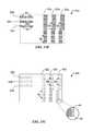
- FIG. 14illustrates a top down view of an alignment mark.
- FIG. 15Aillustrates a magnified view of one embodiment of an alignment mark.
- FIG. 15Billustrates a magnified view of another embodiment of an alignment mark, the alignment mark fragmented in a line space pattern.
- FIG. 15Cillustrates a magnified view of another embodiment of an alignment mark, the alignment mark fragmented in a square grid pattern.
- FIG. 16illustrates alignment marks staggered in a lock and key arrangement on an imprint field.
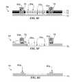
- a lithographic system 10used to form a relief pattern on a substrate 12 .
- Substrate 12may be coupled to substrate chuck 14 .
- substrate chuck 14is a vacuum chuck.
- Substrate chuck 14may be any chuck including, but not limited to, vacuum, pin-type, groove-type, electromagnetic, and/or the like. Exemplary chucks are described in U.S. Pat. No. 6,873,087, which is hereby incorporated by reference.
- Substrate 12 and substrate chuck 14may be further supported by stage 16 .
- Stage 16may provide motion along the x-, y-, and z-axes.
- Stage 16 , substrate 12 , and substrate chuck 14may also be positioned on a base (not shown).
- Template 18Spaced-apart from substrate 12 is a template 18 .
- Template 18generally includes a mesa 20 extending therefrom towards substrate 12 , mesa 20 having a patterning surface 22 thereon. Further, mesa 20 may be referred to as mold 20 .
- Template 18 and/or mold 20may be formed from such materials including, but not limited to, fused-silica, quartz, silicon, organic polymers, siloxane polymers, borosilicate glass, fluorocarbon polymers, metal, hardened sapphire, and/or the like.
- patterning surface 22comprises features defined by a plurality of spaced-apart recesses 24 and/or protrusions 26 , though embodiments of the present invention are not limited to such configurations. Patterning surface 22 may define any original pattern that forms the basis of a pattern to be formed on substrate 12 .
- Template 18may be coupled to chuck 28 .
- Chuck 28may be configured as, but not limited to, vacuum, pin-type, groove-type, electromagnetic, and/or other similar chuck types. Exemplary chucks are further described in U.S. Pat. No. 6,873,087, which is hereby incorporated by reference. Further, chuck 28 may be coupled to imprint head 30 such that chuck 28 and/or imprint head 30 may be configured to facilitate movement of template 18 .
- System 10may further comprise a fluid dispense system 32 .
- Fluid dispense system 32may be used to deposit polymerizable material 34 on substrate 12 .
- Polymerizable material 34may be positioned upon substrate 12 using techniques such as drop dispense, spin-coating, dip coating, chemical vapor deposition (CVD), physical vapor deposition (PVD), thin film deposition, thick film deposition, and/or the like.
- Polymerizable material 34may be disposed upon substrate 12 before and/or after a desired volume is defined between mold 22 and substrate 12 depending on design considerations.
- Polymerizable material 34may comprise a monomer mixture as described in U.S. Pat. No. 7,157,036 and U.S. Patent Publication No. 2005/0187339, all of which are hereby incorporated by reference.
- system 10may further comprise an energy source 38 coupled to direct energy 40 along path 42 .
- Imprint head 30 and stage 16may be configured to position template 18 and substrate 12 in superimposition with path 42 .
- System 10may be regulated by a processor 54 in communication with stage 16 , imprint head 30 , fluid dispense system 32 , and/or source 38 , and may operate on a computer readable program stored in memory 56 .
- Either imprint head 30 , stage 16 , or bothmay vary a distance between mold 20 and substrate 12 to define a desired volume therebetween that is filled by polymerizable material 34 .
- imprint head 30may apply a force to template 18 such that mold 20 contacts polymerizable material 34 .
- source 38produces energy 40 , e.g., broadband ultraviolet radiation, causing polymerizable material 34 to solidify and/or cross-link conforming to shape of a surface 44 of substrate 12 and patterning surface 22 , defining a patterned layer 46 on substrate 12 .
- Patterned layer 46may comprise a residual layer 48 and a plurality of features shown as protrusions 50 and recessions 52 , with protrusions 50 having thickness t 1 and residual layer having a thickness t 2 .
- One manner in which to locate the polymerizable material 34 between template 18 and substrate 12may be by depositing a plurality of droplets of polymerizable material 34 on the surface of substrate 12 . Thereafter, polymerizable material 34 may be concurrently contacted by both template 18 and substrate 12 , spreading polymerizable material 34 on the surface of substrate 12 . During this process, orientation of template 18 to substrate 12 may become a factor.
- template 18 and/or substrate 12may include alignment marks 60 to provide suitable orientation. Alignment marks 60 may be formed on patterning surface 22 of template 18 and/or substrate 12 or etched into template 18 and/or substrate 12 as illustrated in FIG. 3B .
- desired alignment between template 18 and substrate 12occurs upon alignment mark 60 of the template 18 being in superimposition with alignment mark 90 of the substrate 12 .
- desired alignment between template 18 and substrate 12has not occurred, shown by the two marks being offset a distance O.
- offset Ois shown as being a linear offset in one direction, it should be understood that the offset may be linear along two directions shown as O 1 and O 2 in FIG. 5 .
- the offset between template 18 and substrate 12may also consist of an angular offset, shown in FIG. 6 as angle ⁇ .
- Multiple alignment masksmay also have other offsets in combination (e.g., magnification, skew, trapezoidal distortions, and the like).
- the material comprising template 18may have the same indices of refraction as polymerizable material 34 . Even further, the indices of refraction may be in the range of wavelengths used for the alignment process. Alignment marks 60 of template 18 having the same indices of refraction as polymerizable material 34 may cause alignment marks 60 of template 18 to be invisible during the alignment process when in contact with polymerizable material 34 . Invisibility of alignment marks 60 of template 18 may hinder the alignment process between template 18 and substrate 12 for patterning of polymerizable material 34 .
- Isolation of the alignment marks 60 of template 18 and/or substrate 12 from polymerizable material 34may facilitate visibility during the alignment process.
- a moat(not shown) may be etched into template 18 during the pedestal making process to isolate polymerizable material 34 from alignment marks 60 .
- Moats, channels, and other similar featuresare further described in U.S. Ser. No. 10/917,761, U.S. Pat. No. 7,077,992, U.S. Pat. No. 7,041,604, U.S. Pat. No. 6,916,584, and U.S. Pat. No. 7,252,777, which are hereby incorporated by reference.
- the minimum required space needed for such featuresmay generally be large due to the width of the moat and/or channel, and the distance that may be needed between alignment marks 60 and the edges of mold 20 .
- alignment marks 60may be formed to provide visibility during the alignment process.
- alignment marks having characteristics and formations as described hereinmay be provided in substrate 12 .
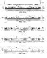
- FIGS. 7A-7Eillustrate side views of embodiments of template 18 a that include alignment marks 60 a visible during the alignment process.
- alignment marks 60 amay be formed of a high contrast material.
- High contrast materialsmay include, but are not limited to, tantalum, tantalum nitride, tungsten, silicon carbide, amorphous silicon, chromium, chromium nitride, molybdenum, molybdenum silicide, titanium, titanium nitride, combinations of these materials and/or the like.
- High contrast materialsmay have an optical density suitable for use in alignment marks 60 a when provided at thicknesses less than the thickness of patterned layer 48 (e.g., less than 25 nm) illustrated in FIG. 2 .
- a layer of high contrast material in alignment mark 60 amay be such that at least a portion of alignment mark 60 a resides in polymerizable material 34 during formation of patterned layer 48 , and thus alignment mark 60 a may not limit proximity of substrate 12 to surface of template 18 .
- Alignment marks 60 amay be visible during the alignment process with or without the use of a trench or other similar isolation means. Alignment marks 60 a may be embedded within mold 20 , as illustrated in FIG. 7A , positioned on patterning surface 22 a of mold 20 , as illustrated by FIG. 7C , or a combination of both on patterning surface 22 a and imbedded within mold 20 .
- FIGS. 7A-7Eillustrate variations of template 18 a having visible alignment marks 60 a during the patterning process.
- a first portion 61 a of alignment marks 60 amay be formed of high contrast material while a second portion 63 a is substantially absent of high contrast material.
- the first portionmay be integral to alignment mark 60 a , or as illustrated in FIGS. 7A and 7B , the first portion may be localized.
- the first portion having high contrast materialmay be localized at patterning surface 22 a .
- high contrast materialmay be used to substantially coat alignment marks 60 a.
- high contrast materialmay be applied throughout template 18 b and not localized on alignment marks 60 a .
- high contrast materialmay coat patterning surface 48 a of template 18 b .
- high contrast materialmay be integral within template 18 b.
- FIGS. 8A-8Killustrate simplified side views of exemplary formation of template 18 a having high-contrast alignment marks 60 a .
- template 18 amay be formed from a multi-layer substrate 64 and comprise mesa 20 a having high-contrast alignment marks 60 a .
- Contrast material used to form alignment marks 60 amay be generally compatible with the imprint process used currently within the industry, and as such, contrast material may be cleaned after imprinting without substantial damage.
- formation of alignment marks 60 amay be within the same processing step as formation of features 24 a and/or 24 b . Formation within the same processing step may reduce overlay alignment error.
- multi-layer substrate 64may generally comprise a substrate layer 70 , a contrast material layer 72 , a hard mask layer 74 , and resist 76 .
- Substrate layer 70may be formed from materials including, but not limited to, quartz, silicon, organic polymers, siloxane polymers, borosilicate glass, fluorocarbon polymers, metal, hardened sapphire, and/or the like.
- Hard mask layer 74may be formed from materials including, but not limited to, tantalum, tantalum nitride, tungsten, silicon carbide, amorphous silicon, chromium, chromium nitride, molybdenum, molybdenum silicide, titanium, titanium nitride, and/or the like.
- Contrast material layer 72may be formed from materials including, but not limited to, tantalum, tantalum nitride, tungsten, silicon carbide, amorphous silicon, chromium, chromium nitride, molybdenum, molybdenum silicide, titanium, titanium nitride, combinations of these materials and/or the like. It should be noted contrast material layer 72 may serve a dual purpose in that contrast material layer 72 may provide high contrast material for visibility of alignment mark during patterning of substrate 12 and also serve as a hard mask layer in addition to or in lieu of hard mask layer 74 .
- contrast material layer 72 , hard mask layer 74 , and resist 76may be patterned to include primary features (e.g., recessions 24 a and protrusions 26 a ) and/or alignment marks 60 a .
- Multi-layer substrate 64may be further substantially removed of resist 76 and recoated with resist 78 as shown in FIG. 8C .
- resist 76may be removed using techniques including, but not limited to, resist strip and solvent wet processes, oxygen ash etch processes, UV ozonated processes, ozonated water, and the like. It should be noted that the multi-layer substrate 64 may be coated with resist 78 without complete removal of resist 76 .
- FIG. 8Dat least a portion of features 24 a and 26 a of multi-layer substrate 64 may be exposed, as resist 78 substantially blocks (e.g., masks) processing of alignment marks 60 a while the remaining features 24 a and 26 a are unblocked (e.g., unmasked).
- resist 78substantially blocks (e.g., masks) processing of alignment marks 60 a while the remaining features 24 a and 26 a are unblocked (e.g., unmasked).
- steps shown in FIGS. 8C and 8Dmay be optional.
- steps shown in FIGS. 8C and 8Dmay be used to limit the depth of alignment marks 60 a.
- features 24 a and 26 a of multi-layer substrate 64may be further etched into substrate 70 as illustrated in FIG. 8E .
- resist 78may substantially block the etch process from altering alignment marks 60 a.
- the multi-layered substrate 64may further be substantially removed of contrast material layer 72 and hard mask layer 74 .
- Contrast material layer 72 and/or hard mask layer 74may be removed using techniques including, but not limited to, wet etching, RIE, ERIE, ICP, plasma etching, dry isotropic etching, and the like.
- chromium based high contrast materialsmay be removed by wet etching with high selectivity using chromium etchants, such as, for example, Cr7S and Cr9S Chromium based films may also be removed with chlorine and O 2 based plasma processes.
- the removal processmay selectively remove contrast material layer 72 and/or hard mask layer 74 with minimal effects on features 24 a and/or 26 a .
- resist 78may substantially block the removal process from altering alignment marks 60 a . Protection provided by resist 78 during removal of contrast material layer 72 and/or hard mask layer 74 may provide alignment marks 60 a to be independent from depth of the features 24 a and 26 a .
- alignment mark 60 amay have a depth D 1 while protrusions 26 a may have a depth D 2 , wherein D 1 ⁇ D 2 .
- the step shown in FIG. 8Fmay be optional as contrast material layer 72 and/or hard mask layer 74 may remain over features 24 and 26 .
- multi-layer substrate 64may be further substantially stripped of resist 78 . Additionally, hard mask layer 74 , shielded by resist 78 , may be substantially stripped to expose at least a portion of alignment marks 60 a.
- additional processing of multi-layer substrate 64may provide sidewalls 80 a functioning to assist in substantially confining polymerizable material 34 between template 18 and the substrate 12 in the desired volume during polymerization and/or cross-linking as described above (see FIG. 1 ).
- sidewalls 80 amay be formed by methods further described in U.S. patent application Ser. No. 11/762,378, now U.S. Pat. No. 7,473,090, which is hereby incorporated by reference.
- the resulting template 18comprises mesa 20 having alignment marks 60 a formed of contrast material.
- Sidewalls 80 amay be formed prior to patterning of alignment marks 60 a and/or formed subsequent to patterning of alignment marks 60 a .
- sidewalls 80 amay be formed prior to patterning of alignment marks 60 a such that sidewalls 80 a may be formed from a single substrate in contrast to multi-layer substrate 64 which may simplify formation.
- FIGS. 8H-8Killustrates an exemplary process wherein sidewalls 80 a may be formed in multi-layer substrate 64 subsequent to patterning of alignment marks 60 a .
- Multi-layer substrate 64may be coated with a resist 82 and a hard mask layer 84 as illustrated by FIG. 8H . Portions of resist 82 and hard mask layer 84 are removed such that alignment marks 60 a and features 24 a and 26 a remain substantially shielded by resist 82 and hard mask layer 84 as illustrated by FIG. 8I .
- sidewalls 80 amay be formed.
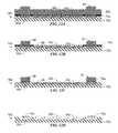
- an protective layer 87may be used to form alignment marks 60 b that are visible during the alignment process.
- Protective layer 87may be localized within alignment mark 60 b , or as illustrated in FIGS. 9A and 9B , protective layer 87 may coat alignment marks 60 b .
- a first portion 61 b of alignment mark 60 bmay include high contrast material
- a second portion 63 b of alignment mark 60 bmay be substantially free of high contrast material
- protective layer 87may coat first portion 61 b and second portion 63 b of alignment mark 60 b.
- FIGS. 10A-10Killustrate simplified side views of another exemplary formation of template 18 b from a multi-layered substrate 86 b having a protective layer 87 (e.g., oxide layer).
- the resulting template 18 b(see FIG. 10H ) formed from multi-layer substrate 86 b comprises mesa 20 b having high-contrast alignment marks 60 b . Additionally, formation of alignment marks 60 b may be within the same processing step as formation of features 24 b and/of 26 b . Formation within the same processing step may reduce overlay alignment error.
- multi-layer substrate 86 bmay comprise a substrate layer 70 b , a hard mask layer 74 b , and a resist layer 76 b , and may be patterned to include features 24 b and 26 b and/or alignment marks 60 b .
- Multi-layer substrate 86may be further substantially stripped of resist 76 b as illustrated in FIG. 10B and recoated with protective layer 87 (e.g., oxide layer), as illustrated in FIG. 10C .
- protective layer 87e.g., oxide layer
- a second resist layer 88 bmay then be placed to substantially shield alignment marks 60 b as illustrated in FIG. 10D .
- Second resist layer 88 bmay be selectively etched such that a portion of second resist layer 88 b protects alignment marks 60 b as illustrated in FIG. 10E .
- features 24 b and 26 bmay be further etched into substrate 70 .
- hard mask layer 74 bmay be removed.
- hard mask layer 74 bmay be removed using techniques including, but not limited to, dry isotropic etching (e.g., xenon diflouride gas), wet etching (e.g., KOH), and the like.
- the multi-layer substrate 86may be substantially stripped of resist 88 exposing alignment marks 60 b to provide template 18 b having alignment marks 60 b wherein at least a portion of alignment marks 60 may be formed of high contrast material.
- Additional processing of template 18 bmay provide sidewalls functioning to assist in substantially confining polymerizable material 34 between template 18 b and substrate 12 in the desired volume during polymerization and/or cross-linking as described above (see FIG. 1 ).
- sidewalls 80 bmay be formed by methods further described in U.S. Pat. No. 7,473,090 which is hereby incorporated by reference. It should be noted sidewalls may be formed prior to formation of features 24 b and 26 b and/or alignment marks 60 b or sidewalls may be formed subsequent to formation of features 24 b and 26 b and/or alignment marks 60 b.
- Alignment marks having high contrast materialmay also be formed during replica patterning of device to have substantially the same pattern as a master template. Forming master templates using e-beam lithography or other methods may be time consuming and expensive. As such, replicas of the master template may be used as working templates.
- FIGS. 11A-11E , FIGS. 12A-12D and FIGS. 13A-13Dillustrate exemplary replication processes to form replica templates 18 d from master template 18 c .
- Replica templates 18 dinclude high contrast alignment marks 60 c.
- any standard photomask processmay be used to create master template 18 c including, but not limited to, variable shaped electron beam, Gaussian electron beam, laser writing and other similar processes. Master template 18 c may then be used to form features 24 c and 26 c , as well as alignment marks 60 c within substrate 12 c as illustrated in FIG. 11A .
- imprint lithography techniquessuch as those described herein, may be used to form features 24 c and 26 c , as well as alignment marks 60 c within substrate 12 c.
- Substrate 12 cmay include substrate layer 70 c , resist layer 76 c and a temporary hard mask layer 74 c .
- Hard mask layer 74 cmay be used to improve resist exposure and etch pattern transfer depending on design considerations. It should be noted, and as described in detail above, hard mask layer 74 c may be formed of high contrast material. Alternatively, a separate high contrast material layer may be used in conjunction with hard mask layer 74 c to form replica template 18 d.
- features 24 c and 26 c and/or alignment marks 60 cmay be further etched in hard mask layer 74 c and/or substrate layer 70 c . Portions of hard mask layer 74 c may removed, as illustrated in FIG. 11C , and features 24 c and 26 c and/or alignment marks 60 c further etched into substrate layer 70 c . Resist may be removed to form replica template 18 d having alignment marks 60 c with at least a portion of alignment marks 60 c being formed of high contrast material.
- Replica template 18 dmay be further processed localizing high contrast material.
- replica template 18 dmay be further processed such that only alignment marks 60 c include high contrast material.
- FIGS. 12A-12Dillustrate an exemplary process for localizing high contrast material in alignment marks 60 c.
- a second resist layer 88 cmay be positioned (e.g., imprinted) on replica template 18 d .
- Second resist layer 88 cmay include one or more alignment blocks 91 .
- Alignment blocks 91may be positioned in superimposition with alignment marks 60 c to substantially block removal of high contrast material from alignment marks 60 during etching and/or stripping.
- second resist layer 88 cmay be stripped exposing at least a portion of hard mask layer 74 c of features 26 c .
- Etchingmay remove a first portion of hard mask layer 74 c as illustrated in FIG. 12C while alignment blocks 91 may block etching of at least a second portion of hard mask layer 74 c .
- alignment blocks 91may block alignment marks 60 c from having hard mask layer 74 c removed.
- Resist layer 88 cmay then be removed providing replica template 18 d having high contrast material localized in alignment marks 60 c.
- FIGS. 13A-13Dillustrate another exemplary process for localizing high contrast material in alignment marks 60 c of template 18 d .
- a second resist layer 88 dmay be may be positioned on replica template 18 d using techniques such as spin-coating.
- Second resist layer 88 dmay be developed to form alignment blocks 91 a that substantially block alignment marks 60 c from further processing.
- hard mask layer 74 cmay be stripped while alignment blocks 91 a substantially block stripping of hard mask layer 74 c of alignment marks 60 c .
- Resist layer 88 dmay then be removed providing replica template 18 d having high contrast material localized in alignment marks 60 c.
- Alignment marks 60 a and/or 60 b formed of contrast materialmay provide enough visibility to perform alignment even in the presence of polymerizable material 34 .
- features 92may be altered in an effort to pass more UV wavelength, while providing longer wavelengths of energy used for alignment to be absorbed, reflected, and/or diffracted.
- alignment marks 60 amay generally have features 92 around 1 ⁇ m in width. These features 92 may be fragmented into small repeating sub-features 94 ranging in size from 50 nm to 200 nm. Fragmentation of alignment marks 60 a may reduce the contact area of the contrast material to polymerizable material 34 (see FIG. 1 ) during curing.
- FIGS. 15B and 15Cillustrate two embodiments of alignment marks 60 a and 60 b having altered pitch.
- features 92 a of alignment mark 60 aare fragmented by line space to provide repeating line sub-features 94 ranging in size from 50 nm to 200 nm.
- features 92 b of alignment mark 60 bare fragmented in square grid pattern sub-features 94 providing repeating squares ranging in size from 50 nm to 200 nm.
- Space allocation for alignment marks 60may be further reduced by staggering alignment marks 60 .
- alignments marks 60are staggered in a lock and key arrangement on an imprint field 96 .
- the staggered layout on the imprint field 96may utilize the same horizontal scribe spacing for alignment marks 60 placed in the top and bottom perimeter edges of the field 96 .
- the same vertical scribe spacingmay be used for the alignment marks 60 placed in the left and right perimeter edges of the field 96 .
- the staggered layoutreduces the scribe width while maintaining alignment marks 60 in each of the four corners 98 a , 98 b , 98 c , and 98 d of each section 100 a - 100 d of the imprint field 96 .
- alignment marks 60 in corners 98 b and 98 d of section 100 aalign in a lock and key arrangement with alignment marks 60 in corners 98 a and 98 c of section 100 b .
- alignment marks 60 in corners 98 c and 98 d of section 100 aalign in a lock and key arrangement with alignment marks 60 in corners 98 a and 98 b of section 100 c.
- the staggered layout on the imprint field 96may include the use of alignment marks 60 formed of contrast material. Additionally, or in lieu of the high-contrast material, the staggered layout on the imprint field 96 may include the use of moats as described in U.S. patent application Ser. No. 10/917,761, which is hereby incorporated by reference.
Landscapes
- Physics & Mathematics (AREA)
- General Physics & Mathematics (AREA)
- Engineering & Computer Science (AREA)
- Chemical & Material Sciences (AREA)
- Nanotechnology (AREA)
- Crystallography & Structural Chemistry (AREA)
- Condensed Matter Physics & Semiconductors (AREA)
- Manufacturing & Machinery (AREA)
- Mathematical Physics (AREA)
- Theoretical Computer Science (AREA)
- Exposure Of Semiconductors, Excluding Electron Or Ion Beam Exposure (AREA)
- Shaping Of Tube Ends By Bending Or Straightening (AREA)
Abstract
Description
Claims (17)
Priority Applications (2)
| Application Number | Priority Date | Filing Date | Title |
|---|---|---|---|
| US12/464,487US8012395B2 (en) | 2006-04-18 | 2009-05-12 | Template having alignment marks formed of contrast material |
| PCT/US2009/002959WO2010042140A2 (en) | 2008-10-10 | 2009-05-13 | Template having alignment marks formed of contrast material |
Applications Claiming Priority (4)
| Application Number | Priority Date | Filing Date | Title |
|---|---|---|---|
| US79275006P | 2006-04-18 | 2006-04-18 | |
| US11/693,236US7547398B2 (en) | 2006-04-18 | 2007-03-29 | Self-aligned process for fabricating imprint templates containing variously etched features |
| US10430008P | 2008-10-10 | 2008-10-10 | |
| US12/464,487US8012395B2 (en) | 2006-04-18 | 2009-05-12 | Template having alignment marks formed of contrast material |
Related Parent Applications (1)
| Application Number | Title | Priority Date | Filing Date |
|---|---|---|---|
| US11/693,236Continuation-In-PartUS7547398B2 (en) | 2006-04-18 | 2007-03-29 | Self-aligned process for fabricating imprint templates containing variously etched features |
Publications (2)
| Publication Number | Publication Date |
|---|---|
| US20090250840A1 US20090250840A1 (en) | 2009-10-08 |
| US8012395B2true US8012395B2 (en) | 2011-09-06 |
Family
ID=40940363
Family Applications (1)
| Application Number | Title | Priority Date | Filing Date |
|---|---|---|---|
| US12/464,487Active2027-06-02US8012395B2 (en) | 2006-04-18 | 2009-05-12 | Template having alignment marks formed of contrast material |
Country Status (2)
| Country | Link |
|---|---|
| US (1) | US8012395B2 (en) |
| WO (1) | WO2010042140A2 (en) |
Cited By (10)
| Publication number | Priority date | Publication date | Assignee | Title |
|---|---|---|---|---|
| US20110192302A1 (en)* | 2010-02-05 | 2011-08-11 | Molecular Imprints, Inc. | Templates Having High Contrast Alignment Marks |
| JP2014011254A (en)* | 2012-06-28 | 2014-01-20 | Dainippon Printing Co Ltd | Alignment mark, template with the mark, and manufacturing method of the template |
| US20150165655A1 (en)* | 2011-04-25 | 2015-06-18 | Canon Nanotechnologies, Inc. | Optically Absorptive Material for Alignment Marks |
| US9377683B2 (en) | 2013-03-22 | 2016-06-28 | HGST Netherlands B.V. | Imprint template with optically-detectable alignment marks and method for making using block copolymers |
| US9811671B1 (en) | 2000-05-24 | 2017-11-07 | Copilot Ventures Fund Iii Llc | Authentication method and system |
| US9846814B1 (en) | 2008-04-23 | 2017-12-19 | Copilot Ventures Fund Iii Llc | Authentication method and system |
| US10114284B2 (en) | 2013-08-05 | 2018-10-30 | Toshiba Memory Corporation | Method for designing mask set, recording medium, template, and method for manufacturing template |
| US10921706B2 (en) | 2018-06-07 | 2021-02-16 | Canon Kabushiki Kaisha | Systems and methods for modifying mesa sidewalls |
| US10990004B2 (en) | 2018-07-18 | 2021-04-27 | Canon Kabushiki Kaisha | Photodissociation frame window, systems including a photodissociation frame window, and methods of using a photodissociation frame window |
| US20210350047A1 (en)* | 2019-01-30 | 2021-11-11 | Canon Kabushiki Kaisha | Simulation method and simulation apparatus |
Families Citing this family (16)
| Publication number | Priority date | Publication date | Assignee | Title |
|---|---|---|---|---|
| US20100092599A1 (en)* | 2008-10-10 | 2010-04-15 | Molecular Imprints, Inc. | Complementary Alignment Marks for Imprint Lithography |
| US8432548B2 (en)* | 2008-11-04 | 2013-04-30 | Molecular Imprints, Inc. | Alignment for edge field nano-imprinting |
| US8231821B2 (en)* | 2008-11-04 | 2012-07-31 | Molecular Imprints, Inc. | Substrate alignment |
| NL2005266A (en)* | 2009-10-28 | 2011-05-02 | Asml Netherlands Bv | Imprint lithography. |
| NL2005975A (en)* | 2010-03-03 | 2011-09-06 | Asml Netherlands Bv | Imprint lithography. |
| EP2618978B1 (en)* | 2010-09-24 | 2016-11-09 | Canon Nanotechnologies, Inc. | High contrast alignment marks through multiple stage imprinting |
| JP5831012B2 (en)* | 2011-07-27 | 2015-12-09 | 大日本印刷株式会社 | Alignment mark for imprint, template provided with the mark, and manufacturing method thereof |
| US10124529B2 (en)* | 2013-12-10 | 2018-11-13 | Canon Nanotechnologies, Inc. | Imprint lithography template and method for zero-gap imprinting |
| JP6503211B2 (en)* | 2015-03-27 | 2019-04-17 | 旭化成株式会社 | Imprint molding mold and manufacturing method thereof |
| JP2016028442A (en)* | 2015-10-08 | 2016-02-25 | 大日本印刷株式会社 | template |
| CN105353592B (en)* | 2015-11-25 | 2018-09-21 | 武汉新芯集成电路制造有限公司 | A kind of photoetching process alignment methods |
| JP6308281B2 (en)* | 2016-10-21 | 2018-04-11 | 大日本印刷株式会社 | Template manufacturing method |
| US11194247B2 (en) | 2018-01-31 | 2021-12-07 | Canon Kabushiki Kaisha | Extrusion control by capillary force reduction |
| US11562924B2 (en)* | 2020-01-31 | 2023-01-24 | Canon Kabushiki Kaisha | Planarization apparatus, planarization process, and method of manufacturing an article |
| US11728173B2 (en)* | 2020-09-30 | 2023-08-15 | Taiwan Semiconductor Manufacturing Co., Ltd. | Masking layer with post treatment |
| US12085852B2 (en)* | 2021-12-27 | 2024-09-10 | Canon Kabushiki Kaisha | Template, method of forming a template, apparatus and method of manufacturing an article |
Citations (255)
| Publication number | Priority date | Publication date | Assignee | Title |
|---|---|---|---|---|
| US3503538A (en) | 1966-11-29 | 1970-03-31 | Bp Chem Int Ltd | Metering process and apparatus |
| US4022855A (en) | 1975-03-17 | 1977-05-10 | Eastman Kodak Company | Method for making a plastic optical element having a gradient index of refraction |
| US4070116A (en) | 1975-06-23 | 1978-01-24 | International Business Machines Corporation | Gap measuring device for defining the distance between two or more surfaces |
| US4208240A (en) | 1979-01-26 | 1980-06-17 | Gould Inc. | Method and apparatus for controlling plasma etching |
| US4364971A (en) | 1980-06-18 | 1982-12-21 | Felix Schoeller, Jr. Gmbh & Co. | Waterproof photographic paper and method of producing same |
| US4440804A (en) | 1982-08-02 | 1984-04-03 | Fairchild Camera & Instrument Corporation | Lift-off process for fabricating self-aligned contacts |
| US4512848A (en) | 1984-02-06 | 1985-04-23 | Exxon Research And Engineering Co. | Procedure for fabrication of microstructures over large areas using physical replication |
| US4521445A (en) | 1982-09-07 | 1985-06-04 | Energy Sciences, Inc. | Method and apparatus for electron curing on a cooled drum |
| JPS60111425A (en) | 1983-11-22 | 1985-06-17 | Toshiba Corp | How to form alignment marks |
| US4552832A (en) | 1982-03-06 | 1985-11-12 | Braun Aktiengesellschaft | Shear foil having protrusions on its skin-contacting surface thereof |
| US4576900A (en) | 1981-10-09 | 1986-03-18 | Amdahl Corporation | Integrated circuit multilevel interconnect system and method |
| US4637904A (en) | 1983-11-14 | 1987-01-20 | Rohm And Haas Company | Process for molding a polymeric layer onto a substrate |
| US4676868A (en) | 1986-04-23 | 1987-06-30 | Fairchild Semiconductor Corporation | Method for planarizing semiconductor substrates |
| US4707218A (en) | 1986-10-28 | 1987-11-17 | International Business Machines Corporation | Lithographic image size reduction |
| US4731155A (en) | 1987-04-15 | 1988-03-15 | General Electric Company | Process for forming a lithographic mask |
| US4737425A (en) | 1986-06-10 | 1988-04-12 | International Business Machines Corporation | Patterned resist and process |
| US4848911A (en) | 1986-06-11 | 1989-07-18 | Kabushiki Kaisha Toshiba | Method for aligning first and second objects, relative to each other, and apparatus for practicing this method |
| US4857477A (en) | 1986-09-18 | 1989-08-15 | Oki Electric Industry Co., Ltd. | Process for fabricating a semiconductor device |
| US4862019A (en) | 1988-04-20 | 1989-08-29 | Texas Instruments Incorporated | Single-level poly programmable bit circuit |
| US4866307A (en) | 1988-04-20 | 1989-09-12 | Texas Instruments Incorporated | Integrated programmable bit circuit using single-level poly construction |
| US4908298A (en) | 1985-03-19 | 1990-03-13 | International Business Machines Corporation | Method of creating patterned multilayer films for use in production of semiconductor circuits and systems |
| US4909151A (en) | 1986-11-10 | 1990-03-20 | Matsushita Electric Industrial Co., Ltd. | Method of forming an ink image and printing the formed image |
| US4919748A (en) | 1989-06-30 | 1990-04-24 | At&T Bell Laboratories | Method for tapered etching |
| US4921778A (en) | 1988-07-29 | 1990-05-01 | Shipley Company Inc. | Photoresist pattern fabrication employing chemically amplified metalized material |
| US4932358A (en) | 1989-05-18 | 1990-06-12 | Genus, Inc. | Perimeter wafer seal |
| US4936465A (en) | 1987-12-07 | 1990-06-26 | Zoeld Tibor | Method and apparatus for fast, reliable, and environmentally safe dispensing of fluids, gases and individual particles of a suspension through pressure control at well defined parts of a closed flow-through system |
| US4957663A (en) | 1986-02-13 | 1990-09-18 | U.S. Philips Corp. | Method of manufacturing optical components |
| US4959252A (en) | 1986-09-29 | 1990-09-25 | Rhone-Poulenc Chimie | Highly oriented thermotropic optical disc member |
| US4964945A (en) | 1988-12-09 | 1990-10-23 | Minnesota Mining And Manufacturing Company | Lift off patterning process on a flexible substrate |
| US4980316A (en) | 1988-07-20 | 1990-12-25 | Siemens Aktiengesellschaft | Method for producing a resist structure on a semiconductor |
| US5003062A (en) | 1990-04-19 | 1991-03-26 | Taiwan Semiconductor Manufacturing Co. | Semiconductor planarization process for submicron devices |
| US5028366A (en) | 1988-01-12 | 1991-07-02 | Air Products And Chemicals, Inc. | Water based mold release compositions for making molded polyurethane foam |
| US5028361A (en) | 1987-11-09 | 1991-07-02 | Takeo Fujimoto | Method for molding a photosensitive composition |
| US5053318A (en) | 1989-05-18 | 1991-10-01 | Shipley Company Inc. | Plasma processing with metal mask integration |
| US5073230A (en) | 1990-04-17 | 1991-12-17 | Arizona Board Of Regents Acting On Behalf Of Arizona State University | Means and methods of lifting and relocating an epitaxial device layer |
| US5110514A (en) | 1989-05-01 | 1992-05-05 | Soane Technologies, Inc. | Controlled casting of a shrinkable material |
| US5124089A (en) | 1986-12-25 | 1992-06-23 | Sony Corporation | Method of producing transmissive screens |
| US5126006A (en) | 1990-10-30 | 1992-06-30 | International Business Machines Corp. | Plural level chip masking |
| US5148037A (en) | 1988-09-09 | 1992-09-15 | Canon Kabushiki Kaisha | Position detecting method and apparatus |
| US5151754A (en) | 1989-10-06 | 1992-09-29 | Kabushiki Kaisha Toshiba | Method and an apparatus for measuring a displacement between two objects and a method and an apparatus for measuring a gap distance between two objects |
| FR2677043A1 (en) | 1991-05-29 | 1992-12-04 | Solems Sa | Process, device and apparatus for treating a substrate with a low-pressure plasma |
| US5212147A (en) | 1991-05-15 | 1993-05-18 | Hewlett-Packard Company | Method of forming a patterned in-situ high Tc superconductive film |
| US5232874A (en) | 1992-06-22 | 1993-08-03 | Micron Technology, Inc. | Method for producing a semiconductor wafer having shallow and deep buried contacts |
| US5240878A (en) | 1991-04-26 | 1993-08-31 | International Business Machines Corporation | Method for forming patterned films on a substrate |
| US5240550A (en) | 1990-09-21 | 1993-08-31 | U.S. Philips Corp. | Method of forming at least one groove in a substrate layer |
| US5244818A (en) | 1992-04-08 | 1993-09-14 | Georgia Tech Research Corporation | Processes for lift-off of thin film materials and for the fabrication of three dimensional integrated circuits |
| US5246880A (en) | 1992-04-27 | 1993-09-21 | Eastman Kodak Company | Method for creating substrate electrodes for flip chip and other applications |
| US5250472A (en) | 1992-09-03 | 1993-10-05 | Industrial Technology Research Institute | Spin-on-glass integration planarization having siloxane partial etchback and silicate processes |
| US5259926A (en) | 1991-09-24 | 1993-11-09 | Hitachi, Ltd. | Method of manufacturing a thin-film pattern on a substrate |
| US5277749A (en) | 1991-10-17 | 1994-01-11 | International Business Machines Corporation | Methods and apparatus for relieving stress and resisting stencil delamination when performing lift-off processes that utilize high stress metals and/or multiple evaporation steps |
| US5288436A (en) | 1990-11-06 | 1994-02-22 | Colloptics, Inc. | Methods of fabricating a collagen lenticule precursor for modifying the cornea |
| US5324683A (en) | 1993-06-02 | 1994-06-28 | Motorola, Inc. | Method of forming a semiconductor structure having an air region |
| US5328810A (en) | 1990-05-07 | 1994-07-12 | Micron Technology, Inc. | Method for reducing, by a factor or 2-N, the minimum masking pitch of a photolithographic process |
| US5330881A (en) | 1989-06-02 | 1994-07-19 | Digital Equipment Corp. | Microlithographic method for producing thick, vertically-walled photoresist patterns |
| US5348616A (en) | 1993-05-03 | 1994-09-20 | Motorola, Inc. | Method for patterning a mold |
| US5357122A (en) | 1991-09-05 | 1994-10-18 | Sony Corporation | Three-dimensional optical-electronic integrated circuit device with raised sections |
| US5362606A (en) | 1989-10-18 | 1994-11-08 | Massachusetts Institute Of Technology | Positive resist pattern formation through focused ion beam exposure and surface barrier silylation |
| US5362940A (en) | 1990-11-09 | 1994-11-08 | Litel Instruments | Use of Fresnel zone plates for material processing |
| US5364222A (en) | 1992-02-05 | 1994-11-15 | Tokyo Electron Limited | Apparatus for processing wafer-shaped substrates |
| US5366851A (en) | 1991-07-23 | 1994-11-22 | At&T Bell Laboratories | Device fabrication process |
| US5371822A (en) | 1992-06-09 | 1994-12-06 | Digital Equipment Corporation | Method of packaging and assembling opto-electronic integrated circuits |
| US5374327A (en) | 1992-04-28 | 1994-12-20 | Tokyo Electron Limited | Plasma processing method |
| US5376810A (en) | 1992-06-26 | 1994-12-27 | California Institute Of Technology | Growth of delta-doped layers on silicon CCD/S for enhanced ultraviolet response |
| US5422295A (en) | 1992-12-10 | 1995-06-06 | Samsung Electronics Co., Ltd. | Method for forming a semiconductor memory device having a vertical multi-layered storage electrode |
| US5424549A (en) | 1991-12-20 | 1995-06-13 | Board Of Supervisors Of Louisiana State University And Agricultural And Mechanical College | Scanning systems for high resolution e-beam and X-ray lithography |
| US5425848A (en) | 1993-03-16 | 1995-06-20 | U.S. Philips Corporation | Method of providing a patterned relief of cured photoresist on a flat substrate surface and device for carrying out such a method |
| US5431777A (en) | 1992-09-17 | 1995-07-11 | International Business Machines Corporation | Methods and compositions for the selective etching of silicon |
| US5434107A (en) | 1994-01-28 | 1995-07-18 | Texas Instruments Incorporated | Method for planarization |
| US5445195A (en) | 1992-07-15 | 1995-08-29 | Kim; Dae S. | Automatic computer-controlled liquid dispenser |
| US5449117A (en) | 1993-10-04 | 1995-09-12 | Technical Concepts, L.P. | Apparatus and method for controllably dispensing drops of liquid |
| US5451435A (en) | 1990-06-18 | 1995-09-19 | At&T Corp. | Method for forming dielectric |
| US5453157A (en) | 1994-05-16 | 1995-09-26 | Texas Instruments Incorporated | Low temperature anisotropic ashing of resist for semiconductor fabrication |
| US5458520A (en) | 1994-12-13 | 1995-10-17 | International Business Machines Corporation | Method for producing planar field emission structure |
| US5468542A (en) | 1985-12-23 | 1995-11-21 | General Electric Company | Method for production of a coated substrate with controlled surface characteristics |
| US5477058A (en)* | 1994-11-09 | 1995-12-19 | Kabushiki Kaisha Toshiba | Attenuated phase-shifting mask with opaque reticle alignment marks |
| US5480047A (en) | 1993-06-04 | 1996-01-02 | Sharp Kabushiki Kaisha | Method for forming a fine resist pattern |
| US5512131A (en) | 1993-10-04 | 1996-04-30 | President And Fellows Of Harvard College | Formation of microstamped patterns on surfaces and derivative articles |
| US5542605A (en) | 1994-04-07 | 1996-08-06 | Flow-Rite Controls, Ltd. | Automatic liquid dispenser |
| US5545367A (en) | 1992-04-15 | 1996-08-13 | Soane Technologies, Inc. | Rapid prototype three dimensional stereolithography |
| US5601641A (en) | 1992-07-21 | 1997-02-11 | Tse Industries, Inc. | Mold release composition with polybutadiene and method of coating a mold core |
| US5612068A (en) | 1994-03-14 | 1997-03-18 | Leybold Aktiengesellschaft | Apparatus for the transfer of substrates |
| US5628917A (en) | 1995-02-03 | 1997-05-13 | Cornell Research Foundation, Inc. | Masking process for fabricating ultra-high aspect ratio, wafer-free micro-opto-electromechanical structures |
| US5643364A (en) | 1994-11-30 | 1997-07-01 | Applied Materials, Inc. | Plasma chamber with fixed RF matching |
| US5654238A (en) | 1995-08-03 | 1997-08-05 | International Business Machines Corporation | Method for etching vertical contact holes without substrate damage caused by directional etching |
| US5669303A (en) | 1996-03-04 | 1997-09-23 | Motorola | Apparatus and method for stamping a surface |
| US5736424A (en) | 1987-02-27 | 1998-04-07 | Lucent Technologies Inc. | Device fabrication involving planarization |
| US5753014A (en) | 1993-11-12 | 1998-05-19 | Van Rijn; Cornelis Johannes Maria | Membrane filter and a method of manufacturing the same as well as a membrane |
| US5772905A (en) | 1995-11-15 | 1998-06-30 | Regents Of The University Of Minnesota | Nanoimprint lithography |
| US5776748A (en) | 1993-10-04 | 1998-07-07 | President And Fellows Of Harvard College | Method of formation of microstamped patterns on plates for adhesion of cells and other biological materials, devices and uses therefor |
| US5804474A (en) | 1996-04-10 | 1998-09-08 | Murata Manufacturing Co., Ltd. | Method for forming a V-shaped gate electrode in a semiconductor device, and the structure of the electrode |
| US5812629A (en) | 1997-04-30 | 1998-09-22 | Clauser; John F. | Ultrahigh resolution interferometric x-ray imaging |
| US5817579A (en) | 1997-04-09 | 1998-10-06 | Vanguard International Semiconductor Corporation | Two step plasma etch method for forming self aligned contact |
| US5820769A (en) | 1995-05-24 | 1998-10-13 | Regents Of The University Of Minnesota | Method for making magnetic storage having discrete elements with quantized magnetic moments |
| US5843363A (en) | 1995-03-31 | 1998-12-01 | Siemens Aktiengesellschaft | Ablation patterning of multi-layered structures |
| US5849222A (en) | 1995-09-29 | 1998-12-15 | Johnson & Johnson Vision Products, Inc. | Method for reducing lens hole defects in production of contact lens blanks |
| US5849209A (en) | 1995-03-31 | 1998-12-15 | Johnson & Johnson Vision Products, Inc. | Mold material made with additives |
| US5858580A (en) | 1997-09-17 | 1999-01-12 | Numerical Technologies, Inc. | Phase shifting circuit manufacture method and apparatus |
| US5888650A (en) | 1996-06-03 | 1999-03-30 | Minnesota Mining And Manufacturing Company | Temperature-responsive adhesive article |
| US5895263A (en) | 1996-12-19 | 1999-04-20 | International Business Machines Corporation | Process for manufacture of integrated circuit device |
| US5900160A (en) | 1993-10-04 | 1999-05-04 | President And Fellows Of Harvard College | Methods of etching articles via microcontact printing |
| US5907782A (en) | 1998-08-15 | 1999-05-25 | Acer Semiconductor Manufacturing Inc. | Method of forming a multiple fin-pillar capacitor for a high density dram cell |
| US5926690A (en) | 1997-05-28 | 1999-07-20 | Advanced Micro Devices, Inc. | Run-to-run control process for controlling critical dimensions |
| US5948570A (en) | 1995-05-26 | 1999-09-07 | Lucent Technologies Inc. | Process for dry lithographic etching |
| US5948470A (en) | 1997-04-28 | 1999-09-07 | Harrison; Christopher | Method of nanoscale patterning and products made thereby |
| US5974150A (en) | 1997-09-30 | 1999-10-26 | Tracer Detection Technology Corp. | System and method for authentication of goods |
| US5983906A (en) | 1997-01-24 | 1999-11-16 | Applied Materials, Inc. | Methods and apparatus for a cleaning process in a high temperature, corrosive, plasma environment |
| US6046056A (en) | 1996-06-28 | 2000-04-04 | Caliper Technologies Corporation | High throughput screening assay systems in microscale fluidic devices |
| US6048799A (en) | 1987-02-27 | 2000-04-11 | Lucent Technologies Inc. | Device fabrication involving surface planarization |
| US6067144A (en) | 1996-10-23 | 2000-05-23 | Kabushiki Kaisha Toshiba | LCD cell having two supporting gap members different in height |
| US6074827A (en) | 1996-07-30 | 2000-06-13 | Aclara Biosciences, Inc. | Microfluidic method for nucleic acid purification and processing |
| US6150680A (en) | 1998-03-05 | 2000-11-21 | Welch Allyn, Inc. | Field effect semiconductor device having dipole barrier |
| US6180239B1 (en) | 1993-10-04 | 2001-01-30 | President And Fellows Of Harvard College | Microcontact printing on surfaces and derivative articles |
| US6218316B1 (en) | 1998-10-22 | 2001-04-17 | Micron Technology, Inc. | Planarization of non-planar surfaces in device fabrication |
| US6242363B1 (en) | 1999-08-11 | 2001-06-05 | Adc Telecommunications, Inc. | Method of etching a wafer layer using a sacrificial wall to form vertical sidewall |
| US6245213B1 (en) | 1996-09-06 | 2001-06-12 | Obducat Ab | Method for anisotropic etching of structures in conducting materials |
| US6274294B1 (en) | 1999-02-03 | 2001-08-14 | Electroformed Stents, Inc. | Cylindrical photolithography exposure process and apparatus |
| US6309580B1 (en) | 1995-11-15 | 2001-10-30 | Regents Of The University Of Minnesota | Release surfaces, particularly for use in nanoimprint lithography |
| US6326627B1 (en) | 2000-08-02 | 2001-12-04 | Archimedes Technology Group, Inc. | Mass filtering sputtered ion source |
| US6329256B1 (en) | 1999-09-24 | 2001-12-11 | Advanced Micro Devices, Inc. | Self-aligned damascene gate formation with low gate resistance |
| US6334960B1 (en) | 1999-03-11 | 2002-01-01 | Board Of Regents, The University Of Texas System | Step and flash imprint lithography |
| US6337262B1 (en) | 2000-03-06 | 2002-01-08 | Chartered Semiconductor Manufacturing Ltd. | Self aligned T-top gate process integration |
| US6348999B1 (en) | 1995-05-10 | 2002-02-19 | Epigem Limited | Micro relief element and preparation thereof |
| US6355198B1 (en) | 1996-03-15 | 2002-03-12 | President And Fellows Of Harvard College | Method of forming articles including waveguides via capillary micromolding and microtransfer molding |
| US20020038916A1 (en) | 1998-12-23 | 2002-04-04 | 3M Innovative Properties Company | Method for precise molding and alignment of structures on a substrate using a stretchable mold |
| US20020042027A1 (en) | 1998-10-09 | 2002-04-11 | Chou Stephen Y. | Microscale patterning and articles formed thereby |
| US6376379B1 (en) | 2000-02-01 | 2002-04-23 | Chartered Semiconductor Manufacturing Ltd. | Method of hard mask patterning |
| US6379573B1 (en) | 1999-07-13 | 2002-04-30 | University Of Honolulu | Self-limiting isotropic wet etching process |
| US6383928B1 (en) | 1999-09-02 | 2002-05-07 | Texas Instruments Incorporated | Post copper CMP clean |
| US6388253B1 (en) | 1999-06-29 | 2002-05-14 | Applied Materials, Inc. | Integrated critical dimension control for semiconductor device manufacturing |
| US6387783B1 (en) | 1999-04-26 | 2002-05-14 | International Business Machines Corporation | Methods of T-gate fabrication using a hybrid resist |
| US6387330B1 (en) | 2000-04-12 | 2002-05-14 | George Steven Bova | Method and apparatus for storing and dispensing reagents |
| US6391217B2 (en) | 1999-12-23 | 2002-05-21 | University Of Massachusetts | Methods and apparatus for forming submicron patterns on films |
| US6391798B1 (en) | 1987-02-27 | 2002-05-21 | Agere Systems Guardian Corp. | Process for planarization a semiconductor substrate |
| US20020094496A1 (en) | 2000-07-17 | 2002-07-18 | Choi Byung J. | Method and system of automatic fluid dispensing for imprint lithography processes |
| US6423207B1 (en) | 1998-03-05 | 2002-07-23 | Obducat Ab | Method and apparatus for etching |
| US20020110992A1 (en) | 2001-02-12 | 2002-08-15 | Lam Research Corporation | Use of hydrocarbon addition for the elimination of micromasking during etching |
| US20020111036A1 (en) | 2001-02-12 | 2002-08-15 | Lam Research Corporation | Unique process chemistry for etching organic low-k materials |
| US20020132482A1 (en) | 2000-07-18 | 2002-09-19 | Chou Stephen Y. | Fluid pressure imprint lithography |
| US20020168578A1 (en) | 1996-09-18 | 2002-11-14 | Numerical Technologies, Inc. | Phase shifting circuit manufacture method and apparatus |
| US20020170880A1 (en) | 2001-03-22 | 2002-11-21 | Yong Chen | Scanning probe based lithographic alignment |
| US6495907B1 (en) | 1994-09-30 | 2002-12-17 | Texas Instruments Incorporated | Conductor reticulation for improved device planarity |
| US20020191141A1 (en) | 2001-06-14 | 2002-12-19 | Bing-Jei Liao | Panel with a blocker for separating sealant and liquid crystal layer |
| US6498640B1 (en) | 1999-12-30 | 2002-12-24 | Koninklijke Philips Electronics N.V. | Method to measure alignment using latent image grating structures |
| US6503829B2 (en) | 2000-08-19 | 2003-01-07 | Samsung Electronics Co., Ltd. | Metal via contact of a semiconductor device and method for fabricating the same |
| US6514672B2 (en) | 1999-06-17 | 2003-02-04 | Taiwan Semiconductor Manufacturing Company | Dry development process for a bi-layer resist system |
| US20030025895A1 (en) | 2001-08-03 | 2003-02-06 | Michael Binnard | Apparatus and methods for detecting tool-induced shift in microlithography apparatus |
| US6517995B1 (en) | 1999-09-14 | 2003-02-11 | Massachusetts Institute Of Technology | Fabrication of finely featured devices by liquid embossing |
| US6517977B2 (en) | 2001-03-28 | 2003-02-11 | Motorola, Inc. | Lithographic template and method of formation and use |
| US6518189B1 (en) | 1995-11-15 | 2003-02-11 | Regents Of The University Of Minnesota | Method and apparatus for high density nanostructures |
| US6521536B1 (en) | 1999-01-11 | 2003-02-18 | Micron Technology, Inc. | Planarization process |
| US6534418B1 (en) | 2001-04-30 | 2003-03-18 | Advanced Micro Devices, Inc. | Use of silicon containing imaging layer to define sub-resolution gate structures |
| US6541360B1 (en) | 2001-04-30 | 2003-04-01 | Advanced Micro Devices, Inc. | Bi-layer trim etch process to form integrated circuit gate structures |
| US20030062334A1 (en) | 2001-09-25 | 2003-04-03 | Lee Hong Hie | Method for forming a micro-pattern on a substrate by using capillary force |
| US20030081193A1 (en) | 2001-06-01 | 2003-05-01 | White Donald L. | Holder, system, and process for improving overlay in lithography |
| US20030080471A1 (en) | 2001-10-29 | 2003-05-01 | Chou Stephen Y. | Lithographic method for molding pattern with nanoscale features |
| US20030092261A1 (en) | 2000-12-04 | 2003-05-15 | Fumio Kondo | Substrate processing method |
| US6565928B2 (en) | 1999-03-08 | 2003-05-20 | Tokyo Electron Limited | Film forming method and film forming apparatus |
| US6580172B2 (en) | 2001-03-02 | 2003-06-17 | Motorola, Inc. | Lithographic template and method of formation and use |
| US6586268B1 (en) | 1998-08-11 | 2003-07-01 | Valtion Teknillinen Tutkimuskeskus | Optoelectronic component and manufacturing method |
| US20030129542A1 (en) | 2001-10-31 | 2003-07-10 | Brewer Science, Inc. | Contact planarization materials that generate no volatile byproducts or residue during curing |
| US6593240B1 (en) | 2000-06-28 | 2003-07-15 | Infineon Technologies, North America Corp | Two step chemical mechanical polishing process |
| US20030137494A1 (en) | 2000-05-01 | 2003-07-24 | Tulbert David J. | Human-machine interface |
| US20030151714A1 (en) | 2002-01-08 | 2003-08-14 | Kabushiki Kaisha Toshiba | Liquid crystal display device |
| US6621960B2 (en) | 2002-01-24 | 2003-09-16 | Oplink Communications, Inc. | Method of fabricating multiple superimposed fiber Bragg gratings |
| US20030174435A1 (en) | 2002-03-18 | 2003-09-18 | International Business Machines Corporation | Method and apparatus for providing an aligned coil for an inductive head structure using a patterned seed layer |
| US6623579B1 (en) | 1999-11-02 | 2003-09-23 | Alien Technology Corporation | Methods and apparatus for fluidic self assembly |
| US20030179354A1 (en) | 1996-03-22 | 2003-09-25 | Nikon Corporation | Mask-holding apparatus for a light exposure apparatus and related scanning-exposure method |
| US20030180631A1 (en) | 2002-02-22 | 2003-09-25 | Hoya Corporation | Halftone phase shift mask blank, halftone phase shift mask, and method of producing the same |
| US6627544B2 (en) | 2001-05-22 | 2003-09-30 | Sharp Kabushiki Kaisha | Method of making a metal film pattern |
| US6629292B1 (en) | 2000-10-06 | 2003-09-30 | International Business Machines Corporation | Method for forming graphical images in semiconductor devices |
| US20030184917A1 (en) | 2002-03-29 | 2003-10-02 | Ping-Wei Chang | Planarization in an encapsulation process for thin film surfaces |
| US20030186140A1 (en) | 2001-06-27 | 2003-10-02 | Fries David P. | Maskless photolithography for using photoreactive agents |
| US6632742B2 (en) | 2001-04-18 | 2003-10-14 | Promos Technologies Inc. | Method for avoiding defects produced in the CMP process |
| US6635581B2 (en) | 2001-06-08 | 2003-10-21 | Au Optronics, Corp. | Method for forming a thin-film transistor |
| US20030197312A1 (en) | 2002-04-22 | 2003-10-23 | International Business Machines Corporation | Process of fabricating a precision microcontact printing stamp |
| US6646662B1 (en) | 1998-05-26 | 2003-11-11 | Seiko Epson Corporation | Patterning method, patterning apparatus, patterning template, and method for manufacturing the patterning template |
| US20030224116A1 (en) | 2002-05-30 | 2003-12-04 | Erli Chen | Non-conformal overcoat for nonometer-sized surface structure |
| US6665014B1 (en) | 1998-11-25 | 2003-12-16 | Intel Corporation | Microlens and photodetector |
| US20040029041A1 (en) | 2002-02-27 | 2004-02-12 | Brewer Science, Inc. | Novel planarization method for multi-layer lithography processing |
| US6696220B2 (en) | 2000-10-12 | 2004-02-24 | Board Of Regents, The University Of Texas System | Template for room temperature, low pressure micro-and nano-imprint lithography |
| US20040036201A1 (en) | 2000-07-18 | 2004-02-26 | Princeton University | Methods and apparatus of field-induced pressure imprint lithography |
| US20040046288A1 (en) | 2000-07-18 | 2004-03-11 | Chou Stephen Y. | Laset assisted direct imprint lithography |
| US20040065976A1 (en) | 2002-10-04 | 2004-04-08 | Sreenivasan Sidlgata V. | Method and a mold to arrange features on a substrate to replicate features having minimal dimensional variability |
| US20040065252A1 (en) | 2002-10-04 | 2004-04-08 | Sreenivasan Sidlgata V. | Method of forming a layer on a substrate to facilitate fabrication of metrology standards |
| US20040095656A1 (en) | 2002-11-14 | 2004-05-20 | Samsung Electronics Co., Ltd. | Planar lens and method for fabricating the same |
| US20040110856A1 (en) | 2002-12-04 | 2004-06-10 | Young Jung Gun | Polymer solution for nanoimprint lithography to reduce imprint temperature and pressure |
| US20040131718A1 (en) | 2000-07-18 | 2004-07-08 | Princeton University | Lithographic apparatus for fluid pressure imprint lithography |
| US20040137734A1 (en) | 1995-11-15 | 2004-07-15 | Princeton University | Compositions and processes for nanoimprinting |
| US20040149687A1 (en) | 1999-10-29 | 2004-08-05 | University Of Texas System, Board Of Regents, Ut System | Method of manufacturing a vacuum chuck used in imprint lithography |
| US20040156108A1 (en) | 2001-10-29 | 2004-08-12 | Chou Stephen Y. | Articles comprising nanoscale patterns with reduced edge roughness and methods of making same |
| US6776094B1 (en) | 1993-10-04 | 2004-08-17 | President & Fellows Of Harvard College | Kit For Microcontact Printing |
| US20040163563A1 (en) | 2000-07-16 | 2004-08-26 | The Board Of Regents, The University Of Texas System | Imprint lithography template having a mold to compensate for material changes of an underlying liquid |
| US20040192041A1 (en) | 2003-03-27 | 2004-09-30 | Jun-Ho Jeong | UV nanoimprint lithography process using elementwise embossed stamp and selectively additive pressurization |
| US20040197843A1 (en) | 2001-07-25 | 2004-10-07 | Chou Stephen Y. | Nanochannel arrays and their preparation and use for high throughput macromolecular analysis |
| US20040201890A1 (en) | 2002-12-30 | 2004-10-14 | Ian Crosby | Microlens including wire-grid polarizer and methods of manufacture |
| US20040250945A1 (en) | 2003-06-10 | 2004-12-16 | Industrial Technology Research Institute | Method for and apparatus for bonding patterned imprint to a substrate by adhering means |
| US6833325B2 (en) | 2002-10-11 | 2004-12-21 | Lam Research Corporation | Method for plasma etching performance enhancement |
| US6849558B2 (en) | 2002-05-22 | 2005-02-01 | The Board Of Trustees Of The Leland Stanford Junior University | Replication and transfer of microstructures and nanostructures |
| US20050037143A1 (en) | 2000-07-18 | 2005-02-17 | Chou Stephen Y. | Imprint lithography with improved monitoring and control and apparatus therefor |
| US20050056963A1 (en) | 2003-07-10 | 2005-03-17 | Mccutcheon Jeremy W. | Automated process and apparatus for planarization of topographical surfaces |
| US20050061773A1 (en) | 2003-08-21 | 2005-03-24 | Byung-Jin Choi | Capillary imprinting technique |
| US20050064344A1 (en)* | 2003-09-18 | 2005-03-24 | University Of Texas System Board Of Regents | Imprint lithography templates having alignment marks |
| US6871558B2 (en) | 2002-12-12 | 2005-03-29 | Molecular Imprints, Inc. | Method for determining characteristics of substrate employing fluid geometries |
| US6879162B2 (en) | 2000-11-07 | 2005-04-12 | Sri International | System and method of micro-fluidic handling and dispensing using micro-nozzle structures |
| US6900881B2 (en) | 2002-07-11 | 2005-05-31 | Molecular Imprints, Inc. | Step and repeat imprint lithography systems |
| US6908861B2 (en) | 2002-07-11 | 2005-06-21 | Molecular Imprints, Inc. | Method for imprint lithography using an electric field |
| US6916584B2 (en) | 2002-08-01 | 2005-07-12 | Molecular Imprints, Inc. | Alignment methods for imprint lithography |
| US6926929B2 (en) | 2002-07-09 | 2005-08-09 | Molecular Imprints, Inc. | System and method for dispensing liquids |
| US6929762B2 (en) | 2002-11-13 | 2005-08-16 | Molecular Imprints, Inc. | Method of reducing pattern distortions during imprint lithography processes |
| US6932934B2 (en) | 2002-07-11 | 2005-08-23 | Molecular Imprints, Inc. | Formation of discontinuous films during an imprint lithography process |
| US20050187339A1 (en) | 2004-02-23 | 2005-08-25 | Molecular Imprints, Inc. | Materials for imprint lithography |
| US20050189676A1 (en) | 2004-02-27 | 2005-09-01 | Molecular Imprints, Inc. | Full-wafer or large area imprinting with multiple separated sub-fields for high throughput lithography |
| US6954275B2 (en) | 2000-08-01 | 2005-10-11 | Boards Of Regents, The University Of Texas System | Methods for high-precision gap and orientation sensing between a transparent template and substrate for imprint lithography |
| US6964793B2 (en) | 2002-05-16 | 2005-11-15 | Board Of Regents, The University Of Texas System | Method for fabricating nanoscale patterns in light curable compositions using an electric field |
| US20050269745A1 (en) | 2004-06-03 | 2005-12-08 | Molecular Imprints, Inc. | Method of varying dimensions of a substrate during nano-scale manufacturing |
| US20050270312A1 (en) | 2004-06-03 | 2005-12-08 | Molecular Imprints, Inc. | Fluid dispensing and drop-on-demand dispensing for nano-scale manufacturing |
| US20050271955A1 (en) | 2004-06-03 | 2005-12-08 | Board Of Regents, The University Of Texas System | System and method for improvement of alignment and overlay for microlithography |
| US20050284886A1 (en) | 2004-06-25 | 2005-12-29 | Cristian Penciu | Apparatus for mixing and dispensing fluids |
| US20060019183A1 (en) | 2004-07-20 | 2006-01-26 | Molecular Imprints, Inc. | Imprint alignment method, system, and template |
| US20060017876A1 (en) | 2004-07-23 | 2006-01-26 | Molecular Imprints, Inc. | Displays and method for fabricating displays |
| US20060049455A1 (en) | 2004-09-09 | 2006-03-09 | Se-Myeong Jang | Semiconductor devices with local recess channel transistors and methods of manufacturing the same |
| US20060062922A1 (en) | 2004-09-23 | 2006-03-23 | Molecular Imprints, Inc. | Polymerization technique to attenuate oxygen inhibition of solidification of liquids and composition therefor |
| US7027156B2 (en) | 2002-08-01 | 2006-04-11 | Molecular Imprints, Inc. | Scatterometry alignment for imprint lithography |
| US20060076717A1 (en) | 2002-07-11 | 2006-04-13 | Molecular Imprints, Inc. | Step and repeat imprint lithography processes |
| US7029944B1 (en) | 2004-09-30 | 2006-04-18 | Sharp Laboratories Of America, Inc. | Methods of forming a microlens array over a substrate employing a CMP stop |
| US20060114558A1 (en) | 2004-11-02 | 2006-06-01 | Nobuo Shimizu | Member with concave portions, a method of manufacturing a member with convex portions, a transmission screen, and a rear projection |
| US20060114450A1 (en) | 2004-11-30 | 2006-06-01 | Molecular Imprints, Inc. | Interferometric analysis method for the manufacture of nano-scale devices |
| US20060115999A1 (en) | 2004-12-01 | 2006-06-01 | Molecular Imprints, Inc. | Methods of exposure for the purpose of thermal management for imprint lithography processes |
| US20060113697A1 (en) | 2004-12-01 | 2006-06-01 | Molecular Imprints, Inc. | Eliminating printability of sub-resolution defects in imprint lithography |
| US7070405B2 (en) | 2002-08-01 | 2006-07-04 | Molecular Imprints, Inc. | Alignment systems for imprint lithography |
| US7071088B2 (en) | 2002-08-23 | 2006-07-04 | Molecular Imprints, Inc. | Method for fabricating bulbous-shaped vias |
| US7090716B2 (en) | 2003-10-02 | 2006-08-15 | Molecular Imprints, Inc. | Single phase fluid imprint lithography method |
| US7105452B2 (en) | 2004-08-13 | 2006-09-12 | Molecular Imprints, Inc. | Method of planarizing a semiconductor substrate with an etching chemistry |
| US7128875B2 (en) | 1995-04-10 | 2006-10-31 | Cubicciotti Roger S | Signal processing devices comprising biological and bio-mimetic components |
| US7136150B2 (en) | 2003-09-25 | 2006-11-14 | Molecular Imprints, Inc. | Imprint lithography template having opaque alignment marks |
| EP1760526A1 (en) | 2005-09-06 | 2007-03-07 | Canon Kabushiki Kaisha | Mold, imprint method, and process for producing chip |
| US7214624B2 (en) | 2003-11-14 | 2007-05-08 | Tdk Corporation | Resist pattern forming method, magnetic recording medium manufacturing method and magnetic head manufacturing method |
| US20070126150A1 (en) | 2005-12-01 | 2007-06-07 | Molecular Imprints, Inc. | Bifurcated contact printing technique |
| US20070132152A1 (en) | 2005-12-08 | 2007-06-14 | Molecular Imprints, Inc. | Method and System for Double-Sided Patterning of Substrates |
| US7244386B2 (en) | 2004-09-27 | 2007-07-17 | Molecular Imprints, Inc. | Method of compensating for a volumetric shrinkage of a material disposed upon a substrate to form a substantially planar structure therefrom |
| US20070170617A1 (en) | 2006-01-20 | 2007-07-26 | Molecular Imprints, Inc. | Patterning Substrates Employing Multiple Chucks |
| US20070231421A1 (en) | 2006-04-03 | 2007-10-04 | Molecular Imprints, Inc. | Enhanced Multi Channel Alignment |
| US20070228610A1 (en) | 2006-04-03 | 2007-10-04 | Molecular Imprints, Inc. | Method of Concurrently Patterning a Substrate Having a Plurality of Fields and a Plurality of Alignment Marks |
| US20070228609A1 (en) | 2006-04-03 | 2007-10-04 | Molecular Imprints, Inc. | Imprinting of Partial Fields at the Edge of the Wafer |
| US20070231981A1 (en) | 2006-04-03 | 2007-10-04 | Molecular Imprints, Inc. | Patterning a Plurality of Fields on a Substrate to Compensate for Differing Evaporation Times |
| US20070243655A1 (en) | 2006-04-18 | 2007-10-18 | Molecular Imprints, Inc. | Self-Aligned Process for Fabricating Imprint Templates Containing Variously Etched Features |
| US7292326B2 (en) | 2004-11-30 | 2007-11-06 | Molecular Imprints, Inc. | Interferometric analysis for the manufacture of nano-scale devices |
| US7323130B2 (en) | 2002-12-13 | 2008-01-29 | Molecular Imprints, Inc. | Magnification correction employing out-of-plane distortion of a substrate |
| US20080067721A1 (en) | 2006-09-14 | 2008-03-20 | Zhaoning Yu | Nanoimprint molds and methods of forming the same |
| US7365103B2 (en) | 2002-12-12 | 2008-04-29 | Board Of Regents, The University Of Texas System | Compositions for dark-field polymerization and method of using the same for imprint lithography processes |
| US20080141862A1 (en) | 2003-10-02 | 2008-06-19 | Molecular Imprints, Inc. | Single Phase Fluid Imprint Lithography Method |
| US20080211133A1 (en)* | 2007-02-20 | 2008-09-04 | Canon Kabushiki Kaisha | Mold, production process of mold, imprint apparatus, and imprint method |
| US20090026657A1 (en) | 2007-07-20 | 2009-01-29 | Molecular Imprints, Inc. | Alignment System and Method for a Substrate in a Nano-Imprint Process |
| US20090147237A1 (en) | 2007-12-05 | 2009-06-11 | Molecular Imprints, Inc. | Spatial Phase Feature Location |
| US20090148032A1 (en) | 2007-12-05 | 2009-06-11 | Molecular Imprints, Inc. | Alignment Using Moire Patterns |
Family Cites Families (2)
| Publication number | Priority date | Publication date | Assignee | Title |
|---|---|---|---|---|
| US4908296A (en)* | 1988-05-31 | 1990-03-13 | E. I. Du Pont De Nemours And Company | Photosensitive semi-aqueous developable ceramic coating composition |
| US6965818B2 (en)* | 2001-11-28 | 2005-11-15 | Onan Corporation | Mobile energy management system |
- 2009
- 2009-05-12USUS12/464,487patent/US8012395B2/enactiveActive
- 2009-05-13WOPCT/US2009/002959patent/WO2010042140A2/enactiveApplication Filing
Patent Citations (300)
| Publication number | Priority date | Publication date | Assignee | Title |
|---|---|---|---|---|
| US3503538A (en) | 1966-11-29 | 1970-03-31 | Bp Chem Int Ltd | Metering process and apparatus |
| US4022855A (en) | 1975-03-17 | 1977-05-10 | Eastman Kodak Company | Method for making a plastic optical element having a gradient index of refraction |
| US4070116A (en) | 1975-06-23 | 1978-01-24 | International Business Machines Corporation | Gap measuring device for defining the distance between two or more surfaces |
| US4208240A (en) | 1979-01-26 | 1980-06-17 | Gould Inc. | Method and apparatus for controlling plasma etching |
| US4364971A (en) | 1980-06-18 | 1982-12-21 | Felix Schoeller, Jr. Gmbh & Co. | Waterproof photographic paper and method of producing same |
| US4576900A (en) | 1981-10-09 | 1986-03-18 | Amdahl Corporation | Integrated circuit multilevel interconnect system and method |
| US4552832A (en) | 1982-03-06 | 1985-11-12 | Braun Aktiengesellschaft | Shear foil having protrusions on its skin-contacting surface thereof |
| US4440804A (en) | 1982-08-02 | 1984-04-03 | Fairchild Camera & Instrument Corporation | Lift-off process for fabricating self-aligned contacts |
| US4521445A (en) | 1982-09-07 | 1985-06-04 | Energy Sciences, Inc. | Method and apparatus for electron curing on a cooled drum |
| US4637904A (en) | 1983-11-14 | 1987-01-20 | Rohm And Haas Company | Process for molding a polymeric layer onto a substrate |
| JPS60111425A (en) | 1983-11-22 | 1985-06-17 | Toshiba Corp | How to form alignment marks |
| US4512848A (en) | 1984-02-06 | 1985-04-23 | Exxon Research And Engineering Co. | Procedure for fabrication of microstructures over large areas using physical replication |
| US4908298A (en) | 1985-03-19 | 1990-03-13 | International Business Machines Corporation | Method of creating patterned multilayer films for use in production of semiconductor circuits and systems |
| US5468542A (en) | 1985-12-23 | 1995-11-21 | General Electric Company | Method for production of a coated substrate with controlled surface characteristics |
| US4957663A (en) | 1986-02-13 | 1990-09-18 | U.S. Philips Corp. | Method of manufacturing optical components |
| US4676868A (en) | 1986-04-23 | 1987-06-30 | Fairchild Semiconductor Corporation | Method for planarizing semiconductor substrates |
| US4737425A (en) | 1986-06-10 | 1988-04-12 | International Business Machines Corporation | Patterned resist and process |
| US4848911A (en) | 1986-06-11 | 1989-07-18 | Kabushiki Kaisha Toshiba | Method for aligning first and second objects, relative to each other, and apparatus for practicing this method |
| US4857477A (en) | 1986-09-18 | 1989-08-15 | Oki Electric Industry Co., Ltd. | Process for fabricating a semiconductor device |
| US4959252A (en) | 1986-09-29 | 1990-09-25 | Rhone-Poulenc Chimie | Highly oriented thermotropic optical disc member |
| US4707218A (en) | 1986-10-28 | 1987-11-17 | International Business Machines Corporation | Lithographic image size reduction |
| US4909151A (en) | 1986-11-10 | 1990-03-20 | Matsushita Electric Industrial Co., Ltd. | Method of forming an ink image and printing the formed image |
| US5124089A (en) | 1986-12-25 | 1992-06-23 | Sony Corporation | Method of producing transmissive screens |
| US5736424A (en) | 1987-02-27 | 1998-04-07 | Lucent Technologies Inc. | Device fabrication involving planarization |
| US6391798B1 (en) | 1987-02-27 | 2002-05-21 | Agere Systems Guardian Corp. | Process for planarization a semiconductor substrate |
| US6048799A (en) | 1987-02-27 | 2000-04-11 | Lucent Technologies Inc. | Device fabrication involving surface planarization |
| US4731155A (en) | 1987-04-15 | 1988-03-15 | General Electric Company | Process for forming a lithographic mask |
| US5028361A (en) | 1987-11-09 | 1991-07-02 | Takeo Fujimoto | Method for molding a photosensitive composition |
| US4936465A (en) | 1987-12-07 | 1990-06-26 | Zoeld Tibor | Method and apparatus for fast, reliable, and environmentally safe dispensing of fluids, gases and individual particles of a suspension through pressure control at well defined parts of a closed flow-through system |
| US5028366A (en) | 1988-01-12 | 1991-07-02 | Air Products And Chemicals, Inc. | Water based mold release compositions for making molded polyurethane foam |
| US4866307A (en) | 1988-04-20 | 1989-09-12 | Texas Instruments Incorporated | Integrated programmable bit circuit using single-level poly construction |
| US4862019A (en) | 1988-04-20 | 1989-08-29 | Texas Instruments Incorporated | Single-level poly programmable bit circuit |
| US4980316A (en) | 1988-07-20 | 1990-12-25 | Siemens Aktiengesellschaft | Method for producing a resist structure on a semiconductor |
| US4921778A (en) | 1988-07-29 | 1990-05-01 | Shipley Company Inc. | Photoresist pattern fabrication employing chemically amplified metalized material |
| US5148037A (en) | 1988-09-09 | 1992-09-15 | Canon Kabushiki Kaisha | Position detecting method and apparatus |
| US4964945A (en) | 1988-12-09 | 1990-10-23 | Minnesota Mining And Manufacturing Company | Lift off patterning process on a flexible substrate |
| US5110514A (en) | 1989-05-01 | 1992-05-05 | Soane Technologies, Inc. | Controlled casting of a shrinkable material |
| US5053318A (en) | 1989-05-18 | 1991-10-01 | Shipley Company Inc. | Plasma processing with metal mask integration |
| EP0398589B1 (en) | 1989-05-18 | 1998-04-01 | Genus, Inc. | Perimeter wafer seal and method of using the same |
| US4932358A (en) | 1989-05-18 | 1990-06-12 | Genus, Inc. | Perimeter wafer seal |
| US5330881A (en) | 1989-06-02 | 1994-07-19 | Digital Equipment Corp. | Microlithographic method for producing thick, vertically-walled photoresist patterns |
| US4919748A (en) | 1989-06-30 | 1990-04-24 | At&T Bell Laboratories | Method for tapered etching |
| US5151754A (en) | 1989-10-06 | 1992-09-29 | Kabushiki Kaisha Toshiba | Method and an apparatus for measuring a displacement between two objects and a method and an apparatus for measuring a gap distance between two objects |
| US5362606A (en) | 1989-10-18 | 1994-11-08 | Massachusetts Institute Of Technology | Positive resist pattern formation through focused ion beam exposure and surface barrier silylation |
| US5073230A (en) | 1990-04-17 | 1991-12-17 | Arizona Board Of Regents Acting On Behalf Of Arizona State University | Means and methods of lifting and relocating an epitaxial device layer |
| US5003062A (en) | 1990-04-19 | 1991-03-26 | Taiwan Semiconductor Manufacturing Co. | Semiconductor planarization process for submicron devices |
| US5328810A (en) | 1990-05-07 | 1994-07-12 | Micron Technology, Inc. | Method for reducing, by a factor or 2-N, the minimum masking pitch of a photolithographic process |
| US5451435A (en) | 1990-06-18 | 1995-09-19 | At&T Corp. | Method for forming dielectric |
| US5240550A (en) | 1990-09-21 | 1993-08-31 | U.S. Philips Corp. | Method of forming at least one groove in a substrate layer |
| US5126006A (en) | 1990-10-30 | 1992-06-30 | International Business Machines Corp. | Plural level chip masking |
| US5288436A (en) | 1990-11-06 | 1994-02-22 | Colloptics, Inc. | Methods of fabricating a collagen lenticule precursor for modifying the cornea |
| US5362940A (en) | 1990-11-09 | 1994-11-08 | Litel Instruments | Use of Fresnel zone plates for material processing |
| US5240878A (en) | 1991-04-26 | 1993-08-31 | International Business Machines Corporation | Method for forming patterned films on a substrate |
| US5212147A (en) | 1991-05-15 | 1993-05-18 | Hewlett-Packard Company | Method of forming a patterned in-situ high Tc superconductive film |
| FR2677043A1 (en) | 1991-05-29 | 1992-12-04 | Solems Sa | Process, device and apparatus for treating a substrate with a low-pressure plasma |
| US5366851A (en) | 1991-07-23 | 1994-11-22 | At&T Bell Laboratories | Device fabrication process |
| US5357122A (en) | 1991-09-05 | 1994-10-18 | Sony Corporation | Three-dimensional optical-electronic integrated circuit device with raised sections |
| US5259926A (en) | 1991-09-24 | 1993-11-09 | Hitachi, Ltd. | Method of manufacturing a thin-film pattern on a substrate |
| US5277749A (en) | 1991-10-17 | 1994-01-11 | International Business Machines Corporation | Methods and apparatus for relieving stress and resisting stencil delamination when performing lift-off processes that utilize high stress metals and/or multiple evaporation steps |
| US5424549A (en) | 1991-12-20 | 1995-06-13 | Board Of Supervisors Of Louisiana State University And Agricultural And Mechanical College | Scanning systems for high resolution e-beam and X-ray lithography |
| US5364222A (en) | 1992-02-05 | 1994-11-15 | Tokyo Electron Limited | Apparatus for processing wafer-shaped substrates |
| US5244818A (en) | 1992-04-08 | 1993-09-14 | Georgia Tech Research Corporation | Processes for lift-off of thin film materials and for the fabrication of three dimensional integrated circuits |
| US5545367A (en) | 1992-04-15 | 1996-08-13 | Soane Technologies, Inc. | Rapid prototype three dimensional stereolithography |
| US5246880A (en) | 1992-04-27 | 1993-09-21 | Eastman Kodak Company | Method for creating substrate electrodes for flip chip and other applications |
| US5374327A (en) | 1992-04-28 | 1994-12-20 | Tokyo Electron Limited | Plasma processing method |
| US5371822A (en) | 1992-06-09 | 1994-12-06 | Digital Equipment Corporation | Method of packaging and assembling opto-electronic integrated circuits |
| US5232874A (en) | 1992-06-22 | 1993-08-03 | Micron Technology, Inc. | Method for producing a semiconductor wafer having shallow and deep buried contacts |
| US5376810A (en) | 1992-06-26 | 1994-12-27 | California Institute Of Technology | Growth of delta-doped layers on silicon CCD/S for enhanced ultraviolet response |
| US5445195A (en) | 1992-07-15 | 1995-08-29 | Kim; Dae S. | Automatic computer-controlled liquid dispenser |
| US5601641A (en) | 1992-07-21 | 1997-02-11 | Tse Industries, Inc. | Mold release composition with polybutadiene and method of coating a mold core |
| US5250472A (en) | 1992-09-03 | 1993-10-05 | Industrial Technology Research Institute | Spin-on-glass integration planarization having siloxane partial etchback and silicate processes |
| US5431777A (en) | 1992-09-17 | 1995-07-11 | International Business Machines Corporation | Methods and compositions for the selective etching of silicon |
| US5422295A (en) | 1992-12-10 | 1995-06-06 | Samsung Electronics Co., Ltd. | Method for forming a semiconductor memory device having a vertical multi-layered storage electrode |
| US5425848A (en) | 1993-03-16 | 1995-06-20 | U.S. Philips Corporation | Method of providing a patterned relief of cured photoresist on a flat substrate surface and device for carrying out such a method |
| US5348616A (en) | 1993-05-03 | 1994-09-20 | Motorola, Inc. | Method for patterning a mold |
| US5324683A (en) | 1993-06-02 | 1994-06-28 | Motorola, Inc. | Method of forming a semiconductor structure having an air region |
| US5480047A (en) | 1993-06-04 | 1996-01-02 | Sharp Kabushiki Kaisha | Method for forming a fine resist pattern |
| US5512131A (en) | 1993-10-04 | 1996-04-30 | President And Fellows Of Harvard College | Formation of microstamped patterns on surfaces and derivative articles |
| US6180239B1 (en) | 1993-10-04 | 2001-01-30 | President And Fellows Of Harvard College | Microcontact printing on surfaces and derivative articles |
| US5900160A (en) | 1993-10-04 | 1999-05-04 | President And Fellows Of Harvard College | Methods of etching articles via microcontact printing |
| US5449117A (en) | 1993-10-04 | 1995-09-12 | Technical Concepts, L.P. | Apparatus and method for controllably dispensing drops of liquid |
| US6776094B1 (en) | 1993-10-04 | 2004-08-17 | President & Fellows Of Harvard College | Kit For Microcontact Printing |
| US5776748A (en) | 1993-10-04 | 1998-07-07 | President And Fellows Of Harvard College | Method of formation of microstamped patterns on plates for adhesion of cells and other biological materials, devices and uses therefor |
| US5753014A (en) | 1993-11-12 | 1998-05-19 | Van Rijn; Cornelis Johannes Maria | Membrane filter and a method of manufacturing the same as well as a membrane |
| US5434107A (en) | 1994-01-28 | 1995-07-18 | Texas Instruments Incorporated | Method for planarization |
| US5612068A (en) | 1994-03-14 | 1997-03-18 | Leybold Aktiengesellschaft | Apparatus for the transfer of substrates |
| US5542605A (en) | 1994-04-07 | 1996-08-06 | Flow-Rite Controls, Ltd. | Automatic liquid dispenser |
| US5453157A (en) | 1994-05-16 | 1995-09-26 | Texas Instruments Incorporated | Low temperature anisotropic ashing of resist for semiconductor fabrication |
| US6495907B1 (en) | 1994-09-30 | 2002-12-17 | Texas Instruments Incorporated | Conductor reticulation for improved device planarity |
| US5477058A (en)* | 1994-11-09 | 1995-12-19 | Kabushiki Kaisha Toshiba | Attenuated phase-shifting mask with opaque reticle alignment marks |
| US5643364A (en) | 1994-11-30 | 1997-07-01 | Applied Materials, Inc. | Plasma chamber with fixed RF matching |
| US5458520A (en) | 1994-12-13 | 1995-10-17 | International Business Machines Corporation | Method for producing planar field emission structure |
| US5628917A (en) | 1995-02-03 | 1997-05-13 | Cornell Research Foundation, Inc. | Masking process for fabricating ultra-high aspect ratio, wafer-free micro-opto-electromechanical structures |
| US5843363A (en) | 1995-03-31 | 1998-12-01 | Siemens Aktiengesellschaft | Ablation patterning of multi-layered structures |
| US5849209A (en) | 1995-03-31 | 1998-12-15 | Johnson & Johnson Vision Products, Inc. | Mold material made with additives |
| US7128875B2 (en) | 1995-04-10 | 2006-10-31 | Cubicciotti Roger S | Signal processing devices comprising biological and bio-mimetic components |
| US6348999B1 (en) | 1995-05-10 | 2002-02-19 | Epigem Limited | Micro relief element and preparation thereof |
| US5820769A (en) | 1995-05-24 | 1998-10-13 | Regents Of The University Of Minnesota | Method for making magnetic storage having discrete elements with quantized magnetic moments |
| US5956216A (en) | 1995-05-24 | 1999-09-21 | Regents Of The University Of Minnesota | Magnetic storage having discrete elements with quantized magnetic moments |
| US5948570A (en) | 1995-05-26 | 1999-09-07 | Lucent Technologies Inc. | Process for dry lithographic etching |
| US5654238A (en) | 1995-08-03 | 1997-08-05 | International Business Machines Corporation | Method for etching vertical contact holes without substrate damage caused by directional etching |
| US5849222A (en) | 1995-09-29 | 1998-12-15 | Johnson & Johnson Vision Products, Inc. | Method for reducing lens hole defects in production of contact lens blanks |
| US6809356B2 (en) | 1995-11-15 | 2004-10-26 | Regents Of The University Of Minnesota | Method and apparatus for high density nanostructures |
| US6828244B2 (en) | 1995-11-15 | 2004-12-07 | Regents Of The University Of Minnesota | Method and apparatus for high density nanostructures |
| US20040137734A1 (en) | 1995-11-15 | 2004-07-15 | Princeton University | Compositions and processes for nanoimprinting |
| US5772905A (en) | 1995-11-15 | 1998-06-30 | Regents Of The University Of Minnesota | Nanoimprint lithography |
| US6309580B1 (en) | 1995-11-15 | 2001-10-30 | Regents Of The University Of Minnesota | Release surfaces, particularly for use in nanoimprint lithography |
| US6518189B1 (en) | 1995-11-15 | 2003-02-11 | Regents Of The University Of Minnesota | Method and apparatus for high density nanostructures |
| US5669303A (en) | 1996-03-04 | 1997-09-23 | Motorola | Apparatus and method for stamping a surface |
| US6355198B1 (en) | 1996-03-15 | 2002-03-12 | President And Fellows Of Harvard College | Method of forming articles including waveguides via capillary micromolding and microtransfer molding |
| US20030179354A1 (en) | 1996-03-22 | 2003-09-25 | Nikon Corporation | Mask-holding apparatus for a light exposure apparatus and related scanning-exposure method |
| US5804474A (en) | 1996-04-10 | 1998-09-08 | Murata Manufacturing Co., Ltd. | Method for forming a V-shaped gate electrode in a semiconductor device, and the structure of the electrode |
| US5888650A (en) | 1996-06-03 | 1999-03-30 | Minnesota Mining And Manufacturing Company | Temperature-responsive adhesive article |
| US6046056A (en) | 1996-06-28 | 2000-04-04 | Caliper Technologies Corporation | High throughput screening assay systems in microscale fluidic devices |
| US6074827A (en) | 1996-07-30 | 2000-06-13 | Aclara Biosciences, Inc. | Microfluidic method for nucleic acid purification and processing |
| US6245213B1 (en) | 1996-09-06 | 2001-06-12 | Obducat Ab | Method for anisotropic etching of structures in conducting materials |
| US20010023829A1 (en) | 1996-09-06 | 2001-09-27 | Obducat Ab | Method for anisotropic etching of structures in conducting materials |
| US20020168578A1 (en) | 1996-09-18 | 2002-11-14 | Numerical Technologies, Inc. | Phase shifting circuit manufacture method and apparatus |
| US6067144A (en) | 1996-10-23 | 2000-05-23 | Kabushiki Kaisha Toshiba | LCD cell having two supporting gap members different in height |
| US5895263A (en) | 1996-12-19 | 1999-04-20 | International Business Machines Corporation | Process for manufacture of integrated circuit device |
| US5983906A (en) | 1997-01-24 | 1999-11-16 | Applied Materials, Inc. | Methods and apparatus for a cleaning process in a high temperature, corrosive, plasma environment |
| US5817579A (en) | 1997-04-09 | 1998-10-06 | Vanguard International Semiconductor Corporation | Two step plasma etch method for forming self aligned contact |
| US5948470A (en) | 1997-04-28 | 1999-09-07 | Harrison; Christopher | Method of nanoscale patterning and products made thereby |
| US5812629A (en) | 1997-04-30 | 1998-09-22 | Clauser; John F. | Ultrahigh resolution interferometric x-ray imaging |
| US5926690A (en) | 1997-05-28 | 1999-07-20 | Advanced Micro Devices, Inc. | Run-to-run control process for controlling critical dimensions |
| US5858580A (en) | 1997-09-17 | 1999-01-12 | Numerical Technologies, Inc. | Phase shifting circuit manufacture method and apparatus |
| US5974150A (en) | 1997-09-30 | 1999-10-26 | Tracer Detection Technology Corp. | System and method for authentication of goods |
| US6423207B1 (en) | 1998-03-05 | 2002-07-23 | Obducat Ab | Method and apparatus for etching |
| US6150680A (en) | 1998-03-05 | 2000-11-21 | Welch Allyn, Inc. | Field effect semiconductor device having dipole barrier |
| US6646662B1 (en) | 1998-05-26 | 2003-11-11 | Seiko Epson Corporation | Patterning method, patterning apparatus, patterning template, and method for manufacturing the patterning template |
| US20020167117A1 (en) | 1998-06-30 | 2002-11-14 | Regents Of The University Of Minnesota | Release surfaces, particularly for use in nanoimprint lithography |
| US20030034329A1 (en) | 1998-06-30 | 2003-02-20 | Chou Stephen Y. | Lithographic method for molding pattern with nanoscale depth |
| US6586268B1 (en) | 1998-08-11 | 2003-07-01 | Valtion Teknillinen Tutkimuskeskus | Optoelectronic component and manufacturing method |
| US5907782A (en) | 1998-08-15 | 1999-05-25 | Acer Semiconductor Manufacturing Inc. | Method of forming a multiple fin-pillar capacitor for a high density dram cell |
| US20020042027A1 (en) | 1998-10-09 | 2002-04-11 | Chou Stephen Y. | Microscale patterning and articles formed thereby |
| US6713238B1 (en) | 1998-10-09 | 2004-03-30 | Stephen Y. Chou | Microscale patterning and articles formed thereby |
| US20040118809A1 (en) | 1998-10-09 | 2004-06-24 | Chou Stephen Y. | Microscale patterning and articles formed thereby |
| US6218316B1 (en) | 1998-10-22 | 2001-04-17 | Micron Technology, Inc. | Planarization of non-planar surfaces in device fabrication |
| US6677252B2 (en) | 1998-10-22 | 2004-01-13 | Micron Technology, Inc. | Methods for planarization of non-planar surfaces in device fabrication |
| US6665014B1 (en) | 1998-11-25 | 2003-12-16 | Intel Corporation | Microlens and photodetector |
| US20020038916A1 (en) | 1998-12-23 | 2002-04-04 | 3M Innovative Properties Company | Method for precise molding and alignment of structures on a substrate using a stretchable mold |
| US6521536B1 (en) | 1999-01-11 | 2003-02-18 | Micron Technology, Inc. | Planarization process |
| US6274294B1 (en) | 1999-02-03 | 2001-08-14 | Electroformed Stents, Inc. | Cylindrical photolithography exposure process and apparatus |
| US6565928B2 (en) | 1999-03-08 | 2003-05-20 | Tokyo Electron Limited | Film forming method and film forming apparatus |
| US6719915B2 (en) | 1999-03-11 | 2004-04-13 | Board Of Regents, The University Of Texas System | Step and flash imprint lithography |
| US6334960B1 (en) | 1999-03-11 | 2002-01-01 | Board Of Regents, The University Of Texas System | Step and flash imprint lithography |
| US20050236739A1 (en) | 1999-03-11 | 2005-10-27 | Board Of Regents, The University Of Texas System | Step and flash imprint lithography |
| US6387783B1 (en) | 1999-04-26 | 2002-05-14 | International Business Machines Corporation | Methods of T-gate fabrication using a hybrid resist |
| US6514672B2 (en) | 1999-06-17 | 2003-02-04 | Taiwan Semiconductor Manufacturing Company | Dry development process for a bi-layer resist system |
| US6388253B1 (en) | 1999-06-29 | 2002-05-14 | Applied Materials, Inc. | Integrated critical dimension control for semiconductor device manufacturing |
| US6379573B1 (en) | 1999-07-13 | 2002-04-30 | University Of Honolulu | Self-limiting isotropic wet etching process |
| US6242363B1 (en) | 1999-08-11 | 2001-06-05 | Adc Telecommunications, Inc. | Method of etching a wafer layer using a sacrificial wall to form vertical sidewall |
| US6383928B1 (en) | 1999-09-02 | 2002-05-07 | Texas Instruments Incorporated | Post copper CMP clean |
| US6517995B1 (en) | 1999-09-14 | 2003-02-11 | Massachusetts Institute Of Technology | Fabrication of finely featured devices by liquid embossing |
| US6329256B1 (en) | 1999-09-24 | 2001-12-11 | Advanced Micro Devices, Inc. | Self-aligned damascene gate formation with low gate resistance |
| US6870301B2 (en) | 1999-10-29 | 2005-03-22 | Board Of Regents, The University Of Texas System | Method of separating a template from a substrate during imprint lithography |
| US20040149687A1 (en) | 1999-10-29 | 2004-08-05 | University Of Texas System, Board Of Regents, Ut System | Method of manufacturing a vacuum chuck used in imprint lithography |
| US6922906B2 (en) | 1999-10-29 | 2005-08-02 | Board Of Regents, The University Of Texas System | Apparatus to orientate a body with respect to a surface |
| US6873087B1 (en) | 1999-10-29 | 2005-03-29 | Board Of Regents, The University Of Texas System | High precision orientation alignment and gap control stages for imprint lithography processes |
| US6623579B1 (en) | 1999-11-02 | 2003-09-23 | Alien Technology Corporation | Methods and apparatus for fluidic self assembly |
| US6391217B2 (en) | 1999-12-23 | 2002-05-21 | University Of Massachusetts | Methods and apparatus for forming submicron patterns on films |
| US6498640B1 (en) | 1999-12-30 | 2002-12-24 | Koninklijke Philips Electronics N.V. | Method to measure alignment using latent image grating structures |
| US6376379B1 (en) | 2000-02-01 | 2002-04-23 | Chartered Semiconductor Manufacturing Ltd. | Method of hard mask patterning |
| US6337262B1 (en) | 2000-03-06 | 2002-01-08 | Chartered Semiconductor Manufacturing Ltd. | Self aligned T-top gate process integration |
| US6387330B1 (en) | 2000-04-12 | 2002-05-14 | George Steven Bova | Method and apparatus for storing and dispensing reagents |
| US20030137494A1 (en) | 2000-05-01 | 2003-07-24 | Tulbert David J. | Human-machine interface |
| US6593240B1 (en) | 2000-06-28 | 2003-07-15 | Infineon Technologies, North America Corp | Two step chemical mechanical polishing process |
| US6842229B2 (en) | 2000-07-16 | 2005-01-11 | Board Of Regents, The University Of Texas System | Imprint lithography template comprising alignment marks |
| US7303383B1 (en) | 2000-07-16 | 2007-12-04 | Board Of Regents, The University Of Texas System | Imprint lithography system to produce light to impinge upon and polymerize a liquid in superimposition with template overlay marks |
| US6902853B2 (en) | 2000-07-16 | 2005-06-07 | Board Of Regents, The University Of Texas System | Dual wavelength method of determining a relative position of a substrate and a template |
| US20040163563A1 (en) | 2000-07-16 | 2004-08-26 | The Board Of Regents, The University Of Texas System | Imprint lithography template having a mold to compensate for material changes of an underlying liquid |
| US6916585B2 (en) | 2000-07-16 | 2005-07-12 | Board Of Regents, The University Of Texas Systems | Method of varying template dimensions to achieve alignment during imprint lithography |
| US6921615B2 (en) | 2000-07-16 | 2005-07-26 | Board Of Regents, The University Of Texas System | High-resolution overlay alignment methods for imprint lithography |
| US20040141163A1 (en) | 2000-07-16 | 2004-07-22 | The University Of Texas System, Board Of Regents, Ut System | Device for holding a template for use in imprint lithography |
| US7186483B2 (en) | 2000-07-16 | 2007-03-06 | Board Of Regents, The University Of Texas System | Method of determining alignment of a template and a substrate having a liquid disposed therebetween |
| US20020094496A1 (en) | 2000-07-17 | 2002-07-18 | Choi Byung J. | Method and system of automatic fluid dispensing for imprint lithography processes |
| US20080199816A1 (en) | 2000-07-17 | 2008-08-21 | The University Of Texas Board Of Regents | Method of Automatic Fluid Dispensing for Imprint Lithography Processes |
| US20040046288A1 (en) | 2000-07-18 | 2004-03-11 | Chou Stephen Y. | Laset assisted direct imprint lithography |
| US6482742B1 (en) | 2000-07-18 | 2002-11-19 | Stephen Y. Chou | Fluid pressure imprint lithography |
| US20040131718A1 (en) | 2000-07-18 | 2004-07-08 | Princeton University | Lithographic apparatus for fluid pressure imprint lithography |
| US20040036201A1 (en) | 2000-07-18 | 2004-02-26 | Princeton University | Methods and apparatus of field-induced pressure imprint lithography |
| US20020132482A1 (en) | 2000-07-18 | 2002-09-19 | Chou Stephen Y. | Fluid pressure imprint lithography |
| US6946360B2 (en) | 2000-07-18 | 2005-09-20 | Nanonex Corporation | Fluid pressure bonding |
| US20050037143A1 (en) | 2000-07-18 | 2005-02-17 | Chou Stephen Y. | Imprint lithography with improved monitoring and control and apparatus therefor |
| US6954275B2 (en) | 2000-08-01 | 2005-10-11 | Boards Of Regents, The University Of Texas System | Methods for high-precision gap and orientation sensing between a transparent template and substrate for imprint lithography |
| US6326627B1 (en) | 2000-08-02 | 2001-12-04 | Archimedes Technology Group, Inc. | Mass filtering sputtered ion source |
| US6503829B2 (en) | 2000-08-19 | 2003-01-07 | Samsung Electronics Co., Ltd. | Metal via contact of a semiconductor device and method for fabricating the same |
| US6629292B1 (en) | 2000-10-06 | 2003-09-30 | International Business Machines Corporation | Method for forming graphical images in semiconductor devices |
| US6696220B2 (en) | 2000-10-12 | 2004-02-24 | Board Of Regents, The University Of Texas System | Template for room temperature, low pressure micro-and nano-imprint lithography |
| US7060324B2 (en) | 2000-10-12 | 2006-06-13 | Board Of Regents, The University Of Texas System | Method of creating a dispersion of a liquid on a substrate |
| US6879162B2 (en) | 2000-11-07 | 2005-04-12 | Sri International | System and method of micro-fluidic handling and dispensing using micro-nozzle structures |
| US20030092261A1 (en) | 2000-12-04 | 2003-05-15 | Fumio Kondo | Substrate processing method |
| US20020111036A1 (en) | 2001-02-12 | 2002-08-15 | Lam Research Corporation | Unique process chemistry for etching organic low-k materials |
| US20020110992A1 (en) | 2001-02-12 | 2002-08-15 | Lam Research Corporation | Use of hydrocarbon addition for the elimination of micromasking during etching |
| US6580172B2 (en) | 2001-03-02 | 2003-06-17 | Motorola, Inc. | Lithographic template and method of formation and use |
| US6955767B2 (en) | 2001-03-22 | 2005-10-18 | Hewlett-Packard Development Company, Lp. | Scanning probe based lithographic alignment |
| US20020170880A1 (en) | 2001-03-22 | 2002-11-21 | Yong Chen | Scanning probe based lithographic alignment |
| US6517977B2 (en) | 2001-03-28 | 2003-02-11 | Motorola, Inc. | Lithographic template and method of formation and use |
| US6632742B2 (en) | 2001-04-18 | 2003-10-14 | Promos Technologies Inc. | Method for avoiding defects produced in the CMP process |
| US6534418B1 (en) | 2001-04-30 | 2003-03-18 | Advanced Micro Devices, Inc. | Use of silicon containing imaging layer to define sub-resolution gate structures |
| US6541360B1 (en) | 2001-04-30 | 2003-04-01 | Advanced Micro Devices, Inc. | Bi-layer trim etch process to form integrated circuit gate structures |
| US6627544B2 (en) | 2001-05-22 | 2003-09-30 | Sharp Kabushiki Kaisha | Method of making a metal film pattern |
| US20030081193A1 (en) | 2001-06-01 | 2003-05-01 | White Donald L. | Holder, system, and process for improving overlay in lithography |
| US6635581B2 (en) | 2001-06-08 | 2003-10-21 | Au Optronics, Corp. | Method for forming a thin-film transistor |
| US20020191141A1 (en) | 2001-06-14 | 2002-12-19 | Bing-Jei Liao | Panel with a blocker for separating sealant and liquid crystal layer |
| US20030186140A1 (en) | 2001-06-27 | 2003-10-02 | Fries David P. | Maskless photolithography for using photoreactive agents |
| US20040197843A1 (en) | 2001-07-25 | 2004-10-07 | Chou Stephen Y. | Nanochannel arrays and their preparation and use for high throughput macromolecular analysis |
| US20030025895A1 (en) | 2001-08-03 | 2003-02-06 | Michael Binnard | Apparatus and methods for detecting tool-induced shift in microlithography apparatus |
| US6678038B2 (en) | 2001-08-03 | 2004-01-13 | Nikon Corporation | Apparatus and methods for detecting tool-induced shift in microlithography apparatus |
| US20030062334A1 (en) | 2001-09-25 | 2003-04-03 | Lee Hong Hie | Method for forming a micro-pattern on a substrate by using capillary force |
| US20040156108A1 (en) | 2001-10-29 | 2004-08-12 | Chou Stephen Y. | Articles comprising nanoscale patterns with reduced edge roughness and methods of making same |
| US20030080471A1 (en) | 2001-10-29 | 2003-05-01 | Chou Stephen Y. | Lithographic method for molding pattern with nanoscale features |
| US20030080472A1 (en) | 2001-10-29 | 2003-05-01 | Chou Stephen Y. | Lithographic method with bonded release layer for molding small patterns |
| US20030129542A1 (en) | 2001-10-31 | 2003-07-10 | Brewer Science, Inc. | Contact planarization materials that generate no volatile byproducts or residue during curing |
| US20030151714A1 (en) | 2002-01-08 | 2003-08-14 | Kabushiki Kaisha Toshiba | Liquid crystal display device |
| US6621960B2 (en) | 2002-01-24 | 2003-09-16 | Oplink Communications, Inc. | Method of fabricating multiple superimposed fiber Bragg gratings |
| US20030180631A1 (en) | 2002-02-22 | 2003-09-25 | Hoya Corporation | Halftone phase shift mask blank, halftone phase shift mask, and method of producing the same |
| US20040029041A1 (en) | 2002-02-27 | 2004-02-12 | Brewer Science, Inc. | Novel planarization method for multi-layer lithography processing |
| US20030174435A1 (en) | 2002-03-18 | 2003-09-18 | International Business Machines Corporation | Method and apparatus for providing an aligned coil for an inductive head structure using a patterned seed layer |
| US7117583B2 (en) | 2002-03-18 | 2006-10-10 | International Business Machines Corporation | Method and apparatus using a pre-patterned seed layer for providing an aligned coil for an inductive head structure |
| US20030184917A1 (en) | 2002-03-29 | 2003-10-02 | Ping-Wei Chang | Planarization in an encapsulation process for thin film surfaces |
| US20030197312A1 (en) | 2002-04-22 | 2003-10-23 | International Business Machines Corporation | Process of fabricating a precision microcontact printing stamp |
| US6964793B2 (en) | 2002-05-16 | 2005-11-15 | Board Of Regents, The University Of Texas System | Method for fabricating nanoscale patterns in light curable compositions using an electric field |
| US6849558B2 (en) | 2002-05-22 | 2005-02-01 | The Board Of Trustees Of The Leland Stanford Junior University | Replication and transfer of microstructures and nanostructures |
| US20030224116A1 (en) | 2002-05-30 | 2003-12-04 | Erli Chen | Non-conformal overcoat for nonometer-sized surface structure |
| US6926929B2 (en) | 2002-07-09 | 2005-08-09 | Molecular Imprints, Inc. | System and method for dispensing liquids |
| US7252715B2 (en) | 2002-07-09 | 2007-08-07 | Molecular Imprints, Inc. | System for dispensing liquids |
| US20060077374A1 (en) | 2002-07-11 | 2006-04-13 | Molecular Imprints, Inc. | Step and repeat imprint lithography systems |
| US7338275B2 (en) | 2002-07-11 | 2008-03-04 | Molecular Imprints, Inc. | Formation of discontinuous films during an imprint lithography process |
| US20060076717A1 (en) | 2002-07-11 | 2006-04-13 | Molecular Imprints, Inc. | Step and repeat imprint lithography processes |
| US7077992B2 (en) | 2002-07-11 | 2006-07-18 | Molecular Imprints, Inc. | Step and repeat imprint lithography processes |
| US6932934B2 (en) | 2002-07-11 | 2005-08-23 | Molecular Imprints, Inc. | Formation of discontinuous films during an imprint lithography process |
| US20080174046A1 (en) | 2002-07-11 | 2008-07-24 | Molecular Imprints Inc. | Capillary Imprinting Technique |
| US6900881B2 (en) | 2002-07-11 | 2005-05-31 | Molecular Imprints, Inc. | Step and repeat imprint lithography systems |
| US20100053578A1 (en) | 2002-07-11 | 2010-03-04 | Molecular Imprints, Inc. | Apparatus for imprint lithography using an electric field |
| US6908861B2 (en) | 2002-07-11 | 2005-06-21 | Molecular Imprints, Inc. | Method for imprint lithography using an electric field |
| US7027156B2 (en) | 2002-08-01 | 2006-04-11 | Molecular Imprints, Inc. | Scatterometry alignment for imprint lithography |
| US7281921B2 (en) | 2002-08-01 | 2007-10-16 | Molecular Imprints, Inc. | Scatterometry alignment for imprint lithography |
| US6916584B2 (en) | 2002-08-01 | 2005-07-12 | Molecular Imprints, Inc. | Alignment methods for imprint lithography |
| US7070405B2 (en) | 2002-08-01 | 2006-07-04 | Molecular Imprints, Inc. | Alignment systems for imprint lithography |
| US7071088B2 (en) | 2002-08-23 | 2006-07-04 | Molecular Imprints, Inc. | Method for fabricating bulbous-shaped vias |
| US20040065252A1 (en) | 2002-10-04 | 2004-04-08 | Sreenivasan Sidlgata V. | Method of forming a layer on a substrate to facilitate fabrication of metrology standards |
| US20040065976A1 (en) | 2002-10-04 | 2004-04-08 | Sreenivasan Sidlgata V. | Method and a mold to arrange features on a substrate to replicate features having minimal dimensional variability |
| US6833325B2 (en) | 2002-10-11 | 2004-12-21 | Lam Research Corporation | Method for plasma etching performance enhancement |
| US6929762B2 (en) | 2002-11-13 | 2005-08-16 | Molecular Imprints, Inc. | Method of reducing pattern distortions during imprint lithography processes |
| US20040095656A1 (en) | 2002-11-14 | 2004-05-20 | Samsung Electronics Co., Ltd. | Planar lens and method for fabricating the same |
| US6994808B2 (en) | 2002-11-14 | 2006-02-07 | Samsung Electronics Co., Ltd. | Planar lens and method for fabricating the same |
| US20040110856A1 (en) | 2002-12-04 | 2004-06-10 | Young Jung Gun | Polymer solution for nanoimprint lithography to reduce imprint temperature and pressure |
| US7365103B2 (en) | 2002-12-12 | 2008-04-29 | Board Of Regents, The University Of Texas System | Compositions for dark-field polymerization and method of using the same for imprint lithography processes |
| US6871558B2 (en) | 2002-12-12 | 2005-03-29 | Molecular Imprints, Inc. | Method for determining characteristics of substrate employing fluid geometries |
| US6990870B2 (en) | 2002-12-12 | 2006-01-31 | Molecular Imprints, Inc. | System for determining characteristics of substrates employing fluid geometries |
| US7323130B2 (en) | 2002-12-13 | 2008-01-29 | Molecular Imprints, Inc. | Magnification correction employing out-of-plane distortion of a substrate |
| US20040201890A1 (en) | 2002-12-30 | 2004-10-14 | Ian Crosby | Microlens including wire-grid polarizer and methods of manufacture |
| US20040192041A1 (en) | 2003-03-27 | 2004-09-30 | Jun-Ho Jeong | UV nanoimprint lithography process using elementwise embossed stamp and selectively additive pressurization |
| US20040250945A1 (en) | 2003-06-10 | 2004-12-16 | Industrial Technology Research Institute | Method for and apparatus for bonding patterned imprint to a substrate by adhering means |
| US20050056963A1 (en) | 2003-07-10 | 2005-03-17 | Mccutcheon Jeremy W. | Automated process and apparatus for planarization of topographical surfaces |
| US20050061773A1 (en) | 2003-08-21 | 2005-03-24 | Byung-Jin Choi | Capillary imprinting technique |
| US20050064344A1 (en)* | 2003-09-18 | 2005-03-24 | University Of Texas System Board Of Regents | Imprint lithography templates having alignment marks |
| US7136150B2 (en) | 2003-09-25 | 2006-11-14 | Molecular Imprints, Inc. | Imprint lithography template having opaque alignment marks |
| US20080141862A1 (en) | 2003-10-02 | 2008-06-19 | Molecular Imprints, Inc. | Single Phase Fluid Imprint Lithography Method |
| US7270533B2 (en) | 2003-10-02 | 2007-09-18 | University Of Texas System, Board Of Regents | System for creating a turbulent flow of fluid between a mold and a substrate |
| US7090716B2 (en) | 2003-10-02 | 2006-08-15 | Molecular Imprints, Inc. | Single phase fluid imprint lithography method |
| US7531025B2 (en) | 2003-10-02 | 2009-05-12 | Molecular Imprints, Inc. | Method of creating a turbulent flow of fluid between a mold and a substrate |
| US7214624B2 (en) | 2003-11-14 | 2007-05-08 | Tdk Corporation | Resist pattern forming method, magnetic recording medium manufacturing method and magnetic head manufacturing method |
| US20080153312A1 (en) | 2004-02-18 | 2008-06-26 | Molecular Imprints, Inc. | Methods for Exposure for the Purpose of Thermal Management for Imprint Lithography Processes |
| US20050187339A1 (en) | 2004-02-23 | 2005-08-25 | Molecular Imprints, Inc. | Materials for imprint lithography |
| US20050189676A1 (en) | 2004-02-27 | 2005-09-01 | Molecular Imprints, Inc. | Full-wafer or large area imprinting with multiple separated sub-fields for high throughput lithography |
| US20050270516A1 (en) | 2004-06-03 | 2005-12-08 | Molecular Imprints, Inc. | System for magnification and distortion correction during nano-scale manufacturing |
| US7170589B2 (en) | 2004-06-03 | 2007-01-30 | Molecular Imprints, Inc. | Apparatus to vary dimensions of a substrate during nano-scale manufacturing |
| US20050269745A1 (en) | 2004-06-03 | 2005-12-08 | Molecular Imprints, Inc. | Method of varying dimensions of a substrate during nano-scale manufacturing |
| US20050270312A1 (en) | 2004-06-03 | 2005-12-08 | Molecular Imprints, Inc. | Fluid dispensing and drop-on-demand dispensing for nano-scale manufacturing |
| US20050271955A1 (en) | 2004-06-03 | 2005-12-08 | Board Of Regents, The University Of Texas System | System and method for improvement of alignment and overlay for microlithography |
| US20050284886A1 (en) | 2004-06-25 | 2005-12-29 | Cristian Penciu | Apparatus for mixing and dispensing fluids |
| US20060019183A1 (en) | 2004-07-20 | 2006-01-26 | Molecular Imprints, Inc. | Imprint alignment method, system, and template |
| US20060017876A1 (en) | 2004-07-23 | 2006-01-26 | Molecular Imprints, Inc. | Displays and method for fabricating displays |
| US7105452B2 (en) | 2004-08-13 | 2006-09-12 | Molecular Imprints, Inc. | Method of planarizing a semiconductor substrate with an etching chemistry |
| US20060049455A1 (en) | 2004-09-09 | 2006-03-09 | Se-Myeong Jang | Semiconductor devices with local recess channel transistors and methods of manufacturing the same |
| US20060062922A1 (en) | 2004-09-23 | 2006-03-23 | Molecular Imprints, Inc. | Polymerization technique to attenuate oxygen inhibition of solidification of liquids and composition therefor |
| US7244386B2 (en) | 2004-09-27 | 2007-07-17 | Molecular Imprints, Inc. | Method of compensating for a volumetric shrinkage of a material disposed upon a substrate to form a substantially planar structure therefrom |
| US7029944B1 (en) | 2004-09-30 | 2006-04-18 | Sharp Laboratories Of America, Inc. | Methods of forming a microlens array over a substrate employing a CMP stop |
| US20060114558A1 (en) | 2004-11-02 | 2006-06-01 | Nobuo Shimizu | Member with concave portions, a method of manufacturing a member with convex portions, a transmission screen, and a rear projection |
| US7292326B2 (en) | 2004-11-30 | 2007-11-06 | Molecular Imprints, Inc. | Interferometric analysis for the manufacture of nano-scale devices |
| US20060114450A1 (en) | 2004-11-30 | 2006-06-01 | Molecular Imprints, Inc. | Interferometric analysis method for the manufacture of nano-scale devices |
| US20060113697A1 (en) | 2004-12-01 | 2006-06-01 | Molecular Imprints, Inc. | Eliminating printability of sub-resolution defects in imprint lithography |
| US20060115999A1 (en) | 2004-12-01 | 2006-06-01 | Molecular Imprints, Inc. | Methods of exposure for the purpose of thermal management for imprint lithography processes |
| EP1760526A1 (en) | 2005-09-06 | 2007-03-07 | Canon Kabushiki Kaisha | Mold, imprint method, and process for producing chip |
| US20070126150A1 (en) | 2005-12-01 | 2007-06-07 | Molecular Imprints, Inc. | Bifurcated contact printing technique |
| US7670529B2 (en) | 2005-12-08 | 2010-03-02 | Molecular Imprints, Inc. | Method and system for double-sided patterning of substrates |
| US20070132152A1 (en) | 2005-12-08 | 2007-06-14 | Molecular Imprints, Inc. | Method and System for Double-Sided Patterning of Substrates |
| US20070170617A1 (en) | 2006-01-20 | 2007-07-26 | Molecular Imprints, Inc. | Patterning Substrates Employing Multiple Chucks |
| US20070228609A1 (en) | 2006-04-03 | 2007-10-04 | Molecular Imprints, Inc. | Imprinting of Partial Fields at the Edge of the Wafer |
| US20070231421A1 (en) | 2006-04-03 | 2007-10-04 | Molecular Imprints, Inc. | Enhanced Multi Channel Alignment |
| US20070228610A1 (en) | 2006-04-03 | 2007-10-04 | Molecular Imprints, Inc. | Method of Concurrently Patterning a Substrate Having a Plurality of Fields and a Plurality of Alignment Marks |
| US20070231981A1 (en) | 2006-04-03 | 2007-10-04 | Molecular Imprints, Inc. | Patterning a Plurality of Fields on a Substrate to Compensate for Differing Evaporation Times |
| US20070243655A1 (en) | 2006-04-18 | 2007-10-18 | Molecular Imprints, Inc. | Self-Aligned Process for Fabricating Imprint Templates Containing Variously Etched Features |
| US20080067721A1 (en) | 2006-09-14 | 2008-03-20 | Zhaoning Yu | Nanoimprint molds and methods of forming the same |
| US20080211133A1 (en)* | 2007-02-20 | 2008-09-04 | Canon Kabushiki Kaisha | Mold, production process of mold, imprint apparatus, and imprint method |
| US20090026657A1 (en) | 2007-07-20 | 2009-01-29 | Molecular Imprints, Inc. | Alignment System and Method for a Substrate in a Nano-Imprint Process |
| US20090147237A1 (en) | 2007-12-05 | 2009-06-11 | Molecular Imprints, Inc. | Spatial Phase Feature Location |
| US20090148032A1 (en) | 2007-12-05 | 2009-06-11 | Molecular Imprints, Inc. | Alignment Using Moire Patterns |
Non-Patent Citations (55)
| Title |
|---|
| Abstract of French Patent 2677043, Dec. 1, 1992. |
| Abstract of Japanese patent 02-192045, Jul. 27, 1990. |
| Abstract of Japanese Patent 02-24848, Jan. 26, 1990. |
| Abstract of Japanese Patent 02-92603, Aug. 12, 2004. |
| Abstract of Japanese Patent 3-32888, Feb. 13, 1991. |
| Abstract of Japanese Patent 58-129074, Aug. 1, 1983. |
| Bailey et al., Step and Flash Imprint Lithography: Defect Analysis, Journal of Vacuum Science, B 19(6), pp. 2806-2810 Nov. 1, 2001. |
| Bailey et al., Step and Flash Imprint Lithography: Template Surface Treatment and Defect Analysis, Journal of Vacuum Science, B 18(6), pp. 3572-3577 Nov. 1, 2000. |
| Bien et al., Characterization of Masking Materials for Deep Glass Micromachining, J. Micromech. Microeng. 13 pp. S34-S40 Jan. 1, 2003. |
| Braeuer et al., Precise Polymer Micro-Optical Systems, MRS Bulletin, pp. 519-522 Jul. 1, 2001. |
| Cardinale et al., Fabrication of a Surface Acoustic Wave-Based Correlator Using Step-and-Flash Imprint Lithography, J. Vac. Sci. Technol. B 22(6) Nov. 1, 2004. |
| Casey et al., Control of Metal Deposition in a Web Coater, Controlling in both Transverse and Machine Direction, Proceedings, Annual Technical Conference-Society of Vacuum Coaters May 4, 1990. |
| Casey et al., Control of Metal Deposition in a Web Coater, Controlling in both Transverse and Machine Direction, Proceedings, Annual Technical Conference—Society of Vacuum Coaters May 4, 1990. |
| Choi et al., Design of Orientation Stages for Step and Flash Imprint Lithography, Precision Engineering, pp. 192-199 Jan. 1, 2001. |
| Choi et al., Layer-to-Layer Alignment for Step and Flash Imprint Lithography, SPIE's 26th Intl. Symp. Microlithography: Emerging Lithographic Technologies, Santa Clara, CA Mar. 1, 2001. |
| Chou et al., Imprint Lithography with 25-Nanometer Resolution, Science vol. 272, pp. 85-87 Apr. 5, 1996. |
| Chou et al., Imprint Lithography with Sub-10 nm Feature Size and High Throughput, Microelectronic Engineering 35, pp. 237-240 Jan. 1, 1997. |
| Chou et al., Imprint of Sub-25 nm Vias and Trenches in Polymers, Appl. Phys. Lett. 67 (21) Nov. 20, 1995. |
| Chou et al., Lithographically Induced Self-assembly of Periodic Polymer Micropillar Arrays, J Vac. Sci. Technol. B 17 (6), pp. 3197- 3202 Nov. 1, 1999. |
| Chou et al., Nanoimprint Lithography, Journal of Vacuum Science Technolgoy B 14(16), pp. 4129-4133 Nov. 1, 1996. |
| Chou et al., Ultrafast and Direct Imprint of Nanostructures in Silicon, Nature, Col. 417, (Jun. 2002), pp. 835-837 Jun. 1, 2002. |
| Chou, Nanoimprint Lithography and Lithographically Induced Self-Assembly, MRS Bulletin, pp. 512-517 Jul. 1, 2001. |
| Colburn et al., Characterization and Modeling of Volumetric and Mechanical Properties for Step and Flash Imprint Lithography Photopolymers, Journal of Vacuum Science Technology. vol. b. 19(6) Nov. 1, 2001. |
| Colburn et al., Development and Advantages of Step-and-Flash Lithography, Solid State Technology Jul. 1, 2001. |
| Colburn et al., Step and Flash Imprint Lithography for sub-100 nm Patterning, Proceedings of SPIE vol. 3997, pp. 453-457 Jan. 1, 2000. |
| Colburn et al., Step and Flash Imprint Lithography. A New Approach to High-Resolution Patterning, Proc. Of SPIE, vol. 3676 Mar. 1, 1999. |
| Colburn, Dissertation for the Degree of Doctor of Philosophy, Step and Flash Imprint Lithography: A Low-Pressure, Room-Temperature Nanoimprint Lithography Aug. 1, 2001. |
| Gokan et al., Dry Etch Resistance of Organic Materials, J. Electrochem. Soc.: Solid-State Science and Technology, pp. 143-146 Jan. 1, 1983. |
| Haisma et al., Mold-assisted Nanalithography: A Process for Reliable Pattern Replication, J. Vac. Sci Technol B, pp. 4124-4128 Nov. 1, 1996. |
| Heidari, Nanoimprint Lithography at the 6 in. Wafer Scale, J Vac Sci. Technol. B 18(6), pp. 3557-3560 Nov. 1, 2000. |
| Johnson et al., Advances in Step and Flash Imprint Lithography, SPIE Microlithography Conference Feb. 23, 2003. |
| Kawata et al., Imprint/Photo Hybrid Litography Using Conventional Contact Aligner, Japanese Journal of Applied Physics, vol. 43, No. 6B, pp. 4027-4030 Jun. 29, 2004. |
| Kim et al., Reducing Photocurable Polymer Pattern Shrinkage and Roughness during Dry Etching in Photo-Nanoimprint Litography, Japanese Journal of Applied Physics, vol. 43, No. 6B, pp. 4022-4026 Jun. 29, 2004. |
| Le et al., Development of an Etch-Definable Lift-Off Process for Use with Step and Flash Imprint Lithography, SPIE Microlithography Conference Feb. 1, 2005. |
| Lu et al., The Effect of Deposition Parameters on Performance of VME-FPC, Proceedings of the IEEE International Vacuum Microelectronics Conference, IVMC Aug. 16, 2001. |
| McMackin et al., Design and Performance of a Step and Repeat Imprinting Machine, SPIE Microltihgraphy Conference Feb. 1, 2003. |
| Modreanu et al., Optical Properties of LPCVD Silicon Oxynitride, Thin Solid Films 337, pp. 82-84. |
| Nguyen, Asymmetric Fluid-Structure Dynamics in Nanoscale Imprint Lithography, The University of Texas at Austin, pp. 1-111 Aug. 1, 2001. |
| Otto et al., Characterization and Application of a UV-based Imprint Technique, Microelectronic Engineering 57-58, pp. 361-366 Jan. 1, 2001. |
| Otto et al., Reproducibility and Homogeneity in Step and Repeat UV-Nanoimprint Lithography, Microelectronic Engineering 73-74, pp. 152-166 Jan. 1, 2004. |
| Park et al., Aligning Liquid Crystals Using Replicated Nanopatterns, PSI Scientific Report 2002, vol. VII, p. 85 Mar. 1, 2003. |
| PCT/US2007/08433 International Search Report, Aug. 13, 2008. |
| PCT/US2009/002959 International Search Report, Mar. 31, 2009. |
| PCT/US2009/005586 International Search Report, Dec. 4, 2009. |
| Ruchhoeft et al , Patterning Curved Surfaces: Template Generation by Ion Beam Proximity Lithography and Relief Transfer by Step and Flash Imprint Lithography. Journal of Vacuum Science and Technology, pp. 1-17 Jan. 1, 2000. |
| Schneider et al., Stripes of Partially Fluorinated Alkyl Chains: Dipolar Langmuir Monolayers, J. Chem. Phys. vol. 122, Issue 9 Mar. 1, 2005. |
| Thompson et al, Fabrication of Step and Flash Imprint Lithography Templates Using Commercial Mask Processes, SPIE Microlithography Conference Feb. 1, 2003. |
| Thurn et al., Stress Hysteresis and Mechanical Properties of Plasma-Enhanced Chemical Vapor Deposited Dielectric Films, Journal of Applied Physics, vol. 95, No. 3, pp. 967-976 Feb. 1, 2004. |
| Translation of Japanese Patent 02-24848, Jan. 26, 1990. |
| Translation of Japanese Patent 02-92603, Apr. 3, 1990. |
| Tsukamoto et al., High Sensitivity Pixel Technology for a 1/4 inch PAL 430k pixel IT-CCD, IEE Custom Integrated Circuits Conference Jan. 1, 1996. |
| Wilson et al., Lithography and Etch Issues, Handbook of Multilevel Metallization for integrated Circuits, pp. 566-567 Jan. 1, 1993. |
| Wu, Large Area High Density Quantized Magnetic Disks Fabricated Using Nanoimprint Lithography, J. Vac. Sci. Technol. B 16(6): pp. 3825-3829 Nov. 1, 1998. |
| Xia et al., Soft Lithography, Angew Chem. Int Ed., pp. 550-575 Jan. 1, 1998. |
| Xia et al., Soft Lithography, Annu Rev. Mater Sci. 1998 28: 153-184 Jan. 1, 1998. |
Cited By (17)
| Publication number | Priority date | Publication date | Assignee | Title |
|---|---|---|---|---|
| US9811671B1 (en) | 2000-05-24 | 2017-11-07 | Copilot Ventures Fund Iii Llc | Authentication method and system |
| US11200439B1 (en) | 2008-04-23 | 2021-12-14 | Copilot Ventures Fund Iii Llc | Authentication method and system |
| US9846814B1 (en) | 2008-04-23 | 2017-12-19 | Copilot Ventures Fund Iii Llc | Authentication method and system |
| US12212690B2 (en) | 2008-04-23 | 2025-01-28 | Copilot Ventures Fund Iii Llc | Authentication method and system |
| US10275675B1 (en) | 2008-04-23 | 2019-04-30 | Copilot Ventures Fund Iii Llc | Authentication method and system |
| US11924356B2 (en) | 2008-04-23 | 2024-03-05 | Copilot Ventures Fund Iii Llc | Authentication method and system |
| US11600056B2 (en) | 2008-04-23 | 2023-03-07 | CoPilot Ventures III LLC | Authentication method and system |
| US8961852B2 (en)* | 2010-02-05 | 2015-02-24 | Canon Nanotechnologies, Inc. | Templates having high contrast alignment marks |
| US20110192302A1 (en)* | 2010-02-05 | 2011-08-11 | Molecular Imprints, Inc. | Templates Having High Contrast Alignment Marks |
| US20150165655A1 (en)* | 2011-04-25 | 2015-06-18 | Canon Nanotechnologies, Inc. | Optically Absorptive Material for Alignment Marks |
| JP2014011254A (en)* | 2012-06-28 | 2014-01-20 | Dainippon Printing Co Ltd | Alignment mark, template with the mark, and manufacturing method of the template |
| US9377683B2 (en) | 2013-03-22 | 2016-06-28 | HGST Netherlands B.V. | Imprint template with optically-detectable alignment marks and method for making using block copolymers |
| US11106128B2 (en) | 2013-08-05 | 2021-08-31 | Kioxia Corporation | Method for designing mask set, recording medium, template, and method for manufacturing template |
| US10114284B2 (en) | 2013-08-05 | 2018-10-30 | Toshiba Memory Corporation | Method for designing mask set, recording medium, template, and method for manufacturing template |
| US10921706B2 (en) | 2018-06-07 | 2021-02-16 | Canon Kabushiki Kaisha | Systems and methods for modifying mesa sidewalls |
| US10990004B2 (en) | 2018-07-18 | 2021-04-27 | Canon Kabushiki Kaisha | Photodissociation frame window, systems including a photodissociation frame window, and methods of using a photodissociation frame window |
| US20210350047A1 (en)* | 2019-01-30 | 2021-11-11 | Canon Kabushiki Kaisha | Simulation method and simulation apparatus |
Also Published As
| Publication number | Publication date |
|---|---|
| US20090250840A1 (en) | 2009-10-08 |
| WO2010042140A3 (en) | 2010-06-10 |
| WO2010042140A2 (en) | 2010-04-15 |
Similar Documents
| Publication | Publication Date | Title |
|---|---|---|
| US8012395B2 (en) | Template having alignment marks formed of contrast material | |
| US8961852B2 (en) | Templates having high contrast alignment marks | |
| US8012394B2 (en) | Template pattern density doubling | |
| US7935292B2 (en) | Imprinting of partial fields at the edge of the wafer | |
| US8850980B2 (en) | Tessellated patterns in imprint lithography | |
| US7785666B1 (en) | Methods for fabricating a magnetic recording device | |
| JP4671860B2 (en) | Imprint lithography | |
| US20100092599A1 (en) | Complementary Alignment Marks for Imprint Lithography | |
| US20080292976A1 (en) | Pattern forming method, pattern formed thereby, mold, processing apparatus, and processing method | |
| US8935981B2 (en) | High contrast alignment marks through multiple stage imprinting | |
| US10935883B2 (en) | Nanoimprint template with light blocking material and method of fabrication | |
| US9122148B2 (en) | Master template replication | |
| WO2011043820A1 (en) | Large area linear array nanoimprinting | |
| US7985530B2 (en) | Etch-enhanced technique for lift-off patterning | |
| Jeong et al. | UV-nanoimprint lithography using an elementwise patterned stamp | |
| US20090148032A1 (en) | Alignment Using Moire Patterns | |
| US20100095862A1 (en) | Double Sidewall Angle Nano-Imprint Template | |
| US20100112310A1 (en) | Substrate Patterning | |
| TW201014700A (en) | Template having alignment marks formed of contrast material |
Legal Events
| Date | Code | Title | Description |
|---|---|---|---|
| AS | Assignment | Owner name:MOLECULAR IMPRINTS, INC., TEXAS Free format text:ASSIGNMENT OF ASSIGNORS INTEREST;ASSIGNORS:SELINIDIS, KOSTA S.;CHOI, BYUNG-JIN;SCHMID, GERARD M.;AND OTHERS;REEL/FRAME:022880/0577;SIGNING DATES FROM 20090527 TO 20090625 Owner name:MOLECULAR IMPRINTS, INC., TEXAS Free format text:ASSIGNMENT OF ASSIGNORS INTEREST;ASSIGNORS:SELINIDIS, KOSTA S.;CHOI, BYUNG-JIN;SCHMID, GERARD M.;AND OTHERS;SIGNING DATES FROM 20090527 TO 20090625;REEL/FRAME:022880/0577 | |
| STCF | Information on status: patent grant | Free format text:PATENTED CASE | |
| FEPP | Fee payment procedure | Free format text:PAYOR NUMBER ASSIGNED (ORIGINAL EVENT CODE: ASPN); ENTITY STATUS OF PATENT OWNER: LARGE ENTITY | |
| AS | Assignment | Owner name:MII NEWCO, INC., TEXAS Free format text:ASSIGNMENT OF JOINT OWNERSHIP;ASSIGNOR:MOLECULAR IMPRINTS, INC.;REEL/FRAME:033329/0280 Effective date:20140710 | |
| AS | Assignment | Owner name:CANON NANOTECHNOLOGIES, INC., TEXAS Free format text:CHANGE OF NAME;ASSIGNOR:MOLECULAR IMPRINTS, INC.;REEL/FRAME:033400/0184 Effective date:20140417 | |
| AS | Assignment | Owner name:MOLECULAR IMPRINTS, INC., TEXAS Free format text:CHANGE OF NAME;ASSIGNOR:MII NEWCO, INC.;REEL/FRAME:033449/0684 Effective date:20140423 | |
| FPAY | Fee payment | Year of fee payment:4 | |
| AS | Assignment | Owner name:MOLECULAR IMPRINTS, INC., TEXAS Free format text:CONFIRMATORY ASSIGNMENT OF JOINT PATENT OWNERSHIP;ASSIGNOR:CANON NANOTECHNOLOGIES, INC.;REEL/FRAME:035507/0559 Effective date:20150427 | |
| MAFP | Maintenance fee payment | Free format text:PAYMENT OF MAINTENANCE FEE, 8TH YEAR, LARGE ENTITY (ORIGINAL EVENT CODE: M1552); ENTITY STATUS OF PATENT OWNER: LARGE ENTITY Year of fee payment:8 | |
| AS | Assignment | Owner name:JP MORGAN CHASE BANK, N.A., NEW YORK Free format text:PATENT SECURITY AGREEMENT;ASSIGNORS:MAGIC LEAP, INC.;MOLECULAR IMPRINTS, INC.;MENTOR ACQUISITION ONE, LLC;REEL/FRAME:050138/0287 Effective date:20190820 | |
| AS | Assignment | Owner name:CITIBANK, N.A., NEW YORK Free format text:ASSIGNMENT OF SECURITY INTEREST IN PATENTS;ASSIGNOR:JPMORGAN CHASE BANK, N.A.;REEL/FRAME:050967/0138 Effective date:20191106 | |
| MAFP | Maintenance fee payment | Free format text:PAYMENT OF MAINTENANCE FEE, 12TH YEAR, LARGE ENTITY (ORIGINAL EVENT CODE: M1553); ENTITY STATUS OF PATENT OWNER: LARGE ENTITY Year of fee payment:12 |