US8011090B2 - Method for forming and planarizing adjacent regions of an integrated circuit - Google Patents
Method for forming and planarizing adjacent regions of an integrated circuitDownload PDFInfo
- Publication number
- US8011090B2 US8011090B2US12/123,021US12302108AUS8011090B2US 8011090 B2US8011090 B2US 8011090B2US 12302108 AUS12302108 AUS 12302108AUS 8011090 B2US8011090 B2US 8011090B2
- Authority
- US
- United States
- Prior art keywords
- layer
- etch
- region
- pattern
- lines
- Prior art date
- Legal status (The legal status is an assumption and is not a legal conclusion. Google has not performed a legal analysis and makes no representation as to the accuracy of the status listed.)
- Active, expires
Links
- 238000000034methodMethods0.000titleclaimsabstractdescription129
- 239000010410layerSubstances0.000claimsabstractdescription360
- 239000000945fillerSubstances0.000claimsabstractdescription59
- 239000011241protective layerSubstances0.000claimsabstractdescription47
- 239000000463materialSubstances0.000claimsdescription187
- 125000006850spacer groupChemical group0.000claimsdescription114
- 230000008569processEffects0.000claimsdescription46
- 239000000758substrateSubstances0.000claimsdescription44
- 229920002120photoresistant polymerPolymers0.000claimsdescription41
- 238000000151depositionMethods0.000claimsdescription39
- 230000001681protective effectEffects0.000claimsdescription21
- 238000000059patterningMethods0.000claimsdescription10
- NBVXSUQYWXRMNV-UHFFFAOYSA-NfluoromethaneChemical compoundFCNBVXSUQYWXRMNV-UHFFFAOYSA-N0.000claimsdescription7
- 238000009987spinningMethods0.000claims1
- 238000012546transferMethods0.000abstractdescription20
- 230000002829reductive effectEffects0.000abstractdescription16
- 238000005530etchingMethods0.000abstractdescription14
- 238000000206photolithographyMethods0.000abstractdescription14
- 239000002356single layerSubstances0.000abstract1
- 239000011295pitchSubstances0.000description58
- VYPSYNLAJGMNEJ-UHFFFAOYSA-NSilicium dioxideChemical compoundO=[Si]=OVYPSYNLAJGMNEJ-UHFFFAOYSA-N0.000description48
- 230000008021depositionEffects0.000description28
- 229910003481amorphous carbonInorganic materials0.000description26
- 210000002381plasmaAnatomy0.000description25
- 229910021417amorphous siliconInorganic materials0.000description23
- 239000000377silicon dioxideSubstances0.000description23
- 230000015654memoryEffects0.000description22
- 235000012239silicon dioxideNutrition0.000description18
- 229910052710siliconInorganic materials0.000description17
- 239000010703siliconSubstances0.000description17
- XUIMIQQOPSSXEZ-UHFFFAOYSA-NSiliconChemical compound[Si]XUIMIQQOPSSXEZ-UHFFFAOYSA-N0.000description15
- 230000000873masking effectEffects0.000description15
- 239000004020conductorSubstances0.000description14
- 238000001878scanning electron micrographMethods0.000description13
- OKTJSMMVPCPJKN-UHFFFAOYSA-NCarbonChemical compound[C]OKTJSMMVPCPJKN-UHFFFAOYSA-N0.000description11
- 229910052799carbonInorganic materials0.000description11
- 210000004027cellAnatomy0.000description9
- 238000003491arrayMethods0.000description7
- 230000002093peripheral effectEffects0.000description6
- 239000004065semiconductorSubstances0.000description6
- 239000000126substanceSubstances0.000description6
- 238000013459approachMethods0.000description5
- 239000003990capacitorSubstances0.000description5
- 239000011253protective coatingSubstances0.000description5
- 239000006117anti-reflective coatingSubstances0.000description4
- 230000015572biosynthetic processEffects0.000description4
- 238000005229chemical vapour depositionMethods0.000description4
- 238000000576coating methodMethods0.000description4
- 230000003247decreasing effectEffects0.000description4
- 229910052751metalInorganic materials0.000description4
- 239000002184metalSubstances0.000description4
- 230000005855radiationEffects0.000description4
- 230000009467reductionEffects0.000description4
- 229910052814silicon oxideInorganic materials0.000description4
- 230000008901benefitEffects0.000description3
- 239000011248coating agentSubstances0.000description3
- 239000000470constituentSubstances0.000description3
- 238000013461designMethods0.000description3
- 238000004519manufacturing processMethods0.000description3
- 238000012986modificationMethods0.000description3
- 230000004048modificationEffects0.000description3
- 238000003860storageMethods0.000description3
- KAKZBPTYRLMSJV-UHFFFAOYSA-NButadieneChemical compoundC=CC=CKAKZBPTYRLMSJV-UHFFFAOYSA-N0.000description2
- ATUOYWHBWRKTHZ-UHFFFAOYSA-NPropaneChemical compoundCCCATUOYWHBWRKTHZ-UHFFFAOYSA-N0.000description2
- 229910052581Si3N4Inorganic materials0.000description2
- 230000008859changeEffects0.000description2
- 150000001875compoundsChemical class0.000description2
- 230000007423decreaseEffects0.000description2
- RWRIWBAIICGTTQ-UHFFFAOYSA-NdifluoromethaneChemical compoundFCFRWRIWBAIICGTTQ-UHFFFAOYSA-N0.000description2
- TXKMVPPZCYKFAC-UHFFFAOYSA-Ndisulfur monoxideInorganic materialsO=S=STXKMVPPZCYKFAC-UHFFFAOYSA-N0.000description2
- -1i.e.Polymers0.000description2
- 229910010272inorganic materialInorganic materials0.000description2
- 239000011147inorganic materialSubstances0.000description2
- 150000002500ionsChemical class0.000description2
- 238000001459lithographyMethods0.000description2
- 150000004767nitridesChemical class0.000description2
- TWNQGVIAIRXVLR-UHFFFAOYSA-Noxo(oxoalumanyloxy)alumaneChemical compoundO=[Al]O[Al]=OTWNQGVIAIRXVLR-UHFFFAOYSA-N0.000description2
- 238000012545processingMethods0.000description2
- 238000011160researchMethods0.000description2
- 230000000717retained effectEffects0.000description2
- 238000005549size reductionMethods0.000description2
- XTQHKBHJIVJGKJ-UHFFFAOYSA-Nsulfur monoxideChemical compoundS=OXTQHKBHJIVJGKJ-UHFFFAOYSA-N0.000description2
- 238000012876topographyMethods0.000description2
- RYGMFSIKBFXOCR-UHFFFAOYSA-NCopperChemical compound[Cu]RYGMFSIKBFXOCR-UHFFFAOYSA-N0.000description1
- XPDWGBQVDMORPB-UHFFFAOYSA-NFluoroformChemical compoundFC(F)FXPDWGBQVDMORPB-UHFFFAOYSA-N0.000description1
- NINIDFKCEFEMDL-UHFFFAOYSA-NSulfurChemical compound[S]NINIDFKCEFEMDL-UHFFFAOYSA-N0.000description1
- RTAQQCXQSZGOHL-UHFFFAOYSA-NTitaniumChemical compound[Ti]RTAQQCXQSZGOHL-UHFFFAOYSA-N0.000description1
- VZPPHXVFMVZRTE-UHFFFAOYSA-N[Kr]FChemical compound[Kr]FVZPPHXVFMVZRTE-UHFFFAOYSA-N0.000description1
- LEVVHYCKPQWKOP-UHFFFAOYSA-N[Si].[Ge]Chemical class[Si].[Ge]LEVVHYCKPQWKOP-UHFFFAOYSA-N0.000description1
- 239000002253acidSubstances0.000description1
- HSFWRNGVRCDJHI-UHFFFAOYSA-Nalpha-acetyleneNatural productsC#CHSFWRNGVRCDJHI-UHFFFAOYSA-N0.000description1
- 229910052782aluminiumInorganic materials0.000description1
- XAGFODPZIPBFFR-UHFFFAOYSA-NaluminiumChemical compound[Al]XAGFODPZIPBFFR-UHFFFAOYSA-N0.000description1
- ISQINHMJILFLAQ-UHFFFAOYSA-Nargon hydrofluorideChemical compoundF.[Ar]ISQINHMJILFLAQ-UHFFFAOYSA-N0.000description1
- 238000000231atomic layer depositionMethods0.000description1
- 230000004888barrier functionEffects0.000description1
- 230000009286beneficial effectEffects0.000description1
- 239000001273butaneSubstances0.000description1
- 239000007833carbon precursorSubstances0.000description1
- 230000015556catabolic processEffects0.000description1
- 238000003486chemical etchingMethods0.000description1
- 238000007596consolidation processMethods0.000description1
- 229910052802copperInorganic materials0.000description1
- 239000010949copperSubstances0.000description1
- 238000006731degradation reactionMethods0.000description1
- 238000005137deposition processMethods0.000description1
- 238000010894electron beam technologyMethods0.000description1
- 238000000407epitaxyMethods0.000description1
- 125000002534ethynyl groupChemical group[H]C#C*0.000description1
- 230000005669field effectEffects0.000description1
- 230000006870functionEffects0.000description1
- 230000012447hatchingEffects0.000description1
- 150000002430hydrocarbonsChemical class0.000description1
- 238000007654immersionMethods0.000description1
- 239000011810insulating materialSubstances0.000description1
- 238000009413insulationMethods0.000description1
- 239000012212insulatorSubstances0.000description1
- 238000010849ion bombardmentMethods0.000description1
- 238000005259measurementMethods0.000description1
- 239000000203mixtureSubstances0.000description1
- 229910021421monocrystalline siliconInorganic materials0.000description1
- IJDNQMDRQITEOD-UHFFFAOYSA-Nn-butaneChemical compoundCCCCIJDNQMDRQITEOD-UHFFFAOYSA-N0.000description1
- OFBQJSOFQDEBGM-UHFFFAOYSA-Nn-pentaneNatural productsCCCCCOFBQJSOFQDEBGM-UHFFFAOYSA-N0.000description1
- 238000001127nanoimprint lithographyMethods0.000description1
- 238000005498polishingMethods0.000description1
- 229910021420polycrystalline siliconInorganic materials0.000description1
- 229920005591polysiliconPolymers0.000description1
- 239000002243precursorSubstances0.000description1
- 239000001294propaneSubstances0.000description1
- QQONPFPTGQHPMA-UHFFFAOYSA-NpropyleneNatural productsCC=CQQONPFPTGQHPMA-UHFFFAOYSA-N0.000description1
- 125000004805propylene groupChemical group[H]C([H])([H])C([H])([*:1])C([H])([H])[*:2]0.000description1
- MWWATHDPGQKSAR-UHFFFAOYSA-NpropyneChemical compoundCC#CMWWATHDPGQKSAR-UHFFFAOYSA-N0.000description1
- 238000011946reduction processMethods0.000description1
- LIVNPJMFVYWSIS-UHFFFAOYSA-Nsilicon monoxideChemical class[Si-]#[O+]LIVNPJMFVYWSIS-UHFFFAOYSA-N0.000description1
- HQVNEWCFYHHQES-UHFFFAOYSA-Nsilicon nitrideChemical compoundN12[Si]34N5[Si]62N3[Si]51N64HQVNEWCFYHHQES-UHFFFAOYSA-N0.000description1
- 239000007787solidSubstances0.000description1
- 230000003068static effectEffects0.000description1
- 229910052717sulfurInorganic materials0.000description1
- 239000011593sulfurSubstances0.000description1
- 238000012360testing methodMethods0.000description1
- 125000000383tetramethylene groupChemical group[H]C([H])([*:1])C([H])([H])C([H])([H])C([H])([H])[*:2]0.000description1
- 239000010936titaniumSubstances0.000description1
- 229910052719titaniumInorganic materials0.000description1
- WFKWXMTUELFFGS-UHFFFAOYSA-NtungstenChemical compound[W]WFKWXMTUELFFGS-UHFFFAOYSA-N0.000description1
- 229910052721tungstenInorganic materials0.000description1
- 239000010937tungstenSubstances0.000description1
- 238000005019vapor deposition processMethods0.000description1
- 239000002699waste materialSubstances0.000description1
Images


Classifications
- H—ELECTRICITY
- H01—ELECTRIC ELEMENTS
- H01L—SEMICONDUCTOR DEVICES NOT COVERED BY CLASS H10
- H01L21/00—Processes or apparatus adapted for the manufacture or treatment of semiconductor or solid state devices or of parts thereof
- H01L21/02—Manufacture or treatment of semiconductor devices or of parts thereof
- H01L21/027—Making masks on semiconductor bodies for further photolithographic processing not provided for in group H01L21/18 or H01L21/34
- H01L21/033—Making masks on semiconductor bodies for further photolithographic processing not provided for in group H01L21/18 or H01L21/34 comprising inorganic layers
- H01L21/0334—Making masks on semiconductor bodies for further photolithographic processing not provided for in group H01L21/18 or H01L21/34 comprising inorganic layers characterised by their size, orientation, disposition, behaviour, shape, in horizontal or vertical plane
- H01L21/0337—Making masks on semiconductor bodies for further photolithographic processing not provided for in group H01L21/18 or H01L21/34 comprising inorganic layers characterised by their size, orientation, disposition, behaviour, shape, in horizontal or vertical plane characterised by the process involved to create the mask, e.g. lift-off masks, sidewalls, or to modify the mask, e.g. pre-treatment, post-treatment
- H—ELECTRICITY
- H01—ELECTRIC ELEMENTS
- H01L—SEMICONDUCTOR DEVICES NOT COVERED BY CLASS H10
- H01L21/00—Processes or apparatus adapted for the manufacture or treatment of semiconductor or solid state devices or of parts thereof
- H01L21/02—Manufacture or treatment of semiconductor devices or of parts thereof
- H01L21/04—Manufacture or treatment of semiconductor devices or of parts thereof the devices having potential barriers, e.g. a PN junction, depletion layer or carrier concentration layer
- H01L21/18—Manufacture or treatment of semiconductor devices or of parts thereof the devices having potential barriers, e.g. a PN junction, depletion layer or carrier concentration layer the devices having semiconductor bodies comprising elements of Group IV of the Periodic Table or AIIIBV compounds with or without impurities, e.g. doping materials
- H01L21/30—Treatment of semiconductor bodies using processes or apparatus not provided for in groups H01L21/20 - H01L21/26
- H01L21/31—Treatment of semiconductor bodies using processes or apparatus not provided for in groups H01L21/20 - H01L21/26 to form insulating layers thereon, e.g. for masking or by using photolithographic techniques; After treatment of these layers; Selection of materials for these layers
- H01L21/3105—After-treatment
- H01L21/31051—Planarisation of the insulating layers
- H—ELECTRICITY
- H01—ELECTRIC ELEMENTS
- H01L—SEMICONDUCTOR DEVICES NOT COVERED BY CLASS H10
- H01L21/00—Processes or apparatus adapted for the manufacture or treatment of semiconductor or solid state devices or of parts thereof
- H01L21/02—Manufacture or treatment of semiconductor devices or of parts thereof
- H01L21/04—Manufacture or treatment of semiconductor devices or of parts thereof the devices having potential barriers, e.g. a PN junction, depletion layer or carrier concentration layer
- H01L21/18—Manufacture or treatment of semiconductor devices or of parts thereof the devices having potential barriers, e.g. a PN junction, depletion layer or carrier concentration layer the devices having semiconductor bodies comprising elements of Group IV of the Periodic Table or AIIIBV compounds with or without impurities, e.g. doping materials
- H01L21/30—Treatment of semiconductor bodies using processes or apparatus not provided for in groups H01L21/20 - H01L21/26
- H01L21/302—Treatment of semiconductor bodies using processes or apparatus not provided for in groups H01L21/20 - H01L21/26 to change their surface-physical characteristics or shape, e.g. etching, polishing, cutting
- H01L21/306—Chemical or electrical treatment, e.g. electrolytic etching
- H01L21/30625—With simultaneous mechanical treatment, e.g. mechanico-chemical polishing
- H—ELECTRICITY
- H01—ELECTRIC ELEMENTS
- H01L—SEMICONDUCTOR DEVICES NOT COVERED BY CLASS H10
- H01L21/00—Processes or apparatus adapted for the manufacture or treatment of semiconductor or solid state devices or of parts thereof
- H01L21/02—Manufacture or treatment of semiconductor devices or of parts thereof
- H01L21/04—Manufacture or treatment of semiconductor devices or of parts thereof the devices having potential barriers, e.g. a PN junction, depletion layer or carrier concentration layer
- H01L21/18—Manufacture or treatment of semiconductor devices or of parts thereof the devices having potential barriers, e.g. a PN junction, depletion layer or carrier concentration layer the devices having semiconductor bodies comprising elements of Group IV of the Periodic Table or AIIIBV compounds with or without impurities, e.g. doping materials
- H01L21/30—Treatment of semiconductor bodies using processes or apparatus not provided for in groups H01L21/20 - H01L21/26
- H01L21/31—Treatment of semiconductor bodies using processes or apparatus not provided for in groups H01L21/20 - H01L21/26 to form insulating layers thereon, e.g. for masking or by using photolithographic techniques; After treatment of these layers; Selection of materials for these layers
- H01L21/3105—After-treatment
- H01L21/31051—Planarisation of the insulating layers
- H01L21/31053—Planarisation of the insulating layers involving a dielectric removal step
- H01L21/31055—Planarisation of the insulating layers involving a dielectric removal step the removal being a chemical etching step, e.g. dry etching
- H—ELECTRICITY
- H01—ELECTRIC ELEMENTS
- H01L—SEMICONDUCTOR DEVICES NOT COVERED BY CLASS H10
- H01L21/00—Processes or apparatus adapted for the manufacture or treatment of semiconductor or solid state devices or of parts thereof
- H01L21/02—Manufacture or treatment of semiconductor devices or of parts thereof
- H01L21/04—Manufacture or treatment of semiconductor devices or of parts thereof the devices having potential barriers, e.g. a PN junction, depletion layer or carrier concentration layer
- H01L21/18—Manufacture or treatment of semiconductor devices or of parts thereof the devices having potential barriers, e.g. a PN junction, depletion layer or carrier concentration layer the devices having semiconductor bodies comprising elements of Group IV of the Periodic Table or AIIIBV compounds with or without impurities, e.g. doping materials
- H01L21/30—Treatment of semiconductor bodies using processes or apparatus not provided for in groups H01L21/20 - H01L21/26
- H01L21/31—Treatment of semiconductor bodies using processes or apparatus not provided for in groups H01L21/20 - H01L21/26 to form insulating layers thereon, e.g. for masking or by using photolithographic techniques; After treatment of these layers; Selection of materials for these layers
- H01L21/3105—After-treatment
- H01L21/311—Etching the insulating layers by chemical or physical means
- H01L21/31105—Etching inorganic layers
- H01L21/31111—Etching inorganic layers by chemical means
- H—ELECTRICITY
- H01—ELECTRIC ELEMENTS
- H01L—SEMICONDUCTOR DEVICES NOT COVERED BY CLASS H10
- H01L21/00—Processes or apparatus adapted for the manufacture or treatment of semiconductor or solid state devices or of parts thereof
- H01L21/02—Manufacture or treatment of semiconductor devices or of parts thereof
- H01L21/04—Manufacture or treatment of semiconductor devices or of parts thereof the devices having potential barriers, e.g. a PN junction, depletion layer or carrier concentration layer
- H01L21/18—Manufacture or treatment of semiconductor devices or of parts thereof the devices having potential barriers, e.g. a PN junction, depletion layer or carrier concentration layer the devices having semiconductor bodies comprising elements of Group IV of the Periodic Table or AIIIBV compounds with or without impurities, e.g. doping materials
- H01L21/30—Treatment of semiconductor bodies using processes or apparatus not provided for in groups H01L21/20 - H01L21/26
- H01L21/31—Treatment of semiconductor bodies using processes or apparatus not provided for in groups H01L21/20 - H01L21/26 to form insulating layers thereon, e.g. for masking or by using photolithographic techniques; After treatment of these layers; Selection of materials for these layers
- H01L21/3105—After-treatment
- H01L21/311—Etching the insulating layers by chemical or physical means
- H01L21/31144—Etching the insulating layers by chemical or physical means using masks
- Y—GENERAL TAGGING OF NEW TECHNOLOGICAL DEVELOPMENTS; GENERAL TAGGING OF CROSS-SECTIONAL TECHNOLOGIES SPANNING OVER SEVERAL SECTIONS OF THE IPC; TECHNICAL SUBJECTS COVERED BY FORMER USPC CROSS-REFERENCE ART COLLECTIONS [XRACs] AND DIGESTS
- Y10—TECHNICAL SUBJECTS COVERED BY FORMER USPC
- Y10T—TECHNICAL SUBJECTS COVERED BY FORMER US CLASSIFICATION
- Y10T29/00—Metal working
- Y10T29/49—Method of mechanical manufacture
- Y10T29/49002—Electrical device making
- Y10T29/49117—Conductor or circuit manufacturing
- Y10T29/49124—On flat or curved insulated base, e.g., printed circuit, etc.
- Y10T29/49128—Assembling formed circuit to base
- Y—GENERAL TAGGING OF NEW TECHNOLOGICAL DEVELOPMENTS; GENERAL TAGGING OF CROSS-SECTIONAL TECHNOLOGIES SPANNING OVER SEVERAL SECTIONS OF THE IPC; TECHNICAL SUBJECTS COVERED BY FORMER USPC CROSS-REFERENCE ART COLLECTIONS [XRACs] AND DIGESTS
- Y10—TECHNICAL SUBJECTS COVERED BY FORMER USPC
- Y10T—TECHNICAL SUBJECTS COVERED BY FORMER US CLASSIFICATION
- Y10T29/00—Metal working
- Y10T29/49—Method of mechanical manufacture
- Y10T29/49002—Electrical device making
- Y10T29/49117—Conductor or circuit manufacturing
- Y10T29/49124—On flat or curved insulated base, e.g., printed circuit, etc.
- Y10T29/4913—Assembling to base an electrical component, e.g., capacitor, etc.
- Y10T29/49146—Assembling to base an electrical component, e.g., capacitor, etc. with encapsulating, e.g., potting, etc.
- Y—GENERAL TAGGING OF NEW TECHNOLOGICAL DEVELOPMENTS; GENERAL TAGGING OF CROSS-SECTIONAL TECHNOLOGIES SPANNING OVER SEVERAL SECTIONS OF THE IPC; TECHNICAL SUBJECTS COVERED BY FORMER USPC CROSS-REFERENCE ART COLLECTIONS [XRACs] AND DIGESTS
- Y10—TECHNICAL SUBJECTS COVERED BY FORMER USPC
- Y10T—TECHNICAL SUBJECTS COVERED BY FORMER US CLASSIFICATION
- Y10T29/00—Metal working
- Y10T29/49—Method of mechanical manufacture
- Y10T29/49002—Electrical device making
- Y10T29/49117—Conductor or circuit manufacturing
- Y10T29/49124—On flat or curved insulated base, e.g., printed circuit, etc.
- Y10T29/49147—Assembling terminal to base
- Y10T29/49151—Assembling terminal to base by deforming or shaping
- Y—GENERAL TAGGING OF NEW TECHNOLOGICAL DEVELOPMENTS; GENERAL TAGGING OF CROSS-SECTIONAL TECHNOLOGIES SPANNING OVER SEVERAL SECTIONS OF THE IPC; TECHNICAL SUBJECTS COVERED BY FORMER USPC CROSS-REFERENCE ART COLLECTIONS [XRACs] AND DIGESTS
- Y10—TECHNICAL SUBJECTS COVERED BY FORMER USPC
- Y10T—TECHNICAL SUBJECTS COVERED BY FORMER US CLASSIFICATION
- Y10T29/00—Metal working
- Y10T29/49—Method of mechanical manufacture
- Y10T29/49002—Electrical device making
- Y10T29/49117—Conductor or circuit manufacturing
- Y10T29/49124—On flat or curved insulated base, e.g., printed circuit, etc.
- Y10T29/49155—Manufacturing circuit on or in base
- Y—GENERAL TAGGING OF NEW TECHNOLOGICAL DEVELOPMENTS; GENERAL TAGGING OF CROSS-SECTIONAL TECHNOLOGIES SPANNING OVER SEVERAL SECTIONS OF THE IPC; TECHNICAL SUBJECTS COVERED BY FORMER USPC CROSS-REFERENCE ART COLLECTIONS [XRACs] AND DIGESTS
- Y10—TECHNICAL SUBJECTS COVERED BY FORMER USPC
- Y10T—TECHNICAL SUBJECTS COVERED BY FORMER US CLASSIFICATION
- Y10T29/00—Metal working
- Y10T29/49—Method of mechanical manufacture
- Y10T29/49002—Electrical device making
- Y10T29/49117—Conductor or circuit manufacturing
- Y10T29/49169—Assembling electrical component directly to terminal or elongated conductor
- Y10T29/49171—Assembling electrical component directly to terminal or elongated conductor with encapsulating
- Y10T29/49172—Assembling electrical component directly to terminal or elongated conductor with encapsulating by molding of insulating material
- Y—GENERAL TAGGING OF NEW TECHNOLOGICAL DEVELOPMENTS; GENERAL TAGGING OF CROSS-SECTIONAL TECHNOLOGIES SPANNING OVER SEVERAL SECTIONS OF THE IPC; TECHNICAL SUBJECTS COVERED BY FORMER USPC CROSS-REFERENCE ART COLLECTIONS [XRACs] AND DIGESTS
- Y10—TECHNICAL SUBJECTS COVERED BY FORMER USPC
- Y10T—TECHNICAL SUBJECTS COVERED BY FORMER US CLASSIFICATION
- Y10T29/00—Metal working
- Y10T29/49—Method of mechanical manufacture
- Y10T29/49002—Electrical device making
- Y10T29/49117—Conductor or circuit manufacturing
- Y10T29/49174—Assembling terminal to elongated conductor
- Y10T29/49176—Assembling terminal to elongated conductor with molding of electrically insulating material
- Y—GENERAL TAGGING OF NEW TECHNOLOGICAL DEVELOPMENTS; GENERAL TAGGING OF CROSS-SECTIONAL TECHNOLOGIES SPANNING OVER SEVERAL SECTIONS OF THE IPC; TECHNICAL SUBJECTS COVERED BY FORMER USPC CROSS-REFERENCE ART COLLECTIONS [XRACs] AND DIGESTS
- Y10—TECHNICAL SUBJECTS COVERED BY FORMER USPC
- Y10T—TECHNICAL SUBJECTS COVERED BY FORMER US CLASSIFICATION
- Y10T29/00—Metal working
- Y10T29/49—Method of mechanical manufacture
- Y10T29/49002—Electrical device making
- Y10T29/49117—Conductor or circuit manufacturing
- Y10T29/49204—Contact or terminal manufacturing
- Y10T29/49208—Contact or terminal manufacturing by assembling plural parts
- Y10T29/4922—Contact or terminal manufacturing by assembling plural parts with molding of insulation
- Y—GENERAL TAGGING OF NEW TECHNOLOGICAL DEVELOPMENTS; GENERAL TAGGING OF CROSS-SECTIONAL TECHNOLOGIES SPANNING OVER SEVERAL SECTIONS OF THE IPC; TECHNICAL SUBJECTS COVERED BY FORMER USPC CROSS-REFERENCE ART COLLECTIONS [XRACs] AND DIGESTS
- Y10—TECHNICAL SUBJECTS COVERED BY FORMER USPC
- Y10T—TECHNICAL SUBJECTS COVERED BY FORMER US CLASSIFICATION
- Y10T29/00—Metal working
- Y10T29/49—Method of mechanical manufacture
- Y10T29/49002—Electrical device making
- Y10T29/49117—Conductor or circuit manufacturing
- Y10T29/49204—Contact or terminal manufacturing
- Y10T29/49224—Contact or terminal manufacturing with coating
Definitions
- the disclosed inventionrelates generally to integrated circuit fabrication, techniques for fabrication of computer memory, and masking techniques.
- DRAMsdynamic random access memories
- SRAMsstatic random access memories
- FEferroelectric
- EEPROMselectronically-erasable programmable read-only memories
- Computer memorytypically comprises millions of identical circuit elements, known as memory cells, arranged in a plurality of arrays with associated logic circuitry. Each memory cell traditionally stores one bit of information, although multi-level cell devices can store more than one bit per cell. In its most general form, a memory cell typically consists of two electrical devices: a storage capacitor and an access field effect transistor. Each memory cell is an addressable location that can store one bit (binary digit) of data. A bit can be written to a cell through the transistor and read by sensing charge on the storage electrode from the reference electrode side.
- One common type of computer memory that can benefit from higher density componentsis DRAM. By decreasing the sizes of constituent electrical devices, the conducting lines that connect them, and the conductive contacts carrying charge between them, the sizes of the memory devices incorporating these features can be decreased. Storage capacities and circuit speed can be increased by fitting more memory cells into the memory devices.
- pitchis the distance between identical points in two neighboring features. These features are typically defined by spaces between adjacent features, which spaces may be filled by a material, such as an insulator. As a result, pitch can be viewed as the sum of the width of a feature and of the width of the space separating that feature from a neighboring feature.
- Certain photoresist materialsonly respond to certain wavelengths of light.
- One common range of wavelengths that can be usedlies in the ultraviolet (UV) range.
- UVultraviolet
- photolithography techniqueseach have a minimum pitch below which that particular photolithographic technique cannot reliably form features. This minimum pitch is often determined by the wavelength of light that can be used with that technique. Thus, the minimum pitch of a photolithographic technique can limit feature size reduction.
- Pitch multiplicationcan extend the capabilities of photolithographic techniques to allow creation of more densely arranged features.
- Such a methodis illustrated in FIGS. 1A-1F and described in U.S. Pat. No. 5,328,810, issued to Lowrey et al., the entire disclosure of which is incorporated herein by reference and made part of this specification. For convenience, the method will also be briefly outlined here.
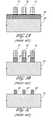
- photolithographyis first used to form a pattern of lines 10 in a photoresist layer overlying a layer 20 of an expendable material and a substrate 30 .
- the layers shown in FIG. 1are all shown schematically in cross-section.
- the patternis then transferred by an etch step (preferably anisotropic) to the layer 20 , forming placeholders, or mandrels, 40 . If the etch is anisotropic, the mandrels have approximately vertical sides, as shown.
- the photoresist lines 10can be stripped and the mandrels 40 can be isotropically etched to increase the distance between neighboring mandrels 40 , as shown in FIG. 1C .
- This isotropic etch(or shrink step) can alternatively be performed on the resist prior to transfer.
- a layer 50 of spacer materialis subsequently deposited over the mandrels 40 , as shown in FIG. 1D .
- Spacers 60i.e., material extending or originally formed extending from sidewalls of another material, are then formed on the sides of the mandrels 40 by preferentially etching the spacer material from the horizontal surfaces 70 and 80 in a directional (or anisotropic) spacer etch. Such spacers are shown in FIG. 1E .
- the remaining mandrels 40are then removed, leaving behind only the spacers 60 above substrate 30 .
- the spacers 60together act as a mask for patterning, as shown in FIG. 1F .
- pitch multiplicationincreases the density of features by reducing pitch. Pitch thus has at least two meanings: the linear spacing between identical features in a repeating pattern; and the density or number of features per linear distance. The conventional terminology is retained herein.
- the critical dimension (CD) of a mask scheme or circuit designis the scheme's minimum feature dimension, or the measurement of the smallest width of the smallest feature that exists in that design or scheme. Due to factors such as geometric complexity and different requirements for critical dimensions in different parts of an integrated circuit, typically not all features of the integrated circuit will be pitch multiplied. Furthermore, pitch multiplication entails many additional steps relative to conventional lithography; the additional steps can involve considerable additional expense. Pitch multiplication often provides less control over the resulting features than that provided by direct patterning without pitch multiplication, because the spacer pattern merely follows the outlines of the directly patterned features. Thus, pitch multiplication is typically thought useful only for regularly spaced lines, such as conductive lines for a memory array.
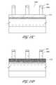
- a method of planarizing a structure in a partially fabricated integrated circuitcan comprise providing elevated features in a first region, the elevated features having spaces among them.
- the methodcan also comprise depositing a filler layer over the first region and an adjacent second region.
- the methodcan also comprise providing a protective layer over the filler layer, the protective layer being thinner over the first region compared to the second region.
- the methodcan comprise planarizing the filler layer after providing the protective layer.
- this applicationdiscloses a method of forming an array for an integrated circuit.
- the methodcan include forming pitch-multiplied features separated by spaces in a first region.
- the methodcan further include introducing a filler layer that fills the spaces and covers the pitch-multiplied features in the first region and covers the surface of a second region.
- the methodcan further include coating the filler layer with a protective layer in both the first and second regions.
- the methodcan include removing a portion of the protective layer in the first region and allowing a portion of the protective layer to remain covering the filler layer in the second region.
- the methodcan include removing portions of filler layer through planarization of the first region while the filler layer is still protected by the protective layer in the second region.
- the methodcan include removing the protective layer and planarizing the first and second regions to the same plane and forming a mask over at least one of the first and second regions.
- a method of manufacturing computer memorycan comprise: forming separated features in a memory array region; depositing a filler layer around and over the features in the memory array region and in a peripheral region such that the surface of the filler layer is less smooth than the surface of the peripheral region; forming a protective layer over the filler layer in both the memory array region and the peripheral region; exposing the filler layer under the protective layer in the array region before exposing the filler layer under the protective layer in the peripheral region; and reducing the height of the features and filler layer in the memory array region to approximately the same height as the filler layer in the peripheral region.
- FIGS. 1A-1Fare schematic, cross-sectional side views of mask lines, formed in accordance with a prior art pitch-multiplication method as described above.
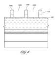
- FIG. 2is a schematic, cross-sectional side view of masking and substrate layers used to form an integrated circuit.
- FIG. 3shows the structure of FIG. 2 after photolithographic patterning of a first resist layer.
- FIG. 4shows the structure of FIG. 3 after an etch has reduced the size of the features in the pattern of FIG. 3 .
- FIG. 5shows a schematic, cross-sectional side view of masking and substrate layers used to form an integrated circuit after the pattern of FIG. 4 has been extended into underlying layers.
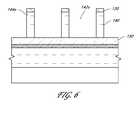
- FIG. 6shows the structure of FIG. 5 after overlying layers have been stripped.
- FIG. 7shows the structure of FIG. 6 after blanket deposition of a spacer material.
- FIG. 8shows the structure of FIG. 7 after a spacer etch and subsequent etch, leaving a pattern of free-standing spacers that has been extended into an underlying layer.
- FIG. 9shows the structure of FIG. 8 after blanket deposition of a filler material.
- FIG. 9.1shows a cross-sectional view at the edge of an array of features similar to the structure of FIG. 8 , after the spacers have been removed.
- FIG. 9.2shows the structure of FIG. 9.1 after blanket deposition of a filler material.
- FIG. 9.3shows the structure of FIG. 9.2 after deposition of a protective layer.
- FIG. 9.4shows the structure of FIG. 9.3 after a selective etch has removed portions of the protective layer and filler material.
- FIG. 9.5illustrates the structure of FIG. 9.4 during the process of another selective etch, which has begun to remove some materials but while the protective layer is still functioning to protect some of the filler material.
- FIG. 9.6illustrates the structure of FIG. 9.4 after selective etch of FIG. 9.5 is completed, the protective layer has been completely removed, and planarization achieved.
- FIGS. 9 . 7 . 2 A-Bshow scanning electron micrographs (SEMs) of an exemplary embodiment of a portion of the structure schematically depicted in FIG. 9.2 .
- FIGS. 9 . 7 . 3 A- 9 . 7 . 3 Dshow scanning electron micrographs (SEMs) of an exemplary embodiment of the structure schematically depicted in FIG. 9.3 .
- FIGS. 9 . 7 . 6 A-Cshow scanning electron micrographs (SEMs) of an exemplary embodiment of the structure schematically depicted in FIG. 9.6 , after planarization has occurred.
- the A figure(e.g., FIG. 10A ) shows a schematic plan view of the surface.
- the B figure(e.g., FIG. 10B ) shows a schematic, cross-sectional side view taken along lines B-B (e.g., 10 B- 10 B) of the A figure (e.g., FIG. 10A ).
- the C figure(e.g., FIG. 10C ) shows a schematic, cross-sectional side view taken along lines C-C (e.g., 10 C- 10 C) of the A figure (e.g., FIG. 3A ).
- the D figure(e.g., FIG., FIG.
- FIG. 10Dshows a schematic, cross-sectional side view taken along lines D-D (e.g., 10 D- 10 D) of the A figure (e.g., FIG. 10A ).
- FIGS. 18E and 22Eare similar to this pattern, showing a cross section taken along line E-E as indicated.
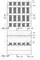
- FIGS. 10A-10Dshow the structure of FIG. 9 after a CMP process or dry etch has removed the spacers and excess filler material.
- FIGS. 11A-11Dshow the structure of FIG. 10 after deposition of multiple new layers.
- FIGS. 12A-12Dshow the structure of FIG. 11 after photolithographic patterning of a second resist layer.
- FIGS. 13A-13Dshow the structure of FIG. 12 after an etch has reduced the size of the features in the pattern of FIG. 12 .
- FIGS. 14A-14Dshow the structure of FIG. 13 after the pattern of the features of FIGS. 13A-13D has been extended into underlying layers to partially expose the crossing underlying pattern.
- FIGS. 15A-15Dshow the structure of FIG. 14 after overlying layers have been stripped.
- FIGS. 16A-16Dshow the structure of FIG. 15 after blanket deposition of a spacer material.
- FIGS. 17A-17Dshow the structure of FIG. 16 after a spacer etch and subsequent etch (that has removed the mandrels), leaving a pattern of free-standing spacers that are orthogonal to the underlying pattern.
- FIGS. 18-20illustrate a process flow that can be used in conjunction with the structure of FIG. 17 to create a mask grid with small holes that are densely spaced in an advantageous manner.
- FIGS. 18A-18Eshow the structure of FIG. 17 after an etch (e.g., a silicon dioxide etch) has removed portions of several exposed layers, while leaving intact one of the stripe materials of exposed portions of the underlying pattern.
- an etche.g., a silicon dioxide etch
- FIGS. 19A-19Dshow the structure of FIG. 18 after extending the pattern of two overlying layers into an underlying mask or temporary layer, forming holes in the underlying layer.
- the underlying temporary layeris amorphous carbon.
- FIGS. 20A-20Dshow the structure of FIG. 19 after overlying layers have been stripped to leave a pattern of holes in the lower temporary or mask (e.g., amorphous carbon) layer.
- the lower temporary or maske.g., amorphous carbon
- FIG. 21Ashows the structure of FIG. 20C after the pattern of holes in the third temporary layer has been extended into the substrate, the third temporary layer has been removed, and the holes have been filled with conductive material.
- FIG. 21Bshows the structure of FIG. 21A after the overflow conductive material has been etched away.
- FIGS. 22-25illustrate a process flow that can be used in conjunction with the structure of FIG. 17 to create small mask pillars that are densely packed in an advantageous manner.
- FIGS. 22A-22Eshow the structure of FIG. 17 after an etch (e.g., an amorphous silicon etch) to remove one of the stripe materials of exposed portions of the underlying pattern.
- an etche.g., an amorphous silicon etch
- FIGS. 23A-23Bshow the structure of FIG. 22 after a selective etch, (e.g., a silicon dioxide etch) has etched down portions of exposed materials in FIG. 22 to expose portions of an underlying mask or temporary layer.
- a selective etche.g., a silicon dioxide etch
- the underlying temporary layeris amorphous carbon.
- the selective etchhas not removed islands of one of the stripe materials (e.g., silicon) that remain in place over the temporary layer.
- FIG. 23Ashows a schematic plan view of the surface.
- FIG. 23Bshows a schematic cross-sectional side view taken along lines 23 B- 23 B of FIG. 23A .
- FIGS. 24A-24Bshow the structure of FIG. 23 after etching the exposed portions of the underlying temporary layer.
- the island patternhas thus been extended into the underlying material, leaving standing pillars or posts protected by silicon caps.
- FIGS. 25A-25Bshow the structure of FIG. 24 after a silicon etch has removed the silicon caps from the pillars or posts.
- the pillarscan be used as a mask for an underlying material.
- a partially formed integrated circuit 100is provided.
- a substrate 110is provided below various masking layers 120 - 170 .
- the layers 120 - 170can be etched to form masks for patterning underlying layers or substrate 110 .
- These maskscan be used to form various features, as discussed below.
- the featurescan comprise portions of any of the following: one or multiple transistors, diodes, capacitors, conductive lines, gates, sources, drains, or contacts to any of the above. These components can comprise portions of DRAM or flash memory arrays, NOR logic arrays, NAND logic arrays, etc.
- the featuresare formed from a substrate material that comprises a semi-conducting material.
- the semi-conducting materialcan be silicon, silicon-germanium compounds, or III-V materials.
- the term “substrate”can refer not only to the substrate layer 110 , but also to any layer that underlies another layer.
- the term “substrate”can also describe a layer or layers that have features or structures formed within them as a result of a semiconductor process (e.g., etching, doping, depositing, etc.) controlled by overlying masking layers.
- the term “pattern”can refer to an array or series of shapes that would be visible on a surface if viewed from above.
- a patterncan refer to the ensemble of shapes that correspond to a cross-section or shadow of features formed in one or multiple layers. The pattern is generally not the features themselves, but rather the design corresponding to the sizes and arrangement of the features.
- a patterncan be defined by a combination of patterns derived from multiple overlying or side by side layers.
- a patterncan originate in one layer, such as a photodefinable layer, and then be transferred to another layer, such as a temporary layer or a hard mask layer. The pattern is said to be transferred to lower layers even if feature sizes and spacings are altered (e.g., by the feature shrink step noted above).
- a new patterncan be defined by pitch multiplication, whereby two or more features in the second pattern replace one feature of the first pattern.
- a pattern in one layercan be derived from one or more patterns in another previous or overlying layer.
- a patterncan be said to be derived from another pattern even if the features in the resulting layer do not exactly resemble those features which gave rise to the original pattern, but rather the underlying pattern generally follows the outline of the overlying pattern with minor deviations in dimensions.
- the term “to pattern”can also be used as a verb and means to create or form a pattern.
- An arrangement of features formed in a particular layercan give rise to a pattern.
- An arraycan also give rise to a pattern.
- An arrayis a collection of electrical components or features, formed in a repeating configuration, that can span multiple layers of an integrated circuit. As described above, multiple cells can form a memory array for a DRAM or NAND flash memory circuit, for example, or a logic array.
- the materials for the layers 120 - 170 overlying the substrate 110are preferably chosen based upon consideration of the chemistry and process conditions for the various pattern forming and pattern transferring steps discussed herein. Because the layers between a topmost selectively definable layer 120 —which preferably is definable by a lithographic process—and the substrate 110 will preferably function to transfer a pattern derived from the selectively definable layer 120 to the substrate 110 , the layers between the selectively definable layer 120 and the substrate 110 are preferably chosen so that they can be selectively etched relative to other exposed materials. A material is considered selectively, or preferentially, etched when the etch rate for that material is at least about two times greater, preferably about ten times greater and, most preferably, at least about forty times greater than that for surrounding materials.
- the selectively definable layer 120overlies a first hard mask, or etch stop, layer 130 , which overlies a first temporary layer 140 , which overlies a second temporary layer 150 , which overlies a second hard mask, or etch stop, layer 160 , which overlies a third temporary layer 170 to be processed (e.g. etched) through a mask, which overlies the substrate layer 110 .
- the third temporary layer 170will serve as the ultimate mask through which etching (or other processing) will be performed.
- amorphous carbonis a preferred material for the third temporary layer because so many other materials—silicon, silicon oxide, silicon nitride, etc.—can be selectively etched without significantly harming the carbon layer.
- the substrate 110may comprise an interlevel dielectric (ILD) layer through which contacts are to be formed.
- ILDinterlevel dielectric
- both the mask and the underlying substrateare exposed to an etchant, which preferentially etches away the substrate material.
- the etchantscan also wear away the mask materials, albeit at a slower rate.
- the maskcan be worn away by the etchant before the pattern transfer is complete.
- additional mask layersmay be used to prevent the mask pattern from being worn away before the pattern transfer is complete. See FIGS. 9 . 1 - 9 . 7 for further illustration of related masking processes.
- hard mask layers 130 and 160advantageously play a protective role, protecting underlying layers from unwanted degradation during etching of overlying layers.
- various other layerssuch as the second hard mask layer 160 itself, may be omitted and overlying mask layers may be sufficient for the desired pattern transfer.
- Higher numbers of mask layersare advantageous for transferring patterns to difficult to etch substrates, such as a substrate comprising multiple materials or multiple layers of materials, or for forming small and high aspect ratio features.
- the selectively definable layer 120is preferably formed of a photoresist, including any photoresist known in the art.
- the photoresistcan be any photoresist compatible with 13.7 nanometer (nm), 157 nm, 193 nm, 248 nm or 365 nm wavelength systems, 193 nm wavelength immersion systems or electron beam lithographic systems.
- photoresist materialsinclude argon fluoride (ArF) sensitive photoresist, i.e., photoresist suitable for use with an ArF light source, and krypton fluoride (KrF) sensitive photoresist, i.e., photoresist suitable for use with a KrF light source.
- ArF photoresistsare preferably used with photolithography systems utilizing relatively short wavelength light, e.g. 193 nm.
- KrF photoresistsare preferably used with longer wavelength photolithography systems, such as 248 nm systems.
- the layer 120 and any subsequent resist layerscan be formed of a resist that can be patterned by nano-imprint lithography, e.g. by using a mold or mechanical force to pattern the resist.
- Photoresistis typically patterned by being exposed to radiation through a reticle and then developed.
- radiatione.g. light
- the radiationactivates a photosensitive compound, e.g., a photo-induced acid generator (PAG), which decreases the solubility of the photoresist, e.g., by causing it to polymerize.
- PAGphoto-induced acid generator
- Preferred embodimentsmay be applied using any definable material, including positive or negative photoresist.
- a preferred reticle used in testing of some embodimentsis T37Z 46/47 reticle.
- the material for the first hard mask layer 130preferably comprises an inorganic material, and exemplary materials include silicon dioxide (SiO 2 ), silicon, or a dielectric anti-reflective coating (DARC), such as a silicon-rich silicon oxynitride.
- the first hard mask layer 130is a dielectric anti-reflective coating (DARC).
- DARCdielectric anti-reflective coating
- hard mask layer 130can serve both as an intermediate hard mask and to reduce reflections during lithography.
- DARC material for the first hard mask layer 130can be particularly advantageous for forming patterns having pitches near the resolution limits of a photolithographic technique.
- the DARCcan enhance resolution by minimizing light reflections, thus increasing the precision with which photolithography can define the edges of a pattern.
- an organic bottom anti-reflective coating (BARC)(not shown) can similarly be used in addition to or in place of the first hard mask layer 130 to control light reflections.
- the first temporary layer 140is preferably formed of amorphous carbon, which offers very high etch selectivity relative to the preferred hard mask materials. More preferably, the amorphous carbon is a form of transparent carbon that is highly transparent to light and which offers further improvements for photo alignment by being transparent to wavelengths of light used for such alignment. Deposition techniques for forming a highly transparent carbon can be found in A. Helmbold, D. Meissner, Thin Solid Films, 283 (1996) 196-203, the entire disclosure of which is incorporated herein by reference and made part of this specification.
- the second temporary layer 150is preferably formed of amorphous silicon.
- amorphous siliconcan be selectively etched while other adjacent materials (such as oxide layers) remain intact.
- the second hard mask, or etch stop layer 160preferably comprises silicon dioxide (SiO 2 ), silicon, or a dielectric anti-reflective coating (DARC), such as a silicon-rich silicon oxynitride, or aluminum oxide (Al 2 O 3 ).
- the first hard mask layer 160is a DARC.
- the third temporary layer 170is preferably formed of amorphous carbon, which has excellent etch selectivity relative to many materials. Benefits of amorphous carbon are further discussed above with respect to the first temporary layer 140 .
- the substratecan be a silicon wafer used for formation of integrated circuits.
- Various substrate materialscan be used.
- the thicknesses of the layers 120 - 170are preferably chosen depending upon compatibility with the etch chemistries and process conditions described herein. For example, when transferring a pattern from an overlying layer to an underlying layer by selectively etching the underlying layer, materials from both layers are removed to some degree.
- the upper layeris preferably thick enough so that it is not worn away over the course of the pattern transfer.
- the hard mask layersare advantageously thin so that their transfer or removal can occur quickly, exposing surrounding materials to less wear.
- the selectively definable layer 120is a photodefinable layer preferably between about 100-250 nm thick and, more preferably, between about 130-200 nm thick.
- the first hard mask layer 130e.g., SiO 2 or DARC
- the first temporary layer 140e.g., amorphous carbon
- the second temporary layer 150(e.g., amorphous silicon) is preferably between about 30-50 nm thick and, more preferably, between about 35-45 nm thick.
- the second hard mask layer 160(e.g., SiO 2 or DARC) is preferably between about 10-30 nm thick and, more preferably, about 15 nm thick.
- the third temporary layer 170(e.g., amorphous carbon) is preferably between about 100-300 nm thick and, more preferably, between about 150-250 nm thick.
- various layers discussed hereincan be formed by various methods known to those of skill in the art.
- various vapor deposition processessuch as chemical vapor deposition
- a low temperature chemical vapor deposition processis used to deposit the hard mask layers or any other materials, e.g. spacer material, over carbon.
- Such low temperature deposition processesadvantageously prevent chemical or physical disruption of the underlying amorphous carbon layer.
- Spin-on-coating processescan be used to form photodefinable layers.
- amorphous carbon layerscan be formed by chemical vapor deposition using a hydrocarbon compound, or mixtures of such compounds, as carbon precursors.
- Exemplary precursorsinclude propylene, propyne, propane, butane, butylene, butadiene and acetylene.
- a suitable method for forming amorphous carbon layersis described in U.S. Pat. No. 6,573,030 B1, issued to Fairbairn et al. on Jun. 3, 2003, the entire disclosure of which is incorporated herein by reference and made part of this specification.
- the amorphous carbonmay be doped.
- a suitable method for forming doped amorphous carbonis described in U.S. patent application Ser. No. 10/652,174 to Yin et al., the entire disclosure of which is incorporated herein by reference and made part of this specification.
- a pattern of spacersis formed by pitch multiplication and used to create an underlying striped structure (see FIG. 10 ) for subsequent method steps.
- One example of an etch sequence for this phaseis the following: 1) deposition of multiple layers; 2) photolithographic patterning of a first layer; 3) shrinking of features; 4) extension of pattern into underlying layers; 5) removal of remaining portions of overlying layers; 6) blanket deposition of spacer material; 7) spacer etch; 8) removal of spacer mandrels; 9) extension of spacer pattern into underlying material; 10) blanket deposition of a filler material; 11) removal of spacers; and 12) planarization using protective masking techniques.
- a pattern comprising gaps or spaces 122 delimited by definable material features 124is formed in the definable layer 120 .
- the spaces 122can be formed by, e.g., photolithography, in which the selectively definable layer 120 is exposed to radiation through a reticle and then developed. After being developed, the remaining definable material, photoresist in the illustrated embodiment, forms mask features such as the illustrated lines 124 (shown in cross-section).
- the pitch of the lines 124is equal to the sum of the width of a line 124 and the width of a neighboring space 122 .
- the pitchis preferably at or near the limits of the photolithographic technique used to pattern the definable layer 120 .
- the pitch of the lines 124can be about 200 nm.
- the pitchmay be at the minimum pitch of the photolithographic technique and the spacer pattern discussed below can advantageously have a pitch below the minimum pitch of the photolithographic technique.
- a preliminary stepcan comprise creating a series of photoresist lines 124 .
- photolithographycan be used to form a plurality of lines in a mask material.
- Conventional photolithographycan form lines having a pitch no smaller than that definable by photons.
- subsequent pitch multiplicationcan form lines having a pitch that is smaller than that definable by conventional photolithography.
- FIG. 4shows the structure of FIG. 3 after the lines 124 have been shrunk by an isotropic etch to create modified lines 124 a .
- the spaces 122can optionally be widened or narrowed to a desired dimension. For example, as illustrated in FIG. 6 , the spaces 122 have been widened by etching the photoresist lines 124 , to form modified spaces 122 a and modified lines 124 a .
- the photoresist lines 124are preferably reduced in size using an isotropic etch, such as a sulfur oxide plasma, e.g., a plasma comprising SO 2 , O 2 , N 2 and Ar, or any other suitable plasma.
- a sulfur oxide plasmae.g., a plasma comprising SO 2 , O 2 , N 2 and Ar, or any other suitable plasma.
- Two other plasmas that can be usedare an HBr/O 2 plasma or a Cl 2 /O 2 plasma.
- the isotropic etchdegrades the exposed surfaces from all directions.
- the corners of lines 124 ahave been depicted as slightly rounded in FIG. 4 .
- the extent of the etchis preferably selected so that the widths of the lines 124 a are substantially equal to the desired spacing between the later-formed spacers 182 , as will be appreciated from the discussion of FIGS. 7-8 .
- this etchallows the lines 124 a to be narrower than would otherwise be possible using the photolithographic technique used to pattern the photodefinable layer 120 .
- this etchcan reduce their size even further, taking them below that resolution limit.
- the etchcan smooth the edges of the lines 124 a , thus improving the uniformity of those lines.
- the spaces 122 a between the lines 124 acan be narrowed by expanding the lines 124 to a desired size.
- additional material(not shown) can be deposited over the lines 124 , or the lines 124 can be chemically reacted to form a material (not shown) having a larger volume to increase their size.
- the modified lines 124 adefine the dimensions of placeholders or mandrels along which a pattern of spacers 182 ( FIG. 8 ) will be formed after transfer of the pattern to an underlying layer ( FIGS. 5 and 6 ) and blanket deposition of a spacer material 180 ( FIG. 7 ).
- the temporary layer 140can be omitted and the spacer material can be deposited directly on the photo-defined lines 124 or the thinner lines 124 a.
- the pattern of the lines 124can be transferred to underlying layers without first being trimmed or having their width's reduced as described above.
- a pattern corresponding to that of lines 124can be formed in the temporary layer 140 and the features of that pattern can be reduced in width with a shrink step.
- the pattern in the photodefinable layer 120is preferably transferred to the first temporary layer 140 to allow for later deposition of a layer 180 of spacer material ( FIG. 7 ).
- the temporary layer 140is preferably formed of a material that can withstand the process conditions for spacer material deposition and etch, discussed below.
- the material forming the temporary layer 140preferably has a higher heat resistance than photoresist and is preferably selected such that it can be selectively removed relative to the material for the spacers 182 ( FIG. 8 ) and the underlying layer 150 .
- the layer 140is preferably formed of amorphous carbon.
- the pattern of lines 124 a and spaces 122 a in FIG. 4can be extended into, or transferred to underlying layers. This pattern extension can be accomplished by selectively etching the materials that form layers 130 and 140 , while lines 124 a form a protective mask that prevents the etchant from removing the material located underneath lines 124 a.
- an anisotropic etchcan be used, such as an etch using a fluorocarbon plasma.
- a wet (isotropic) etchmay also be suitable if the hard mask layer 130 is thin.
- Preferred fluorocarbon plasma etch chemistriesinclude CF 4 , CFH 3 , CF 2 H 2 and CF 3 H for etching the preferred DARC material.
- an SO 2 -containing plasmae.g. a plasma containing SO 2 , O 2 and Ar
- the SO 2 -containing plasmacan etch carbon of the preferred temporary layer 140 at a rate greater than 20 times and, more preferably, greater than 40 times the rate that the hard mask layer 130 is etched.
- a suitable SO 2 -containing plasmais described in U.S. patent application Ser. No. 10/931,772 to Abatchev et al., filed Aug. 31, 2004, entitled Critical Dimension Control, the entire disclosure of which is incorporated herein by reference and made part of this specification.
- FIG. 5shows lines 124 a intact after the pattern has been extended into the first temporary layer 140
- the SO 2 -containing plasmacan simultaneously etch the temporary layer 140 and also remove the remaining portion of definable layer 120 .
- the remaining portions of the layer 120can be stripped away using a selective etch.
- the remaining portions of 120can be etched away during an amorphous carbon etch step such as the step that extends the pattern down into the layer 140 .
- the line pattern originally formed in the definable layer 120has been transferred to the hard mask and temporary layers 130 and 140 .
- the transferred patternis approximately the same as the line pattern originally formed in layer 120 ; the transferred pattern has lines 144 a and spaces 142 a that generally correspond to lines 124 a and spaces 122 a , respectively.
- portions of the hard mask layer 130remain in place as protective caps on the lines 144 a . These portions of the layer 130 can act as etch stops in subsequent steps.
- a patternis formed in an overlying layer and later transferred to an underlying layer.
- the illustrated walls of the features formed in layers 130 and 140are vertical, where these layers have been etched.
- directional or anisotropic etchescan be used.
- etching processescan alter the precision with which a pattern in an overlying layer corresponds to a pattern created in an underlying layer.
- pattern transfer from layer to layeris generally illustrated schematically to be a precise process, with vertical walls, such precision may be difficult to achieve in practice.
- pattern transferis intended to encompass general correspondence between underlying and overlying patterns.
- pattern transferis meant to encompass modification of the features originally defining the pattern—for example by enlarging or shrinking those features—where such modification does not change the pitch.
- a layer 180 of spacer materialis preferably blanket deposited so that it conforms to the exposed surfaces, including the second temporary layer 150 and the lines 144 a .
- portions of the hard mask layer 130can be left in place—to subsequently act as CMP etch stops—on top of lines 144 a when the layer 180 of spacer material is deposited.
- the hard mask portionscan be removed with a selective etch before spacer deposition.
- the spacer materialcan be any material that can act as a mask for transferring a pattern to underlying layers, or that otherwise can allow processing of underlying structures through the mask being formed.
- the spacer materialpreferably: 1) can be deposited with good step coverage; 2) can be deposited at a temperature compatible with the temporary layer 140 and underlying layers; and 3) can be selectively etched relative to the temporary layer 140 and any layer directly underlying the temporary layer 140 .
- Preferred materialsinclude silicon oxides and nitrides.
- the spacer materialis preferably deposited by chemical vapor deposition or atomic layer deposition.
- the layer 180is preferably deposited to a thickness of between about 20-60 nm and, more preferably, about 20-50 nm.
- the step coverageis about 80% or greater and, more preferably, about 90% or greater.
- FIG. 8shows the structure of FIG. 7 after a spacer etch and subsequent etch, leaving a pattern of free-standing spacers that has been extended into an underlying layer.
- the spacer etchcan comprise an anisotropic etch to remove spacer material from horizontal surfaces.
- the spacer etchcan be performed using a fluorocarbon plasma.
- the spacer etchcan also be performed using HBr/Cl plasma for a silicon spacer material. (Note that preferred embodiments use silicon oxide spacers, however). After a spacer etch is performed, it can leave behind a pattern of elongate spacers having effectively reduced pitch relative to the lines.
- the remaining portions of hard mask layer 130 (if still present) and the temporary layer 140are next removed to leave freestanding spacers 182 .
- the remaining portions (in the form of lines 144 a ) of the first temporary layer 140are selectively removed, preferably using a sulfur-containing plasma etch such as an etch using SO 2 . In this way, features of one pattern are removed to leave behind another pattern formed by the spacers.
- pitch-reductionhas been performed using a spacer material to create masking features.
- the masking features formed in this waycan have a smaller pitch than the photoresist lines and can comprise pitch-reduced masking lines separated by pitch-reduced spaces; pitch multiplication has been accomplished.
- the pitch of the pattern formed by spacers 182is roughly half that of the pattern formed by photoresist lines 124 a and spaces 122 a ( FIGS. 3-5 ), where the pitch was originally determined by photolithography.
- a spacer pattern having a pitch of about 100 nmcan be formed.
- the pattern formed by the spacers 182can be extended into the underlying second temporary layer 150 .
- the extensioncan be accomplished with a selective etch chemistry.
- a selective etch chemistryFor example, if the spacers 182 are formed from silicon dioxide and the underlying layer 150 is formed from amorphous silicon, an etch can remove the latter while leaving the former largely intact.
- a preferred etchincludes a physical component and preferably can also include a chemical component and can be, e.g. a reactive ion etch (RIE), such as an HBr/Cl 2 etch.
- RIEreactive ion etch
- Such an etchcan be performed, for example, using a LAM TCP9400 (available commercially from LAM Research Corporation of Fremont, Calif.) flowing about 0-50 sccm Cl 2 and about 0-200 sccm HBr at about 7-60 mTorr pressure with about 300-1000 W top power and about 50-250 W bottom power.
- LAM TCP9400available commercially from LAM Research Corporation of Fremont, Calif.
- FIG. 9shows the structure of FIG. 8 after blanket deposition of a filler material 190 .
- the filler material 190is advantageously formed from silicon dioxide (SiO 2 ).
- the spacers 182 and the filler material 190are formed from the same or similar materials, as will be better understood from the discussion of FIGS. 17-20 , and 22 - 23 below.
- the spacers 182 and the filler material 190can both be formed from silicon dioxide.
- One preferred process for depositing the filler material 190i.e., silicon dioxide
- Applied Materials' Producer® HARPTM system.(HARP stands for “High Aspect Ratio Process.”)
- the spacers 182can be removed before the filler material 190 is deposited.
- a wet etchcan be used to remove the spacers if the hard mask layer 160 is formed from a DARC material. Removal of the spacers 182 can allow good coverage by the filler material 190 .
- some embodimentscomprise a planarization step.
- planarization of two different regions with different heightscan be difficult. For example, etch processes tend to planarize uneven surfaces simultaneously. That is, two surfaces of different heights will both be worn down by an etch, not just the higher surface.
- FIGS. 8-9show cross sections of the structure formed in the middle of the array of patterned features.
- the edge of the arrayis schematically depicted in FIGS. 9 . 1 - 9 . 6 , which illustrate a planarization process that uses a protective layer.
- FIG. 9.1shows the edge of the array at a similar point in the process as depicted in FIG. 8 , (after the pattern formed by the spacers 182 is extended into the underlying second temporary layer 150 ), except that the spacers 182 have been removed.
- the spacersare not removed and subsequent steps can be performed with the spacers 182 in place, until they are removed during planarization.
- FIG. 9.2shows the structure of FIG. 9.1 after blanket deposition of a filler material 190 .
- the filler materialhas a slightly non-planar, undulating surface in a higher region 912 with hills that roughly overlie the features (remaining portions of the temporary layer 150 ) and valleys that roughly overlie the spaces between the features.
- the higher region 912can have underlying features that have been pitch-multiplied, causing the features to be tightly crowded together with relatively small spaces in between.
- the featurescan be spacers 182 or the remaining portions of the temporary layer 150 .
- the valleys overlying the spaces between featuresare generally less deep and, for some purposes, the higher region 912 (with the filler material 190 deposited thereon) can be effectively treated as a monolithic higher region 912 rather than a series of discrete features.
- etch processesincluding dry etch-back processes and chemical mechanical planarization (CMP) processes can be used.
- Some etch processesinvolve only chemical etching or ion bombardment; CMP processes include both a chemical aspect and a mechanical aspect, each of which contributes to removing some of the surface material.
- the mechanical aspect of a CMP processcan be rotating pads that physically wear down a surface like a rotating sander. However, these processes tend to planarize uneven surfaces simultaneously. That is, two surfaces of difference heights will both be worn down by an etch, not just the higher surface.
- FIG. 9.3shows the structure of FIG. 9.2 after blanket deposition of a protective layer 920 .
- the protective layer 920is thinner where it overlies the higher region 912 and thicker where it overlies the lower region 914 .
- the protective layer 920can be a spin-on film (e.g. photoresist, BARC, organic under layer, or SOD).
- the protective layer 920is formed from a material for which an etch chemistry will selectively etch the filler material 190 more quickly than the protective layer 920 .
- the thickness of the protective layer 920 over the higher region 912 and lower region 914can be determined by the viscosity of the protective layer 920 , by the roughness or flatness of the underlying surface, and by the method of deposition. Spin-on coating can cause the undulating higher region 912 to have a thinner protective layer 920 than the lower, flatter region 914 , as shown.
- the thickness of the protective layer 920 in the higher region 912can be approximately 24 nm, while the thickness of the protective layer 920 in the lower region 914 can be approximately 63 nm.
- the higher region 912is less rough and undulating than that depicted in FIGS. 9.2 and 9 . 3 .
- the thinner coating of the protective material 920 on the higher region 912is due to the spin-on process, which generally tends to cause material to flow to the lowest point on the structure.
- the protective layer 920is thicker over the lower region 914 than the higher region 912 .
- the protective layers over the higher region 912 and the lower region 914are approximately planar on the top surface so that the two regions 912 and 914 have the same height when the protective layer is applied.
- FIG. 9.4illustrates the structure of FIG. 9.3 after a first etch step.
- a two-step etchcan be used to planarize the structure depicted in FIG. 9.3 .
- a first etch stepcan have a selectivity that etches the protective layer 920 more rapidly than the filler material 190 . This step can remove the portion of the protective layer 920 that overlies the higher region 912 , as well as removing some of the filler material 190 . This step can also remove some (but not all) of the protective layer 920 that overlies the lower region 914 .
- the protective layer 920is photoresist and the filler material 190 is oxide, a dry etch chemistry can be used for the first etch step. In some embodiments, reactive ion etches and/or CMP processes can also be used.
- FIG. 9.5illustrates the structure of FIG. 9.4 at an intermediate time during the second etch step, after some materials have been removed but while the protective layer 920 is still functioning to protect the filler material 190 in the lower region 914 .
- a second etch stepcan have a selectivity that etches the filler material 190 more rapidly than the protective layer 920 and that etches the filler material 190 at approximately the same rate as the second temporary layer 150 .
- this second stepcan remove some of the filler material 190 , reducing the height of the higher region 912 with respect to the lower region 914 .
- the protective layer 920can also be partly removed during this step. If the protective layer 920 is photoresist and the filler material 190 is oxide, a fluorocarbon etch can be used for the second etch step.
- FIG. 9.6illustrates the structure of FIG. 9.4 after the second etch step is completed, the protective layer 920 has been completely removed, and planarization achieved.
- the second etch stepcan continue until the protective layer 920 is completely removed.
- the last part of the protective layer 920is removed at the same time that the higher region 912 and the lower region 914 have been etched to approximately the same height.
- the array and the regions surrounding the arrayhave been planarized without having to over-etch and waste time and materials.
- the second temporary layer 150 and the filler material 190preferably are etched at approximately the same rate so that the planar surface is maintained.
- the filler material 190is thicker than the remaining portions of the temporary layer 150 , so the protective layer 920 is completely removed before any of the temporary layer 150 is exposed.
- the etchcan continue to remove the intervening filler material (which is inherently etched at a uniform rate because it is the same material both above the array features in what was formerly the higher region 912 and in the lower region 914 ).
- a separate (third) etchcan be performed to further smooth or clean the planarized surface.
- the third etch stepcan be a CMP process for example.
- FIGS. 9 . 7 . 2 A and 9 . 7 . 2 Bshow scanning electron micrographs (SEMs) of an exemplary embodiment of a portion of the structure schematically depicted in FIG. 9.2 .
- the edge of the arrayis not visible in these views, which show only the higher region 912 .
- FIGS. 9 . 7 . 3 A- 9 . 7 . 3 Dshow scanning electron micrographs (SEMs) of an exemplary embodiment of the structure schematically depicted in FIG. 9.3 .
- SEMsscanning electron micrographs
- FIGS. 9 . 7 . 6 A, 9 . 7 . 6 B and 9 . 7 . 6 Cshow scanning electron micrographs (SEMs) of an exemplary embodiment of the structure schematically depicted in FIG. 9.6 , after planarization has occurred.
- FIGS. 9 . 7 . 2 A- 9 . 7 . 6 Cshow structure that was formed using a LAM TCP9400 device with the following etch parameters:
- a protective coatingcan protect a lower surface while a higher surface is exposed and etched by an etch process. If the higher surface wears down more slowly than the protective coating and if sufficient topography is still remaining on the lower surface, the protective coating can be re-applied. If the etch has a mechanical component and the protective coating is thick enough, a surface that is higher than the lower surface will be exposed first from the protective coating, so the higher surface will be etched for at least a short time without the lower surface being etched.
- two layerscan be deposited: a first layer (e.g., the filler material 190 ) that fills in the space in between the features of the array and a second layer (e.g., the protective layer 920 ) that protects portions of the first layer.
- the second layersmooths over and fills in the depressions or shorter areas still present after deposition of the first layer.
- the second layeris a protective sacrificial layer because it is ultimately removed.
- the first layeris also partly removed, but portions of that layer remain interspersed with the features of the array after planarization.
- the pattern of the spacers 182has not been extended or transferred into an underlying layer, so the features of the array are the spacers 182 themselves. In this case, the first layer can fill in the space between the spacers 182 .
- planarization processes disclosed hereincan be used in a variety of circumstances, and not just in the context of the pitch-doubling and masking steps described in detail herein.
- the disclosed planarization processcan be used when a region having features (e.g., a memory array) is located next to a region without features (e.g., a peripheral or logic region). If the features are taller than the surface of the featureless region, their heights can be reduced using the techniques discussed herein.
- the planarization processcan be used where a higher surface having relatively non-smooth topography is located next to a lower surface, allowing a protective layer to be thinner on the higher surface than on the lower surface.
- FIGS. 10-20 and 22 - 23each illustrate at least four corresponding views, lettered A-D as follows: 10 A- 10 D, 11 A- 11 D, etc.
- the views designated with an “A”consistently show a top or plan view, where hatching has been included for convenience.
- the views B-Cconsistently show cross sections of the same structure depicted in the corresponding figure A.
- those views designated with a “B”consistently show the structure in the same orientation as other views designated with a “B.”
- the orientationsare also similar for “C” designations, and likewise for “D” designations.
- FIGS. 10A-10Dshow the structure of FIG. 9 after removal of the spacers 182 and a portion of the filler material 190 , through, for example, a chemical mechanical polishing (CMP) process.
- CMPchemical mechanical polishing
- a dry etch or a plasma etchcan also be used for planarization.
- a thin etch stop layeris preferably added between the hard mask layer 160 and the temporary layer 150 .
- the etch stop layercan be formed from Si 3 N 4 , for example.
- FIG. 10Ashows a schematic plan view of the surface after the planarization.
- the surfaceexhibits a striped pattern with alternating stripes of the filler material 212 , which is amorphous silicon, for example, and the stripes 214 , which can be silicon dioxide, for example.
- the stripes 212 of amorphous siliconhave been formed in the second temporary layer 150 and the stripes 214 of silicon dioxide are the remaining portions of the filler material 190 that fill the spaces between the stripes 212 .
- the surface in FIG. 10Ais depicted with cross-hatching to show the material that comprises the striped structures.
- the stripes 212preferably have widths 213 in a range of approximately 30-70 nm.
- the stripes 214preferably have widths 215 in a range of approximately 30-70 nm. More preferably, the stripes 212 and 214 each have widths 213 and 215 , respectively, of approximately 50 nm. In the latter case, the pattern formed by the stripes has a pitch of approximately 100 nm.
- FIG. 10Bshows a schematic cross-sectional side view taken along lines 10 B- 10 B of FIG. 10A .
- This viewreveals that the two sets of stripes are formed on the same “level.”
- levelis used to designate a portion of the integrated circuit that is generally located in a thick plane that is parallel to and equidistant from the plane of the surface of the substrate 110 .
- the layer 160is located at a different level from that of layer 170 , but the stripes 212 and the stripes 214 are located at the same level.
- the term “layer”is generally used to refer to a portion of the integrated circuit formed from the same material and deposited together.
- FIG. 10Cshows a schematic, cross-sectional side view taken along lines 10 C- 10 C of FIG. 10B .
- FIG. 10Dshows a schematic, cross-sectional side view taken along lines 10 D- 10 D of FIG. 10B .
- a pattern of spacershas been formed by pitch multiplication and used to create an underlying striped structure or “first pattern” derived from and pitch multiplied relative to the pattern of the first resist mask.
- a second pattern of spacersis formed by pitch multiplication and used to create an overlying striped structure (see FIG. 17 ) that crosses the underlying striped structure of FIG. 10 .
- One example of an etch sequence for this phaseis the following: 1) deposition of multiple layers; 2) photolithographic patterning of an overlying layer; 3) shrinking of features; 4) extension of pattern into underlying layers; 5) removal of remaining portions of overlying layers; 6) blanket deposition of spacer material; 7) spacer etch; 8) removal of spacer mandrels.
- FIGS. 11A-11Dshow the structure of FIG. 10 after deposition of multiple new masking layers, 320 - 340 .
- the pattern having the stripes 212 and the stripes 214now underlies multiple new layers of material.
- layers 320 - 340can also be etched to form masks for patterning underlying layer(s) of substrate 110 .
- These maskscan be used to form various features, as discussed below.
- the featurescan comprise portions of one or multiple integrated circuit components.
- FIG. 11Ashows a schematic plan view of the surface.
- FIG. 11Bshows a schematic cross-sectional side view taken along lines 11 B- 11 B of FIG. 11A .
- FIG. 11Cshows a schematic, cross-sectional side view taken along lines 11 C- 11 C of FIG. 11B .
- FIG. 11Dshows a schematic, cross-sectional side view taken along lines 11 D- 11 D of FIG. 11B .
- masking layer 320preferably has similar properties to those described above with respect to layer 120 .
- layer 330preferably has similar properties to those described above with respect to layer 130 .
- the fourth temporary layer 340preferably has similar properties to those described above with respect to the layer 140 .
- the materials for layers 320 - 340 overlying the substrate 110are preferably chosen based upon consideration of the chemistry and process conditions for the various pattern forming and pattern transferring steps discussed herein. Such layers are also preferably chosen so that they can be selectively etched relative to other exposed materials.
- the second selectively definable layer 320overlies a third hard mask, or etch stop, layer 330 , which overlies a fourth temporary layer 340 , which overlies the level having the stripes 212 and 214 .
- a third hard mask, or etch stop, layer 330which overlies a fourth temporary layer 340 , which overlies the level having the stripes 212 and 214 .
- Underlying levels 160 and 170 , as well as substrate 110remain intact.
- one or more of the layers 320 - 340can be omitted in some embodiments.
- the second selectively definable layer 320is preferably formed of a photoresist, including any photoresist known in the art. All the preferred properties and alternatives described above with reference to the layer 120 also apply to the layer 320 .
- the third hard mask layer 330preferably comprises an inorganic material, and in the illustrated embodiment, the layer 330 is a DARC. All the preferred properties and alternatives described above with reference to the layer 130 also apply to the layer 330 .
- the fourth temporary layer 340is preferably formed of amorphous carbon. All the preferred properties and alternatives described above with reference to the layer 140 also apply to the layer 340 .
- the layer 340is formed from amorphous carbon in some embodiments. Because it is sometime difficult to achieve good step coverage of amorphous carbon deposition, the underlying striped surface has been planarized (see FIG. 10 ).
- the thicknesses of the layers 320 - 340are preferably chosen depending upon compatibility with the etch chemistries and process conditions described herein. Thus, as described above, thicknesses must allow for appropriate pattern transfer, and the hard mask layer 330 is advantageously thin so that its transfer or removal can occur quickly, exposing surrounding materials to less wear.
- the second selectively definable layer 320is a photodefinable layer preferably between about 100-250 nm thick and, more preferably, between about 130-200 nm thick.
- the third hard mask layer 330is preferably between about 10-30 nm thick and, more preferably, between about 15-25 nm thick.
- the fourth temporary layer 340is preferably between about 130-200 nm thick and, more preferably, between about 140-160 nm thick.
- the layers 320 , 330 , and 340can be formed by various methods known to those of skill in the art. For example, the methods described above for forming layers 120 , 130 , and 140 can be used to form layers 320 , 330 , and 340 , respectively.
- FIGS. 12A-12Dillustrate a pattern formed in the layer 320 , having lines 324 interspersed with spaces 322 .
- the preferred properties of and methods for forming the lines 124 described above in FIG. 3 et seq.also apply to lines 324 , however, the lines 324 are not parallel to the lines 124 . This can be seen—even though the lines 124 have been removed—by observing that the stripes 212 and the stripes 214 are not parallel to the lines 324 . Thus, because the stripes 212 and 214 are elongate in the same elongate dimension of the lines 124 , the lines 124 and the lines 324 are not parallel.
- the illustrated methodcan be said to call for applying a crossing pattern of photoresist over an underlying pattern.
- one pattern“crosses” a second pattern when an elongate dimension of the first pattern is not aligned with or parallel to an elongate dimension of the second pattern.
- the elongate dimension of the lines 124is aligned with the elongate dimension of the stripes 212 and 214 , but the elongate dimension of the stripes 212 and 214 crosses the elongate dimension of the lines 324 .
- the lines 124can be described as aligned with the stripes 212 and 214
- the stripes 212 and 214can be described as crossing the lines 324 .
- the lines 324not only cross, they cross perpendicularly the stripes 212 and 214 .
- the term “cross”is intended to include all non-parallel angles, not just a 90 degree angle.
- the exemplary features and/or holes formed by the illustrated methodshave a generally rectangular footprint (see, e.g., FIGS. 21A , 25 A, and 27 A), other footprints such as skewed quadrangle or diamond-shaped footprints are also contemplated.
- FIGS. 12A-12Dshow the structure of FIG. 11 after photolithographic patterning of an overlying resist layer.
- FIG. 12Ashows a schematic plan view of the surface.
- FIG. 12Bshows a schematic cross-sectional side view taken along lines 12 B- 12 B of FIG. 12A .
- FIG. 12Cshows a schematic, cross-sectional side view taken along lines 12 C- 12 C of FIG. 12B .
- FIG. 12Dshows a schematic, cross-sectional side view taken along the lines 12 D- 12 D of FIG. 12B .
- the pattern created by the series of photoresist lines 324has been formed through conventional photolithography.
- the shrink stepcan be accomplished to make the lines 324 thinner and spacer formation can be accomplished using the modified lines 324 a as mandrels, or the pattern can be transferred to an underlying layer before the shrink step is accomplished.
- the shrink stepis performed on photoresist lines 324 , the pattern is then transferred to an underlying layer, and portions of the underlying layer form spacer mandrels.
- FIGS. 13A-13Dshow the structure of FIG. 12 after the lines 324 have been shrunk, by an isotropic etch, for example, to create modified lines 324 a .
- the shrink stepalso widens the spaces 322 to form modified spaces 322 a .
- FIG. 13Ashows a schematic plan view of the surface.
- FIG. 13Bshows a schematic cross-sectional side view taken along lines 13 B- 13 B of FIG. 13A .
- FIG. 13Cshows a schematic, cross-sectional side view taken along lines 13 C- 13 C of FIG. 13B .
- FIG. 13Dshows a schematic, cross-sectional side view taken along lines 13 D- 13 D of FIG. 13B .
- FIGS. 13A-13Dpreferably shares many characteristics of the features described in conjunction with FIG. 4 . Similar methods to achieve that structure can also be used; preferred etch materials and methods, and desirable configurations are described above.
- the photoresist lines 324are preferably reduced in size using an isotropic etch, such as a sulfur oxide plasma, e.g. a plasma comprising SO 2 , O 2 , N 2 and Ar, or any other suitable plasma.
- a sulfur oxide plasmae.g. a plasma comprising SO 2 , O 2 , N 2 and Ar
- Two other plasmas that can be used, for example,are an HBr/O 2 plasma or a Cl 2 /O 2 plasma.
- the modified lines 324 adefine the dimensions of the placeholders or mandrels along which a pattern of spacers will be formed.
- the pattern of the lines 324can be transferred to underlying layers without first being trimmed or having their width's reduced as described above.
- a pattern corresponding to that of lines 324can be formed in the temporary layer 340 and the features of that pattern can be reduced in width with a shrink step.
- the temporary layer 340can be omitted and the spacer material can be deposited directly on the photo-defined lines 324 or the thinner lines 324 a.
- lines 324 acreate a mask for placeholders or mandrels that will later be formed in the underlying layer 340 , along which a pattern of spacers 382 ( FIG. 17 ) will be formed after blanket deposition of a spacer material 380 ( FIG. 16 ).
- FIGS. 14A-14Dillustrate how the pattern in the photodefinable layer 320 can be extended into the fourth temporary layer 340 .
- FIG. 14Ashows a schematic plan view of the surface.
- FIG. 14Bshows a schematic cross-sectional side view taken along lines 14 B- 14 B of FIG. 14A .
- FIG. 14Cshows a schematic, cross-sectional side view taken along lines 14 C- 14 C of FIG. 14B .
- FIG. 14Dshows a schematic, cross-sectional side view taken along lines 14 - 14 D of FIG. 14B .
- the fourth temporary layer 340preferably has the advantageous properties described above for the second temporary layer 140 such as high heat resistance.
- the pattern of lines 324 a and spaces 322 a in FIGS. 13A-13Dcan be extended into or transferred to underlying layers in a similar way to the way the pattern of lines 124 a and spaces 122 a was transferred to underlying layers, using, for example, a selective etch to transfer the pattern into the hard mask layer 330 and an SO 2 -containing anisotropic plasma etch to transfer the pattern into the fourth temporary layer 340 .
- Preferred and alternative etch chemistriesare described above.
- the described etch stepsremove the portions of the layers 330 and 340 that are not masked by the lines 324 a , thus leaving portions of the stripes 212 and 214 exposed.
- the surfaces visible in FIG. 14Ahave been hatched to reveal the underlying materials of the structure depicted, and to show how the lines 324 a cross the stripes 212 and 214 .
- FIGS. 15A-15Dshow the structure of FIG. 14 after the remaining portions of the overlying layers 320 and 330 have been stripped. Such a process is described above and illustrated in FIGS. 5-6 .
- FIG. 15Ashows a schematic plan view of the surface.
- FIG. 15Bshows a schematic cross-sectional side view taken along lines 15 B- 15 B of FIG. 15A .
- FIG. 15Cshows a schematic, cross-sectional side view taken along lines 15 C- 15 C of FIG. 15B .
- FIG. 15Dshows a schematic, cross-sectional side view taken along lines 15 D- 15 D of FIG. 15B .
- lines 344 and spaces 342exhibit the same crossing pattern previously apparent in overlying layers (see lines 144 a and spaces 142 a , for example).
- the remaining portions of the definable layer 320can be stripped away using a selective etch. Alternatively, the remaining portions of layer 320 can be etched away during the carbon etch step that extends the pattern down into the layer 340 .
- the line pattern originally formed in layer 320has been transferred to the layers 330 and 340 .
- the transferred patternis approximately the same as the line pattern originally formed in layer 320 ; the transferred pattern has lines 344 a and spaces 342 a that generally correspond to lines 324 a and spaces 322 a , respectively.
- portions of the hard mask layer 330remain in place as protective caps on the lines 344 a .
- the lines 344 awill serve as mandrels for the subsequently formed spacers.
- FIGS. 16A-16Dshow the structure of FIG. 15 after blanket deposition of a spacer material 380 over the mandrels 344 a .
- FIG. 16Ashows a schematic plan view of the surface.
- FIG. 16Bshows a schematic cross-sectional side view taken along lines 16 B- 16 B of FIG. 16A .
- FIG. 16Cshows a schematic, cross-sectional side view taken along lines 16 C- 16 C of FIG. 16B .
- FIG. 16Dshows a schematic, cross-sectional side view taken along lines 16 D- 16 D of FIG. 16B .
- the layer 380 of spacer materialpreferably resembles the layer 180 of spacer material described above, in material, in thickness, in coverage, and in mode of deposition.
- portions of the hard mask layer 330have been left in place, although alternative embodiments do not leave such portions in place. If the portions of the hard mask layer 330 are removed before spacer deposition, a selective etch can be used to remove them.
- the material of the layer 380can be different from the materials of the layer 180 , provided that each layer can be selectively etched with respect to other surrounding layers as described herein. Silicon dioxide is a preferred spacer material.
- FIGS. 17A-17Dshow the structure of FIG. 16 after a spacer etch and subsequent etch, leaving a pattern of free-standing spacers.
- FIG. 17Ashows a schematic plan view of the surface.
- FIG. 17Bshows a schematic cross-sectional side view taken along lines 17 B- 17 B of FIG. 17A .
- FIG. 17Cshows a schematic, cross-sectional side view taken along lines 17 C- 17 C of FIG. 17B .
- FIG. 17Dshows a schematic, cross-sectional side view taken along lines 17 D- 17 D of FIG. 17B .
- the spacer etchcan be performed using fluorocarbon plasma.
- the resultis preferably a pattern of elongate spacers having effectively reduced pitch relative to the lines 344 a .
- the remaining portions of hard mask layer 330 (if still present) and the fourth temporary layer 340are next removed to leave freestanding spacers 382 . In this way, features of one pattern are removed to leave behind another pattern formed by the spacers 382 .
- the pitch of the pattern formed by spacers 382is roughly half that of the pattern formed by photoresist lines 344 and spaces 342 .
- the pattern of spacers 382has a pitch of about 140 nm or less.
- the pattern of spacers 382has a pitch of about 100 nm or less.
- a second pattern of spacershas been formed by pitch multiplication and used to create an overlying pattern of lines that crosses the underlying pattern of lines illustrated in FIG. 10 .
- the crossing striped structures depicted in FIG. 17are used to create a grid of material having small holes that can occur at regular intervals in two dimensions (see FIGS. 19-20 ).
- etch sequence for this phaseis the following: 1) removal of portions of several exposed layers made from a common material (such as silicon dioxide), while leaving intact one of the materials (such as amorphous silicon) of exposed portions of the underlying stripe materials; 2) extension of two overlying patterns (such as an oxide spacer pattern and a crossing, amorphous silicon strip pattern) into an underlying mask or temporary layer (such as amorphous carbon); and 3) removal of overlying layers to leave a single underlying layer having holes.
- a common materialsuch as silicon dioxide
- overlying patternssuch as an oxide spacer pattern and a crossing, amorphous silicon strip pattern
- temporary layersuch as amorphous carbon
- FIGS. 18A-18Eshow the structure of FIG. 17 after exposed portions of several layers, including the spacers 382 and the stripe 214 , have been selectively etched while the stripe 212 has been left largely intact.
- the stripe 212is formed from amorphous silicon and the spacers and the stripe 214 are formed from silicon dioxide, so the etch is a silicon dioxide etch—that is, it etches silicon dioxide selectively with respect to the amorphous silicon that is also exposed.
- One etch that can be usedis a fluorocarbon etch.
- FIG. 18Ashows a schematic plan view of the surface.
- FIG. 18Bshows a schematic cross-sectional side view taken along lines 18 B- 18 B of FIG. 18A .
- FIG. 18Cshows a schematic, cross-sectional side view taken along lines 18 C- 18 C of FIGS. 18A and 18B .
- FIG. 18Dshows a schematic, cross-sectional side view taken along lines 18 D- 18 D of FIGS. 18A and 18B .
- FIG. 18Eshows a schematic, cross-sectional side view taken along line 18 E- 18 E of FIG. 18A .
- FIGS. 19A-19Dshow the structure of FIG. 18 after an etch into exposed portions of the third temporary layer 170 , which is preferably amorphous carbon.
- FIG. 19Ashows a schematic plan view of the surface.
- FIG. 19Bshows a schematic cross-sectional side view taken along lines 19 B- 19 B of FIG. 19A .
- FIG. 19Cshows a schematic, cross-sectional side view taken along lines 19 C- 19 C of FIG. 19B .
- FIG. 19Dshows a schematic, cross-sectional side view taken along lines 19 D- 19 D of FIG. 19B .
- FIGS. 20A-20Dshow the structure of FIG. 19 after overlying layers have been stripped to reveal the pattern of holes 412 in the third temporary layer 170 .
- FIG. 20Ashows a schematic plan view of the surface.
- FIG. 20Bshows a schematic cross-sectional side view taken along lines 20 B- 20 B of FIG. 20A .
- FIG. 20Cshows a schematic, cross-sectional side view taken along lines 20 C- 20 C of FIG. 20A .
- FIG. 20Dshows a schematic, cross-sectional side view taken along lines 20 D- 20 D of FIG. 20A .
- FIG. 21Ashows the structure of FIG. 20C after the pattern of holes 412 in the third temporary layer 170 has been extended into the substrate 110 , the third temporary layer 170 has been removed, and the holes have been filled with a conductive material 420 .
- the conductive material 420preferably substantially fills the holes in the substrate and overflows to form a continuous overflow layer, as illustrated.
- the conductive material 420can be any electrically conducting or semi-conducting material.
- the conductive material 420is doped polysilicon.
- the conductive material 420can be a conductive metal such as tungsten, copper, or aluminum.
- the conductive material 420often includes multiple sublayers. For example, a titanium adhesion layer, a metal nitride barrier layer, and a metal filler layer can all be used in combination.
- FIG. 21Bshows the structure of FIG. 21A after the overflow conductive material has been etched.
- the overflow materialis removed using a CMP process.
- a hard mask layer(not shown) can be deposited between the third temporary layer 170 and the substrate 110 to act as a CMP stop.
- Some embodimentscan use an RIE or a sputter etch to remove the overflow material.
- portions of the conductive materialform isolated contacts 422 that are densely and/or regularly spaced.
- Preferred contactshave a pitch width of less than 150 nm. More preferably, such contacts 422 have a pitch width of approximately 100 nm or less.
- the holes 412can be used to pattern or form other isolated features, such as posts for stud capacitors, trench capacitors, and/or posts for transistors.
- the holescan be used to pattern features formed from a semiconductor. These features can be formed by selective epitaxy in the mask holes, which can expose portions of a single-crystal silicon layer below the mask layer.
- the featurescan comprise vertical surround gate transistors that connect a source region (not shown) in an underlying level to a drain that is part of the isolated feature.
- the holecan have within it, or the feature can act as, a channel connecting a source region to a drain.
- the carbon grid of the modified layer 170can be removed to leave freestanding conductive contacts 422 .
- the spaces between contactscan then be filled with an insulating material such as oxide (not shown).
- the pattern of modified layer 170is first extended into the substrate layer 110 (such as an ILD), and contacts are formed at the lower level.
- the holes 412are configured to receive an electrically conductive material such as metal. Furthermore, when used in formation of an integrated circuit, the holes 412 are preferably positioned to allow formation of an electrically conductive contact that connects underlying features such as transistor source regions with other components (for example, bit lines) in an overlying level.
- the crossing striped structures depicted in FIG. 17were used to create a grid of mask material having small, densely arranged holes that occur at regular intervals in two dimensions.
- the mask holes, or holes etched into an underlying layer through the mask,can then be filled with material to create small, densely spaced features in the grid, as depicted in FIG. 21 .
- the skilled artisanwill readily appreciate other applications for employing the mask with a dense pattern of holes.
- FIGS. 18-21show one way that the two patterns can operate together or be consolidated to effectively form a combined pattern or mask from two superimposed patterns. Subsequent figures show further examples of pattern consolidation, which can be especially beneficial when the two patterns have crossing features or patterns.
- FIG. 17In a fourth phase, alternative to the third phase of methods in accordance with preferred embodiments and with reference to FIGS. 22-25 , the crossing striped structures depicted in FIG. 17 are used to create small, densely arranged mask features (such as free-standing pillars or posts) that occur at regular intervals in two dimensions.
- FIGS. 17 and 22 - 25show one approach to making such isolated mask features.
- FIGS. 22-25illustrate a process flow that can be used in conjunction with the structure of FIG. 17 to create pillars that are small and densely and/or evenly spaced in an advantageous manner.
- One example of an etch sequence for this phaseis the following: 1) removal of exposed portions of one of the stripe materials (such as amorphous silicon); while leaving intact the other exposed materials (such as silicon dioxide); 2) removal of spacers, the other stripe material, and exposed portions of the hardmask layer (this can be accomplished in a single etch step if all three are formed from the same material); and 3) extension of the resulting pattern (i.e., mask of amorphous silicon islands) into the underlying layer to form freestanding mask pillars or posts.
- the stripe materialssuch as amorphous silicon
- FIGS. 22A-22Dshow the structure of FIG. 17 after the exposed portions of the stripes 212 have been removed, leaving a three-tiered surface exposed (portions of the spacers 382 , the stripes 214 , and the layer 160 are all exposed).
- FIG. 22Ashows a schematic plan view of the surface.
- FIG. 22Bshows a schematic cross-sectional side view taken along lines 22 B- 22 B of FIG. 22A .
- FIG. 22Cshows a schematic, cross-sectional side view taken along lines 22 C- 22 C of FIG. 22B .
- FIG. 22Dshows a schematic, cross-sectional side view taken along lines 22 D- 22 D of FIG. 22B .
- An HBr/Cl 2 etch materialcan be used to selectively remove exposed portions of the stripes 212 , if they are formed from amorphous silicon, for example.
- FIG. 22Aillustrates that in some embodiments, portions of three different silicon oxide layers can be exposed; the spacers 382 , the stripes 214 , and the second hard mask layer 160 each can be formed from silicon dioxide.
- the materials of these separate layershave been depicted using stipple of varying weights so that the three layers ( 160 , 214 , and 382 ) can be distinguished in the drawings.
- the second hard mask layer 160is formed from a DARC material, as noted above.
- FIGS. 23A-23Bshow the structure of FIG. 22 after a selective etch has removed all portions of the various oxide features depicted in FIG. 22A that are not masked by the newly exposed islands or caps (formed, for example, from amorphous silicon). This etch step exposes portions of an underlying layer (formed, for example, from amorphous carbon).
- FIG. 23Ashows a schematic plan view of the surface.
- FIG. 23Bshows a schematic cross-sectional side view taken along lines 23 B- 23 B of FIG. 23A .
- the spacers 382 , the remaining portions of the stripes 214 , and the non-protected portions of the hard mask layer 160can all be removed in a single etch step. Alternatively, separate etch steps can be used to remove each of these materials. For example, in one etch step, the spacers 382 can be selectively removed relative to the material of the caps 432 that are formed from silicon, for example. Newly exposed portions of the stripes 214 can then be removed once the spacers 382 no longer protect those portions. Then portions of the hard mask layer that are not protected by the amorphous silicon islands or caps 432 can be removed.
- FIGS. 24A-24Bshow the structure of FIG. 23 after anisotropic etch steps have extended the island pattern of FIG. 23 into an underlying layer, leaving standing pillars 430 protected by amorphous silicon caps 432 .
- FIG. 24Ashows a schematic plan view of the surface.
- FIG. 24Bshows a schematic cross-sectional side view taken along lines 24 B- 24 B of FIG. 24A .
- the etch stepshave removed the portions of the third temporary layer 170 (preferably formed from amorphous carbon) that is not masked by the amorphous silicon caps 432 .
- the amorphous silicon caps 432comprise the remaining portions of the stripes 212 , which were formed from the second temporary layer 150 .
- the caps 432protect the column of material that is located underneath the caps 432 .
- the caps 432form a pattern of small, protective masking islands that can be densely and/or evenly-spaced, made possible by the overlying crossing patterns that have defined the non-island portions of the structure.
- the caps 432 and the resulting pillars 430can be densely and/or evenly spaced.
- the modified layer 170shows the pillars 430 in cross section, and reveals how the pillars are surrounded by spaces 434 in each dimension that preferably extend all the way down through the modified layer 170 to the layer 110 . From this point, the pattern present in the modified layer 170 can be further extended into the substrate 110 by extending the spaces 434 down into the substrate 110 . That is, the modified layer 170 can be used as a mask to form pillars or islands in the substrate 110 .
- FIGS. 25A-25Bshow the structure of FIG. 24 after an amorphous silicon etch has removed the amorphous silicon caps 432 from the pillars 430 to form modified mask pillars 430 a .
- a CMP processcan be used to remove the amorphous silicon caps 432 .
- the pillars or postsare formed from a semiconducting material.
- carbon pillarsare used as a mask to etch silicon pillars in an underlying semiconducting substrate.
- the carbon layer 170can be omitted and the holes can be formed directly in the substrate 110 , which can be a silicon wafer or a blanket epitaxial layer.
- semiconducting pillarscan comprise vertical surround gate transistors that connect a source region in an underlying level to a drain in the upper portion of the pillar.
- the pillar or postcan have within it, or act as, a channel connecting a source region below to a drain above.
- FIG. 17In a fourth, alternative phase of methods in accordance with preferred embodiments and with reference to FIGS. 22-25 , the crossing striped structures depicted in FIG. 17 have been used to create small, densely arranged features that occur at regular intervals in two dimensions.
- FIGS. 17 , and 22 - 25have shown one approach to making such features.
- An alternative way to form a grid structure similar to the grid formed in modified layer 170 a and illustrated in FIGS. 21A-21Dis to form the pillars 430 illustrated in FIGS. 24 and 25 , fill the spaces in between the pillars 430 with a material selectively etchable with respect to the amorphous carbon of pillars 430 , polish the material back to the top of the pillars 430 , and use a selective etch to remove the pillars 430 .
- the 24 and 25is to form the modified layer 170 a , fill the holes 412 with a material selectively etchable with respect to the third temporary layer 170 a , polish the material back to the surface of the amorphous carbon layer 170 a , and use a selective etch to remove the modified layer 170 a .
- a material selectively etchable with respect to the third temporary layer 170 apolish the material back to the surface of the amorphous carbon layer 170 a , and use a selective etch to remove the modified layer 170 a .
Landscapes
- Engineering & Computer Science (AREA)
- Microelectronics & Electronic Packaging (AREA)
- Condensed Matter Physics & Semiconductors (AREA)
- General Physics & Mathematics (AREA)
- Manufacturing & Machinery (AREA)
- Computer Hardware Design (AREA)
- Physics & Mathematics (AREA)
- Power Engineering (AREA)
- Chemical & Material Sciences (AREA)
- Chemical Kinetics & Catalysis (AREA)
- General Chemical & Material Sciences (AREA)
- Inorganic Chemistry (AREA)
- Semiconductor Memories (AREA)
- Internal Circuitry In Semiconductor Integrated Circuit Devices (AREA)
- Drying Of Semiconductors (AREA)
Abstract
Description
| Etch Step | First Step | Second Step | ||
| Chamber Pressure (mTorr) | 20 | 20 | ||
| Flow rate of CF4(sccm) | 75 | n/a | ||
| Flow rate of CH2F2(sccm) | n/a | 45 | ||
| Flow rate of CF4(sccm) | n/a | 50 | ||
| Flow rate of He (sccm) | 75 | 100 | ||
| Source Power (W) | 600 | 800 | ||
| Bias Power (W) | 90 | 75 | ||
Claims (16)
Priority Applications (4)
| Application Number | Priority Date | Filing Date | Title |
|---|---|---|---|
| US12/123,021US8011090B2 (en) | 2005-09-01 | 2008-05-19 | Method for forming and planarizing adjacent regions of an integrated circuit |
| US13/207,627US8479384B2 (en) | 2005-09-01 | 2011-08-11 | Methods for integrated circuit fabrication with protective coating for planarization |
| US13/936,086US9003651B2 (en) | 2005-09-01 | 2013-07-05 | Methods for integrated circuit fabrication with protective coating for planarization |
| US14/685,525US9679781B2 (en) | 2005-09-01 | 2015-04-13 | Methods for integrated circuit fabrication with protective coating for planarization |
Applications Claiming Priority (2)
| Application Number | Priority Date | Filing Date | Title |
|---|---|---|---|
| US11/219,604US7393789B2 (en) | 2005-09-01 | 2005-09-01 | Protective coating for planarization |
| US12/123,021US8011090B2 (en) | 2005-09-01 | 2008-05-19 | Method for forming and planarizing adjacent regions of an integrated circuit |
Related Parent Applications (1)
| Application Number | Title | Priority Date | Filing Date |
|---|---|---|---|
| US11/219,604ContinuationUS7393789B2 (en) | 2005-09-01 | 2005-09-01 | Protective coating for planarization |
Related Child Applications (1)
| Application Number | Title | Priority Date | Filing Date |
|---|---|---|---|
| US13/207,627DivisionUS8479384B2 (en) | 2005-09-01 | 2011-08-11 | Methods for integrated circuit fabrication with protective coating for planarization |
Publications (2)
| Publication Number | Publication Date |
|---|---|
| US20080261349A1 US20080261349A1 (en) | 2008-10-23 |
| US8011090B2true US8011090B2 (en) | 2011-09-06 |
Family
ID=37804846
Family Applications (5)
| Application Number | Title | Priority Date | Filing Date |
|---|---|---|---|
| US11/219,604Active2026-05-02US7393789B2 (en) | 2005-09-01 | 2005-09-01 | Protective coating for planarization |
| US12/123,021Active2027-04-07US8011090B2 (en) | 2005-09-01 | 2008-05-19 | Method for forming and planarizing adjacent regions of an integrated circuit |
| US13/207,627Expired - LifetimeUS8479384B2 (en) | 2005-09-01 | 2011-08-11 | Methods for integrated circuit fabrication with protective coating for planarization |
| US13/936,086Expired - LifetimeUS9003651B2 (en) | 2005-09-01 | 2013-07-05 | Methods for integrated circuit fabrication with protective coating for planarization |
| US14/685,525Active2026-01-27US9679781B2 (en) | 2005-09-01 | 2015-04-13 | Methods for integrated circuit fabrication with protective coating for planarization |
Family Applications Before (1)
| Application Number | Title | Priority Date | Filing Date |
|---|---|---|---|
| US11/219,604Active2026-05-02US7393789B2 (en) | 2005-09-01 | 2005-09-01 | Protective coating for planarization |
Family Applications After (3)
| Application Number | Title | Priority Date | Filing Date |
|---|---|---|---|
| US13/207,627Expired - LifetimeUS8479384B2 (en) | 2005-09-01 | 2011-08-11 | Methods for integrated circuit fabrication with protective coating for planarization |
| US13/936,086Expired - LifetimeUS9003651B2 (en) | 2005-09-01 | 2013-07-05 | Methods for integrated circuit fabrication with protective coating for planarization |
| US14/685,525Active2026-01-27US9679781B2 (en) | 2005-09-01 | 2015-04-13 | Methods for integrated circuit fabrication with protective coating for planarization |
Country Status (1)
| Country | Link |
|---|---|
| US (5) | US7393789B2 (en) |
Cited By (1)
| Publication number | Priority date | Publication date | Assignee | Title |
|---|---|---|---|---|
| US20190019676A1 (en)* | 2017-07-15 | 2019-01-17 | Micromaterials Llc | Mask Scheme For Cut Pattern Flow With Enlarged EPE Window |
Families Citing this family (134)
| Publication number | Priority date | Publication date | Assignee | Title |
|---|---|---|---|---|
| EP1732134B1 (en)* | 2004-02-27 | 2012-10-24 | National University Corporation Tohoku Unversity | Solid-state imagine device, line sensor, optical sensor, and method for operating solid-state imaging device |
| US7494885B1 (en)* | 2004-04-05 | 2009-02-24 | Advanced Micro Devices, Inc. | Disposable spacer process for field effect transistor fabrication |
| US7151040B2 (en)* | 2004-08-31 | 2006-12-19 | Micron Technology, Inc. | Methods for increasing photo alignment margins |
| US7910288B2 (en)* | 2004-09-01 | 2011-03-22 | Micron Technology, Inc. | Mask material conversion |
| US7547945B2 (en) | 2004-09-01 | 2009-06-16 | Micron Technology, Inc. | Transistor devices, transistor structures and semiconductor constructions |
| US7115525B2 (en)* | 2004-09-02 | 2006-10-03 | Micron Technology, Inc. | Method for integrated circuit fabrication using pitch multiplication |
| US7655387B2 (en)* | 2004-09-02 | 2010-02-02 | Micron Technology, Inc. | Method to align mask patterns |
| US7390746B2 (en) | 2005-03-15 | 2008-06-24 | Micron Technology, Inc. | Multiple deposition for integration of spacers in pitch multiplication process |
| US7253118B2 (en)* | 2005-03-15 | 2007-08-07 | Micron Technology, Inc. | Pitch reduced patterns relative to photolithography features |
| US7384849B2 (en) | 2005-03-25 | 2008-06-10 | Micron Technology, Inc. | Methods of forming recessed access devices associated with semiconductor constructions |
| US7611944B2 (en) | 2005-03-28 | 2009-11-03 | Micron Technology, Inc. | Integrated circuit fabrication |
| US7371627B1 (en) | 2005-05-13 | 2008-05-13 | Micron Technology, Inc. | Memory array with ultra-thin etched pillar surround gate access transistors and buried data/bit lines |
| US7120046B1 (en) | 2005-05-13 | 2006-10-10 | Micron Technology, Inc. | Memory array with surrounding gate access transistors and capacitors with global and staggered local bit lines |
| US7429536B2 (en) | 2005-05-23 | 2008-09-30 | Micron Technology, Inc. | Methods for forming arrays of small, closely spaced features |
| US7560390B2 (en)* | 2005-06-02 | 2009-07-14 | Micron Technology, Inc. | Multiple spacer steps for pitch multiplication |
| US7396781B2 (en)* | 2005-06-09 | 2008-07-08 | Micron Technology, Inc. | Method and apparatus for adjusting feature size and position |
| US7888721B2 (en) | 2005-07-06 | 2011-02-15 | Micron Technology, Inc. | Surround gate access transistors with grown ultra-thin bodies |
| US7282401B2 (en) | 2005-07-08 | 2007-10-16 | Micron Technology, Inc. | Method and apparatus for a self-aligned recessed access device (RAD) transistor gate |
| US8808808B2 (en)* | 2005-07-22 | 2014-08-19 | Molecular Imprints, Inc. | Method for imprint lithography utilizing an adhesion primer layer |
| US8846195B2 (en)* | 2005-07-22 | 2014-09-30 | Canon Nanotechnologies, Inc. | Ultra-thin polymeric adhesion layer |
| US7768051B2 (en) | 2005-07-25 | 2010-08-03 | Micron Technology, Inc. | DRAM including a vertical surround gate transistor |
| US7413981B2 (en) | 2005-07-29 | 2008-08-19 | Micron Technology, Inc. | Pitch doubled circuit layout |
| US8123968B2 (en)* | 2005-08-25 | 2012-02-28 | Round Rock Research, Llc | Multiple deposition for integration of spacers in pitch multiplication process |
| US7867851B2 (en) | 2005-08-30 | 2011-01-11 | Micron Technology, Inc. | Methods of forming field effect transistors on substrates |
| US7816262B2 (en) | 2005-08-30 | 2010-10-19 | Micron Technology, Inc. | Method and algorithm for random half pitched interconnect layout with constant spacing |
| US7829262B2 (en)* | 2005-08-31 | 2010-11-09 | Micron Technology, Inc. | Method of forming pitch multipled contacts |
| US7696567B2 (en) | 2005-08-31 | 2010-04-13 | Micron Technology, Inc | Semiconductor memory device |
| US7416943B2 (en)* | 2005-09-01 | 2008-08-26 | Micron Technology, Inc. | Peripheral gate stacks and recessed array gates |
| US7776744B2 (en)* | 2005-09-01 | 2010-08-17 | Micron Technology, Inc. | Pitch multiplication spacers and methods of forming the same |
| US7557032B2 (en)* | 2005-09-01 | 2009-07-07 | Micron Technology, Inc. | Silicided recessed silicon |
| US7572572B2 (en) | 2005-09-01 | 2009-08-11 | Micron Technology, Inc. | Methods for forming arrays of small, closely spaced features |
| US7393789B2 (en)* | 2005-09-01 | 2008-07-01 | Micron Technology, Inc. | Protective coating for planarization |
| US7687342B2 (en)* | 2005-09-01 | 2010-03-30 | Micron Technology, Inc. | Method of manufacturing a memory device |
| US7759197B2 (en)* | 2005-09-01 | 2010-07-20 | Micron Technology, Inc. | Method of forming isolated features using pitch multiplication |
| US7700441B2 (en) | 2006-02-02 | 2010-04-20 | Micron Technology, Inc. | Methods of forming field effect transistors, methods of forming field effect transistor gates, methods of forming integrated circuitry comprising a transistor gate array and circuitry peripheral to the gate array, and methods of forming integrated circuitry comprising a transistor gate array including first gates and second grounded isolation gates |
| US7476933B2 (en) | 2006-03-02 | 2009-01-13 | Micron Technology, Inc. | Vertical gated access transistor |
| US7842558B2 (en)* | 2006-03-02 | 2010-11-30 | Micron Technology, Inc. | Masking process for simultaneously patterning separate regions |
| US7902074B2 (en) | 2006-04-07 | 2011-03-08 | Micron Technology, Inc. | Simplified pitch doubling process flow |
| US8003310B2 (en)* | 2006-04-24 | 2011-08-23 | Micron Technology, Inc. | Masking techniques and templates for dense semiconductor fabrication |
| US7488685B2 (en) | 2006-04-25 | 2009-02-10 | Micron Technology, Inc. | Process for improving critical dimension uniformity of integrated circuit arrays |
| US7795149B2 (en) | 2006-06-01 | 2010-09-14 | Micron Technology, Inc. | Masking techniques and contact imprint reticles for dense semiconductor fabrication |
| US7723009B2 (en) | 2006-06-02 | 2010-05-25 | Micron Technology, Inc. | Topography based patterning |
| US8852851B2 (en) | 2006-07-10 | 2014-10-07 | Micron Technology, Inc. | Pitch reduction technology using alternating spacer depositions during the formation of a semiconductor device and systems including same |
| US7602001B2 (en) | 2006-07-17 | 2009-10-13 | Micron Technology, Inc. | Capacitorless one transistor DRAM cell, integrated circuitry comprising an array of capacitorless one transistor DRAM cells, and method of forming lines of capacitorless one transistor DRAM cells |
| US7557002B2 (en) | 2006-08-18 | 2009-07-07 | Micron Technology, Inc. | Methods of forming transistor devices |
| US7772632B2 (en) | 2006-08-21 | 2010-08-10 | Micron Technology, Inc. | Memory arrays and methods of fabricating memory arrays |
| US7611980B2 (en) | 2006-08-30 | 2009-11-03 | Micron Technology, Inc. | Single spacer process for multiplying pitch by a factor greater than two and related intermediate IC structures |
| KR20080022375A (en)* | 2006-09-06 | 2008-03-11 | 주식회사 하이닉스반도체 | Manufacturing method of semiconductor device |
| US7589995B2 (en) | 2006-09-07 | 2009-09-15 | Micron Technology, Inc. | One-transistor memory cell with bias gate |
| US7666578B2 (en)* | 2006-09-14 | 2010-02-23 | Micron Technology, Inc. | Efficient pitch multiplication process |
| US8129289B2 (en) | 2006-10-05 | 2012-03-06 | Micron Technology, Inc. | Method to deposit conformal low temperature SiO2 |
| US7807575B2 (en)* | 2006-11-29 | 2010-10-05 | Micron Technology, Inc. | Methods to reduce the critical dimension of semiconductor devices |
| US7544580B2 (en)* | 2006-12-22 | 2009-06-09 | United Microelectronics Corp. | Method for manufacturing passive components |
| US7989322B2 (en) | 2007-02-07 | 2011-08-02 | Micron Technology, Inc. | Methods of forming transistors |
| US9460924B2 (en)* | 2007-03-26 | 2016-10-04 | GlobalFoundries, Inc. | Semiconductor device having structure with fractional dimension of the minimum dimension of a lithography system |
| US7923373B2 (en)* | 2007-06-04 | 2011-04-12 | Micron Technology, Inc. | Pitch multiplication using self-assembling materials |
| US20090011370A1 (en)* | 2007-06-11 | 2009-01-08 | Hiroko Nakamura | Pattern forming method using two layers of resist patterns stacked one on top of the other |
| KR100927398B1 (en)* | 2007-06-26 | 2009-11-19 | 주식회사 하이닉스반도체 | Method for forming fine pattern of semiconductor device |
| US8980756B2 (en) | 2007-07-30 | 2015-03-17 | Micron Technology, Inc. | Methods for device fabrication using pitch reduction |
| US8563229B2 (en)* | 2007-07-31 | 2013-10-22 | Micron Technology, Inc. | Process of semiconductor fabrication with mask overlay on pitch multiplied features and associated structures |
| US7981749B2 (en)* | 2007-08-20 | 2011-07-19 | GlobalFoundries, Inc. | MOS structures that exhibit lower contact resistance and methods for fabricating the same |
| US7737039B2 (en) | 2007-11-01 | 2010-06-15 | Micron Technology, Inc. | Spacer process for on pitch contacts and related structures |
| US7659208B2 (en) | 2007-12-06 | 2010-02-09 | Micron Technology, Inc | Method for forming high density patterns |
| US7790531B2 (en) | 2007-12-18 | 2010-09-07 | Micron Technology, Inc. | Methods for isolating portions of a loop of pitch-multiplied material and related structures |
| US8030218B2 (en) | 2008-03-21 | 2011-10-04 | Micron Technology, Inc. | Method for selectively modifying spacing between pitch multiplied structures |
| US7989307B2 (en) | 2008-05-05 | 2011-08-02 | Micron Technology, Inc. | Methods of forming isolated active areas, trenches, and conductive lines in semiconductor structures and semiconductor structures including the same |
| US10151981B2 (en)* | 2008-05-22 | 2018-12-11 | Micron Technology, Inc. | Methods of forming structures supported by semiconductor substrates |
| US8076208B2 (en) | 2008-07-03 | 2011-12-13 | Micron Technology, Inc. | Method for forming transistor with high breakdown voltage using pitch multiplication technique |
| US8101497B2 (en)* | 2008-09-11 | 2012-01-24 | Micron Technology, Inc. | Self-aligned trench formation |
| JP2010087298A (en)* | 2008-09-30 | 2010-04-15 | Toshiba Corp | Method of manufacturing semiconductor device |
| TWI411656B (en)* | 2008-10-30 | 2013-10-11 | Molecular Imprints Inc | Facilitating adhesion between substrate and patterned layer |
| US8361546B2 (en)* | 2008-10-30 | 2013-01-29 | Molecular Imprints, Inc. | Facilitating adhesion between substrate and patterned layer |
| US8492282B2 (en)* | 2008-11-24 | 2013-07-23 | Micron Technology, Inc. | Methods of forming a masking pattern for integrated circuits |
| US8710661B2 (en)* | 2008-11-26 | 2014-04-29 | International Business Machines Corporation | Methods for selective reverse mask planarization and interconnect structures formed thereby |
| US8247302B2 (en) | 2008-12-04 | 2012-08-21 | Micron Technology, Inc. | Methods of fabricating substrates |
| US8796155B2 (en) | 2008-12-04 | 2014-08-05 | Micron Technology, Inc. | Methods of fabricating substrates |
| US8273634B2 (en) | 2008-12-04 | 2012-09-25 | Micron Technology, Inc. | Methods of fabricating substrates |
| KR101618749B1 (en) | 2009-02-27 | 2016-05-09 | 삼성전자주식회사 | Method of forming patterns for semiconductor device |
| US8268543B2 (en) | 2009-03-23 | 2012-09-18 | Micron Technology, Inc. | Methods of forming patterns on substrates |
| US9330934B2 (en) | 2009-05-18 | 2016-05-03 | Micron Technology, Inc. | Methods of forming patterns on substrates |
| US8637135B2 (en)* | 2009-11-18 | 2014-01-28 | Taiwan Semiconductor Manufacturing Company, Ltd. | Non-uniform semiconductor device active area pattern formation |
| WO2011066450A2 (en)* | 2009-11-24 | 2011-06-03 | Molecular Imprints, Inc. | Adhesion layers in nanoimprint lithography |
| US20110129991A1 (en)* | 2009-12-02 | 2011-06-02 | Kyle Armstrong | Methods Of Patterning Materials, And Methods Of Forming Memory Cells |
| US8518788B2 (en) | 2010-08-11 | 2013-08-27 | Micron Technology, Inc. | Methods of forming a plurality of capacitors |
| US8455341B2 (en) | 2010-09-02 | 2013-06-04 | Micron Technology, Inc. | Methods of forming features of integrated circuitry |
| KR20120122714A (en)* | 2011-04-29 | 2012-11-07 | 에스케이하이닉스 주식회사 | Method for manufacturing hole pattern in semiconductor device |
| US8575032B2 (en) | 2011-05-05 | 2013-11-05 | Micron Technology, Inc. | Methods of forming a pattern on a substrate |
| US20130065397A1 (en)* | 2011-09-12 | 2013-03-14 | Vigma Nanoelectronics | Methods to increase pattern density and release overlay requirement by combining a mask design with special fabrication processes |
| US9076680B2 (en) | 2011-10-18 | 2015-07-07 | Micron Technology, Inc. | Integrated circuitry, methods of forming capacitors, and methods of forming integrated circuitry comprising an array of capacitors and circuitry peripheral to the array |
| CN103959380B (en)* | 2011-11-23 | 2017-08-29 | 应用材料公司 | Method for photoresist planarization by chemical vapor deposition of silicon oxide |
| US9177794B2 (en) | 2012-01-13 | 2015-11-03 | Micron Technology, Inc. | Methods of patterning substrates |
| US9257279B2 (en)* | 2012-03-29 | 2016-02-09 | Taiwan Semiconductor Manufacturing Company, Ltd. | Mask treatment for double patterning design |
| US8629048B1 (en) | 2012-07-06 | 2014-01-14 | Micron Technology, Inc. | Methods of forming a pattern on a substrate |
| US8647981B1 (en)* | 2012-08-31 | 2014-02-11 | Micron Technology, Inc. | Methods of forming patterns, and methods of forming integrated circuitry |
| US9105587B2 (en) | 2012-11-08 | 2015-08-11 | Micron Technology, Inc. | Methods of forming semiconductor structures with sulfur dioxide etch chemistries |
| US8835328B2 (en)* | 2013-02-08 | 2014-09-16 | GlobalFoundries, Inc. | Methods for fabricating integrated circuits with improved semiconductor fin structures |
| US9177797B2 (en)* | 2013-12-04 | 2015-11-03 | Taiwan Semiconductor Manufacturing Company, Ltd. | Lithography using high selectivity spacers for pitch reduction |
| WO2015106261A1 (en)* | 2014-01-13 | 2015-07-16 | Applied Materials, Inc. | Self-aligned double patterning with spatial atomic layer deposition |
| CN105336704B (en)* | 2014-08-08 | 2018-08-21 | 中芯国际集成电路制造(上海)有限公司 | A kind of manufacturing method and electronic device of semiconductor devices |
| KR102398664B1 (en)* | 2016-01-26 | 2022-05-16 | 삼성전자주식회사 | Method of manufacturing semiconductor device |
| US9859125B2 (en)* | 2016-03-17 | 2018-01-02 | Globalfoundries Inc. | Block patterning method enabling merged space in SRAM with heterogeneous mandrel |
| TWI729457B (en) | 2016-06-14 | 2021-06-01 | 美商應用材料股份有限公司 | Oxidative volumetric expansion of metals and metal containing compounds |
| US9916986B2 (en)* | 2016-06-27 | 2018-03-13 | International Business Machines Corporation | Single or mutli block mask management for spacer height and defect reduction for BEOL |
| US9882028B2 (en)* | 2016-06-29 | 2018-01-30 | International Business Machines Corporation | Pitch split patterning for semiconductor devices |
| TWI719262B (en) | 2016-11-03 | 2021-02-21 | 美商應用材料股份有限公司 | Deposition and treatment of films for patterning |
| TWI687978B (en) | 2016-11-08 | 2020-03-11 | 美商應用材料股份有限公司 | Geometric control of bottom-up pillars for patterning applications |
| US10879108B2 (en)* | 2016-11-15 | 2020-12-29 | Taiwan Semiconductor Manufacturing Co., Ltd. | Topographic planarization method for lithography process |
| TW201839897A (en) | 2017-02-22 | 2018-11-01 | 美商應用材料股份有限公司 | Critical dimension control for self-aligned contact patterning |
| US10636670B2 (en)* | 2017-03-23 | 2020-04-28 | Taiwan Semiconductor Manufacturing Co., Ltd. | Method of planarizing semiconductor device |
| WO2018200212A1 (en) | 2017-04-25 | 2018-11-01 | Applied Materials, Inc. | Selective deposition of tungsten for simplified process flow of tungsten oxide pillar formation |
| US10840186B2 (en) | 2017-06-10 | 2020-11-17 | Applied Materials, Inc. | Methods of forming self-aligned vias and air gaps |
| TW201906035A (en) | 2017-06-24 | 2019-02-01 | 美商微材料有限責任公司 | Method of producing fully self-aligned vias and contacts |
| US10763108B2 (en) | 2017-08-18 | 2020-09-01 | Lam Research Corporation | Geometrically selective deposition of a dielectric film |
| WO2019046402A1 (en) | 2017-08-31 | 2019-03-07 | Micromaterials Llc | Methods of producing self-aligned grown via |
| US10510602B2 (en) | 2017-08-31 | 2019-12-17 | Mirocmaterials LLC | Methods of producing self-aligned vias |
| US10600688B2 (en) | 2017-09-06 | 2020-03-24 | Micromaterials Llc | Methods of producing self-aligned vias |
| CN109494149B (en)* | 2017-09-13 | 2020-10-23 | 联华电子股份有限公司 | Method for manufacturing semiconductor structure |
| US10347487B2 (en)* | 2017-11-14 | 2019-07-09 | Micron Technology, Inc. | Cell contact |
| CN110034017A (en) | 2017-12-07 | 2019-07-19 | 微材料有限责任公司 | Method for making metal and barrier layer-liner controllably be recessed |
| EP3499557A1 (en) | 2017-12-15 | 2019-06-19 | Micromaterials LLC | Selectively etched self-aligned via processes |
| US10446743B2 (en) | 2018-01-11 | 2019-10-15 | Qualcomm Incorporated | Double-patterned magneto-resistive random access memory (MRAM) for reducing magnetic tunnel junction (MTJ) pitch for increased MRAM bit cell density |
| US10777424B2 (en)* | 2018-02-27 | 2020-09-15 | Kabushiki Kaisha Toshiba | Method for manufacturing semiconductor device |
| KR20190104902A (en) | 2018-03-02 | 2019-09-11 | 마이크로머티어리얼즈 엘엘씨 | Methods for removing metal oxides |
| US10475648B1 (en)* | 2018-05-01 | 2019-11-12 | United Microelectronics Corp. | Method for patterning a semiconductor structure |
| TW202002219A (en) | 2018-05-08 | 2020-01-01 | 美商微材料有限責任公司 | Selective removal process to create high aspect ratio fully self-aligned via |
| TW202011547A (en) | 2018-05-16 | 2020-03-16 | 美商微材料有限責任公司 | A method for creating a fully self-aligned via |
| WO2019236350A1 (en) | 2018-06-08 | 2019-12-12 | Micromaterials Llc | A method for creating a fully self-aligned via |
| CN110634733B (en)* | 2018-06-22 | 2024-10-25 | 长鑫存储技术有限公司 | Method for preparing capacitor hole of semiconductor memory |
| US11393694B2 (en)* | 2018-11-13 | 2022-07-19 | Tokyo Electron Limited | Method for planarization of organic films |
| US11164938B2 (en) | 2019-03-26 | 2021-11-02 | Micromaterials Llc | DRAM capacitor module |
| KR102323253B1 (en) | 2019-06-21 | 2021-11-09 | 삼성전자주식회사 | Semiconductor device and fabrication method thereof |
| US11189561B2 (en) | 2019-09-18 | 2021-11-30 | International Business Machines Corporation | Placing top vias at line ends by selective growth of via mask from line cut dielectric |
| US11195995B2 (en) | 2020-01-06 | 2021-12-07 | International Business Machines Corporation | Back-end-of-line compatible processing for forming an array of pillars |
| US20220189771A1 (en)* | 2020-12-10 | 2022-06-16 | Applied Materials, Inc. | Underlayer film for semiconductor device formation |
Citations (136)
| Publication number | Priority date | Publication date | Assignee | Title |
|---|---|---|---|---|
| US4234362A (en) | 1978-11-03 | 1980-11-18 | International Business Machines Corporation | Method for forming an insulator between layers of conductive material |
| US4419809A (en) | 1981-12-30 | 1983-12-13 | International Business Machines Corporation | Fabrication process of sub-micrometer channel length MOSFETs |
| US4432132A (en) | 1981-12-07 | 1984-02-21 | Bell Telephone Laboratories, Incorporated | Formation of sidewall oxide layers by reactive oxygen ion etching to define submicron features |
| US4502914A (en) | 1982-11-13 | 1985-03-05 | International Business Machines Corporation | Method of making structures with dimensions in the sub-micrometer range |
| US4508579A (en) | 1981-03-30 | 1985-04-02 | International Business Machines Corporation | Lateral device structures using self-aligned fabrication techniques |
| US4648937A (en) | 1985-10-30 | 1987-03-10 | International Business Machines Corporation | Method of preventing asymmetric etching of lines in sub-micrometer range sidewall images transfer |
| US4675984A (en)* | 1985-09-19 | 1987-06-30 | Rca Corporation | Method of exposing only the top surface of a mesa |
| EP0227303A2 (en) | 1985-11-25 | 1987-07-01 | Plessey Overseas Limited | Method of manufacturing semiconductor devices having side-wall isolation |
| US4716131A (en) | 1983-11-28 | 1987-12-29 | Nec Corporation | Method of manufacturing semiconductor device having polycrystalline silicon layer with metal silicide film |
| US4776922A (en) | 1987-10-30 | 1988-10-11 | International Business Machines Corporation | Formation of variable-width sidewall structures |
| US4838991A (en) | 1987-10-30 | 1989-06-13 | International Business Machines Corporation | Process for defining organic sidewall structures |
| US5013680A (en) | 1990-07-18 | 1991-05-07 | Micron Technology, Inc. | Process for fabricating a DRAM array having feature widths that transcend the resolution limit of available photolithography |
| US5053105A (en) | 1990-07-19 | 1991-10-01 | Micron Technology, Inc. | Process for creating an etch mask suitable for deep plasma etches employing self-aligned silicidation of a metal layer masked with a silicon dioxide template |
| US5117027A (en) | 1990-10-31 | 1992-05-26 | Huls Aktiengesellschaft | Process for the preparation of organosilanes containing methacryloyloxy or acryloyloxy groups |
| EP0491408A2 (en) | 1990-11-20 | 1992-06-24 | Consorzio per la Ricerca sulla Microelettronica nel Mezzogiorno - CoRiMMe | Process for making planarized sub-micrometric trenches in integrated circuits |
| DE4236609A1 (en) | 1992-10-29 | 1994-05-05 | Siemens Ag | Method for forming a structure in the surface of a substrate - with an auxiliary structure laterally bounding an initial masking structure, followed by selective removal of masking structure using the auxiliary structure as an etching mask |
| US5328810A (en) | 1990-05-07 | 1994-07-12 | Micron Technology, Inc. | Method for reducing, by a factor or 2-N, the minimum masking pitch of a photolithographic process |
| US5330879A (en) | 1992-07-16 | 1994-07-19 | Micron Technology, Inc. | Method for fabrication of close-tolerance lines and sharp emission tips on a semiconductor wafer |
| US5514885A (en) | 1986-10-09 | 1996-05-07 | Myrick; James J. | SOI methods and apparatus |
| US5593813A (en) | 1994-07-14 | 1997-01-14 | Hyundai Electronics Industries Co. Ltd. | Method for forming submicroscopic patterns |
| US5670794A (en) | 1994-10-07 | 1997-09-23 | Micron Technology, Inc. | Thin film transistors |
| US5753546A (en) | 1995-06-30 | 1998-05-19 | Hyundai Electronics Industries Co., Ltd. | Method for fabricating metal oxide field effect transistors |
| US5789320A (en) | 1996-04-23 | 1998-08-04 | International Business Machines Corporation | Plating of noble metal electrodes for DRAM and FRAM |
| US5795830A (en) | 1995-06-06 | 1998-08-18 | International Business Machines Corporation | Reducing pitch with continuously adjustable line and space dimensions |
| US5830332A (en) | 1995-01-26 | 1998-11-03 | International Business Machines Corporation | Sputter deposition of hydrogenated amorphous carbon film and applications thereof |
| KR19990001440A (en) | 1997-06-14 | 1999-01-15 | 문정환 | Wiring Formation Method of Semiconductor Device |
| US5998256A (en) | 1996-11-01 | 1999-12-07 | Micron Technology, Inc. | Semiconductor processing methods of forming devices on a substrate, forming device arrays on a substrate, forming conductive lines on a substrate, and forming capacitor arrays on a substrate, and integrated circuitry |
| US6004862A (en) | 1998-01-20 | 1999-12-21 | Advanced Micro Devices, Inc. | Core array and periphery isolation technique |
| US6010946A (en) | 1996-08-21 | 2000-01-04 | Nec Corporation | Semiconductor device with isolation insulating film tapered and method of manufacturing the same |
| US6042998A (en) | 1993-09-30 | 2000-03-28 | The University Of New Mexico | Method and apparatus for extending spatial frequencies in photolithography images |
| US6057573A (en) | 1998-05-27 | 2000-05-02 | Vanguard International Semiconductor Corporation | Design for high density memory with relaxed metal pitch |
| US6063688A (en) | 1997-09-29 | 2000-05-16 | Intel Corporation | Fabrication of deep submicron structures and quantum wire transistors using hard-mask transistor width definition |
| US6071789A (en) | 1998-11-10 | 2000-06-06 | Vanguard International Semiconductor Corporation | Method for simultaneously fabricating a DRAM capacitor and metal interconnections |
| US6207490B1 (en) | 1997-12-11 | 2001-03-27 | Samsung Electronics Co., Ltd. | Semiconductor device and method for fabricating the same |
| US6211044B1 (en) | 1999-04-12 | 2001-04-03 | Advanced Micro Devices | Process for fabricating a semiconductor device component using a selective silicidation reaction |
| US6288454B1 (en) | 1999-05-13 | 2001-09-11 | Lsi Logic Corporation | Semiconductor wafer having a layer-to-layer alignment mark and method for fabricating the same |
| US6291334B1 (en) | 1997-12-19 | 2001-09-18 | Applied Materials, Inc. | Etch stop layer for dual damascene process |
| US6297554B1 (en) | 2000-03-10 | 2001-10-02 | United Microelectronics Corp. | Dual damascene interconnect structure with reduced parasitic capacitance |
| US6348380B1 (en) | 2000-08-25 | 2002-02-19 | Micron Technology, Inc. | Use of dilute steam ambient for improvement of flash devices |
| US6362057B1 (en) | 1999-10-26 | 2002-03-26 | Motorola, Inc. | Method for forming a semiconductor device |
| US20020042198A1 (en) | 2000-09-20 | 2002-04-11 | Bjarni Bjarnason | Method in etching of a substrate |
| US20020045308A1 (en) | 1996-11-01 | 2002-04-18 | Werner Juengling | Semiconductor processing methods of forming a plurality of capacitors on a substrate, bit line contacts and method of forming bit line contacts |
| US6383907B1 (en) | 1999-09-08 | 2002-05-07 | Sony Corporation | Process for fabricating a semiconductor device |
| US6391795B1 (en)* | 1999-10-22 | 2002-05-21 | Lsi Logic Corporation | Low k dielectric composite layer for intergrated circuit structure which provides void-free low k dielectric material between metal lines while mitigating via poisoning |
| US20020063110A1 (en) | 2000-11-30 | 2002-05-30 | Cantell Marc W. | Etching of hard masks |
| US20020094688A1 (en) | 2001-01-16 | 2002-07-18 | Semiconductor Leading Edge Technologies, Inc. | Method of forming fine patterns |
| US6423474B1 (en) | 2000-03-21 | 2002-07-23 | Micron Technology, Inc. | Use of DARC and BARC in flash memory processing |
| US20020127810A1 (en) | 2000-05-29 | 2002-09-12 | Fujitsu Limited | Semiconductor device and method for fabricating the same |
| US6455372B1 (en) | 2000-08-14 | 2002-09-24 | Micron Technology, Inc. | Nucleation for improved flash erase characteristics |
| WO2002099864A1 (en) | 2001-05-31 | 2002-12-12 | Infineon Technologies, Ag | Method for removing polysilane from a semiconductor without stripping |
| US6500756B1 (en) | 2002-06-28 | 2002-12-31 | Advanced Micro Devices, Inc. | Method of forming sub-lithographic spaces between polysilicon lines |
| US20030006410A1 (en) | 2000-03-01 | 2003-01-09 | Brian Doyle | Quantum wire gate device and method of making same |
| US6514884B2 (en) | 1998-02-06 | 2003-02-04 | Semiconductor Process Laboratory Co., Ltd. | Method for reforming base surface, method for manufacturing semiconductor device and equipment for manufacturing the same |
| US6522584B1 (en) | 2001-08-02 | 2003-02-18 | Micron Technology, Inc. | Programming methods for multi-level flash EEPROMs |
| US20030044722A1 (en) | 2001-08-28 | 2003-03-06 | Yi-Yu Hsu | Process for improving critical dimension uniformity |
| US6534243B1 (en) | 2000-10-23 | 2003-03-18 | Advanced Micro Devices, Inc. | Chemical feature doubling process |
| US6548396B2 (en) | 1998-07-23 | 2003-04-15 | Applied Materials, Inc. | Method of producing an interconnect structure for an integrated circuit |
| US6559017B1 (en) | 2002-06-13 | 2003-05-06 | Advanced Micro Devices, Inc. | Method of using amorphous carbon as spacer material in a disposable spacer process |
| US6566280B1 (en) | 2002-08-26 | 2003-05-20 | Intel Corporation | Forming polymer features on a substrate |
| US6573030B1 (en) | 2000-02-17 | 2003-06-03 | Applied Materials, Inc. | Method for depositing an amorphous carbon layer |
| US20030119307A1 (en) | 2001-12-26 | 2003-06-26 | Applied Materials, Inc. | Method of forming a dual damascene structure |
| US20030127426A1 (en) | 2002-01-07 | 2003-07-10 | Macronix International Co., Ltd. | Method for pitch reduction |
| US6602779B1 (en) | 2002-05-13 | 2003-08-05 | Taiwan Semiconductor Manufacturing Co., Ltd | Method for forming low dielectric constant damascene structure while employing carbon doped silicon oxide planarizing stop layer |
| US20030157436A1 (en) | 2002-02-20 | 2003-08-21 | Dirk Manger | Method for forming a hard mask in a layer on a planar device |
| US6632741B1 (en) | 2000-07-19 | 2003-10-14 | International Business Machines Corporation | Self-trimming method on looped patterns |
| EP1357433A2 (en) | 2002-04-23 | 2003-10-29 | Hewlett-Packard Company | Method of fabricating sub-lithographic sized line and space patterns |
| US20030207207A1 (en) | 2002-05-03 | 2003-11-06 | Weimin Li | Method of fabricating a semiconductor multilevel interconnect structure |
| US20030207584A1 (en) | 2002-05-01 | 2003-11-06 | Swaminathan Sivakumar | Patterning tighter and looser pitch geometries |
| US20030216050A1 (en) | 2002-05-17 | 2003-11-20 | International Business Machines Corporation | Method of forming active devices of different gatelengths using lithographic printed gate images of same length |
| US20030215978A1 (en) | 2001-09-19 | 2003-11-20 | Jon Maimon | Method for making tapered opening for programmable resistance memory element |
| US20030230234A1 (en) | 2002-06-14 | 2003-12-18 | Dong-Seok Nam | Method of forming fine patterns of semiconductor device |
| US6667237B1 (en) | 2000-10-12 | 2003-12-23 | Vram Technologies, Llc | Method and apparatus for patterning fine dimensions |
| WO2004001799A2 (en) | 2002-06-20 | 2003-12-31 | Applied Materials, Inc. | Method for fabricating a gate structure of a field effect transistor |
| US20040000534A1 (en) | 2002-06-28 | 2004-01-01 | Infineon Technologies North America Corp. | Hardmask of amorphous carbon-hydrogen (a-C:H) layers with tunable etch resistivity |
| US6673684B1 (en) | 2002-07-31 | 2004-01-06 | Advanced Micro Devices, Inc. | Use of diamond as a hard mask material |
| US20040018738A1 (en) | 2002-07-22 | 2004-01-29 | Wei Liu | Method for fabricating a notch gate structure of a field effect transistor |
| US6686245B1 (en) | 2002-12-20 | 2004-02-03 | Motorola, Inc. | Vertical MOSFET with asymmetric gate structure |
| US20040023475A1 (en) | 2002-07-31 | 2004-02-05 | Advanced Micro Devices, Inc. | Method for reducing pattern deformation and photoresist poisoning in semiconductor device fabrication |
| US20040023502A1 (en) | 2002-08-02 | 2004-02-05 | Applied Materials Inc. | Undoped and fluorinated amorphous carbon film as pattern mask for metal etch |
| US6689695B1 (en) | 2002-06-28 | 2004-02-10 | Taiwan Semiconductor Manufacturing Company | Multi-purpose composite mask for dual damascene patterning |
| US6706571B1 (en) | 2002-10-22 | 2004-03-16 | Advanced Micro Devices, Inc. | Method for forming multiple structures in a semiconductor device |
| US20040053475A1 (en) | 2002-09-18 | 2004-03-18 | Gian Sharma | Method for forming a sublithographic opening in a semiconductor process |
| US6709807B2 (en) | 1999-12-02 | 2004-03-23 | Axcelis Technologies, Inc. | Process for reducing edge roughness in patterned photoresist |
| US20040079988A1 (en) | 2002-10-28 | 2004-04-29 | Sandisk Corporation | Flash memory cell arrays having dual control gates per memory cell charge storage element |
| US6734107B2 (en) | 2002-06-12 | 2004-05-11 | Macronix International Co., Ltd. | Pitch reduction in semiconductor fabrication |
| JP2004152784A (en) | 2002-10-28 | 2004-05-27 | Fujitsu Ltd | Method for manufacturing fine pattern and method for manufacturing semiconductor device |
| US6744094B2 (en) | 2001-08-24 | 2004-06-01 | Micron Technology Inc. | Floating gate transistor with horizontal gate layers stacked next to vertical body |
| US20040106257A1 (en) | 2002-04-12 | 2004-06-03 | Matsushita Electric Industrial Co., Ltd. | Method for fabricating semiconductor device |
| US6773998B1 (en) | 2003-05-20 | 2004-08-10 | Advanced Micro Devices, Inc. | Modified film stack and patterning strategy for stress compensation and prevention of pattern distortion in amorphous carbon gate patterning |
| US20040235255A1 (en) | 2003-05-21 | 2004-11-25 | Renesas Technology Corp. | Method of manufacturing semiconductor device capable of suppressing impurity concentration reduction in doped channel region arising from formation of gate insulating film |
| US6867116B1 (en) | 2003-11-10 | 2005-03-15 | Macronix International Co., Ltd. | Fabrication method of sub-resolution pitch for integrated circuits |
| US6875703B1 (en) | 2004-01-20 | 2005-04-05 | International Business Machines Corporation | Method for forming quadruple density sidewall image transfer (SIT) structures |
| US20050074949A1 (en) | 2003-10-01 | 2005-04-07 | Dongbu Electronics Co., Ltd. | Semiconductor device and a method for fabricating the semiconductor device |
| WO2005034215A1 (en) | 2003-09-30 | 2005-04-14 | Infineon Technologies Ag | Method for the production of a hard mask and hard mask arrangement |
| US6893972B2 (en) | 2001-08-31 | 2005-05-17 | Infineon Technologies Ag | Process for sidewall amplification of resist structures and for the production of structures having reduced structure size |
| US20050142497A1 (en) | 2003-12-26 | 2005-06-30 | Samsung Electronics Co., Ltd. | Method of forming a pattern in a semiconductor device and method of forming a gate using the same |
| US20050186705A1 (en) | 2002-07-31 | 2005-08-25 | Jackson Timothy L. | Semiconductor dice having backside redistribution layer accessed using through-silicon vias, methods |
| US6955961B1 (en) | 2004-05-27 | 2005-10-18 | Macronix International Co., Ltd. | Method for defining a minimum pitch in an integrated circuit beyond photolithographic resolution |
| US20050272259A1 (en) | 2004-06-08 | 2005-12-08 | Macronix International Co., Ltd. | Method of pitch dimension shrinkage |
| US20060003182A1 (en) | 2004-07-01 | 2006-01-05 | Lane Richard H | Method for forming controlled geometry hardmasks including subresolution elements and resulting structures |
| US20060024945A1 (en) | 2004-07-29 | 2006-02-02 | Hynix Semiconductor, Inc. | Method for fabricating semiconductor device using amorphous carbon layer as sacrificial hard mask |
| US20060024940A1 (en) | 2004-07-28 | 2006-02-02 | International Business Machines Corporation | Borderless contact structures |
| US20060046161A1 (en) | 2004-08-31 | 2006-03-02 | Zhiping Yin | Prevention of photoresist scumming |
| US20060046201A1 (en) | 2004-09-02 | 2006-03-02 | Sandhu Gurtej S | Method to align mask patterns |
| US20060046200A1 (en) | 2004-09-01 | 2006-03-02 | Abatchev Mirzafer K | Mask material conversion |
| US20060046484A1 (en) | 2004-09-02 | 2006-03-02 | Abatchev Mirzafer K | Method for integrated circuit fabrication using pitch multiplication |
| US20060046422A1 (en) | 2004-08-31 | 2006-03-02 | Micron Technology, Inc. | Methods for increasing photo alignment margins |
| US7015124B1 (en) | 2003-04-28 | 2006-03-21 | Advanced Micro Devices, Inc. | Use of amorphous carbon for gate patterning |
| US20060083996A1 (en) | 2004-10-11 | 2006-04-20 | Ho-Chul Kim | Apparatus for exposing a substrate, photomask and modified illuminating system of the apparatus, and method of forming a pattern on a substrate using the apparatus |
| US7074668B1 (en) | 2004-12-16 | 2006-07-11 | Hynix Semiconductor Inc. | Capacitor of semiconductor device and method for forming the same |
| US7084076B2 (en) | 2003-02-27 | 2006-08-01 | Samsung Electronics, Co., Ltd. | Method for forming silicon dioxide film using siloxane |
| US20060172540A1 (en) | 2005-02-03 | 2006-08-03 | Jeffrey Marks | Reduction of feature critical dimensions using multiple masks |
| US20060189150A1 (en) | 2005-02-23 | 2006-08-24 | Hynix Semiconductor Inc. | Composition for an organic hard mask and method for forming a pattern on a semiconductor device using the same |
| US20060211260A1 (en) | 2005-03-15 | 2006-09-21 | Luan Tran | Pitch reduced patterns relative to photolithography features |
| US20060216923A1 (en) | 2005-03-28 | 2006-09-28 | Tran Luan C | Integrated circuit fabrication |
| US20060231900A1 (en) | 2005-04-19 | 2006-10-19 | Ji-Young Lee | Semiconductor device having fine contacts and method of fabricating the same |
| US20060263699A1 (en) | 2005-05-23 | 2006-11-23 | Mirzafer Abatchev | Methods for forming arrays of a small, closely spaced features |
| US20060267075A1 (en) | 2005-05-26 | 2006-11-30 | Micron Technology, Inc. | Multi-state memory cell |
| US20060273456A1 (en) | 2005-06-02 | 2006-12-07 | Micron Technology, Inc., A Corporation | Multiple spacer steps for pitch multiplication |
| US20060281266A1 (en) | 2005-06-09 | 2006-12-14 | Wells David H | Method and apparatus for adjusting feature size and position |
| US20070026672A1 (en) | 2005-07-29 | 2007-02-01 | Micron Technology, Inc. | Pitch doubled circuit layout |
| US20070045712A1 (en) | 2005-09-01 | 2007-03-01 | Haller Gordon A | Memory cell layout and process flow |
| US20070049011A1 (en) | 2005-09-01 | 2007-03-01 | Micron Technology, Inc., A Corporation | Method of forming isolated features using pitch multiplication |
| US20070048674A1 (en) | 2005-09-01 | 2007-03-01 | Wells David H | Methods for forming arrays of small, closely spaced features |
| US20070049035A1 (en) | 2005-08-31 | 2007-03-01 | Tran Luan C | Method of forming pitch multipled contacts |
| US20070049030A1 (en) | 2005-09-01 | 2007-03-01 | Sandhu Gurtej S | Pitch multiplication spacers and methods of forming the same |
| US20070050748A1 (en) | 2005-08-30 | 2007-03-01 | Micron Technology, Inc., A Corporation | Method and algorithm for random half pitched interconnect layout with constant spacing |
| US20070049032A1 (en) | 2005-09-01 | 2007-03-01 | Mirzafer Abatchev | Protective coating for planarization |
| US20070049040A1 (en) | 2005-03-15 | 2007-03-01 | Micron Technology, Inc., A Corporation | Multiple deposition for integration of spacers in pitch multiplication process |
| US7208379B2 (en) | 2004-11-29 | 2007-04-24 | Texas Instruments Incorporated | Pitch multiplication process |
| US20070210449A1 (en) | 2006-03-07 | 2007-09-13 | Dirk Caspary | Memory device and an array of conductive lines and methods of making the same |
| US20070215960A1 (en) | 2004-03-19 | 2007-09-20 | The Regents Of The University Of California | Methods for Fabrication of Positional and Compositionally Controlled Nanostructures on Substrate |
| US20070215874A1 (en) | 2006-03-17 | 2007-09-20 | Toshiharu Furukawa | Layout and process to contact sub-lithographic structures |
| US7291560B2 (en) | 2005-08-01 | 2007-11-06 | Infineon Technologies Ag | Method of production pitch fractionizations in semiconductor technology |
| US20070275309A1 (en) | 2006-05-24 | 2007-11-29 | Synopsys, Inc. | Patterning A Single Integrated Circuit Layer Using Multiple Masks And Multiple Masking Layers |
| US20080054350A1 (en) | 2006-09-06 | 2008-03-06 | International Business Machines Corporation | Vertical field effect transistor arrays and methods for fabrication thereof |
Family Cites Families (82)
| Publication number | Priority date | Publication date | Assignee | Title |
|---|---|---|---|---|
| JPS5229344A (en) | 1975-08-30 | 1977-03-05 | Brother Ind Ltd | Machine with automatic thread cutter |
| JPS5748237A (en) | 1980-09-05 | 1982-03-19 | Nec Corp | Manufacture of 2n doubling pattern |
| EP0238690B1 (en) | 1986-03-27 | 1991-11-06 | International Business Machines Corporation | Process for forming sidewalls |
| JPS6435916A (en) | 1987-07-31 | 1989-02-07 | Hitachi Ltd | Formation of fine pattern |
| JPS6435916U (en) | 1987-08-28 | 1989-03-03 | ||
| US5047117A (en) | 1990-09-26 | 1991-09-10 | Micron Technology, Inc. | Method of forming a narrow self-aligned, annular opening in a masking layer |
| JPH05343370A (en) | 1992-06-10 | 1993-12-24 | Toshiba Corp | Method of forming fine pattern |
| US5407785A (en) | 1992-12-18 | 1995-04-18 | Vlsi Technology, Inc. | Method for generating dense lines on a semiconductor wafer using phase-shifting and multiple exposures |
| US5470661A (en) | 1993-01-07 | 1995-11-28 | International Business Machines Corporation | Diamond-like carbon films from a hydrocarbon helium plasma |
| US5356513A (en)* | 1993-04-22 | 1994-10-18 | International Business Machines Corporation | Polishstop planarization method and structure |
| KR950034748A (en) | 1994-05-30 | 1995-12-28 | 김주용 | Photoresist pattern formation method |
| JPH0855920A (en) | 1994-08-15 | 1996-02-27 | Toshiba Corp | Method for manufacturing semiconductor device |
| JPH0855908A (en) | 1994-08-17 | 1996-02-27 | Toshiba Corp | Semiconductor device |
| JP3393286B2 (en) | 1995-09-08 | 2003-04-07 | ソニー株式会社 | Pattern formation method |
| US5885900A (en)* | 1995-11-07 | 1999-03-23 | Lucent Technologies Inc. | Method of global planarization in fabricating integrated circuit devices |
| TW329539B (en) | 1996-07-05 | 1998-04-11 | Mitsubishi Electric Corp | The semiconductor device and its manufacturing method |
| US5933742A (en) | 1996-09-06 | 1999-08-03 | Powerchip Semiconductor Corp. | Multi-crown capacitor for high density DRAMS |
| US5895740A (en) | 1996-11-13 | 1999-04-20 | Vanguard International Semiconductor Corp. | Method of forming contact holes of reduced dimensions by using in-situ formed polymeric sidewall spacers |
| US5721172A (en)* | 1996-12-02 | 1998-02-24 | Taiwan Semiconductor Manufacturing Company, Ltd. | Self-aligned polish stop layer hard masking method for forming planarized aperture fill layers |
| US5728621A (en)* | 1997-04-28 | 1998-03-17 | Chartered Semiconductor Manufacturing Pte Ltd | Method for shallow trench isolation |
| KR19990027887A (en) | 1997-09-30 | 1999-04-15 | 윤종용 | Fine Pattern Forming Method of Semiconductor Device Using Spacer |
| US6143476A (en) | 1997-12-12 | 2000-11-07 | Applied Materials Inc | Method for high temperature etching of patterned layers using an organic mask stack |
| US6022788A (en)* | 1997-12-23 | 2000-02-08 | Stmicroelectronics, Inc. | Method of forming an integrated circuit having spacer after shallow trench fill and integrated circuit formed thereby |
| US6448150B1 (en)* | 1998-01-20 | 2002-09-10 | Nanya Technology Corporation | Method for forming shallow trench isolation in the integrated circuit |
| US6146975A (en)* | 1998-07-10 | 2000-11-14 | Lucent Technologies Inc. | Shallow trench isolation |
| US6020255A (en) | 1998-07-13 | 2000-02-01 | Taiwan Semiconductor Manufacturing Company | Dual damascene interconnect process with borderless contact |
| KR100275600B1 (en)* | 1998-08-27 | 2000-12-15 | 한신혁 | Trench forming method |
| US6114220A (en)* | 1998-11-18 | 2000-09-05 | United Microelectronics Corp. | Method of fabricating a shallow trench isolation |
| US6461932B1 (en)* | 1998-12-14 | 2002-10-08 | National Semiconductor Corporation | Semiconductor trench isolation process that utilizes smoothening layer |
| US6261923B1 (en)* | 1999-01-04 | 2001-07-17 | Vanguard International Semiconductor Corporation | Method to solve the dishing issue in CMP planarization by using a nitride hard mask for local inverse etchback and CMP |
| US6204187B1 (en) | 1999-01-06 | 2001-03-20 | Infineon Technologies North America, Corp. | Contact and deep trench patterning |
| US6140240A (en)* | 1999-01-07 | 2000-10-31 | Vanguard International Semiconductor Corporation | Method for eliminating CMP induced microscratches |
| KR100343136B1 (en)* | 1999-03-18 | 2002-07-05 | 윤종용 | Method for Chemical Mechanical Polishing using a double polishing stopper |
| JP2000307084A (en) | 1999-04-23 | 2000-11-02 | Hitachi Ltd | Semiconductor integrated circuit device and method of manufacturing the same |
| US6110837A (en) | 1999-04-28 | 2000-08-29 | Worldwide Semiconductor Manufacturing Corp. | Method for forming a hard mask of half critical dimension |
| JP2000357736A (en) | 1999-06-15 | 2000-12-26 | Toshiba Corp | Semiconductor device and manufacturing method thereof |
| JP3492279B2 (en)* | 2000-03-21 | 2004-02-03 | Necエレクトロニクス株式会社 | Method of forming element isolation region |
| US6335257B1 (en) | 2000-09-29 | 2002-01-01 | Vanguard International Semiconductor Corporation | Method of making pillar-type structure on semiconductor substrate |
| DE10051380C2 (en)* | 2000-10-17 | 2002-11-28 | Advanced Micro Devices Inc | Method for manufacturing a semiconductor device using a shrinking process of a structural feature |
| US6664028B2 (en) | 2000-12-04 | 2003-12-16 | United Microelectronics Corp. | Method of forming opening in wafer layer |
| KR100399436B1 (en) | 2001-03-28 | 2003-09-29 | 주식회사 하이닉스반도체 | A Magnetic random access memory and a method for manufacturing the same |
| US6960806B2 (en) | 2001-06-21 | 2005-11-01 | International Business Machines Corporation | Double gated vertical transistor with different first and second gate materials |
| JP2003133437A (en) | 2001-10-24 | 2003-05-09 | Hitachi Ltd | Semiconductor device manufacturing method and semiconductor device |
| TW576864B (en) | 2001-12-28 | 2004-02-21 | Toshiba Corp | Method for manufacturing a light-emitting device |
| WO2003071593A1 (en)* | 2002-02-20 | 2003-08-28 | Ebara Corporation | Polishing method and polishing fluid |
| US6620715B1 (en) | 2002-03-29 | 2003-09-16 | Cypress Semiconductor Corp. | Method for forming sub-critical dimension structures in an integrated circuit |
| US6818141B1 (en) | 2002-06-10 | 2004-11-16 | Advanced Micro Devices, Inc. | Application of the CVD bilayer ARC as a hard mask for definition of the subresolution trench features between polysilicon wordlines |
| US6548385B1 (en) | 2002-06-12 | 2003-04-15 | Jiun-Ren Lai | Method for reducing pitch between conductive features, and structure formed using the method |
| AU2003280498A1 (en) | 2002-06-27 | 2004-01-19 | Advanced Micro Devices, Inc. | Method of defining the dimensions of circuit elements by using spacer deposition techniques |
| US6913871B2 (en) | 2002-07-23 | 2005-07-05 | Intel Corporation | Fabricating sub-resolution structures in planar lightwave devices |
| KR100480610B1 (en) | 2002-08-09 | 2005-03-31 | 삼성전자주식회사 | Forming method for fine patterns using silicon oxide layer |
| US20040035255A1 (en) | 2002-08-23 | 2004-02-26 | Rion John D. | Nailer's pliers |
| US6794699B2 (en) | 2002-08-29 | 2004-09-21 | Micron Technology Inc | Annular gate and technique for fabricating an annular gate |
| US7205598B2 (en) | 2002-08-29 | 2007-04-17 | Micron Technology, Inc. | Random access memory device utilizing a vertically oriented select transistor |
| US6916594B2 (en) | 2002-12-30 | 2005-07-12 | Hynix Semiconductor Inc. | Overcoating composition for photoresist and method for forming photoresist pattern using the same |
| US6835662B1 (en) | 2003-07-14 | 2004-12-28 | Advanced Micro Devices, Inc. | Partially de-coupled core and periphery gate module process |
| JP2005150333A (en) | 2003-11-14 | 2005-06-09 | Sony Corp | Method of manufacturing semiconductor device |
| TWI274397B (en) | 2003-11-20 | 2007-02-21 | Winbond Electronics Corp | Method for forming narrow trench structure and method for forming gate structure with narrow spacing |
| KR101002928B1 (en) | 2003-11-29 | 2010-12-27 | 주식회사 하이닉스반도체 | Fine line formation method of semiconductor device |
| US6998332B2 (en) | 2004-01-08 | 2006-02-14 | International Business Machines Corporation | Method of independent P and N gate length control of FET device made by sidewall image transfer technique |
| US7372091B2 (en) | 2004-01-27 | 2008-05-13 | Micron Technology, Inc. | Selective epitaxy vertical integrated circuit components |
| US7064078B2 (en) | 2004-01-30 | 2006-06-20 | Applied Materials | Techniques for the use of amorphous carbon (APF) for various etch and litho integration scheme |
| US7098105B2 (en) | 2004-05-26 | 2006-08-29 | Micron Technology, Inc. | Methods for forming semiconductor structures |
| JP4543767B2 (en) | 2004-06-10 | 2010-09-15 | 株式会社ニコン | Exposure apparatus and device manufacturing method |
| US7879694B1 (en)* | 2004-07-13 | 2011-02-01 | National Semiconductor Corporation | System and method for applying a pre-gate plasma etch in a semiconductor device manufacturing process |
| US7235459B2 (en)* | 2004-08-31 | 2007-06-26 | Micron Technology, Inc. | Methods of forming trench isolation in the fabrication of integrated circuitry, methods of fabricating memory circuitry, integrated circuitry and memory integrated circuitry |
| US7442976B2 (en) | 2004-09-01 | 2008-10-28 | Micron Technology, Inc. | DRAM cells with vertical transistors |
| US7298004B2 (en) | 2004-11-30 | 2007-11-20 | Infineon Technologies Ag | Charge-trapping memory cell and method for production |
| US7183142B2 (en) | 2005-01-13 | 2007-02-27 | International Business Machines Corporation | FinFETs with long gate length at high density |
| US8012847B2 (en)* | 2005-04-01 | 2011-09-06 | Micron Technology, Inc. | Methods of forming trench isolation in the fabrication of integrated circuitry and methods of fabricating integrated circuitry |
| KR100674970B1 (en) | 2005-04-21 | 2007-01-26 | 삼성전자주식회사 | Fine pitch pattern formation method using double spacers |
| JP2006351861A (en) | 2005-06-16 | 2006-12-28 | Toshiba Corp | Manufacturing method of semiconductor device |
| KR101200938B1 (en) | 2005-09-30 | 2012-11-13 | 삼성전자주식회사 | Method for forming patterns of semiconductor device |
| US7244638B2 (en) | 2005-09-30 | 2007-07-17 | Infineon Technologies Ag | Semiconductor memory device and method of production |
| KR100714305B1 (en) | 2005-12-26 | 2007-05-02 | 삼성전자주식회사 | Formation method of self-aligned double pattern |
| KR100672123B1 (en) | 2006-02-02 | 2007-01-19 | 주식회사 하이닉스반도체 | Method of forming fine pattern of semiconductor device |
| US20070190762A1 (en) | 2006-02-13 | 2007-08-16 | Asml Netherlands B.V. | Device manufacturing method and computer program product |
| KR100763538B1 (en) | 2006-08-29 | 2007-10-05 | 삼성전자주식회사 | Method of forming mask pattern and method of forming fine pattern using same |
| KR100790998B1 (en) | 2006-10-02 | 2008-01-03 | 삼성전자주식회사 | Pad pattern formation method using self-aligned double patterning method and contact hole formation method using self-aligned double patterning method |
| US20080292991A1 (en) | 2007-05-24 | 2008-11-27 | Advanced Micro Devices, Inc. | High fidelity multiple resist patterning |
| US7851135B2 (en) | 2007-11-30 | 2010-12-14 | Hynix Semiconductor Inc. | Method of forming an etching mask pattern from developed negative and positive photoresist layers |
| KR101093561B1 (en) | 2010-01-15 | 2011-12-14 | 주식회사 하이닉스반도체 | Method for fabricating hole pattern |
- 2005
- 2005-09-01USUS11/219,604patent/US7393789B2/enactiveActive
- 2008
- 2008-05-19USUS12/123,021patent/US8011090B2/enactiveActive
- 2011
- 2011-08-11USUS13/207,627patent/US8479384B2/ennot_activeExpired - Lifetime
- 2013
- 2013-07-05USUS13/936,086patent/US9003651B2/ennot_activeExpired - Lifetime
- 2015
- 2015-04-13USUS14/685,525patent/US9679781B2/enactiveActive
Patent Citations (144)
| Publication number | Priority date | Publication date | Assignee | Title |
|---|---|---|---|---|
| US4234362A (en) | 1978-11-03 | 1980-11-18 | International Business Machines Corporation | Method for forming an insulator between layers of conductive material |
| US4508579A (en) | 1981-03-30 | 1985-04-02 | International Business Machines Corporation | Lateral device structures using self-aligned fabrication techniques |
| US4432132A (en) | 1981-12-07 | 1984-02-21 | Bell Telephone Laboratories, Incorporated | Formation of sidewall oxide layers by reactive oxygen ion etching to define submicron features |
| US4419809A (en) | 1981-12-30 | 1983-12-13 | International Business Machines Corporation | Fabrication process of sub-micrometer channel length MOSFETs |
| US4502914A (en) | 1982-11-13 | 1985-03-05 | International Business Machines Corporation | Method of making structures with dimensions in the sub-micrometer range |
| US4716131A (en) | 1983-11-28 | 1987-12-29 | Nec Corporation | Method of manufacturing semiconductor device having polycrystalline silicon layer with metal silicide film |
| US4675984A (en)* | 1985-09-19 | 1987-06-30 | Rca Corporation | Method of exposing only the top surface of a mesa |
| US4648937A (en) | 1985-10-30 | 1987-03-10 | International Business Machines Corporation | Method of preventing asymmetric etching of lines in sub-micrometer range sidewall images transfer |
| EP0227303A2 (en) | 1985-11-25 | 1987-07-01 | Plessey Overseas Limited | Method of manufacturing semiconductor devices having side-wall isolation |
| US5514885A (en) | 1986-10-09 | 1996-05-07 | Myrick; James J. | SOI methods and apparatus |
| US4776922A (en) | 1987-10-30 | 1988-10-11 | International Business Machines Corporation | Formation of variable-width sidewall structures |
| US4838991A (en) | 1987-10-30 | 1989-06-13 | International Business Machines Corporation | Process for defining organic sidewall structures |
| US5328810A (en) | 1990-05-07 | 1994-07-12 | Micron Technology, Inc. | Method for reducing, by a factor or 2-N, the minimum masking pitch of a photolithographic process |
| US5013680A (en) | 1990-07-18 | 1991-05-07 | Micron Technology, Inc. | Process for fabricating a DRAM array having feature widths that transcend the resolution limit of available photolithography |
| US5053105A (en) | 1990-07-19 | 1991-10-01 | Micron Technology, Inc. | Process for creating an etch mask suitable for deep plasma etches employing self-aligned silicidation of a metal layer masked with a silicon dioxide template |
| US5117027A (en) | 1990-10-31 | 1992-05-26 | Huls Aktiengesellschaft | Process for the preparation of organosilanes containing methacryloyloxy or acryloyloxy groups |
| EP0491408A2 (en) | 1990-11-20 | 1992-06-24 | Consorzio per la Ricerca sulla Microelettronica nel Mezzogiorno - CoRiMMe | Process for making planarized sub-micrometric trenches in integrated circuits |
| US5330879A (en) | 1992-07-16 | 1994-07-19 | Micron Technology, Inc. | Method for fabrication of close-tolerance lines and sharp emission tips on a semiconductor wafer |
| DE4236609A1 (en) | 1992-10-29 | 1994-05-05 | Siemens Ag | Method for forming a structure in the surface of a substrate - with an auxiliary structure laterally bounding an initial masking structure, followed by selective removal of masking structure using the auxiliary structure as an etching mask |
| US6042998A (en) | 1993-09-30 | 2000-03-28 | The University Of New Mexico | Method and apparatus for extending spatial frequencies in photolithography images |
| US5593813A (en) | 1994-07-14 | 1997-01-14 | Hyundai Electronics Industries Co. Ltd. | Method for forming submicroscopic patterns |
| US5670794A (en) | 1994-10-07 | 1997-09-23 | Micron Technology, Inc. | Thin film transistors |
| US5830332A (en) | 1995-01-26 | 1998-11-03 | International Business Machines Corporation | Sputter deposition of hydrogenated amorphous carbon film and applications thereof |
| US5795830A (en) | 1995-06-06 | 1998-08-18 | International Business Machines Corporation | Reducing pitch with continuously adjustable line and space dimensions |
| US5753546A (en) | 1995-06-30 | 1998-05-19 | Hyundai Electronics Industries Co., Ltd. | Method for fabricating metal oxide field effect transistors |
| US5789320A (en) | 1996-04-23 | 1998-08-04 | International Business Machines Corporation | Plating of noble metal electrodes for DRAM and FRAM |
| US6010946A (en) | 1996-08-21 | 2000-01-04 | Nec Corporation | Semiconductor device with isolation insulating film tapered and method of manufacturing the same |
| US5998256A (en) | 1996-11-01 | 1999-12-07 | Micron Technology, Inc. | Semiconductor processing methods of forming devices on a substrate, forming device arrays on a substrate, forming conductive lines on a substrate, and forming capacitor arrays on a substrate, and integrated circuitry |
| US20020045308A1 (en) | 1996-11-01 | 2002-04-18 | Werner Juengling | Semiconductor processing methods of forming a plurality of capacitors on a substrate, bit line contacts and method of forming bit line contacts |
| KR19990001440A (en) | 1997-06-14 | 1999-01-15 | 문정환 | Wiring Formation Method of Semiconductor Device |
| US6063688A (en) | 1997-09-29 | 2000-05-16 | Intel Corporation | Fabrication of deep submicron structures and quantum wire transistors using hard-mask transistor width definition |
| US6207490B1 (en) | 1997-12-11 | 2001-03-27 | Samsung Electronics Co., Ltd. | Semiconductor device and method for fabricating the same |
| US6291334B1 (en) | 1997-12-19 | 2001-09-18 | Applied Materials, Inc. | Etch stop layer for dual damascene process |
| US6004862A (en) | 1998-01-20 | 1999-12-21 | Advanced Micro Devices, Inc. | Core array and periphery isolation technique |
| US6514884B2 (en) | 1998-02-06 | 2003-02-04 | Semiconductor Process Laboratory Co., Ltd. | Method for reforming base surface, method for manufacturing semiconductor device and equipment for manufacturing the same |
| US6057573A (en) | 1998-05-27 | 2000-05-02 | Vanguard International Semiconductor Corporation | Design for high density memory with relaxed metal pitch |
| US6548396B2 (en) | 1998-07-23 | 2003-04-15 | Applied Materials, Inc. | Method of producing an interconnect structure for an integrated circuit |
| US6071789A (en) | 1998-11-10 | 2000-06-06 | Vanguard International Semiconductor Corporation | Method for simultaneously fabricating a DRAM capacitor and metal interconnections |
| US6211044B1 (en) | 1999-04-12 | 2001-04-03 | Advanced Micro Devices | Process for fabricating a semiconductor device component using a selective silicidation reaction |
| US6288454B1 (en) | 1999-05-13 | 2001-09-11 | Lsi Logic Corporation | Semiconductor wafer having a layer-to-layer alignment mark and method for fabricating the same |
| US6383907B1 (en) | 1999-09-08 | 2002-05-07 | Sony Corporation | Process for fabricating a semiconductor device |
| US6391795B1 (en)* | 1999-10-22 | 2002-05-21 | Lsi Logic Corporation | Low k dielectric composite layer for intergrated circuit structure which provides void-free low k dielectric material between metal lines while mitigating via poisoning |
| US6362057B1 (en) | 1999-10-26 | 2002-03-26 | Motorola, Inc. | Method for forming a semiconductor device |
| US6709807B2 (en) | 1999-12-02 | 2004-03-23 | Axcelis Technologies, Inc. | Process for reducing edge roughness in patterned photoresist |
| US6573030B1 (en) | 2000-02-17 | 2003-06-03 | Applied Materials, Inc. | Method for depositing an amorphous carbon layer |
| US20030006410A1 (en) | 2000-03-01 | 2003-01-09 | Brian Doyle | Quantum wire gate device and method of making same |
| US7183597B2 (en) | 2000-03-01 | 2007-02-27 | Intel Corporation | Quantum wire gate device and method of making same |
| US6297554B1 (en) | 2000-03-10 | 2001-10-02 | United Microelectronics Corp. | Dual damascene interconnect structure with reduced parasitic capacitance |
| US6423474B1 (en) | 2000-03-21 | 2002-07-23 | Micron Technology, Inc. | Use of DARC and BARC in flash memory processing |
| US20020127810A1 (en) | 2000-05-29 | 2002-09-12 | Fujitsu Limited | Semiconductor device and method for fabricating the same |
| US6632741B1 (en) | 2000-07-19 | 2003-10-14 | International Business Machines Corporation | Self-trimming method on looped patterns |
| US6455372B1 (en) | 2000-08-14 | 2002-09-24 | Micron Technology, Inc. | Nucleation for improved flash erase characteristics |
| US6348380B1 (en) | 2000-08-25 | 2002-02-19 | Micron Technology, Inc. | Use of dilute steam ambient for improvement of flash devices |
| US6395613B1 (en) | 2000-08-30 | 2002-05-28 | Micron Technology, Inc. | Semiconductor processing methods of forming a plurality of capacitors on a substrate, bit line contacts and method of forming bit line contacts |
| US20020042198A1 (en) | 2000-09-20 | 2002-04-11 | Bjarni Bjarnason | Method in etching of a substrate |
| US6667237B1 (en) | 2000-10-12 | 2003-12-23 | Vram Technologies, Llc | Method and apparatus for patterning fine dimensions |
| US6534243B1 (en) | 2000-10-23 | 2003-03-18 | Advanced Micro Devices, Inc. | Chemical feature doubling process |
| US20020063110A1 (en) | 2000-11-30 | 2002-05-30 | Cantell Marc W. | Etching of hard masks |
| US20020094688A1 (en) | 2001-01-16 | 2002-07-18 | Semiconductor Leading Edge Technologies, Inc. | Method of forming fine patterns |
| WO2002099864A1 (en) | 2001-05-31 | 2002-12-12 | Infineon Technologies, Ag | Method for removing polysilane from a semiconductor without stripping |
| US6522584B1 (en) | 2001-08-02 | 2003-02-18 | Micron Technology, Inc. | Programming methods for multi-level flash EEPROMs |
| US6744094B2 (en) | 2001-08-24 | 2004-06-01 | Micron Technology Inc. | Floating gate transistor with horizontal gate layers stacked next to vertical body |
| US20030044722A1 (en) | 2001-08-28 | 2003-03-06 | Yi-Yu Hsu | Process for improving critical dimension uniformity |
| US6893972B2 (en) | 2001-08-31 | 2005-05-17 | Infineon Technologies Ag | Process for sidewall amplification of resist structures and for the production of structures having reduced structure size |
| US20030215978A1 (en) | 2001-09-19 | 2003-11-20 | Jon Maimon | Method for making tapered opening for programmable resistance memory element |
| US20030119307A1 (en) | 2001-12-26 | 2003-06-26 | Applied Materials, Inc. | Method of forming a dual damascene structure |
| US20030127426A1 (en) | 2002-01-07 | 2003-07-10 | Macronix International Co., Ltd. | Method for pitch reduction |
| US6638441B2 (en) | 2002-01-07 | 2003-10-28 | Macronix International Co., Ltd. | Method for pitch reduction |
| US20030157436A1 (en) | 2002-02-20 | 2003-08-21 | Dirk Manger | Method for forming a hard mask in a layer on a planar device |
| US20040106257A1 (en) | 2002-04-12 | 2004-06-03 | Matsushita Electric Industrial Co., Ltd. | Method for fabricating semiconductor device |
| EP1357433A2 (en) | 2002-04-23 | 2003-10-29 | Hewlett-Packard Company | Method of fabricating sub-lithographic sized line and space patterns |
| US20030207584A1 (en) | 2002-05-01 | 2003-11-06 | Swaminathan Sivakumar | Patterning tighter and looser pitch geometries |
| US20030207207A1 (en) | 2002-05-03 | 2003-11-06 | Weimin Li | Method of fabricating a semiconductor multilevel interconnect structure |
| US6602779B1 (en) | 2002-05-13 | 2003-08-05 | Taiwan Semiconductor Manufacturing Co., Ltd | Method for forming low dielectric constant damascene structure while employing carbon doped silicon oxide planarizing stop layer |
| US20030216050A1 (en) | 2002-05-17 | 2003-11-20 | International Business Machines Corporation | Method of forming active devices of different gatelengths using lithographic printed gate images of same length |
| US6734107B2 (en) | 2002-06-12 | 2004-05-11 | Macronix International Co., Ltd. | Pitch reduction in semiconductor fabrication |
| US6559017B1 (en) | 2002-06-13 | 2003-05-06 | Advanced Micro Devices, Inc. | Method of using amorphous carbon as spacer material in a disposable spacer process |
| US20030230234A1 (en) | 2002-06-14 | 2003-12-18 | Dong-Seok Nam | Method of forming fine patterns of semiconductor device |
| WO2004001799A2 (en) | 2002-06-20 | 2003-12-31 | Applied Materials, Inc. | Method for fabricating a gate structure of a field effect transistor |
| US20040043623A1 (en) | 2002-06-20 | 2004-03-04 | Wei Liu | Method for fabricating a gate structure of a field effect transistor |
| US20040000534A1 (en) | 2002-06-28 | 2004-01-01 | Infineon Technologies North America Corp. | Hardmask of amorphous carbon-hydrogen (a-C:H) layers with tunable etch resistivity |
| US6689695B1 (en) | 2002-06-28 | 2004-02-10 | Taiwan Semiconductor Manufacturing Company | Multi-purpose composite mask for dual damascene patterning |
| US6500756B1 (en) | 2002-06-28 | 2002-12-31 | Advanced Micro Devices, Inc. | Method of forming sub-lithographic spaces between polysilicon lines |
| US20040018738A1 (en) | 2002-07-22 | 2004-01-29 | Wei Liu | Method for fabricating a notch gate structure of a field effect transistor |
| US20040023475A1 (en) | 2002-07-31 | 2004-02-05 | Advanced Micro Devices, Inc. | Method for reducing pattern deformation and photoresist poisoning in semiconductor device fabrication |
| US6673684B1 (en) | 2002-07-31 | 2004-01-06 | Advanced Micro Devices, Inc. | Use of diamond as a hard mask material |
| US6962867B2 (en) | 2002-07-31 | 2005-11-08 | Microntechnology, Inc. | Methods of fabrication of semiconductor dice having back side redistribution layer accessed using through-silicon vias and assemblies thereof |
| US20050186705A1 (en) | 2002-07-31 | 2005-08-25 | Jackson Timothy L. | Semiconductor dice having backside redistribution layer accessed using through-silicon vias, methods |
| US20040023502A1 (en) | 2002-08-02 | 2004-02-05 | Applied Materials Inc. | Undoped and fluorinated amorphous carbon film as pattern mask for metal etch |
| US6566280B1 (en) | 2002-08-26 | 2003-05-20 | Intel Corporation | Forming polymer features on a substrate |
| US20040053475A1 (en) | 2002-09-18 | 2004-03-18 | Gian Sharma | Method for forming a sublithographic opening in a semiconductor process |
| US6706571B1 (en) | 2002-10-22 | 2004-03-16 | Advanced Micro Devices, Inc. | Method for forming multiple structures in a semiconductor device |
| US20040079988A1 (en) | 2002-10-28 | 2004-04-29 | Sandisk Corporation | Flash memory cell arrays having dual control gates per memory cell charge storage element |
| JP2004152784A (en) | 2002-10-28 | 2004-05-27 | Fujitsu Ltd | Method for manufacturing fine pattern and method for manufacturing semiconductor device |
| US6686245B1 (en) | 2002-12-20 | 2004-02-03 | Motorola, Inc. | Vertical MOSFET with asymmetric gate structure |
| US7084076B2 (en) | 2003-02-27 | 2006-08-01 | Samsung Electronics, Co., Ltd. | Method for forming silicon dioxide film using siloxane |
| US7015124B1 (en) | 2003-04-28 | 2006-03-21 | Advanced Micro Devices, Inc. | Use of amorphous carbon for gate patterning |
| US6773998B1 (en) | 2003-05-20 | 2004-08-10 | Advanced Micro Devices, Inc. | Modified film stack and patterning strategy for stress compensation and prevention of pattern distortion in amorphous carbon gate patterning |
| US20040235255A1 (en) | 2003-05-21 | 2004-11-25 | Renesas Technology Corp. | Method of manufacturing semiconductor device capable of suppressing impurity concentration reduction in doped channel region arising from formation of gate insulating film |
| WO2005034215A1 (en) | 2003-09-30 | 2005-04-14 | Infineon Technologies Ag | Method for the production of a hard mask and hard mask arrangement |
| US20050074949A1 (en) | 2003-10-01 | 2005-04-07 | Dongbu Electronics Co., Ltd. | Semiconductor device and a method for fabricating the semiconductor device |
| US6867116B1 (en) | 2003-11-10 | 2005-03-15 | Macronix International Co., Ltd. | Fabrication method of sub-resolution pitch for integrated circuits |
| US20050142497A1 (en) | 2003-12-26 | 2005-06-30 | Samsung Electronics Co., Ltd. | Method of forming a pattern in a semiconductor device and method of forming a gate using the same |
| US6875703B1 (en) | 2004-01-20 | 2005-04-05 | International Business Machines Corporation | Method for forming quadruple density sidewall image transfer (SIT) structures |
| US20070215960A1 (en) | 2004-03-19 | 2007-09-20 | The Regents Of The University Of California | Methods for Fabrication of Positional and Compositionally Controlled Nanostructures on Substrate |
| US6955961B1 (en) | 2004-05-27 | 2005-10-18 | Macronix International Co., Ltd. | Method for defining a minimum pitch in an integrated circuit beyond photolithographic resolution |
| US20050272259A1 (en) | 2004-06-08 | 2005-12-08 | Macronix International Co., Ltd. | Method of pitch dimension shrinkage |
| US7183205B2 (en) | 2004-06-08 | 2007-02-27 | Macronix International Co., Ltd. | Method of pitch dimension shrinkage |
| US20060003182A1 (en) | 2004-07-01 | 2006-01-05 | Lane Richard H | Method for forming controlled geometry hardmasks including subresolution elements and resulting structures |
| US20060024940A1 (en) | 2004-07-28 | 2006-02-02 | International Business Machines Corporation | Borderless contact structures |
| US20060024945A1 (en) | 2004-07-29 | 2006-02-02 | Hynix Semiconductor, Inc. | Method for fabricating semiconductor device using amorphous carbon layer as sacrificial hard mask |
| US20060046422A1 (en) | 2004-08-31 | 2006-03-02 | Micron Technology, Inc. | Methods for increasing photo alignment margins |
| US20060046161A1 (en) | 2004-08-31 | 2006-03-02 | Zhiping Yin | Prevention of photoresist scumming |
| US20060046200A1 (en) | 2004-09-01 | 2006-03-02 | Abatchev Mirzafer K | Mask material conversion |
| US20060046484A1 (en) | 2004-09-02 | 2006-03-02 | Abatchev Mirzafer K | Method for integrated circuit fabrication using pitch multiplication |
| US20060046201A1 (en) | 2004-09-02 | 2006-03-02 | Sandhu Gurtej S | Method to align mask patterns |
| WO2006026699A3 (en) | 2004-09-02 | 2007-03-08 | Micron Technology Inc | Method for integrated circuit fabrication using pitch multiplication |
| US20060083996A1 (en) | 2004-10-11 | 2006-04-20 | Ho-Chul Kim | Apparatus for exposing a substrate, photomask and modified illuminating system of the apparatus, and method of forming a pattern on a substrate using the apparatus |
| US7208379B2 (en) | 2004-11-29 | 2007-04-24 | Texas Instruments Incorporated | Pitch multiplication process |
| US7074668B1 (en) | 2004-12-16 | 2006-07-11 | Hynix Semiconductor Inc. | Capacitor of semiconductor device and method for forming the same |
| US7271107B2 (en) | 2005-02-03 | 2007-09-18 | Lam Research Corporation | Reduction of feature critical dimensions using multiple masks |
| US20060172540A1 (en) | 2005-02-03 | 2006-08-03 | Jeffrey Marks | Reduction of feature critical dimensions using multiple masks |
| US20060189150A1 (en) | 2005-02-23 | 2006-08-24 | Hynix Semiconductor Inc. | Composition for an organic hard mask and method for forming a pattern on a semiconductor device using the same |
| US20060211260A1 (en) | 2005-03-15 | 2006-09-21 | Luan Tran | Pitch reduced patterns relative to photolithography features |
| US20070049040A1 (en) | 2005-03-15 | 2007-03-01 | Micron Technology, Inc., A Corporation | Multiple deposition for integration of spacers in pitch multiplication process |
| US20060216923A1 (en) | 2005-03-28 | 2006-09-28 | Tran Luan C | Integrated circuit fabrication |
| US20060231900A1 (en) | 2005-04-19 | 2006-10-19 | Ji-Young Lee | Semiconductor device having fine contacts and method of fabricating the same |
| US20060263699A1 (en) | 2005-05-23 | 2006-11-23 | Mirzafer Abatchev | Methods for forming arrays of a small, closely spaced features |
| US20060267075A1 (en) | 2005-05-26 | 2006-11-30 | Micron Technology, Inc. | Multi-state memory cell |
| US20060273456A1 (en) | 2005-06-02 | 2006-12-07 | Micron Technology, Inc., A Corporation | Multiple spacer steps for pitch multiplication |
| US20060281266A1 (en) | 2005-06-09 | 2006-12-14 | Wells David H | Method and apparatus for adjusting feature size and position |
| US20070026672A1 (en) | 2005-07-29 | 2007-02-01 | Micron Technology, Inc. | Pitch doubled circuit layout |
| US7291560B2 (en) | 2005-08-01 | 2007-11-06 | Infineon Technologies Ag | Method of production pitch fractionizations in semiconductor technology |
| US20070050748A1 (en) | 2005-08-30 | 2007-03-01 | Micron Technology, Inc., A Corporation | Method and algorithm for random half pitched interconnect layout with constant spacing |
| US20070049035A1 (en) | 2005-08-31 | 2007-03-01 | Tran Luan C | Method of forming pitch multipled contacts |
| US20070049011A1 (en) | 2005-09-01 | 2007-03-01 | Micron Technology, Inc., A Corporation | Method of forming isolated features using pitch multiplication |
| US20070048674A1 (en) | 2005-09-01 | 2007-03-01 | Wells David H | Methods for forming arrays of small, closely spaced features |
| US20070045712A1 (en) | 2005-09-01 | 2007-03-01 | Haller Gordon A | Memory cell layout and process flow |
| US20070049032A1 (en) | 2005-09-01 | 2007-03-01 | Mirzafer Abatchev | Protective coating for planarization |
| US20070049030A1 (en) | 2005-09-01 | 2007-03-01 | Sandhu Gurtej S | Pitch multiplication spacers and methods of forming the same |
| US20070210449A1 (en) | 2006-03-07 | 2007-09-13 | Dirk Caspary | Memory device and an array of conductive lines and methods of making the same |
| US20070215874A1 (en) | 2006-03-17 | 2007-09-20 | Toshiharu Furukawa | Layout and process to contact sub-lithographic structures |
| US20070275309A1 (en) | 2006-05-24 | 2007-11-29 | Synopsys, Inc. | Patterning A Single Integrated Circuit Layer Using Multiple Masks And Multiple Masking Layers |
| US20080054350A1 (en) | 2006-09-06 | 2008-03-06 | International Business Machines Corporation | Vertical field effect transistor arrays and methods for fabrication thereof |
Non-Patent Citations (9)
Cited By (2)
| Publication number | Priority date | Publication date | Assignee | Title |
|---|---|---|---|---|
| US20190019676A1 (en)* | 2017-07-15 | 2019-01-17 | Micromaterials Llc | Mask Scheme For Cut Pattern Flow With Enlarged EPE Window |
| US10510540B2 (en)* | 2017-07-15 | 2019-12-17 | Micromaterials Llc | Mask scheme for cut pattern flow with enlarged EPE window |
Also Published As
| Publication number | Publication date |
|---|---|
| US20150287610A1 (en) | 2015-10-08 |
| US20070049032A1 (en) | 2007-03-01 |
| US9003651B2 (en) | 2015-04-14 |
| US20130295770A1 (en) | 2013-11-07 |
| US8479384B2 (en) | 2013-07-09 |
| US9679781B2 (en) | 2017-06-13 |
| US20080261349A1 (en) | 2008-10-23 |
| US7393789B2 (en) | 2008-07-01 |
| US20110294294A1 (en) | 2011-12-01 |
Similar Documents
| Publication | Publication Date | Title |
|---|---|---|
| US9679781B2 (en) | Methods for integrated circuit fabrication with protective coating for planarization | |
| US7429536B2 (en) | Methods for forming arrays of small, closely spaced features | |
| US10396281B2 (en) | Methods for forming arrays of small, closely spaced features | |
| US8609324B2 (en) | Method of forming pitch multiplied contacts | |
| US7629693B2 (en) | Method for integrated circuit fabrication using pitch multiplication | |
| US7253118B2 (en) | Pitch reduced patterns relative to photolithography features |
Legal Events
| Date | Code | Title | Description |
|---|---|---|---|
| FEPP | Fee payment procedure | Free format text:PAYOR NUMBER ASSIGNED (ORIGINAL EVENT CODE: ASPN); ENTITY STATUS OF PATENT OWNER: LARGE ENTITY | |
| STCF | Information on status: patent grant | Free format text:PATENTED CASE | |
| FEPP | Fee payment procedure | Free format text:PAYER NUMBER DE-ASSIGNED (ORIGINAL EVENT CODE: RMPN); ENTITY STATUS OF PATENT OWNER: LARGE ENTITY Free format text:PAYOR NUMBER ASSIGNED (ORIGINAL EVENT CODE: ASPN); ENTITY STATUS OF PATENT OWNER: LARGE ENTITY | |
| FPAY | Fee payment | Year of fee payment:4 | |
| AS | Assignment | Owner name:U.S. BANK NATIONAL ASSOCIATION, AS COLLATERAL AGENT, CALIFORNIA Free format text:SECURITY INTEREST;ASSIGNOR:MICRON TECHNOLOGY, INC.;REEL/FRAME:038669/0001 Effective date:20160426 Owner name:U.S. BANK NATIONAL ASSOCIATION, AS COLLATERAL AGEN Free format text:SECURITY INTEREST;ASSIGNOR:MICRON TECHNOLOGY, INC.;REEL/FRAME:038669/0001 Effective date:20160426 | |
| AS | Assignment | Owner name:MORGAN STANLEY SENIOR FUNDING, INC., AS COLLATERAL AGENT, MARYLAND Free format text:PATENT SECURITY AGREEMENT;ASSIGNOR:MICRON TECHNOLOGY, INC.;REEL/FRAME:038954/0001 Effective date:20160426 Owner name:MORGAN STANLEY SENIOR FUNDING, INC., AS COLLATERAL Free format text:PATENT SECURITY AGREEMENT;ASSIGNOR:MICRON TECHNOLOGY, INC.;REEL/FRAME:038954/0001 Effective date:20160426 | |
| AS | Assignment | Owner name:U.S. BANK NATIONAL ASSOCIATION, AS COLLATERAL AGENT, CALIFORNIA Free format text:CORRECTIVE ASSIGNMENT TO CORRECT THE REPLACE ERRONEOUSLY FILED PATENT #7358718 WITH THE CORRECT PATENT #7358178 PREVIOUSLY RECORDED ON REEL 038669 FRAME 0001. ASSIGNOR(S) HEREBY CONFIRMS THE SECURITY INTEREST;ASSIGNOR:MICRON TECHNOLOGY, INC.;REEL/FRAME:043079/0001 Effective date:20160426 Owner name:U.S. BANK NATIONAL ASSOCIATION, AS COLLATERAL AGEN Free format text:CORRECTIVE ASSIGNMENT TO CORRECT THE REPLACE ERRONEOUSLY FILED PATENT #7358718 WITH THE CORRECT PATENT #7358178 PREVIOUSLY RECORDED ON REEL 038669 FRAME 0001. ASSIGNOR(S) HEREBY CONFIRMS THE SECURITY INTEREST;ASSIGNOR:MICRON TECHNOLOGY, INC.;REEL/FRAME:043079/0001 Effective date:20160426 | |
| AS | Assignment | Owner name:JPMORGAN CHASE BANK, N.A., AS COLLATERAL AGENT, ILLINOIS Free format text:SECURITY INTEREST;ASSIGNORS:MICRON TECHNOLOGY, INC.;MICRON SEMICONDUCTOR PRODUCTS, INC.;REEL/FRAME:047540/0001 Effective date:20180703 Owner name:JPMORGAN CHASE BANK, N.A., AS COLLATERAL AGENT, IL Free format text:SECURITY INTEREST;ASSIGNORS:MICRON TECHNOLOGY, INC.;MICRON SEMICONDUCTOR PRODUCTS, INC.;REEL/FRAME:047540/0001 Effective date:20180703 | |
| AS | Assignment | Owner name:MICRON TECHNOLOGY, INC., IDAHO Free format text:RELEASE BY SECURED PARTY;ASSIGNOR:U.S. BANK NATIONAL ASSOCIATION, AS COLLATERAL AGENT;REEL/FRAME:047243/0001 Effective date:20180629 | |
| MAFP | Maintenance fee payment | Free format text:PAYMENT OF MAINTENANCE FEE, 8TH YEAR, LARGE ENTITY (ORIGINAL EVENT CODE: M1552); ENTITY STATUS OF PATENT OWNER: LARGE ENTITY Year of fee payment:8 | |
| AS | Assignment | Owner name:MICRON TECHNOLOGY, INC., IDAHO Free format text:RELEASE BY SECURED PARTY;ASSIGNOR:MORGAN STANLEY SENIOR FUNDING, INC., AS COLLATERAL AGENT;REEL/FRAME:050937/0001 Effective date:20190731 | |
| AS | Assignment | Owner name:MICRON TECHNOLOGY, INC., IDAHO Free format text:RELEASE BY SECURED PARTY;ASSIGNOR:JPMORGAN CHASE BANK, N.A., AS COLLATERAL AGENT;REEL/FRAME:051028/0001 Effective date:20190731 Owner name:MICRON SEMICONDUCTOR PRODUCTS, INC., IDAHO Free format text:RELEASE BY SECURED PARTY;ASSIGNOR:JPMORGAN CHASE BANK, N.A., AS COLLATERAL AGENT;REEL/FRAME:051028/0001 Effective date:20190731 | |
| MAFP | Maintenance fee payment | Free format text:PAYMENT OF MAINTENANCE FEE, 12TH YEAR, LARGE ENTITY (ORIGINAL EVENT CODE: M1553); ENTITY STATUS OF PATENT OWNER: LARGE ENTITY Year of fee payment:12 |