US8010873B2 - Systems and methods for efficient uncorrectable error detection in flash memory - Google Patents
Systems and methods for efficient uncorrectable error detection in flash memoryDownload PDFInfo
- Publication number
- US8010873B2 US8010873B2US12/763,563US76356310AUS8010873B2US 8010873 B2US8010873 B2US 8010873B2US 76356310 AUS76356310 AUS 76356310AUS 8010873 B2US8010873 B2US 8010873B2
- Authority
- US
- United States
- Prior art keywords
- data
- error process
- hash
- error
- ecc
- Prior art date
- Legal status (The legal status is an assumption and is not a legal conclusion. Google has not performed a legal analysis and makes no representation as to the accuracy of the status listed.)
- Expired - Fee Related
Links
Images


Classifications
- G—PHYSICS
- G06—COMPUTING OR CALCULATING; COUNTING
- G06F—ELECTRIC DIGITAL DATA PROCESSING
- G06F11/00—Error detection; Error correction; Monitoring
- G06F11/07—Responding to the occurrence of a fault, e.g. fault tolerance
- G06F11/08—Error detection or correction by redundancy in data representation, e.g. by using checking codes
- G06F11/10—Adding special bits or symbols to the coded information, e.g. parity check, casting out 9's or 11's
- G06F11/1008—Adding special bits or symbols to the coded information, e.g. parity check, casting out 9's or 11's in individual solid state devices
- G06F11/1012—Adding special bits or symbols to the coded information, e.g. parity check, casting out 9's or 11's in individual solid state devices using codes or arrangements adapted for a specific type of error
Definitions
- Present inventionrelates to a flash memory system and, more particularly, to a flash memory system utilizing a first error mechanism such as a 1-bit strength ECC and a second error mechanism such as an efficient data block level hash error detection mechanism.
- a first error mechanismsuch as a 1-bit strength ECC
- a second error mechanismsuch as an efficient data block level hash error detection mechanism.
- a flash memory deviceis an electrically rewritable nonvolatile digital memory device that does not require power to retain its memory contents.
- Virtually all digital electronic devicesutilize fast and reliable Random Access Memory (RAM) for working storage of data.
- RAMRandom Access Memory
- RAMis volatile and the storage is erased when power to the device is removed.
- ROMRead Only Memory
- PROMPROM
- UV-EPROM memoryallow non-volatile storage, but are not easily reprogrammable.
- Early EEPROM memoryallowed electrically erasable non-volatile memory that could be accessed at the bit level, but suffered from performance limitations. More recently, flash EEPROM memory has become ubiquitous.
- a typical flash memory deviceallows for a relatively large amount of storage and is capable of performing a write operation, a read operation, and an erase operation.
- the write and erase operationsare generally performed on a block of data bytes.
- flash EEPROM memoryis ubiquitous and there are at least two major flash technologies in use including NAND and NOR technologies. Additionally, several form-factor flash memory module standards have evolved to meet the memory demands of portable compact electronic products.
- flash memory technologiesdo not allow for large numbers of reliable write/erase operations.
- a typical flash memory portion of a microcontrollermight be able to provide for only 100 write/erase cycles before a significant likelihood of a physical error in one of the data cells occurs.
- designersutilize the technology and create mechanisms to compensate for the relatively small number of available write cycles before the likelihood of hardware error.
- redundant memory cellsare used to replace damaged cells.
- Method for managing flash memory defects that apparently use physical redundancy in the deviceare described in U.S. Pat. No. 6,438,706 B1 entitled On Chip Error correction for Devices in a Solid State Device, issued Aug. 20, 2002 to Brown and U.S. Pat. No. 6,625,061 B2 entitled Method of Managing a Defect in a Flash Memory, issued Sep. 23, 2003 to Higuchi, each of which is incorporated herein by reference.
- Error Correction Codesare used to detect and/or correct bit errors in flash memory to greatly extend the useful life of the device despite a small number of hardware failures.
- flash memory ECC systemsuse a Hamming code. Strong Hamming codes can provide robust multi-bit error detection and correction, but such codes require significant memory space and processing overhead. Hamming codes are well known and not described herein in detail.
- the Renesas Application Note entitled “H8S/2215 Group 0.35- ⁇ m F-ZTAT Software ECC Programming,” note REJ06B0139-02000/Rev.2.00 dated March 2004is incorporated herein by reference.
- the Hamming code used in the traditional ECC implementation for the H8S/2218UF microcontrolleris the (38, 32) Hamming code in which for every 4 bytes of data, the next byte includes 6 check bits (the other two bits in every fifth byte are undefined). Such a system provides for the correction of up to 1 bit in the 38 bits in the group.
- a microcontroller including a non-volatile flash memoryutilizes an Error Correction Code (ECC) having a certain error detection and correction bit strength.
- ECCError Correction Code
- the user datais first processed by a hash function and hash data is stored with the user data. Then, the user data and hash data are processed by the ECC system. In detection, the hash ensures that a relatively low bit-strength ECC system did not incorrectly manipulate the user data.
- ECCError Correction Code
- a method of increasing data reliability of a memory device utilizing a first error process resulting in a first error data and a second error process resulting in a second error datais provided.
- the processobtains a raw data block from the memory device including user data, first error process data and second error process data, wherein the second error process data was generated based upon the user data and the first error process data.
- the processalso determines if the second error data is consistent with the user data and the first error data by utilizing the second error process. If the second error data is not consistent with the user data and the first error data, the process utilizes the second error process to generate corrected user data and corrected first error process data.
- the systemdetermines if the first error data is consistent with the user data by utilizing the first error process. If the first error data is not consistent with the user data, then the process indicates a failure and halting operation, and if the first error data is consistent with the user data, then the process outputs the user data. As shown herein, additional illustrative embodiments are described and the data formats are illustrative.
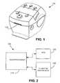
- FIG. 1is a perspective view of an illustrative thermal printer incorporating a microcontroller having flash memory in accordance with an illustrative embodiment of the present application;
- FIG. 2is a block diagram of portions of the processing system of an illustrative embodiment of the present application
- FIG. 3is a block diagram of a flash memory data block format using traditional ECC
- FIG. 4is a flowchart of a flash memory read process using a traditional ECC
- FIG. 5is a block diagram of a flash memory data block format according to an illustrative embodiment of the present application.
- FIG. 6is a flowchart of a flash memory write program according to an illustrative embodiment of the present application.
- FIG. 7is a flowchart of a flash memory read program according to an illustrative embodiment of the present application.
- ECCError Correction Constant (or Code)
- An ECCcan compensate for bit errors in flash memory.
- the software algorithmreads the flash data and ECC to RAM. If the ECC verifies, there are no bad cells. If the ECC is not correct, the software can correct the cell that is not correct if there are not too many errors.
- the data correctionincludes cells in the data or cells in the ECC itself.
- ECC algorithmsonly have a certain bit strength depending on the length of the ECC and only a certain number of bits can be corrected. A problem arises if there are more bit errors than the number that can be corrected.
- the ECCmay software may start to corrupt good cells in the flash memory.
- the typical flash memory reliability problemrelates to the physical performance parameters of the device.
- the problemis addressed by applying an ECC algorithm to the flash memory in order to maintain some (or a lot of) assurance that the output of the ECC is actually the correct value.
- the choice of the ECC bit strengthis a trade-off of at least program execution speed, memory space resource allocation and error correction and detection robustness.
- there is an additional important problem in that certain designers have decided to implement an aggressive ECC algorithmwill sometimes output a corrupted result—i.e., it outputs a valid result that meets all the “checksums” of the ECC, but it is not the correct value.
- FIG. 1a perspective view of an illustrative thermal postage printer 110 incorporating a microcontroller having flash memory in accordance with an illustrative embodiment of the present application is shown.
- Thermal media that may incorporate indicia of postage or other value paymentare printed at output port 118 .
- corrupt datacould lead to the loss of funds.
- corrupt flash memory or incorrect ECC correction manipulationmay cause good and valuable postal states to be lost.
- a microprocessor 210(or microcontroller) is used to store secure data in flash memory 230 .
- the microcontrollerincludes the 2218UF 16-bit microcontroller.
- RAM 220is used for several purposes including scratch pad memory when manipulating variables. Part or all of each of the flash memory or RAM may be internal to the microprocessor or external depending on the application.
- CMX RTOSis utilized. Additionally, as can now be appreciated, such a system may not utilize a traditional commercial embedded operating system, but may rely instead on a main executable program. Such a system may provide increased performance without the overhead of an operating system.
- a non-RTOS operating systemmay be utilized such as an embedded open source or commercial operating system.
- FIG. 3a block diagram of a 128 byte flash memory data block format 300 using traditional ECC is shown.
- User data 312is 4 8-bit Bytes wide.
- a (38, 32) Hamming codeis applied resulting in 6 bits that is stored in ECC data byte 314 .
- the other 2 bitsare not used. That 5 Byte ECC group 310 is then repeated 25 times ending in user data 332 and ECC data 334 resulting in 125 used bytes 350 in the block 300 .
- 125 used bytes100 bytes are used for User Data and 25 are used for ECC data.
- the Hamming code used in the traditional ECC implementation for the H8S/2218UF microcontrolleris the (38, 32) Hamming code in which for every 4 bytes of data, the next byte includes 6 check bits (the other two bits in every fifth byte are undefined). Accordingly, as shown in FIG. 3 , in the typical 128 Byte Block of memory, there are 25 groups of 5 bytes, each including 4 bytes of data and 1 byte of ECC check bits. The last 3 bytes of the 128 Byte Block are not used. More sophisticated ECC algorithms such as ECC200 could be utilized, but such algorithms require more processing time to execute.
- step 410the system reads a 128 Byte flash memory data block.
- the systemthen operates on each 5 byte ECC group to apply the ECC algorithm and perform error detection and correction.
- step 430the system outputs the ECC processed 100 bytes of user data.
- a microcontroller including a non-volatile flash memoryutilizes an Error Correction Code (ECC) having a certain error detection and correction bit strength.
- ECCError Correction Code
- the choice of the bit strengthis a trade-off of at least program execution speed, memory space resource allocation and error correction and detection robustness.
- the flash memoryis written in blocks of bytes such as a 128-byte block of data. Using a traditional Hamming Code (38, 32), every four bytes of data, the next byte is reserved for ECC data. Accordingly, there are then 25 ECC groups of 4 bytes data and one byte ECC data with the remaining 3 bytes typically unused. Such a system provides the ability to detect and correct 1 bit errors in the 5 byte ECC groups.
- the 100 bytes of user datais reconfigured to provide 97 bytes of user data and 3 bytes of hash data.
- the systemprocesses all of the user data (the 97 bytes of data) by performing a hash function before the ECC is applied.
- the resulting 100 bytes of user data with hash datais then processed by the ECC process to provide 125 bytes of 5 byte ECC groups. Increasing the strength of the Hamming code would be computationally and memory space prohibitive.
- the hashprovides an efficient, robust detection of incorrectly corrected user data resulting from errors beyond the correction but strength of the ECC system utilized. If the ECC incorrectly manipulated user data (or even the hash data) the hash function can be used to efficiently detect such errors. As shown herein, additional alternative illustrative embodiments are described.
- FIG. 5a block diagram of an enhanced 128 byte flash memory data block format 500 using ECC and a Hash is shown in accordance with an illustrative embodiment of FIG. 1 and the present application.
- User data 512is 4 8-bit Bytes wide.
- a (38, 32) Hamming codeis applied resulting in 6 bits that is stored in ECC data byte 514 .
- the other 2 bitsare not used. That 5 Byte ECC group 510 is then repeated 24 times ending in user data 522 and ECC data 524 .
- the 25 th ECC groupis used to provide a 4 byte portion 532 including 1 byte of user data (for a total of 97 bytes user data) and 3 bytes for Hash data along with 1 byte of ECC data 534 .
- This formatresults in 125 used bytes 550 in the block 500 .
- 97 bytesare used for User Data
- 3are used for Hash data
- 25are used for ECC data.
- Postage Sate Filesmay be defined using up to 97 bytes of data for use in a postage-printing device.
- the typically unused 3 bytes 540may be used for flag data storage. The 3 bytes 540 are not protected by the ECC system or the Hash system.
- the 3 bytes 540are used to determine if the block is empty, in use or needs to be erased. Since there are only 3 pieces of information or flags to be stored in the three bytes, there is a large amount of redundancy that can be used for error detection.
- each of the 3 bytescontain identical data, namely 0xFF, 0x55 or 0x00 to indicate the respective flag data so that the system can still determine the status of the block even if several bits of 540 are corrupt.
- step 610the system receives 97 bytes of user data such as a PSF.
- step 620the system applies the well-known SHA-1 hash algorithm to the user data. SHA-1 includes data padding algorithms and outputs a 20-byte hash result. Of that 20-byte hash result, the system in step 630 selects the 3 most significant bytes for use as hash data.
- step 640the system presents the 97 bytes of user data and appended 3 bytes of hash data to the ECC algorithm as 100 bytes of data.
- the ECC systemthen applies the A (38, 32) Hamming code resulting in 125 bytes of data used to complete the 128-byte flash data block in step 650 .
- step 660the flash memory algorithm writes that completed flash data block from RAM to the flash memory device.
- FIG. 7a flowchart of a flash memory read program 700 according to an illustrative embodiment of FIG. 1 and the present application is shown.
- a datais written to flash for the first time
- a hash of the secure datais calculated.
- an ECCis computed of the secure data and the hash.
- the hashis a unique number that can only be calculated if the secure data is completely accurate. Therefore, a more robust, but efficient ECC correction algorithm can be implemented.
- the systemreads the raw 128-byte flash memory data block including the secure data, the ECC data and the hash data.
- step 720the system applies the ECC algorithm for each 5 byte ECC group including the 97 bytes of data and the 3 bytes of hash data. In that step, if the ECC matches, the ECC portion of the algorithm terminates. If the ECC does not match, the ECC algorithm corrects the data in RAM. In step 730 , the system calculates a comparison copy of the Hash of any such corrected data in RAM. In step 740 , if the stored hash data does not match the comparison copy of the hash, the hash check fails. In step 750 , if the hash check fails, then there has been corruption in more bits than the ECC can correct. Accordingly, the system reports an error and then halts operation.
- step 760if the hash check does not fail, the system outputs 97 bytes of user data to the operating system, main program or other calling program. In an alternative, the read system exits with the 97 bytes of data if the ECC algorithm indicates correct data without defects.
- Hashprovides an efficient integrity check that allows the use of a less robust, but faster and smaller ECC system to meet the stringent performance requirements of the postage printing system.
- corrective actionmay be applied when the hash fails. If there are a small amount of bits to be tested, the application could flip each bit and then calculate a hash. Eventually it will find the corrupt bit if a single bit error has occurred.
- the ECC employedutilizes an algorithm that indicates which byte had an error. Then, each bit in the corrupt byte could be flipped and the hash can be recalculated. A matching hash would result in the error being corrected.
- the application programdetects such a hash failure, the application can also flag the error and upload the flash data to another device such as a co-located processor or a remote data center. The other device may have a backup copy of the data stored and that backup copy may then be used in order to determine where the error has occurred.
- the useful life of the flash memory deviceis increased by the illustrative embodiments described herein.
- Each flash linecan be written with a ECC and hash. Since ECC corrects bit errors, flash life can be prolonged since a defective device that causes errors can still be used while the errors can be corrected by the ECC. Using the hash extends it even longer as further corrections can be made and corruption can be avoided. This allows a flash with some bad cells or retention issues to still be used and thus, increases the life of the product that includes the flash memory device.
- ECC algorithmsare usually described generally as follows.
- a messageis written as a set of symbols or characters. These are not necessarily normal symbols; they often for example are elements of a Galois field. Additional symbols calculated using the ECC encoding algorithm are appended to the message.
- the message plus ECC symbols combinationis called a valid codeword.
- the ECC decoding algorithmfinds the “closest” valid codeword to a string of symbols. If there are too many errors, then the closest valid codeword may be incorrect. Accordingly, as described herein, there is usually a design issue regarding how robust the ECC must be and also whether false corrections can be tolerated. If the ECC is not used to correct the maximum number of errors, then the unused error correction acts as additional redundancy.
- the ECCcan handle 10 errors, but it is only used to correct up to five errors, then the extra 5 symbols provides additional redundancy that provides assurance that the message is correct.
- the ECC decodecan still give a best guess (that could very well be incorrect).
- the illustrative embodiments described hereinadd additional redundancy such as a Hash in addition to any ECC redundancy that can be checked to be sure the result of the ECC is correct.
- a hashmay be easier to calculate than a large ECC that can correct a large number of errors and therefore may be more efficient than employing a more robust ECC system.
- the ECC systemmay operate on a first size of data such as 4 bytes of user data in a 5 byte ECC group.
- the hashmay be applied across a broader data set such as the entire 97-byte user data block.
- a large hash(say 60 bits) would make it highly unlikely to ever correct something to a wrong codeword.
- the probabilityis 2 ⁇ ( ⁇ number of bits in the hash).
- a passwordcould be added into the hash that would protect against tampering with the data.
- the systemseparately generates the ECC of the data and the hash of the data.
- the ECCwill then not be used to correct the hash, which allows for more possible error correction of the data.
- the data blockis composed of a first contiguous data section followed by a 2 nd contiguous hash data section that may include all or some of the output bits of the hash algorithm, finally followed by a 3 rd contiguous ECC data section wherein the ECC algorithm processes the user data and hash data sections.
- other hash-like algorithmsmay be utilized instead of SHA-1 including cyclical redundancy check (CRC) codes and checksums.
- CRCcyclical redundancy check
- the systems and methods described hereinmay be utilized with other memory technologies including EEPROM and CMOS.
- a first error processsuch as a SHA-1 hash algorithm may be applied once to the entire user block of data and the output truncated to provide a sufficient integrity check.
- the first error processmay also be applied to subgroups of data.
- a second error processsuch as a traditional 1-bit ECC process can be applied to subgroups of data such as the 4 byte (with 1 byte ECC data) ECC groups.
- the subgroupsmay even include some user data and some hash data, all user data and/or all hash data.
- the second error processcan be applied to the entire data block or other subgroups.
- ECC algorithms or other error detection/correction algorithmsmay be utilized.
Landscapes
- Engineering & Computer Science (AREA)
- Theoretical Computer Science (AREA)
- Quality & Reliability (AREA)
- Physics & Mathematics (AREA)
- General Engineering & Computer Science (AREA)
- General Physics & Mathematics (AREA)
- Techniques For Improving Reliability Of Storages (AREA)
- Detection And Correction Of Errors (AREA)
Abstract
Description
Claims (20)
Priority Applications (1)
| Application Number | Priority Date | Filing Date | Title |
|---|---|---|---|
| US12/763,563US8010873B2 (en) | 2006-05-16 | 2010-04-20 | Systems and methods for efficient uncorrectable error detection in flash memory |
Applications Claiming Priority (2)
| Application Number | Priority Date | Filing Date | Title |
|---|---|---|---|
| US11/436,171US7707481B2 (en) | 2006-05-16 | 2006-05-16 | System and method for efficient uncorrectable error detection in flash memory |
| US12/763,563US8010873B2 (en) | 2006-05-16 | 2010-04-20 | Systems and methods for efficient uncorrectable error detection in flash memory |
Related Parent Applications (1)
| Application Number | Title | Priority Date | Filing Date |
|---|---|---|---|
| US11/436,171ContinuationUS7707481B2 (en) | 2006-05-16 | 2006-05-16 | System and method for efficient uncorrectable error detection in flash memory |
Publications (2)
| Publication Number | Publication Date |
|---|---|
| US20100205509A1 US20100205509A1 (en) | 2010-08-12 |
| US8010873B2true US8010873B2 (en) | 2011-08-30 |
Family
ID=38515708
Family Applications (2)
| Application Number | Title | Priority Date | Filing Date |
|---|---|---|---|
| US11/436,171Expired - Fee RelatedUS7707481B2 (en) | 2006-05-16 | 2006-05-16 | System and method for efficient uncorrectable error detection in flash memory |
| US12/763,563Expired - Fee RelatedUS8010873B2 (en) | 2006-05-16 | 2010-04-20 | Systems and methods for efficient uncorrectable error detection in flash memory |
Family Applications Before (1)
| Application Number | Title | Priority Date | Filing Date |
|---|---|---|---|
| US11/436,171Expired - Fee RelatedUS7707481B2 (en) | 2006-05-16 | 2006-05-16 | System and method for efficient uncorrectable error detection in flash memory |
Country Status (3)
| Country | Link |
|---|---|
| US (2) | US7707481B2 (en) |
| EP (1) | EP1857939B1 (en) |
| CA (1) | CA2588858A1 (en) |
Cited By (5)
| Publication number | Priority date | Publication date | Assignee | Title |
|---|---|---|---|---|
| US20110047421A1 (en)* | 2009-08-24 | 2011-02-24 | Ocz Technology Group, Inc. | Nand flash-based storage device with built-in test-ahead for failure anticipation |
| US8812935B2 (en) | 2012-08-02 | 2014-08-19 | Oracle International Corporation | Using a data ECC to detect address corruption |
| US9213598B2 (en) | 2013-02-19 | 2015-12-15 | Samsung Electronics Co., Ltd. | Nonvolatile memory device and method of operating the same |
| US11756643B2 (en) | 2020-10-05 | 2023-09-12 | SK Hynix Inc. | Apparatus and method for correcting an error in data transmission of a data processing system |
| US11854612B1 (en) | 2011-07-19 | 2023-12-26 | Vervain, Llc | Lifetime mixed level non-volatile memory system |
Families Citing this family (112)
| Publication number | Priority date | Publication date | Assignee | Title |
|---|---|---|---|---|
| US6735253B1 (en) | 1997-05-16 | 2004-05-11 | The Trustees Of Columbia University In The City Of New York | Methods and architecture for indexing and editing compressed video over the world wide web |
| WO2006096612A2 (en) | 2005-03-04 | 2006-09-14 | The Trustees Of Columbia University In The City Of New York | System and method for motion estimation and mode decision for low-complexity h.264 decoder |
| US8316258B2 (en)* | 2007-05-03 | 2012-11-20 | Oracle America, Inc. | System and method for error detection in a data storage system |
| US7770079B2 (en)* | 2007-08-22 | 2010-08-03 | Micron Technology Inc. | Error scanning in flash memory |
| JP4564520B2 (en)* | 2007-08-31 | 2010-10-20 | 株式会社東芝 | Semiconductor memory device and control method thereof |
| US20090113166A1 (en)* | 2007-10-31 | 2009-04-30 | Agere Systems Inc. | Hashing method for nand flash memory |
| US8762620B2 (en)* | 2007-12-27 | 2014-06-24 | Sandisk Enterprise Ip Llc | Multiprocessor storage controller |
| WO2009126785A2 (en) | 2008-04-10 | 2009-10-15 | The Trustees Of Columbia University In The City Of New York | Systems and methods for image archaeology |
| US8347111B2 (en)* | 2009-01-06 | 2013-01-01 | Hewlett-Packard Development Company, L.P. | Data processing apparatus |
| US20100174920A1 (en)* | 2009-01-06 | 2010-07-08 | Jonathan Peter Buckingham | Data processing apparatus |
| US8365041B2 (en) | 2010-03-17 | 2013-01-29 | Sandisk Enterprise Ip Llc | MLC self-raid flash data protection scheme |
| US8418026B2 (en)* | 2010-10-27 | 2013-04-09 | Sandisk Technologies Inc. | Hybrid error correction coding to address uncorrectable errors |
| JP2012252557A (en)* | 2011-06-03 | 2012-12-20 | Mega Chips Corp | Memory controller |
| US8909982B2 (en) | 2011-06-19 | 2014-12-09 | Sandisk Enterprise Ip Llc | System and method for detecting copyback programming problems |
| US8910020B2 (en) | 2011-06-19 | 2014-12-09 | Sandisk Enterprise Ip Llc | Intelligent bit recovery for flash memory |
| JP2013003983A (en)* | 2011-06-20 | 2013-01-07 | Toshiba Corp | Memory control device and memory control method |
| US8938658B2 (en) | 2011-11-07 | 2015-01-20 | Sandisk Enterprise Ip Llc | Statistical read comparison signal generation for memory systems |
| US9048876B2 (en) | 2011-11-18 | 2015-06-02 | Sandisk Enterprise Ip Llc | Systems, methods and devices for multi-tiered error correction |
| US8924815B2 (en) | 2011-11-18 | 2014-12-30 | Sandisk Enterprise Ip Llc | Systems, methods and devices for decoding codewords having multiple parity segments |
| US8954822B2 (en) | 2011-11-18 | 2015-02-10 | Sandisk Enterprise Ip Llc | Data encoder and decoder using memory-specific parity-check matrix |
| US9009149B2 (en)* | 2011-12-06 | 2015-04-14 | The Trustees Of Columbia University In The City Of New York | Systems and methods for mobile search using Bag of Hash Bits and boundary reranking |
| US9699263B1 (en) | 2012-08-17 | 2017-07-04 | Sandisk Technologies Llc. | Automatic read and write acceleration of data accessed by virtual machines |
| US9501398B2 (en) | 2012-12-26 | 2016-11-22 | Sandisk Technologies Llc | Persistent storage device with NVRAM for staging writes |
| US9612948B2 (en) | 2012-12-27 | 2017-04-04 | Sandisk Technologies Llc | Reads and writes between a contiguous data block and noncontiguous sets of logical address blocks in a persistent storage device |
| US9239751B1 (en) | 2012-12-27 | 2016-01-19 | Sandisk Enterprise Ip Llc | Compressing data from multiple reads for error control management in memory systems |
| US9454420B1 (en) | 2012-12-31 | 2016-09-27 | Sandisk Technologies Llc | Method and system of reading threshold voltage equalization |
| US9003264B1 (en) | 2012-12-31 | 2015-04-07 | Sandisk Enterprise Ip Llc | Systems, methods, and devices for multi-dimensional flash RAID data protection |
| US9141554B1 (en) | 2013-01-18 | 2015-09-22 | Cisco Technology, Inc. | Methods and apparatus for data processing using data compression, linked lists and de-duplication techniques |
| US9329928B2 (en) | 2013-02-20 | 2016-05-03 | Sandisk Enterprise IP LLC. | Bandwidth optimization in a non-volatile memory system |
| US9214965B2 (en) | 2013-02-20 | 2015-12-15 | Sandisk Enterprise Ip Llc | Method and system for improving data integrity in non-volatile storage |
| US9870830B1 (en) | 2013-03-14 | 2018-01-16 | Sandisk Technologies Llc | Optimal multilevel sensing for reading data from a storage medium |
| US9448877B2 (en)* | 2013-03-15 | 2016-09-20 | Cisco Technology, Inc. | Methods and apparatus for error detection and correction in data storage systems using hash value comparisons |
| US9367246B2 (en) | 2013-03-15 | 2016-06-14 | Sandisk Technologies Inc. | Performance optimization of data transfer for soft information generation |
| US9009576B1 (en) | 2013-03-15 | 2015-04-14 | Sandisk Enterprise Ip Llc | Adaptive LLR based on syndrome weight |
| US9244763B1 (en) | 2013-03-15 | 2016-01-26 | Sandisk Enterprise Ip Llc | System and method for updating a reading threshold voltage based on symbol transition information |
| US9236886B1 (en) | 2013-03-15 | 2016-01-12 | Sandisk Enterprise Ip Llc | Universal and reconfigurable QC-LDPC encoder |
| US9092350B1 (en) | 2013-03-15 | 2015-07-28 | Sandisk Enterprise Ip Llc | Detection and handling of unbalanced errors in interleaved codewords |
| US9136877B1 (en) | 2013-03-15 | 2015-09-15 | Sandisk Enterprise Ip Llc | Syndrome layered decoding for LDPC codes |
| US9170941B2 (en) | 2013-04-05 | 2015-10-27 | Sandisk Enterprises IP LLC | Data hardening in a storage system |
| US10049037B2 (en) | 2013-04-05 | 2018-08-14 | Sandisk Enterprise Ip Llc | Data management in a storage system |
| US9159437B2 (en) | 2013-06-11 | 2015-10-13 | Sandisk Enterprise IP LLC. | Device and method for resolving an LM flag issue |
| US9384126B1 (en) | 2013-07-25 | 2016-07-05 | Sandisk Technologies Inc. | Methods and systems to avoid false negative results in bloom filters implemented in non-volatile data storage systems |
| US9524235B1 (en) | 2013-07-25 | 2016-12-20 | Sandisk Technologies Llc | Local hash value generation in non-volatile data storage systems |
| US9043517B1 (en) | 2013-07-25 | 2015-05-26 | Sandisk Enterprise Ip Llc | Multipass programming in buffers implemented in non-volatile data storage systems |
| US9361221B1 (en) | 2013-08-26 | 2016-06-07 | Sandisk Technologies Inc. | Write amplification reduction through reliable writes during garbage collection |
| US9639463B1 (en) | 2013-08-26 | 2017-05-02 | Sandisk Technologies Llc | Heuristic aware garbage collection scheme in storage systems |
| US9442670B2 (en) | 2013-09-03 | 2016-09-13 | Sandisk Technologies Llc | Method and system for rebalancing data stored in flash memory devices |
| US9519577B2 (en) | 2013-09-03 | 2016-12-13 | Sandisk Technologies Llc | Method and system for migrating data between flash memory devices |
| US9158349B2 (en) | 2013-10-04 | 2015-10-13 | Sandisk Enterprise Ip Llc | System and method for heat dissipation |
| US9323637B2 (en) | 2013-10-07 | 2016-04-26 | Sandisk Enterprise Ip Llc | Power sequencing and data hardening architecture |
| US9298608B2 (en) | 2013-10-18 | 2016-03-29 | Sandisk Enterprise Ip Llc | Biasing for wear leveling in storage systems |
| US9442662B2 (en) | 2013-10-18 | 2016-09-13 | Sandisk Technologies Llc | Device and method for managing die groups |
| US9436831B2 (en) | 2013-10-30 | 2016-09-06 | Sandisk Technologies Llc | Secure erase in a memory device |
| US9263156B2 (en) | 2013-11-07 | 2016-02-16 | Sandisk Enterprise Ip Llc | System and method for adjusting trip points within a storage device |
| US9244785B2 (en) | 2013-11-13 | 2016-01-26 | Sandisk Enterprise Ip Llc | Simulated power failure and data hardening |
| US9152555B2 (en) | 2013-11-15 | 2015-10-06 | Sandisk Enterprise IP LLC. | Data management with modular erase in a data storage system |
| US9703816B2 (en) | 2013-11-19 | 2017-07-11 | Sandisk Technologies Llc | Method and system for forward reference logging in a persistent datastore |
| US9520197B2 (en) | 2013-11-22 | 2016-12-13 | Sandisk Technologies Llc | Adaptive erase of a storage device |
| US9122636B2 (en) | 2013-11-27 | 2015-09-01 | Sandisk Enterprise Ip Llc | Hard power fail architecture |
| US9280429B2 (en) | 2013-11-27 | 2016-03-08 | Sandisk Enterprise Ip Llc | Power fail latching based on monitoring multiple power supply voltages in a storage device |
| US9520162B2 (en) | 2013-11-27 | 2016-12-13 | Sandisk Technologies Llc | DIMM device controller supervisor |
| US9250676B2 (en) | 2013-11-29 | 2016-02-02 | Sandisk Enterprise Ip Llc | Power failure architecture and verification |
| US9582058B2 (en) | 2013-11-29 | 2017-02-28 | Sandisk Technologies Llc | Power inrush management of storage devices |
| US9092370B2 (en) | 2013-12-03 | 2015-07-28 | Sandisk Enterprise Ip Llc | Power failure tolerant cryptographic erase |
| US9235245B2 (en) | 2013-12-04 | 2016-01-12 | Sandisk Enterprise Ip Llc | Startup performance and power isolation |
| US9129665B2 (en) | 2013-12-17 | 2015-09-08 | Sandisk Enterprise Ip Llc | Dynamic brownout adjustment in a storage device |
| US9549457B2 (en) | 2014-02-12 | 2017-01-17 | Sandisk Technologies Llc | System and method for redirecting airflow across an electronic assembly |
| US9497889B2 (en) | 2014-02-27 | 2016-11-15 | Sandisk Technologies Llc | Heat dissipation for substrate assemblies |
| US9703636B2 (en) | 2014-03-01 | 2017-07-11 | Sandisk Technologies Llc | Firmware reversion trigger and control |
| US9485851B2 (en) | 2014-03-14 | 2016-11-01 | Sandisk Technologies Llc | Thermal tube assembly structures |
| US9519319B2 (en) | 2014-03-14 | 2016-12-13 | Sandisk Technologies Llc | Self-supporting thermal tube structure for electronic assemblies |
| US9348377B2 (en) | 2014-03-14 | 2016-05-24 | Sandisk Enterprise Ip Llc | Thermal isolation techniques |
| US9448876B2 (en) | 2014-03-19 | 2016-09-20 | Sandisk Technologies Llc | Fault detection and prediction in storage devices |
| US9454448B2 (en) | 2014-03-19 | 2016-09-27 | Sandisk Technologies Llc | Fault testing in storage devices |
| US9390814B2 (en) | 2014-03-19 | 2016-07-12 | Sandisk Technologies Llc | Fault detection and prediction for data storage elements |
| US9626400B2 (en) | 2014-03-31 | 2017-04-18 | Sandisk Technologies Llc | Compaction of information in tiered data structure |
| US9390021B2 (en) | 2014-03-31 | 2016-07-12 | Sandisk Technologies Llc | Efficient cache utilization in a tiered data structure |
| US9626399B2 (en) | 2014-03-31 | 2017-04-18 | Sandisk Technologies Llc | Conditional updates for reducing frequency of data modification operations |
| US9697267B2 (en) | 2014-04-03 | 2017-07-04 | Sandisk Technologies Llc | Methods and systems for performing efficient snapshots in tiered data structures |
| US9703491B2 (en) | 2014-05-30 | 2017-07-11 | Sandisk Technologies Llc | Using history of unaligned writes to cache data and avoid read-modify-writes in a non-volatile storage device |
| US9093160B1 (en) | 2014-05-30 | 2015-07-28 | Sandisk Technologies Inc. | Methods and systems for staggered memory operations |
| US10372613B2 (en) | 2014-05-30 | 2019-08-06 | Sandisk Technologies Llc | Using sub-region I/O history to cache repeatedly accessed sub-regions in a non-volatile storage device |
| US10146448B2 (en) | 2014-05-30 | 2018-12-04 | Sandisk Technologies Llc | Using history of I/O sequences to trigger cached read ahead in a non-volatile storage device |
| US10656840B2 (en) | 2014-05-30 | 2020-05-19 | Sandisk Technologies Llc | Real-time I/O pattern recognition to enhance performance and endurance of a storage device |
| US10114557B2 (en) | 2014-05-30 | 2018-10-30 | Sandisk Technologies Llc | Identification of hot regions to enhance performance and endurance of a non-volatile storage device |
| US9645749B2 (en) | 2014-05-30 | 2017-05-09 | Sandisk Technologies Llc | Method and system for recharacterizing the storage density of a memory device or a portion thereof |
| US10656842B2 (en) | 2014-05-30 | 2020-05-19 | Sandisk Technologies Llc | Using history of I/O sizes and I/O sequences to trigger coalesced writes in a non-volatile storage device |
| US9070481B1 (en) | 2014-05-30 | 2015-06-30 | Sandisk Technologies Inc. | Internal current measurement for age measurements |
| US8891303B1 (en) | 2014-05-30 | 2014-11-18 | Sandisk Technologies Inc. | Method and system for dynamic word line based configuration of a three-dimensional memory device |
| US10162748B2 (en) | 2014-05-30 | 2018-12-25 | Sandisk Technologies Llc | Prioritizing garbage collection and block allocation based on I/O history for logical address regions |
| US9652381B2 (en) | 2014-06-19 | 2017-05-16 | Sandisk Technologies Llc | Sub-block garbage collection |
| US9443601B2 (en) | 2014-09-08 | 2016-09-13 | Sandisk Technologies Llc | Holdup capacitor energy harvesting |
| US9853873B2 (en) | 2015-01-10 | 2017-12-26 | Cisco Technology, Inc. | Diagnosis and throughput measurement of fibre channel ports in a storage area network environment |
| US9900250B2 (en) | 2015-03-26 | 2018-02-20 | Cisco Technology, Inc. | Scalable handling of BGP route information in VXLAN with EVPN control plane |
| US10222986B2 (en) | 2015-05-15 | 2019-03-05 | Cisco Technology, Inc. | Tenant-level sharding of disks with tenant-specific storage modules to enable policies per tenant in a distributed storage system |
| US11588783B2 (en) | 2015-06-10 | 2023-02-21 | Cisco Technology, Inc. | Techniques for implementing IPV6-based distributed storage space |
| US10778765B2 (en) | 2015-07-15 | 2020-09-15 | Cisco Technology, Inc. | Bid/ask protocol in scale-out NVMe storage |
| FR3040523B1 (en) | 2015-08-28 | 2018-07-13 | Continental Automotive France | METHOD OF DETECTING AN UNCOMPRIGIBLE ERROR IN A NON-VOLATILE MEMORY OF A MICROCONTROLLER |
| US9892075B2 (en) | 2015-12-10 | 2018-02-13 | Cisco Technology, Inc. | Policy driven storage in a microserver computing environment |
| US10140172B2 (en) | 2016-05-18 | 2018-11-27 | Cisco Technology, Inc. | Network-aware storage repairs |
| US20170351639A1 (en) | 2016-06-06 | 2017-12-07 | Cisco Technology, Inc. | Remote memory access using memory mapped addressing among multiple compute nodes |
| US10664169B2 (en) | 2016-06-24 | 2020-05-26 | Cisco Technology, Inc. | Performance of object storage system by reconfiguring storage devices based on latency that includes identifying a number of fragments that has a particular storage device as its primary storage device and another number of fragments that has said particular storage device as its replica storage device |
| US11563695B2 (en) | 2016-08-29 | 2023-01-24 | Cisco Technology, Inc. | Queue protection using a shared global memory reserve |
| US10365961B2 (en)* | 2016-09-09 | 2019-07-30 | Dell Products L.P. | Information handling system pre-boot fault management |
| US10545914B2 (en) | 2017-01-17 | 2020-01-28 | Cisco Technology, Inc. | Distributed object storage |
| US10243823B1 (en) | 2017-02-24 | 2019-03-26 | Cisco Technology, Inc. | Techniques for using frame deep loopback capabilities for extended link diagnostics in fibre channel storage area networks |
| US10713203B2 (en) | 2017-02-28 | 2020-07-14 | Cisco Technology, Inc. | Dynamic partition of PCIe disk arrays based on software configuration / policy distribution |
| US10254991B2 (en) | 2017-03-06 | 2019-04-09 | Cisco Technology, Inc. | Storage area network based extended I/O metrics computation for deep insight into application performance |
| US10303534B2 (en) | 2017-07-20 | 2019-05-28 | Cisco Technology, Inc. | System and method for self-healing of application centric infrastructure fabric memory |
| US10404596B2 (en) | 2017-10-03 | 2019-09-03 | Cisco Technology, Inc. | Dynamic route profile storage in a hardware trie routing table |
| US10942666B2 (en) | 2017-10-13 | 2021-03-09 | Cisco Technology, Inc. | Using network device replication in distributed storage clusters |
| CN115459882A (en)* | 2022-09-05 | 2022-12-09 | 福建天晴在线互动科技有限公司 | Remote file repair method and system |
Citations (13)
| Publication number | Priority date | Publication date | Assignee | Title |
|---|---|---|---|---|
| US5357527A (en) | 1992-12-31 | 1994-10-18 | Trimble Navigation Limited | Validation of RAM-resident software programs |
| US5734663A (en) | 1991-12-18 | 1998-03-31 | International Business Machines Corporation | Abbreviated trial-and-error technique for correcting long bursts of consecutive errors using CRC bytes |
| US6041001A (en) | 1999-02-25 | 2000-03-21 | Lexar Media, Inc. | Method of increasing data reliability of a flash memory device without compromising compatibility |
| US6334201B1 (en)* | 1997-06-12 | 2001-12-25 | Hitachi, Ltd. | Decoding circuit and information processing apparatus |
| US6438706B1 (en) | 1995-10-31 | 2002-08-20 | Intel Corporation | On chip error correction for devices in a solid state drive |
| US6625061B2 (en) | 2000-10-25 | 2003-09-23 | Fujitsu Limited | Method of managing a defect in a flash memory |
| US20040128511A1 (en) | 2000-12-20 | 2004-07-01 | Qibin Sun | Methods and systems for generating multimedia signature |
| WO2004066296A1 (en) | 2003-01-24 | 2004-08-05 | Koninklijke Philips Electronics N.V. | Reliable storage medium access control method and device |
| US20050086504A1 (en) | 2003-10-17 | 2005-04-21 | Samsung Electronics Co., Ltd. | Method of authenticating device using certificate, and digital content processing device for performing device authentication using the same |
| US6959384B1 (en) | 1999-12-14 | 2005-10-25 | Intertrust Technologies Corporation | Systems and methods for authenticating and protecting the integrity of data streams and other data |
| US20060156187A1 (en)* | 2004-12-29 | 2006-07-13 | National Tsing Hua University | Method and apparatus for multiple polynomial-based random number generation |
| US20060161567A1 (en) | 2005-01-14 | 2006-07-20 | Microsoft Corporation | Low communication complexity memory-bound function |
| US20070150790A1 (en)* | 2005-12-27 | 2007-06-28 | Gross Stephen J | Method of storing downloadable firmware on bulk media |
Family Cites Families (2)
| Publication number | Priority date | Publication date | Assignee | Title |
|---|---|---|---|---|
| US6959984B2 (en)* | 2001-08-14 | 2005-11-01 | Canon Kabushiki Kaisha | Liquid container and inkjet cartridge |
| JP2003346432A (en)* | 2002-05-22 | 2003-12-05 | Internatl Business Mach Corp <Ibm> | Data storage device and data processing method |
- 2006
- 2006-05-16USUS11/436,171patent/US7707481B2/ennot_activeExpired - Fee Related
- 2007
- 2007-05-15CACA002588858Apatent/CA2588858A1/ennot_activeAbandoned
- 2007-05-15EPEP07009691.2Apatent/EP1857939B1/ennot_activeNot-in-force
- 2010
- 2010-04-20USUS12/763,563patent/US8010873B2/ennot_activeExpired - Fee Related
Patent Citations (13)
| Publication number | Priority date | Publication date | Assignee | Title |
|---|---|---|---|---|
| US5734663A (en) | 1991-12-18 | 1998-03-31 | International Business Machines Corporation | Abbreviated trial-and-error technique for correcting long bursts of consecutive errors using CRC bytes |
| US5357527A (en) | 1992-12-31 | 1994-10-18 | Trimble Navigation Limited | Validation of RAM-resident software programs |
| US6438706B1 (en) | 1995-10-31 | 2002-08-20 | Intel Corporation | On chip error correction for devices in a solid state drive |
| US6334201B1 (en)* | 1997-06-12 | 2001-12-25 | Hitachi, Ltd. | Decoding circuit and information processing apparatus |
| US6041001A (en) | 1999-02-25 | 2000-03-21 | Lexar Media, Inc. | Method of increasing data reliability of a flash memory device without compromising compatibility |
| US6959384B1 (en) | 1999-12-14 | 2005-10-25 | Intertrust Technologies Corporation | Systems and methods for authenticating and protecting the integrity of data streams and other data |
| US6625061B2 (en) | 2000-10-25 | 2003-09-23 | Fujitsu Limited | Method of managing a defect in a flash memory |
| US20040128511A1 (en) | 2000-12-20 | 2004-07-01 | Qibin Sun | Methods and systems for generating multimedia signature |
| WO2004066296A1 (en) | 2003-01-24 | 2004-08-05 | Koninklijke Philips Electronics N.V. | Reliable storage medium access control method and device |
| US20050086504A1 (en) | 2003-10-17 | 2005-04-21 | Samsung Electronics Co., Ltd. | Method of authenticating device using certificate, and digital content processing device for performing device authentication using the same |
| US20060156187A1 (en)* | 2004-12-29 | 2006-07-13 | National Tsing Hua University | Method and apparatus for multiple polynomial-based random number generation |
| US20060161567A1 (en) | 2005-01-14 | 2006-07-20 | Microsoft Corporation | Low communication complexity memory-bound function |
| US20070150790A1 (en)* | 2005-12-27 | 2007-06-28 | Gross Stephen J | Method of storing downloadable firmware on bulk media |
Non-Patent Citations (1)
| Title |
|---|
| Renesas, Application Note, H8S/2215 Group, 0.35-um F-ZTAT Software ECC Programming., REJ06B0139-O200O/ Rev. 2.00 Mar. 2004, pp. 1-28. |
Cited By (11)
| Publication number | Priority date | Publication date | Assignee | Title |
|---|---|---|---|---|
| US20110047421A1 (en)* | 2009-08-24 | 2011-02-24 | Ocz Technology Group, Inc. | Nand flash-based storage device with built-in test-ahead for failure anticipation |
| US8910002B2 (en)* | 2009-08-24 | 2014-12-09 | OCZ Storage Solutions Inc. | NAND flash-based storage device with built-in test-ahead for failure anticipation |
| US11854612B1 (en) | 2011-07-19 | 2023-12-26 | Vervain, Llc | Lifetime mixed level non-volatile memory system |
| US11967370B1 (en) | 2011-07-19 | 2024-04-23 | Vervain, Llc | Lifetime mixed level non-volatile memory system |
| US11967369B2 (en) | 2011-07-19 | 2024-04-23 | Vervain, Llc | Lifetime mixed level non-volatile memory system |
| US12119054B2 (en) | 2011-07-19 | 2024-10-15 | Vervain, Llc | Lifetime mixed level non-volatile memory system |
| US12136455B2 (en) | 2011-07-19 | 2024-11-05 | Vervain, Llc | Lifetime mixed level non-volatile memory system |
| US12224005B1 (en) | 2011-07-19 | 2025-02-11 | Vervain, Llc | Lifetime mixed level non-volatile memory system |
| US8812935B2 (en) | 2012-08-02 | 2014-08-19 | Oracle International Corporation | Using a data ECC to detect address corruption |
| US9213598B2 (en) | 2013-02-19 | 2015-12-15 | Samsung Electronics Co., Ltd. | Nonvolatile memory device and method of operating the same |
| US11756643B2 (en) | 2020-10-05 | 2023-09-12 | SK Hynix Inc. | Apparatus and method for correcting an error in data transmission of a data processing system |
Also Published As
| Publication number | Publication date |
|---|---|
| CA2588858A1 (en) | 2007-11-16 |
| EP1857939A3 (en) | 2008-07-30 |
| US20070283224A1 (en) | 2007-12-06 |
| EP1857939B1 (en) | 2019-12-18 |
| EP1857939A2 (en) | 2007-11-21 |
| US20100205509A1 (en) | 2010-08-12 |
| US7707481B2 (en) | 2010-04-27 |
Similar Documents
| Publication | Publication Date | Title |
|---|---|---|
| US8010873B2 (en) | Systems and methods for efficient uncorrectable error detection in flash memory | |
| US8635510B2 (en) | Non-systematic coded error correction | |
| KR100645058B1 (en) | Memory Management Techniques to Improve Data Reliability | |
| US8065583B2 (en) | Data storage with an outer block code and a stream-based inner code | |
| EP2673709B1 (en) | Data recovery using additional error correction coding data | |
| US9043678B2 (en) | Detecting effect of corrupting event on preloaded data in non-volatile memory | |
| US7930612B2 (en) | Error detection and correction scheme for a memory device | |
| US8719677B2 (en) | Using ECC encoding to verify an ECC decode operation | |
| US20100251066A1 (en) | Data handling | |
| US20070283214A1 (en) | Corruption-resistant data porting with multiple error correction schemes | |
| KR20100033507A (en) | Emerging bad block detection | |
| CN101373640A (en) | Flash memory device and error correction method | |
| US10191801B2 (en) | Error correction code management of write-once memory codes | |
| US20030081468A1 (en) | Method and device for backing up data in a memory module and memory module | |
| JPH02146200A (en) | Eeprom device | |
| CN112151104B (en) | Memory storage device and dynamic data restoration method thereof | |
| US20230297244A1 (en) | Error correction code offload for a serially-attached memory device | |
| CN119339774A (en) | A method and device for online error correction of FLASH system for laser communication | |
| CN114237493A (en) | Modular storage method and system in embedded system | |
| JP2007179480A (en) | Memory controller and flash memory system | |
| HU180131B (en) | Device for increasing reliability of the operative store of computers |
Legal Events
| Date | Code | Title | Description |
|---|---|---|---|
| AS | Assignment | Owner name:PITNEY BOWES INC., CONNECTICUT Free format text:ASSIGNMENT OF ASSIGNORS INTEREST;ASSIGNORS:KIRSCHNER, WESLEY A.;SISSON, ROBERT W.;HURD, JOHN A.;AND OTHERS;REEL/FRAME:024259/0727 Effective date:20060516 | |
| ZAAA | Notice of allowance and fees due | Free format text:ORIGINAL CODE: NOA | |
| ZAAB | Notice of allowance mailed | Free format text:ORIGINAL CODE: MN/=. | |
| STCF | Information on status: patent grant | Free format text:PATENTED CASE | |
| FPAY | Fee payment | Year of fee payment:4 | |
| MAFP | Maintenance fee payment | Free format text:PAYMENT OF MAINTENANCE FEE, 8TH YEAR, LARGE ENTITY (ORIGINAL EVENT CODE: M1552); ENTITY STATUS OF PATENT OWNER: LARGE ENTITY Year of fee payment:8 | |
| AS | Assignment | Owner name:JPMORGAN CHASE BANK, N.A., AS ADMINISTRATIVE AGENT Free format text:SECURITY INTEREST;ASSIGNORS:PITNEY BOWES INC.;NEWGISTICS, INC.;BORDERFREE, INC.;AND OTHERS;REEL/FRAME:050905/0640 Effective date:20191101 Owner name:JPMORGAN CHASE BANK, N.A., AS ADMINISTRATIVE AGENT, NEW YORK Free format text:SECURITY INTEREST;ASSIGNORS:PITNEY BOWES INC.;NEWGISTICS, INC.;BORDERFREE, INC.;AND OTHERS;REEL/FRAME:050905/0640 Effective date:20191101 | |
| FEPP | Fee payment procedure | Free format text:MAINTENANCE FEE REMINDER MAILED (ORIGINAL EVENT CODE: REM.); ENTITY STATUS OF PATENT OWNER: LARGE ENTITY | |
| LAPS | Lapse for failure to pay maintenance fees | Free format text:PATENT EXPIRED FOR FAILURE TO PAY MAINTENANCE FEES (ORIGINAL EVENT CODE: EXP.); ENTITY STATUS OF PATENT OWNER: LARGE ENTITY | |
| STCH | Information on status: patent discontinuation | Free format text:PATENT EXPIRED DUE TO NONPAYMENT OF MAINTENANCE FEES UNDER 37 CFR 1.362 | |
| FP | Lapsed due to failure to pay maintenance fee | Effective date:20230830 | |
| AS | Assignment | Owner name:PITNEY BOWES, INC., CONNECTICUT Free format text:RELEASE OF PATENT SECURITY AGREEMENT;ASSIGNOR:JPMORGAN CHASE BANK, N.A., AS ADMINISTRATIVE AGENT;REEL/FRAME:070256/0396 Effective date:20250207 |