US8008759B2 - Pre-molded clip structure - Google Patents
Pre-molded clip structureDownload PDFInfo
- Publication number
- US8008759B2 US8008759B2US12/822,932US82293210AUS8008759B2US 8008759 B2US8008759 B2US 8008759B2US 82293210 AUS82293210 AUS 82293210AUS 8008759 B2US8008759 B2US 8008759B2
- Authority
- US
- United States
- Prior art keywords
- clip
- molding material
- semiconductor die
- package
- die
- Prior art date
- Legal status (The legal status is an assumption and is not a legal conclusion. Google has not performed a legal analysis and makes no representation as to the accuracy of the status listed.)
- Active
Links
- 239000012778molding materialSubstances0.000claimsabstractdescription59
- 239000004065semiconductorSubstances0.000claimsdescription61
- RYGMFSIKBFXOCR-UHFFFAOYSA-NCopperChemical compound[Cu]RYGMFSIKBFXOCR-UHFFFAOYSA-N0.000claimsdescription10
- 229910052802copperInorganic materials0.000claimsdescription10
- 239000010949copperSubstances0.000claimsdescription10
- 238000000034methodMethods0.000abstractdescription32
- 230000008569processEffects0.000description22
- 238000000465mouldingMethods0.000description9
- 229910000679solderInorganic materials0.000description8
- 238000005530etchingMethods0.000description7
- 239000000853adhesiveSubstances0.000description6
- 230000001070adhesive effectEffects0.000description6
- 238000013461designMethods0.000description6
- 239000004593EpoxySubstances0.000description4
- 239000000463materialSubstances0.000description3
- 238000012545processingMethods0.000description3
- 238000005476solderingMethods0.000description3
- 239000004020conductorSubstances0.000description2
- 229910052751metalInorganic materials0.000description2
- 239000002184metalSubstances0.000description2
- 229910000510noble metalInorganic materials0.000description2
- 238000004806packaging method and processMethods0.000description2
- 238000013459approachMethods0.000description1
- 230000008901benefitEffects0.000description1
- 230000001413cellular effectEffects0.000description1
- 238000004140cleaningMethods0.000description1
- 239000002131composite materialSubstances0.000description1
- 150000001875compoundsChemical class0.000description1
- 238000009792diffusion processMethods0.000description1
- 230000004907fluxEffects0.000description1
- 230000017525heat dissipationEffects0.000description1
- 239000011159matrix materialSubstances0.000description1
- 239000007769metal materialSubstances0.000description1
- 150000002739metalsChemical class0.000description1
- 230000037361pathwayEffects0.000description1
- 238000012552reviewMethods0.000description1
- 239000000758substrateSubstances0.000description1
- 238000012360testing methodMethods0.000description1
- 239000003039volatile agentSubstances0.000description1
Images


Classifications
- H—ELECTRICITY
- H01—ELECTRIC ELEMENTS
- H01L—SEMICONDUCTOR DEVICES NOT COVERED BY CLASS H10
- H01L23/00—Details of semiconductor or other solid state devices
- H01L23/48—Arrangements for conducting electric current to or from the solid state body in operation, e.g. leads, terminal arrangements ; Selection of materials therefor
- H01L23/488—Arrangements for conducting electric current to or from the solid state body in operation, e.g. leads, terminal arrangements ; Selection of materials therefor consisting of soldered or bonded constructions
- H01L23/495—Lead-frames or other flat leads
- H01L23/49541—Geometry of the lead-frame
- H01L23/49562—Geometry of the lead-frame for individual devices of subclass H10D
- H—ELECTRICITY
- H01—ELECTRIC ELEMENTS
- H01L—SEMICONDUCTOR DEVICES NOT COVERED BY CLASS H10
- H01L23/00—Details of semiconductor or other solid state devices
- H01L23/48—Arrangements for conducting electric current to or from the solid state body in operation, e.g. leads, terminal arrangements ; Selection of materials therefor
- H01L23/488—Arrangements for conducting electric current to or from the solid state body in operation, e.g. leads, terminal arrangements ; Selection of materials therefor consisting of soldered or bonded constructions
- H01L23/495—Lead-frames or other flat leads
- H01L23/49517—Additional leads
- H01L23/49524—Additional leads the additional leads being a tape carrier or flat leads
- H—ELECTRICITY
- H01—ELECTRIC ELEMENTS
- H01L—SEMICONDUCTOR DEVICES NOT COVERED BY CLASS H10
- H01L23/00—Details of semiconductor or other solid state devices
- H01L23/48—Arrangements for conducting electric current to or from the solid state body in operation, e.g. leads, terminal arrangements ; Selection of materials therefor
- H01L23/488—Arrangements for conducting electric current to or from the solid state body in operation, e.g. leads, terminal arrangements ; Selection of materials therefor consisting of soldered or bonded constructions
- H01L23/495—Lead-frames or other flat leads
- H01L23/49575—Assemblies of semiconductor devices on lead frames
- H—ELECTRICITY
- H01—ELECTRIC ELEMENTS
- H01L—SEMICONDUCTOR DEVICES NOT COVERED BY CLASS H10
- H01L24/00—Arrangements for connecting or disconnecting semiconductor or solid-state bodies; Methods or apparatus related thereto
- H01L24/01—Means for bonding being attached to, or being formed on, the surface to be connected, e.g. chip-to-package, die-attach, "first-level" interconnects; Manufacturing methods related thereto
- H01L24/34—Strap connectors, e.g. copper straps for grounding power devices; Manufacturing methods related thereto
- H01L24/36—Structure, shape, material or disposition of the strap connectors prior to the connecting process
- H01L24/37—Structure, shape, material or disposition of the strap connectors prior to the connecting process of an individual strap connector
- H—ELECTRICITY
- H01—ELECTRIC ELEMENTS
- H01L—SEMICONDUCTOR DEVICES NOT COVERED BY CLASS H10
- H01L24/00—Arrangements for connecting or disconnecting semiconductor or solid-state bodies; Methods or apparatus related thereto
- H01L24/01—Means for bonding being attached to, or being formed on, the surface to be connected, e.g. chip-to-package, die-attach, "first-level" interconnects; Manufacturing methods related thereto
- H01L24/34—Strap connectors, e.g. copper straps for grounding power devices; Manufacturing methods related thereto
- H01L24/39—Structure, shape, material or disposition of the strap connectors after the connecting process
- H01L24/40—Structure, shape, material or disposition of the strap connectors after the connecting process of an individual strap connector
- H—ELECTRICITY
- H01—ELECTRIC ELEMENTS
- H01L—SEMICONDUCTOR DEVICES NOT COVERED BY CLASS H10
- H01L24/00—Arrangements for connecting or disconnecting semiconductor or solid-state bodies; Methods or apparatus related thereto
- H01L24/01—Means for bonding being attached to, or being formed on, the surface to be connected, e.g. chip-to-package, die-attach, "first-level" interconnects; Manufacturing methods related thereto
- H01L24/34—Strap connectors, e.g. copper straps for grounding power devices; Manufacturing methods related thereto
- H01L24/39—Structure, shape, material or disposition of the strap connectors after the connecting process
- H01L24/41—Structure, shape, material or disposition of the strap connectors after the connecting process of a plurality of strap connectors
- H—ELECTRICITY
- H01—ELECTRIC ELEMENTS
- H01L—SEMICONDUCTOR DEVICES NOT COVERED BY CLASS H10
- H01L24/00—Arrangements for connecting or disconnecting semiconductor or solid-state bodies; Methods or apparatus related thereto
- H01L24/80—Methods for connecting semiconductor or other solid state bodies using means for bonding being attached to, or being formed on, the surface to be connected
- H01L24/84—Methods for connecting semiconductor or other solid state bodies using means for bonding being attached to, or being formed on, the surface to be connected using a strap connector
- H—ELECTRICITY
- H01—ELECTRIC ELEMENTS
- H01L—SEMICONDUCTOR DEVICES NOT COVERED BY CLASS H10
- H01L2224/00—Indexing scheme for arrangements for connecting or disconnecting semiconductor or solid-state bodies and methods related thereto as covered by H01L24/00
- H01L2224/01—Means for bonding being attached to, or being formed on, the surface to be connected, e.g. chip-to-package, die-attach, "first-level" interconnects; Manufacturing methods related thereto
- H01L2224/02—Bonding areas; Manufacturing methods related thereto
- H01L2224/03—Manufacturing methods
- H01L2224/039—Methods of manufacturing bonding areas involving a specific sequence of method steps
- H01L2224/03912—Methods of manufacturing bonding areas involving a specific sequence of method steps the bump being used as a mask for patterning the bonding area
- H—ELECTRICITY
- H01—ELECTRIC ELEMENTS
- H01L—SEMICONDUCTOR DEVICES NOT COVERED BY CLASS H10
- H01L2224/00—Indexing scheme for arrangements for connecting or disconnecting semiconductor or solid-state bodies and methods related thereto as covered by H01L24/00
- H01L2224/01—Means for bonding being attached to, or being formed on, the surface to be connected, e.g. chip-to-package, die-attach, "first-level" interconnects; Manufacturing methods related thereto
- H01L2224/02—Bonding areas; Manufacturing methods related thereto
- H01L2224/04—Structure, shape, material or disposition of the bonding areas prior to the connecting process
- H01L2224/06—Structure, shape, material or disposition of the bonding areas prior to the connecting process of a plurality of bonding areas
- H01L2224/0601—Structure
- H01L2224/0603—Bonding areas having different sizes, e.g. different heights or widths
- H—ELECTRICITY
- H01—ELECTRIC ELEMENTS
- H01L—SEMICONDUCTOR DEVICES NOT COVERED BY CLASS H10
- H01L2224/00—Indexing scheme for arrangements for connecting or disconnecting semiconductor or solid-state bodies and methods related thereto as covered by H01L24/00
- H01L2224/01—Means for bonding being attached to, or being formed on, the surface to be connected, e.g. chip-to-package, die-attach, "first-level" interconnects; Manufacturing methods related thereto
- H01L2224/34—Strap connectors, e.g. copper straps for grounding power devices; Manufacturing methods related thereto
- H01L2224/36—Structure, shape, material or disposition of the strap connectors prior to the connecting process
- H01L2224/37—Structure, shape, material or disposition of the strap connectors prior to the connecting process of an individual strap connector
- H01L2224/37001—Core members of the connector
- H01L2224/37099—Material
- H01L2224/371—Material with a principal constituent of the material being a metal or a metalloid, e.g. boron [B], silicon [Si], germanium [Ge], arsenic [As], antimony [Sb], tellurium [Te] and polonium [Po], and alloys thereof
- H01L2224/37138—Material with a principal constituent of the material being a metal or a metalloid, e.g. boron [B], silicon [Si], germanium [Ge], arsenic [As], antimony [Sb], tellurium [Te] and polonium [Po], and alloys thereof the principal constituent melting at a temperature of greater than or equal to 950°C and less than 1550°C
- H01L2224/37147—Copper [Cu] as principal constituent
- H—ELECTRICITY
- H01—ELECTRIC ELEMENTS
- H01L—SEMICONDUCTOR DEVICES NOT COVERED BY CLASS H10
- H01L2224/00—Indexing scheme for arrangements for connecting or disconnecting semiconductor or solid-state bodies and methods related thereto as covered by H01L24/00
- H01L2224/01—Means for bonding being attached to, or being formed on, the surface to be connected, e.g. chip-to-package, die-attach, "first-level" interconnects; Manufacturing methods related thereto
- H01L2224/34—Strap connectors, e.g. copper straps for grounding power devices; Manufacturing methods related thereto
- H01L2224/39—Structure, shape, material or disposition of the strap connectors after the connecting process
- H01L2224/40—Structure, shape, material or disposition of the strap connectors after the connecting process of an individual strap connector
- H01L2224/401—Disposition
- H01L2224/40151—Connecting between a semiconductor or solid-state body and an item not being a semiconductor or solid-state body, e.g. chip-to-substrate, chip-to-passive
- H01L2224/40221—Connecting between a semiconductor or solid-state body and an item not being a semiconductor or solid-state body, e.g. chip-to-substrate, chip-to-passive the body and the item being stacked
- H01L2224/40245—Connecting between a semiconductor or solid-state body and an item not being a semiconductor or solid-state body, e.g. chip-to-substrate, chip-to-passive the body and the item being stacked the item being metallic
- H01L2224/40247—Connecting the strap to a bond pad of the item
- H01L2224/40249—Connecting the strap to a bond pad of the item the bond pad protruding from the surface of the item
- H—ELECTRICITY
- H01—ELECTRIC ELEMENTS
- H01L—SEMICONDUCTOR DEVICES NOT COVERED BY CLASS H10
- H01L2224/00—Indexing scheme for arrangements for connecting or disconnecting semiconductor or solid-state bodies and methods related thereto as covered by H01L24/00
- H01L2224/01—Means for bonding being attached to, or being formed on, the surface to be connected, e.g. chip-to-package, die-attach, "first-level" interconnects; Manufacturing methods related thereto
- H01L2224/34—Strap connectors, e.g. copper straps for grounding power devices; Manufacturing methods related thereto
- H01L2224/39—Structure, shape, material or disposition of the strap connectors after the connecting process
- H01L2224/41—Structure, shape, material or disposition of the strap connectors after the connecting process of a plurality of strap connectors
- H01L2224/4101—Structure
- H01L2224/4103—Connectors having different sizes
- H—ELECTRICITY
- H01—ELECTRIC ELEMENTS
- H01L—SEMICONDUCTOR DEVICES NOT COVERED BY CLASS H10
- H01L2224/00—Indexing scheme for arrangements for connecting or disconnecting semiconductor or solid-state bodies and methods related thereto as covered by H01L24/00
- H01L2224/80—Methods for connecting semiconductor or other solid state bodies using means for bonding being attached to, or being formed on, the surface to be connected
- H01L2224/84—Methods for connecting semiconductor or other solid state bodies using means for bonding being attached to, or being formed on, the surface to be connected using a strap connector
- H01L2224/848—Bonding techniques
- H01L2224/84801—Soldering or alloying
- H—ELECTRICITY
- H01—ELECTRIC ELEMENTS
- H01L—SEMICONDUCTOR DEVICES NOT COVERED BY CLASS H10
- H01L2224/00—Indexing scheme for arrangements for connecting or disconnecting semiconductor or solid-state bodies and methods related thereto as covered by H01L24/00
- H01L2224/80—Methods for connecting semiconductor or other solid state bodies using means for bonding being attached to, or being formed on, the surface to be connected
- H01L2224/84—Methods for connecting semiconductor or other solid state bodies using means for bonding being attached to, or being formed on, the surface to be connected using a strap connector
- H01L2224/848—Bonding techniques
- H01L2224/8485—Bonding techniques using a polymer adhesive, e.g. an adhesive based on silicone, epoxy, polyimide, polyester
- H—ELECTRICITY
- H01—ELECTRIC ELEMENTS
- H01L—SEMICONDUCTOR DEVICES NOT COVERED BY CLASS H10
- H01L2924/00—Indexing scheme for arrangements or methods for connecting or disconnecting semiconductor or solid-state bodies as covered by H01L24/00
- H01L2924/01—Chemical elements
- H01L2924/01005—Boron [B]
- H—ELECTRICITY
- H01—ELECTRIC ELEMENTS
- H01L—SEMICONDUCTOR DEVICES NOT COVERED BY CLASS H10
- H01L2924/00—Indexing scheme for arrangements or methods for connecting or disconnecting semiconductor or solid-state bodies as covered by H01L24/00
- H01L2924/01—Chemical elements
- H01L2924/01006—Carbon [C]
- H—ELECTRICITY
- H01—ELECTRIC ELEMENTS
- H01L—SEMICONDUCTOR DEVICES NOT COVERED BY CLASS H10
- H01L2924/00—Indexing scheme for arrangements or methods for connecting or disconnecting semiconductor or solid-state bodies as covered by H01L24/00
- H01L2924/01—Chemical elements
- H01L2924/01015—Phosphorus [P]
- H—ELECTRICITY
- H01—ELECTRIC ELEMENTS
- H01L—SEMICONDUCTOR DEVICES NOT COVERED BY CLASS H10
- H01L2924/00—Indexing scheme for arrangements or methods for connecting or disconnecting semiconductor or solid-state bodies as covered by H01L24/00
- H01L2924/01—Chemical elements
- H01L2924/01029—Copper [Cu]
- H—ELECTRICITY
- H01—ELECTRIC ELEMENTS
- H01L—SEMICONDUCTOR DEVICES NOT COVERED BY CLASS H10
- H01L2924/00—Indexing scheme for arrangements or methods for connecting or disconnecting semiconductor or solid-state bodies as covered by H01L24/00
- H01L2924/01—Chemical elements
- H01L2924/01033—Arsenic [As]
- H—ELECTRICITY
- H01—ELECTRIC ELEMENTS
- H01L—SEMICONDUCTOR DEVICES NOT COVERED BY CLASS H10
- H01L2924/00—Indexing scheme for arrangements or methods for connecting or disconnecting semiconductor or solid-state bodies as covered by H01L24/00
- H01L2924/01—Chemical elements
- H01L2924/01078—Platinum [Pt]
- H—ELECTRICITY
- H01—ELECTRIC ELEMENTS
- H01L—SEMICONDUCTOR DEVICES NOT COVERED BY CLASS H10
- H01L2924/00—Indexing scheme for arrangements or methods for connecting or disconnecting semiconductor or solid-state bodies as covered by H01L24/00
- H01L2924/01—Chemical elements
- H01L2924/01082—Lead [Pb]
- H—ELECTRICITY
- H01—ELECTRIC ELEMENTS
- H01L—SEMICONDUCTOR DEVICES NOT COVERED BY CLASS H10
- H01L2924/00—Indexing scheme for arrangements or methods for connecting or disconnecting semiconductor or solid-state bodies as covered by H01L24/00
- H01L2924/013—Alloys
- H01L2924/014—Solder alloys
- H—ELECTRICITY
- H01—ELECTRIC ELEMENTS
- H01L—SEMICONDUCTOR DEVICES NOT COVERED BY CLASS H10
- H01L2924/00—Indexing scheme for arrangements or methods for connecting or disconnecting semiconductor or solid-state bodies as covered by H01L24/00
- H01L2924/10—Details of semiconductor or other solid state devices to be connected
- H01L2924/11—Device type
- H01L2924/13—Discrete devices, e.g. 3 terminal devices
- H01L2924/1304—Transistor
- H01L2924/1305—Bipolar Junction Transistor [BJT]
- H—ELECTRICITY
- H01—ELECTRIC ELEMENTS
- H01L—SEMICONDUCTOR DEVICES NOT COVERED BY CLASS H10
- H01L2924/00—Indexing scheme for arrangements or methods for connecting or disconnecting semiconductor or solid-state bodies as covered by H01L24/00
- H01L2924/10—Details of semiconductor or other solid state devices to be connected
- H01L2924/11—Device type
- H01L2924/13—Discrete devices, e.g. 3 terminal devices
- H01L2924/1304—Transistor
- H01L2924/1306—Field-effect transistor [FET]
- H01L2924/13091—Metal-Oxide-Semiconductor Field-Effect Transistor [MOSFET]
- H—ELECTRICITY
- H01—ELECTRIC ELEMENTS
- H01L—SEMICONDUCTOR DEVICES NOT COVERED BY CLASS H10
- H01L2924/00—Indexing scheme for arrangements or methods for connecting or disconnecting semiconductor or solid-state bodies as covered by H01L24/00
- H01L2924/15—Details of package parts other than the semiconductor or other solid state devices to be connected
- H01L2924/181—Encapsulation
- H—ELECTRICITY
- H01—ELECTRIC ELEMENTS
- H01L—SEMICONDUCTOR DEVICES NOT COVERED BY CLASS H10
- H01L2924/00—Indexing scheme for arrangements or methods for connecting or disconnecting semiconductor or solid-state bodies as covered by H01L24/00
- H01L2924/19—Details of hybrid assemblies other than the semiconductor or other solid state devices to be connected
- H01L2924/1901—Structure
- H01L2924/1904—Component type
- H01L2924/19043—Component type being a resistor
Definitions
- Some semiconductor die packagesuse clips to provide connections between electrical terminals in a semiconductor die and a leadframe structure that provides external connections for such packages. Clips are used in many semiconductor die packages comprising power transistors such as power MOSFETs.
- a pick-and-place toolcan be used to attach a source clip to a source region and attach gate clip to a gate region of the MOSFET in the semiconductor die.
- a typical pick-and-place toolhas a two vacuum hole design, where one vacuum hole is for holding the source clip and another vacuum hole is for holding the gate clip. The package is then molded in a molding material.
- Embodiments of the inventionaddress these and other problems, individually and collectively.
- Embodiments of the inventionare directed to premolded clip structures, semiconductor die packages comprising the premolded clip structures, and methods for making the same.
- One embodiment of the inventionis directed to a method comprising: obtaining a first clip and a second clip; and forming a molding material around the first clip comprising a first surface and the second clip comprising a second surface, wherein the first surface of the first clip structure and the second surface of the second clip structure are exposed through the molding material, and wherein a premolded clip structure is thereafter formed.
- Another embodiment of the inventionis directed to a premolded clip structure comprising: a first clip comprising a first surface; a second clip comprising a second surface; and a molding material coupled to the first clip and the second clip, wherein the first surface and second surface are exposed through the molding material.
- Another embodiment of the inventionis directed to a semiconductor die package comprising: a premolded clip structure comprising a first clip comprising a first surface, a second clip comprising a second surface, and a molding material coupled to the first clip and the second clip, wherein the first and second surfaces are exposed through the molding material; and a semiconductor die comprising a first die surface and a second die surface, and a first electrical terminal and a second electrical terminal at the first die surface, wherein the first surface is electrically coupled to the first electrical terminal and the second surface is electrically coupled to the second electrical terminal.
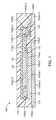
- FIG. 1shows a side cross-sectional view of a semiconductor die package.
- FIG. 2( a )shows a perspective view of a premolded clip structure.
- FIG. 2( b )shows a side schematic view of a semiconductor die comprising a vertical MOSFET.
- FIG. 3shows a perspective view of a semiconductor die package comprising two dice.
- FIG. 4shows a top view of the die package in FIG. 3 .
- FIG. 5shows a portion of the die package in FIG. 3 , without a clip structure.
- FIGS. 6-7show exemplary process flows.
- FIGS. 8-9show portions of a clip structure that can be partially etched.
- FIG. 10shows a semiconductor die package according to another embodiment of the invention.
- Embodiments of the inventionare directed to pre-molded clip structures, methods for making pre-molded clip structures, semiconductor die packages including the pre-molded clip structures, and methods for making the semiconductor die packages.
- the pre-molded clip structures according to embodiments of the inventionallow gate and source connections to be made simultaneously to electrical terminals (e.g., a source terminal and a gate terminal) in a single die or multiple dice, since clips that couple to those terminals are premolded together with a molding material. This can result in more uniform solder connections, since the relative positions of such clips can be fixed and consistent prior to when they are attached to the semiconductor die.
- electrical terminalse.g., a source terminal and a gate terminal
- a pre-molded clip structurecan be made with solderable contact areas defined via a molding process or via a combination of molding and partial-etching (e.g., half-etching) processes to allow compatibility with stamped clip options.
- a partial or half-etching processcan define solderable connection sites at predetermined locations. This can result in optimum RDSon performance and can facilitate the flow of a molding material under a clip connection while improving clip locking within the die package.
- Clip bonding processes using the premolded clip structurecan advantageously use one pick-and-place step to provide connections for a single die or multiple dice.
- the premolded clip structuremay use a 0.203 mm (or larger) sheet of metal (e.g., copper), etched or stamped according to a desired design of the solderable part, and may then be molded.
- the overall thickness of the premolded clip structuremay be around 0.3 mm, or greater.
- a premolded clip structure according to an embodiment of the inventioncan be used in any suitable type of semiconductor die package including a wireless MLP (micro-lead package) structure.
- a clip frameFor a wireless MLP type package, it is also possible to design a clip frame so that it is a high density matrix frame ( ⁇ 400 units per strip for a 70 mm frame width). Hence, it is possible to lower the cost of a clip frame and thereby compensate for any added cost resulting from additional clip molding and sawing processes.
- Another advantage of this conceptis its adaptability for creating multiple chip modules (MCM).
- source and gate clip connectionscan be defined on a frame via a molding process instead of laying out complicated clip designs.
- FIG. 1shows a side, cross-sectional view of a semiconductor die package 100 according to an embodiment of the invention.
- the package 100comprises a semiconductor die 110 which is attached to a leadframe structure 124 , and is a wireless MLP-type package.
- the leadframe structure 124comprises a die attach portion 124 ( a ) (which may be a drain lead structure) comprising a die attach surface 124 ( a )- 1 proximate to the die 110 . It is electrically coupled to a drain in a MOSFET in the die 110 An exterior leadframe surface 124 ( a )- 2 may be opposite to the die attach surface 124 ( a )- 1 .
- the leadframe structure 124also comprises a source lead structure 124 ( b ) including a first end portion 124 ( b )- 1 , an intermediate portion 124 ( b )- 2 , and a second end portion 124 ( b )- 3 . Portions 124 ( b )- 1 , 124 ( b )- 2 , and 124 ( b )- 3 are in a stepped configuration.
- the leadframe structures 124may be made of any suitable conductive material including plated and unplated metals. Suitable materials may include copper.
- the semiconductor die package 100also comprises a premolded clip structure 130 .
- the premolded clip structure 130comprises a first clip 118 and a first molding material 128 around at least a portion of the first clip 118 .
- the first molding material 128may comprise any suitable material including an epoxy molding material.
- the first clip 118 and any other clipsmay be made of any suitable material including copper.
- the first clip 118 and any other clipsmay be plated or unplated.
- the first clip 118may be a source clip and may comprise a first portion 118 ( a ) which is electrically and mechanically coupled to a source region of the semiconductor die 110 using a conductive material 122 (e.g., a conductive adhesive) such as solder or a conductive epoxy, as well as a second portion 118 ( b ), and an intermediate portion 118 ( c ).
- the first portion 118 ( a )may comprise a die attach surface 118 ( a )- 1 and an opposite surface 118 ( a )- 2 .
- the second portion 118 ( b )is mechanically and electrically coupled to the source lead structure 124 using a conductive adhesive 129 such as solder or a conductive epoxy.
- the second portion 118 ( b )may comprise a lead attach surface 118 ( b )- 1 and an opposite surface 118 ( b )- 2 .
- the intermediate portion 118 ( c )is between the first portion 118 ( a ) and the second portion 118 ( b ) of the first clip 118 .
- the intermediate portion 118 ( c )may have been formed by an etching process, and is therefore thinner than the first portion 118 ( a ) and the second portion 118 ( b ) of the first clip 118 .
- the first clip 118has a number of partially etched regions 118 ( d ) (sometimes referred to as “half-etched” when about half of the thickness of the clip is etched away). As shown in FIG. 1 , the molding material 128 fills the regions that were etched away to lock the first clip 118 into the molding material 128 .
- a second molding material 114which may be the same or different than the molding material 128 in the premolded clip structure 130 , may cover some or all of the premolded clip structure 130 , and the semiconductor die 110 .
- the second molding material 114may also cover a portion of the leadframe structure 124 . Because the second molding material 114 and the first molding material 128 are formed in separate processes, an interface may be formed between the first molding material 128 and the second molding material 114 in some embodiments.
- the second molding material 114does not extend beyond the lateral edges of the drain lead structure 124 ( a ) and the source lead structure 124 .
- the packagescould include leads which extend beyond the lateral edges of the second molding material 114 .
- the surface 124 ( a )- 2 and the exterior surface corresponding to the second end portion 124 ( b )- 3are exposed by the second molding material 114 .
- the exposed surfacesmay be mounted to conductive lands on a circuit substrate (not shown) such as a circuit board.
- FIG. 2( a )shows the underside of the premolded clip structure 130 .
- the cross-sectional view of the premolded clip in FIG. 1may be along the line P-P.
- the die attach surface 118 ( a )- 1 of the first clip 118 and the lead attach surface 118 ( b )- 1 of the first clipare exposed through the molding material 128 .
- FIG. 2( a )also shows a die attach surface 136 ( a )- 1 and a lead attach surface 136 ( b )- 1 corresponding to a second clip 136 which may be a gate clip.
- the second clip 136may electrically connect a gate lead in the previously described leadframe structure and a gate region in the previously described die using a conductive adhesive such as solder or a conductive epoxy.
- the second clip 136may also comprise a first portion including the die attach surface 136 ( a )- 1 , a second portion including the lead attach surface 136 ( b )- 1 , and an intermediate portion (covered by the molding material 128 ) that is thinner than the first portion and the second portion.
- the first clip 118 and the second clip 136are separated from each other and are electrically isolated from each other by the molding material 128 .
- the molding material 128binds the first clip 118 and the second clip 136 together so that the first clip 118 and the second clip 136 can be mounted on to a corresponding source region and a corresponding gate region in a semiconductor die together in one step and using vacuum tool element that includes one vacuum hole.
- Thisis unlike conventional processes where separate vacuum holes for a separated first clip and a separated second clip would be needed. Consequently, embodiments of the invention provide for more efficient processing and can also provide for more accurate alignment of the first and second clips 118 , 136 when they are bonded to a semiconductor die, since they already in fixed positions relative to each other during bonding.
- FIG. 2( b )shows a schematic cross-section of a die comprising a vertical power MOSFET.
- the die 110comprising a source region S and a gate region G at one surface of the die 118 , and a drain region D at the opposite surface of the die 110 .
- VDMOS transistorsinclude VDMOS transistors and vertical bipolar transistors.
- a VDMOS transistoris a MOSFET that has two or more semiconductor regions foamed by diffusion. It has a source region, a drain region, and a gate. The device is vertical in that the source region and the drain region are at opposite surfaces of the semiconductor die.
- the gatemay be a trenched gate structure or a planar gate structure, and is formed at the same surface as the source region. Trenched gate structures are preferred, since trenched gate structures are narrower and occupy less space than planar gate structures.
- the current flow from the source region to the drain region in a VDMOS deviceis substantially perpendicular to the die surfaces.
- the semiconductor dicecould alternatively include other vertical devices such as resistors as well as bipolar junction transistors.
- FIG. 3shows a perspective view of a semiconductor die package 200 comprising two dice 210 within a single package.
- the semiconductor die package 200comprises two first clips 218 and two second clips 236 .
- the two first clipsmay be source clips coupled to source regions in the semiconductor dice 210 .
- the two second clips 236may be gate clips coupled to the gate regions in the semiconductor dice 210 .
- the semiconductor dice 210may be mounted on a leadframe structure 224 .
- a first molding material 228may couple the first clips 218 and the second clips 236 together, and they may form a premolded clip structure 230 .
- a second molding materialis not shown in FIG. 3 .
- two dice and two clips per dieare shown in this example, it is understood that embodiments of the invention may include more than two dice and/or more than two clips per dice in other embodiments of the invention.
- FIG. 4shows a top view of the die package 200 shown in FIG. 3 .
- FIG. 5shows a perspective view of the semiconductor die package shown in FIG. 3 , without the premolded clip structure 230 on top for the dice 210 .
- conductive adhesives 228 , 222 ( g ), and 222 ( s )are shown. They may include a conductive adhesive 222 ( g ) on a gate region and a conductive adhesive 222 ( s ) on a source region of the semiconductor die 210 .
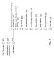
- FIG. 6shows a flowchart illustrating a method according to an embodiment of the invention.
- solder paste(or a solder wire) may be used to attach a semiconductor die to a leadframe structure (step 502 ). Then, solder paste can be dispensed or screen printed on the surface of the semiconductor die opposite the leadframe structure (step 504 ). Then, the previously described premolded clip structure may be attached to the semiconductor die (step 506 ).
- the clip premolding processcan occur using the previously described first molding material and first and second clips.
- the first and second clipsmay be in an array of clips.
- the array of premolded clip structuresmay be separated by sawing or some other process (step 503 ).
- a reflow process and an optional flux cleaning processcan be performed (steps 508 , 510 ).
- a block molding processis performed (step 512 ) using a molding tool.
- a second molding materialis formed around at least a portion of the die, the leadframe structure, and the premolded clip structure (step 512 ).
- strip marking, package sawing, and test processesare performed (steps 514 , 516 , 518 ).
- FIG. 7shows another flowchart illustrating another method according to an embodiment of the invention.
- the steps in FIG. 7 and FIG. 6are the same, except that an additional step of partially etching exposed copper is shown (step 507 ). This additional step can be further described with references to FIGS. 8 and 9 .
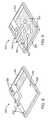
- FIGS. 8 and 9show how copper clips in premolded clip structures 330 including a first molding material 328 can be selectively plated with metallic materials 354 such as noble metals or composite layers comprising noble metals (e.g., NiPdAu).
- metallic materials 354such as noble metals or composite layers comprising noble metals (e.g., NiPdAu).
- the exposed bare copper areas 352will later be partially or half-etched to create specific soldering sites (as in FIG. 8 ) or specific soldering pedestals on the clip (as in FIG. 9 ). These bare copper areas 352 are recessed after etching.
- the plated NiPdAu areas 354will protrude from the bare copper areas 352 after etching.
- the etched copper areas 352can facilitate mold compound flow under the clip structures 330 and can enhance clip locking during the second, block molding process with the second molding material (step 512 in FIGS. 6-7 ).
- FIGS. 8 and 9also show tie bars 350 which form pathways for volatiles that can facilitate the escape of outgas components from solder paste during soldering process.
- FIG. 10shows a side, cross-sectional view of a semiconductor die package like the one shown in FIG. 1 .
- the second molding material 114does not extend beyond the top surface (including surfaces 118 ( a )- 2 , 118 ( b )- 2 ) of the first clip 118 , as well as a corresponding second clip (not shown).
- This top exposed optioncan use a film or tape assisted molding process, where a top and bottom film is placed on areas that will not receive a molding material. The molding process can be used to ensure that molding material does not bleed on to exposed pads.
- the package shown in FIG. 10is thinner, and a heat sink may be placed on top of the premolded clip structure 130 to provide for improved heat dissipation.
- premolded clip structures and semiconductor die packages described abovecan be used in larger modules and systems.
- Such systemsmay include cellular phones, computers, servers, etc.
Landscapes
- Engineering & Computer Science (AREA)
- Computer Hardware Design (AREA)
- Microelectronics & Electronic Packaging (AREA)
- Power Engineering (AREA)
- Physics & Mathematics (AREA)
- Condensed Matter Physics & Semiconductors (AREA)
- General Physics & Mathematics (AREA)
- Structures Or Materials For Encapsulating Or Coating Semiconductor Devices Or Solid State Devices (AREA)
- Shaping Of Tube Ends By Bending Or Straightening (AREA)
- Encapsulation Of And Coatings For Semiconductor Or Solid State Devices (AREA)
- Lead Frames For Integrated Circuits (AREA)
Abstract
Description
Claims (17)
Priority Applications (2)
| Application Number | Priority Date | Filing Date | Title |
|---|---|---|---|
| US12/822,932US8008759B2 (en) | 2007-01-24 | 2010-06-24 | Pre-molded clip structure |
| US13/186,246US8513059B2 (en) | 2007-01-24 | 2011-07-19 | Pre-molded clip structure |
Applications Claiming Priority (2)
| Application Number | Priority Date | Filing Date | Title |
|---|---|---|---|
| US11/626,503US7768105B2 (en) | 2007-01-24 | 2007-01-24 | Pre-molded clip structure |
| US12/822,932US8008759B2 (en) | 2007-01-24 | 2010-06-24 | Pre-molded clip structure |
Related Parent Applications (1)
| Application Number | Title | Priority Date | Filing Date |
|---|---|---|---|
| US11/626,503ContinuationUS7768105B2 (en) | 2007-01-24 | 2007-01-24 | Pre-molded clip structure |
Related Child Applications (1)
| Application Number | Title | Priority Date | Filing Date |
|---|---|---|---|
| US13/186,246DivisionUS8513059B2 (en) | 2007-01-24 | 2011-07-19 | Pre-molded clip structure |
Publications (2)
| Publication Number | Publication Date |
|---|---|
| US20100258924A1 US20100258924A1 (en) | 2010-10-14 |
| US8008759B2true US8008759B2 (en) | 2011-08-30 |
Family
ID=39640437
Family Applications (4)
| Application Number | Title | Priority Date | Filing Date |
|---|---|---|---|
| US11/626,503Active2028-10-24US7768105B2 (en) | 2007-01-24 | 2007-01-24 | Pre-molded clip structure |
| US12/822,675ActiveUS7838340B2 (en) | 2007-01-24 | 2010-06-24 | Pre-molded clip structure |
| US12/822,932ActiveUS8008759B2 (en) | 2007-01-24 | 2010-06-24 | Pre-molded clip structure |
| US13/186,246ActiveUS8513059B2 (en) | 2007-01-24 | 2011-07-19 | Pre-molded clip structure |
Family Applications Before (2)
| Application Number | Title | Priority Date | Filing Date |
|---|---|---|---|
| US11/626,503Active2028-10-24US7768105B2 (en) | 2007-01-24 | 2007-01-24 | Pre-molded clip structure |
| US12/822,675ActiveUS7838340B2 (en) | 2007-01-24 | 2010-06-24 | Pre-molded clip structure |
Family Applications After (1)
| Application Number | Title | Priority Date | Filing Date |
|---|---|---|---|
| US13/186,246ActiveUS8513059B2 (en) | 2007-01-24 | 2011-07-19 | Pre-molded clip structure |
Country Status (6)
| Country | Link |
|---|---|
| US (4) | US7768105B2 (en) |
| CN (1) | CN101595560B (en) |
| DE (1) | DE112008000234T5 (en) |
| MY (2) | MY163758A (en) |
| TW (1) | TWI441299B (en) |
| WO (1) | WO2008091742A2 (en) |
Cited By (2)
| Publication number | Priority date | Publication date | Assignee | Title |
|---|---|---|---|---|
| US20110215460A1 (en)* | 2008-07-15 | 2011-09-08 | Infineon Technologies Ag | Stacked semiconductor chips |
| US9472491B2 (en)* | 2014-09-30 | 2016-10-18 | Alpha And Omega Semiconductor Incorporated | Semiconductor package with small gate clip and assembly method |
Families Citing this family (50)
| Publication number | Priority date | Publication date | Assignee | Title |
|---|---|---|---|---|
| US8106501B2 (en)* | 2008-12-12 | 2012-01-31 | Fairchild Semiconductor Corporation | Semiconductor die package including low stress configuration |
| US7768105B2 (en) | 2007-01-24 | 2010-08-03 | Fairchild Semiconductor Corporation | Pre-molded clip structure |
| US7683463B2 (en)* | 2007-04-19 | 2010-03-23 | Fairchild Semiconductor Corporation | Etched leadframe structure including recesses |
| US7972906B2 (en)* | 2008-03-07 | 2011-07-05 | Fairchild Semiconductor Corporation | Semiconductor die package including exposed connections |
| US7898067B2 (en)* | 2008-10-31 | 2011-03-01 | Fairchild Semiconductor Corporaton | Pre-molded, clip-bonded multi-die semiconductor package |
| US8193618B2 (en) | 2008-12-12 | 2012-06-05 | Fairchild Semiconductor Corporation | Semiconductor die package with clip interconnection |
| US7816784B2 (en)* | 2008-12-17 | 2010-10-19 | Fairchild Semiconductor Corporation | Power quad flat no-lead semiconductor die packages with isolated heat sink for high-voltage, high-power applications, systems using the same, and methods of making the same |
| US20100164078A1 (en)* | 2008-12-31 | 2010-07-01 | Ruben Madrid | Package assembly for semiconductor devices |
| EP2242094A1 (en)* | 2009-04-17 | 2010-10-20 | Nxp B.V. | Foil and method for foil-based bonding and resulting package |
| US8354303B2 (en)* | 2009-09-29 | 2013-01-15 | Texas Instruments Incorporated | Thermally enhanced low parasitic power semiconductor package |
| US20110084332A1 (en)* | 2009-10-08 | 2011-04-14 | Vishay General Semiconductor, Llc. | Trench termination structure |
| US20110095410A1 (en)* | 2009-10-28 | 2011-04-28 | Fairchild Semiconductor Corporation | Wafer level semiconductor device connector |
| US20110095417A1 (en)* | 2009-10-28 | 2011-04-28 | Fairchild Semiconductor Corporation | Leadless semiconductor device terminal |
| CN102842549B (en)* | 2012-08-23 | 2015-12-16 | 苏州固锝电子股份有限公司 | The power MOSFET package body of square flat non-pin |
| CN102842548A (en)* | 2012-08-23 | 2012-12-26 | 苏州固锝电子股份有限公司 | Square flat-type power metal oxide semi-conductor (MOS) chip packaging structure |
| CN102842550B (en)* | 2012-08-23 | 2015-12-16 | 苏州固锝电子股份有限公司 | The DFN encapsulating structure of power mosfet chip |
| JP5970316B2 (en) | 2012-09-26 | 2016-08-17 | ルネサスエレクトロニクス株式会社 | Manufacturing method of semiconductor device |
| US9478484B2 (en) | 2012-10-19 | 2016-10-25 | Infineon Technologies Austria Ag | Semiconductor packages and methods of formation thereof |
| US9070721B2 (en)* | 2013-03-15 | 2015-06-30 | Semiconductor Components Industries, Llc | Semiconductor devices and methods of making the same |
| CN103208474A (en)* | 2013-03-22 | 2013-07-17 | 苏州固锝电子股份有限公司 | Quad flat type high-power chip packing structure |
| US9041170B2 (en)* | 2013-04-02 | 2015-05-26 | Infineon Technologies Austria Ag | Multi-level semiconductor package |
| US9214415B2 (en)* | 2013-04-11 | 2015-12-15 | Texas Instruments Incorporated | Integrating multi-output power converters having vertically stacked semiconductor chips |
| JP6147588B2 (en)* | 2013-07-01 | 2017-06-14 | ルネサスエレクトロニクス株式会社 | Semiconductor device |
| WO2015076960A1 (en)* | 2013-11-21 | 2015-05-28 | United Technologies Corporation | Method to integrate multiple electric circuits into organic matrix composite |
| US9385111B2 (en)* | 2013-11-22 | 2016-07-05 | Infineon Technologies Austria Ag | Electronic component with electronic chip between redistribution structure and mounting structure |
| JP2015142072A (en) | 2014-01-30 | 2015-08-03 | 株式会社東芝 | semiconductor device |
| JP6338937B2 (en) | 2014-06-13 | 2018-06-06 | ローム株式会社 | Power module and manufacturing method thereof |
| US10796986B2 (en)* | 2016-03-21 | 2020-10-06 | Infineon Technologies Ag | Leadframe leads having fully plated end faces |
| TWM544108U (en)* | 2017-01-20 | 2017-06-21 | Taiwan Semiconductor Co Ltd | Integrated package structure |
| US10121742B2 (en)* | 2017-03-15 | 2018-11-06 | Amkor Technology, Inc. | Method of forming a packaged semiconductor device using ganged conductive connective assembly and structure |
| DE112018002151T5 (en)* | 2017-03-28 | 2020-01-16 | Rohm Co., Ltd. | SEMICONDUCTOR DEVICE AND METHOD FOR PRODUCING A SEMICONDUCTOR DEVICE |
| US10727151B2 (en)* | 2017-05-25 | 2020-07-28 | Infineon Technologies Ag | Semiconductor chip package having a cooling surface and method of manufacturing a semiconductor package |
| KR20190071111A (en)* | 2017-12-14 | 2019-06-24 | 삼성전자주식회사 | An apparatus for x-ray inspection, and a method for manufacturing a semiconductor device using the same |
| US11088046B2 (en) | 2018-06-25 | 2021-08-10 | Semiconductor Components Industries, Llc | Semiconductor device package with clip interconnect and dual side cooling |
| IT201800020998A1 (en) | 2018-12-24 | 2020-06-24 | St Microelectronics Srl | Process for manufacturing semiconductor devices and corresponding semiconductor device |
| US10964629B2 (en) | 2019-01-18 | 2021-03-30 | Texas Instruments Incorporated | Siderail with mold compound relief |
| CN110211887A (en)* | 2019-06-11 | 2019-09-06 | 山东海声尼克微电子有限公司 | A kind of lock material hole copper sheet welding procedure for large-current electric source module wire bonding |
| CN110190004A (en)* | 2019-06-11 | 2019-08-30 | 山东海声尼克微电子有限公司 | A kind of welding procedure for high-current supply Module bond |
| CN110416101A (en)* | 2019-08-07 | 2019-11-05 | 深圳市顺益微电子有限公司 | Use sintering silver paste as the power module copper sheet welding procedure of bonding agent |
| US11158567B2 (en) | 2019-08-09 | 2021-10-26 | Texas Instruments Incorporated | Package with stacked power stage and integrated control die |
| US11715679B2 (en) | 2019-10-09 | 2023-08-01 | Texas Instruments Incorporated | Power stage package including flexible circuit and stacked die |
| US11302615B2 (en) | 2019-12-30 | 2022-04-12 | Texas Instruments Incorporated | Semiconductor package with isolated heat spreader |
| CN113496960A (en)* | 2020-04-01 | 2021-10-12 | 上海凯虹科技电子有限公司 | Package and packaging method |
| US11239127B2 (en)* | 2020-06-19 | 2022-02-01 | Infineon Technologies Ag | Topside-cooled semiconductor package with molded standoff |
| TWI727861B (en)* | 2020-07-23 | 2021-05-11 | 朋程科技股份有限公司 | Chip packaging structure and method of manufacturing the same |
| US20220208716A1 (en)* | 2020-12-31 | 2022-06-30 | UTAC Headquarters Pte. Ltd. | Semiconductor Device and Method of Forming Clip Bond Having Multiple Bond Line Thicknesses |
| US11652078B2 (en) | 2021-04-20 | 2023-05-16 | Infineon Technologies Ag | High voltage semiconductor package with pin fit leads |
| IT202200001646A1 (en)* | 2022-02-01 | 2023-08-01 | St Microelectronics Srl | Process for manufacturing semiconductor devices and corresponding semiconductor device |
| KR20230131024A (en)* | 2022-03-04 | 2023-09-12 | 현대자동차주식회사 | Power module for vehicle and manufacturing method the same |
| IT202200022431A1 (en)* | 2022-11-02 | 2024-05-02 | St Microelectronics Srl | Process for manufacturing semiconductor devices, component, semiconductor device and corresponding process |
Citations (65)
| Publication number | Priority date | Publication date | Assignee | Title |
|---|---|---|---|---|
| US5821615A (en) | 1995-12-06 | 1998-10-13 | Lg Semicon Co., Ltd. | Semiconductor chip package having clip-type outlead and fabrication method of same |
| US6307755B1 (en) | 1999-05-27 | 2001-10-23 | Richard K. Williams | Surface mount semiconductor package, die-leadframe combination and leadframe therefor and method of mounting leadframes to surfaces of semiconductor die |
| US6329706B1 (en) | 1999-08-24 | 2001-12-11 | Fairchild Korea Semiconductor, Ltd. | Leadframe using chip pad as heat conducting path and semiconductor package adopting the same |
| US20010052639A1 (en) | 2000-06-13 | 2001-12-20 | Fairchild Korea Semiconductor Ltd. | Power module package having insulator type heat sink attached to rear surface of lead frame and manufacturing method thereof |
| US20020057553A1 (en) | 2000-11-10 | 2002-05-16 | Fairchild Korea Semiconductor Ltd. | Stacked intelligent power module package |
| US20020066950A1 (en) | 2000-12-04 | 2002-06-06 | Fairchild Semiconductor Corporation | Flip chip in leaded molded package with two dies |
| US6424035B1 (en) | 1998-11-05 | 2002-07-23 | Fairchild Semiconductor Corporation | Semiconductor bilateral switch |
| US6423623B1 (en) | 1998-06-09 | 2002-07-23 | Fairchild Semiconductor Corporation | Low Resistance package for semiconductor devices |
| US6449174B1 (en) | 2001-08-06 | 2002-09-10 | Fairchild Semiconductor Corporation | Current sharing in a multi-phase power supply by phase temperature control |
| US20020140070A1 (en) | 2001-03-30 | 2002-10-03 | Fairchild Semiconductor Corp. | Packaging system for die-up connection of a die-down oriented integrated circuit |
| US6465276B2 (en)* | 2000-05-18 | 2002-10-15 | Siliconx (Taiwan) Ltd. | Power semiconductor package and method for making the same |
| US20020175383A1 (en) | 2000-12-06 | 2002-11-28 | Fairchild Semiconductor Corporation | MOS-gated power device with doped polysilicon body and process for forming same |
| US6489678B1 (en) | 1998-08-05 | 2002-12-03 | Fairchild Semiconductor Corporation | High performance multi-chip flip chip package |
| US20030014620A1 (en) | 1998-10-30 | 2003-01-16 | Fairchild Semiconductor Corporation | Method and circuit for performing automatic power on reset of an integrated circuit |
| US20030011054A1 (en) | 2001-06-11 | 2003-01-16 | Fairchild Semiconductor Corporation | Power module package having improved heat dissipating capability |
| US20030011005A1 (en) | 2001-02-01 | 2003-01-16 | Fairchild Semiconductor Corporation | Unmolded package for a semiconductor device |
| US20030025183A1 (en) | 2001-08-01 | 2003-02-06 | Fairchild Semiconductor Corporation | Packaged semiconductor device and method of manufacture using shaped die |
| US20030042403A1 (en) | 2001-08-31 | 2003-03-06 | Fairchild Semiconductor Corporation | Surface mountable optocoupler package |
| US20030052408A1 (en) | 2000-04-13 | 2003-03-20 | Fairchild Semiconductor Corporation | Semiconductor device including molded wireless exposed drain packaging |
| US20030067065A1 (en) | 2001-09-17 | 2003-04-10 | Fairchild Korea Semiconductor Ltd. | Three-dimensional power semiconductor module and method of manufacturing the same |
| US20030075786A1 (en) | 2001-10-22 | 2003-04-24 | Fairchild Semiconductor Corporation | Thin, thermally enhanced flip chip in a leaded molded package |
| US6556750B2 (en) | 2000-05-26 | 2003-04-29 | Fairchild Semiconductor Corporation | Bi-directional optical coupler |
| US6556749B2 (en) | 1999-12-09 | 2003-04-29 | Hitachi Cable Limited | Array waveguide grating and method of manufacture thereof |
| US20030085464A1 (en) | 2001-11-02 | 2003-05-08 | Fairchild Semiconductor Corporation | Semiconductor packages for semiconductor devices |
| US20030085456A1 (en) | 2001-10-05 | 2003-05-08 | Fairchild Semiconductor Corporation | Semiconductor power package module |
| US20030139020A1 (en) | 2002-01-22 | 2003-07-24 | Fairchild Semiconductor Corporation | Semiconductor die package with semiconductor die having side electrical connection |
| US6621152B2 (en) | 2000-12-19 | 2003-09-16 | Fairchild Korea Semiconductor Ltd. | Thin, small-sized power semiconductor package |
| US20030173659A1 (en) | 2002-03-14 | 2003-09-18 | Fairchild Korea Semiconductor Ltd. | Semiconductor package having oxidation-free copper wire |
| US20030178717A1 (en) | 2000-11-16 | 2003-09-25 | Fairchild Semiconductor Corporation | Flip chip with solder pre-plated leadframe including locating holes |
| US6630726B1 (en) | 2001-11-07 | 2003-10-07 | Amkor Technology, Inc. | Power semiconductor package with strap |
| US6645791B2 (en) | 2001-04-23 | 2003-11-11 | Fairchild Semiconductor | Semiconductor die package including carrier with mask |
| US6677672B2 (en)* | 2002-04-26 | 2004-01-13 | Semiconductor Components Industries Llc | Structure and method of forming a multiple leadframe semiconductor device |
| US6683375B2 (en) | 2001-06-15 | 2004-01-27 | Fairchild Semiconductor Corporation | Semiconductor die including conductive columns |
| US20040041242A1 (en) | 2002-08-30 | 2004-03-04 | Fairchild Semiconductor Corporation | Substrate based unmolded package including lead frame structure and semiconductor die |
| US20040056364A1 (en) | 1999-12-16 | 2004-03-25 | Fairchild Semiconductor Corporation | Flip chip in leaded molded package and method of manufacture thereof |
| US20040063240A1 (en) | 2002-09-30 | 2004-04-01 | Fairchild Semiconductor Corporation | Semiconductor die package including drain clip |
| US6731003B2 (en) | 2002-03-12 | 2004-05-04 | Fairchild Semiconductor Corporation | Wafer-level coated copper stud bumps |
| US6756689B2 (en) | 1999-09-13 | 2004-06-29 | Fairchild Korea Semiconductor, Ltd. | Power device having multi-chip package structure |
| US20040125573A1 (en) | 2002-12-26 | 2004-07-01 | Fairchild Semiconductor Corporation | Multichip module including substrate with an array of interconnect structures |
| US20040130011A1 (en) | 2001-05-15 | 2004-07-08 | Fairchild Semiconductor Corporation | Power chip scale package |
| US20040157372A1 (en)* | 2003-02-11 | 2004-08-12 | Manatad Romel N. | Alternative flip chip in leaded molded package design and method for manufacture |
| US20040232542A1 (en) | 2001-05-14 | 2004-11-25 | Fairchild Semiconductor Corporation | Carrier with metal bumps for semiconductor die packages |
| US6836023B2 (en) | 2002-04-17 | 2004-12-28 | Fairchild Semiconductor Corporation | Structure of integrated trace of chip package |
| US20050001293A1 (en) | 2001-03-12 | 2005-01-06 | Fairchild Semiconductor Corporation | Method for forming semiconductor device including stacked dies |
| US6853064B2 (en)* | 2003-05-12 | 2005-02-08 | Micron Technology, Inc. | Semiconductor component having stacked, encapsulated dice |
| US20050051878A1 (en) | 2000-07-19 | 2005-03-10 | Fairchild Semiconductor Corporation | Flip chip substrate design |
| US6867489B1 (en) | 2002-01-22 | 2005-03-15 | Fairchild Semiconductor Corporation | Semiconductor die package processable at the wafer level |
| US6867481B2 (en) | 2003-04-11 | 2005-03-15 | Fairchild Semiconductor Corporation | Lead frame structure with aperture or groove for flip chip in a leaded molded package |
| US20050167742A1 (en) | 2001-01-30 | 2005-08-04 | Fairchild Semiconductor Corp. | Power semiconductor devices and methods of manufacture |
| US6943434B2 (en) | 2002-10-03 | 2005-09-13 | Fairchild Semiconductor Corporation | Method for maintaining solder thickness in flipchip attach packaging processes |
| US20060113646A1 (en)* | 2004-11-30 | 2006-06-01 | Eswarappa Channabasappa | Connection arrangement for micro lead frame plastic packages |
| US7122884B2 (en) | 2002-04-16 | 2006-10-17 | Fairchild Semiconductor Corporation | Robust leaded molded packages and methods for forming the same |
| US20070001278A1 (en) | 2005-06-30 | 2007-01-04 | Oseob Jeon | Semiconductor die package and method for making the same |
| US20070034994A1 (en) | 2005-06-27 | 2007-02-15 | Fairchild Korea Semiconductor, Ltd. | Package frame and semiconductor package using the same |
| US7196313B2 (en) | 2004-04-02 | 2007-03-27 | Fairchild Semiconductor Corporation | Surface mount multi-channel optocoupler |
| US7199461B2 (en) | 2003-01-21 | 2007-04-03 | Fairchild Korea Semiconductor, Ltd | Semiconductor package suitable for high voltage applications |
| US7242076B2 (en) | 2004-05-18 | 2007-07-10 | Fairchild Semiconductor Corporation | Packaged integrated circuit with MLP leadframe and method of making same |
| US7256479B2 (en) | 2005-01-13 | 2007-08-14 | Fairchild Semiconductor Corporation | Method to manufacture a universal footprint for a package with exposed chip |
| US20070205503A1 (en) | 2006-03-03 | 2007-09-06 | Fairchild Korea Semiconductor, Ltd. | Package and package assembly of power device |
| US7268414B2 (en) | 2002-05-10 | 2007-09-11 | Fairchild Korea Semiconductor Ltd. | Semiconductor package having solder joint of improved reliability |
| US7271497B2 (en) | 2003-03-10 | 2007-09-18 | Fairchild Semiconductor Corporation | Dual metal stud bumping for flip chip applications |
| US7285849B2 (en) | 2005-11-18 | 2007-10-23 | Fairchild Semiconductor Corporation | Semiconductor die package using leadframe and clip and method of manufacturing |
| US20080173991A1 (en)* | 2007-01-24 | 2008-07-24 | Erwin Victor Cruz | Pre-molded clip structure |
| US20090057855A1 (en) | 2007-08-30 | 2009-03-05 | Maria Clemens Quinones | Semiconductor die package including stand off structures |
| US20100109134A1 (en) | 2008-10-31 | 2010-05-06 | Jereza Armand Vincent C | Pre-molded, clip-bonded multi-die semiconductor package |
Family Cites Families (24)
| Publication number | Priority date | Publication date | Assignee | Title |
|---|---|---|---|---|
| US2256493A (en)* | 1934-04-13 | 1941-09-23 | Budd Edward G Mfg Co | Rail car front end construction |
| US2148078A (en)* | 1935-09-26 | 1939-02-21 | New York Central Railroad Co | Streamline locomotive and tender |
| US2108203A (en)* | 1935-09-26 | 1938-02-15 | New York Central Railroad Co | Streamlined locomotive and tender and vestibule curtain structure therefor |
| US3934922A (en)* | 1974-09-05 | 1976-01-27 | Aerovironment Inc. | Aerodynamic drag reduction devices for surface vehicles |
| US4257640A (en)* | 1975-12-16 | 1981-03-24 | Rudkin-Wiley Corporation | Drag reducer for land vehicles |
| US4030779A (en)* | 1976-03-18 | 1977-06-21 | Johnson David W | Inflatable streamlining structure for vehicles |
| US4210354A (en)* | 1978-02-06 | 1980-07-01 | Canning Robert B | Aerodynamic drag-reducing shield for mounting on the front of a cargo carrying compartment of a road vehicle |
| FR2467132B1 (en)* | 1979-10-08 | 1985-08-16 | Levassor Jean | ANTI-WET DEVICE FOR A TRACTOR VEHICLE |
| US4441751A (en)* | 1980-11-24 | 1984-04-10 | Wesley William M | Collapsible high speed extension for motor vehicles |
| US4738203A (en)* | 1984-02-27 | 1988-04-19 | Pullman Standard, Inc. | Aerodynamically structured railway car with corner, air flow guides |
| US4746160A (en)* | 1986-06-30 | 1988-05-24 | Wiesemeyer Robert L | Streamlined truck with semitrailer |
| US4756256A (en)* | 1986-07-30 | 1988-07-12 | Gunderson, Inc. | Aerodynamic drag reduction for railcars |
| US4909154A (en)* | 1989-02-27 | 1990-03-20 | Aero Transportation Products, Inc. | Aerodynamic end closures for railway hopper cars |
| US5222438A (en)* | 1992-07-17 | 1993-06-29 | Grumman Aerospace Corporation | Aerodynamic fairing/brake for high-speed trains |
| US6286894B1 (en)* | 1999-08-10 | 2001-09-11 | D. James Kingham | Reduced-drag trailer |
| US6566749B1 (en)* | 2002-01-15 | 2003-05-20 | Fairchild Semiconductor Corporation | Semiconductor die package with improved thermal and electrical performance |
| US7017508B2 (en)* | 2002-07-12 | 2006-03-28 | Arthur Vanmoor | Hydrodynamically and aerodynamically optimized leading and trailing edge configurations |
| US7073845B2 (en)* | 2003-05-30 | 2006-07-11 | The Regents Of The University Of California | Aerodynamic drag reduction apparatus for gap-divided bluff bodies such as tractor-trailers |
| US7341810B2 (en)* | 2003-09-17 | 2008-03-11 | Ricoh Company, Ltd. | Electrophotographic photoreceptor method of manufacturing electrophotographic photoreceptor, and electrophotographic apparatus and process cartridge using electrophotographic photoreceptor |
| US6972913B2 (en)* | 2004-01-29 | 2005-12-06 | Hewlett-Packard Development Company, L.P. | Two axis tip-tilt platform |
| US7008005B1 (en)* | 2004-09-07 | 2006-03-07 | Freight Wing Inc. | Device for reducing vehicle aerodynamic resistance |
| US7207620B2 (en)* | 2005-08-23 | 2007-04-24 | Cosgrove William E | Aerodynamic drag reducing system with retrofittable, selectively removable frame |
| CN101356633B (en)* | 2005-11-01 | 2011-03-23 | Nxp股份有限公司 | Method for packaging semiconductor die and die package formed by the method |
| US8222718B2 (en)* | 2009-02-05 | 2012-07-17 | Fairchild Semiconductor Corporation | Semiconductor die package and method for making the same |
- 2007
- 2007-01-24USUS11/626,503patent/US7768105B2/enactiveActive
- 2008
- 2008-01-10WOPCT/US2008/050753patent/WO2008091742A2/enactiveApplication Filing
- 2008-01-10MYMYPI2012005163Apatent/MY163758A/enunknown
- 2008-01-10CNCN2008800028902Apatent/CN101595560B/ennot_activeExpired - Fee Related
- 2008-01-10MYMYPI20093078Apatent/MY149108A/enunknown
- 2008-01-10DEDE112008000234Tpatent/DE112008000234T5/ennot_activeWithdrawn
- 2008-01-18TWTW097101986Apatent/TWI441299B/enactive
- 2010
- 2010-06-24USUS12/822,675patent/US7838340B2/enactiveActive
- 2010-06-24USUS12/822,932patent/US8008759B2/enactiveActive
- 2011
- 2011-07-19USUS13/186,246patent/US8513059B2/enactiveActive
Patent Citations (102)
| Publication number | Priority date | Publication date | Assignee | Title |
|---|---|---|---|---|
| US5821615A (en) | 1995-12-06 | 1998-10-13 | Lg Semicon Co., Ltd. | Semiconductor chip package having clip-type outlead and fabrication method of same |
| US6423623B1 (en) | 1998-06-09 | 2002-07-23 | Fairchild Semiconductor Corporation | Low Resistance package for semiconductor devices |
| US6489678B1 (en) | 1998-08-05 | 2002-12-03 | Fairchild Semiconductor Corporation | High performance multi-chip flip chip package |
| US20040159939A1 (en) | 1998-08-05 | 2004-08-19 | Fairchild Semiconductor Corporation | High performance multi-chip flip chip package |
| US6992384B2 (en) | 1998-08-05 | 2006-01-31 | Fairchild Semiconductor Corporation | High performance multi-chip flip chip package |
| US6696321B2 (en) | 1998-08-05 | 2004-02-24 | Fairchild Semiconductor, Corporation | High performance multi-chip flip chip package |
| US6627991B1 (en) | 1998-08-05 | 2003-09-30 | Fairchild Semiconductor Corporation | High performance multi-chip flip package |
| US20030122247A1 (en) | 1998-08-05 | 2003-07-03 | Fairchild Semiconductor Corporation | High performance multi-chip flip chip package |
| US20030107126A1 (en) | 1998-08-05 | 2003-06-12 | Fairchild Semiconductor Corporation | High performance multi-chip flip chip package |
| US20030014620A1 (en) | 1998-10-30 | 2003-01-16 | Fairchild Semiconductor Corporation | Method and circuit for performing automatic power on reset of an integrated circuit |
| US6424035B1 (en) | 1998-11-05 | 2002-07-23 | Fairchild Semiconductor Corporation | Semiconductor bilateral switch |
| US6307755B1 (en) | 1999-05-27 | 2001-10-23 | Richard K. Williams | Surface mount semiconductor package, die-leadframe combination and leadframe therefor and method of mounting leadframes to surfaces of semiconductor die |
| US6329706B1 (en) | 1999-08-24 | 2001-12-11 | Fairchild Korea Semiconductor, Ltd. | Leadframe using chip pad as heat conducting path and semiconductor package adopting the same |
| US6756689B2 (en) | 1999-09-13 | 2004-06-29 | Fairchild Korea Semiconductor, Ltd. | Power device having multi-chip package structure |
| US6556749B2 (en) | 1999-12-09 | 2003-04-29 | Hitachi Cable Limited | Array waveguide grating and method of manufacture thereof |
| US7154168B2 (en) | 1999-12-16 | 2006-12-26 | Fairchild Semiconductor Corporation | Flip chip in leaded molded package and method of manufacture thereof |
| US20050167848A1 (en) | 1999-12-16 | 2005-08-04 | Fairchild Semiconductor Corporation | Filp chip in leaded molded package and method of manufacture thereof |
| US6720642B1 (en) | 1999-12-16 | 2004-04-13 | Fairchild Semiconductor Corporation | Flip chip in leaded molded package and method of manufacture thereof |
| US20040056364A1 (en) | 1999-12-16 | 2004-03-25 | Fairchild Semiconductor Corporation | Flip chip in leaded molded package and method of manufacture thereof |
| US7215011B2 (en) | 1999-12-16 | 2007-05-08 | Fairchild Semiconductor Corporation | Flip chip in leaded molded package and method of manufacture thereof |
| US6989588B2 (en) | 2000-04-13 | 2006-01-24 | Fairchild Semiconductor Corporation | Semiconductor device including molded wireless exposed drain packaging |
| US20030052408A1 (en) | 2000-04-13 | 2003-03-20 | Fairchild Semiconductor Corporation | Semiconductor device including molded wireless exposed drain packaging |
| US6465276B2 (en)* | 2000-05-18 | 2002-10-15 | Siliconx (Taiwan) Ltd. | Power semiconductor package and method for making the same |
| US6556750B2 (en) | 2000-05-26 | 2003-04-29 | Fairchild Semiconductor Corporation | Bi-directional optical coupler |
| US20010052639A1 (en) | 2000-06-13 | 2001-12-20 | Fairchild Korea Semiconductor Ltd. | Power module package having insulator type heat sink attached to rear surface of lead frame and manufacturing method thereof |
| US6432750B2 (en) | 2000-06-13 | 2002-08-13 | Fairchild Korea Semiconductor Ltd. | Power module package having insulator type heat sink attached to rear surface of lead frame and manufacturing method thereof |
| US20050051878A1 (en) | 2000-07-19 | 2005-03-10 | Fairchild Semiconductor Corporation | Flip chip substrate design |
| US20020057553A1 (en) | 2000-11-10 | 2002-05-16 | Fairchild Korea Semiconductor Ltd. | Stacked intelligent power module package |
| US6574107B2 (en) | 2000-11-10 | 2003-06-03 | Fairchild Korea Semiconductor Ltd. | Stacked intelligent power module package |
| US20030178717A1 (en) | 2000-11-16 | 2003-09-25 | Fairchild Semiconductor Corporation | Flip chip with solder pre-plated leadframe including locating holes |
| US20020066950A1 (en) | 2000-12-04 | 2002-06-06 | Fairchild Semiconductor Corporation | Flip chip in leaded molded package with two dies |
| US20040201086A1 (en) | 2000-12-04 | 2004-10-14 | Fairchild Semiconductor Corporation | Flip chip in leaded molded package with two dies |
| US20020175383A1 (en) | 2000-12-06 | 2002-11-28 | Fairchild Semiconductor Corporation | MOS-gated power device with doped polysilicon body and process for forming same |
| US6621152B2 (en) | 2000-12-19 | 2003-09-16 | Fairchild Korea Semiconductor Ltd. | Thin, small-sized power semiconductor package |
| US20050167742A1 (en) | 2001-01-30 | 2005-08-04 | Fairchild Semiconductor Corp. | Power semiconductor devices and methods of manufacture |
| US20030011005A1 (en) | 2001-02-01 | 2003-01-16 | Fairchild Semiconductor Corporation | Unmolded package for a semiconductor device |
| US20040164386A1 (en) | 2001-02-01 | 2004-08-26 | Fairchild Semiconductor Corporation | Unmolded package for a semiconductor device |
| US6740541B2 (en) | 2001-02-01 | 2004-05-25 | Fairchild Semiconductor Corporation | Unmolded package for a semiconductor device |
| US20050001293A1 (en) | 2001-03-12 | 2005-01-06 | Fairchild Semiconductor Corporation | Method for forming semiconductor device including stacked dies |
| US20020140070A1 (en) | 2001-03-30 | 2002-10-03 | Fairchild Semiconductor Corp. | Packaging system for die-up connection of a die-down oriented integrated circuit |
| US6891257B2 (en) | 2001-03-30 | 2005-05-10 | Fairchild Semiconductor Corporation | Packaging system for die-up connection of a die-down oriented integrated circuit |
| US6645791B2 (en) | 2001-04-23 | 2003-11-11 | Fairchild Semiconductor | Semiconductor die package including carrier with mask |
| US7157799B2 (en) | 2001-04-23 | 2007-01-02 | Fairchild Semiconductor Corporation | Semiconductor die package including carrier with mask and semiconductor die |
| US7023077B2 (en) | 2001-05-14 | 2006-04-04 | Fairchild Semiconductor Corporation | Carrier with metal bumps for semiconductor die packages |
| US6893901B2 (en) | 2001-05-14 | 2005-05-17 | Fairchild Semiconductor Corporation | Carrier with metal bumps for semiconductor die packages |
| US20040232542A1 (en) | 2001-05-14 | 2004-11-25 | Fairchild Semiconductor Corporation | Carrier with metal bumps for semiconductor die packages |
| US20040130011A1 (en) | 2001-05-15 | 2004-07-08 | Fairchild Semiconductor Corporation | Power chip scale package |
| US7208819B2 (en) | 2001-06-11 | 2007-04-24 | Fairchild Korea Semiconductor Ltd. | Power module package having improved heat dissipating capability |
| US20030011054A1 (en) | 2001-06-11 | 2003-01-16 | Fairchild Semiconductor Corporation | Power module package having improved heat dissipating capability |
| US20050056918A1 (en) | 2001-06-11 | 2005-03-17 | Fairchild Korea Semiconductor Ltd. | Power module package having improved heat dissipating capability |
| US7061080B2 (en) | 2001-06-11 | 2006-06-13 | Fairchild Korea Semiconductor Ltd. | Power module package having improved heat dissipating capability |
| US20040137724A1 (en) | 2001-06-15 | 2004-07-15 | Fairchild Semiconductor Corporation | Semiconductor die including conductive columns |
| US6683375B2 (en) | 2001-06-15 | 2004-01-27 | Fairchild Semiconductor Corporation | Semiconductor die including conductive columns |
| US7022548B2 (en) | 2001-06-15 | 2006-04-04 | Fairchild Semiconductor Corporation | Method for making a semiconductor die package |
| US20030025183A1 (en) | 2001-08-01 | 2003-02-06 | Fairchild Semiconductor Corporation | Packaged semiconductor device and method of manufacture using shaped die |
| US6449174B1 (en) | 2001-08-06 | 2002-09-10 | Fairchild Semiconductor Corporation | Current sharing in a multi-phase power supply by phase temperature control |
| US20030042403A1 (en) | 2001-08-31 | 2003-03-06 | Fairchild Semiconductor Corporation | Surface mountable optocoupler package |
| US20030067065A1 (en) | 2001-09-17 | 2003-04-10 | Fairchild Korea Semiconductor Ltd. | Three-dimensional power semiconductor module and method of manufacturing the same |
| US20030085456A1 (en) | 2001-10-05 | 2003-05-08 | Fairchild Semiconductor Corporation | Semiconductor power package module |
| US6774465B2 (en) | 2001-10-05 | 2004-08-10 | Fairchild Korea Semiconductor, Ltd. | Semiconductor power package module |
| US6891256B2 (en) | 2001-10-22 | 2005-05-10 | Fairchild Semiconductor Corporation | Thin, thermally enhanced flip chip in a leaded molded package |
| US20030075786A1 (en) | 2001-10-22 | 2003-04-24 | Fairchild Semiconductor Corporation | Thin, thermally enhanced flip chip in a leaded molded package |
| US6674157B2 (en) | 2001-11-02 | 2004-01-06 | Fairchild Semiconductor Corporation | Semiconductor package comprising vertical power transistor |
| US20030085464A1 (en) | 2001-11-02 | 2003-05-08 | Fairchild Semiconductor Corporation | Semiconductor packages for semiconductor devices |
| US6630726B1 (en) | 2001-11-07 | 2003-10-07 | Amkor Technology, Inc. | Power semiconductor package with strap |
| US6867489B1 (en) | 2002-01-22 | 2005-03-15 | Fairchild Semiconductor Corporation | Semiconductor die package processable at the wafer level |
| US20030139020A1 (en) | 2002-01-22 | 2003-07-24 | Fairchild Semiconductor Corporation | Semiconductor die package with semiconductor die having side electrical connection |
| US6830959B2 (en) | 2002-01-22 | 2004-12-14 | Fairchild Semiconductor Corporation | Semiconductor die package with semiconductor die having side electrical connection |
| US6731003B2 (en) | 2002-03-12 | 2004-05-04 | Fairchild Semiconductor Corporation | Wafer-level coated copper stud bumps |
| US20030173659A1 (en) | 2002-03-14 | 2003-09-18 | Fairchild Korea Semiconductor Ltd. | Semiconductor package having oxidation-free copper wire |
| US7122884B2 (en) | 2002-04-16 | 2006-10-17 | Fairchild Semiconductor Corporation | Robust leaded molded packages and methods for forming the same |
| US6836023B2 (en) | 2002-04-17 | 2004-12-28 | Fairchild Semiconductor Corporation | Structure of integrated trace of chip package |
| US6677672B2 (en)* | 2002-04-26 | 2004-01-13 | Semiconductor Components Industries Llc | Structure and method of forming a multiple leadframe semiconductor device |
| US7268414B2 (en) | 2002-05-10 | 2007-09-11 | Fairchild Korea Semiconductor Ltd. | Semiconductor package having solder joint of improved reliability |
| US7061077B2 (en) | 2002-08-30 | 2006-06-13 | Fairchild Semiconductor Corporation | Substrate based unmolded package including lead frame structure and semiconductor die |
| US20040041242A1 (en) | 2002-08-30 | 2004-03-04 | Fairchild Semiconductor Corporation | Substrate based unmolded package including lead frame structure and semiconductor die |
| US6777800B2 (en)* | 2002-09-30 | 2004-08-17 | Fairchild Semiconductor Corporation | Semiconductor die package including drain clip |
| US20040063240A1 (en) | 2002-09-30 | 2004-04-01 | Fairchild Semiconductor Corporation | Semiconductor die package including drain clip |
| US6943434B2 (en) | 2002-10-03 | 2005-09-13 | Fairchild Semiconductor Corporation | Method for maintaining solder thickness in flipchip attach packaging processes |
| US20040125573A1 (en) | 2002-12-26 | 2004-07-01 | Fairchild Semiconductor Corporation | Multichip module including substrate with an array of interconnect structures |
| US6806580B2 (en) | 2002-12-26 | 2004-10-19 | Fairchild Semiconductor Corporation | Multichip module including substrate with an array of interconnect structures |
| US7199461B2 (en) | 2003-01-21 | 2007-04-03 | Fairchild Korea Semiconductor, Ltd | Semiconductor package suitable for high voltage applications |
| US20070181984A1 (en) | 2003-01-21 | 2007-08-09 | Fairchild Korea Semiconductor, Ltd. | Semiconductor package suitable for high voltage applications |
| US7217594B2 (en) | 2003-02-11 | 2007-05-15 | Fairchild Semiconductor Corporation | Alternative flip chip in leaded molded package design and method for manufacture |
| US20040157372A1 (en)* | 2003-02-11 | 2004-08-12 | Manatad Romel N. | Alternative flip chip in leaded molded package design and method for manufacture |
| US7271497B2 (en) | 2003-03-10 | 2007-09-18 | Fairchild Semiconductor Corporation | Dual metal stud bumping for flip chip applications |
| US7081666B2 (en) | 2003-04-11 | 2006-07-25 | Fairchild Semiconductor Corporation | Lead frame structure with aperture or groove for flip chip in a leaded molded package |
| US6867481B2 (en) | 2003-04-11 | 2005-03-15 | Fairchild Semiconductor Corporation | Lead frame structure with aperture or groove for flip chip in a leaded molded package |
| US6853064B2 (en)* | 2003-05-12 | 2005-02-08 | Micron Technology, Inc. | Semiconductor component having stacked, encapsulated dice |
| US7196313B2 (en) | 2004-04-02 | 2007-03-27 | Fairchild Semiconductor Corporation | Surface mount multi-channel optocoupler |
| US7242076B2 (en) | 2004-05-18 | 2007-07-10 | Fairchild Semiconductor Corporation | Packaged integrated circuit with MLP leadframe and method of making same |
| US20060113646A1 (en)* | 2004-11-30 | 2006-06-01 | Eswarappa Channabasappa | Connection arrangement for micro lead frame plastic packages |
| US7256479B2 (en) | 2005-01-13 | 2007-08-14 | Fairchild Semiconductor Corporation | Method to manufacture a universal footprint for a package with exposed chip |
| US20070034994A1 (en) | 2005-06-27 | 2007-02-15 | Fairchild Korea Semiconductor, Ltd. | Package frame and semiconductor package using the same |
| US20070001278A1 (en) | 2005-06-30 | 2007-01-04 | Oseob Jeon | Semiconductor die package and method for making the same |
| US7285849B2 (en) | 2005-11-18 | 2007-10-23 | Fairchild Semiconductor Corporation | Semiconductor die package using leadframe and clip and method of manufacturing |
| US20070205503A1 (en) | 2006-03-03 | 2007-09-06 | Fairchild Korea Semiconductor, Ltd. | Package and package assembly of power device |
| US20080173991A1 (en)* | 2007-01-24 | 2008-07-24 | Erwin Victor Cruz | Pre-molded clip structure |
| US20100258923A1 (en)* | 2007-01-24 | 2010-10-14 | Erwin Victor Cruz | Pre-molded clip structure |
| US7838340B2 (en)* | 2007-01-24 | 2010-11-23 | Fairchild Semiconductor Corporation | Pre-molded clip structure |
| US20090057855A1 (en) | 2007-08-30 | 2009-03-05 | Maria Clemens Quinones | Semiconductor die package including stand off structures |
| US20100109134A1 (en) | 2008-10-31 | 2010-05-06 | Jereza Armand Vincent C | Pre-molded, clip-bonded multi-die semiconductor package |
Non-Patent Citations (2)
| Title |
|---|
| "Infineon technologies: OptiMOS® 2 Power-Transistor"; 2004, BSC022N03S, Rev. 1.11, pp. 1-10. |
| "MOSFETs in LFPAK: Compact, high performance power for notebook PC and graphic cards"; 2004, Philips document order No. 9397 750 13927, 2 pages. |
Cited By (3)
| Publication number | Priority date | Publication date | Assignee | Title |
|---|---|---|---|---|
| US20110215460A1 (en)* | 2008-07-15 | 2011-09-08 | Infineon Technologies Ag | Stacked semiconductor chips |
| US8334586B2 (en)* | 2008-07-15 | 2012-12-18 | Infineon Technologies Ag | Stacked semiconductor chips with separate encapsulations |
| US9472491B2 (en)* | 2014-09-30 | 2016-10-18 | Alpha And Omega Semiconductor Incorporated | Semiconductor package with small gate clip and assembly method |
Also Published As
| Publication number | Publication date |
|---|---|
| WO2008091742A3 (en) | 2008-11-20 |
| TWI441299B (en) | 2014-06-11 |
| CN101595560B (en) | 2012-07-04 |
| US20080173991A1 (en) | 2008-07-24 |
| WO2008091742A2 (en) | 2008-07-31 |
| DE112008000234T5 (en) | 2010-01-07 |
| CN101595560A (en) | 2009-12-02 |
| US20100258923A1 (en) | 2010-10-14 |
| MY149108A (en) | 2013-07-15 |
| US20100258924A1 (en) | 2010-10-14 |
| US20110272794A1 (en) | 2011-11-10 |
| US7768105B2 (en) | 2010-08-03 |
| MY163758A (en) | 2017-10-31 |
| US8513059B2 (en) | 2013-08-20 |
| TW200913198A (en) | 2009-03-16 |
| US7838340B2 (en) | 2010-11-23 |
Similar Documents
| Publication | Publication Date | Title |
|---|---|---|
| US8008759B2 (en) | Pre-molded clip structure | |
| CN101681897B (en) | Double-sided cooling integrated power device package and module and method of manufacturing the same | |
| US8278149B2 (en) | Package with multiple dies | |
| US7495323B2 (en) | Semiconductor package structure having multiple heat dissipation paths and method of manufacture | |
| US7618896B2 (en) | Semiconductor die package including multiple dies and a common node structure | |
| US8193618B2 (en) | Semiconductor die package with clip interconnection | |
| US8664752B2 (en) | Semiconductor die package and method for making the same | |
| US11515244B2 (en) | Clip frame assembly, semiconductor package having a lead frame and a clip frame, and method of manufacture | |
| WO2010090827A2 (en) | Semiconductor die package and method for making the same | |
| US20090127677A1 (en) | Multi-Terminal Package Assembly For Semiconductor Devices | |
| TWI452662B (en) | Dual side cooling integrated power device package and module and methods of manufacture | |
| CN113496977A (en) | Cascode semiconductor device and method of manufacture | |
| US11676879B2 (en) | Semiconductor package having a chip carrier and a metal plate sized independently of the chip carrier | |
| HK1118378B (en) | Semiconductor package structure having multiple heat dissipation paths and method of manufacture |
Legal Events
| Date | Code | Title | Description |
|---|---|---|---|
| STCF | Information on status: patent grant | Free format text:PATENTED CASE | |
| FPAY | Fee payment | Year of fee payment:4 | |
| AS | Assignment | Owner name:DEUTSCHE BANK AG NEW YORK BRANCH, AS COLLATERAL AGENT, NEW YORK Free format text:PATENT SECURITY AGREEMENT;ASSIGNOR:FAIRCHILD SEMICONDUCTOR CORPORATION;REEL/FRAME:040075/0644 Effective date:20160916 Owner name:DEUTSCHE BANK AG NEW YORK BRANCH, AS COLLATERAL AG Free format text:PATENT SECURITY AGREEMENT;ASSIGNOR:FAIRCHILD SEMICONDUCTOR CORPORATION;REEL/FRAME:040075/0644 Effective date:20160916 | |
| MAFP | Maintenance fee payment | Free format text:PAYMENT OF MAINTENANCE FEE, 8TH YEAR, LARGE ENTITY (ORIGINAL EVENT CODE: M1552); ENTITY STATUS OF PATENT OWNER: LARGE ENTITY Year of fee payment:8 | |
| AS | Assignment | Owner name:SEMICONDUCTOR COMPONENTS INDUSTRIES, LLC, ARIZONA Free format text:ASSIGNMENT OF ASSIGNORS INTEREST;ASSIGNOR:FAIRCHILD SEMICONDUCTOR CORPORATION;REEL/FRAME:057694/0374 Effective date:20210722 | |
| AS | Assignment | Owner name:FAIRCHILD SEMICONDUCTOR CORPORATION, ARIZONA Free format text:RELEASE BY SECURED PARTY;ASSIGNOR:DEUTSCHE BANK AG NEW YORK BRANCH;REEL/FRAME:057969/0206 Effective date:20211027 | |
| AS | Assignment | Owner name:DEUTSCHE BANK AG NEW YORK BRANCH, AS COLLATERAL AGENT, NEW YORK Free format text:SECURITY INTEREST;ASSIGNOR:SEMICONDUCTOR COMPONENTS INDUSTRIES, LLC;REEL/FRAME:058871/0799 Effective date:20211028 | |
| MAFP | Maintenance fee payment | Free format text:PAYMENT OF MAINTENANCE FEE, 12TH YEAR, LARGE ENTITY (ORIGINAL EVENT CODE: M1553); ENTITY STATUS OF PATENT OWNER: LARGE ENTITY Year of fee payment:12 | |
| AS | Assignment | Owner name:FAIRCHILD SEMICONDUCTOR CORPORATION, ARIZONA Free format text:RELEASE OF SECURITY INTEREST IN PATENTS RECORDED AT REEL 040075, FRAME 0644;ASSIGNOR:DEUTSCHE BANK AG NEW YORK BRANCH, AS COLLATERAL AGENT;REEL/FRAME:064070/0536 Effective date:20230622 Owner name:SEMICONDUCTOR COMPONENTS INDUSTRIES, LLC, ARIZONA Free format text:RELEASE OF SECURITY INTEREST IN PATENTS RECORDED AT REEL 040075, FRAME 0644;ASSIGNOR:DEUTSCHE BANK AG NEW YORK BRANCH, AS COLLATERAL AGENT;REEL/FRAME:064070/0536 Effective date:20230622 | |
| AS | Assignment | Owner name:FAIRCHILD SEMICONDUCTOR CORPORATION, ARIZONA Free format text:RELEASE OF SECURITY INTEREST IN PATENTS RECORDED AT REEL 058871, FRAME 0799;ASSIGNOR:DEUTSCHE BANK AG NEW YORK BRANCH, AS COLLATERAL AGENT;REEL/FRAME:065653/0001 Effective date:20230622 Owner name:SEMICONDUCTOR COMPONENTS INDUSTRIES, LLC, ARIZONA Free format text:RELEASE OF SECURITY INTEREST IN PATENTS RECORDED AT REEL 058871, FRAME 0799;ASSIGNOR:DEUTSCHE BANK AG NEW YORK BRANCH, AS COLLATERAL AGENT;REEL/FRAME:065653/0001 Effective date:20230622 |