US8008736B2 - Analog interferometric modulator device - Google Patents
Analog interferometric modulator deviceDownload PDFInfo
- Publication number
- US8008736B2 US8008736B2US11/144,546US14454605AUS8008736B2US 8008736 B2US8008736 B2US 8008736B2US 14454605 AUS14454605 AUS 14454605AUS 8008736 B2US8008736 B2US 8008736B2
- Authority
- US
- United States
- Prior art keywords
- layer
- electrode layer
- mirror
- reflective element
- mechanical
- Prior art date
- Legal status (The legal status is an assumption and is not a legal conclusion. Google has not performed a legal analysis and makes no representation as to the accuracy of the status listed.)
- Expired - Fee Related, expires
Links
Images


Classifications
- G—PHYSICS
- G02—OPTICS
- G02B—OPTICAL ELEMENTS, SYSTEMS OR APPARATUS
- G02B26/00—Optical devices or arrangements for the control of light using movable or deformable optical elements
- G02B26/001—Optical devices or arrangements for the control of light using movable or deformable optical elements based on interference in an adjustable optical cavity
- G—PHYSICS
- G02—OPTICS
- G02B—OPTICAL ELEMENTS, SYSTEMS OR APPARATUS
- G02B26/00—Optical devices or arrangements for the control of light using movable or deformable optical elements
Definitions
- the inventionrelates to micro-electromechanical system devices. More particularly, the invention relates to analog and digital electronic and/or optical devices utilizing a micro-electromechanical system.
- Microelectromechanical systemsinclude micro mechanical elements, actuators, and electronics. Micromechanical elements may be created using deposition, etching, and or other micromachining processes that etch away parts of substrates and/or deposited material layers or that add layers to form electrical and electromechanical devices.
- One type of MEMS deviceis called an interferometric modulator.
- interferometric modulator or interferometric light modulatorrefers to a device that selectively absorbs and/or reflects light using the principles of optical interference.
- an interferometric modulatormay comprise a pair of conductive plates, one or both of which may be transparent and/or reflective in whole or part and capable of relative motion upon application of an appropriate electrical signal.
- one platemay comprise a stationary layer deposited on a substrate and the other plate may comprise a metallic membrane separated from the stationary layer by an air gap.
- the position of one plate in relation to anothercan change the optical interference of light incident on the interferometric modulator.
- Such deviceshave a wide range of applications, and it would be beneficial in the art to utilize and/or modify the characteristics of these types of devices so that their features can be exploited in improving existing products and creating new products that have not yet been developed.
- the devicecomprises a first electrode layer, a second electrode layer, a support structure which separates the first electrode layer from the second electrode layer, and a reflective element located and movable between a first position and a second position. The first and second positions are located between the first and second electrode layers.
- the reflective elementis spaced from the support structure.
- the reflective elementcomprises a reflective layer and a conductive portion, which is electrically insulated from the first electrode layer and the second electrode layer. Further, the reflective element is responsive to voltages applied to the first electrode layer, the second electrode layer, and the conductive portion by moving between the first position and the second position.
- Another aspect of the inventionprovides a method of making a MEMS device.
- a partially reflective layeris provided and a first sacrificial layer is formed over the partially reflective layer.
- a reflective material layeris deposited over the first sacrificial layer, and a portion of the reflective material layer is selectively etched to form a mirror.
- a second sacrificial layeris formed over the first sacrificial layer and the mirror.
- a mechanical layeris deposited over the second sacrificial layer, and an opening is formed through the mechanical layer and the second sacrificial layer to expose a portion of the mirror through the second sacrificial layer.
- the openingis filled with a conductive material to form a conductive connection to the mirror.
- a portion of the mechanical layer surrounding the conductive connectionis selectively etched to electrically insulate the conductive connection from the mechanical layer.
- the first and second sacrificial layersare removed to form cavities in the MEMS device.
- Still another aspect of the inventionprovides a method of operating a MEMS device.
- the methodcomprises providing a MEMS device, which comprises a first electrode layer, a second electrode layer, a support structure which separates the first electrode layer from the second electrode layer, and a reflective element located and movable between a first position and a second position. The first and second positions are located between the first and second electrode layers.
- the reflective elementis spaced apart from the support structure.
- the reflective elementcomprises a conductive portion electrically insulated from the first electrode layer and the second electrode layer. Further, the reflective element is responsive to voltages applied to the first electrode layer, the second electrode layer, and the conductive portion by moving between the first position and the second position.
- a first voltage differenceis applied between the first electrode layer and the conductive portion, thereby moving the reflective element between the first position and a third position which is located between the first and second positions.
- a second voltage differenceis applied between the first electrode layer and the conductive portion while applying a non-zero voltage difference between the second electrode layer and the conductive portion, thereby moving the reflective element between the third position and the second position.
- a further aspect of the inventionprovides a method of operating a MEMS device.
- the methodcomprises providing a MEMS device, which comprises a first electrode layer, a second electrode layer, a support structure which separates the first electrode layer from the second electrode layer, and a reflective element located and movable between a first position and a second position. The first and second positions are located between the first and second electrode layers.
- the reflective elementis spaced from the support structure.
- the reflective elementcomprises a conductive portion electrically insulated from the first electrode layer and the second electrode layer. Further, the reflective element is responsive to voltages applied to the first electrode layer, the second electrode layer, and the conductive portion by moving between the first position and the second position.
- a first voltage differenceis applied between the first electrode layer and the conductive portion, the first voltage difference less than a threshold voltage, beyond which the reflective element moves to the second position. Further, a second voltage difference is applied between the first electrode layer and the conductive portion, the second voltage difference greater than the threshold voltage while applying a non-zero voltage difference between the second electrode layer and the conductive portion.
- FIG. 1is an isometric view depicting a portion of one embodiment of an interferometric modulator display in which a movable reflective layer of a first interferometric modulator is in a released position and a movable reflective layer of a second interferometric modulator is in an actuated position.
- FIG. 2is a system block diagram illustrating one embodiment of an electronic device incorporating a 3 ⁇ 3 interferometric modulator display.
- FIG. 3is a diagram of movable mirror position versus applied voltage for one exemplary embodiment of an interferometric modulator of FIG. 1 .
- FIG. 4is an illustration of a set of row and column voltages that may be used to drive an interferometric modulator display.
- FIGS. 5A and 5Billustrate one exemplary timing diagram for row and column signals that may be used to write a frame of display data to the 3 ⁇ 3 interferometric modulator display of FIG. 2 .
- FIGS. 6A and 6Bare system block diagrams illustrating an embodiment of a display device.
- FIG. 7Ais a cross section of the device of FIG. 1 .
- FIG. 7Bis a cross section of an alternative embodiment of an interferometric modulator.
- FIG. 7Cis a cross section of another alternative embodiment of an interferometric modulator.
- FIGS. 8A and 8Bare side cross-sectional views illustrating configurations of one embodiment of a MEMS device.
- FIGS. 8C and 8Dare side cross-sectional views illustrating configurations of another embodiment of a MEMS device.
- FIG. 9is a graph illustrating the mirror's position in response to voltages applied between two electrodes of the MEMS devices of FIGS. 8A-8D .
- FIG. 10Ais a side cross-sectional view illustrating a configuration of an analog MEMS device in an undriven state according to an embodiment of the invention.
- FIG. 10Bis a side cross-sectional view illustrating a configuration of the MEMS device of FIG. 10A in a driven state.
- FIG. 11is a graph illustrating the relationship between the position of mirror and voltage differences applied between electrodes of a MEMS device according to an embodiment of the invention.
- FIG. 12Ais a side cross-sectional view illustrating an embodiment of a MEMS device, in which an optical layer has a different size from the embodiment of FIG. 10A .
- FIG. 12Bis a plan cross-sectional view illustrating a size of the optical layer in the MEMS device of FIG. 12A .
- FIG. 13is a side cross-sectional view illustrating another embodiment of a MEMS device, in which a dielectric constant is different from the embodiment of FIG. 10A .
- FIG. 14is a side cross-sectional view illustrating still another embodiment of a MEMS device, in which the thickness of a mirror is different from the embodiment of FIG. 10A .
- FIG. 15is a side cross-sectional view illustrating a configuration of a MEMS device without an insulator between a mechanical layer and a mirror.
- the embodimentsmay be implemented in or associated with a variety of electronic devices such as, but not limited to, mobile telephones, wireless devices, personal data assistants (PDAs), hand-held or portable computers, GPS receivers/navigators, cameras, MP3 players, camcorders, game consoles, wrist watches, clocks, calculators, television monitors, flat panel displays, computer monitors, auto displays (e.g., odometer display, etc.), cockpit controls and/or displays, display of camera views (e.g., display of a rear view camera in a vehicle), electronic photographs, electronic billboards or signs, projectors, architectural structures, packaging, and aesthetic structures (e.g., display of images on a piece of jewelry).
- PDAspersonal data assistants
- GPS receivers/navigatorscameras
- MP3 playerscamcorders
- game consolese.g., wrist watches, clocks, calculators
- television monitorsflat panel displays
- computer monitorse.g., auto displays (e.g., odometer display
- Embodiments of the inventionprovide an analog MEMS device that is tunable substantially throughout a range of linear movement of an electrode within an interferometric cavity.
- the analog MEMS devicemay be used as a reflective display element tunable to any colored visible light or tunable to any wavelength of light, including radio frequency.
- the analog MEMS devicemay be used as a completely tunable capacitor.
- FIG. 1One interferometric modulator display embodiment comprising an interferometric MEMS display element is illustrated in FIG. 1 .
- the pixelsare in either a bright or dark state.
- the display elementIn the bright (“on” or “open”) state, the display element reflects a large portion of incident visible light to a user.
- the dark (“off” or “closed”) stateWhen in the dark (“off” or “closed”) state, the display element reflects little incident visible light to the user.
- the light reflectance properties of the “on” and “off” statesmay be reversed.
- MEMS pixelscan be configured to reflect predominantly at selected colors, allowing for a color display in addition to black and white.
- FIG. 1is an isometric view depicting two adjacent pixels in a series of pixels of a visual display, wherein each pixel comprises a MEMS interferometric modulator.
- an interferometric modulator displaycomprises a row/column array of these interferometric modulators.
- Each interferometric modulatorincludes a pair of reflective layers positioned at a variable and controllable distance from each other to form a resonant optical cavity with at least one variable dimension.
- one of the reflective layersmay be moved between two positions. In the first position, referred to herein as the relaxed, the movable layer is positioned at a relatively large distance from a fixed partially reflective layer.
- the movable layerIn the second position, the movable layer is positioned more closely adjacent to the partially reflective layer. Incident light that reflects from the two layers interferes constructively or destructively depending on the position of the movable reflective layer, producing either an overall reflective or non-reflective state for each pixel.
- the depicted portion of the pixel array in FIG. 1includes two adjacent interferometric modulators 12 a and 12 b .
- a movable and highly reflective layer 14 ais illustrated in a relaxed position at a predetermined distance from a fixed partially reflective layer 16 a .
- the movable highly reflective layer 14 bis illustrated in an actuated position adjacent to the fixed partially reflective layer 16 b.
- the fixed layers 16 a , 16 bare electrically conductive, partially transparent and partially reflective, and may be fabricated, for example, by depositing one or more layers each of chromium and indium-tin-oxide onto a transparent substrate 20 .
- the layersare patterned into parallel strips, and may form row electrodes in a display device as described further below.
- the movable layers 14 a , 14 bmay be formed as a series of parallel strips of a deposited metal layer or layers (orthogonal to the row electrodes 16 a , 16 b ) deposited on top of posts 18 and an intervening sacrificial material deposited between the posts 18 .
- the deformable metal layers 14 a , 14 bare separated from the fixed metal layers by a defined gap 19 .
- a highly conductive and reflective materialsuch as aluminum may be used for the deformable layers, and these strips may form column electrodes in a display device.
- the cavity 19remains between the layers 14 a , 16 a and the deformable layer is in a mechanically relaxed state as illustrated by the pixel 12 a in FIG. 1 .
- the capacitor formed at the intersection of the row and column electrodes at the corresponding pixelbecomes charged, and electrostatic forces pull the electrodes together.
- the movable layeris deformed and is forced against the fixed layer (a dielectric material which is not illustrated in this Figure may be deposited on the fixed layer to prevent shorting and control the separation distance) as illustrated by the pixel 12 b on the right in FIG. 1 .
- the behavioris the same regardless of the polarity of the applied potential difference. In this way, row/column actuation that can control the reflective vs. non-reflective pixel states is analogous in many ways to that used in conventional LCD and other display technologies.
- FIGS. 2 through 5illustrate one exemplary process and system for using an array of interferometric modulators in a display application.
- FIG. 2is a system block diagram illustrating one embodiment of an electronic device that may incorporate aspects of the invention.
- the electronic deviceincludes a processor 21 which may be any general purpose single- or multi-chip microprocessor such as an ARM, Pentium®, Pentium II®, Pentium III®, Pentium IV®, Pentium® Pro, an 8051, a MIPS®, a Power PC®, an ALPHA®, or any special purpose microprocessor such as a digital signal processor, microcontroller, or a programmable gate array.
- the processor 21may be configured to execute one or more software modules.
- the processormay be configured to execute one or more software applications, including a web browser, a telephone application, an email program, or any other software application.
- the processor 21is also configured to communicate with an array controller 22 .
- the array controller 22includes a row driver circuit 24 and a column driver circuit 26 that provide signals to a display array or panel 30 .
- the cross section of the array illustrated in FIG. 1is shown by the lines 1 - 1 in FIG. 2 .
- the row/column actuation protocolmay take advantage of a hysteresis property of these devices illustrated in FIG. 3 . It may require, for example, a 10 volt potential difference to cause a movable layer to deform from the relaxed state to the actuated state. However, when the voltage is reduced from that value, the movable layer maintains its state as the voltage drops back below 10 volts.
- the movable layerdoes not relax completely until the voltage drops below 2 volts.
- There is thus a range of voltage, about 3 to 7 V in the example illustrated in FIG. 3where there exists a window of applied voltage within which the device is stable in either the relaxed or actuated state. This is referred to herein as the “hysteresis window” or “stability window.”
- hysteresis windowor “stability window.”
- the row/column actuation protocolcan be designed such that during row strobing, pixels in the strobed row that are to be actuated are exposed to a voltage difference of about 10 volts, and pixels that are to be relaxed are exposed to a voltage difference of close to zero volts. After the strobe, the pixels are exposed to a steady state voltage difference of about 5 volts such that they remain in whatever state the row strobe put them in. After being written, each pixel sees a potential difference within the “stability window” of 3-7 volts in this example. This feature makes the pixel design illustrated in FIG. 1 stable under the same applied voltage conditions in either an actuated or relaxed pre-existing state.
- each pixel of the interferometric modulatoris essentially a capacitor formed by the fixed and moving reflective layers, this stable state can be held at a voltage within the hysteresis window with almost no power dissipation. Essentially no current flows into the pixel if the applied potential is fixed.
- a display framemay be created by asserting the set of column electrodes in accordance with the desired set of actuated pixels in the first row.
- a row pulseis then applied to the row 1 electrode, actuating the pixels corresponding to the asserted column lines.
- the asserted set of column electrodesis then changed to correspond to the desired set of actuated pixels in the second row.
- a pulseis then applied to the row 2 electrode, actuating the appropriate pixels in row 2 in accordance with the asserted column electrodes.
- the row 1 pixelsare unaffected by the row 2 pulse, and remain in the state they were set to during the row 1 pulse. This may be repeated for the entire series of rows in a sequential fashion to produce the frame.
- the framesare refreshed and/or updated with new display data by continually repeating this process at some desired number of frames per second.
- protocols for driving row and column electrodes of pixel arrays to produce display framesare also well known and may be used in conjunction with the present invention.
- FIGS. 4 and 5illustrate one possible actuation protocol for creating a display frame on the 3 ⁇ 3 array of FIG. 2 .
- FIG. 4illustrates a possible set of column and row voltage levels that may be used for pixels exhibiting the hysteresis curves of FIG. 3 .
- actuating a pixelinvolves setting the appropriate column to ⁇ V bias , and the appropriate row to + ⁇ V, which may correspond to ⁇ 5 volts and +5 volts respectively Relaxing the pixel is accomplished by setting the appropriate column to +V bias , and the appropriate row to the same + ⁇ V, producing a zero volt potential difference across the pixel. In those rows where the row voltage is held at zero volts, the pixels are stable in whatever state they were originally in, regardless of whether the column is at +V bias , or ⁇ V bias .
- FIG. 5Bis a timing diagram showing a series of row and column signals applied to the 3 ⁇ 3 array of FIG. 2 which will result in the display arrangement illustrated in FIG. 5A , where actuated pixels are non-reflective.
- the pixelsPrior to writing the frame illustrated in FIG. 5A , the pixels can be in any state, and in this example, all the rows are at 0 volts, and all the columns are at +5 volts. With these applied voltages, all pixels are stable in their existing actuated or relaxed states.
- pixels (1,1), (1,2), (2,2), (3,2) and (3,3)are actuated.
- columns 1 and 2are set to ⁇ 5 volts
- column 3is set to +5 volts. This does not change the state of any pixels, because all the pixels remain in the 3-7 volt stability window.
- Row 1is then strobed with a pulse that goes from 0, up to 5 volts, and back to zero. This actuates the (1,1) and (1,2) pixels and relaxes the (1,3) pixel. No other pixels in the array are affected.
- column 2is set to ⁇ 5 volts
- columns 1 and 3are set to +5 volts.
- Row 3is similarly set by setting columns 2 and 3 to ⁇ 5 volts, and column 1 to +5 volts.
- the row 3 strobesets the row 3 pixels as shown in FIG. 5A .
- the row potentialsare zero, and the column potentials can remain at either +5 or ⁇ 5 volts, and the display is then stable in the arrangement of FIG. 5A . It will be appreciated that the same procedure can be employed for arrays of dozens or hundreds of rows and columns.
- FIGS. 6A and 6Bare system block diagrams illustrating an embodiment of a display device 40 .
- the display device 40can be, for example, a cellular or mobile telephone.
- the same components of display device 40 or slight variations thereofare also illustrative of various types of display devices such as televisions and portable media players.
- the display device 40includes a housing 41 , a display 30 , an antenna 43 , a speaker 44 , an input device 48 , and a microphone 46 .
- the housing 41is generally formed from any of a variety of manufacturing processes as are well known to those of skill in the art, including injection molding, and vacuum forming.
- the housing 41may be made from any of a variety of materials, including but not limited to plastic, metal, glass, rubber, and ceramic, or a combination thereof.
- the housing 41includes removable portions (not shown) that may be interchanged with other removable portions of different color, or containing different logos, pictures, or symbols.
- the display 30 of exemplary display device 40may be any of a variety of displays, including a bi-stable display, as described herein.
- the display 30includes a flat-panel display, such as plasma, EL, OLED, STN LCD, or TFT LCD as described above, or a non-flat-panel display, such as a CRT or other tube device, as is well known to those of skill in the art.
- the display 30includes an interferometric modulator display, as described herein.
- the components of one embodiment of exemplary display device 40are schematically illustrated in FIG. 6B .
- the illustrated exemplary display device 40includes a housing 41 and can include additional components at least partially enclosed therein.
- the exemplary display device 40includes a network interface 27 that includes an antenna 43 which is coupled to a transceiver 47 .
- the transceiver 47is connected to a processor 21 , which is connected to conditioning hardware 52 .
- the conditioning hardware 52may be configured to condition a signal (e.g. filter a signal).
- the conditioning hardware 52is connected to a speaker 44 and a microphone 46 .
- the processor 21is also connected to an input device 48 and a driver controller 29 .
- the driver controller 29is coupled to a frame buffer 28 , and to an array driver 22 , which in turn is coupled to a display array 30 .
- a power supply 50provides power to all components as required by the particular exemplary display device 40 design.
- the network interface 27includes the antenna 43 and the transceiver 47 so that the exemplary display device 40 can communicate with one ore more devices over a network. In one embodiment the network interface 27 may also have some processing capabilities to relieve requirements of the processor 21 .
- the antenna 43is any antenna known to those of skill in the art for transmitting and receiving signals. In one embodiment, the antenna transmits and receives RF signals according to the IEEE 802.11 standard, including IEEE 802.11(a), (b), or (g). In another embodiment, the antenna transmits and receives RF signals according to the BLUETOOTH standard. In the case of a cellular telephone, the antenna is designed to receive CDMA, GSM, AMPS or other known signals that are used to communicate within a wireless cell phone network.
- the transceiver 47pre-processes the signals received from the antenna 43 so that they may be received by and further manipulated by the processor 21 .
- the transceiver 47also processes signals received from the processor 21 so that they may be transmitted from the exemplary display device 40 via the antenna 43 .
- the transceiver 47can be replaced by a receiver.
- network interface 27can be replaced by an image source, which can store or generate image data to be sent to the processor 21 .
- the image sourcecan be a digital video disc (DVD) or a hard-disc drive that contains image data, or a software module that generates image data.
- Processor 21generally controls the overall operation of the exemplary display device 40 .
- the processor 21receives data, such as compressed image data from the network interface 27 or an image source, and processes the data into raw image data or into a format that is readily processed into raw image data.
- the processor 21then sends the processed data to the driver controller 29 or to frame buffer 28 for storage.
- Raw datatypically refers to the information that identifies the image characteristics at each location within an image. For example, such image characteristics can include color, saturation, and gray-scale level.
- the processor 21includes a microcontroller, CPU, or logic unit to control operation of the exemplary display device 40 .
- Conditioning hardware 52generally includes amplifiers and filters for transmitting signals to the speaker 44 , and for receiving signals from the microphone 46 .
- Conditioning hardware 52may be discrete components within the exemplary display device 40 , or may be incorporated within the processor 21 or other components.
- the driver controller 29takes the raw image data generated by the processor 21 either directly from the processor 21 or from the frame buffer 28 and reformats the raw image data appropriately for high speed transmission to the array driver 22 . Specifically, the driver controller 29 reformats the raw image data into a data flow having a raster-like format, such that it has a time order suitable for scanning across the display array 30 . Then the driver controller 29 sends the formatted information to the array driver 22 .
- a driver controller 29such as a LCD controller, is often associated with the system processor 21 as a stand-alone Integrated Circuit (IC), such controllers may be implemented in many ways. They may be embedded in the processor 21 as hardware, embedded in the processor 21 as software, or fully integrated in hardware with the array driver 22 .
- the array driver 22receives the formatted information from the driver controller 29 and reformats the video data into a parallel set of waveforms that are applied many times per second to the hundreds and sometimes thousands of leads coming from the display's x-y matrix of pixels.
- driver controller 29is a conventional display controller or a bi-stable display controller (e.g., an interferometric modulator controller).
- array driver 22is a conventional driver or a bi-stable display driver (e.g., an interferometric modulator display).
- a driver controller 29is integrated with the array driver 22 .
- display array 30is a typical display array or a bi-stable display array (e.g., a display including an array of interferometric modulators).
- the input device 48allows a user to control the operation of the exemplary display device 40 .
- input device 48includes a keypad, such as a QWERTY keyboard or a telephone keypad, a button, a switch, a touch-sensitive screen, a pressure- or heat-sensitive membrane.
- the microphone 46is an input device for the exemplary display device 40 . When the microphone 46 is used to input data to the device, voice commands may be provided by a user for controlling operations of the exemplary display device 40 .
- Power supply 50can include a variety of energy storage devices as are well known in the art.
- power supply 50is a rechargeable battery, such as a nickel-cadmium battery or a lithium ion battery.
- power supply 50is a renewable energy source, a capacitor, or a solar cell, including a plastic solar cell, and solar-cell paint.
- power supply 50is configured to receive power from a wall outlet.
- control programmabilityresides, as described above, in a driver controller which can be located in several places in the electronic display system. In some cases control programmability resides in the array driver 22 . Those of skill in the art will, recognize that the above-described optimization may be implemented in any number of hardware and/or software components and in various configurations.
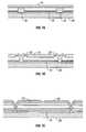
- FIGS. 7A-7Cillustrate three different embodiments of the moving mirror structure.
- FIG. 7Ais a cross section of the embodiment of FIG. 1 , where a strip of metal material 14 is deposited on orthogonally extending supports 18 .
- FIG. 7Bthe moveable reflective material 14 is attached to supports at the corners only, on tethers 32 .
- FIG. 7Cthe moveable reflective material 14 is suspended from a deformable layer or mechanical layer 34 .
- This embodimenthas benefits because the structural design and materials used for the reflective material 14 can be optimized with respect to the optical properties, and the structural design and materials used for the deformable layer 34 can be optimized with respect to desired mechanical properties.
- the production of various types of interferometric devicesis described in a variety of published documents, including, for example, U.S. Published Application 2004/0051929.
- a wide variety of known techniquesmay be used to produce the above described structures involving a series of material deposition, patterning, and etching steps.
- FIG. 8Aillustrates an embodiment of a MEMS device 100 in a side cross-sectional view.
- the MEMS device 100is constructed on a substrate 101 made in one embodiment of glass although not limited thereto.
- An optical layer 103is formed on the substrate 101 .
- the optical layer 103acts as a partial mirror as it both reflects and transmits some of the incident light.
- the optical layer 103may be conductive and may be patterned into rows (not illustrated).
- a dielectric layer 105may be formed over the optical layer 103 .
- a mechanical layer 107is located such that one of its surfaces faces the dielectric layer 105 in a substantially parallel plane and spaced relationship.
- the dielectric layer 105prevents electrical shortage of the optical layer 103 and mechanical layer 107 in a driven state, which will be described below, and further protects the two layers 103 and 107 from damage by impact when the mechanical layer is driven to contact the optical layer 103 .
- the surface 108 of the mechanical layer 107 opposing the dielectric layer 105is highly reflective and acts as a mirror.
- the reflective surface 108 of the mechanical layeris referred to as the “mirror surface”.
- the mechanical layer 107may be conductive and patterned into columns (not illustrated).
- a physical cavity 109is created between the dielectric layer 105 and the mechanical layer 107 .
- the cavity 109is often referred to as an “interferometric cavity” although a depth 113 of the interferometric cavity is defined between the mechanical layer 107 and the optical layer 103 rather than the dielectric layer 105 .
- One of ordinary skill in the artwill appreciate processes for manufacturing of the MEMS device 100 and an array thereof, which is a two-dimensional arrangement of a plurality of the MEMS devices 100 (not illustrated).
- the MEMS device 100is operated by applying or not applying an electric potential between the optical layer 103 and the mechanical layer 107 .
- FIG. 8Athe MEMS device 100 is illustrated in the configuration produced when no voltage is applied between the optical layer 103 and mechanical layer 107 , which is referred to as an “undriven state” or “undriven configuration”.
- an “undriven state” or “undriven configuration”In this state, light that is incident on the MEMS device 100 through the substrate 101 is interferometrically modulated, which will be well appreciated by one of ordinary skill in the art.
- a certain wavelength of the lightis reflected to the viewer. If the selected wavelength of the light is visible, a colored light corresponding to the wavelength is displayed.
- the mechanical layer 107is driven to deform and contact the dielectric layer 105 , as illustrated in FIG. 8B .
- This configuration of the MEMS device 100is referred to as a “driven state” or “driven configuration”.
- the MEMS device 100is in an induced absorption mode, in which most of the light incident on the substrate 101 is absorbed with the result that the surface 111 of the substrate 100 appears black to the viewer.
- the other MEMS devices disclosed herein and their variantswill operate in the same or similar ways, unless specifically discussed otherwise.
- the “driven state”could also result in an interferometric color reflection depending on the thickness of the dielectric layer 105 .
- FIGS. 8C and 8Dillustrate another embodiment of a MEMS device 200 .
- the MEMS device 200is constructed on a substrate 201 and comprises an optical layer 203 , dielectric layer 205 and a mechanical layer 207 .
- the substrate 201 , optical layer 203 and dielectric layer 205have generally the same characteristics and features as the respective layers 101 , 103 and 105 of the MEMS device 100 , unless specifically stated otherwise.
- a mirror 211is provided between the mechanical layer 207 and the dielectric layer 203 .
- the mirror 211has a highly reflective surface 208 and is electrically conductive.
- the mirror 211 of the MEMS device 200is mechanically and electrically connected to the mechanical layer 207 via a connection 215 .
- the mechanical layer 207does not have to have a reflective surface.
- the mechanical layer 207is dedicated to the function of mechanical movement by deformation, and the mirror 211 is dedicated to the function of a mirror as an optical element.
- An interferometric cavity 209is formed between the mirror surface 208 and the dielectric layer 205 .
- the depth of the cavity 213is the distance between the mirror surface 208 and the optical layer 203 (not the dielectric layer 205 ).
- the MEMS device 200is illustrated in the configuration of its undriven state, where no voltage is applied between the optical layer 203 and the mechanical layer 207 (or the mirror 211 ).
- the MEMS device 200is in its driven state, where a voltage greater than a threshold voltage is applied between the optical layer 203 and the mechanical layer 207 (or the mirror 211 ).
- the mechanical layer 207deforms and the reflective surface 408 of the mirror (hereinafter “mirror surface” 208 ) contacts the dielectric layer 205 .
- FIG. 9illustrates the relationship between the movement of the mirror surface 108 / 208 of an interferometric modulator and the electric potential difference between the optical layer 103 / 203 and the mirror surface 108 / 208 of the interfeometric modulator.
- the horizontal axisrepresents the voltage (V O-Mi ), which is the difference between the voltage (V O ) of the optical layer 103 / 203 and the voltage (V Mi ) of the mirror surface 108 / 208 .
- the voltage applied to the mirror surface 108 / 208is the same (equipotential) as that of the mechanical layer 107 / 207 as they are electrically connected.
- the vertical axisrepresents the movement or displacement (x) of the mirror surface 108 / 208 from its position in its undriven state in the direction toward the optical layer 103 / 203 and substantially perpendicular to the mirror surface 108 / 208 in its undriven state.
- a voltageis applied between the optical layer 103 / 203 and mechanical layer 107 / 207 , the mechanical layer 107 / 207 is driven to deform, and accordingly the mirror surface 108 / 208 moves toward the optical layer 103 / 203 .
- the displacement 304 of the mirror surface 108 / 208is substantially proportional to the increase or decrease of the voltage difference (V O-Mi ) until it reaches a threshold voltage (V th ).
- the maximum displacement (D)is shorter than the maximum depth of the interferometric cavity 113 by the thickness of the dielectric layer 105 / 205 .
- the displacement of the mirror surface (D th ) at the threshold voltageis about one third (1 ⁇ 3) of the maximum displacement (D).
- the mirror surface 108 / 208responds to the changes of the voltage difference (V O-Mi ) from its undriven position up until about one third of the maximum displacement (D).
- V O-Mithe voltage difference
- the interferometric cavity depth 113 / 213 of the MEMS device 100 / 200is highly tunable by changing the voltage (V O-Mi ) applied between the optical layers 103 / 203 and the mechanical layer 107 / 207 .
- the mirror surface 108 / 208rapidly moves in reply to a very small change in the voltage difference (V O-Mi ) when the voltage difference (V O-Mi ) becomes greater than the threshold voltage (V th ).
- V ththe threshold voltage
- the major forces acting on the mirror surface 108are 1) an electrostatic force between the optical layer 103 and the mechanical layer 107 , and 2) a mechanical restoration force of the mechanical layer 107 .
- the electrostatic force between the optical layer 103 and the mechanical layer 107is dependent on the potential difference between the two layers 103 and 107 .
- the electrostatic forcemay be created as either attractive or repulsive, it is desirable to have the force maintained as attractive in the operation of the MEMS device 100 .
- the mechanical layer 107(being less rigid than the optical layer 103 in this embodiment) moves towards the optical layer 103 .
- either or both of the layers 103 and 107may move toward the other.
- the electrostatic forceis represented by the following equations:
- F eO-Mirepresents electrostatic force exerted on the mirror surface 108 caused by the voltage applied between the optical layer 103 and the mirror surface 108 .
- C O-Mirepresents capacitance between two electrodes, which are the optical layer 103 and the mirror surface 108 .
- ⁇is the effective permittivity of the materials placed between two electrodes, which are again the optical layer 103 and the mirror surface 108 .
- Ais an effective overlapping area of the two opposing electrodes, which is in this case the area of the mirror surface 108 .
- the parameter “d”is a distance between two opposing electrodes, which is in this case the distance 413 between the mirror surface 108 and the optical layer 103 in the undriven configuration as illustrated in FIG. 1 .
- “x”represents a displacement of the mirror surface 108 toward the optical layer 103 from its position in the undriven configuration.
- the mechanical restoration forceexists in the mechanical layer 107 when it has changed its configuration from its most stable configuration.
- the mechanical restoration forcedepends on the properties of the material used in the mechanical layer 107 and the geometrical configuration of the mechanical layer 107 .
- One of ordinary skill in the artwill appreciate the relationship between the geometrical configuration of the mechanical layer 107 and the restoration force upon selection of an appropriate material for the mechanical layer 107 . Also, one of ordinary skill in the art will be able to design the geometrical configuration of the mechanical layer 107 to create a desired size of the restoration force of the mechanical layer upon the selection of an appropriate material.
- the attractive electrostatic force created by the voltage (V O-Mi ) applied between the layers 103 and 107substantially equilibrates with the mechanical restoration force of the mechanical layer 107 at any point of the first segment 301 .
- the attractive electrostatic force between the optical layer 103 and the mechanical layer 107is significantly larger than the mechanical restoration force in the opposite direction.
- Embodiments of the inventionenable tuning of the interferometric cavity depth of a MEMS device in both of the first and second segments 301 and 303 (0 ⁇ x ⁇ D).
- embodiments of the inventionmay use one or more forces other than the forces identified above, which are the mechanical restoration force of a mechanical layer and the electrostatic force between a mirror surface and an optical layer.
- Embodiments of the inventionmake displacement of the mirror surface have a tunable relationship, preferably a substantially linear relationship, with changes in voltages applied between one or more sets of electrodes.
- a MEMS device 400is formed on a substrate 401 .
- the MEMS device 400comprises an optical layer 403 , a dielectric layer 405 and a mechanical layer 407 .
- the substrate 401 , optical layer 403 and dielectric layer 405have generally the same characteristics and features as the corresponding layers of the MEMS device 100 , unless specifically stated otherwise.
- the mechanical layer 407comprises an area of insulation material, which is referred to as an insulator 415 .
- a mirror 411is located between the dielectric layer 405 and the mechanical layer 407 .
- the mirrorhas a highly reflective surface 408 and is made of a conductive material.
- the mirror 411is mechanically connected to the mechanical layer 407 via the insulator 415 .
- the mirror 411is electrically disconnected or isolated from the mechanical layer 407 while mechanically connected thereto by the insulator 415 .
- the mirror 411may be electrically connected to another electric voltage or current source, which is independent of the mechanical layer 407 .
- the mechanical layer 407is conductive and patterned into columns (not illustrated).
- a cavity 409is formed between the mirror surface 408 and the dielectric layer 405 .
- the depth of the interferometric cavity 413is the distance between the mirror surface 408 and the optical layer 403 (not the dielectric layer 405 ).
- One of ordinary skill in the artwill appreciate processes available for the manufacturing of the MEMS device 400 and an array thereof comprising a plurality of the MEMS devices 404 arranged in a two-dimensional plane. Particularly, one of ordinary skill in the art will appreciate processes and materials available for forming the insulator 415 in the middle of the mechanical layer 407 and for forming the mirror 411 so as to be mechanically connected to but electrically isolated from the mechanical layer.
- movement of the mirror surface 408 within the first segment 301 (0 ⁇ x ⁇ D/3 in FIG. 9 ) and within the second segment 303 (D/3 ⁇ x ⁇ D in FIG. 9 )is tuned or controlled by electric potential differences between different two or more sets of electrodes. More specifically, movement of the mirror surface 408 within the first segment 301 (0 ⁇ x ⁇ D/3) is tuned by the difference between a voltage (V Mi ) of the mirror 411 and a voltage (V O ) of the optical layer 403 while maintaining a voltage (V Mi ) of the mirror 411 and a voltage (V Me ) of the mechanical layer 407 at the same level.
- the movement of the mirror surface 408 within the second segment 303may be tuned by the difference between a voltage (V Mi ) of the mirror 411 and a voltage (V Me ) of the mechanical layer 407 while maintaining or changing a voltage difference between the mirror 411 and the optical layer 403 .
- the displacement of the mirror 411 or mirror surface 408 in response to the electric potential difference between the optical layer 403 and the mirror 411follows the relationship discussed above with reference to FIG. 9 if the voltage at the mirror 411 is maintained the same as the mechanical layer 407 .
- the displacement of the mirror 411 within the first segment 301is generally proportional to the voltage (V O-Mi ), which is the difference between the voltage (V O ) of the optical layer 403 and the voltage (V Mi ) of the mirror 411 .
- the displacement of the mirroris represented by the solid line 304 of FIG. 9 .
- the proportional or tunable relationshipis accomplished by equilibrium of the mechanical restoration force in the mechanical layer 407 with the attractive electrostatic force between the mirror 411 and the optical layer 403 .
- the displacement of the mirror in the second segment 303 by an infinitesimal increase of the voltage (V O-Mi ) beyond the threshold voltage (V th )is represented by the solid line 305 of FIG. 9 .
- the electrostatic attractive force between the optical layer 403 and the mirror 411 created by the potential difference (V O-Mi )may be balanced by the mechanical restoration force of the mechanical layer 407 and by an electrostatic force created by the voltage (V Mi-Me ), which is the difference between the voltage (V Mi ) of the mirror 411 and the voltage (V Me ) of the mechanical layer 407 .
- V Mi-Methe voltage created by the voltage (V Mi-Me ) of the mechanical layer 407 .
- equilibrium of the forces exerted to the mirror 411can be maintained throughout the second segment 303 or at least a portion of the second segment.
- the displacement of the mirror 411may be tunable by changing the voltage (V Mi-Me ).
- the dashed line 307 of FIG. 9represents an example of the tunable displacement of the mirror 411 in the second segment.
- F eMi-Merepresents the electrostatic force exerted on the mirror 411 created by the voltage (V Mi-Me ) applied between the mechanical layer 407 and the mirror 411 .
- C Mi-Merepresents capacitance between two electrodes, which are the mirror 411 and the mechanical layer 407 .
- ⁇is the effective permittivity of the materials located between two electrodes, which are again the mirror 411 and the mechanical layer 407 .
- Ais an effective overlapping area of the two opposing electrodes, which is in this case the area of a surface 417 of the mirror facing the mechanical layer 407 .
- “d′”is a distance between the two electrodes, which is in this case the distance 419 between the mechanical layer 407 and the surface 417 of the mirror in the undriven configuration as illustrated in FIG. 10A .
- “x”represents the displacement of the mirror 411 or mirror surface 408 in the direction toward the optical layer 403 from its position in the undriven configuration.
- the location of the mirror surface 408may be tuned by creating equilibrium among all the forces exerted on the mirror 411 .
- the net force applied to the mirror 411is substantially zero at any position of the mirror 411 .
- the electrostatic forcesfor example, there are electrostatic forces based on the voltage (V O-Mi ) between the mirror 411 and the optical layer 403 , the voltage (V Mi-Me ) between the mirror 411 and the mechanical layer 407 , and the voltage (V Me-O ) between the mechanical layer 407 and the optical layer 403 .
- the relationship among the forcesmay be represented by the following equation.
- F eO-Mi +F eO-MeF mR +F eMi-Me Equation 5
- F mRrepresents the mechanical restoration force of the mechanical layer 407 , which is determined by the configuration and material of the mechanical layer 407 .
- F eO-Mirepresents the electrostatic force created by the voltage difference (V O-Mi ) between the optical layer 403 and the mirror 411 . See Equation 1 above.
- F eMi-Merepresents the electrostatic force created by the voltage (V Mi-Me ) applied between the mirror 411 and the mechanical layer 407 .
- F eO-Merepresents the electrostatic force created by the voltage (V O-Me ) applied between the optical layer 403 and the mechanical layer 407 .
- the force “F eO-Me ”will be smaller than the other forces in Equation 5 as the mirror 411 shields the mechanical layer 407 from the optical layer 403 .
- One of ordinary skill in the artwill be able to formulate an equation representing “F eO-Me ” in view of the slanting or deforming configuration of the mechanical layer 407 when the MEMS device 400 is in a driven state as illustrated in FIG. 10B .
- One of ordinary skill in the artwill be able to formulate an equation more accurately representing the equilibrium of various forces applied to the mirror in a particular MEMS architecture by considering additional forces in the MEMS device 400 .
- the extension 418 of the mirror 411is structurally connected with a part of the MEMS device 400 or the array thereof (not illustrated), mechanical forces caused by such structural connection will be considered in creating the conditions for the equilibrium among the forces acting on the mirror 411 .
- FIG. 11illustrates exemplary voltage differences applied among the three electrodes (mirror 411 , mechanical layer 407 and optical layer 403 ) to create a highly tunable MEMS device.
- first segment 301the voltages of the optical layer 403 and the mirror 411 are maintained at the same level, and the voltage difference (V Mi-Me ) between the mirror 411 and the mechanical layer 407 can be changed between zero and the threshold voltage (V th ).
- the mirror 411may move or stay within the first segment 301 (0 ⁇ x ⁇ D/3), for example, along the line 304 of FIG. 9 .
- the voltage difference (V Mi-Me ) between the mirror 411 and the mechanical layer 407may further change to create equilibrium among the forces applied to the mirror 411 . Accordingly, the mirror 411 may move or stay within the second segment 303 (D/3 ⁇ x ⁇ D), for example, along the line 307 of FIG. 9 .
- Actual voltage differences (V Mi-Me ) and (V O-Mi ) to create the balance among the forcesmay differ from those illustrated in FIG. 11 , depending upon other factors, including the strength of the mechanical restoring forces of the mechanical layer 407 and/or the extension 418 .
- the location of the mirror 411may be tuned by creating equilibrium among the forces applied to the mirror while maintaining the voltage difference (V O-Mi ) between the optical layer 403 and the mirror 411 substantially constant when the mirror is moving within at least a portion of the second segment (D/3 ⁇ x ⁇ D).
- the location of the mirrorcan be tuned while maintaining the voltage difference (V Mi-Me ) between the mirror 411 and the mechanical layer substantially constant when the mirror is moving within at least a portion of the second segment (D/3 ⁇ x ⁇ D).
- the equilibrium of the forces applied to the mirror 411can be accomplished by controlling the voltage differenes (V Mi-Me ) and (V O-Mi ) in a number of different ways.
- the tunable MEMS deviceprovides an analog device that is tunable substantially throughout a range of linear or non-linear movement of the mirror 411 within an interferometric cavity.
- the analog MEMS devicemay be used as a reflective display element tunable to any colored visible light or tunable to any wavelength of light, including radio frequency.
- the analog MEMS devicemay be used as a completely tunable capacitor.
- various parameters of the MEMS devicesmay be changed, which affect the size of the above-described forces to create a desired relationship between the movement of the mirror 411 and the potential difference(s) applied to electrodes of a MEMS device.
- the parameters affecting the size of the restoration forceinclude the properties of the material used for the mechanical layer 407 and its geometrical configuration.
- the parameters affecting the size of the electrostatic forcesare an effective overlapping area of two opposing electrodes (A), dielectric permittivity ( ⁇ ), and a distance between two electrodes (d or d′) in Equations (1-4).
- an analog MEMS devicemay be used as a tunable capacitor as it can store charges on the electrodes embedded in the MEMS device.
- the capacitance between two electrodesmay be tunable because it is inversely proportional to the displacement of the mirror (Equations 2 and 4) and the displacement of the mirror is tunable by voltages changes applied to the electrodes of the MEMS device as discussed above.
- the capacitance of the tunable capacitorcan be further adjustable by changing various parameters of the MEMS device, including the effective overlapping area of two opposing electrodes (A), dielectric permittivity ( ⁇ ), and distance between two electrodes (d or d′).
- FIGS. 12A and 12Billustrate an embodiment of an MEMS device 600 , wherein an optical layer 603 is formed only in a partial area of the optical layer 403 of the MEMS device 400 illustrated in FIG. 10A .
- FIG. 12Bis a plan cross-sectional view of the MEMS device 600 taken along the line A-A indicated in FIG. 12A and being parallel with the surface of the substrate 401 .
- the optical layer 603is formed in a configuration in which the optical layer 603 surrounds a square or rectangular dielectric layer 605 .
- This embodimentprovides a reduced the area of the optical layer 603 , and therefore the effective overlapping area of the optical layer 603 with the mirror surface 408 and the mechanical layer 407 .
- the capacitance of the tunable MEMS capacitorcan be adjusted.
- the size of the optical layer 603affects the effective overlapping area in Equation 2 above and will affect the electrostatic forces, F eO-Mi (Equation 1). On the other hand, the size of the optical layer 603 does not affect the other electrostatic force, F eMi-Me (Equation 3).
- the parameter Amay be designed by altering the size, location and/or geometry of the mechanical layer 107 and/or one or both of the mirror surfaces 408 and 417 .
- FIG. 13illustrates an embodiment of an MEMS device 700 , in which a layer 701 of a non-conductive material is formed on the mirror 411 facing the mechanical layer 407 .
- the layer 701is provided to adjust the dielectric permittivity in Equation 4 above, and therefore affect the electrostatic force F eMi-Me while not affecting the other electrostatic force, F eO-Mi or F eO-Me .
- the dielectric permittivitywill depend on the material of the layer 701 .
- One of ordinary skill in the artwill be able to select an appropriate non-conductive or dielectric material to provide a desired dielectric permittivity in a particular design of the MEMS device 700 .
- a dielectric layermay be formed on a surface of the mechanical layer 407 facing the mirror 411 .
- a dielectric layermay be formed on the mirror surface 408 .
- another dielectric layermay be formed on the dielectric layer 405 , in which the other dielectric layer is formed of a material different from that of the dielectric layer 405 .
- dielectric layersin the size, thickness and/or location.
- FIG. 14illustrates an embodiment of a MEMS device 800 , in which a mirror 811 has a thickness greater than that of the MEMS device 400 while all the other conditions are the same.
- the design of a thicker mirror 811changes the distances between the electrodes in the MEMS device 400 . If the distance (d) between the optical layer 403 and the mirror surface 408 remains the same as in the MEMS device 400 , the distance (d′) between the mechanical layer 407 and the surface 417 of the mirror 411 will be shorter if the mirror 811 is designed to be thicker.
- the distance (d′)affects the force, F eMi-Me , (Equations 3 and 4) while not affecting the other force, F eO-Mi (Equations 1 and 2).
- the thickness of the mirrorone or both of the distances (d) and (d′) may be altered. By varying the distances (d) and (d′), the capacitance of the tunable MEMS capacitor can be adjusted.
- the mirror 411is neither mechanically nor electrically connected to the mechanical layer 407 .
- the insulator 415 of the MEMS device 900 which mechanically connects the mirror 411 and the mechanical layer 407is lacking. Due to this lack of mechanical connection, there may be no mechanical restoration force exerted on the mirror 411 . Thus, the movement of the mirror 411 may be equilibrated only by the electrostatic forces including F eMi-Me and F eO-Mi .
- the extension 418 of the mirror 411may have a structural or mechanical connection with a part of the MEMS device 900 or an array thereof (not illustrated).
- a restoration force from such a structural connectionmay be exerted on the mirror 411 in addition to the above-electrostatic forces, all of which will be equilibrate to achieve the tenability between the movement of the mirror 411 and voltages applied to the electrodes of the MEMS device 900 , including the optical layer 403 , the mechanical layer 407 and the mirror 411 .
- MEMS devicesmay be operated as an analog device over full range of the movement of the mirror.
- These tunable analog MEMS devicesmay be used to select any wavelengths of light by its interferometric modulation from the light incident to the MEMS device.
- the MEMS devicesmay select radio frequencies and may operate as an RF MEMS device.
- the tunable MEMS devices of the foregoing embodimentscan be fabricated utilizing conventional thin layer forming processes. For example, a partially transparent and electrically conductive layer is deposited on a transparent substrate to provide the optical layer 403 .
- the dielectric layer 405is deposited over the optical layer 403 .
- a first sacrificial layer(not shown) is formed over the dielectric layer 405 .
- a reflective materialis deposited over the first sacrificial layer, and a portion of the reflective material is selectively etched to form the mirror 411 .
- a second sacrificial layer(not shown) is formed over the layer for the mirror 411 and over the first sacrificial layer surrounding the mirror 411 .
- the first and second sacrificial layersare selectively etched to form a plurality of holes exposing the dielectric layer 405 .
- the holesare filled with a dielectric material to form posts (not shown).
- a conductive material which will later form the mechanical layer 407is deposited over the posts and the second sacrificial layer.
- the postssupport the mechanical layer 407 separated from the dielectric layer 405 with a gap therebetween once the first and second sacrificial layers are removed.
- the mechanical layer 407is selectively etched to form an opening, which exposes the second sacrificial layer.
- An insulating materialis deposited in the opening of the mechanical layer 407 to form an insulating portion, which will become the insulator 415 later.
- a third sacrificial layer(not shown) is formed over the mechanical layer 407 .
- the third sacrificial layeris selectively etched to form a plurality of holes, which expose the mechanical layer 407 , and a dielectric material is filled in the holes.
- a conductive layer, which will become the conductive extension 418 to the mirror 411is formed over the third sacrificial layer including the dielectric material filling the holes.
- the dielectric materialsform posts (not shown) supporting the conductive extension 418 to suspend over the mechanical layer 407 .
- An openingis formed through the third sacrificial layer, the insulating portion of the mechanical layer 407 and the second sacrificial layer to expose the mirror 411 .
- the openingis filled with a conductive material, which electrically connects the mirror and the conductive extension 418 .
- openingsare formed to expose the first, second and third sacrificial layers, and an etchant is supplied to the exposed portion of the sacrificial layers through the openings.
- the etchantreacts with the materials of the sacrificial layers, which turns the sacrificial materials to gas. As a result, the spaces filled with the sacrificial materials become cavities and the MEMS device of FIG. 10A is formed.
- One of ordinary skill in the artwill be able to determine various conditions of the process steps and materials to be used in the processes. Also, one of ordinary skill in the art will appreciate that there are many alternative processes to fabricate tunable MEMS devices.
Landscapes
- Physics & Mathematics (AREA)
- General Physics & Mathematics (AREA)
- Optics & Photonics (AREA)
- Spectroscopy & Molecular Physics (AREA)
- Mechanical Light Control Or Optical Switches (AREA)
- Magnetic Resonance Imaging Apparatus (AREA)
- Surface Acoustic Wave Elements And Circuit Networks Thereof (AREA)
- Soundproofing, Sound Blocking, And Sound Damping (AREA)
Abstract
Description
FeO-Mi+FeO-Me=FmR+FeMi-Me Equation 5
Claims (21)
Priority Applications (13)
| Application Number | Priority Date | Filing Date | Title |
|---|---|---|---|
| US11/144,546US8008736B2 (en) | 2004-09-27 | 2005-06-03 | Analog interferometric modulator device |
| DE602005018665TDE602005018665D1 (en) | 2004-09-27 | 2005-08-22 | ANALOG INTERFEROMETRIC MODULATOR DEVICE |
| KR1020077006100AKR20070061821A (en) | 2004-09-27 | 2005-08-22 | Analog interference modulator appliance |
| CA002577335ACA2577335A1 (en) | 2004-09-27 | 2005-08-22 | Analog interferometric modulator device |
| EP05790217AEP1800160B1 (en) | 2004-09-27 | 2005-08-22 | Analog interferometric modulator device |
| PCT/US2005/029899WO2006036392A1 (en) | 2004-09-27 | 2005-08-22 | Analog interferometric modulator device |
| AT05790217TATE453873T1 (en) | 2004-09-27 | 2005-08-22 | ANALOG INTERFEROMETRIC MODULATOR DEVICE |
| TW094130741ATW200626942A (en) | 2004-09-27 | 2005-09-07 | Analog interferometric modulator device |
| PCT/US2005/032782WO2006036560A2 (en) | 2004-09-27 | 2005-09-14 | Mems switches with deforming membranes |
| EP05798437AEP1809568A2 (en) | 2004-09-27 | 2005-09-14 | Mems switches with deforming membranes |
| MX2007003577AMX2007003577A (en) | 2004-09-27 | 2005-09-14 | Mems switches with deforming membranes. |
| JP2007533542AJP2008515150A (en) | 2004-09-27 | 2005-09-14 | MEMS switch with deformable thin film |
| TW094133425ATW200635845A (en) | 2004-09-27 | 2005-09-26 | MEMS switches with deforming membranes |
Applications Claiming Priority (2)
| Application Number | Priority Date | Filing Date | Title |
|---|---|---|---|
| US61346504P | 2004-09-27 | 2004-09-27 | |
| US11/144,546US8008736B2 (en) | 2004-09-27 | 2005-06-03 | Analog interferometric modulator device |
Publications (2)
| Publication Number | Publication Date |
|---|---|
| US20060065940A1 US20060065940A1 (en) | 2006-03-30 |
| US8008736B2true US8008736B2 (en) | 2011-08-30 |
Family
ID=35428159
Family Applications (1)
| Application Number | Title | Priority Date | Filing Date |
|---|---|---|---|
| US11/144,546Expired - Fee RelatedUS8008736B2 (en) | 2004-09-27 | 2005-06-03 | Analog interferometric modulator device |
Country Status (8)
| Country | Link |
|---|---|
| US (1) | US8008736B2 (en) |
| EP (1) | EP1800160B1 (en) |
| KR (1) | KR20070061821A (en) |
| AT (1) | ATE453873T1 (en) |
| CA (1) | CA2577335A1 (en) |
| DE (1) | DE602005018665D1 (en) |
| TW (1) | TW200626942A (en) |
| WO (1) | WO2006036392A1 (en) |
Cited By (14)
| Publication number | Priority date | Publication date | Assignee | Title |
|---|---|---|---|---|
| US20110235156A1 (en)* | 2010-03-26 | 2011-09-29 | Qualcomm Mems Technologies, Inc. | Methods and devices for pressure detection |
| US8638491B2 (en) | 2004-09-27 | 2014-01-28 | Qualcomm Mems Technologies, Inc. | Device having a conductive light absorbing mask and method for fabricating same |
| US20140092110A1 (en)* | 2012-10-01 | 2014-04-03 | Qualcomm Mems Technologies, Inc. | Electromechanical systems device with protrusions to provide additional stable states |
| US8693084B2 (en) | 2008-03-07 | 2014-04-08 | Qualcomm Mems Technologies, Inc. | Interferometric modulator in transmission mode |
| US8736939B2 (en) | 2011-11-04 | 2014-05-27 | Qualcomm Mems Technologies, Inc. | Matching layer thin-films for an electromechanical systems reflective display device |
| US8797632B2 (en) | 2010-08-17 | 2014-08-05 | Qualcomm Mems Technologies, Inc. | Actuation and calibration of charge neutral electrode of a display device |
| US20140218786A1 (en)* | 2011-05-04 | 2014-08-07 | Qualcomm Mems Technologies, Inc. | Devices and methods for achieving non-contacting white state in interferometric modulators |
| US8928967B2 (en) | 1998-04-08 | 2015-01-06 | Qualcomm Mems Technologies, Inc. | Method and device for modulating light |
| WO2015026333A1 (en)* | 2013-08-20 | 2015-02-26 | Intel Corporation | A display apparatus including mems devices |
| US8971675B2 (en) | 2006-01-13 | 2015-03-03 | Qualcomm Mems Technologies, Inc. | Interconnect structure for MEMS device |
| US9086564B2 (en) | 2004-09-27 | 2015-07-21 | Qualcomm Mems Technologies, Inc. | Conductive bus structure for interferometric modulator array |
| US9110289B2 (en) | 1998-04-08 | 2015-08-18 | Qualcomm Mems Technologies, Inc. | Device for modulating light with multiple electrodes |
| US9554213B2 (en) | 2012-10-01 | 2017-01-24 | The Research Foundation For The State University Of New York | Hinged MEMS diaphragm |
| US20210263298A1 (en)* | 2012-09-12 | 2021-08-26 | Seiko Epson Corporation | Optical Module, Electronic Device, And Driving Method |
Families Citing this family (83)
| Publication number | Priority date | Publication date | Assignee | Title |
|---|---|---|---|---|
| US7123216B1 (en) | 1994-05-05 | 2006-10-17 | Idc, Llc | Photonic MEMS and structures |
| US7532377B2 (en) | 1998-04-08 | 2009-05-12 | Idc, Llc | Movable micro-electromechanical device |
| WO2003007049A1 (en) | 1999-10-05 | 2003-01-23 | Iridigm Display Corporation | Photonic mems and structures |
| TWI289708B (en) | 2002-12-25 | 2007-11-11 | Qualcomm Mems Technologies Inc | Optical interference type color display |
| US7342705B2 (en) | 2004-02-03 | 2008-03-11 | Idc, Llc | Spatial light modulator with integrated optical compensation structure |
| EP2246726B1 (en) | 2004-07-29 | 2013-04-03 | QUALCOMM MEMS Technologies, Inc. | System and method for micro-electromechanical operating of an interferometric modulator |
| US7583429B2 (en) | 2004-09-27 | 2009-09-01 | Idc, Llc | Ornamental display device |
| US7944599B2 (en)* | 2004-09-27 | 2011-05-17 | Qualcomm Mems Technologies, Inc. | Electromechanical device with optical function separated from mechanical and electrical function |
| US7936497B2 (en) | 2004-09-27 | 2011-05-03 | Qualcomm Mems Technologies, Inc. | MEMS device having deformable membrane characterized by mechanical persistence |
| US7372613B2 (en)* | 2004-09-27 | 2008-05-13 | Idc, Llc | Method and device for multistate interferometric light modulation |
| US7630119B2 (en) | 2004-09-27 | 2009-12-08 | Qualcomm Mems Technologies, Inc. | Apparatus and method for reducing slippage between structures in an interferometric modulator |
| US7564612B2 (en) | 2004-09-27 | 2009-07-21 | Idc, Llc | Photonic MEMS and structures |
| US7612932B2 (en)* | 2004-09-27 | 2009-11-03 | Idc, Llc | Microelectromechanical device with optical function separated from mechanical and electrical function |
| US7554714B2 (en) | 2004-09-27 | 2009-06-30 | Idc, Llc | Device and method for manipulation of thermal response in a modulator |
| US7304784B2 (en) | 2004-09-27 | 2007-12-04 | Idc, Llc | Reflective display device having viewable display on both sides |
| US7327510B2 (en)* | 2004-09-27 | 2008-02-05 | Idc, Llc | Process for modifying offset voltage characteristics of an interferometric modulator |
| US7884989B2 (en)* | 2005-05-27 | 2011-02-08 | Qualcomm Mems Technologies, Inc. | White interferometric modulators and methods for forming the same |
| US7460292B2 (en)* | 2005-06-03 | 2008-12-02 | Qualcomm Mems Technologies, Inc. | Interferometric modulator with internal polarization and drive method |
| US7550810B2 (en) | 2006-02-23 | 2009-06-23 | Qualcomm Mems Technologies, Inc. | MEMS device having a layer movable at asymmetric rates |
| US8004743B2 (en)* | 2006-04-21 | 2011-08-23 | Qualcomm Mems Technologies, Inc. | Method and apparatus for providing brightness control in an interferometric modulator (IMOD) display |
| US20070268201A1 (en)* | 2006-05-22 | 2007-11-22 | Sampsell Jeffrey B | Back-to-back displays |
| US7649671B2 (en)* | 2006-06-01 | 2010-01-19 | Qualcomm Mems Technologies, Inc. | Analog interferometric modulator device with electrostatic actuation and release |
| US7471442B2 (en) | 2006-06-15 | 2008-12-30 | Qualcomm Mems Technologies, Inc. | Method and apparatus for low range bit depth enhancements for MEMS display architectures |
| US7385744B2 (en) | 2006-06-28 | 2008-06-10 | Qualcomm Mems Technologies, Inc. | Support structure for free-standing MEMS device and methods for forming the same |
| US7835061B2 (en) | 2006-06-28 | 2010-11-16 | Qualcomm Mems Technologies, Inc. | Support structures for free-standing electromechanical devices |
| US7527998B2 (en) | 2006-06-30 | 2009-05-05 | Qualcomm Mems Technologies, Inc. | Method of manufacturing MEMS devices providing air gap control |
| EP1943551A2 (en) | 2006-10-06 | 2008-07-16 | Qualcomm Mems Technologies, Inc. | Light guide |
| EP1943555B1 (en) | 2006-10-06 | 2012-05-02 | QUALCOMM MEMS Technologies, Inc. | Optical loss structure integrated in an illumination apparatus of a display |
| US7629197B2 (en)* | 2006-10-18 | 2009-12-08 | Qualcomm Mems Technologies, Inc. | Spatial light modulator |
| US20080111834A1 (en)* | 2006-11-09 | 2008-05-15 | Mignard Marc M | Two primary color display |
| US7403180B1 (en)* | 2007-01-29 | 2008-07-22 | Qualcomm Mems Technologies, Inc. | Hybrid color synthesis for multistate reflective modulator displays |
| US8115987B2 (en)* | 2007-02-01 | 2012-02-14 | Qualcomm Mems Technologies, Inc. | Modulating the intensity of light from an interferometric reflector |
| US7742220B2 (en)* | 2007-03-28 | 2010-06-22 | Qualcomm Mems Technologies, Inc. | Microelectromechanical device and method utilizing conducting layers separated by stops |
| US7643202B2 (en)* | 2007-05-09 | 2010-01-05 | Qualcomm Mems Technologies, Inc. | Microelectromechanical system having a dielectric movable membrane and a mirror |
| US7715085B2 (en)* | 2007-05-09 | 2010-05-11 | Qualcomm Mems Technologies, Inc. | Electromechanical system having a dielectric movable membrane and a mirror |
| US8111262B2 (en) | 2007-05-18 | 2012-02-07 | Qualcomm Mems Technologies, Inc. | Interferometric modulator displays with reduced color sensitivity |
| US7643199B2 (en) | 2007-06-19 | 2010-01-05 | Qualcomm Mems Technologies, Inc. | High aperture-ratio top-reflective AM-iMod displays |
| US7782517B2 (en)* | 2007-06-21 | 2010-08-24 | Qualcomm Mems Technologies, Inc. | Infrared and dual mode displays |
| US7630121B2 (en) | 2007-07-02 | 2009-12-08 | Qualcomm Mems Technologies, Inc. | Electromechanical device with optical function separated from mechanical and electrical function |
| EP2183623A1 (en) | 2007-07-31 | 2010-05-12 | Qualcomm Mems Technologies, Inc. | Devices for enhancing colour shift of interferometric modulators |
| US8072402B2 (en)* | 2007-08-29 | 2011-12-06 | Qualcomm Mems Technologies, Inc. | Interferometric optical modulator with broadband reflection characteristics |
| US7773286B2 (en)* | 2007-09-14 | 2010-08-10 | Qualcomm Mems Technologies, Inc. | Periodic dimple array |
| US7847999B2 (en)* | 2007-09-14 | 2010-12-07 | Qualcomm Mems Technologies, Inc. | Interferometric modulator display devices |
| US20090078316A1 (en)* | 2007-09-24 | 2009-03-26 | Qualcomm Incorporated | Interferometric photovoltaic cell |
| CN101828145B (en)* | 2007-10-19 | 2012-03-21 | 高通Mems科技公司 | Displays with integrated photovoltaic elements |
| US8058549B2 (en)* | 2007-10-19 | 2011-11-15 | Qualcomm Mems Technologies, Inc. | Photovoltaic devices with integrated color interferometric film stacks |
| EP2203765A1 (en)* | 2007-10-23 | 2010-07-07 | Qualcomm Mems Technologies, Inc. | Adjustably transmissive mems-based devices |
| US20090293955A1 (en)* | 2007-11-07 | 2009-12-03 | Qualcomm Incorporated | Photovoltaics with interferometric masks |
| US8941631B2 (en) | 2007-11-16 | 2015-01-27 | Qualcomm Mems Technologies, Inc. | Simultaneous light collection and illumination on an active display |
| US8068710B2 (en)* | 2007-12-07 | 2011-11-29 | Qualcomm Mems Technologies, Inc. | Decoupled holographic film and diffuser |
| US7715079B2 (en)* | 2007-12-07 | 2010-05-11 | Qualcomm Mems Technologies, Inc. | MEMS devices requiring no mechanical support |
| WO2009085601A2 (en)* | 2007-12-21 | 2009-07-09 | Qualcom Mems Technologies, Inc. | Multijunction photovoltaic cells |
| US7863079B2 (en) | 2008-02-05 | 2011-01-04 | Qualcomm Mems Technologies, Inc. | Methods of reducing CD loss in a microelectromechanical device |
| WO2009099791A1 (en)* | 2008-02-05 | 2009-08-13 | Qualcomm Mems Technologies, Inc. | Methods of reducing cd loss in a microelectromechanical device |
| US8164821B2 (en) | 2008-02-22 | 2012-04-24 | Qualcomm Mems Technologies, Inc. | Microelectromechanical device with thermal expansion balancing layer or stiffening layer |
| US7612933B2 (en)* | 2008-03-27 | 2009-11-03 | Qualcomm Mems Technologies, Inc. | Microelectromechanical device with spacing layer |
| US7898723B2 (en)* | 2008-04-02 | 2011-03-01 | Qualcomm Mems Technologies, Inc. | Microelectromechanical systems display element with photovoltaic structure |
| US7969638B2 (en)* | 2008-04-10 | 2011-06-28 | Qualcomm Mems Technologies, Inc. | Device having thin black mask and method of fabricating the same |
| US7746539B2 (en)* | 2008-06-25 | 2010-06-29 | Qualcomm Mems Technologies, Inc. | Method for packing a display device and the device obtained thereof |
| US7768690B2 (en) | 2008-06-25 | 2010-08-03 | Qualcomm Mems Technologies, Inc. | Backlight displays |
| US8023167B2 (en)* | 2008-06-25 | 2011-09-20 | Qualcomm Mems Technologies, Inc. | Backlight displays |
| US7859740B2 (en)* | 2008-07-11 | 2010-12-28 | Qualcomm Mems Technologies, Inc. | Stiction mitigation with integrated mech micro-cantilevers through vertical stress gradient control |
| US7855826B2 (en) | 2008-08-12 | 2010-12-21 | Qualcomm Mems Technologies, Inc. | Method and apparatus to reduce or eliminate stiction and image retention in interferometric modulator devices |
| US8358266B2 (en)* | 2008-09-02 | 2013-01-22 | Qualcomm Mems Technologies, Inc. | Light turning device with prismatic light turning features |
| US20100096011A1 (en)* | 2008-10-16 | 2010-04-22 | Qualcomm Mems Technologies, Inc. | High efficiency interferometric color filters for photovoltaic modules |
| US20100125878A1 (en)* | 2008-11-19 | 2010-05-20 | Sony Corporation | Embedded wireless antenna for network tv |
| US8270056B2 (en)* | 2009-03-23 | 2012-09-18 | Qualcomm Mems Technologies, Inc. | Display device with openings between sub-pixels and method of making same |
| CN102449512A (en) | 2009-05-29 | 2012-05-09 | 高通Mems科技公司 | Illumination devices and methods of fabrication thereof |
| US8264548B2 (en)* | 2009-06-23 | 2012-09-11 | Sony Corporation | Steering mirror for TV receiving high frequency wireless video |
| US8279356B2 (en)* | 2009-07-07 | 2012-10-02 | Sony Corporation | Active suppression by TV of white space device interference |
| US8270062B2 (en)* | 2009-09-17 | 2012-09-18 | Qualcomm Mems Technologies, Inc. | Display device with at least one movable stop element |
| US8488228B2 (en)* | 2009-09-28 | 2013-07-16 | Qualcomm Mems Technologies, Inc. | Interferometric display with interferometric reflector |
| US20110078749A1 (en)* | 2009-09-29 | 2011-03-31 | Sony Corporation | Embedded wireless antenna for network tv |
| KR20130100232A (en) | 2010-04-09 | 2013-09-10 | 퀄컴 엠이엠에스 테크놀로지스, 인크. | Mechanical layer of an electromechanical device and methods of forming the same |
| US8848294B2 (en) | 2010-05-20 | 2014-09-30 | Qualcomm Mems Technologies, Inc. | Method and structure capable of changing color saturation |
| US9057872B2 (en) | 2010-08-31 | 2015-06-16 | Qualcomm Mems Technologies, Inc. | Dielectric enhanced mirror for IMOD display |
| US20120236042A1 (en)* | 2011-03-15 | 2012-09-20 | Qualcomm Mems Technologies, Inc. | White point tuning for a display |
| US8963159B2 (en) | 2011-04-04 | 2015-02-24 | Qualcomm Mems Technologies, Inc. | Pixel via and methods of forming the same |
| US9134527B2 (en) | 2011-04-04 | 2015-09-15 | Qualcomm Mems Technologies, Inc. | Pixel via and methods of forming the same |
| US8659816B2 (en) | 2011-04-25 | 2014-02-25 | Qualcomm Mems Technologies, Inc. | Mechanical layer and methods of making the same |
| US9183812B2 (en) | 2013-01-29 | 2015-11-10 | Pixtronix, Inc. | Ambient light aware display apparatus |
| US9372338B2 (en)* | 2014-01-17 | 2016-06-21 | Qualcomm Mems Technologies, Inc. | Multi-state interferometric modulator with large stable range of motion |
| TWI753712B (en)* | 2020-12-21 | 2022-01-21 | 財團法人工業技術研究院 | Microelectromechanical infrared sensing device |
Citations (509)
| Publication number | Priority date | Publication date | Assignee | Title |
|---|---|---|---|---|
| US2534846A (en) | 1946-06-20 | 1950-12-19 | Emi Ltd | Color filter |
| US2590906A (en) | 1946-11-22 | 1952-04-01 | Farrand Optical Co Inc | Reflection interference filter |
| US2677714A (en) | 1951-09-21 | 1954-05-04 | Alois Vogt Dr | Optical-electrical conversion device comprising a light-permeable metal electrode |
| US3247392A (en) | 1961-05-17 | 1966-04-19 | Optical Coating Laboratory Inc | Optical coating and assembly used as a band pass interference filter reflecting in the ultraviolet and infrared |
| US3439973A (en) | 1963-06-28 | 1969-04-22 | Siemens Ag | Polarizing reflector for electromagnetic wave radiation in the micron wavelength |
| US3653741A (en) | 1970-02-16 | 1972-04-04 | Alvin M Marks | Electro-optical dipolar material |
| US3656836A (en) | 1968-07-05 | 1972-04-18 | Thomson Csf | Light modulator |
| US3679313A (en) | 1970-10-23 | 1972-07-25 | Bell Telephone Labor Inc | Dispersive element for optical pulse compression |
| US3725868A (en) | 1970-10-19 | 1973-04-03 | Burroughs Corp | Small reconfigurable processor for a variety of data processing applications |
| US3728030A (en) | 1970-06-22 | 1973-04-17 | Cary Instruments | Polarization interferometer |
| US3813265A (en) | 1970-02-16 | 1974-05-28 | A Marks | Electro-optical dipolar material |
| US3886310A (en) | 1973-08-22 | 1975-05-27 | Westinghouse Electric Corp | Electrostatically deflectable light valve with improved diffraction properties |
| US3955190A (en) | 1972-09-11 | 1976-05-04 | Kabushiki Kaisha Suwa Seikosha | Electro-optical digital display |
| US3955880A (en) | 1973-07-20 | 1976-05-11 | Organisation Europeenne De Recherches Spatiales | Infrared radiation modulator |
| US4099854A (en) | 1976-10-12 | 1978-07-11 | The Unites States Of America As Represented By The Secretary Of The Navy | Optical notch filter utilizing electric dipole resonance absorption |
| US4196396A (en) | 1976-10-15 | 1980-04-01 | Bell Telephone Laboratories, Incorporated | Interferometer apparatus using electro-optic material with feedback |
| US4228437A (en) | 1979-06-26 | 1980-10-14 | The United States Of America As Represented By The Secretary Of The Navy | Wideband polarization-transforming electromagnetic mirror |
| US4377324A (en) | 1980-08-04 | 1983-03-22 | Honeywell Inc. | Graded index Fabry-Perot optical filter device |
| US4389096A (en) | 1977-12-27 | 1983-06-21 | Matsushita Electric Industrial Co., Ltd. | Image display apparatus of liquid crystal valve projection type |
| US4392711A (en) | 1980-03-28 | 1983-07-12 | Hoechst Aktiengesellschaft | Process and apparatus for rendering visible charge images |
| US4403248A (en) | 1980-03-04 | 1983-09-06 | U.S. Philips Corporation | Display device with deformable reflective medium |
| US4421381A (en) | 1980-04-04 | 1983-12-20 | Yokogawa Hokushin Electric Corp. | Mechanical vibrating element |
| US4441789A (en) | 1980-03-31 | 1984-04-10 | Jenoptik Jena Gmbh | Resonance absorber |
| US4441791A (en) | 1980-09-02 | 1984-04-10 | Texas Instruments Incorporated | Deformable mirror light modulator |
| US4445050A (en) | 1981-12-15 | 1984-04-24 | Marks Alvin M | Device for conversion of light power to electric power |
| US4482213A (en) | 1982-11-23 | 1984-11-13 | Texas Instruments Incorporated | Perimeter seal reinforcement holes for plastic LCDs |
| US4497974A (en) | 1982-11-22 | 1985-02-05 | Exxon Research & Engineering Co. | Realization of a thin film solar cell with a detached reflector |
| US4498953A (en) | 1983-07-27 | 1985-02-12 | At&T Bell Laboratories | Etching techniques |
| US4500171A (en) | 1982-06-02 | 1985-02-19 | Texas Instruments Incorporated | Process for plastic LCD fill hole sealing |
| US4519676A (en) | 1982-02-01 | 1985-05-28 | U.S. Philips Corporation | Passive display device |
| US4531126A (en) | 1981-05-18 | 1985-07-23 | Societe D'etude Du Radant | Method and device for analyzing a very high frequency radiation beam of electromagnetic waves |
| US4560435A (en) | 1984-10-01 | 1985-12-24 | International Business Machines Corporation | Composite back-etch/lift-off stencil for proximity effect minimization |
| US4566935A (en) | 1984-07-31 | 1986-01-28 | Texas Instruments Incorporated | Spatial light modulator and method |
| US4571603A (en) | 1981-11-03 | 1986-02-18 | Texas Instruments Incorporated | Deformable mirror electrostatic printer |
| US4596992A (en) | 1984-08-31 | 1986-06-24 | Texas Instruments Incorporated | Linear spatial light modulator and printer |
| US4615595A (en) | 1984-10-10 | 1986-10-07 | Texas Instruments Incorporated | Frame addressed spatial light modulator |
| US4655554A (en) | 1985-03-06 | 1987-04-07 | The United States Of America As Represented By The Secretary Of The Air Force | Spatial light modulator having a capacitively coupled photoconductor |
| US4662746A (en) | 1985-10-30 | 1987-05-05 | Texas Instruments Incorporated | Spatial light modulator and method |
| US4663083A (en) | 1978-05-26 | 1987-05-05 | Marks Alvin M | Electro-optical dipole suspension with reflective-absorptive-transmissive characteristics |
| US4666254A (en) | 1984-01-30 | 1987-05-19 | Sharp Kabushiki Kaisha | Liquid crystal display panel with a metal plate in its terminal portion |
| US4681403A (en) | 1981-07-16 | 1987-07-21 | U.S. Philips Corporation | Display device with micromechanical leaf spring switches |
| US4710732A (en) | 1984-07-31 | 1987-12-01 | Texas Instruments Incorporated | Spatial light modulator and method |
| US4748366A (en) | 1986-09-02 | 1988-05-31 | Taylor George W | Novel uses of piezoelectric materials for creating optical effects |
| US4779959A (en) | 1986-09-05 | 1988-10-25 | The Secretary Of State For Defence In Her Britannic Majesty's Government Of The United Kingdom Of Great Britain And Northern Ireland | Liquid crystal electro-optic modulator in a fabry-perot interferometer |
| US4786128A (en) | 1986-12-02 | 1988-11-22 | Quantum Diagnostics, Ltd. | Device for modulating and reflecting electromagnetic radiation employing electro-optic layer having a variable index of refraction |
| US4790635A (en) | 1986-04-25 | 1988-12-13 | The Secretary Of State For Defence In Her Brittanic Majesty's Government Of The United Kingdom Of Great Britain And Northern Ireland | Electro-optical device |
| EP0310176A2 (en) | 1987-09-30 | 1989-04-05 | Philips Electronics Uk Limited | Method of and arrangement for generating a two-dimensional image |
| US4857978A (en) | 1987-08-11 | 1989-08-15 | North American Philips Corporation | Solid state light modulator incorporating metallized gel and method of metallization |
| US4856863A (en) | 1988-06-22 | 1989-08-15 | Texas Instruments Incorporated | Optical fiber interconnection network including spatial light modulator |
| US4859060A (en) | 1985-11-26 | 1989-08-22 | 501 Sharp Kabushiki Kaisha | Variable interferometric device and a process for the production of the same |
| US4900395A (en) | 1989-04-07 | 1990-02-13 | Fsi International, Inc. | HF gas etching of wafers in an acid processor |
| US4900136A (en) | 1987-08-11 | 1990-02-13 | North American Philips Corporation | Method of metallizing silica-containing gel and solid state light modulator incorporating the metallized gel |
| US4925259A (en) | 1988-10-20 | 1990-05-15 | The United States Of America As Represented By The United States Department Of Energy | Multilayer optical dielectric coating |
| US4937496A (en) | 1987-05-16 | 1990-06-26 | W. C. Heraeus Gmbh | Xenon short arc discharge lamp |
| US4954789A (en) | 1989-09-28 | 1990-09-04 | Texas Instruments Incorporated | Spatial light modulator |
| US4956619A (en) | 1988-02-19 | 1990-09-11 | Texas Instruments Incorporated | Spatial light modulator |
| US4965562A (en) | 1987-05-13 | 1990-10-23 | U.S. Philips Corporation | Electroscopic display device |
| US4973131A (en) | 1989-02-03 | 1990-11-27 | Mcdonnell Douglas Corporation | Modulator mirror |
| US4982184A (en) | 1989-01-03 | 1991-01-01 | General Electric Company | Electrocrystallochromic display and element |
| US5018256A (en) | 1990-06-29 | 1991-05-28 | Texas Instruments Incorporated | Architecture and process for integrating DMD with control circuit substrates |
| US5022745A (en) | 1989-09-07 | 1991-06-11 | Massachusetts Institute Of Technology | Electrostatically deformable single crystal dielectrically coated mirror |
| US5028939A (en) | 1988-08-23 | 1991-07-02 | Texas Instruments Incorporated | Spatial light modulator system |
| US5037173A (en) | 1989-11-22 | 1991-08-06 | Texas Instruments Incorporated | Optical interconnection network |
| US5044736A (en) | 1990-11-06 | 1991-09-03 | Motorola, Inc. | Configurable optical filter or display |
| US5061049A (en) | 1984-08-31 | 1991-10-29 | Texas Instruments Incorporated | Spatial light modulator and method |
| US5062689A (en) | 1990-08-21 | 1991-11-05 | Koehler Dale R | Electrostatically actuatable light modulating device |
| US5075796A (en) | 1990-05-31 | 1991-12-24 | Eastman Kodak Company | Optical article for multicolor imaging |
| US5078479A (en) | 1990-04-20 | 1992-01-07 | Centre Suisse D'electronique Et De Microtechnique Sa | Light modulation device with matrix addressing |
| US5079544A (en) | 1989-02-27 | 1992-01-07 | Texas Instruments Incorporated | Standard independent digitized video system |
| US5083857A (en) | 1990-06-29 | 1992-01-28 | Texas Instruments Incorporated | Multi-level deformable mirror device |
| US5091983A (en) | 1987-06-04 | 1992-02-25 | Walter Lukosz | Optical modulation apparatus and measurement method |
| US5096279A (en) | 1984-08-31 | 1992-03-17 | Texas Instruments Incorporated | Spatial light modulator and method |
| US5099353A (en) | 1990-06-29 | 1992-03-24 | Texas Instruments Incorporated | Architecture and process for integrating DMD with control circuit substrates |
| US5124834A (en) | 1989-11-16 | 1992-06-23 | General Electric Company | Transferrable, self-supporting pellicle for elastomer light valve displays and method for making the same |
| US5136669A (en) | 1991-03-15 | 1992-08-04 | Sperry Marine Inc. | Variable ratio fiber optic coupler optical signal processing element |
| US5142414A (en) | 1991-04-22 | 1992-08-25 | Koehler Dale R | Electrically actuatable temporal tristimulus-color device |
| US5142405A (en) | 1990-06-29 | 1992-08-25 | Texas Instruments Incorporated | Bistable dmd addressing circuit and method |
| DE4108966A1 (en) | 1991-03-19 | 1992-09-24 | Iot Entwicklungsgesellschaft F | Electro-optical interferometric light modulator - uses single crystal with three flat face sides, refractive index being variable by application of electrical or magnetic field |
| US5153771A (en) | 1990-07-18 | 1992-10-06 | Northrop Corporation | Coherent light modulation and detector |
| US5162787A (en) | 1989-02-27 | 1992-11-10 | Texas Instruments Incorporated | Apparatus and method for digitized video system utilizing a moving display surface |
| US5168406A (en) | 1991-07-31 | 1992-12-01 | Texas Instruments Incorporated | Color deformable mirror device and method for manufacture |
| US5170283A (en) | 1991-07-24 | 1992-12-08 | Northrop Corporation | Silicon spatial light modulator |
| US5170156A (en) | 1989-02-27 | 1992-12-08 | Texas Instruments Incorporated | Multi-frequency two dimensional display system |
| US5172262A (en) | 1985-10-30 | 1992-12-15 | Texas Instruments Incorporated | Spatial light modulator and method |
| US5179274A (en) | 1991-07-12 | 1993-01-12 | Texas Instruments Incorporated | Method for controlling operation of optical systems and devices |
| US5192946A (en) | 1989-02-27 | 1993-03-09 | Texas Instruments Incorporated | Digitized color video display system |
| US5192395A (en) | 1990-10-12 | 1993-03-09 | Texas Instruments Incorporated | Method of making a digital flexure beam accelerometer |
| US5206629A (en) | 1989-02-27 | 1993-04-27 | Texas Instruments Incorporated | Spatial light modulator and memory for digitized video display |
| US5212582A (en) | 1992-03-04 | 1993-05-18 | Texas Instruments Incorporated | Electrostatically controlled beam steering device and method |
| US5214420A (en) | 1989-02-27 | 1993-05-25 | Texas Instruments Incorporated | Spatial light modulator projection system with random polarity light |
| US5214419A (en) | 1989-02-27 | 1993-05-25 | Texas Instruments Incorporated | Planarized true three dimensional display |
| US5216537A (en) | 1990-06-29 | 1993-06-01 | Texas Instruments Incorporated | Architecture and process for integrating DMD with control circuit substrates |
| US5226099A (en) | 1991-04-26 | 1993-07-06 | Texas Instruments Incorporated | Digital micromirror shutter device |
| US5228013A (en) | 1992-01-10 | 1993-07-13 | Bik Russell J | Clock-painting device and method for indicating the time-of-day with a non-traditional, now analog artistic panel of digital electronic visual displays |
| US5231532A (en) | 1992-02-05 | 1993-07-27 | Texas Instruments Incorporated | Switchable resonant filter for optical radiation |
| US5233459A (en) | 1991-03-06 | 1993-08-03 | Massachusetts Institute Of Technology | Electric display device |
| US5233456A (en) | 1991-12-20 | 1993-08-03 | Texas Instruments Incorporated | Resonant mirror and method of manufacture |
| US5233385A (en) | 1991-12-18 | 1993-08-03 | Texas Instruments Incorporated | White light enhanced color field sequential projection |
| US5254980A (en) | 1991-09-06 | 1993-10-19 | Texas Instruments Incorporated | DMD display system controller |
| US5272473A (en) | 1989-02-27 | 1993-12-21 | Texas Instruments Incorporated | Reduced-speckle display system |
| US5278652A (en) | 1991-04-01 | 1994-01-11 | Texas Instruments Incorporated | DMD architecture and timing for use in a pulse width modulated display system |
| US5280277A (en) | 1990-06-29 | 1994-01-18 | Texas Instruments Incorporated | Field updated deformable mirror device |
| US5287096A (en) | 1989-02-27 | 1994-02-15 | Texas Instruments Incorporated | Variable luminosity display system |
| US5293272A (en) | 1992-08-24 | 1994-03-08 | Physical Optics Corporation | High finesse holographic fabry-perot etalon and method of fabricating |
| US5296950A (en) | 1992-01-31 | 1994-03-22 | Texas Instruments Incorporated | Optical signal free-space conversion board |
| US5311360A (en) | 1992-04-28 | 1994-05-10 | The Board Of Trustees Of The Leland Stanford, Junior University | Method and apparatus for modulating a light beam |
| US5312513A (en) | 1992-04-03 | 1994-05-17 | Texas Instruments Incorporated | Methods of forming multiple phase light modulators |
| US5315370A (en) | 1991-10-23 | 1994-05-24 | Bulow Jeffrey A | Interferometric modulator for optical signal processing |
| US5323002A (en) | 1992-03-25 | 1994-06-21 | Texas Instruments Incorporated | Spatial light modulator based optical calibration system |
| US5325116A (en) | 1992-09-18 | 1994-06-28 | Texas Instruments Incorporated | Device for writing to and reading from optical storage media |
| US5324683A (en) | 1993-06-02 | 1994-06-28 | Motorola, Inc. | Method of forming a semiconductor structure having an air region |
| US5327286A (en) | 1992-08-31 | 1994-07-05 | Texas Instruments Incorporated | Real time optical correlation system |
| US5326430A (en) | 1992-09-24 | 1994-07-05 | International Business Machines Corporation | Cooling microfan arrangements and process |
| US5331454A (en) | 1990-11-13 | 1994-07-19 | Texas Instruments Incorporated | Low reset voltage process for DMD |
| US5345328A (en) | 1992-08-12 | 1994-09-06 | Sandia Corporation | Tandem resonator reflectance modulator |
| US5355357A (en) | 1990-01-20 | 1994-10-11 | Sony Corporation | Disc player and disc loading device |
| US5358601A (en) | 1991-09-24 | 1994-10-25 | Micron Technology, Inc. | Process for isotropically etching semiconductor devices |
| US5365283A (en) | 1993-07-19 | 1994-11-15 | Texas Instruments Incorporated | Color phase control for projection display using spatial light modulator |
| US5381253A (en) | 1991-11-14 | 1995-01-10 | Board Of Regents Of University Of Colorado | Chiral smectic liquid crystal optical modulators having variable retardation |
| US5381232A (en) | 1992-05-19 | 1995-01-10 | Akzo Nobel N.V. | Fabry-perot with device mirrors including a dielectric coating outside the resonant cavity |
| US5401983A (en) | 1992-04-08 | 1995-03-28 | Georgia Tech Research Corporation | Processes for lift-off of thin film materials or devices for fabricating three dimensional integrated circuits, optical detectors, and micromechanical devices |
| EP0667548A1 (en) | 1994-01-27 | 1995-08-16 | AT&T Corp. | Micromechanical modulator |
| US5444566A (en) | 1994-03-07 | 1995-08-22 | Texas Instruments Incorporated | Optimized electronic operation of digital micromirror devices |
| US5446479A (en) | 1989-02-27 | 1995-08-29 | Texas Instruments Incorporated | Multi-dimensional array video processor system |
| US5448314A (en) | 1994-01-07 | 1995-09-05 | Texas Instruments | Method and apparatus for sequential color imaging |
| US5452138A (en) | 1991-07-31 | 1995-09-19 | Texas Instruments Incorporated | Deformable mirror device with integral color filter |
| US5452024A (en) | 1993-11-01 | 1995-09-19 | Texas Instruments Incorporated | DMD display system |
| US5454906A (en) | 1994-06-21 | 1995-10-03 | Texas Instruments Inc. | Method of providing sacrificial spacer for micro-mechanical devices |
| US5457566A (en) | 1991-11-22 | 1995-10-10 | Texas Instruments Incorporated | DMD scanner |
| US5457493A (en) | 1993-09-15 | 1995-10-10 | Texas Instruments Incorporated | Digital micro-mirror based image simulation system |
| US5459602A (en) | 1993-10-29 | 1995-10-17 | Texas Instruments | Micro-mechanical optical shutter |
| US5461411A (en) | 1993-03-29 | 1995-10-24 | Texas Instruments Incorporated | Process and architecture for digital micromirror printer |
| US5471341A (en) | 1991-07-17 | 1995-11-28 | Optron Systems, Inc. | Membrane light modulating systems |
| US5474865A (en) | 1994-11-21 | 1995-12-12 | Sematech, Inc. | Globally planarized binary optical mask using buried absorbers |
| EP0361981B1 (en) | 1988-09-30 | 1995-12-20 | Sharp Kabushiki Kaisha | Liquid crystal display device for display with grey levels |
| US5489952A (en) | 1993-07-14 | 1996-02-06 | Texas Instruments Incorporated | Method and device for multi-format television |
| EP0695959A1 (en) | 1994-07-29 | 1996-02-07 | AT&T Corp. | Direct view display based on a micromechanical modulator |
| US5497197A (en) | 1993-11-04 | 1996-03-05 | Texas Instruments Incorporated | System and method for packaging data into video processor |
| US5497172A (en) | 1994-06-13 | 1996-03-05 | Texas Instruments Incorporated | Pulse width modulation for spatial light modulator with split reset addressing |
| US5499062A (en) | 1994-06-23 | 1996-03-12 | Texas Instruments Incorporated | Multiplexed memory timing with block reset and secondary memory |
| US5500635A (en) | 1990-02-20 | 1996-03-19 | Mott; Jonathan C. | Products incorporating piezoelectric material |
| US5506597A (en) | 1989-02-27 | 1996-04-09 | Texas Instruments Incorporated | Apparatus and method for image projection |
| US5517347A (en) | 1993-12-01 | 1996-05-14 | Texas Instruments Incorporated | Direct view deformable mirror device |
| US5526327A (en) | 1994-03-15 | 1996-06-11 | Cordova, Jr.; David J. | Spatial displacement time display |
| US5526051A (en) | 1993-10-27 | 1996-06-11 | Texas Instruments Incorporated | Digital television system |
| US5526172A (en) | 1993-07-27 | 1996-06-11 | Texas Instruments Incorporated | Microminiature, monolithic, variable electrical signal processor and apparatus including same |
| US5526688A (en) | 1990-10-12 | 1996-06-18 | Texas Instruments Incorporated | Digital flexure beam accelerometer and method |
| US5535047A (en) | 1995-04-18 | 1996-07-09 | Texas Instruments Incorporated | Active yoke hidden hinge digital micromirror device |
| US5548301A (en) | 1993-01-11 | 1996-08-20 | Texas Instruments Incorporated | Pixel control circuitry for spatial light modulator |
| US5550373A (en) | 1994-12-30 | 1996-08-27 | Honeywell Inc. | Fabry-Perot micro filter-detector |
| US5552924A (en) | 1994-11-14 | 1996-09-03 | Texas Instruments Incorporated | Micromechanical device having an improved beam |
| US5552925A (en) | 1993-09-07 | 1996-09-03 | John M. Baker | Electro-micro-mechanical shutters on transparent substrates |
| US5559358A (en) | 1993-05-25 | 1996-09-24 | Honeywell Inc. | Opto-electro-mechanical device or filter, process for making, and sensors made therefrom |
| US5561523A (en) | 1994-02-17 | 1996-10-01 | Vaisala Oy | Electrically tunable fabry-perot interferometer produced by surface micromechanical techniques for use in optical material analysis |
| US5563398A (en) | 1991-10-31 | 1996-10-08 | Texas Instruments Incorporated | Spatial light modulator scanning system |
| US5567334A (en) | 1995-02-27 | 1996-10-22 | Texas Instruments Incorporated | Method for creating a digital micromirror device using an aluminum hard mask |
| US5579149A (en) | 1993-09-13 | 1996-11-26 | Csem Centre Suisse D'electronique Et De Microtechnique Sa | Miniature network of light obturators |
| US5581272A (en) | 1993-08-25 | 1996-12-03 | Texas Instruments Incorporated | Signal generator for controlling a spatial light modulator |
| US5583688A (en) | 1993-12-21 | 1996-12-10 | Texas Instruments Incorporated | Multi-level digital micromirror device |
| US5597736A (en) | 1992-08-11 | 1997-01-28 | Texas Instruments Incorporated | High-yield spatial light modulator with light blocking layer |
| US5602671A (en) | 1990-11-13 | 1997-02-11 | Texas Instruments Incorporated | Low surface energy passivation layer for micromechanical devices |
| US5610625A (en) | 1992-05-20 | 1997-03-11 | Texas Instruments Incorporated | Monolithic spatial light modulator and memory package |
| US5610438A (en) | 1995-03-08 | 1997-03-11 | Texas Instruments Incorporated | Micro-mechanical device with non-evaporable getter |
| US5610624A (en) | 1994-11-30 | 1997-03-11 | Texas Instruments Incorporated | Spatial light modulator with reduced possibility of an on state defect |
| US5614937A (en) | 1993-07-26 | 1997-03-25 | Texas Instruments Incorporated | Method for high resolution printing |
| US5619366A (en) | 1992-06-08 | 1997-04-08 | Texas Instruments Incorporated | Controllable surface filter |
| US5619059A (en) | 1994-09-28 | 1997-04-08 | National Research Council Of Canada | Color deformable mirror device having optical thin film interference color coatings |
| US5629790A (en) | 1993-10-18 | 1997-05-13 | Neukermans; Armand P. | Micromachined torsional scanner |
| US5633652A (en) | 1984-02-17 | 1997-05-27 | Canon Kabushiki Kaisha | Method for driving optical modulation device |
| US5636185A (en) | 1995-03-10 | 1997-06-03 | Boit Incorporated | Dynamically changing liquid crystal display timekeeping apparatus |
| US5638084A (en) | 1992-05-22 | 1997-06-10 | Dielectric Systems International, Inc. | Lighting-independent color video display |
| US5638946A (en) | 1996-01-11 | 1997-06-17 | Northeastern University | Micromechanical switch with insulated switch contact |
| US5641391A (en) | 1995-05-15 | 1997-06-24 | Hunter; Ian W. | Three dimensional microfabrication by localized electrodeposition and etching |
| US5646768A (en) | 1994-07-29 | 1997-07-08 | Texas Instruments Incorporated | Support posts for micro-mechanical devices |
| US5646729A (en) | 1993-01-13 | 1997-07-08 | Vaisala Oy | Single-channel gas concentration measurement method and apparatus using a short-resonator Fabry-Perot interferometer |
| US5650881A (en) | 1994-11-02 | 1997-07-22 | Texas Instruments Incorporated | Support post architecture for micromechanical devices |
| US5654741A (en) | 1994-05-17 | 1997-08-05 | Texas Instruments Incorporation | Spatial light modulator display pointing device |
| US5659374A (en) | 1992-10-23 | 1997-08-19 | Texas Instruments Incorporated | Method of repairing defective pixels |
| US5661592A (en) | 1995-06-07 | 1997-08-26 | Silicon Light Machines | Method of making and an apparatus for a flat diffraction grating light valve |
| US5661591A (en) | 1995-09-29 | 1997-08-26 | Texas Instruments Incorporated | Optical switch having an analog beam for steering light |
| US5665997A (en) | 1994-03-31 | 1997-09-09 | Texas Instruments Incorporated | Grated landing area to eliminate sticking of micro-mechanical devices |
| US5673139A (en) | 1993-07-19 | 1997-09-30 | Medcom, Inc. | Microelectromechanical television scanning device and method for making the same |
| US5683591A (en) | 1993-05-25 | 1997-11-04 | Robert Bosch Gmbh | Process for producing surface micromechanical structures |
| US5699181A (en) | 1995-07-27 | 1997-12-16 | Samsung Electronics Co., Ltd. | Deformable mirror device and manufacturing method thereof |
| US5703710A (en) | 1994-09-09 | 1997-12-30 | Deacon Research | Method for manipulating optical energy using poled structure |
| US5710656A (en) | 1996-07-30 | 1998-01-20 | Lucent Technologies Inc. | Micromechanical optical modulator having a reduced-mass composite membrane |
| US5719068A (en) | 1994-11-25 | 1998-02-17 | Semiconductor Energy Laboratory Co., Ltd. | Method for anisotropic etching conductive film |
| US5726480A (en) | 1995-01-27 | 1998-03-10 | The Regents Of The University Of California | Etchants for use in micromachining of CMOS Microaccelerometers and microelectromechanical devices and method of making the same |
| US5734177A (en) | 1995-10-31 | 1998-03-31 | Sharp Kabushiki Kaisha | Semiconductor device, active-matrix substrate and method for fabricating the same |
| US5739945A (en) | 1995-09-29 | 1998-04-14 | Tayebati; Parviz | Electrically tunable optical filter utilizing a deformable multi-layer mirror |
| US5740150A (en) | 1995-11-24 | 1998-04-14 | Kabushiki Kaisha Toshiba | Galvanomirror and optical disk drive using the same |
| US5745281A (en) | 1995-12-29 | 1998-04-28 | Hewlett-Packard Company | Electrostatically-driven light modulator and display |
| US5751469A (en) | 1996-02-01 | 1998-05-12 | Lucent Technologies Inc. | Method and apparatus for an improved micromechanical modulator |
| US5771116A (en) | 1996-10-21 | 1998-06-23 | Texas Instruments Incorporated | Multiple bias level reset waveform for enhanced DMD control |
| US5784190A (en) | 1995-04-27 | 1998-07-21 | John M. Baker | Electro-micro-mechanical shutters on transparent substrates |
| US5786927A (en) | 1997-03-12 | 1998-07-28 | Lucent Technologies Inc. | Gas-damped micromechanical structure |
| US5793504A (en) | 1996-08-07 | 1998-08-11 | Northrop Grumman Corporation | Hybrid angular/spatial holographic multiplexer |
| US5808780A (en) | 1997-06-09 | 1998-09-15 | Texas Instruments Incorporated | Non-contacting micromechanical optical switch |
| US5825528A (en) | 1995-12-26 | 1998-10-20 | Lucent Technologies Inc. | Phase-mismatched fabry-perot cavity micromechanical modulator |
| US5835255A (en) | 1986-04-23 | 1998-11-10 | Etalon, Inc. | Visible spectrum modulator arrays |
| US5838484A (en) | 1996-08-19 | 1998-11-17 | Lucent Technologies Inc. | Micromechanical optical modulator with linear operating characteristic |
| US5842088A (en) | 1994-06-17 | 1998-11-24 | Texas Instruments Incorporated | Method of calibrating a spatial light modulator printing system |
| US5867302A (en) | 1997-08-07 | 1999-02-02 | Sandia Corporation | Bistable microelectromechanical actuator |
| US5870221A (en) | 1997-07-25 | 1999-02-09 | Lucent Technologies, Inc. | Micromechanical modulator having enhanced performance |
| EP0879991A3 (en) | 1997-05-13 | 1999-04-21 | Matsushita Electric Industrial Co., Ltd. | Illuminating system |
| US5905482A (en) | 1994-04-11 | 1999-05-18 | The Secretary Of State For Defence In Her Britannic Majesty's Government Of The United Kingdom Of Great Britain And Northern Ireland | Ferroelectric liquid crystal displays with digital greyscale |
| US5912758A (en) | 1996-09-11 | 1999-06-15 | Texas Instruments Incorporated | Bipolar reset for spatial light modulators |
| US5914804A (en) | 1998-01-28 | 1999-06-22 | Lucent Technologies Inc | Double-cavity micromechanical optical modulator with plural multilayer mirrors |
| US5920418A (en) | 1994-06-21 | 1999-07-06 | Matsushita Electric Industrial Co., Ltd. | Diffractive optical modulator and method for producing the same, infrared sensor including such a diffractive optical modulator and method for producing the same, and display device including such a diffractive optical modulator |
| JPH11211999A (en) | 1998-01-28 | 1999-08-06 | Teijin Ltd | Optical modulating element and display device |
| US5943158A (en) | 1998-05-05 | 1999-08-24 | Lucent Technologies Inc. | Micro-mechanical, anti-reflection, switched optical modulator array and fabrication method |
| US5961848A (en) | 1994-11-10 | 1999-10-05 | Thomson-Csf | Process for producing magnetoresistive transducers |
| WO1999052006A2 (en) | 1998-04-08 | 1999-10-14 | Etalon, Inc. | Interferometric modulation of radiation |
| US5994174A (en) | 1997-09-29 | 1999-11-30 | The Regents Of The University Of California | Method of fabrication of display pixels driven by silicon thin film transistors |
| US6028690A (en) | 1997-11-26 | 2000-02-22 | Texas Instruments Incorporated | Reduced micromirror mirror gaps for improved contrast ratio |
| US6028689A (en) | 1997-01-24 | 2000-02-22 | The United States Of America As Represented By The Secretary Of The Air Force | Multi-motion micromirror |
| US6031653A (en) | 1997-08-28 | 2000-02-29 | California Institute Of Technology | Low-cost thin-metal-film interference filters |
| US6038056A (en) | 1997-05-08 | 2000-03-14 | Texas Instruments Incorporated | Spatial light modulator having improved contrast ratio |
| US6040937A (en) | 1994-05-05 | 2000-03-21 | Etalon, Inc. | Interferometric modulation |
| US6046659A (en) | 1998-05-15 | 2000-04-04 | Hughes Electronics Corporation | Design and fabrication of broadband surface-micromachined micro-electro-mechanical switches for microwave and millimeter-wave applications |
| US6046840A (en) | 1995-06-19 | 2000-04-04 | Reflectivity, Inc. | Double substrate reflective spatial light modulator with self-limiting micro-mechanical elements |
| US6056406A (en) | 1997-08-19 | 2000-05-02 | Samsung Electronics Co., Ltd. | Projection system having multiple screens |
| US6061075A (en) | 1992-01-23 | 2000-05-09 | Texas Instruments Incorporated | Non-systolic time delay and integration printing |
| JP2000147262A (en) | 1998-11-11 | 2000-05-26 | Nobuyuki Higuchi | Converging device and photovoltaic power generation system utilizing the device |
| US6097145A (en) | 1998-04-27 | 2000-08-01 | Copytele, Inc. | Aerogel-based phase transition flat panel display |
| US6100861A (en) | 1998-02-17 | 2000-08-08 | Rainbow Displays, Inc. | Tiled flat panel display with improved color gamut |
| US6100872A (en) | 1993-05-25 | 2000-08-08 | Canon Kabushiki Kaisha | Display control method and apparatus |
| US6099132A (en) | 1994-09-23 | 2000-08-08 | Texas Instruments Incorporated | Manufacture method for micromechanical devices |
| US6113239A (en) | 1998-09-04 | 2000-09-05 | Sharp Laboratories Of America, Inc. | Projection display system for reflective light valves |
| JP2000306515A (en) | 1999-02-19 | 2000-11-02 | Fujitsu Ltd | Plasma display panel |
| US6147790A (en) | 1998-06-02 | 2000-11-14 | Texas Instruments Incorporated | Spring-ring micromechanical device |
| US6160833A (en) | 1998-05-06 | 2000-12-12 | Xerox Corporation | Blue vertical cavity surface emitting laser |
| US6158156A (en) | 1995-10-30 | 2000-12-12 | John Mcgavigan Limited | Display panels |
| US6171945B1 (en) | 1998-10-22 | 2001-01-09 | Applied Materials, Inc. | CVD nanoporous silica low dielectric constant films |
| US6180428B1 (en) | 1997-12-12 | 2001-01-30 | Xerox Corporation | Monolithic scanning light emitting devices using micromachining |
| US6195196B1 (en) | 1998-03-13 | 2001-02-27 | Fuji Photo Film Co., Ltd. | Array-type exposing device and flat type display incorporating light modulator and driving method thereof |
| US6201633B1 (en) | 1999-06-07 | 2001-03-13 | Xerox Corporation | Micro-electromechanical based bistable color display sheets |
| US6215221B1 (en) | 1998-12-29 | 2001-04-10 | Honeywell International Inc. | Electrostatic/pneumatic actuators for active surfaces |
| US6232936B1 (en) | 1993-12-03 | 2001-05-15 | Texas Instruments Incorporated | DMD Architecture to improve horizontal resolution |
| US6239777B1 (en) | 1997-07-22 | 2001-05-29 | Kabushiki Kaisha Toshiba | Display device |
| US6242932B1 (en) | 1999-02-19 | 2001-06-05 | Micron Technology, Inc. | Interposer for semiconductor components having contact balls |
| US6243149B1 (en) | 1994-10-27 | 2001-06-05 | Massachusetts Institute Of Technology | Method of imaging using a liquid crystal display device |
| US20010003487A1 (en) | 1996-11-05 | 2001-06-14 | Mark W. Miles | Visible spectrum modulator arrays |
| US6262697B1 (en) | 1998-03-20 | 2001-07-17 | Eastman Kodak Company | Display having viewable and conductive images |
| JP2001221913A (en) | 2000-02-08 | 2001-08-17 | Yokogawa Electric Corp | Fabry-Perot filter and infrared gas analyzer |
| US6282010B1 (en) | 1998-05-14 | 2001-08-28 | Texas Instruments Incorporated | Anti-reflective coatings for spatial light modulators |
| US6288824B1 (en) | 1998-11-03 | 2001-09-11 | Alex Kastalsky | Display device based on grating electromechanical shutter |
| JP2001249283A (en) | 2000-02-22 | 2001-09-14 | Marconi Communications Ltd | Wavelength selective optical filter |
| US6295154B1 (en) | 1998-06-05 | 2001-09-25 | Texas Instruments Incorporated | Optical switching apparatus |
| US6301000B1 (en) | 1999-01-11 | 2001-10-09 | Kenneth Carlisle Johnson | Dual-flexure light valve |
| US20010028503A1 (en) | 2000-03-03 | 2001-10-11 | Flanders Dale C. | Integrated tunable fabry-perot filter and method of making same |
| US20010043171A1 (en) | 2000-02-24 | 2001-11-22 | Van Gorkom Gerardus Gegorius Petrus | Display device comprising a light guide |
| US6323982B1 (en) | 1998-05-22 | 2001-11-27 | Texas Instruments Incorporated | Yield superstructure for digital micromirror device |
| US6327071B1 (en) | 1998-10-16 | 2001-12-04 | Fuji Photo Film Co., Ltd. | Drive methods of array-type light modulation element and flat-panel display |
| US6331909B1 (en) | 1999-08-05 | 2001-12-18 | Microvision, Inc. | Frequency tunable resonant scanner |
| US6335235B1 (en) | 1999-08-17 | 2002-01-01 | Advanced Micro Devices, Inc. | Simplified method of patterning field dielectric regions in a semiconductor device |
| US6335831B2 (en) | 1998-12-18 | 2002-01-01 | Eastman Kodak Company | Multilevel mechanical grating device |
| US20020014579A1 (en) | 1999-08-05 | 2002-02-07 | Microvision, Inc. | Frequency tunable resonant scanner |
| US20020015215A1 (en) | 1994-05-05 | 2002-02-07 | Iridigm Display Corporation, A Delaware Corporation | Interferometric modulation of radiation |
| US20020021485A1 (en) | 2000-07-13 | 2002-02-21 | Nissim Pilossof | Blazed micro-mechanical light modulator and array thereof |
| US6351329B1 (en) | 1999-10-08 | 2002-02-26 | Lucent Technologies Inc. | Optical attenuator |
| JP2002062490A (en) | 2000-08-14 | 2002-02-28 | Canon Inc | Interferometric modulator |
| US20020024711A1 (en) | 1994-05-05 | 2002-02-28 | Iridigm Display Corporation, A Delaware Corporation | Interferometric modulation of radiation |
| US20020027636A1 (en) | 2000-09-04 | 2002-03-07 | Jun Yamada | Non-flat liquid crystal display element and method of producing the same |
| US6356254B1 (en) | 1998-09-25 | 2002-03-12 | Fuji Photo Film Co., Ltd. | Array-type light modulating device and method of operating flat display unit |
| US6358021B1 (en) | 1998-12-29 | 2002-03-19 | Honeywell International Inc. | Electrostatic actuators for active surfaces |
| US6377233B2 (en) | 1998-10-08 | 2002-04-23 | International Business Machines Corporation | Micromechanical display and fabrication method |
| US6376787B1 (en) | 2000-08-24 | 2002-04-23 | Texas Instruments Incorporated | Microelectromechanical switch with fixed metal electrode/dielectric interface with a protective cap layer |
| US6381022B1 (en) | 1992-01-22 | 2002-04-30 | Northeastern University | Light modulating device |
| US6384952B1 (en) | 1997-03-27 | 2002-05-07 | Mems Optical Inc. | Vertical comb drive actuated deformable mirror device and method |
| US20020054424A1 (en) | 1994-05-05 | 2002-05-09 | Etalon, Inc. | Photonic mems and structures |
| EP1205782A3 (en) | 2000-11-01 | 2002-05-29 | Agilent Technologies, Inc. (a Delaware corporation) | Optically tunable Fabry-Perot micro-electromechanical resonator |
| US6400738B1 (en) | 2000-04-14 | 2002-06-04 | Agilent Technologies, Inc. | Tunable Fabry-Perot filters and lasers |
| US20020070931A1 (en) | 2000-07-03 | 2002-06-13 | Hiroichi Ishikawa | Optical multilayer structure, optical switching device, and image display |
| US6407851B1 (en) | 2000-08-01 | 2002-06-18 | Mohammed N. Islam | Micromechanical optical switch |
| US6417868B1 (en) | 1998-09-03 | 2002-07-09 | Sharp Kabushiki Kaisha | Switchable display devices |
| JP2002221678A (en) | 2001-01-25 | 2002-08-09 | Seiko Epson Corp | Optical switching device, manufacturing method thereof, and image display device |
| US6433917B1 (en)* | 2000-11-22 | 2002-08-13 | Ball Semiconductor, Inc. | Light modulation device and system |
| US6438282B1 (en) | 1998-01-20 | 2002-08-20 | Seiko Epson Corporation | Optical switching device and image display device |
| US20020114558A1 (en) | 2000-12-07 | 2002-08-22 | Yael Nemirovsky | Integrated actuator for optical switch mirror array |
| US6449084B1 (en) | 1999-05-10 | 2002-09-10 | Yanping Guo | Optical deflector |
| US6452712B2 (en) | 1995-12-01 | 2002-09-17 | Seiko Epson Corporation | Method of manufacturing spatial light modulator and electronic device employing it |
| US6456420B1 (en) | 2000-07-27 | 2002-09-24 | Mcnc | Microelectromechanical elevating structures |
| JP2002277771A (en) | 2001-03-21 | 2002-09-25 | Ricoh Co Ltd | Light modulator |
| US20020139981A1 (en) | 2001-04-03 | 2002-10-03 | Koninklijke Philips Electronics N.V. | Matrix array devices with flexible substrates |
| US20020146200A1 (en) | 2001-03-16 | 2002-10-10 | Kudrle Thomas David | Electrostatically actuated micro-electro-mechanical devices and method of manufacture |
| US6466358B2 (en) | 1999-12-30 | 2002-10-15 | Texas Instruments Incorporated | Analog pulse width modulation cell for digital micromechanical device |
| US6465355B1 (en) | 2001-04-27 | 2002-10-15 | Hewlett-Packard Company | Method of fabricating suspended microstructures |
| US6466354B1 (en) | 2000-09-19 | 2002-10-15 | Silicon Light Machines | Method and apparatus for interferometric modulation of light |
| US6466190B1 (en) | 2000-06-19 | 2002-10-15 | Koninklijke Philips Electronics N.V. | Flexible color modulation tables of ratios for generating color modulation patterns |
| US20020149850A1 (en) | 2001-04-17 | 2002-10-17 | E-Tek Dynamics, Inc. | Tunable optical filter |
| US20020149828A1 (en) | 1994-05-05 | 2002-10-17 | Miles Mark W. | Controlling micro-electro-mechanical cavities |
| US20020149834A1 (en) | 2000-12-22 | 2002-10-17 | Ball Semiconductor, Inc. | Light modulation device and system |
| US20020154422A1 (en) | 2001-04-23 | 2002-10-24 | Sniegowski Jeffry J. | Surface micromachined optical system with reinforced mirror microstructure |
| US6473072B1 (en) | 1998-05-12 | 2002-10-29 | E Ink Corporation | Microencapsulated electrophoretic electrostatically-addressed media for drawing device applications |
| US6473274B1 (en) | 2000-06-28 | 2002-10-29 | Texas Instruments Incorporated | Symmetrical microactuator structure for use in mass data storage devices, or the like |
| US6480177B2 (en) | 1997-06-04 | 2002-11-12 | Texas Instruments Incorporated | Blocked stepped address voltage for micromechanical devices |
| US20020167730A1 (en) | 2001-05-02 | 2002-11-14 | Anthony Needham | Wavelength selectable optical filter |
| US20020167072A1 (en) | 2001-03-16 | 2002-11-14 | Andosca Robert George | Electrostatically actuated micro-electro-mechanical devices and method of manufacture |
| US20020186483A1 (en) | 2001-06-11 | 2002-12-12 | Hagelin Paul Merritt | Optical mirror system with multi-axis rotational control |
| US6496122B2 (en) | 1998-06-26 | 2002-12-17 | Sharp Laboratories Of America, Inc. | Image display and remote control system capable of displaying two distinct images |
| US20020197761A1 (en) | 2001-05-22 | 2002-12-26 | Reflectivity, Inc. | Method for making a micromechanical device by removing a sacrificial layer with multiple sequential etchants |
| EP1227346A3 (en) | 1996-09-23 | 2003-01-08 | Qinetiq Limited | Multi layer interference coatings |
| US20030011864A1 (en) | 2001-07-16 | 2003-01-16 | Axsun Technologies, Inc. | Tilt mirror fabry-perot filter system, fabrication process therefor, and method of operation thereof |
| US20030015936A1 (en) | 2001-07-18 | 2003-01-23 | Korea Advanced Institute Of Science And Technology | Electrostatic actuator |
| WO2003007049A1 (en) | 1999-10-05 | 2003-01-23 | Iridigm Display Corporation | Photonic mems and structures |
| US20030016428A1 (en) | 2001-07-11 | 2003-01-23 | Takahisa Kato | Light deflector, method of manufacturing light deflector, optical device using light deflector, and torsion oscillating member |
| US6519073B1 (en) | 2000-01-10 | 2003-02-11 | Lucent Technologies Inc. | Micromechanical modulator and methods for fabricating the same |
| US20030029705A1 (en) | 2001-01-19 | 2003-02-13 | Massachusetts Institute Of Technology | Bistable actuation techniques, mechanisms, and applications |
| WO2003014789A2 (en) | 2001-07-05 | 2003-02-20 | International Business Machines Coporation | Microsystem switches |
| US20030035196A1 (en) | 2001-08-17 | 2003-02-20 | Walker James A. | Optical modulator and method of manufacture thereof |
| US20030053078A1 (en) | 2001-09-17 | 2003-03-20 | Mark Missey | Microelectromechanical tunable fabry-perot wavelength monitor with thermal actuators |
| US6545335B1 (en) | 1999-12-27 | 2003-04-08 | Xerox Corporation | Structure and method for electrical isolation of optoelectronic integrated circuits |
| US6548908B2 (en) | 1999-12-27 | 2003-04-15 | Xerox Corporation | Structure and method for planar lateral oxidation in passive devices |
| US6549338B1 (en) | 1999-11-12 | 2003-04-15 | Texas Instruments Incorporated | Bandpass filter to reduce thermal impact of dichroic light shift |
| US6552840B2 (en) | 1999-12-03 | 2003-04-22 | Texas Instruments Incorporated | Electrostatic efficiency of micromechanical devices |
| US6556338B2 (en) | 2000-11-03 | 2003-04-29 | Intpax, Inc. | MEMS based variable optical attenuator (MBVOA) |
| US6574033B1 (en) | 2002-02-27 | 2003-06-03 | Iridigm Display Corporation | Microelectromechanical systems device and method for fabricating same |
| US20030119221A1 (en) | 2001-11-09 | 2003-06-26 | Coventor, Inc. | Trilayered beam MEMS device and related methods |
| JP2003177336A (en) | 2001-12-11 | 2003-06-27 | Fuji Photo Film Co Ltd | Optical modulating element, optical modulating element array, and exposure device using the same |
| US20030123125A1 (en) | 2000-03-20 | 2003-07-03 | Np Photonics, Inc. | Detunable Fabry-Perot interferometer and an add/drop multiplexer using the same |
| US6589625B1 (en) | 2001-08-01 | 2003-07-08 | Iridigm Display Corporation | Hermetic seal and method to create the same |
| JP2003195201A (en) | 2001-12-27 | 2003-07-09 | Fuji Photo Film Co Ltd | Optical modulation element, optical modulation element array and exposure device using the same |
| US6597490B2 (en) | 1995-09-29 | 2003-07-22 | Coretek, Inc. | Electrically tunable fabry-perot structure utilizing a deformable multi-layer mirror and method of making the same |
| US20030138669A1 (en) | 2001-12-07 | 2003-07-24 | Rie Kojima | Information recording medium and method for producing the same |
| US6600201B2 (en) | 2001-08-03 | 2003-07-29 | Hewlett-Packard Development Company, L.P. | Systems with high density packing of micromachines |
| US6606175B1 (en) | 1999-03-16 | 2003-08-12 | Sharp Laboratories Of America, Inc. | Multi-segment light-emitting diode |
| US6608268B1 (en) | 2002-02-05 | 2003-08-19 | Memtronics, A Division Of Cogent Solutions, Inc. | Proximity micro-electro-mechanical system |
| US20030156315A1 (en) | 2002-02-20 | 2003-08-21 | Kebin Li | Piecewise linear spatial phase modulator using dual-mode micromirror arrays for temporal and diffractive fourier optics |
| WO2003069413A1 (en) | 2002-02-12 | 2003-08-21 | Iridigm Display Corporation | A method for fabricating a structure for a microelectromechanical systems (mems) device |
| US20030173504A1 (en) | 2002-03-18 | 2003-09-18 | Honeywell International Inc. | Spectrally tunable detector |
| US6624944B1 (en) | 1996-03-29 | 2003-09-23 | Texas Instruments Incorporated | Fluorinated coating for an optical element |
| US6625047B2 (en) | 2000-12-31 | 2003-09-23 | Texas Instruments Incorporated | Micromechanical memory element |
| US6630786B2 (en) | 2001-03-30 | 2003-10-07 | Candescent Technologies Corporation | Light-emitting device having light-reflective layer formed with, or/and adjacent to, material that enhances device performance |
| US6632698B2 (en) | 2001-08-07 | 2003-10-14 | Hewlett-Packard Development Company, L.P. | Microelectromechanical device having a stiffened support beam, and methods of forming stiffened support beams in MEMS |
| WO2003085728A1 (en) | 2002-04-11 | 2003-10-16 | Koninklijke Philips Electronics N.V. | Carrier, method of manufacturing a carrier and an electronic device |
| US6635919B1 (en) | 2000-08-17 | 2003-10-21 | Texas Instruments Incorporated | High Q-large tuning range micro-electro mechanical system (MEMS) varactor for broadband applications |
| US20030202265A1 (en) | 2002-04-30 | 2003-10-30 | Reboa Paul F. | Micro-mirror device including dielectrophoretic liquid |
| US20030202264A1 (en) | 2002-04-30 | 2003-10-30 | Weber Timothy L. | Micro-mirror device |
| US20030202266A1 (en) | 2002-04-30 | 2003-10-30 | Ring James W. | Micro-mirror device with light angle amplification |
| US6643069B2 (en) | 2000-08-31 | 2003-11-04 | Texas Instruments Incorporated | SLM-base color projection display having multiple SLM's and multiple projection lenses |
| US20030210851A1 (en) | 2000-12-01 | 2003-11-13 | Fu Xiaodong R. | Mems optical switch actuator |
| US6657832B2 (en) | 2001-04-26 | 2003-12-02 | Texas Instruments Incorporated | Mechanically assisted restoring force support for micromachined membranes |
| JP2003340795A (en) | 2002-05-20 | 2003-12-02 | Sony Corp | Electrostatic drive type mems element and manufacturing method therefor, optical mems element, optical modulator, glv device and laser display |
| US6660656B2 (en) | 1998-02-11 | 2003-12-09 | Applied Materials Inc. | Plasma processes for depositing low dielectric constant films |
| US6661561B2 (en) | 2001-03-26 | 2003-12-09 | Creo Inc. | High frequency deformable mirror device |
| US6666561B1 (en) | 2002-10-28 | 2003-12-23 | Hewlett-Packard Development Company, L.P. | Continuously variable analog micro-mirror device |
| EP0986077A3 (en) | 1998-09-12 | 2004-01-02 | Lucent Technologies Inc. | Article comprising a multi-port variable capacitor |
| US6674090B1 (en) | 1999-12-27 | 2004-01-06 | Xerox Corporation | Structure and method for planar lateral oxidation in active |
| US6674563B2 (en) | 2000-04-13 | 2004-01-06 | Lightconnect, Inc. | Method and apparatus for device linearization |
| WO2004006003A1 (en) | 2002-07-02 | 2004-01-15 | Iridigm Display Corporation | A device having a light-absorbing mask a method for fabricating same |
| US20040008396A1 (en) | 2002-01-09 | 2004-01-15 | The Regents Of The University Of California | Differentially-driven MEMS spatial light modulator |
| JP2004012642A (en) | 2002-06-04 | 2004-01-15 | Nec Corp | Tunable filter, method of manufacturing the same, and optical switching apparatus using the same |
| DE10228946A1 (en) | 2002-06-28 | 2004-01-22 | Universität Bremen | Optical modulator, used in projection displays, comprises a base layer arranged on a substrate, a membrane layer, and devices for applying an electrical voltage between the membrane layer and the substrate |
| US20040027701A1 (en) | 2001-07-12 | 2004-02-12 | Hiroichi Ishikawa | Optical multilayer structure and its production method, optical switching device, and image display |
| US20040027671A1 (en) | 2002-08-09 | 2004-02-12 | Xingtao Wu | Tunable optical filter |
| US6698295B1 (en) | 2000-03-31 | 2004-03-02 | Shipley Company, L.L.C. | Microstructures comprising silicon nitride layer and thin conductive polysilicon layer |
| US20040043552A1 (en) | 2000-12-15 | 2004-03-04 | Strumpell Mark H. | Surface micro-planarization for enhanced optical efficiency and pixel performance in SLM devices |
| US20040051929A1 (en) | 1994-05-05 | 2004-03-18 | Sampsell Jeffrey Brian | Separable modulator |
| US20040056742A1 (en) | 2000-12-11 | 2004-03-25 | Dabbaj Rad H. | Electrostatic device |
| US20040058532A1 (en) | 2002-09-20 | 2004-03-25 | Miles Mark W. | Controlling electromechanical behavior of structures within a microelectromechanical systems device |
| US20040066477A1 (en) | 2002-09-19 | 2004-04-08 | Kabushiki Kaisha Toshiba | Liquid crystal display device |
| US20040076802A1 (en) | 2000-12-22 | 2004-04-22 | Tompkin Wayne Robert | Decorative foil |
| US20040075967A1 (en) | 2002-10-21 | 2004-04-22 | Hrl Laboratories, Llc | Variable capacitance membrane actuator for wide band tuning of microstrip resonators and filters |
| US20040080807A1 (en) | 2002-10-24 | 2004-04-29 | Zhizhang Chen | Mems-actuated color light modulator and methods |
| US20040080035A1 (en) | 2002-10-24 | 2004-04-29 | Commissariat A L'energie Atomique | Integrated electromechanical microstructure comprising pressure adjusting means in a sealed cavity and pressure adjustment process |
| US6738194B1 (en) | 2002-07-22 | 2004-05-18 | The United States Of America As Represented By The Secretary Of The Navy | Resonance tunable optical filter |
| US6741503B1 (en) | 2002-12-04 | 2004-05-25 | Texas Instruments Incorporated | SLM display data address mapping for four bank frame buffer |
| US6741383B2 (en) | 2000-08-11 | 2004-05-25 | Reflectivity, Inc. | Deflectable micromirrors with stopping mechanisms |
| US6741384B1 (en) | 2003-04-30 | 2004-05-25 | Hewlett-Packard Development Company, L.P. | Control of MEMS and light modulator arrays |
| US20040100594A1 (en) | 2002-11-26 | 2004-05-27 | Reflectivity, Inc., A California Corporation | Spatial light modulators with light absorbing areas |
| US20040100677A1 (en) | 2000-12-07 | 2004-05-27 | Reflectivity, Inc., A California Corporation | Spatial light modulators with light blocking/absorbing areas |
| US20040100680A1 (en) | 2002-11-26 | 2004-05-27 | Reflectivity, Inc., California Corporation | Spatial light modulators with light absorbing areas |
| JP2004157527A (en) | 2002-10-16 | 2004-06-03 | Olympus Corp | Variable shape reflecting mirror and manufacturing method thereof |
| US6747800B1 (en) | 2002-12-27 | 2004-06-08 | Prime View International Co., Ltd. | Optical interference type panel and the manufacturing method thereof |
| US20040125281A1 (en) | 2002-12-25 | 2004-07-01 | Wen-Jian Lin | Optical interference type of color display |
| US20040124483A1 (en) | 2002-12-31 | 2004-07-01 | Aaron Partridge | Gap tuning for surface micromachined structures in an epitaxial reactor |
| US20040125282A1 (en) | 2002-12-27 | 2004-07-01 | Wen-Jian Lin | Optical interference color display and optical interference modulator |
| US20040125347A1 (en) | 2003-01-29 | 2004-07-01 | Patel Satyadev R. | Micromirrors and off-diagonal hinge structures for micromirror arrays in projection displays |
| US20040136045A1 (en) | 2003-01-15 | 2004-07-15 | Tran Alex T. | Mirror for an integrated device |
| US20040140557A1 (en) | 2003-01-21 | 2004-07-22 | United Test & Assembly Center Limited | Wl-bga for MEMS/MOEMS devices |
| US6768555B2 (en) | 2002-03-21 | 2004-07-27 | Industrial Technology Research Institute | Fabry-Perot filter apparatus with enhanced optical discrimination |
| JP2004212680A (en) | 2002-12-27 | 2004-07-29 | Fuji Photo Film Co Ltd | Optical modulator array and method of manufacturing same |
| US20040145811A1 (en) | 2003-01-29 | 2004-07-29 | Prime View International Co., Ltd. | Optical-interference type reflective panel and method for making the same |
| US20040147056A1 (en) | 2003-01-29 | 2004-07-29 | Mckinnell James C. | Micro-fabricated device and method of making |
| US20040145049A1 (en) | 2003-01-29 | 2004-07-29 | Mckinnell James C. | Micro-fabricated device with thermoelectric device and method of making |
| US20040148009A1 (en) | 2001-10-12 | 2004-07-29 | Jon Buzzard | Locking handle deployment mechanism for medical device and method |
| JP2004212638A (en) | 2002-12-27 | 2004-07-29 | Fuji Photo Film Co Ltd | Optical modulator and plane display element |
| US20040147198A1 (en) | 2003-01-29 | 2004-07-29 | Prime View International Co., Ltd. | Optical-interference type display panel and method for making the same |
| US20040150939A1 (en) | 2002-11-20 | 2004-08-05 | Corporation For National Research Initiatives | MEMS-based variable capacitor |
| US6775174B2 (en) | 2000-12-28 | 2004-08-10 | Texas Instruments Incorporated | Memory architecture for micromirror cell |
| US6778155B2 (en) | 2000-07-31 | 2004-08-17 | Texas Instruments Incorporated | Display operation with inserted block clears |
| US20040160143A1 (en) | 2003-02-14 | 2004-08-19 | Shreeve Robert W. | Micro-mirror device with increased mirror tilt |
| JP2004235465A (en) | 2003-01-30 | 2004-08-19 | Tokyo Electron Ltd | Bonding method, bonding device and sealant |
| US20040175577A1 (en) | 2003-03-05 | 2004-09-09 | Prime View International Co., Ltd. | Structure of a light-incidence electrode of an optical interference display plate |
| US20040179281A1 (en) | 2003-03-12 | 2004-09-16 | Reboa Paul F. | Micro-mirror device including dielectrophoretic liquid |
| US20040179445A1 (en) | 2003-03-13 | 2004-09-16 | Park Yong Cheol | Write-once recording medium and defective area management method and apparatus for write-once recording medium |
| US20040184766A1 (en) | 2003-03-17 | 2004-09-23 | Lg Electronics Inc. | Apparatus and method for processing image data in an interactive media player |
| US20040184134A1 (en) | 2003-01-16 | 2004-09-23 | Tomohiro Makigaki | Optical modulator, display device and manufacturing method for same |
| US20040188599A1 (en) | 2000-06-29 | 2004-09-30 | Pierre Viktorovitch | Optoelectronic device with integrated wavelength filtering |
| US20040201908A1 (en) | 2002-10-16 | 2004-10-14 | Olympus Corporation | Variable-shape reflection mirror and method of manufacturing the same |
| JP2004286825A (en) | 2003-03-19 | 2004-10-14 | Fuji Photo Film Co Ltd | Flat panel display device |
| US20040207897A1 (en) | 2003-04-21 | 2004-10-21 | Wen-Jian Lin | Method for fabricating an interference display unit |
| US20040209195A1 (en) | 2003-04-21 | 2004-10-21 | Wen-Jian Lin | Method for fabricating an interference display unit |
| US20040209192A1 (en) | 2003-04-21 | 2004-10-21 | Prime View International Co., Ltd. | Method for fabricating an interference display unit |
| US6809788B2 (en) | 2000-06-30 | 2004-10-26 | Minolta Co., Ltd. | Liquid crystal display element with different ratios of polydomain and monodomain states |
| US20040212026A1 (en) | 2002-05-07 | 2004-10-28 | Hewlett-Packard Company | MEMS device having time-varying control |
| US6813059B2 (en) | 2002-06-28 | 2004-11-02 | Silicon Light Machines, Inc. | Reduced formation of asperities in contact micro-structures |
| US6811267B1 (en) | 2003-06-09 | 2004-11-02 | Hewlett-Packard Development Company, L.P. | Display system with nonvisible data projection |
| EP1473691A2 (en) | 2003-04-30 | 2004-11-03 | Hewlett-Packard Development Company, L.P. | Charge control of micro-electromechanical device |
| EP1473581A2 (en) | 2003-04-30 | 2004-11-03 | Hewlett-Packard Development Company, L.P. | Optical interference pixel display with charge control |
| US20040218334A1 (en) | 2003-04-30 | 2004-11-04 | Martin Eric T | Selective update of micro-electromechanical device |
| US20040217378A1 (en) | 2003-04-30 | 2004-11-04 | Martin Eric T. | Charge control circuit for a micro-electromechanical device |
| US20040217919A1 (en) | 2003-04-30 | 2004-11-04 | Arthur Piehl | Self-packaged optical interference display device having anti-stiction bumps, integral micro-lens, and reflection-absorbing layers |
| US6819469B1 (en) | 2003-05-05 | 2004-11-16 | Igor M. Koba | High-resolution spatial light modulator for 3-dimensional holographic display |
| US20040227493A1 (en) | 2003-04-30 | 2004-11-18 | Van Brocklin Andrew L. | System and a method of driving a parallel-plate variable micro-electromechanical capacitor |
| US6822628B2 (en) | 2001-06-28 | 2004-11-23 | Candescent Intellectual Property Services, Inc. | Methods and systems for compensating row-to-row brightness variations of a field emission display |
| US20040233503A1 (en) | 2003-05-23 | 2004-11-25 | Fuji Photo Film Co., Ltd. | Transmissive spatial light modulator and method of manufacturing the same |
| US20040240138A1 (en) | 2003-05-14 | 2004-12-02 | Eric Martin | Charge control circuit |
| US20040245588A1 (en) | 2003-06-03 | 2004-12-09 | Nikkel Eric L. | MEMS device and method of forming MEMS device |
| US20040259010A1 (en) | 2003-05-06 | 2004-12-23 | Hideo Kanbe | Solid-state imaging device |
| US20040263944A1 (en) | 2003-06-24 | 2004-12-30 | Miles Mark W. | Thin film precursor stack for MEMS manufacturing |
| US20050003667A1 (en) | 2003-05-26 | 2005-01-06 | Prime View International Co., Ltd. | Method for fabricating optical interference display cell |
| US6841081B2 (en) | 2003-06-09 | 2005-01-11 | Taiwan Semiconductor Manufacturing Co. Ltd | Method for manufacturing reflective spatial light modulator mirror devices |
| WO2005006364A1 (en) | 2003-07-01 | 2005-01-20 | Commissariat A L'energie Atomique | Low power consumption bistable microswitch |
| US6849471B2 (en) | 2003-03-28 | 2005-02-01 | Reflectivity, Inc. | Barrier layers for microelectromechanical systems |
| US6853129B1 (en) | 2000-07-28 | 2005-02-08 | Candescent Technologies Corporation | Protected substrate structure for a field emission display device |
| US6855610B2 (en) | 2002-09-18 | 2005-02-15 | Promos Technologies, Inc. | Method of forming self-aligned contact structure with locally etched gate conductive layer |
| US20050038950A1 (en) | 2003-08-13 | 2005-02-17 | Adelmann Todd C. | Storage device having a probe and a storage cell with moveable parts |
| US20050036192A1 (en) | 2003-08-15 | 2005-02-17 | Wen-Jian Lin | Optical interference display panel |
| US20050035699A1 (en) | 2003-08-15 | 2005-02-17 | Hsiung-Kuang Tsai | Optical interference display panel |
| US20050036095A1 (en) | 2003-08-15 | 2005-02-17 | Jia-Jiun Yeh | Color-changeable pixels of an optical interference display panel |
| US6859218B1 (en) | 2000-11-07 | 2005-02-22 | Hewlett-Packard Development Company, L.P. | Electronic display devices and methods |
| US20050042117A1 (en) | 2003-08-18 | 2005-02-24 | Wen-Jian Lin | Optical interference display panel and manufacturing method thereof |
| US6862029B1 (en) | 1999-07-27 | 2005-03-01 | Hewlett-Packard Development Company, L.P. | Color display system |
| US6861277B1 (en) | 2003-10-02 | 2005-03-01 | Hewlett-Packard Development Company, L.P. | Method of forming MEMS device |
| US6862022B2 (en) | 2001-07-20 | 2005-03-01 | Hewlett-Packard Development Company, L.P. | Method and system for automatically selecting a vertical refresh rate for a video display monitor |
| US6862127B1 (en) | 2003-11-01 | 2005-03-01 | Fusao Ishii | High performance micromirror arrays and methods of manufacturing the same |
| US20050046922A1 (en) | 2003-09-03 | 2005-03-03 | Wen-Jian Lin | Interferometric modulation pixels and manufacturing method thereof |
| US20050046948A1 (en) | 2003-08-26 | 2005-03-03 | Wen-Jian Lin | Interference display cell and fabrication method thereof |
| US20050046919A1 (en) | 2003-08-29 | 2005-03-03 | Sharp Kabushiki Kaisha | Interferometric modulator and display unit |
| US20050057442A1 (en) | 2003-08-28 | 2005-03-17 | Olan Way | Adjacent display of sequential sub-images |
| US6870654B2 (en) | 2003-05-26 | 2005-03-22 | Prime View International Co., Ltd. | Structure of a structure release and a method for manufacturing the same |
| US6870581B2 (en) | 2001-10-30 | 2005-03-22 | Sharp Laboratories Of America, Inc. | Single panel color video projection display using reflective banded color falling-raster illumination |
| US20050069209A1 (en) | 2003-09-26 | 2005-03-31 | Niranjan Damera-Venkata | Generating and displaying spatially offset sub-frames |
| US20050068583A1 (en) | 2003-09-30 | 2005-03-31 | Gutkowski Lawrence J. | Organizing a digital image |
| US20050068606A1 (en) | 2003-09-26 | 2005-03-31 | Prime View International Co., Ltd. | Color changeable pixel |
| US20050068627A1 (en) | 2003-08-11 | 2005-03-31 | Ryosuke Nakamura | Tunable optical filter and method of manufacturing same |
| US20050078348A1 (en) | 2003-09-30 | 2005-04-14 | Wen-Jian Lin | Structure of a micro electro mechanical system and the manufacturing method thereof |
| US6882461B1 (en) | 2004-02-18 | 2005-04-19 | Prime View International Co., Ltd | Micro electro mechanical system display cell and method for fabricating thereof |
| US6882458B2 (en) | 2003-04-21 | 2005-04-19 | Prime View International Co., Ltd. | Structure of an optical interference display cell |
| US6891658B2 (en) | 2002-03-04 | 2005-05-10 | The University Of British Columbia | Wide viewing angle reflective display |
| US20050117190A1 (en) | 2002-03-01 | 2005-06-02 | Kenichi Iwauchi | Light emitting device and display unit using the light emitting device and reading device |
| US20050117623A1 (en) | 2003-12-01 | 2005-06-02 | Nl-Nanosemiconductor Gmbh | Optoelectronic device incorporating an interference filter |
| US20050128543A1 (en) | 2000-01-21 | 2005-06-16 | Flex Products, Inc. | Optically variable security devices |
| US20050133761A1 (en) | 2003-12-19 | 2005-06-23 | Robbie Thielemans | Broadband full white reflective display structure |
| US6913942B2 (en) | 2003-03-28 | 2005-07-05 | Reflectvity, Inc | Sacrificial layers for use in fabrications of microelectromechanical devices |
| US20050157364A1 (en) | 2004-01-20 | 2005-07-21 | Wen-Jian Lin | Structure of an optical interference display unit |
| US6940630B2 (en) | 2003-05-01 | 2005-09-06 | University Of Florida Research Foundation, Inc. | Vertical displacement device |
| US20050195462A1 (en) | 2004-03-05 | 2005-09-08 | Prime View International Co., Ltd. | Interference display plate and manufacturing method thereof |
| US20050195467A1 (en) | 2004-03-03 | 2005-09-08 | Manish Kothari | Altering temporal response of microelectromechanical elements |
| US20050202649A1 (en) | 2004-03-10 | 2005-09-15 | Po-Chung Hung | Optical interference reflective element and repairing and manufacturing methods thereof |
| US6952303B2 (en) | 2003-08-29 | 2005-10-04 | Prime View International Co., Ltd | Interferometric modulation pixels and manufacturing method thereof |
| JP2005279831A (en) | 2004-03-29 | 2005-10-13 | Sony Corp | Mems element, optical mems element, diffraction type optical mems element and laser display |
| US6960305B2 (en) | 1999-10-26 | 2005-11-01 | Reflectivity, Inc | Methods for forming and releasing microelectromechanical structures |
| US6959990B2 (en) | 2001-12-31 | 2005-11-01 | Texas Instruments Incorporated | Prism for high contrast projection |
| JP2005308871A (en) | 2004-04-19 | 2005-11-04 | Aterio Design Kk | Interference color filter |
| US20050249966A1 (en) | 2004-05-04 | 2005-11-10 | Ming-Hau Tung | Method of manufacture for microelectromechanical devices |
| US20050275930A1 (en) | 2004-06-15 | 2005-12-15 | Satyadev Patel | Micromirror array assembly with in-array pillars |
| US20060007517A1 (en) | 2004-07-09 | 2006-01-12 | Prime View International Co., Ltd. | Structure of a micro electro mechanical system |
| US20060017689A1 (en) | 2003-04-30 | 2006-01-26 | Faase Kenneth J | Light modulator with concentric control-electrode structure |
| US7002726B2 (en) | 2003-07-24 | 2006-02-21 | Reflectivity, Inc. | Micromirror having reduced space between hinge and mirror plate of the micromirror |
| US20060038643A1 (en) | 2004-08-20 | 2006-02-23 | Palo Alto Research Center Incorporated | Stressed material and shape memory material MEMS devices and methods for manufacturing |
| US20060044654A1 (en) | 2004-09-01 | 2006-03-02 | Krist Vandorpe | Prism assembly |
| US7008812B1 (en) | 2000-05-30 | 2006-03-07 | Ic Mechanics, Inc. | Manufacture of MEMS structures in sealed cavity using dry-release MEMS device encapsulation |
| US20060066599A1 (en) | 2004-09-27 | 2006-03-30 | Clarence Chui | Reflective display pixels arranged in non-rectangular arrays |
| US20060066640A1 (en) | 2004-09-27 | 2006-03-30 | Manish Kothari | Display region architectures |
| US20060066935A1 (en) | 2004-09-27 | 2006-03-30 | Cummings William J | Process for modifying offset voltage characteristics of an interferometric modulator |
| US20060067643A1 (en) | 2004-09-27 | 2006-03-30 | Clarence Chui | System and method for multi-level brightness in interferometric modulation |
| US20060066926A1 (en) | 2004-09-24 | 2006-03-30 | Samsung Electronics Co., Ltd. | Color transforming device using brightness information of image and display device and the method thereof |
| US7027204B2 (en) | 2003-09-26 | 2006-04-11 | Silicon Light Machines Corporation | High-density spatial light modulator |
| US20060077155A1 (en) | 2004-09-27 | 2006-04-13 | Clarence Chui | Reflective display device having viewable display on both sides |
| US20060079048A1 (en) | 2004-09-27 | 2006-04-13 | Sampsell Jeffrey B | Method of making prestructure for MEMS systems |
| US20060077516A1 (en) | 2004-09-27 | 2006-04-13 | Manish Kothari | Device having a conductive light absorbing mask and method for fabricating same |
| US20060077508A1 (en) | 2004-09-27 | 2006-04-13 | Clarence Chui | Method and device for multistate interferometric light modulation |
| US20060077507A1 (en) | 2004-09-27 | 2006-04-13 | Clarence Chui | Conductive bus structure for interferometric modulator array |
| US20060077515A1 (en) | 2004-09-27 | 2006-04-13 | Cummings William J | Method and device for corner interferometric modulation |
| US7046422B2 (en) | 2003-10-16 | 2006-05-16 | Fuji Photo Film Co., Ltd. | Reflection-type light modulating array element and exposure apparatus |
| US7053737B2 (en) | 2001-09-21 | 2006-05-30 | Hrl Laboratories, Llc | Stress bimorph MEMS switches and methods of making same |
| US7075700B2 (en) | 2004-06-25 | 2006-07-11 | The Boeing Company | Mirror actuator position sensor systems and methods |
| EP1122577B1 (en) | 2000-01-26 | 2006-08-02 | Eastman Kodak Company | Spatial light modulator with conformal grating device |
| US20060268388A1 (en) | 1998-04-08 | 2006-11-30 | Miles Mark W | Movable micro-electromechanical device |
| JP2007027150A (en) | 2003-06-23 | 2007-02-01 | Hitachi Chem Co Ltd | Concentrating photovoltaic system |
| EP1403212B1 (en) | 2002-09-26 | 2007-02-28 | Samsung Electronics Co., Ltd. | Flexible mems transducer and manufacturing method thereof, and flexible mems wireless microphone |
| US20070153860A1 (en) | 2004-01-14 | 2007-07-05 | Connie Chang-Hasnain | Sub-wavelength grating integrated VCSEL |
| US7245285B2 (en) | 2004-04-28 | 2007-07-17 | Hewlett-Packard Development Company, L.P. | Pixel device |
| US20080037093A1 (en) | 1994-05-05 | 2008-02-14 | Idc, Llc | Method and device for multi-color interferometric modulation |
| EP1484635A4 (en) | 2002-02-15 | 2008-02-20 | Bridgestone Corp | Image display unit |
| US20080088911A1 (en) | 1994-05-05 | 2008-04-17 | Idc, Llc | System and method for a mems device |
| US20080088904A1 (en) | 1993-03-17 | 2008-04-17 | Idc, Llc | Method and device for modulating light with semiconductor substrate |
| US20080088910A1 (en) | 1994-05-05 | 2008-04-17 | Idc, Llc | System and method for a mems device |
| US20080088912A1 (en) | 1994-05-05 | 2008-04-17 | Idc, Llc | System and method for a mems device |
| US20080106782A1 (en) | 1994-05-05 | 2008-05-08 | Idc, Llc | System and method for a mems device |
| US7459402B2 (en) | 2003-02-12 | 2008-12-02 | Texas Instruments Incorporated | Protection layers in micromirror array devices |
| US20080297880A1 (en) | 2004-07-09 | 2008-12-04 | The University Of Cincinnati | Display Capable Electrowetting Light Valve |
| US7508566B2 (en) | 2002-09-19 | 2009-03-24 | Koninklijke Philips Electronics N.V. | Switchable optical element |
| US20100039370A1 (en) | 1996-12-19 | 2010-02-18 | Idc, Llc | Method of making a light modulating display device and associated transistor circuitry and structures thereof |
| US20110019380A1 (en) | 1998-04-08 | 2011-01-27 | Qualcomm Mems Technologies, Inc. | Method and device for modulating light |
| US7898722B2 (en) | 1995-05-01 | 2011-03-01 | Qualcomm Mems Technologies, Inc. | Microelectromechanical device with restoring electrode |
Family Cites Families (3)
| Publication number | Priority date | Publication date | Assignee | Title |
|---|---|---|---|---|
| US20030006413A1 (en)* | 2001-04-06 | 2003-01-09 | University Of Florida | Semiconductor test system and associated methods for wafer level acceptance testing |
| US6674033B1 (en)* | 2002-08-21 | 2004-01-06 | Ming-Shan Wang | Press button type safety switch |
| EP1438932A1 (en)* | 2003-01-17 | 2004-07-21 | WALDEMAR LINK GmbH & Co. KG | Hip prosthesis with stem for implantation into the femur |
- 2005
- 2005-06-03USUS11/144,546patent/US8008736B2/ennot_activeExpired - Fee Related
- 2005-08-22EPEP05790217Apatent/EP1800160B1/ennot_activeExpired - Lifetime
- 2005-08-22DEDE602005018665Tpatent/DE602005018665D1/ennot_activeExpired - Lifetime
- 2005-08-22KRKR1020077006100Apatent/KR20070061821A/ennot_activeWithdrawn
- 2005-08-22CACA002577335Apatent/CA2577335A1/ennot_activeAbandoned
- 2005-08-22WOPCT/US2005/029899patent/WO2006036392A1/enactiveApplication Filing
- 2005-08-22ATAT05790217Tpatent/ATE453873T1/ennot_activeIP Right Cessation
- 2005-09-07TWTW094130741Apatent/TW200626942A/enunknown
Patent Citations (602)
| Publication number | Priority date | Publication date | Assignee | Title |
|---|---|---|---|---|
| US2534846A (en) | 1946-06-20 | 1950-12-19 | Emi Ltd | Color filter |
| US2590906A (en) | 1946-11-22 | 1952-04-01 | Farrand Optical Co Inc | Reflection interference filter |
| US2677714A (en) | 1951-09-21 | 1954-05-04 | Alois Vogt Dr | Optical-electrical conversion device comprising a light-permeable metal electrode |
| US3247392A (en) | 1961-05-17 | 1966-04-19 | Optical Coating Laboratory Inc | Optical coating and assembly used as a band pass interference filter reflecting in the ultraviolet and infrared |
| US3439973A (en) | 1963-06-28 | 1969-04-22 | Siemens Ag | Polarizing reflector for electromagnetic wave radiation in the micron wavelength |
| US3443854A (en) | 1963-06-28 | 1969-05-13 | Siemens Ag | Dipole device for electromagnetic wave radiation in micron wavelength ranges |
| US3656836A (en) | 1968-07-05 | 1972-04-18 | Thomson Csf | Light modulator |
| US3653741A (en) | 1970-02-16 | 1972-04-04 | Alvin M Marks | Electro-optical dipolar material |
| US3813265A (en) | 1970-02-16 | 1974-05-28 | A Marks | Electro-optical dipolar material |
| US3728030A (en) | 1970-06-22 | 1973-04-17 | Cary Instruments | Polarization interferometer |
| US3725868A (en) | 1970-10-19 | 1973-04-03 | Burroughs Corp | Small reconfigurable processor for a variety of data processing applications |
| US3679313A (en) | 1970-10-23 | 1972-07-25 | Bell Telephone Labor Inc | Dispersive element for optical pulse compression |
| US3955190A (en) | 1972-09-11 | 1976-05-04 | Kabushiki Kaisha Suwa Seikosha | Electro-optical digital display |
| US3955880A (en) | 1973-07-20 | 1976-05-11 | Organisation Europeenne De Recherches Spatiales | Infrared radiation modulator |
| US3886310A (en) | 1973-08-22 | 1975-05-27 | Westinghouse Electric Corp | Electrostatically deflectable light valve with improved diffraction properties |
| US4099854A (en) | 1976-10-12 | 1978-07-11 | The Unites States Of America As Represented By The Secretary Of The Navy | Optical notch filter utilizing electric dipole resonance absorption |
| US4196396A (en) | 1976-10-15 | 1980-04-01 | Bell Telephone Laboratories, Incorporated | Interferometer apparatus using electro-optic material with feedback |
| US4389096A (en) | 1977-12-27 | 1983-06-21 | Matsushita Electric Industrial Co., Ltd. | Image display apparatus of liquid crystal valve projection type |
| US4663083A (en) | 1978-05-26 | 1987-05-05 | Marks Alvin M | Electro-optical dipole suspension with reflective-absorptive-transmissive characteristics |
| US4228437A (en) | 1979-06-26 | 1980-10-14 | The United States Of America As Represented By The Secretary Of The Navy | Wideband polarization-transforming electromagnetic mirror |
| US4403248A (en) | 1980-03-04 | 1983-09-06 | U.S. Philips Corporation | Display device with deformable reflective medium |
| US4459182A (en) | 1980-03-04 | 1984-07-10 | U.S. Philips Corporation | Method of manufacturing a display device |
| US4392711A (en) | 1980-03-28 | 1983-07-12 | Hoechst Aktiengesellschaft | Process and apparatus for rendering visible charge images |
| US4441789A (en) | 1980-03-31 | 1984-04-10 | Jenoptik Jena Gmbh | Resonance absorber |
| US4421381A (en) | 1980-04-04 | 1983-12-20 | Yokogawa Hokushin Electric Corp. | Mechanical vibrating element |
| US4377324A (en) | 1980-08-04 | 1983-03-22 | Honeywell Inc. | Graded index Fabry-Perot optical filter device |
| US4441791A (en) | 1980-09-02 | 1984-04-10 | Texas Instruments Incorporated | Deformable mirror light modulator |
| US4531126A (en) | 1981-05-18 | 1985-07-23 | Societe D'etude Du Radant | Method and device for analyzing a very high frequency radiation beam of electromagnetic waves |
| US4681403A (en) | 1981-07-16 | 1987-07-21 | U.S. Philips Corporation | Display device with micromechanical leaf spring switches |
| US4571603A (en) | 1981-11-03 | 1986-02-18 | Texas Instruments Incorporated | Deformable mirror electrostatic printer |
| US4445050A (en) | 1981-12-15 | 1984-04-24 | Marks Alvin M | Device for conversion of light power to electric power |
| US4519676A (en) | 1982-02-01 | 1985-05-28 | U.S. Philips Corporation | Passive display device |
| US4500171A (en) | 1982-06-02 | 1985-02-19 | Texas Instruments Incorporated | Process for plastic LCD fill hole sealing |
| US4497974A (en) | 1982-11-22 | 1985-02-05 | Exxon Research & Engineering Co. | Realization of a thin film solar cell with a detached reflector |
| US4482213A (en) | 1982-11-23 | 1984-11-13 | Texas Instruments Incorporated | Perimeter seal reinforcement holes for plastic LCDs |
| US4498953A (en) | 1983-07-27 | 1985-02-12 | At&T Bell Laboratories | Etching techniques |
| US4666254A (en) | 1984-01-30 | 1987-05-19 | Sharp Kabushiki Kaisha | Liquid crystal display panel with a metal plate in its terminal portion |
| US5633652A (en) | 1984-02-17 | 1997-05-27 | Canon Kabushiki Kaisha | Method for driving optical modulation device |
| US4566935A (en) | 1984-07-31 | 1986-01-28 | Texas Instruments Incorporated | Spatial light modulator and method |
| US4710732A (en) | 1984-07-31 | 1987-12-01 | Texas Instruments Incorporated | Spatial light modulator and method |
| US5096279A (en) | 1984-08-31 | 1992-03-17 | Texas Instruments Incorporated | Spatial light modulator and method |
| US4596992A (en) | 1984-08-31 | 1986-06-24 | Texas Instruments Incorporated | Linear spatial light modulator and printer |
| US5061049A (en) | 1984-08-31 | 1991-10-29 | Texas Instruments Incorporated | Spatial light modulator and method |
| US4560435A (en) | 1984-10-01 | 1985-12-24 | International Business Machines Corporation | Composite back-etch/lift-off stencil for proximity effect minimization |
| US4615595A (en) | 1984-10-10 | 1986-10-07 | Texas Instruments Incorporated | Frame addressed spatial light modulator |
| US4655554A (en) | 1985-03-06 | 1987-04-07 | The United States Of America As Represented By The Secretary Of The Air Force | Spatial light modulator having a capacitively coupled photoconductor |
| US4662746A (en) | 1985-10-30 | 1987-05-05 | Texas Instruments Incorporated | Spatial light modulator and method |
| US5172262A (en) | 1985-10-30 | 1992-12-15 | Texas Instruments Incorporated | Spatial light modulator and method |
| US4859060A (en) | 1985-11-26 | 1989-08-22 | 501 Sharp Kabushiki Kaisha | Variable interferometric device and a process for the production of the same |
| US5835255A (en) | 1986-04-23 | 1998-11-10 | Etalon, Inc. | Visible spectrum modulator arrays |
| US4790635A (en) | 1986-04-25 | 1988-12-13 | The Secretary Of State For Defence In Her Brittanic Majesty's Government Of The United Kingdom Of Great Britain And Northern Ireland | Electro-optical device |
| US4748366A (en) | 1986-09-02 | 1988-05-31 | Taylor George W | Novel uses of piezoelectric materials for creating optical effects |
| US4779959A (en) | 1986-09-05 | 1988-10-25 | The Secretary Of State For Defence In Her Britannic Majesty's Government Of The United Kingdom Of Great Britain And Northern Ireland | Liquid crystal electro-optic modulator in a fabry-perot interferometer |
| US4786128A (en) | 1986-12-02 | 1988-11-22 | Quantum Diagnostics, Ltd. | Device for modulating and reflecting electromagnetic radiation employing electro-optic layer having a variable index of refraction |
| US4965562A (en) | 1987-05-13 | 1990-10-23 | U.S. Philips Corporation | Electroscopic display device |
| US4937496A (en) | 1987-05-16 | 1990-06-26 | W. C. Heraeus Gmbh | Xenon short arc discharge lamp |
| US5091983A (en) | 1987-06-04 | 1992-02-25 | Walter Lukosz | Optical modulation apparatus and measurement method |
| US4900136A (en) | 1987-08-11 | 1990-02-13 | North American Philips Corporation | Method of metallizing silica-containing gel and solid state light modulator incorporating the metallized gel |
| US4857978A (en) | 1987-08-11 | 1989-08-15 | North American Philips Corporation | Solid state light modulator incorporating metallized gel and method of metallization |
| EP0310176A2 (en) | 1987-09-30 | 1989-04-05 | Philips Electronics Uk Limited | Method of and arrangement for generating a two-dimensional image |
| US4956619A (en) | 1988-02-19 | 1990-09-11 | Texas Instruments Incorporated | Spatial light modulator |
| US4856863A (en) | 1988-06-22 | 1989-08-15 | Texas Instruments Incorporated | Optical fiber interconnection network including spatial light modulator |
| US5028939A (en) | 1988-08-23 | 1991-07-02 | Texas Instruments Incorporated | Spatial light modulator system |
| US5499037A (en) | 1988-09-30 | 1996-03-12 | Sharp Kabushiki Kaisha | Liquid crystal display device for display with gray levels |
| EP0361981B1 (en) | 1988-09-30 | 1995-12-20 | Sharp Kabushiki Kaisha | Liquid crystal display device for display with grey levels |
| US4925259A (en) | 1988-10-20 | 1990-05-15 | The United States Of America As Represented By The United States Department Of Energy | Multilayer optical dielectric coating |
| US4982184A (en) | 1989-01-03 | 1991-01-01 | General Electric Company | Electrocrystallochromic display and element |
| US4973131A (en) | 1989-02-03 | 1990-11-27 | Mcdonnell Douglas Corporation | Modulator mirror |
| US5214420A (en) | 1989-02-27 | 1993-05-25 | Texas Instruments Incorporated | Spatial light modulator projection system with random polarity light |
| US5170156A (en) | 1989-02-27 | 1992-12-08 | Texas Instruments Incorporated | Multi-frequency two dimensional display system |
| US5079544A (en) | 1989-02-27 | 1992-01-07 | Texas Instruments Incorporated | Standard independent digitized video system |
| US5206629A (en) | 1989-02-27 | 1993-04-27 | Texas Instruments Incorporated | Spatial light modulator and memory for digitized video display |
| US5192946A (en) | 1989-02-27 | 1993-03-09 | Texas Instruments Incorporated | Digitized color video display system |
| US5272473A (en) | 1989-02-27 | 1993-12-21 | Texas Instruments Incorporated | Reduced-speckle display system |
| US5515076A (en) | 1989-02-27 | 1996-05-07 | Texas Instruments Incorporated | Multi-dimensional array video processor system |
| US5287096A (en) | 1989-02-27 | 1994-02-15 | Texas Instruments Incorporated | Variable luminosity display system |
| US6049317A (en) | 1989-02-27 | 2000-04-11 | Texas Instruments Incorporated | System for imaging of light-sensitive media |
| US5446479A (en) | 1989-02-27 | 1995-08-29 | Texas Instruments Incorporated | Multi-dimensional array video processor system |
| US5589852A (en) | 1989-02-27 | 1996-12-31 | Texas Instruments Incorporated | Apparatus and method for image projection with pixel intensity control |
| US5214419A (en) | 1989-02-27 | 1993-05-25 | Texas Instruments Incorporated | Planarized true three dimensional display |
| US5506597A (en) | 1989-02-27 | 1996-04-09 | Texas Instruments Incorporated | Apparatus and method for image projection |
| US5162787A (en) | 1989-02-27 | 1992-11-10 | Texas Instruments Incorporated | Apparatus and method for digitized video system utilizing a moving display surface |
| US4900395A (en) | 1989-04-07 | 1990-02-13 | Fsi International, Inc. | HF gas etching of wafers in an acid processor |
| US5022745A (en) | 1989-09-07 | 1991-06-11 | Massachusetts Institute Of Technology | Electrostatically deformable single crystal dielectrically coated mirror |
| US4954789A (en) | 1989-09-28 | 1990-09-04 | Texas Instruments Incorporated | Spatial light modulator |
| US5124834A (en) | 1989-11-16 | 1992-06-23 | General Electric Company | Transferrable, self-supporting pellicle for elastomer light valve displays and method for making the same |
| US5037173A (en) | 1989-11-22 | 1991-08-06 | Texas Instruments Incorporated | Optical interconnection network |
| US5355357A (en) | 1990-01-20 | 1994-10-11 | Sony Corporation | Disc player and disc loading device |
| US5500635A (en) | 1990-02-20 | 1996-03-19 | Mott; Jonathan C. | Products incorporating piezoelectric material |
| US5078479A (en) | 1990-04-20 | 1992-01-07 | Centre Suisse D'electronique Et De Microtechnique Sa | Light modulation device with matrix addressing |
| US5075796A (en) | 1990-05-31 | 1991-12-24 | Eastman Kodak Company | Optical article for multicolor imaging |
| US5018256A (en) | 1990-06-29 | 1991-05-28 | Texas Instruments Incorporated | Architecture and process for integrating DMD with control circuit substrates |
| US5600383A (en) | 1990-06-29 | 1997-02-04 | Texas Instruments Incorporated | Multi-level deformable mirror device with torsion hinges placed in a layer different from the torsion beam layer |
| US5216537A (en) | 1990-06-29 | 1993-06-01 | Texas Instruments Incorporated | Architecture and process for integrating DMD with control circuit substrates |
| US5142405A (en) | 1990-06-29 | 1992-08-25 | Texas Instruments Incorporated | Bistable dmd addressing circuit and method |
| US5099353A (en) | 1990-06-29 | 1992-03-24 | Texas Instruments Incorporated | Architecture and process for integrating DMD with control circuit substrates |
| US5083857A (en) | 1990-06-29 | 1992-01-28 | Texas Instruments Incorporated | Multi-level deformable mirror device |
| US5280277A (en) | 1990-06-29 | 1994-01-18 | Texas Instruments Incorporated | Field updated deformable mirror device |
| US5153771A (en) | 1990-07-18 | 1992-10-06 | Northrop Corporation | Coherent light modulation and detector |
| US5062689A (en) | 1990-08-21 | 1991-11-05 | Koehler Dale R | Electrostatically actuatable light modulating device |
| US5192395A (en) | 1990-10-12 | 1993-03-09 | Texas Instruments Incorporated | Method of making a digital flexure beam accelerometer |
| US5526688A (en) | 1990-10-12 | 1996-06-18 | Texas Instruments Incorporated | Digital flexure beam accelerometer and method |
| US5551293A (en) | 1990-10-12 | 1996-09-03 | Texas Instruments Incorporated | Micro-machined accelerometer array with shield plane |
| US5305640A (en) | 1990-10-12 | 1994-04-26 | Texas Instruments Incorporated | Digital flexure beam accelerometer |
| US5044736A (en) | 1990-11-06 | 1991-09-03 | Motorola, Inc. | Configurable optical filter or display |
| US5411769A (en) | 1990-11-13 | 1995-05-02 | Texas Instruments Incorporated | Method of producing micromechanical devices |
| US5602671A (en) | 1990-11-13 | 1997-02-11 | Texas Instruments Incorporated | Low surface energy passivation layer for micromechanical devices |
| US5331454A (en) | 1990-11-13 | 1994-07-19 | Texas Instruments Incorporated | Low reset voltage process for DMD |
| US5233459A (en) | 1991-03-06 | 1993-08-03 | Massachusetts Institute Of Technology | Electric display device |
| US5959763A (en) | 1991-03-06 | 1999-09-28 | Massachusetts Institute Of Technology | Spatial light modulator |
| US5136669A (en) | 1991-03-15 | 1992-08-04 | Sperry Marine Inc. | Variable ratio fiber optic coupler optical signal processing element |
| DE4108966A1 (en) | 1991-03-19 | 1992-09-24 | Iot Entwicklungsgesellschaft F | Electro-optical interferometric light modulator - uses single crystal with three flat face sides, refractive index being variable by application of electrical or magnetic field |
| US5523803A (en) | 1991-04-01 | 1996-06-04 | Texas Instruments Incorporated | DMD architecture and timing for use in a pulse-width modulated display system |
| US5745193A (en) | 1991-04-01 | 1998-04-28 | Texas Instruments Incorporated | DMD architecture and timing for use in a pulse-width modulated display system |
| US5278652A (en) | 1991-04-01 | 1994-01-11 | Texas Instruments Incorporated | DMD architecture and timing for use in a pulse width modulated display system |
| US5339116A (en) | 1991-04-01 | 1994-08-16 | Texas Instruments Incorporated | DMD architecture and timing for use in a pulse-width modulated display system |
| US5142414A (en) | 1991-04-22 | 1992-08-25 | Koehler Dale R | Electrically actuatable temporal tristimulus-color device |
| US5226099A (en) | 1991-04-26 | 1993-07-06 | Texas Instruments Incorporated | Digital micromirror shutter device |
| US5179274A (en) | 1991-07-12 | 1993-01-12 | Texas Instruments Incorporated | Method for controlling operation of optical systems and devices |
| US5471341A (en) | 1991-07-17 | 1995-11-28 | Optron Systems, Inc. | Membrane light modulating systems |
| US5170283A (en) | 1991-07-24 | 1992-12-08 | Northrop Corporation | Silicon spatial light modulator |
| US5452138A (en) | 1991-07-31 | 1995-09-19 | Texas Instruments Incorporated | Deformable mirror device with integral color filter |
| US5168406A (en) | 1991-07-31 | 1992-12-01 | Texas Instruments Incorporated | Color deformable mirror device and method for manufacture |
| US5254980A (en) | 1991-09-06 | 1993-10-19 | Texas Instruments Incorporated | DMD display system controller |
| US5358601A (en) | 1991-09-24 | 1994-10-25 | Micron Technology, Inc. | Process for isotropically etching semiconductor devices |
| US5315370A (en) | 1991-10-23 | 1994-05-24 | Bulow Jeffrey A | Interferometric modulator for optical signal processing |
| US5563398A (en) | 1991-10-31 | 1996-10-08 | Texas Instruments Incorporated | Spatial light modulator scanning system |
| US5381253A (en) | 1991-11-14 | 1995-01-10 | Board Of Regents Of University Of Colorado | Chiral smectic liquid crystal optical modulators having variable retardation |
| US5457566A (en) | 1991-11-22 | 1995-10-10 | Texas Instruments Incorporated | DMD scanner |
| US5233385A (en) | 1991-12-18 | 1993-08-03 | Texas Instruments Incorporated | White light enhanced color field sequential projection |
| US5233456A (en) | 1991-12-20 | 1993-08-03 | Texas Instruments Incorporated | Resonant mirror and method of manufacture |
| US5228013A (en) | 1992-01-10 | 1993-07-13 | Bik Russell J | Clock-painting device and method for indicating the time-of-day with a non-traditional, now analog artistic panel of digital electronic visual displays |
| US6381022B1 (en) | 1992-01-22 | 2002-04-30 | Northeastern University | Light modulating device |
| US6061075A (en) | 1992-01-23 | 2000-05-09 | Texas Instruments Incorporated | Non-systolic time delay and integration printing |
| US5296950A (en) | 1992-01-31 | 1994-03-22 | Texas Instruments Incorporated | Optical signal free-space conversion board |
| US5231532A (en) | 1992-02-05 | 1993-07-27 | Texas Instruments Incorporated | Switchable resonant filter for optical radiation |
| US5212582A (en) | 1992-03-04 | 1993-05-18 | Texas Instruments Incorporated | Electrostatically controlled beam steering device and method |
| US5323002A (en) | 1992-03-25 | 1994-06-21 | Texas Instruments Incorporated | Spatial light modulator based optical calibration system |
| US5606441A (en) | 1992-04-03 | 1997-02-25 | Texas Instruments Incorporated | Multiple phase light modulation using binary addressing |
| US5312513A (en) | 1992-04-03 | 1994-05-17 | Texas Instruments Incorporated | Methods of forming multiple phase light modulators |
| US5401983A (en) | 1992-04-08 | 1995-03-28 | Georgia Tech Research Corporation | Processes for lift-off of thin film materials or devices for fabricating three dimensional integrated circuits, optical detectors, and micromechanical devices |
| US5311360A (en) | 1992-04-28 | 1994-05-10 | The Board Of Trustees Of The Leland Stanford, Junior University | Method and apparatus for modulating a light beam |
| US5459610A (en) | 1992-04-28 | 1995-10-17 | The Board Of Trustees Of The Leland Stanford, Junior University | Deformable grating apparatus for modulating a light beam and including means for obviating stiction between grating elements and underlying substrate |
| US5381232A (en) | 1992-05-19 | 1995-01-10 | Akzo Nobel N.V. | Fabry-perot with device mirrors including a dielectric coating outside the resonant cavity |
| US5610625A (en) | 1992-05-20 | 1997-03-11 | Texas Instruments Incorporated | Monolithic spatial light modulator and memory package |
| US5638084A (en) | 1992-05-22 | 1997-06-10 | Dielectric Systems International, Inc. | Lighting-independent color video display |
| US5619366A (en) | 1992-06-08 | 1997-04-08 | Texas Instruments Incorporated | Controllable surface filter |
| US5619365A (en) | 1992-06-08 | 1997-04-08 | Texas Instruments Incorporated | Elecronically tunable optical periodic surface filters with an alterable resonant frequency |
| US5597736A (en) | 1992-08-11 | 1997-01-28 | Texas Instruments Incorporated | High-yield spatial light modulator with light blocking layer |
| US5818095A (en) | 1992-08-11 | 1998-10-06 | Texas Instruments Incorporated | High-yield spatial light modulator with light blocking layer |
| US5345328A (en) | 1992-08-12 | 1994-09-06 | Sandia Corporation | Tandem resonator reflectance modulator |
| US5293272A (en) | 1992-08-24 | 1994-03-08 | Physical Optics Corporation | High finesse holographic fabry-perot etalon and method of fabricating |
| US5327286A (en) | 1992-08-31 | 1994-07-05 | Texas Instruments Incorporated | Real time optical correlation system |
| US5325116A (en) | 1992-09-18 | 1994-06-28 | Texas Instruments Incorporated | Device for writing to and reading from optical storage media |
| US5326430A (en) | 1992-09-24 | 1994-07-05 | International Business Machines Corporation | Cooling microfan arrangements and process |
| US5659374A (en) | 1992-10-23 | 1997-08-19 | Texas Instruments Incorporated | Method of repairing defective pixels |
| US5548301A (en) | 1993-01-11 | 1996-08-20 | Texas Instruments Incorporated | Pixel control circuitry for spatial light modulator |
| US5646729A (en) | 1993-01-13 | 1997-07-08 | Vaisala Oy | Single-channel gas concentration measurement method and apparatus using a short-resonator Fabry-Perot interferometer |
| US5986796A (en) | 1993-03-17 | 1999-11-16 | Etalon Inc. | Visible spectrum modulator arrays |
| US20080088904A1 (en) | 1993-03-17 | 2008-04-17 | Idc, Llc | Method and device for modulating light with semiconductor substrate |
| US5461411A (en) | 1993-03-29 | 1995-10-24 | Texas Instruments Incorporated | Process and architecture for digital micromirror printer |
| US5683591A (en) | 1993-05-25 | 1997-11-04 | Robert Bosch Gmbh | Process for producing surface micromechanical structures |
| US6100872A (en) | 1993-05-25 | 2000-08-08 | Canon Kabushiki Kaisha | Display control method and apparatus |
| US5559358A (en) | 1993-05-25 | 1996-09-24 | Honeywell Inc. | Opto-electro-mechanical device or filter, process for making, and sensors made therefrom |
| US5324683A (en) | 1993-06-02 | 1994-06-28 | Motorola, Inc. | Method of forming a semiconductor structure having an air region |
| US5489952A (en) | 1993-07-14 | 1996-02-06 | Texas Instruments Incorporated | Method and device for multi-format television |
| US5608468A (en) | 1993-07-14 | 1997-03-04 | Texas Instruments Incorporated | Method and device for multi-format television |
| US5570135A (en) | 1993-07-14 | 1996-10-29 | Texas Instruments Incorporated | Method and device for multi-format television |
| US5673139A (en) | 1993-07-19 | 1997-09-30 | Medcom, Inc. | Microelectromechanical television scanning device and method for making the same |
| US5657099A (en) | 1993-07-19 | 1997-08-12 | Texas Instruments Incorporated | Color phase control for projection display using spatial light modulator |
| US5365283A (en) | 1993-07-19 | 1994-11-15 | Texas Instruments Incorporated | Color phase control for projection display using spatial light modulator |
| US5614937A (en) | 1993-07-26 | 1997-03-25 | Texas Instruments Incorporated | Method for high resolution printing |
| US5526172A (en) | 1993-07-27 | 1996-06-11 | Texas Instruments Incorporated | Microminiature, monolithic, variable electrical signal processor and apparatus including same |
| US5581272A (en) | 1993-08-25 | 1996-12-03 | Texas Instruments Incorporated | Signal generator for controlling a spatial light modulator |
| US5552925A (en) | 1993-09-07 | 1996-09-03 | John M. Baker | Electro-micro-mechanical shutters on transparent substrates |
| US5579149A (en) | 1993-09-13 | 1996-11-26 | Csem Centre Suisse D'electronique Et De Microtechnique Sa | Miniature network of light obturators |
| US5457493A (en) | 1993-09-15 | 1995-10-10 | Texas Instruments Incorporated | Digital micro-mirror based image simulation system |
| US5629790A (en) | 1993-10-18 | 1997-05-13 | Neukermans; Armand P. | Micromachined torsional scanner |
| US5526051A (en) | 1993-10-27 | 1996-06-11 | Texas Instruments Incorporated | Digital television system |
| US5459602A (en) | 1993-10-29 | 1995-10-17 | Texas Instruments | Micro-mechanical optical shutter |
| US5452024A (en) | 1993-11-01 | 1995-09-19 | Texas Instruments Incorporated | DMD display system |
| US5497197A (en) | 1993-11-04 | 1996-03-05 | Texas Instruments Incorporated | System and method for packaging data into video processor |
| US5517347A (en) | 1993-12-01 | 1996-05-14 | Texas Instruments Incorporated | Direct view deformable mirror device |
| US6232936B1 (en) | 1993-12-03 | 2001-05-15 | Texas Instruments Incorporated | DMD Architecture to improve horizontal resolution |
| US5583688A (en) | 1993-12-21 | 1996-12-10 | Texas Instruments Incorporated | Multi-level digital micromirror device |
| US5448314A (en) | 1994-01-07 | 1995-09-05 | Texas Instruments | Method and apparatus for sequential color imaging |
| EP0667548A1 (en) | 1994-01-27 | 1995-08-16 | AT&T Corp. | Micromechanical modulator |
| US5500761A (en) | 1994-01-27 | 1996-03-19 | At&T Corp. | Micromechanical modulator |
| EP0668490B1 (en) | 1994-02-17 | 1999-09-08 | Vaisala Oyj | Electrically tunable fabry-perot interferometer produced by surface micromechanical techniques for use in optical material analysis |
| US5561523A (en) | 1994-02-17 | 1996-10-01 | Vaisala Oy | Electrically tunable fabry-perot interferometer produced by surface micromechanical techniques for use in optical material analysis |
| US5444566A (en) | 1994-03-07 | 1995-08-22 | Texas Instruments Incorporated | Optimized electronic operation of digital micromirror devices |
| US5526327A (en) | 1994-03-15 | 1996-06-11 | Cordova, Jr.; David J. | Spatial displacement time display |
| US5665997A (en) | 1994-03-31 | 1997-09-09 | Texas Instruments Incorporated | Grated landing area to eliminate sticking of micro-mechanical devices |
| US5905482A (en) | 1994-04-11 | 1999-05-18 | The Secretary Of State For Defence In Her Britannic Majesty's Government Of The United Kingdom Of Great Britain And Northern Ireland | Ferroelectric liquid crystal displays with digital greyscale |
| US6674562B1 (en) | 1994-05-05 | 2004-01-06 | Iridigm Display Corporation | Interferometric modulation of radiation |
| US20110026096A1 (en) | 1994-05-05 | 2011-02-03 | Qualcomm Mems Technologies, Inc. | Method and device for multi-color interferometric modulation |
| US7123216B1 (en) | 1994-05-05 | 2006-10-17 | Idc, Llc | Photonic MEMS and structures |
| US20060274074A1 (en) | 1994-05-05 | 2006-12-07 | Miles Mark W | Display device having a movable structure for modulating light and method thereof |
| US6055090A (en) | 1994-05-05 | 2000-04-25 | Etalon, Inc. | Interferometric modulation |
| US20070253054A1 (en) | 1994-05-05 | 2007-11-01 | Miles Mark W | Display devices comprising of interferometric modulator and sensor |
| US6040937A (en) | 1994-05-05 | 2000-03-21 | Etalon, Inc. | Interferometric modulation |
| US20080037093A1 (en) | 1994-05-05 | 2008-02-14 | Idc, Llc | Method and device for multi-color interferometric modulation |
| US20080088911A1 (en) | 1994-05-05 | 2008-04-17 | Idc, Llc | System and method for a mems device |
| US20080088910A1 (en) | 1994-05-05 | 2008-04-17 | Idc, Llc | System and method for a mems device |
| US20020054424A1 (en) | 1994-05-05 | 2002-05-09 | Etalon, Inc. | Photonic mems and structures |
| US20080088912A1 (en) | 1994-05-05 | 2008-04-17 | Idc, Llc | System and method for a mems device |
| US20020015215A1 (en) | 1994-05-05 | 2002-02-07 | Iridigm Display Corporation, A Delaware Corporation | Interferometric modulation of radiation |
| US20020075555A1 (en) | 1994-05-05 | 2002-06-20 | Iridigm Display Corporation | Interferometric modulation of radiation |
| US20080106782A1 (en) | 1994-05-05 | 2008-05-08 | Idc, Llc | System and method for a mems device |
| US20020126364A1 (en) | 1994-05-05 | 2002-09-12 | Iridigm Display Corporation, A Delaware Corporation | Interferometric modulation of radiation |
| US20020149828A1 (en) | 1994-05-05 | 2002-10-17 | Miles Mark W. | Controlling micro-electro-mechanical cavities |
| US20020024711A1 (en) | 1994-05-05 | 2002-02-28 | Iridigm Display Corporation, A Delaware Corporation | Interferometric modulation of radiation |
| US7372619B2 (en) | 1994-05-05 | 2008-05-13 | Idc, Llc | Display device having a movable structure for modulating light and method thereof |
| US6867896B2 (en) | 1994-05-05 | 2005-03-15 | Idc, Llc | Interferometric modulation of radiation |
| US20050002082A1 (en) | 1994-05-05 | 2005-01-06 | Miles Mark W. | Interferometric modulation of radiation |
| US20040240032A1 (en) | 1994-05-05 | 2004-12-02 | Miles Mark W. | Interferometric modulation of radiation |
| US6650455B2 (en) | 1994-05-05 | 2003-11-18 | Iridigm Display Corporation | Photonic mems and structures |
| US6710908B2 (en) | 1994-05-05 | 2004-03-23 | Iridigm Display Corporation | Controlling micro-electro-mechanical cavities |
| US20110038027A1 (en) | 1994-05-05 | 2011-02-17 | Qualcomm Mems Technologies, Inc. | Method and device for modulating light with semiconductor substrate |
| US20040051929A1 (en) | 1994-05-05 | 2004-03-18 | Sampsell Jeffrey Brian | Separable modulator |
| US6680792B2 (en) | 1994-05-05 | 2004-01-20 | Iridigm Display Corporation | Interferometric modulation of radiation |
| US5654741A (en) | 1994-05-17 | 1997-08-05 | Texas Instruments Incorporation | Spatial light modulator display pointing device |
| US5497172A (en) | 1994-06-13 | 1996-03-05 | Texas Instruments Incorporated | Pulse width modulation for spatial light modulator with split reset addressing |
| US5842088A (en) | 1994-06-17 | 1998-11-24 | Texas Instruments Incorporated | Method of calibrating a spatial light modulator printing system |
| US5454906A (en) | 1994-06-21 | 1995-10-03 | Texas Instruments Inc. | Method of providing sacrificial spacer for micro-mechanical devices |
| US5920418A (en) | 1994-06-21 | 1999-07-06 | Matsushita Electric Industrial Co., Ltd. | Diffractive optical modulator and method for producing the same, infrared sensor including such a diffractive optical modulator and method for producing the same, and display device including such a diffractive optical modulator |
| US5499062A (en) | 1994-06-23 | 1996-03-12 | Texas Instruments Incorporated | Multiplexed memory timing with block reset and secondary memory |
| US5636052A (en) | 1994-07-29 | 1997-06-03 | Lucent Technologies Inc. | Direct view display based on a micromechanical modulation |
| US5646768A (en) | 1994-07-29 | 1997-07-08 | Texas Instruments Incorporated | Support posts for micro-mechanical devices |
| EP0695959A1 (en) | 1994-07-29 | 1996-02-07 | AT&T Corp. | Direct view display based on a micromechanical modulator |
| US5703710A (en) | 1994-09-09 | 1997-12-30 | Deacon Research | Method for manipulating optical energy using poled structure |
| US6099132A (en) | 1994-09-23 | 2000-08-08 | Texas Instruments Incorporated | Manufacture method for micromechanical devices |
| US5619059A (en) | 1994-09-28 | 1997-04-08 | National Research Council Of Canada | Color deformable mirror device having optical thin film interference color coatings |
| US6243149B1 (en) | 1994-10-27 | 2001-06-05 | Massachusetts Institute Of Technology | Method of imaging using a liquid crystal display device |
| US6447126B1 (en) | 1994-11-02 | 2002-09-10 | Texas Instruments Incorporated | Support post architecture for micromechanical devices |
| US5650881A (en) | 1994-11-02 | 1997-07-22 | Texas Instruments Incorporated | Support post architecture for micromechanical devices |
| US5784212A (en) | 1994-11-02 | 1998-07-21 | Texas Instruments Incorporated | Method of making a support post for a micromechanical device |
| US5961848A (en) | 1994-11-10 | 1999-10-05 | Thomson-Csf | Process for producing magnetoresistive transducers |
| US5552924A (en) | 1994-11-14 | 1996-09-03 | Texas Instruments Incorporated | Micromechanical device having an improved beam |
| US5474865A (en) | 1994-11-21 | 1995-12-12 | Sematech, Inc. | Globally planarized binary optical mask using buried absorbers |
| US5719068A (en) | 1994-11-25 | 1998-02-17 | Semiconductor Energy Laboratory Co., Ltd. | Method for anisotropic etching conductive film |
| US5610624A (en) | 1994-11-30 | 1997-03-11 | Texas Instruments Incorporated | Spatial light modulator with reduced possibility of an on state defect |
| US5550373A (en) | 1994-12-30 | 1996-08-27 | Honeywell Inc. | Fabry-Perot micro filter-detector |
| US5726480A (en) | 1995-01-27 | 1998-03-10 | The Regents Of The University Of California | Etchants for use in micromachining of CMOS Microaccelerometers and microelectromechanical devices and method of making the same |
| US5567334A (en) | 1995-02-27 | 1996-10-22 | Texas Instruments Incorporated | Method for creating a digital micromirror device using an aluminum hard mask |
| US5610438A (en) | 1995-03-08 | 1997-03-11 | Texas Instruments Incorporated | Micro-mechanical device with non-evaporable getter |
| US5636185A (en) | 1995-03-10 | 1997-06-03 | Boit Incorporated | Dynamically changing liquid crystal display timekeeping apparatus |
| US5535047A (en) | 1995-04-18 | 1996-07-09 | Texas Instruments Incorporated | Active yoke hidden hinge digital micromirror device |
| US5784190A (en) | 1995-04-27 | 1998-07-21 | John M. Baker | Electro-micro-mechanical shutters on transparent substrates |
| US20060139723A9 (en) | 1995-05-01 | 2006-06-29 | Iridigm Display Corporation, A Delaware Corporation | Visible spectrum modulator arrays |
| US7236284B2 (en) | 1995-05-01 | 2007-06-26 | Idc, Llc | Photonic MEMS and structures |
| US20030072070A1 (en) | 1995-05-01 | 2003-04-17 | Etalon, Inc., A Ma Corporation | Visible spectrum modulator arrays |
| US7898722B2 (en) | 1995-05-01 | 2011-03-01 | Qualcomm Mems Technologies, Inc. | Microelectromechanical device with restoring electrode |
| US5641391A (en) | 1995-05-15 | 1997-06-24 | Hunter; Ian W. | Three dimensional microfabrication by localized electrodeposition and etching |
| US5661592A (en) | 1995-06-07 | 1997-08-26 | Silicon Light Machines | Method of making and an apparatus for a flat diffraction grating light valve |
| US6947200B2 (en) | 1995-06-19 | 2005-09-20 | Reflectivity, Inc | Double substrate reflective spatial light modulator with self-limiting micro-mechanical elements |
| US6172797B1 (en) | 1995-06-19 | 2001-01-09 | Reflectivity, Inc. | Double substrate reflective spatial light modulator with self-limiting micro-mechanical elements |
| US6046840A (en) | 1995-06-19 | 2000-04-04 | Reflectivity, Inc. | Double substrate reflective spatial light modulator with self-limiting micro-mechanical elements |
| US7009754B2 (en) | 1995-06-19 | 2006-03-07 | Reflectivity, Inc | Double substrate reflective spatial light modulator with self-limiting micro-mechanical elements |
| US6356378B1 (en) | 1995-06-19 | 2002-03-12 | Reflectivity, Inc. | Double substrate reflective spatial light modulator |
| US5699181A (en) | 1995-07-27 | 1997-12-16 | Samsung Electronics Co., Ltd. | Deformable mirror device and manufacturing method thereof |
| US6597490B2 (en) | 1995-09-29 | 2003-07-22 | Coretek, Inc. | Electrically tunable fabry-perot structure utilizing a deformable multi-layer mirror and method of making the same |
| US5661591A (en) | 1995-09-29 | 1997-08-26 | Texas Instruments Incorporated | Optical switch having an analog beam for steering light |
| US5739945A (en) | 1995-09-29 | 1998-04-14 | Tayebati; Parviz | Electrically tunable optical filter utilizing a deformable multi-layer mirror |
| US6158156A (en) | 1995-10-30 | 2000-12-12 | John Mcgavigan Limited | Display panels |
| US5734177A (en) | 1995-10-31 | 1998-03-31 | Sharp Kabushiki Kaisha | Semiconductor device, active-matrix substrate and method for fabricating the same |
| US5740150A (en) | 1995-11-24 | 1998-04-14 | Kabushiki Kaisha Toshiba | Galvanomirror and optical disk drive using the same |
| US6452712B2 (en) | 1995-12-01 | 2002-09-17 | Seiko Epson Corporation | Method of manufacturing spatial light modulator and electronic device employing it |
| US5825528A (en) | 1995-12-26 | 1998-10-20 | Lucent Technologies Inc. | Phase-mismatched fabry-perot cavity micromechanical modulator |
| US5745281A (en) | 1995-12-29 | 1998-04-28 | Hewlett-Packard Company | Electrostatically-driven light modulator and display |
| US5638946A (en) | 1996-01-11 | 1997-06-17 | Northeastern University | Micromechanical switch with insulated switch contact |
| US5751469A (en) | 1996-02-01 | 1998-05-12 | Lucent Technologies Inc. | Method and apparatus for an improved micromechanical modulator |
| US5808781A (en) | 1996-02-01 | 1998-09-15 | Lucent Technologies Inc. | Method and apparatus for an improved micromechanical modulator |
| EP0788005B1 (en) | 1996-02-01 | 2006-10-11 | AT&T Corp. | Micromechanical optical modulator and method for making the same |
| US6624944B1 (en) | 1996-03-29 | 2003-09-23 | Texas Instruments Incorporated | Fluorinated coating for an optical element |
| US5710656A (en) | 1996-07-30 | 1998-01-20 | Lucent Technologies Inc. | Micromechanical optical modulator having a reduced-mass composite membrane |
| US5793504A (en) | 1996-08-07 | 1998-08-11 | Northrop Grumman Corporation | Hybrid angular/spatial holographic multiplexer |
| US5838484A (en) | 1996-08-19 | 1998-11-17 | Lucent Technologies Inc. | Micromechanical optical modulator with linear operating characteristic |
| US5912758A (en) | 1996-09-11 | 1999-06-15 | Texas Instruments Incorporated | Bipolar reset for spatial light modulators |
| EP1227346A3 (en) | 1996-09-23 | 2003-01-08 | Qinetiq Limited | Multi layer interference coatings |
| US5771116A (en) | 1996-10-21 | 1998-06-23 | Texas Instruments Incorporated | Multiple bias level reset waveform for enhanced DMD control |
| US20010003487A1 (en) | 1996-11-05 | 2001-06-14 | Mark W. Miles | Visible spectrum modulator arrays |
| US7852544B2 (en) | 1996-12-19 | 2010-12-14 | Qualcomm Mems Technologies, Inc. | Separable modulator |
| US20100039370A1 (en) | 1996-12-19 | 2010-02-18 | Idc, Llc | Method of making a light modulating display device and associated transistor circuitry and structures thereof |
| US20090080060A1 (en) | 1996-12-19 | 2009-03-26 | Idc, Llc | Separable modulator |
| US6028689A (en) | 1997-01-24 | 2000-02-22 | The United States Of America As Represented By The Secretary Of The Air Force | Multi-motion micromirror |
| US5786927A (en) | 1997-03-12 | 1998-07-28 | Lucent Technologies Inc. | Gas-damped micromechanical structure |
| US6384952B1 (en) | 1997-03-27 | 2002-05-07 | Mems Optical Inc. | Vertical comb drive actuated deformable mirror device and method |
| US6038056A (en) | 1997-05-08 | 2000-03-14 | Texas Instruments Incorporated | Spatial light modulator having improved contrast ratio |
| EP0879991A3 (en) | 1997-05-13 | 1999-04-21 | Matsushita Electric Industrial Co., Ltd. | Illuminating system |
| US6480177B2 (en) | 1997-06-04 | 2002-11-12 | Texas Instruments Incorporated | Blocked stepped address voltage for micromechanical devices |
| US5808780A (en) | 1997-06-09 | 1998-09-15 | Texas Instruments Incorporated | Non-contacting micromechanical optical switch |
| US6239777B1 (en) | 1997-07-22 | 2001-05-29 | Kabushiki Kaisha Toshiba | Display device |
| US5870221A (en) | 1997-07-25 | 1999-02-09 | Lucent Technologies, Inc. | Micromechanical modulator having enhanced performance |
| US5867302A (en) | 1997-08-07 | 1999-02-02 | Sandia Corporation | Bistable microelectromechanical actuator |
| US6056406A (en) | 1997-08-19 | 2000-05-02 | Samsung Electronics Co., Ltd. | Projection system having multiple screens |
| US6031653A (en) | 1997-08-28 | 2000-02-29 | California Institute Of Technology | Low-cost thin-metal-film interference filters |
| US5994174A (en) | 1997-09-29 | 1999-11-30 | The Regents Of The University Of California | Method of fabrication of display pixels driven by silicon thin film transistors |
| US6028690A (en) | 1997-11-26 | 2000-02-22 | Texas Instruments Incorporated | Reduced micromirror mirror gaps for improved contrast ratio |
| US6180428B1 (en) | 1997-12-12 | 2001-01-30 | Xerox Corporation | Monolithic scanning light emitting devices using micromachining |
| US6438282B1 (en) | 1998-01-20 | 2002-08-20 | Seiko Epson Corporation | Optical switching device and image display device |
| EP0969306B1 (en) | 1998-01-20 | 2005-05-11 | Seiko Epson Corporation | Optical switching device and image display device |
| JPH11211999A (en) | 1998-01-28 | 1999-08-06 | Teijin Ltd | Optical modulating element and display device |
| US5914804A (en) | 1998-01-28 | 1999-06-22 | Lucent Technologies Inc | Double-cavity micromechanical optical modulator with plural multilayer mirrors |
| US6660656B2 (en) | 1998-02-11 | 2003-12-09 | Applied Materials Inc. | Plasma processes for depositing low dielectric constant films |
| US6100861A (en) | 1998-02-17 | 2000-08-08 | Rainbow Displays, Inc. | Tiled flat panel display with improved color gamut |
| US6195196B1 (en) | 1998-03-13 | 2001-02-27 | Fuji Photo Film Co., Ltd. | Array-type exposing device and flat type display incorporating light modulator and driving method thereof |
| US6262697B1 (en) | 1998-03-20 | 2001-07-17 | Eastman Kodak Company | Display having viewable and conductive images |
| WO1999052006A2 (en) | 1998-04-08 | 1999-10-14 | Etalon, Inc. | Interferometric modulation of radiation |
| US7554711B2 (en) | 1998-04-08 | 2009-06-30 | Idc, Llc. | MEMS devices with stiction bumps |
| US20070177247A1 (en) | 1998-04-08 | 2007-08-02 | Miles Mark W | Method and device for modulating light with multiple electrodes |
| US20060268388A1 (en) | 1998-04-08 | 2006-11-30 | Miles Mark W | Movable micro-electromechanical device |
| US20060262380A1 (en) | 1998-04-08 | 2006-11-23 | Idc, Llc A Delaware Limited Liability Company | MEMS devices with stiction bumps |
| US20110019380A1 (en) | 1998-04-08 | 2011-01-27 | Qualcomm Mems Technologies, Inc. | Method and device for modulating light |
| WO1999052006A3 (en) | 1998-04-08 | 1999-12-29 | Etalon Inc | Interferometric modulation of radiation |
| US6097145A (en) | 1998-04-27 | 2000-08-01 | Copytele, Inc. | Aerogel-based phase transition flat panel display |
| US5943158A (en) | 1998-05-05 | 1999-08-24 | Lucent Technologies Inc. | Micro-mechanical, anti-reflection, switched optical modulator array and fabrication method |
| US6160833A (en) | 1998-05-06 | 2000-12-12 | Xerox Corporation | Blue vertical cavity surface emitting laser |
| US6473072B1 (en) | 1998-05-12 | 2002-10-29 | E Ink Corporation | Microencapsulated electrophoretic electrostatically-addressed media for drawing device applications |
| US6282010B1 (en) | 1998-05-14 | 2001-08-28 | Texas Instruments Incorporated | Anti-reflective coatings for spatial light modulators |
| US6046659A (en) | 1998-05-15 | 2000-04-04 | Hughes Electronics Corporation | Design and fabrication of broadband surface-micromachined micro-electro-mechanical switches for microwave and millimeter-wave applications |
| US6323982B1 (en) | 1998-05-22 | 2001-11-27 | Texas Instruments Incorporated | Yield superstructure for digital micromirror device |
| US6147790A (en) | 1998-06-02 | 2000-11-14 | Texas Instruments Incorporated | Spring-ring micromechanical device |
| US6295154B1 (en) | 1998-06-05 | 2001-09-25 | Texas Instruments Incorporated | Optical switching apparatus |
| US6496122B2 (en) | 1998-06-26 | 2002-12-17 | Sharp Laboratories Of America, Inc. | Image display and remote control system capable of displaying two distinct images |
| US6417868B1 (en) | 1998-09-03 | 2002-07-09 | Sharp Kabushiki Kaisha | Switchable display devices |
| US6113239A (en) | 1998-09-04 | 2000-09-05 | Sharp Laboratories Of America, Inc. | Projection display system for reflective light valves |
| EP0986077A3 (en) | 1998-09-12 | 2004-01-02 | Lucent Technologies Inc. | Article comprising a multi-port variable capacitor |
| US6356254B1 (en) | 1998-09-25 | 2002-03-12 | Fuji Photo Film Co., Ltd. | Array-type light modulating device and method of operating flat display unit |
| US6377233B2 (en) | 1998-10-08 | 2002-04-23 | International Business Machines Corporation | Micromechanical display and fabrication method |
| US6327071B1 (en) | 1998-10-16 | 2001-12-04 | Fuji Photo Film Co., Ltd. | Drive methods of array-type light modulation element and flat-panel display |
| US6171945B1 (en) | 1998-10-22 | 2001-01-09 | Applied Materials, Inc. | CVD nanoporous silica low dielectric constant films |
| US6288824B1 (en) | 1998-11-03 | 2001-09-11 | Alex Kastalsky | Display device based on grating electromechanical shutter |
| JP2000147262A (en) | 1998-11-11 | 2000-05-26 | Nobuyuki Higuchi | Converging device and photovoltaic power generation system utilizing the device |
| US6335831B2 (en) | 1998-12-18 | 2002-01-01 | Eastman Kodak Company | Multilevel mechanical grating device |
| US6358021B1 (en) | 1998-12-29 | 2002-03-19 | Honeywell International Inc. | Electrostatic actuators for active surfaces |
| US6288472B1 (en) | 1998-12-29 | 2001-09-11 | Honeywell International Inc. | Electrostatic/pneumatic actuators for active surfaces |
| US6215221B1 (en) | 1998-12-29 | 2001-04-10 | Honeywell International Inc. | Electrostatic/pneumatic actuators for active surfaces |
| US6301000B1 (en) | 1999-01-11 | 2001-10-09 | Kenneth Carlisle Johnson | Dual-flexure light valve |
| JP2000306515A (en) | 1999-02-19 | 2000-11-02 | Fujitsu Ltd | Plasma display panel |
| US6242932B1 (en) | 1999-02-19 | 2001-06-05 | Micron Technology, Inc. | Interposer for semiconductor components having contact balls |
| US6606175B1 (en) | 1999-03-16 | 2003-08-12 | Sharp Laboratories Of America, Inc. | Multi-segment light-emitting diode |
| US6449084B1 (en) | 1999-05-10 | 2002-09-10 | Yanping Guo | Optical deflector |
| US6201633B1 (en) | 1999-06-07 | 2001-03-13 | Xerox Corporation | Micro-electromechanical based bistable color display sheets |
| US6862029B1 (en) | 1999-07-27 | 2005-03-01 | Hewlett-Packard Development Company, L.P. | Color display system |
| US6331909B1 (en) | 1999-08-05 | 2001-12-18 | Microvision, Inc. | Frequency tunable resonant scanner |
| US20020014579A1 (en) | 1999-08-05 | 2002-02-07 | Microvision, Inc. | Frequency tunable resonant scanner |
| US6335235B1 (en) | 1999-08-17 | 2002-01-01 | Advanced Micro Devices, Inc. | Simplified method of patterning field dielectric regions in a semiconductor device |
| WO2003007049A1 (en) | 1999-10-05 | 2003-01-23 | Iridigm Display Corporation | Photonic mems and structures |
| US20030043157A1 (en) | 1999-10-05 | 2003-03-06 | Iridigm Display Corporation | Photonic MEMS and structures |
| US20060262126A1 (en) | 1999-10-05 | 2006-11-23 | Idc, Llc A Delaware Limited Liability Company | Transparent thin films |
| US6351329B1 (en) | 1999-10-08 | 2002-02-26 | Lucent Technologies Inc. | Optical attenuator |
| US6960305B2 (en) | 1999-10-26 | 2005-11-01 | Reflectivity, Inc | Methods for forming and releasing microelectromechanical structures |
| US6549338B1 (en) | 1999-11-12 | 2003-04-15 | Texas Instruments Incorporated | Bandpass filter to reduce thermal impact of dichroic light shift |
| US6552840B2 (en) | 1999-12-03 | 2003-04-22 | Texas Instruments Incorporated | Electrostatic efficiency of micromechanical devices |
| US6674090B1 (en) | 1999-12-27 | 2004-01-06 | Xerox Corporation | Structure and method for planar lateral oxidation in active |
| US6545335B1 (en) | 1999-12-27 | 2003-04-08 | Xerox Corporation | Structure and method for electrical isolation of optoelectronic integrated circuits |
| US6548908B2 (en) | 1999-12-27 | 2003-04-15 | Xerox Corporation | Structure and method for planar lateral oxidation in passive devices |
| US6466358B2 (en) | 1999-12-30 | 2002-10-15 | Texas Instruments Incorporated | Analog pulse width modulation cell for digital micromechanical device |
| US6519073B1 (en) | 2000-01-10 | 2003-02-11 | Lucent Technologies Inc. | Micromechanical modulator and methods for fabricating the same |
| US20050128543A1 (en) | 2000-01-21 | 2005-06-16 | Flex Products, Inc. | Optically variable security devices |
| EP1122577B1 (en) | 2000-01-26 | 2006-08-02 | Eastman Kodak Company | Spatial light modulator with conformal grating device |
| JP2001221913A (en) | 2000-02-08 | 2001-08-17 | Yokogawa Electric Corp | Fabry-Perot filter and infrared gas analyzer |
| JP2001249283A (en) | 2000-02-22 | 2001-09-14 | Marconi Communications Ltd | Wavelength selective optical filter |
| US20010043171A1 (en) | 2000-02-24 | 2001-11-22 | Van Gorkom Gerardus Gegorius Petrus | Display device comprising a light guide |
| US6836366B1 (en) | 2000-03-03 | 2004-12-28 | Axsun Technologies, Inc. | Integrated tunable fabry-perot filter and method of making same |
| US20010028503A1 (en) | 2000-03-03 | 2001-10-11 | Flanders Dale C. | Integrated tunable fabry-perot filter and method of making same |
| US20030123125A1 (en) | 2000-03-20 | 2003-07-03 | Np Photonics, Inc. | Detunable Fabry-Perot interferometer and an add/drop multiplexer using the same |
| US6698295B1 (en) | 2000-03-31 | 2004-03-02 | Shipley Company, L.L.C. | Microstructures comprising silicon nitride layer and thin conductive polysilicon layer |
| US6674563B2 (en) | 2000-04-13 | 2004-01-06 | Lightconnect, Inc. | Method and apparatus for device linearization |
| US6400738B1 (en) | 2000-04-14 | 2002-06-04 | Agilent Technologies, Inc. | Tunable Fabry-Perot filters and lasers |
| US7008812B1 (en) | 2000-05-30 | 2006-03-07 | Ic Mechanics, Inc. | Manufacture of MEMS structures in sealed cavity using dry-release MEMS device encapsulation |
| US6466190B1 (en) | 2000-06-19 | 2002-10-15 | Koninklijke Philips Electronics N.V. | Flexible color modulation tables of ratios for generating color modulation patterns |
| US6473274B1 (en) | 2000-06-28 | 2002-10-29 | Texas Instruments Incorporated | Symmetrical microactuator structure for use in mass data storage devices, or the like |
| US20040188599A1 (en) | 2000-06-29 | 2004-09-30 | Pierre Viktorovitch | Optoelectronic device with integrated wavelength filtering |
| US6809788B2 (en) | 2000-06-30 | 2004-10-26 | Minolta Co., Ltd. | Liquid crystal display element with different ratios of polydomain and monodomain states |
| US20020070931A1 (en) | 2000-07-03 | 2002-06-13 | Hiroichi Ishikawa | Optical multilayer structure, optical switching device, and image display |
| US20020021485A1 (en) | 2000-07-13 | 2002-02-21 | Nissim Pilossof | Blazed micro-mechanical light modulator and array thereof |
| US6456420B1 (en) | 2000-07-27 | 2002-09-24 | Mcnc | Microelectromechanical elevating structures |
| US6853129B1 (en) | 2000-07-28 | 2005-02-08 | Candescent Technologies Corporation | Protected substrate structure for a field emission display device |
| US6778155B2 (en) | 2000-07-31 | 2004-08-17 | Texas Instruments Incorporated | Display operation with inserted block clears |
| US6407851B1 (en) | 2000-08-01 | 2002-06-18 | Mohammed N. Islam | Micromechanical optical switch |
| US6741383B2 (en) | 2000-08-11 | 2004-05-25 | Reflectivity, Inc. | Deflectable micromirrors with stopping mechanisms |
| JP2002062490A (en) | 2000-08-14 | 2002-02-28 | Canon Inc | Interferometric modulator |
| US6635919B1 (en) | 2000-08-17 | 2003-10-21 | Texas Instruments Incorporated | High Q-large tuning range micro-electro mechanical system (MEMS) varactor for broadband applications |
| US6376787B1 (en) | 2000-08-24 | 2002-04-23 | Texas Instruments Incorporated | Microelectromechanical switch with fixed metal electrode/dielectric interface with a protective cap layer |
| US6643069B2 (en) | 2000-08-31 | 2003-11-04 | Texas Instruments Incorporated | SLM-base color projection display having multiple SLM's and multiple projection lenses |
| US20020027636A1 (en) | 2000-09-04 | 2002-03-07 | Jun Yamada | Non-flat liquid crystal display element and method of producing the same |
| US6466354B1 (en) | 2000-09-19 | 2002-10-15 | Silicon Light Machines | Method and apparatus for interferometric modulation of light |
| EP1205782A3 (en) | 2000-11-01 | 2002-05-29 | Agilent Technologies, Inc. (a Delaware corporation) | Optically tunable Fabry-Perot micro-electromechanical resonator |
| US6556338B2 (en) | 2000-11-03 | 2003-04-29 | Intpax, Inc. | MEMS based variable optical attenuator (MBVOA) |
| US6859218B1 (en) | 2000-11-07 | 2005-02-22 | Hewlett-Packard Development Company, L.P. | Electronic display devices and methods |
| US6433917B1 (en)* | 2000-11-22 | 2002-08-13 | Ball Semiconductor, Inc. | Light modulation device and system |
| US20030210851A1 (en) | 2000-12-01 | 2003-11-13 | Fu Xiaodong R. | Mems optical switch actuator |
| US20040100677A1 (en) | 2000-12-07 | 2004-05-27 | Reflectivity, Inc., A California Corporation | Spatial light modulators with light blocking/absorbing areas |
| US20020114558A1 (en) | 2000-12-07 | 2002-08-22 | Yael Nemirovsky | Integrated actuator for optical switch mirror array |
| US20040056742A1 (en) | 2000-12-11 | 2004-03-25 | Dabbaj Rad H. | Electrostatic device |
| US20040043552A1 (en) | 2000-12-15 | 2004-03-04 | Strumpell Mark H. | Surface micro-planarization for enhanced optical efficiency and pixel performance in SLM devices |
| US20020149834A1 (en) | 2000-12-22 | 2002-10-17 | Ball Semiconductor, Inc. | Light modulation device and system |
| US20040076802A1 (en) | 2000-12-22 | 2004-04-22 | Tompkin Wayne Robert | Decorative foil |
| US6775174B2 (en) | 2000-12-28 | 2004-08-10 | Texas Instruments Incorporated | Memory architecture for micromirror cell |
| US6625047B2 (en) | 2000-12-31 | 2003-09-23 | Texas Instruments Incorporated | Micromechanical memory element |
| US20030029705A1 (en) | 2001-01-19 | 2003-02-13 | Massachusetts Institute Of Technology | Bistable actuation techniques, mechanisms, and applications |
| JP2002221678A (en) | 2001-01-25 | 2002-08-09 | Seiko Epson Corp | Optical switching device, manufacturing method thereof, and image display device |
| US20020167072A1 (en) | 2001-03-16 | 2002-11-14 | Andosca Robert George | Electrostatically actuated micro-electro-mechanical devices and method of manufacture |
| US20020146200A1 (en) | 2001-03-16 | 2002-10-10 | Kudrle Thomas David | Electrostatically actuated micro-electro-mechanical devices and method of manufacture |
| JP2002277771A (en) | 2001-03-21 | 2002-09-25 | Ricoh Co Ltd | Light modulator |
| US6661561B2 (en) | 2001-03-26 | 2003-12-09 | Creo Inc. | High frequency deformable mirror device |
| US6630786B2 (en) | 2001-03-30 | 2003-10-07 | Candescent Technologies Corporation | Light-emitting device having light-reflective layer formed with, or/and adjacent to, material that enhances device performance |
| US20020139981A1 (en) | 2001-04-03 | 2002-10-03 | Koninklijke Philips Electronics N.V. | Matrix array devices with flexible substrates |
| US20020149850A1 (en) | 2001-04-17 | 2002-10-17 | E-Tek Dynamics, Inc. | Tunable optical filter |
| US20020154422A1 (en) | 2001-04-23 | 2002-10-24 | Sniegowski Jeffry J. | Surface micromachined optical system with reinforced mirror microstructure |
| US6657832B2 (en) | 2001-04-26 | 2003-12-02 | Texas Instruments Incorporated | Mechanically assisted restoring force support for micromachined membranes |
| US6465355B1 (en) | 2001-04-27 | 2002-10-15 | Hewlett-Packard Company | Method of fabricating suspended microstructures |
| US20020167730A1 (en) | 2001-05-02 | 2002-11-14 | Anthony Needham | Wavelength selectable optical filter |
| US20020197761A1 (en) | 2001-05-22 | 2002-12-26 | Reflectivity, Inc. | Method for making a micromechanical device by removing a sacrificial layer with multiple sequential etchants |
| US20020186483A1 (en) | 2001-06-11 | 2002-12-12 | Hagelin Paul Merritt | Optical mirror system with multi-axis rotational control |
| US6822628B2 (en) | 2001-06-28 | 2004-11-23 | Candescent Intellectual Property Services, Inc. | Methods and systems for compensating row-to-row brightness variations of a field emission display |
| WO2003014789A2 (en) | 2001-07-05 | 2003-02-20 | International Business Machines Coporation | Microsystem switches |
| EP1275997B1 (en) | 2001-07-11 | 2007-06-20 | Canon Kabushiki Kaisha | Light deflector, method of manufacturing light deflector, optical device using light deflector, and torsion oscillating member |
| US20030016428A1 (en) | 2001-07-11 | 2003-01-23 | Takahisa Kato | Light deflector, method of manufacturing light deflector, optical device using light deflector, and torsion oscillating member |
| US20040027701A1 (en) | 2001-07-12 | 2004-02-12 | Hiroichi Ishikawa | Optical multilayer structure and its production method, optical switching device, and image display |
| US20030011864A1 (en) | 2001-07-16 | 2003-01-16 | Axsun Technologies, Inc. | Tilt mirror fabry-perot filter system, fabrication process therefor, and method of operation thereof |
| US20030015936A1 (en) | 2001-07-18 | 2003-01-23 | Korea Advanced Institute Of Science And Technology | Electrostatic actuator |
| US6862022B2 (en) | 2001-07-20 | 2005-03-01 | Hewlett-Packard Development Company, L.P. | Method and system for automatically selecting a vertical refresh rate for a video display monitor |
| US6589625B1 (en) | 2001-08-01 | 2003-07-08 | Iridigm Display Corporation | Hermetic seal and method to create the same |
| US6600201B2 (en) | 2001-08-03 | 2003-07-29 | Hewlett-Packard Development Company, L.P. | Systems with high density packing of micromachines |
| US6632698B2 (en) | 2001-08-07 | 2003-10-14 | Hewlett-Packard Development Company, L.P. | Microelectromechanical device having a stiffened support beam, and methods of forming stiffened support beams in MEMS |
| US20030035196A1 (en) | 2001-08-17 | 2003-02-20 | Walker James A. | Optical modulator and method of manufacture thereof |
| US20030053078A1 (en) | 2001-09-17 | 2003-03-20 | Mark Missey | Microelectromechanical tunable fabry-perot wavelength monitor with thermal actuators |
| US7053737B2 (en) | 2001-09-21 | 2006-05-30 | Hrl Laboratories, Llc | Stress bimorph MEMS switches and methods of making same |
| US20040148009A1 (en) | 2001-10-12 | 2004-07-29 | Jon Buzzard | Locking handle deployment mechanism for medical device and method |
| US6870581B2 (en) | 2001-10-30 | 2005-03-22 | Sharp Laboratories Of America, Inc. | Single panel color video projection display using reflective banded color falling-raster illumination |
| US20030119221A1 (en) | 2001-11-09 | 2003-06-26 | Coventor, Inc. | Trilayered beam MEMS device and related methods |
| US20030138669A1 (en) | 2001-12-07 | 2003-07-24 | Rie Kojima | Information recording medium and method for producing the same |
| JP2003177336A (en) | 2001-12-11 | 2003-06-27 | Fuji Photo Film Co Ltd | Optical modulating element, optical modulating element array, and exposure device using the same |
| JP2003195201A (en) | 2001-12-27 | 2003-07-09 | Fuji Photo Film Co Ltd | Optical modulation element, optical modulation element array and exposure device using the same |
| US6959990B2 (en) | 2001-12-31 | 2005-11-01 | Texas Instruments Incorporated | Prism for high contrast projection |
| US20040008396A1 (en) | 2002-01-09 | 2004-01-15 | The Regents Of The University Of California | Differentially-driven MEMS spatial light modulator |
| US6608268B1 (en) | 2002-02-05 | 2003-08-19 | Memtronics, A Division Of Cogent Solutions, Inc. | Proximity micro-electro-mechanical system |
| US6794119B2 (en) | 2002-02-12 | 2004-09-21 | Iridigm Display Corporation | Method for fabricating a structure for a microelectromechanical systems (MEMS) device |
| WO2003069413A1 (en) | 2002-02-12 | 2003-08-21 | Iridigm Display Corporation | A method for fabricating a structure for a microelectromechanical systems (mems) device |
| EP1484635A4 (en) | 2002-02-15 | 2008-02-20 | Bridgestone Corp | Image display unit |
| US20030156315A1 (en) | 2002-02-20 | 2003-08-21 | Kebin Li | Piecewise linear spatial phase modulator using dual-mode micromirror arrays for temporal and diffractive fourier optics |
| WO2003073151A1 (en) | 2002-02-27 | 2003-09-04 | Iridigm Display Corporation | A microelectromechanical systems device and method for fabricating same |
| US6574033B1 (en) | 2002-02-27 | 2003-06-03 | Iridigm Display Corporation | Microelectromechanical systems device and method for fabricating same |
| US20050117190A1 (en) | 2002-03-01 | 2005-06-02 | Kenichi Iwauchi | Light emitting device and display unit using the light emitting device and reading device |
| US6891658B2 (en) | 2002-03-04 | 2005-05-10 | The University Of British Columbia | Wide viewing angle reflective display |
| US20030173504A1 (en) | 2002-03-18 | 2003-09-18 | Honeywell International Inc. | Spectrally tunable detector |
| US6768555B2 (en) | 2002-03-21 | 2004-07-27 | Industrial Technology Research Institute | Fabry-Perot filter apparatus with enhanced optical discrimination |
| WO2003085728A1 (en) | 2002-04-11 | 2003-10-16 | Koninklijke Philips Electronics N.V. | Carrier, method of manufacturing a carrier and an electronic device |
| US20030202265A1 (en) | 2002-04-30 | 2003-10-30 | Reboa Paul F. | Micro-mirror device including dielectrophoretic liquid |
| US20030202266A1 (en) | 2002-04-30 | 2003-10-30 | Ring James W. | Micro-mirror device with light angle amplification |
| US20030202264A1 (en) | 2002-04-30 | 2003-10-30 | Weber Timothy L. | Micro-mirror device |
| US20040212026A1 (en) | 2002-05-07 | 2004-10-28 | Hewlett-Packard Company | MEMS device having time-varying control |
| JP2003340795A (en) | 2002-05-20 | 2003-12-02 | Sony Corp | Electrostatic drive type mems element and manufacturing method therefor, optical mems element, optical modulator, glv device and laser display |
| JP2004012642A (en) | 2002-06-04 | 2004-01-15 | Nec Corp | Tunable filter, method of manufacturing the same, and optical switching apparatus using the same |
| US20040008438A1 (en) | 2002-06-04 | 2004-01-15 | Nec Corporation | Tunable filter, manufacturing method thereof and optical switching device comprising the tunable filter |
| US6813059B2 (en) | 2002-06-28 | 2004-11-02 | Silicon Light Machines, Inc. | Reduced formation of asperities in contact micro-structures |
| DE10228946A1 (en) | 2002-06-28 | 2004-01-22 | Universität Bremen | Optical modulator, used in projection displays, comprises a base layer arranged on a substrate, a membrane layer, and devices for applying an electrical voltage between the membrane layer and the substrate |
| WO2004006003A1 (en) | 2002-07-02 | 2004-01-15 | Iridigm Display Corporation | A device having a light-absorbing mask a method for fabricating same |
| US6741377B2 (en) | 2002-07-02 | 2004-05-25 | Iridigm Display Corporation | Device having a light-absorbing mask and a method for fabricating same |
| US6738194B1 (en) | 2002-07-22 | 2004-05-18 | The United States Of America As Represented By The Secretary Of The Navy | Resonance tunable optical filter |
| US20040027671A1 (en) | 2002-08-09 | 2004-02-12 | Xingtao Wu | Tunable optical filter |
| US6855610B2 (en) | 2002-09-18 | 2005-02-15 | Promos Technologies, Inc. | Method of forming self-aligned contact structure with locally etched gate conductive layer |
| US7508566B2 (en) | 2002-09-19 | 2009-03-24 | Koninklijke Philips Electronics N.V. | Switchable optical element |
| US20040066477A1 (en) | 2002-09-19 | 2004-04-08 | Kabushiki Kaisha Toshiba | Liquid crystal display device |
| US20040058532A1 (en) | 2002-09-20 | 2004-03-25 | Miles Mark W. | Controlling electromechanical behavior of structures within a microelectromechanical systems device |
| WO2004026757A2 (en) | 2002-09-20 | 2004-04-01 | Iridigm Display Corporation | Controlling electromechanical behavior of structures within a microelectromechanical systems device |
| EP1403212B1 (en) | 2002-09-26 | 2007-02-28 | Samsung Electronics Co., Ltd. | Flexible mems transducer and manufacturing method thereof, and flexible mems wireless microphone |
| US20040201908A1 (en) | 2002-10-16 | 2004-10-14 | Olympus Corporation | Variable-shape reflection mirror and method of manufacturing the same |
| JP2004157527A (en) | 2002-10-16 | 2004-06-03 | Olympus Corp | Variable shape reflecting mirror and manufacturing method thereof |
| US20040075967A1 (en) | 2002-10-21 | 2004-04-22 | Hrl Laboratories, Llc | Variable capacitance membrane actuator for wide band tuning of microstrip resonators and filters |
| US20040080807A1 (en) | 2002-10-24 | 2004-04-29 | Zhizhang Chen | Mems-actuated color light modulator and methods |
| US6747785B2 (en) | 2002-10-24 | 2004-06-08 | Hewlett-Packard Development Company, L.P. | MEMS-actuated color light modulator and methods |
| US20040080035A1 (en) | 2002-10-24 | 2004-04-29 | Commissariat A L'energie Atomique | Integrated electromechanical microstructure comprising pressure adjusting means in a sealed cavity and pressure adjustment process |
| US20040174583A1 (en) | 2002-10-24 | 2004-09-09 | Zhizhang Chen | MEMS-actuated color light modulator and methods |
| US6666561B1 (en) | 2002-10-28 | 2003-12-23 | Hewlett-Packard Development Company, L.P. | Continuously variable analog micro-mirror device |
| US20070020948A1 (en) | 2002-10-30 | 2007-01-25 | Arthur Piehl | Self-packaged optical interference display device having anti-stiction bumps, integral micro-lens, and reflection-absorbing layers |
| US20040150939A1 (en) | 2002-11-20 | 2004-08-05 | Corporation For National Research Initiatives | MEMS-based variable capacitor |
| US6844959B2 (en) | 2002-11-26 | 2005-01-18 | Reflectivity, Inc | Spatial light modulators with light absorbing areas |
| US20040100594A1 (en) | 2002-11-26 | 2004-05-27 | Reflectivity, Inc., A California Corporation | Spatial light modulators with light absorbing areas |
| US20040100680A1 (en) | 2002-11-26 | 2004-05-27 | Reflectivity, Inc., California Corporation | Spatial light modulators with light absorbing areas |
| US6741503B1 (en) | 2002-12-04 | 2004-05-25 | Texas Instruments Incorporated | SLM display data address mapping for four bank frame buffer |
| US20040125281A1 (en) | 2002-12-25 | 2004-07-01 | Wen-Jian Lin | Optical interference type of color display |
| US20050024557A1 (en) | 2002-12-25 | 2005-02-03 | Wen-Jian Lin | Optical interference type of color display |
| JP2004212680A (en) | 2002-12-27 | 2004-07-29 | Fuji Photo Film Co Ltd | Optical modulator array and method of manufacturing same |
| US6912022B2 (en) | 2002-12-27 | 2005-06-28 | Prime View International Co., Ltd. | Optical interference color display and optical interference modulator |
| US6747800B1 (en) | 2002-12-27 | 2004-06-08 | Prime View International Co., Ltd. | Optical interference type panel and the manufacturing method thereof |
| JP2004212638A (en) | 2002-12-27 | 2004-07-29 | Fuji Photo Film Co Ltd | Optical modulator and plane display element |
| US20040125282A1 (en) | 2002-12-27 | 2004-07-01 | Wen-Jian Lin | Optical interference color display and optical interference modulator |
| EP1435336A3 (en) | 2002-12-31 | 2005-12-28 | Robert Bosch Gmbh | Gap tuning for surface micromachined structures in an epitaxial reactor |
| US20040124483A1 (en) | 2002-12-31 | 2004-07-01 | Aaron Partridge | Gap tuning for surface micromachined structures in an epitaxial reactor |
| US20050014374A1 (en) | 2002-12-31 | 2005-01-20 | Aaron Partridge | Gap tuning for surface micromachined structures in an epitaxial reactor |
| US20040136045A1 (en) | 2003-01-15 | 2004-07-15 | Tran Alex T. | Mirror for an integrated device |
| US20040184134A1 (en) | 2003-01-16 | 2004-09-23 | Tomohiro Makigaki | Optical modulator, display device and manufacturing method for same |
| US7034981B2 (en) | 2003-01-16 | 2006-04-25 | Seiko Epson Corporation | Optical modulator, display device and manufacturing method for same |
| US20040140557A1 (en) | 2003-01-21 | 2004-07-22 | United Test & Assembly Center Limited | Wl-bga for MEMS/MOEMS devices |
| US20040125347A1 (en) | 2003-01-29 | 2004-07-01 | Patel Satyadev R. | Micromirrors and off-diagonal hinge structures for micromirror arrays in projection displays |
| US20040145811A1 (en) | 2003-01-29 | 2004-07-29 | Prime View International Co., Ltd. | Optical-interference type reflective panel and method for making the same |
| US20040147056A1 (en) | 2003-01-29 | 2004-07-29 | Mckinnell James C. | Micro-fabricated device and method of making |
| US20040145049A1 (en) | 2003-01-29 | 2004-07-29 | Mckinnell James C. | Micro-fabricated device with thermoelectric device and method of making |
| US20040147198A1 (en) | 2003-01-29 | 2004-07-29 | Prime View International Co., Ltd. | Optical-interference type display panel and method for making the same |
| JP2004235465A (en) | 2003-01-30 | 2004-08-19 | Tokyo Electron Ltd | Bonding method, bonding device and sealant |
| US7459402B2 (en) | 2003-02-12 | 2008-12-02 | Texas Instruments Incorporated | Protection layers in micromirror array devices |
| US20040160143A1 (en) | 2003-02-14 | 2004-08-19 | Shreeve Robert W. | Micro-mirror device with increased mirror tilt |
| US20040175577A1 (en) | 2003-03-05 | 2004-09-09 | Prime View International Co., Ltd. | Structure of a light-incidence electrode of an optical interference display plate |
| US20040179281A1 (en) | 2003-03-12 | 2004-09-16 | Reboa Paul F. | Micro-mirror device including dielectrophoretic liquid |
| US20040179445A1 (en) | 2003-03-13 | 2004-09-16 | Park Yong Cheol | Write-once recording medium and defective area management method and apparatus for write-once recording medium |
| US20040184766A1 (en) | 2003-03-17 | 2004-09-23 | Lg Electronics Inc. | Apparatus and method for processing image data in an interactive media player |
| JP2004286825A (en) | 2003-03-19 | 2004-10-14 | Fuji Photo Film Co Ltd | Flat panel display device |
| US6849471B2 (en) | 2003-03-28 | 2005-02-01 | Reflectivity, Inc. | Barrier layers for microelectromechanical systems |
| US6913942B2 (en) | 2003-03-28 | 2005-07-05 | Reflectvity, Inc | Sacrificial layers for use in fabrications of microelectromechanical devices |
| US20040209195A1 (en) | 2003-04-21 | 2004-10-21 | Wen-Jian Lin | Method for fabricating an interference display unit |
| US6882458B2 (en) | 2003-04-21 | 2005-04-19 | Prime View International Co., Ltd. | Structure of an optical interference display cell |
| US20040207897A1 (en) | 2003-04-21 | 2004-10-21 | Wen-Jian Lin | Method for fabricating an interference display unit |
| US20050168849A1 (en) | 2003-04-21 | 2005-08-04 | Prime View International Co., Ltd. | Method for fabricating an interference display unit |
| US20040209192A1 (en) | 2003-04-21 | 2004-10-21 | Prime View International Co., Ltd. | Method for fabricating an interference display unit |
| US7198973B2 (en) | 2003-04-21 | 2007-04-03 | Qualcomm Mems Technologies, Inc. | Method for fabricating an interference display unit |
| US20050001828A1 (en) | 2003-04-30 | 2005-01-06 | Martin Eric T. | Charge control of micro-electromechanical device |
| US20060082863A1 (en) | 2003-04-30 | 2006-04-20 | Arthur Piehl | Optical interference pixel display |
| US20040217919A1 (en) | 2003-04-30 | 2004-11-04 | Arthur Piehl | Self-packaged optical interference display device having anti-stiction bumps, integral micro-lens, and reflection-absorbing layers |
| US20040218251A1 (en) | 2003-04-30 | 2004-11-04 | Arthur Piehl | Optical interference pixel display with charge control |
| US20060017689A1 (en) | 2003-04-30 | 2006-01-26 | Faase Kenneth J | Light modulator with concentric control-electrode structure |
| US20040217378A1 (en) | 2003-04-30 | 2004-11-04 | Martin Eric T. | Charge control circuit for a micro-electromechanical device |
| EP1473691A2 (en) | 2003-04-30 | 2004-11-03 | Hewlett-Packard Development Company, L.P. | Charge control of micro-electromechanical device |
| US6829132B2 (en) | 2003-04-30 | 2004-12-07 | Hewlett-Packard Development Company, L.P. | Charge control of micro-electromechanical device |
| EP1473581A2 (en) | 2003-04-30 | 2004-11-03 | Hewlett-Packard Development Company, L.P. | Optical interference pixel display with charge control |
| US20040218341A1 (en) | 2003-04-30 | 2004-11-04 | Martin Eric T. | Charge control of micro-electromechanical device |
| US20040218334A1 (en) | 2003-04-30 | 2004-11-04 | Martin Eric T | Selective update of micro-electromechanical device |
| US20040227493A1 (en) | 2003-04-30 | 2004-11-18 | Van Brocklin Andrew L. | System and a method of driving a parallel-plate variable micro-electromechanical capacitor |
| US7072093B2 (en) | 2003-04-30 | 2006-07-04 | Hewlett-Packard Development Company, L.P. | Optical interference pixel display with charge control |
| US6741384B1 (en) | 2003-04-30 | 2004-05-25 | Hewlett-Packard Development Company, L.P. | Control of MEMS and light modulator arrays |
| US6940630B2 (en) | 2003-05-01 | 2005-09-06 | University Of Florida Research Foundation, Inc. | Vertical displacement device |
| US6819469B1 (en) | 2003-05-05 | 2004-11-16 | Igor M. Koba | High-resolution spatial light modulator for 3-dimensional holographic display |
| US20040259010A1 (en) | 2003-05-06 | 2004-12-23 | Hideo Kanbe | Solid-state imaging device |
| US20040240138A1 (en) | 2003-05-14 | 2004-12-02 | Eric Martin | Charge control circuit |
| US20040233503A1 (en) | 2003-05-23 | 2004-11-25 | Fuji Photo Film Co., Ltd. | Transmissive spatial light modulator and method of manufacturing the same |
| US6870654B2 (en) | 2003-05-26 | 2005-03-22 | Prime View International Co., Ltd. | Structure of a structure release and a method for manufacturing the same |
| US20050003667A1 (en) | 2003-05-26 | 2005-01-06 | Prime View International Co., Ltd. | Method for fabricating optical interference display cell |
| US20040245588A1 (en) | 2003-06-03 | 2004-12-09 | Nikkel Eric L. | MEMS device and method of forming MEMS device |
| US6841081B2 (en) | 2003-06-09 | 2005-01-11 | Taiwan Semiconductor Manufacturing Co. Ltd | Method for manufacturing reflective spatial light modulator mirror devices |
| US6811267B1 (en) | 2003-06-09 | 2004-11-02 | Hewlett-Packard Development Company, L.P. | Display system with nonvisible data projection |
| JP2007027150A (en) | 2003-06-23 | 2007-02-01 | Hitachi Chem Co Ltd | Concentrating photovoltaic system |
| US20040263944A1 (en) | 2003-06-24 | 2004-12-30 | Miles Mark W. | Thin film precursor stack for MEMS manufacturing |
| WO2005006364A1 (en) | 2003-07-01 | 2005-01-20 | Commissariat A L'energie Atomique | Low power consumption bistable microswitch |
| US7002726B2 (en) | 2003-07-24 | 2006-02-21 | Reflectivity, Inc. | Micromirror having reduced space between hinge and mirror plate of the micromirror |
| US20050068627A1 (en) | 2003-08-11 | 2005-03-31 | Ryosuke Nakamura | Tunable optical filter and method of manufacturing same |
| US20050038950A1 (en) | 2003-08-13 | 2005-02-17 | Adelmann Todd C. | Storage device having a probe and a storage cell with moveable parts |
| US20050036095A1 (en) | 2003-08-15 | 2005-02-17 | Jia-Jiun Yeh | Color-changeable pixels of an optical interference display panel |
| US20050036192A1 (en) | 2003-08-15 | 2005-02-17 | Wen-Jian Lin | Optical interference display panel |
| US20050035699A1 (en) | 2003-08-15 | 2005-02-17 | Hsiung-Kuang Tsai | Optical interference display panel |
| US20050042117A1 (en) | 2003-08-18 | 2005-02-24 | Wen-Jian Lin | Optical interference display panel and manufacturing method thereof |
| US20060220160A1 (en) | 2003-08-19 | 2006-10-05 | Miles Mark W | Structure of a structure release and a method for manufacturing the same |
| US20050046948A1 (en) | 2003-08-26 | 2005-03-03 | Wen-Jian Lin | Interference display cell and fabrication method thereof |
| US20050057442A1 (en) | 2003-08-28 | 2005-03-17 | Olan Way | Adjacent display of sequential sub-images |
| US20050046919A1 (en) | 2003-08-29 | 2005-03-03 | Sharp Kabushiki Kaisha | Interferometric modulator and display unit |
| US7113339B2 (en) | 2003-08-29 | 2006-09-26 | Sharp Kabushiki Kaisha | Interferometric modulator and display unit |
| US6952303B2 (en) | 2003-08-29 | 2005-10-04 | Prime View International Co., Ltd | Interferometric modulation pixels and manufacturing method thereof |
| US20050046922A1 (en) | 2003-09-03 | 2005-03-03 | Wen-Jian Lin | Interferometric modulation pixels and manufacturing method thereof |
| US20050068606A1 (en) | 2003-09-26 | 2005-03-31 | Prime View International Co., Ltd. | Color changeable pixel |
| US7027204B2 (en) | 2003-09-26 | 2006-04-11 | Silicon Light Machines Corporation | High-density spatial light modulator |
| US20050068605A1 (en) | 2003-09-26 | 2005-03-31 | Prime View International Co., Ltd. | Color changeable pixel |
| US20050069209A1 (en) | 2003-09-26 | 2005-03-31 | Niranjan Damera-Venkata | Generating and displaying spatially offset sub-frames |
| US6982820B2 (en) | 2003-09-26 | 2006-01-03 | Prime View International Co., Ltd. | Color changeable pixel |
| US20050068583A1 (en) | 2003-09-30 | 2005-03-31 | Gutkowski Lawrence J. | Organizing a digital image |
| US20050078348A1 (en) | 2003-09-30 | 2005-04-14 | Wen-Jian Lin | Structure of a micro electro mechanical system and the manufacturing method thereof |
| US6861277B1 (en) | 2003-10-02 | 2005-03-01 | Hewlett-Packard Development Company, L.P. | Method of forming MEMS device |
| US7046422B2 (en) | 2003-10-16 | 2006-05-16 | Fuji Photo Film Co., Ltd. | Reflection-type light modulating array element and exposure apparatus |
| US6862127B1 (en) | 2003-11-01 | 2005-03-01 | Fusao Ishii | High performance micromirror arrays and methods of manufacturing the same |
| US20050117623A1 (en) | 2003-12-01 | 2005-06-02 | Nl-Nanosemiconductor Gmbh | Optoelectronic device incorporating an interference filter |
| US20050133761A1 (en) | 2003-12-19 | 2005-06-23 | Robbie Thielemans | Broadband full white reflective display structure |
| US20070153860A1 (en) | 2004-01-14 | 2007-07-05 | Connie Chang-Hasnain | Sub-wavelength grating integrated VCSEL |
| US6958847B2 (en) | 2004-01-20 | 2005-10-25 | Prime View International Co., Ltd. | Structure of an optical interference display unit |
| US20050157364A1 (en) | 2004-01-20 | 2005-07-21 | Wen-Jian Lin | Structure of an optical interference display unit |
| US6882461B1 (en) | 2004-02-18 | 2005-04-19 | Prime View International Co., Ltd | Micro electro mechanical system display cell and method for fabricating thereof |
| US20050195467A1 (en) | 2004-03-03 | 2005-09-08 | Manish Kothari | Altering temporal response of microelectromechanical elements |
| US20050195462A1 (en) | 2004-03-05 | 2005-09-08 | Prime View International Co., Ltd. | Interference display plate and manufacturing method thereof |
| US20050202649A1 (en) | 2004-03-10 | 2005-09-15 | Po-Chung Hung | Optical interference reflective element and repairing and manufacturing methods thereof |
| US6980350B2 (en) | 2004-03-10 | 2005-12-27 | Prime View International Co., Ltd. | Optical interference reflective element and repairing and manufacturing methods thereof |
| JP2005279831A (en) | 2004-03-29 | 2005-10-13 | Sony Corp | Mems element, optical mems element, diffraction type optical mems element and laser display |
| JP2005308871A (en) | 2004-04-19 | 2005-11-04 | Aterio Design Kk | Interference color filter |
| US7245285B2 (en) | 2004-04-28 | 2007-07-17 | Hewlett-Packard Development Company, L.P. | Pixel device |
| US20050249966A1 (en) | 2004-05-04 | 2005-11-10 | Ming-Hau Tung | Method of manufacture for microelectromechanical devices |
| US20090068781A1 (en) | 2004-05-04 | 2009-03-12 | Idc, Llc | Method of manufacture for microelectromechanical devices |
| US20050275930A1 (en) | 2004-06-15 | 2005-12-15 | Satyadev Patel | Micromirror array assembly with in-array pillars |
| US7075700B2 (en) | 2004-06-25 | 2006-07-11 | The Boeing Company | Mirror actuator position sensor systems and methods |
| US20060007517A1 (en) | 2004-07-09 | 2006-01-12 | Prime View International Co., Ltd. | Structure of a micro electro mechanical system |
| US20080297880A1 (en) | 2004-07-09 | 2008-12-04 | The University Of Cincinnati | Display Capable Electrowetting Light Valve |
| US20060038643A1 (en) | 2004-08-20 | 2006-02-23 | Palo Alto Research Center Incorporated | Stressed material and shape memory material MEMS devices and methods for manufacturing |
| US20060044654A1 (en) | 2004-09-01 | 2006-03-02 | Krist Vandorpe | Prism assembly |
| US20060066926A1 (en) | 2004-09-24 | 2006-03-30 | Samsung Electronics Co., Ltd. | Color transforming device using brightness information of image and display device and the method thereof |
| US20060077516A1 (en) | 2004-09-27 | 2006-04-13 | Manish Kothari | Device having a conductive light absorbing mask and method for fabricating same |
| US20060077155A1 (en) | 2004-09-27 | 2006-04-13 | Clarence Chui | Reflective display device having viewable display on both sides |
| US20060067643A1 (en) | 2004-09-27 | 2006-03-30 | Clarence Chui | System and method for multi-level brightness in interferometric modulation |
| US20060066935A1 (en) | 2004-09-27 | 2006-03-30 | Cummings William J | Process for modifying offset voltage characteristics of an interferometric modulator |
| US20060066640A1 (en) | 2004-09-27 | 2006-03-30 | Manish Kothari | Display region architectures |
| US20060066599A1 (en) | 2004-09-27 | 2006-03-30 | Clarence Chui | Reflective display pixels arranged in non-rectangular arrays |
| US20060079048A1 (en) | 2004-09-27 | 2006-04-13 | Sampsell Jeffrey B | Method of making prestructure for MEMS systems |
| US20060077508A1 (en) | 2004-09-27 | 2006-04-13 | Clarence Chui | Method and device for multistate interferometric light modulation |
| US20060077507A1 (en) | 2004-09-27 | 2006-04-13 | Clarence Chui | Conductive bus structure for interferometric modulator array |
| US20060077515A1 (en) | 2004-09-27 | 2006-04-13 | Cummings William J | Method and device for corner interferometric modulation |
Non-Patent Citations (76)
| Title |
|---|
| Akasaka, "Three-Dimensional IC Trends", Proceedings of IEEE, vol. 74, No. 12, pp. 1703-1714, (Dec. 1986). |
| Aratani et al., "Process and Design Considerations for Surface Micromachined Beams for a Tuneable Interferometer Array in Silicon," Proc. IEEE Microelectromechanical Workshop, Fort Lauderdale, FL, pp. 230-235 (Feb. 1993). |
| Aratani K., et al., "Surface micromachined tuneable interferometer array," Sensors and Actuators, pp. 17-23. (1994). |
| Austrian Search Report No. 140/2005, Dated Jul. 15, 2005. |
| Austrian Search Report No. 144/2005, Dated Aug. 11, 2005. |
| Austrian Search Report No. 150/2005, Dated Jul. 29, 2005. |
| Austrian Search Report No. 161/2005, Dated Jul. 15, 2005. |
| Austrian Search Report No. 162/2005, Dated Jul. 14, 2005. |
| Austrian Search Report No. 164/2005, Dated Jul. 4, 2005. |
| Austrian Search Report No. 66/2005, Dated May 9, 2005. |
| Bass, "Handbook of Optics, vol. I, Fundamentals, Techniques, and Design, Second Edition," McGraw-Hill, Inc., New York, pp. 2.29-2.36 (1995). |
| Billard, Tunable Capacitor, 5th Annual Review of LETI, Jun. 24, 2003, p. 7. |
| Butler et al., "An Embedded Overlay Concept for Microsystems Packaging," IEEE Transactions on Advanced Packaging IEEE USA, vol. 23, No. 4, pp. 617-622, XP002379648 (2000). |
| Chiou et al., "A Novel Capacitance Control Design of Tunable Capacitor Using Multiple Electrostatic Driving Electrodes," IEEE NANO 2001, M 3.1, Nanoelectronics and Giga-Scale Systems (Special Session), pp. 319-324, published Oct. 28, 2001. |
| Chunjun Wang et al., "Flexible curcuit-based RF MEMS Switches," MEMS. XP002379649 pp. 757-762, (Nov. 2001). |
| Conner, "Hybrid Color Display Using Optical Interference Filter Array," SID Digest, pp. 577-580 (1993). |
| European Search Report Application No. 05255693.3-2217, dated May 24, 2006. |
| European Search Report Application No. EP 05 25 5673 in 9 pages, dated Jan. 23, 2006. |
| Fan et al., Channel Drop Filters in Photonic Crystals, Optics Express, vol. 3, No. 1, 1998. |
| Fork, et al., "P-67: Chip on Glass Bonding using StressedMetal(TM) Technology" Sid 05 Digest, May 24, 2005. |
| Fork, et al., "P-67: Chip on Glass Bonding using StressedMetal™ Technology" Sid 05 Digest, May 24, 2005. |
| Giles et al., "A Silicon MEMS Optical Switch Attenuator and Its Use in Lightwave Subsystems," IEEE Journal of Selected Topics in Quanum Electronics, vol. 5, No. 1, pp. 18-25, (Jan./Feb. 1999). |
| Goossen et al., "Possible Display Applications of the Silicon Mechanical Anti-Reflection Switch," Society for Information Display (1994). |
| Goossen et al., "Silicon Modulator Based on Mechanically-Active Anti-Reflection Layer with 1Mbit/sec Capability for Fiber-in-the-Loop Applications," IEEE Photonics Technology Letters, pp. 1119-1121 (Sep. 1994). |
| Goossen, "MEMS-based variable optical interference devices," Optical Mems, 2000 IEEE/LEDS Int'l. Conf., Piscatawny, NJ, Aug. 21, 2000, pp. 17-18, published Aug. 21, 2000. |
| Gosch, "West Germany Grabs the Lead in X-Ray Lithography," Electronics pp. 78-80 (Feb. 5, 1987). |
| Hohlfeld et al., Jun. 2003, Micro-machined tunable optical filters with optimized band-pass spectrum, 12th International Conference on Transducers, Solid-State Sensors, Actuators and Microsystems, 2:1494-1497. |
| Howard et al., "Nanometer-Scale Fabrication Techniques", VLSI Electronics: Microstructure Science, vol. 5, pp. 145-153 and pp. 166-173 (1982). |
| Ibbotson et al., "Comparison of XeF2 and F-atom reactions with Si and SiO2," Applied Physics Letters, vol. 44, No. 12, pp. 1129-1131 (Jun. 1984). |
| International Search Report and Written Opinion of the International Searching Authority for PCT/US2005/005919 dated Aug. 24, 2005. |
| International Search Report Application No. PCT/US2005/026448, Dated Nov. 23, 2005. |
| International Search Report Application No. PCT/US2005/029820, Dated Dec. 27, 2005. |
| International Search Report Application No. PCT/US2005/030962, Dated Aug. 31, 2005. |
| International Search Report Application No. PCT/US2005/034465, Dated Sep. 23, 2005. |
| IPRP for PCT/US05/029899 filed Aug. 22, 2005. |
| ISR and WO for PCT/US05/029899 filed Aug. 22, 2005. |
| Jackson "Classical Electrodynamics", John Wiley & Sons Inc., pp. 568-573. (date unknown). |
| Jerman et al., "A Miniature Fabry-Perot Interferometer with a Corrugated Silicon Diaphragm Support", (1988). |
| Jerman et al., "Miniature Fabry-Perot Interferometers Micromachined in Silicon for Use in Optical Fiber WDM Systems," Transducers, San Francisco, Jun. 24-27, 1991, Proceedings on the Int'l. Conf. On Solid State Sensors and Actuators, vol. CONF. 6, Jun. 24, 1991, pp. 372-375. |
| Joannopoulos et al., "Molding the Flow of Light," Photonic Crystals. 1995. |
| Johnson "Optical Scanners", Microwave Scanning Antennas, vol. 1, p. 251-261, (1964). |
| Kim et al., "Control of Optical Transmission Through metals Perforated With Subwave-Length Hole Arrays," Optic Letters, vol. 24, No. 4, Feb. 15, 1999, pp. 256-257. |
| Kowarz et al., Conformal grating electromechanical system (GEMS) for high-speed digital light modulation, Proceedings of the IEEE 15th. Annual International Conference on Micro Electro Mechanical Systems, MEMS 2002, pp. 568-573. |
| Light over Matter, Circle No. 36 (Jun. 1993). |
| Lin et al., "Free-Space Michromachined Optical Switches for Optical Networking," IEEE Journal of Selected Topics in Quantum Electronics, vol. 5, No. 1m Jan./Feb. 1999, pp. 4-9. |
| Little et al., "Vertically Coupled Microring Resonator Channel Dropping Filter," IEEE Photonics Technology Letters, vol. 11, No. 2, 1999. |
| Longhurst, 1963, Chapter IX: Multiple Beam Interferometry, in Geometrical and Physical Optics, pp. 153-157. |
| Magel, "Integrated Optic Devices Using Micromachined Metal Membranes," SPIE vol. 2686, 0-8194-2060-3/1996. |
| Mehregany et al., 1996, MEMS applications in optical systems, IEEE/LEOS1996 Summer Topical Meetings, pp. 75-76. |
| Miles et al, Oct. 21, 1997, A MEMS based interferometric modulator (IMOD) for display applications, Proceedings of Sensors Expo, pp. 281-284. |
| Miles, Interferometric modulation: MOEMS as an enabling technology for high performance reflective displays; Proceedings of SPIE, vol. 4985, pp. 131-139, 2003. |
| Miles, Mark, W., "A New Reflective FPDTechnology Using Interferometric Modulation", The Proceedings of the Society for Information Display (May 11-16, 1997). |
| Nagami et al., "Plastic Cell Architecture: Towards Reconfigurable Computing for General-Purpose," Proc. IEEE Workshop on FPGA-based Custom Computing Machines, (1998). |
| Nakagawa et al., Feb. 1, 2002, Wide-field-of-view narrow-band spectral filters based on photonic crystal nanocavities, Optics Letters, 27(3):191-193. |
| Newsbreaks, "Quantum-trench devices might operate at terahertz frequencies", Laser Focus World (May 1993). |
| Nieminen et al., 2004, Design of a temperature-stable RF MEM capacitor, IEEE Journal of Microelectromechanical Systems, 13(5):705-714. |
| Official Communication dated Oct. 16, 2007 in European App. No. 05790217.3. |
| Oliner et al., "Radiating Elements and Mutual Coupling", Microwave Scanning Antennas, vol. 2, pp. 131-141, (1966). |
| Pape et al., Characteristics of the deformable mirror device for optical information processing, Optical Engineering, 22(6):676-681, Nov.-Dec. 1983. |
| Peerlings et al., "Long Resonator Micromachined Tunable GaAs-A1As Fabry-Perot Filter," IEEE Photonics Technology Letters, IEEE Service Center, Piscatawny, NJ, vol. 9, No. 9, Sep. 1997, pp. 1235-1237. |
| Raley et al., "A Fabry-Perot Microinterferometer for Visible Wavelengths", IEEE Solid-State Sensor and Actuator Workshop, Jun. 1992, Hilton Head, SC. |
| Schnakenberg, et al. TMAHW Etchants for Silicon Micromachining. 1991 International Conference on Solid State Sensors and Actuators-Digest of Technical Papers. pp. 815-818. |
| Science and Technology, The Economist, May 22, 1999, pp. 89-90. |
| Sperger et al., "High Performance Patterned All-Dielectric Interference Colour Filter for Display Applications", SID Digest, pp. 81-83, (1994). |
| Stone, "Radiation and Optics, An Introduction to the Classical Theory", McGraw-Hill, pp. 340-343, (1963). |
| Tolansky, 1948, Chapter II: Multiple-Beam Interference, in Multiple-bean Interferometry of Surfaces and Films, Oxford at the Clarendon Press, pp. 8-11. |
| U.S. Appl. No. 11/045,800, filed Jan. 28, 2005, Miles et al. |
| U.S. Appl. No. 11/444,467.* |
| Walker, et al., "Electron-beam-tunable Interference Filter Spatial Light Modulator", Optics Letters vol. 13, No. 5, pp. 345-347, (May 1988). |
| Wang, Jun. 29-Jul. 1, 2002, Design and fabrication of a novel two-dimension MEMS-based tunable capacitor, IEEE 2002 International Conference on Communications, Circuits and Systems and West Sino Expositions, 2:1766-1769. |
| Williams, et al. Etch Rates for Micromachining Processing. Journal of Microelectromechanical Systems, vol. 5, No. 4, pp. 256-259, (Dec. 1996). |
| Winters, et al. The etching of silicon with XeF2 vapor. Applied Physics Letters, vol. 34, No. 1, pp. 70-73, (Jan. 1979). |
| Winton, John M., "A novel way to capture solar energy", Chemical Week, (May 1985). |
| Wu et al., "MEMS Designed for Tunable Capacitors," Microwave Symposium Digest, 1998 IEEE MTT-S Int'l., Baltimore, MD, vol. 1, pp. 127-129, published Jun. 7, 1998. |
| Wu, "Design of a Reflective Color LCD Using Optical Interference Reflectors", ASIA Display '95, pp. 929-931, (Oct. 1995). |
| Zhou et al., "Waveguide Panel Display Using Electromechanical Spatial Modulators," SID Digest, vol. XXIX, 1998. |
Cited By (19)
| Publication number | Priority date | Publication date | Assignee | Title |
|---|---|---|---|---|
| US8928967B2 (en) | 1998-04-08 | 2015-01-06 | Qualcomm Mems Technologies, Inc. | Method and device for modulating light |
| US9110289B2 (en) | 1998-04-08 | 2015-08-18 | Qualcomm Mems Technologies, Inc. | Device for modulating light with multiple electrodes |
| US8638491B2 (en) | 2004-09-27 | 2014-01-28 | Qualcomm Mems Technologies, Inc. | Device having a conductive light absorbing mask and method for fabricating same |
| US9086564B2 (en) | 2004-09-27 | 2015-07-21 | Qualcomm Mems Technologies, Inc. | Conductive bus structure for interferometric modulator array |
| US9097885B2 (en) | 2004-09-27 | 2015-08-04 | Qualcomm Mems Technologies, Inc. | Device having a conductive light absorbing mask and method for fabricating same |
| US8971675B2 (en) | 2006-01-13 | 2015-03-03 | Qualcomm Mems Technologies, Inc. | Interconnect structure for MEMS device |
| US8693084B2 (en) | 2008-03-07 | 2014-04-08 | Qualcomm Mems Technologies, Inc. | Interferometric modulator in transmission mode |
| US20110235156A1 (en)* | 2010-03-26 | 2011-09-29 | Qualcomm Mems Technologies, Inc. | Methods and devices for pressure detection |
| US8797632B2 (en) | 2010-08-17 | 2014-08-05 | Qualcomm Mems Technologies, Inc. | Actuation and calibration of charge neutral electrode of a display device |
| US20140218786A1 (en)* | 2011-05-04 | 2014-08-07 | Qualcomm Mems Technologies, Inc. | Devices and methods for achieving non-contacting white state in interferometric modulators |
| US8736939B2 (en) | 2011-11-04 | 2014-05-27 | Qualcomm Mems Technologies, Inc. | Matching layer thin-films for an electromechanical systems reflective display device |
| US9081188B2 (en) | 2011-11-04 | 2015-07-14 | Qualcomm Mems Technologies, Inc. | Matching layer thin-films for an electromechanical systems reflective display device |
| US20210263298A1 (en)* | 2012-09-12 | 2021-08-26 | Seiko Epson Corporation | Optical Module, Electronic Device, And Driving Method |
| US9096419B2 (en)* | 2012-10-01 | 2015-08-04 | Qualcomm Mems Technologies, Inc. | Electromechanical systems device with protrusions to provide additional stable states |
| US9554213B2 (en) | 2012-10-01 | 2017-01-24 | The Research Foundation For The State University Of New York | Hinged MEMS diaphragm |
| US9906869B2 (en) | 2012-10-01 | 2018-02-27 | The Research Foundation For The State University Of New York | Hinged MEMS diaphragm, and method of manufacture thereof |
| US20140092110A1 (en)* | 2012-10-01 | 2014-04-03 | Qualcomm Mems Technologies, Inc. | Electromechanical systems device with protrusions to provide additional stable states |
| WO2015026333A1 (en)* | 2013-08-20 | 2015-02-26 | Intel Corporation | A display apparatus including mems devices |
| US9513529B2 (en) | 2013-08-20 | 2016-12-06 | Intel Corporation | Display apparatus including MEMS devices |
Also Published As
| Publication number | Publication date |
|---|---|
| ATE453873T1 (en) | 2010-01-15 |
| EP1800160A1 (en) | 2007-06-27 |
| EP1800160B1 (en) | 2009-12-30 |
| US20060065940A1 (en) | 2006-03-30 |
| CA2577335A1 (en) | 2006-04-06 |
| KR20070061821A (en) | 2007-06-14 |
| WO2006036392A1 (en) | 2006-04-06 |
| DE602005018665D1 (en) | 2010-02-11 |
| TW200626942A (en) | 2006-08-01 |
Similar Documents
| Publication | Publication Date | Title |
|---|---|---|
| US8008736B2 (en) | Analog interferometric modulator device | |
| US7719500B2 (en) | Reflective display pixels arranged in non-rectangular arrays | |
| EP1803020B1 (en) | Reflective display device having viewable display on both sides | |
| US7587104B2 (en) | MEMS device fabricated on a pre-patterned substrate | |
| US7884989B2 (en) | White interferometric modulators and methods for forming the same | |
| US7652814B2 (en) | MEMS device with integrated optical element | |
| US7924494B2 (en) | Apparatus and method for reducing slippage between structures in an interferometric modulator | |
| US7742220B2 (en) | Microelectromechanical device and method utilizing conducting layers separated by stops | |
| US20090213450A1 (en) | Support structures for electromechanical systems and methods of fabricating the same | |
| CA2578029A1 (en) | Systems and methods of actuating mems display elements | |
| CA2519593A1 (en) | Device and method for display memory using manipulation of mechanical response | |
| EP1640336B1 (en) | Method and device for a display having transparent components integrated therein | |
| US20080111834A1 (en) | Two primary color display |
Legal Events
| Date | Code | Title | Description |
|---|---|---|---|
| AS | Assignment | Owner name:IDC. LLC, CALIFORNIA Free format text:ASSIGNMENT OF ASSIGNORS INTEREST;ASSIGNOR:KOTHARI, MANISHI;REEL/FRAME:016665/0357 Effective date:20050603 | |
| AS | Assignment | Owner name:QUALCOMM MEMS TECHNOLOGIES, INC., CALIFORNIA Free format text:ASSIGNMENT OF ASSIGNORS INTEREST;ASSIGNOR:IDC, LLC;REEL/FRAME:023435/0918 Effective date:20090925 Owner name:QUALCOMM MEMS TECHNOLOGIES, INC.,CALIFORNIA Free format text:ASSIGNMENT OF ASSIGNORS INTEREST;ASSIGNOR:IDC, LLC;REEL/FRAME:023435/0918 Effective date:20090925 | |
| STCF | Information on status: patent grant | Free format text:PATENTED CASE | |
| FEPP | Fee payment procedure | Free format text:PAYOR NUMBER ASSIGNED (ORIGINAL EVENT CODE: ASPN); ENTITY STATUS OF PATENT OWNER: LARGE ENTITY Free format text:PAYER NUMBER DE-ASSIGNED (ORIGINAL EVENT CODE: RMPN); ENTITY STATUS OF PATENT OWNER: LARGE ENTITY | |
| CC | Certificate of correction | ||
| FPAY | Fee payment | Year of fee payment:4 | |
| AS | Assignment | Owner name:SNAPTRACK, INC., CALIFORNIA Free format text:ASSIGNMENT OF ASSIGNORS INTEREST;ASSIGNOR:QUALCOMM MEMS TECHNOLOGIES, INC.;REEL/FRAME:039891/0001 Effective date:20160830 | |
| FEPP | Fee payment procedure | Free format text:MAINTENANCE FEE REMINDER MAILED (ORIGINAL EVENT CODE: REM.); ENTITY STATUS OF PATENT OWNER: LARGE ENTITY | |
| LAPS | Lapse for failure to pay maintenance fees | Free format text:PATENT EXPIRED FOR FAILURE TO PAY MAINTENANCE FEES (ORIGINAL EVENT CODE: EXP.); ENTITY STATUS OF PATENT OWNER: LARGE ENTITY | |
| STCH | Information on status: patent discontinuation | Free format text:PATENT EXPIRED DUE TO NONPAYMENT OF MAINTENANCE FEES UNDER 37 CFR 1.362 | |
| FP | Lapsed due to failure to pay maintenance fee | Effective date:20190830 |