US8008723B2 - Semiconductor device including a plurality of diffusion layers and diffusion resistance layer - Google Patents
Semiconductor device including a plurality of diffusion layers and diffusion resistance layerDownload PDFInfo
- Publication number
- US8008723B2 US8008723B2US12/379,510US37951009AUS8008723B2US 8008723 B2US8008723 B2US 8008723B2US 37951009 AUS37951009 AUS 37951009AUS 8008723 B2US8008723 B2US 8008723B2
- Authority
- US
- United States
- Prior art keywords
- diffusion
- diffusion layers
- semiconductor device
- resistance layer
- layers
- Prior art date
- Legal status (The legal status is an assumption and is not a legal conclusion. Google has not performed a legal analysis and makes no representation as to the accuracy of the status listed.)
- Expired - Fee Related, expires
Links
Images


Classifications
- H—ELECTRICITY
- H10—SEMICONDUCTOR DEVICES; ELECTRIC SOLID-STATE DEVICES NOT OTHERWISE PROVIDED FOR
- H10D—INORGANIC ELECTRIC SEMICONDUCTOR DEVICES
- H10D89/00—Aspects of integrated devices not covered by groups H10D84/00 - H10D88/00
- H10D89/60—Integrated devices comprising arrangements for electrical or thermal protection, e.g. protection circuits against electrostatic discharge [ESD]
- H10D89/601—Integrated devices comprising arrangements for electrical or thermal protection, e.g. protection circuits against electrostatic discharge [ESD] for devices having insulated gate electrodes, e.g. for IGFETs or IGBTs
- H10D89/711—Integrated devices comprising arrangements for electrical or thermal protection, e.g. protection circuits against electrostatic discharge [ESD] for devices having insulated gate electrodes, e.g. for IGFETs or IGBTs using bipolar transistors as protective elements
Definitions
- the present inventionrelates to semiconductor a device having a protective element.
- a protective element for protecting an internal circuit from static electricity or the likeis provided to a semiconductor device
- a resistive elementfor limiting current between the protective element and the internal circuit, to thereby prevent over-current from flowing into the internal circuit.
- the resistive elementis typically a polysilicon resistor composed of polysilicon, or a diffusion layer resistor composed of a diffusion layer.
- the diffusion layer resistorit may be integrated with the protective element so as to reduce the occupied area (see Japanese Laid-Open Patent Publication Nos. 02-070229 and 06-302765, for example).
- a bipolar transistor protective element and a diode protective elementboth having a large number of dot-patterned diffusion layers arranged to form an array.
- These dot-patterned protective elementsmay be increased in the length of opposition between the emitter and collector, or between the cathode and anode, and may consequently have larger protection tolerance, as compared with those of the bipolar transistor protective element and diode protective element, which make use of a diffusion layer having a large area.
- the diffusion layers of the dot-patterned protective elementsare extremely small, so that it may be difficult to use the diffusion layers as the diffusion layer resistor.
- the semiconductor devicehas been configured to have an additional resistor typically using polysilicon, provided to the external of the dot-patterned protective element, only to enlarge the semiconductor device.
- a semiconductor devicewhich includes:
- a plurality of second diffusion layersformed in the well, arranged alternatively with the plurality of first diffusion layers, and connected to a power source or to the ground;
- a diffusion resistance layer formed in the wellhaving a second conductivity type, located in adjacent to any of the plurality of second diffusion layers, connected to the input/output terminal while being arranged in parallel with the first diffusion layers, and connecting an internal circuit and the input/output terminal.
- the diffusion resistance layercan act similarly to the first diffusion layers, so that the protective element may be suppressed from being lowered in the protection tolerance.
- the area of the protective circuit(containing the protective element and resistors) may be reduced as compared with a configuration having an external resistor provided thereto, while assuming the protection tolerance of the both as identical. As a consequence, the semiconductor device may be suppressed from being enlarged.
- FIG. 1is a plan view explaining a configuration of a semiconductor device of a first embodiment
- FIG. 2is an enlarged view of a part of FIG. 1 ;
- FIG. 3is a sectional view taken along line A-A′ in FIG. 2 ;
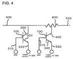
- FIG. 4is an equivalent circuit diagram of the semiconductor device illustrated in FIG. 1 to FIG. 3 ;
- FIGS. 5A to 5Care sectional views illustrating a method of manufacturing the semiconductor device illustrated in FIG. 1 to FIG. 3 ;
- FIG. 6is a sectional view explaining a configuration of a semiconductor device of a second embodiment
- FIG. 7is a sectional view explaining a configuration of a semiconductor device of a third embodiment
- FIG. 8is an equivalent circuit diagram of a protective circuit owned by the semiconductor device illustrated in FIG. 7 ;
- FIG. 9is a sectional view explaining a configuration of a semiconductor device of a fourth embodiment.
- FIG. 1is a plan view explaining a configuration of a semiconductor device of the first embodiment.
- the semiconductor devicehas a protective element.
- the protective elementhas a first-conductivity-type well 10 , a plurality of first diffusion layers 200 formed in the well 10 , a plurality of second diffusion layers 300 formed in the well 10 , and a diffusion resistance layer 400 formed in the well 10 .
- the first diffusion layers 200have a second conductivity type, and are connected in parallel with each other to an input/output terminal of the semiconductor device.
- the second diffusion layers 300are arranged alternately with the plurality of first diffusion layers 200 , and are connected to a power source or to the ground.
- the diffusion resistance layer 400has a second conductivity type, and is located in adjacent to any of the plurality of second diffusion layers 300 .
- the diffusion resistance layer 400is connected to the input/output terminal of the semiconductor device, while being arranged in parallel with the first diffusion layers 200 , and connects the internal circuit and the input/output terminal of the semiconductor device
- surge currentsuch as ascribable to static electricity
- the surge currentis allowed to discharge from the first diffusion layers 200 , through the well 10 and the second diffusion layers 300 , to a power source or to the ground.
- the diffusion resistance layer 400prevents the surge current to flow into the internal circuit. Since the diffusion resistance layer 400 is formed in the same well 10 in which the first diffusion layers 200 and the second diffusion layers are formed, and has the same conductivity type with the first diffusion layers 200 , so that part of the surge current may be discharged from the diffusion resistance layer 400 through the well 10 and the second diffusion layers 300 to the power source of to the ground.
- the protective elementmay be suppressed from being consequently lowered in the protection tolerance. Accordingly, the occupied area of the protective circuit (containing the protective element and resistors) may be reduced as compared with a configuration having an external resistor provided thereto, while assuming the protection tolerance of the both as identical. As a consequence, the semiconductor device may be suppressed from being enlarged. Details will be given below.
- the well 10 in this embodimenthas a square (or rectangular) form.
- the first diffusion layers 200 and the second diffusion layers 300have a nearly equivalent geometry, and are arranged at regular intervals to form a matrix, in the square (or rectangular) region of the well 10 .
- the diffusion resistance layer 400is arranged at one of four corners of the square region.
- the diffusion resistance layer 400has a rectangular geometry, having two edges thereof opposed with the first diffusion layers 200 and second diffusion layers 300 . More specifically, the diffusion resistance layer 400 is located in the vicinity of the edges which specify the outer circumference of the well 10 , and there are no first diffusion layers 200 and no second diffusion layers 300 located between these edges and the diffusion resistance layer 400 . The distance between the diffusion resistance layer 400 and each of all second diffusion layers 300 located in adjacent to the diffusion resistance layer 400 is equal to the distance between each of the first diffusion layers 200 and the second diffusion layers 300 adjacent to each other.
- Each of the first diffusion layers 200 and the second diffusion layers 300has a square form having an edge of 0.5 to 5 ⁇ m long, and is distant 0.1 to 1 ⁇ m away from each other.
- the area of the diffusion resistance layer 400is larger than the total area of one first diffusion layer 200 and one second diffusion layer 300 , and is typically 2 to 20 times as large as one first diffusion layers 200 .
- the length of oppositionwhich is expressed by the sum of the length of the portion where the first diffusion layers 200 and the second diffusion layers 300 are opposed with each other and the length of the portion where the first diffusion layers 200 and the diffusion resistance layer 400 are opposed with each other, may be reduced as compared with a configuration having the first diffusion layers 200 and the second diffusion layers 300 provided in place of the diffusion resistance layer 400 .
- the diffusion resistance layer 400is located in the vicinity of the edges which specify the outer circumference of the well 10 , and since there are no first diffusion layer 200 and the second diffusion layer 300 located between the diffusion resistance layer 400 and the edges closest to the diffusion resistance layer 400 . As a consequence, reduction in the length of opposition may be suppressed as compared with a configuration having the diffusion resistance layer 400 arranged deep inside the square region so as to make all of four edges thereof opposed with the first diffusion layers 200 and the second diffusion layers 300 .
- the square regionhaving the first diffusion layers 200 , the second diffusion layers 300 , and the diffusion resistance layer 400 arranged therein, is surrounded by a first-conductivity-type diffusion layer 100 .
- the diffusion layer 100is formed to draw a square pattern, and is provided in order to control potential of the well 10 .
- the edge closest to the diffusion resistance layer 400is away from the diffusion resistance layer 400 typically by a distance not larger than the width of the first diffusion layers 200 .
- FIG. 2is an enlarged view of a part of FIG. 1
- FIG. 3is a sectional view taken along line A-A′ in FIG. 2
- FIG. 4is an equivalent circuit diagram of the semiconductor device illustrated in FIG. 1 to FIG. 3 .
- the diffusion layer 100 , the first diffusion layers 200 , the second diffusion layers 300 , and the diffusion resistance layer 400are isolated from each other by a device isolation film 20 .
- the device isolation film 20is buried in a semiconductor layer 1 .
- the semiconductor layer 1may be a semiconductor substrate such as a silicon substrate, or may be a semiconductor layer of an SOI substrate.
- the diffusion layer 100is connected through silicide layers 110 and contacts 710 to an interconnect 510 of a first interconnect layer.
- the interconnect 510is connected to the ground.
- the interconnect 510is formed along the diffusion layer 100 , but is discontinued in the vicinity of the region over the diffusion resistance layer 400 . Through the discontinued portion, an interconnect 530 of the first interconnect layer, for connecting the protective element with the internal circuit, is extended.
- the first diffusion layers 200are connected through silicide layers 210 , contacts 740 , electro-conductive patterns 540 of the first interconnect layer, and vias 810 to an interconnect 600 of a second interconnect.
- the interconnect 600is connected to the input/output terminal, and covers, when viewed from the top of the semiconductor device, the square region having the first diffusion layers 200 , the second diffusion layers 300 , and the diffusion resistance layer 400 arranged therein.
- the second diffusion layers 300are connected through silicide layers 310 and contacts 720 to an interconnect 520 of the first interconnect.
- the interconnect 520is connected to the ground or the power source.
- the diffusion resistance layer 400is connected, in the vicinity of one shorter edge thereof, through silicide layers 410 , contacts 750 , electro-conductive patterns 550 of the first interconnect layer, and vias 820 to the interconnect 600 .
- the diffusion resistance layer 400is connected, in the vicinity of the other shorter edge thereof, through silicide layers 420 and contacts 730 to the interconnect 530 of the first interconnect.
- the silicide layers 410 , 420 located below the contacts 750 , 730are not connected with each other. Therefore, the diffusion resistance layer 400 may be suppressed from being lowered in the resistivity, so that the area of the diffusion resistance layer 400 may consequently be reduced.
- the resistivity of the diffusion resistance layer 400may be adjustable by adjusting the size of the silicide layers 410 , 420 , and thereby characteristics of the protective circuit may be adjustable.
- the first conductivity type in this embodimentis P-type
- the second conductivity typeis N-type
- the second diffusion layers 300have the second conductivity type, or N-type.
- the diffusion layer 100 , the well 10 , the first diffusion layers 200 , and the second diffusion layers 300compose a bipolar element as the protective element.
- the diffusion layer 100 , the well 10 , the diffusion resistance layer 400 , and the second diffusion layer 300compose a bipolar element as the protective element.
- the diffusion layer 100functions as the base
- the first diffusion layers 200 and the diffusion resistance layer 400function as the emitter
- the second diffusion layer 300functions as the collector.
- FIGS. 5A to 5Care sectional views illustrating a method of manufacturing the semiconductor device illustrated in FIG. 1 to FIG. 3 .
- the device isolation film 20 having the STI structureis formed in the semiconductor layer 1 .
- the depth of the device isolation film 20is typically 0.1 ⁇ m to 5 ⁇ m.
- the well 10is formed by ion implantation using a resist mask.
- a gate oxide film, gate electrodes, LDD regions, and side walls (all of which not illustrated) of CMOS transistors composing the internal circuitare formed.
- the diffusion layer 100 , the first diffusion layers 200 , the second diffusion layers 300 , and the diffusion resistance layer 400are formed by ion implantation using resist masks. In this process, also the sources and drains of the CMOS transistors are formed.
- a silicon oxide film 50is formed over the device isolation film 20 , the diffusion layer 100 , the first diffusion layers 200 , the second diffusion layers 300 , and the diffusion resistance layer 400 .
- a resist pattern 52is formed on the silicon oxide film 50 .
- the resist pattern 52covers a region of the diffusion resistance layer 400 where the silicide layers will not be formed therein later.
- the silicon oxide film 50is etched using the resist pattern 52 as a mask. By this process, the silicon oxide film 50 is removed, except for the region thereof where the silicide layers will not be formed therein later.
- the resist pattern 52is removed.
- a metal filmsuch as Ti film, Co film or the like, is formed over the diffusion layer 100 , the first diffusion layers 200 , the second diffusion layers 300 , the diffusion resistance layer 400 , and silicon oxide film 50 , and then annealed. By these processes, the silicide layers 110 , 210 , 310 , 410 and 420 are formed. The residual metal film is then removed.
- the insulating interlayer as the first layer, the contacts 710 to 750 , the first interconnect layer, the insulating interlayer as the second layer, the vias 810 , 820 , and the second interconnect layerare formed.
- the diffusion resistance layer 400is formed in the same well 10 in which the first diffusion layers 200 and the second diffusion layers 300 are formed, and has the same conductivity type with the first diffusion layers 200 , so that a part of surge current flown from the input/output terminal may be discharged from the diffusion resistance layer 400 , through the well 10 and the second diffusion layers 300 , to the power source or the ground. Accordingly, even if the area of the region, having the first diffusion layers 200 and the second diffusion layers 300 formed therein, becomes smaller due to provision of the diffusion resistance layer 400 in the well 10 , the protective element may be suppressed from being consequently lowered in the protection tolerance.
- the occupied area of the protective circuitmay be reduced as compared with a configuration having an external resistor provided thereto, while assuming the protection tolerance of the both as identical.
- the semiconductor devicemay therefore be suppressed from being enlarged. This effect may be particularly distinctive, when the distance between the diffusion resistance layer and the second diffusion layers 300 is nearly equal to the distance between the first diffusion layers 200 and the second diffusion layers 300 .
- the diffusion resistance layer 400is arranged at the corner of the square region having the first diffusion layers 200 and the second diffusion layers 300 arranged therein, and two edges thereof oppose to the first diffusion layers 200 and the second diffusion layers 300 . Accordingly, reduction in the length of opposition may be suppressed as compared with a configuration having the diffusion resistance layer 400 arranged deep inside the square region so as to make all of four edges thereof opposed to the first diffusion layers 200 and the second diffusion layers 300 .
- the silicide layers 410 , 420 over the diffusion resistance layer 400are not connected with each other. Accordingly, the diffusion resistance layer 400 may be suppressed from being lowered in resistivity, and the area of the diffusion resistance layer 400 may therefore be reduced.
- the resistivity of the diffusion resistance layer 400may be adjustable by adjusting the size of the silicide layers 410 , 420 , and thereby characteristics of the protective circuit may be adjustable.
- FIG. 6is a sectional view explaining a configuration of a semiconductor device of a second embodiment, and corresponds to FIG. 3 in the first embodiment.
- the semiconductor deviceis similar to that of the first embodiment, except that the well 10 and the diffusion layer 100 are N-type, and the first diffusion layers 200 , the second diffusion layers 300 , and the diffusion resistance layer 400 are P-type.
- the well 10 and the diffusion layer 100are N-type
- the first diffusion layers 200 , the second diffusion layers 300 , and the diffusion resistance layer 400are P-type.
- a method of manufacturing the semiconductor device of this embodimentis similar to as described in the first embodiment. Effects similar to those in the first embodiment may be obtainable also in this embodiment.
- FIG. 7is a sectional view explaining a configuration of a semiconductor device of a third embodiment, and corresponds to FIG. 3 in the first embodiment.
- This embodimentis similar to the first embodiment, except that the second diffusion layer 300 has the first conductivity type, similarly to the well 10 and the diffusion layer 100 .
- the first conductivity typeis P-type
- the second conductivity typeis N-type.
- FIG. 8is an equivalent circuit diagram of a protective circuit owned by the semiconductor device illustrated in FIG. 7 .
- the first diffusion layers 200 , the well 10 , and the second diffusion layers 300compose a diode as the protective element.
- the diffusion resistance layer 400 , the well 10 , and the second diffusion layers 300compose a diode as the protective element.
- the first diffusion layers 200 and the diffusion resistance layer 400function as the cathode, and the diffusion layer 100 and the second diffusion layers 300 function as the anode.
- a method of manufacturing the semiconductor device of this embodimentis similar to as described in the first embodiment. Effects similar to those in the first embodiment may be obtainable also in this embodiment.
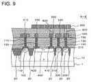
- FIG. 9is a sectional view explaining a configuration of a semiconductor device of a fourth embodiment.
- the semiconductor device of this embodimentis similar to that of the third embodiment, except that the well 10 , the diffusion layer 100 , and the second diffusion layers 300 are N-type, and the first diffusion layers 200 and the diffusion resistance layer 400 are P-type.
- the first diffusion layers 200 and the diffusion resistance layer 400function as the anode
- the diffusion layer 100 and the second diffusion layers 300function as the cathode.
- a method of manufacturing the semiconductor device of this embodimentis similar to as described in the first embodiment. Effects similar to those in the first embodiment may be obtainable also in this embodiment.
Landscapes
- Semiconductor Integrated Circuits (AREA)
- Metal-Oxide And Bipolar Metal-Oxide Semiconductor Integrated Circuits (AREA)
- Bipolar Integrated Circuits (AREA)
Abstract
Description
Claims (19)
Applications Claiming Priority (2)
| Application Number | Priority Date | Filing Date | Title |
|---|---|---|---|
| JP2008083700AJP5371274B2 (en) | 2008-03-27 | 2008-03-27 | Semiconductor device |
| JP2008-083700 | 2008-03-27 |
Publications (2)
| Publication Number | Publication Date |
|---|---|
| US20090242991A1 US20090242991A1 (en) | 2009-10-01 |
| US8008723B2true US8008723B2 (en) | 2011-08-30 |
Family
ID=41115795
Family Applications (1)
| Application Number | Title | Priority Date | Filing Date |
|---|---|---|---|
| US12/379,510Expired - Fee RelatedUS8008723B2 (en) | 2008-03-27 | 2009-02-24 | Semiconductor device including a plurality of diffusion layers and diffusion resistance layer |
Country Status (3)
| Country | Link |
|---|---|
| US (1) | US8008723B2 (en) |
| JP (1) | JP5371274B2 (en) |
| CN (1) | CN101546752B (en) |
Cited By (45)
| Publication number | Priority date | Publication date | Assignee | Title |
|---|---|---|---|---|
| US8644049B2 (en) | 2010-08-20 | 2014-02-04 | Shine C. Chung | Circuit and system of using polysilicon diode as program selector for one-time programmable devices |
| US8804398B2 (en) | 2010-08-20 | 2014-08-12 | Shine C. Chung | Reversible resistive memory using diodes formed in CMOS processes as program selectors |
| US8830720B2 (en) | 2010-08-20 | 2014-09-09 | Shine C. Chung | Circuit and system of using junction diode as program selector and MOS as read selector for one-time programmable devices |
| US8848423B2 (en) | 2011-02-14 | 2014-09-30 | Shine C. Chung | Circuit and system of using FinFET for building programmable resistive devices |
| US8861249B2 (en) | 2012-02-06 | 2014-10-14 | Shine C. Chung | Circuit and system of a low density one-time programmable memory |
| US8913415B2 (en) | 2010-08-20 | 2014-12-16 | Shine C. Chung | Circuit and system for using junction diode as program selector for one-time programmable devices |
| US8913449B2 (en) | 2012-03-11 | 2014-12-16 | Shine C. Chung | System and method of in-system repairs or configurations for memories |
| US8912576B2 (en) | 2011-11-15 | 2014-12-16 | Shine C. Chung | Structures and techniques for using semiconductor body to construct bipolar junction transistors |
| US8917533B2 (en) | 2012-02-06 | 2014-12-23 | Shine C. Chung | Circuit and system for testing a one-time programmable (OTP) memory |
| US8923085B2 (en) | 2010-11-03 | 2014-12-30 | Shine C. Chung | Low-pin-count non-volatile memory embedded in a integrated circuit without any additional pins for access |
| US8988965B2 (en) | 2010-11-03 | 2015-03-24 | Shine C. Chung | Low-pin-count non-volatile memory interface |
| US9007804B2 (en) | 2012-02-06 | 2015-04-14 | Shine C. Chung | Circuit and system of protective mechanisms for programmable resistive memories |
| US9019791B2 (en) | 2010-11-03 | 2015-04-28 | Shine C. Chung | Low-pin-count non-volatile memory interface for 3D IC |
| US9019742B2 (en) | 2010-08-20 | 2015-04-28 | Shine C. Chung | Multiple-state one-time programmable (OTP) memory to function as multi-time programmable (MTP) memory |
| US9025357B2 (en) | 2010-08-20 | 2015-05-05 | Shine C. Chung | Programmable resistive memory unit with data and reference cells |
| US9042153B2 (en) | 2010-08-20 | 2015-05-26 | Shine C. Chung | Programmable resistive memory unit with multiple cells to improve yield and reliability |
| US9070437B2 (en) | 2010-08-20 | 2015-06-30 | Shine C. Chung | Circuit and system of using junction diode as program selector for one-time programmable devices with heat sink |
| US9076526B2 (en) | 2012-09-10 | 2015-07-07 | Shine C. Chung | OTP memories functioning as an MTP memory |
| US9136261B2 (en) | 2011-11-15 | 2015-09-15 | Shine C. Chung | Structures and techniques for using mesh-structure diodes for electro-static discharge (ESD) protection |
| US9183897B2 (en) | 2012-09-30 | 2015-11-10 | Shine C. Chung | Circuits and methods of a self-timed high speed SRAM |
| US9224496B2 (en) | 2010-08-11 | 2015-12-29 | Shine C. Chung | Circuit and system of aggregated area anti-fuse in CMOS processes |
| US9236141B2 (en) | 2010-08-20 | 2016-01-12 | Shine C. Chung | Circuit and system of using junction diode of MOS as program selector for programmable resistive devices |
| US9251893B2 (en) | 2010-08-20 | 2016-02-02 | Shine C. Chung | Multiple-bit programmable resistive memory using diode as program selector |
| US9324447B2 (en) | 2012-11-20 | 2016-04-26 | Shine C. Chung | Circuit and system for concurrently programming multiple bits of OTP memory devices |
| US9324849B2 (en) | 2011-11-15 | 2016-04-26 | Shine C. Chung | Structures and techniques for using semiconductor body to construct SCR, DIAC, or TRIAC |
| US9412473B2 (en) | 2014-06-16 | 2016-08-09 | Shine C. Chung | System and method of a novel redundancy scheme for OTP |
| US9431127B2 (en) | 2010-08-20 | 2016-08-30 | Shine C. Chung | Circuit and system of using junction diode as program selector for metal fuses for one-time programmable devices |
| US9460807B2 (en) | 2010-08-20 | 2016-10-04 | Shine C. Chung | One-time programmable memory devices using FinFET technology |
| US9496033B2 (en) | 2010-08-20 | 2016-11-15 | Attopsemi Technology Co., Ltd | Method and system of programmable resistive devices with read capability using a low supply voltage |
| US9496265B2 (en) | 2010-12-08 | 2016-11-15 | Attopsemi Technology Co., Ltd | Circuit and system of a high density anti-fuse |
| US9711237B2 (en) | 2010-08-20 | 2017-07-18 | Attopsemi Technology Co., Ltd. | Method and structure for reliable electrical fuse programming |
| US9818478B2 (en) | 2012-12-07 | 2017-11-14 | Attopsemi Technology Co., Ltd | Programmable resistive device and memory using diode as selector |
| US9824768B2 (en) | 2015-03-22 | 2017-11-21 | Attopsemi Technology Co., Ltd | Integrated OTP memory for providing MTP memory |
| US10192615B2 (en) | 2011-02-14 | 2019-01-29 | Attopsemi Technology Co., Ltd | One-time programmable devices having a semiconductor fin structure with a divided active region |
| US10229746B2 (en) | 2010-08-20 | 2019-03-12 | Attopsemi Technology Co., Ltd | OTP memory with high data security |
| US10249379B2 (en) | 2010-08-20 | 2019-04-02 | Attopsemi Technology Co., Ltd | One-time programmable devices having program selector for electrical fuses with extended area |
| US10535413B2 (en) | 2017-04-14 | 2020-01-14 | Attopsemi Technology Co., Ltd | Low power read operation for programmable resistive memories |
| US10586832B2 (en) | 2011-02-14 | 2020-03-10 | Attopsemi Technology Co., Ltd | One-time programmable devices using gate-all-around structures |
| US10726914B2 (en) | 2017-04-14 | 2020-07-28 | Attopsemi Technology Co. Ltd | Programmable resistive memories with low power read operation and novel sensing scheme |
| US10770160B2 (en) | 2017-11-30 | 2020-09-08 | Attopsemi Technology Co., Ltd | Programmable resistive memory formed by bit slices from a standard cell library |
| US10916317B2 (en) | 2010-08-20 | 2021-02-09 | Attopsemi Technology Co., Ltd | Programmable resistance memory on thin film transistor technology |
| US10923204B2 (en) | 2010-08-20 | 2021-02-16 | Attopsemi Technology Co., Ltd | Fully testible OTP memory |
| US11062786B2 (en) | 2017-04-14 | 2021-07-13 | Attopsemi Technology Co., Ltd | One-time programmable memories with low power read operation and novel sensing scheme |
| US20220399717A1 (en)* | 2021-06-11 | 2022-12-15 | Semiconductor Components Industries, Llc | Interference filter and electrostatic discharge / electrical surge protection circuit and device |
| US11615859B2 (en) | 2017-04-14 | 2023-03-28 | Attopsemi Technology Co., Ltd | One-time programmable memories with ultra-low power read operation and novel sensing scheme |
Families Citing this family (1)
| Publication number | Priority date | Publication date | Assignee | Title |
|---|---|---|---|---|
| JP6393587B2 (en) | 2014-03-05 | 2018-09-19 | ローム株式会社 | Bidirectional Zener diode |
Citations (13)
| Publication number | Priority date | Publication date | Assignee | Title |
|---|---|---|---|---|
| US4757363A (en)* | 1984-09-14 | 1988-07-12 | Harris Corporation | ESD protection network for IGFET circuits with SCR prevention guard rings |
| JPH0270229A (en) | 1988-09-01 | 1990-03-09 | Mitsubishi Electric Corp | Input protection circuit for semiconductor integrated circuits |
| JPH06302765A (en) | 1993-04-13 | 1994-10-28 | Citizen Watch Co Ltd | Protective circuit of semiconductor device |
| US5374844A (en)* | 1993-03-25 | 1994-12-20 | Micrel, Inc. | Bipolar transistor structure using ballast resistor |
| JPH10150109A (en) | 1996-11-19 | 1998-06-02 | Nec Corp | Semi conductor device |
| US5936282A (en)* | 1994-04-13 | 1999-08-10 | Kabushiki Kaisha Toshiba | Semiconductor device having input protection circuit |
| US20040075529A1 (en)* | 2001-09-28 | 2004-04-22 | Agere Systems Inc., | High dopant conentration diffused resistor and method of manufacture therefor |
| US20040173867A1 (en)* | 2003-03-07 | 2004-09-09 | Beigel Kurt D. | Bulk-isolated PN diode and method of forming a bulk-isolated PN diode |
| JP2005109163A (en) | 2003-09-30 | 2005-04-21 | Nec Electronics Corp | Semiconductor element |
| US20060258067A1 (en)* | 2005-05-10 | 2006-11-16 | Samsung Electronics Co., Ltd. | Device for protecting against electrostatic discharge |
| US20070020818A1 (en)* | 2005-07-22 | 2007-01-25 | Mediatek Inc. | ESD protection device in high voltage and manufacturing method for the same |
| US20080029782A1 (en)* | 2006-08-04 | 2008-02-07 | Texas Instruments, Inc. | Integrated ESD protection device |
| US7408754B1 (en)* | 2004-11-18 | 2008-08-05 | Altera Corporation | Fast trigger ESD device for protection of integrated circuits |
Family Cites Families (5)
| Publication number | Priority date | Publication date | Assignee | Title |
|---|---|---|---|---|
| JPH04335570A (en)* | 1991-05-10 | 1992-11-24 | Hitachi Ltd | semiconductor equipment |
| US5384482A (en)* | 1992-05-18 | 1995-01-24 | Nec Corporation | Semiconductor integrated circuit device having input protective circuit |
| JP3161508B2 (en)* | 1996-07-25 | 2001-04-25 | 日本電気株式会社 | Semiconductor device |
| KR100214566B1 (en)* | 1997-04-22 | 1999-08-02 | 구본준 | Input protection circuit |
| JP5041749B2 (en)* | 2006-07-13 | 2012-10-03 | ルネサスエレクトロニクス株式会社 | Semiconductor device |
- 2008
- 2008-03-27JPJP2008083700Apatent/JP5371274B2/ennot_activeExpired - Fee Related
- 2009
- 2009-02-24USUS12/379,510patent/US8008723B2/ennot_activeExpired - Fee Related
- 2009-03-27CNCN2009101279406Apatent/CN101546752B/ennot_activeExpired - Fee Related
Patent Citations (13)
| Publication number | Priority date | Publication date | Assignee | Title |
|---|---|---|---|---|
| US4757363A (en)* | 1984-09-14 | 1988-07-12 | Harris Corporation | ESD protection network for IGFET circuits with SCR prevention guard rings |
| JPH0270229A (en) | 1988-09-01 | 1990-03-09 | Mitsubishi Electric Corp | Input protection circuit for semiconductor integrated circuits |
| US5374844A (en)* | 1993-03-25 | 1994-12-20 | Micrel, Inc. | Bipolar transistor structure using ballast resistor |
| JPH06302765A (en) | 1993-04-13 | 1994-10-28 | Citizen Watch Co Ltd | Protective circuit of semiconductor device |
| US5936282A (en)* | 1994-04-13 | 1999-08-10 | Kabushiki Kaisha Toshiba | Semiconductor device having input protection circuit |
| JPH10150109A (en) | 1996-11-19 | 1998-06-02 | Nec Corp | Semi conductor device |
| US20040075529A1 (en)* | 2001-09-28 | 2004-04-22 | Agere Systems Inc., | High dopant conentration diffused resistor and method of manufacture therefor |
| US20040173867A1 (en)* | 2003-03-07 | 2004-09-09 | Beigel Kurt D. | Bulk-isolated PN diode and method of forming a bulk-isolated PN diode |
| JP2005109163A (en) | 2003-09-30 | 2005-04-21 | Nec Electronics Corp | Semiconductor element |
| US7408754B1 (en)* | 2004-11-18 | 2008-08-05 | Altera Corporation | Fast trigger ESD device for protection of integrated circuits |
| US20060258067A1 (en)* | 2005-05-10 | 2006-11-16 | Samsung Electronics Co., Ltd. | Device for protecting against electrostatic discharge |
| US20070020818A1 (en)* | 2005-07-22 | 2007-01-25 | Mediatek Inc. | ESD protection device in high voltage and manufacturing method for the same |
| US20080029782A1 (en)* | 2006-08-04 | 2008-02-07 | Texas Instruments, Inc. | Integrated ESD protection device |
Cited By (68)
| Publication number | Priority date | Publication date | Assignee | Title |
|---|---|---|---|---|
| US9224496B2 (en) | 2010-08-11 | 2015-12-29 | Shine C. Chung | Circuit and system of aggregated area anti-fuse in CMOS processes |
| US9019742B2 (en) | 2010-08-20 | 2015-04-28 | Shine C. Chung | Multiple-state one-time programmable (OTP) memory to function as multi-time programmable (MTP) memory |
| US9236141B2 (en) | 2010-08-20 | 2016-01-12 | Shine C. Chung | Circuit and system of using junction diode of MOS as program selector for programmable resistive devices |
| US8760904B2 (en) | 2010-08-20 | 2014-06-24 | Shine C. Chung | One-Time Programmable memories using junction diodes as program selectors |
| US8804398B2 (en) | 2010-08-20 | 2014-08-12 | Shine C. Chung | Reversible resistive memory using diodes formed in CMOS processes as program selectors |
| US8817563B2 (en) | 2010-08-20 | 2014-08-26 | Shine C. Chung | Sensing circuit for programmable resistive device using diode as program selector |
| US8830720B2 (en) | 2010-08-20 | 2014-09-09 | Shine C. Chung | Circuit and system of using junction diode as program selector and MOS as read selector for one-time programmable devices |
| US10923204B2 (en) | 2010-08-20 | 2021-02-16 | Attopsemi Technology Co., Ltd | Fully testible OTP memory |
| US8854859B2 (en) | 2010-08-20 | 2014-10-07 | Shine C. Chung | Programmably reversible resistive device cells using CMOS logic processes |
| US10916317B2 (en) | 2010-08-20 | 2021-02-09 | Attopsemi Technology Co., Ltd | Programmable resistance memory on thin film transistor technology |
| US8873268B2 (en) | 2010-08-20 | 2014-10-28 | Shine C. Chung | Circuit and system of using junction diode as program selector for one-time programmable devices |
| US8913415B2 (en) | 2010-08-20 | 2014-12-16 | Shine C. Chung | Circuit and system for using junction diode as program selector for one-time programmable devices |
| US10249379B2 (en) | 2010-08-20 | 2019-04-02 | Attopsemi Technology Co., Ltd | One-time programmable devices having program selector for electrical fuses with extended area |
| US10229746B2 (en) | 2010-08-20 | 2019-03-12 | Attopsemi Technology Co., Ltd | OTP memory with high data security |
| US10127992B2 (en) | 2010-08-20 | 2018-11-13 | Attopsemi Technology Co., Ltd. | Method and structure for reliable electrical fuse programming |
| US9460807B2 (en) | 2010-08-20 | 2016-10-04 | Shine C. Chung | One-time programmable memory devices using FinFET technology |
| US8929122B2 (en) | 2010-08-20 | 2015-01-06 | Shine C. Chung | Circuit and system of using a junction diode as program selector for resistive devices |
| US9431127B2 (en) | 2010-08-20 | 2016-08-30 | Shine C. Chung | Circuit and system of using junction diode as program selector for metal fuses for one-time programmable devices |
| US8644049B2 (en) | 2010-08-20 | 2014-02-04 | Shine C. Chung | Circuit and system of using polysilicon diode as program selector for one-time programmable devices |
| US8760916B2 (en) | 2010-08-20 | 2014-06-24 | Shine C. Chung | Circuit and system of using at least one junction diode as program selector for memories |
| US9478306B2 (en) | 2010-08-20 | 2016-10-25 | Attopsemi Technology Co., Ltd. | Circuit and system of using junction diode as program selector for one-time programmable devices with heat sink |
| US9754679B2 (en) | 2010-08-20 | 2017-09-05 | Attopsemi Technology Co., Ltd | One-time programmable memory devices using FinFET technology |
| US9042153B2 (en) | 2010-08-20 | 2015-05-26 | Shine C. Chung | Programmable resistive memory unit with multiple cells to improve yield and reliability |
| US9070437B2 (en) | 2010-08-20 | 2015-06-30 | Shine C. Chung | Circuit and system of using junction diode as program selector for one-time programmable devices with heat sink |
| US9767915B2 (en) | 2010-08-20 | 2017-09-19 | Attopsemi Technology Co., Ltd | One-time programmable device with integrated heat sink |
| US9385162B2 (en) | 2010-08-20 | 2016-07-05 | Shine C. Chung | Programmably reversible resistive device cells using CMOS logic processes |
| US9025357B2 (en) | 2010-08-20 | 2015-05-05 | Shine C. Chung | Programmable resistive memory unit with data and reference cells |
| US9711237B2 (en) | 2010-08-20 | 2017-07-18 | Attopsemi Technology Co., Ltd. | Method and structure for reliable electrical fuse programming |
| US8649203B2 (en) | 2010-08-20 | 2014-02-11 | Shine C. Chung | Reversible resistive memory using polysilicon diodes as program selectors |
| US9349773B2 (en) | 2010-08-20 | 2016-05-24 | Shine C. Chung | Memory devices using a plurality of diodes as program selectors for memory cells |
| US9251893B2 (en) | 2010-08-20 | 2016-02-02 | Shine C. Chung | Multiple-bit programmable resistive memory using diode as program selector |
| US9496033B2 (en) | 2010-08-20 | 2016-11-15 | Attopsemi Technology Co., Ltd | Method and system of programmable resistive devices with read capability using a low supply voltage |
| US9305973B2 (en) | 2010-08-20 | 2016-04-05 | Shine C. Chung | One-time programmable memories using polysilicon diodes as program selectors |
| US9293220B2 (en) | 2010-11-03 | 2016-03-22 | Shine C. Chung | Low-pin-count non-volatile memory interface for 3D IC |
| US9281038B2 (en) | 2010-11-03 | 2016-03-08 | Shine C. Chung | Low-pin-count non-volatile memory interface |
| US9343176B2 (en) | 2010-11-03 | 2016-05-17 | Shine C. Chung | Low-pin-count non-volatile memory interface with soft programming capability |
| US9019791B2 (en) | 2010-11-03 | 2015-04-28 | Shine C. Chung | Low-pin-count non-volatile memory interface for 3D IC |
| US9076513B2 (en) | 2010-11-03 | 2015-07-07 | Shine C. Chung | Low-pin-count non-volatile memory interface with soft programming capability |
| US8923085B2 (en) | 2010-11-03 | 2014-12-30 | Shine C. Chung | Low-pin-count non-volatile memory embedded in a integrated circuit without any additional pins for access |
| US8988965B2 (en) | 2010-11-03 | 2015-03-24 | Shine C. Chung | Low-pin-count non-volatile memory interface |
| US9496265B2 (en) | 2010-12-08 | 2016-11-15 | Attopsemi Technology Co., Ltd | Circuit and system of a high density anti-fuse |
| US9881970B2 (en) | 2011-02-14 | 2018-01-30 | Attopsemi Technology Co. LTD. | Programmable resistive devices using Finfet structures for selectors |
| US11011577B2 (en) | 2011-02-14 | 2021-05-18 | Attopsemi Technology Co., Ltd | One-time programmable memory using gate-all-around structures |
| US9548109B2 (en) | 2011-02-14 | 2017-01-17 | Attopsemi Technology Co., Ltd | Circuit and system of using FinFET for building programmable resistive devices |
| US8848423B2 (en) | 2011-02-14 | 2014-09-30 | Shine C. Chung | Circuit and system of using FinFET for building programmable resistive devices |
| US10586832B2 (en) | 2011-02-14 | 2020-03-10 | Attopsemi Technology Co., Ltd | One-time programmable devices using gate-all-around structures |
| US10192615B2 (en) | 2011-02-14 | 2019-01-29 | Attopsemi Technology Co., Ltd | One-time programmable devices having a semiconductor fin structure with a divided active region |
| US8912576B2 (en) | 2011-11-15 | 2014-12-16 | Shine C. Chung | Structures and techniques for using semiconductor body to construct bipolar junction transistors |
| US9324849B2 (en) | 2011-11-15 | 2016-04-26 | Shine C. Chung | Structures and techniques for using semiconductor body to construct SCR, DIAC, or TRIAC |
| US9136261B2 (en) | 2011-11-15 | 2015-09-15 | Shine C. Chung | Structures and techniques for using mesh-structure diodes for electro-static discharge (ESD) protection |
| US8861249B2 (en) | 2012-02-06 | 2014-10-14 | Shine C. Chung | Circuit and system of a low density one-time programmable memory |
| US9007804B2 (en) | 2012-02-06 | 2015-04-14 | Shine C. Chung | Circuit and system of protective mechanisms for programmable resistive memories |
| US8917533B2 (en) | 2012-02-06 | 2014-12-23 | Shine C. Chung | Circuit and system for testing a one-time programmable (OTP) memory |
| US8913449B2 (en) | 2012-03-11 | 2014-12-16 | Shine C. Chung | System and method of in-system repairs or configurations for memories |
| US9076526B2 (en) | 2012-09-10 | 2015-07-07 | Shine C. Chung | OTP memories functioning as an MTP memory |
| US9183897B2 (en) | 2012-09-30 | 2015-11-10 | Shine C. Chung | Circuits and methods of a self-timed high speed SRAM |
| US9324447B2 (en) | 2012-11-20 | 2016-04-26 | Shine C. Chung | Circuit and system for concurrently programming multiple bits of OTP memory devices |
| US9818478B2 (en) | 2012-12-07 | 2017-11-14 | Attopsemi Technology Co., Ltd | Programmable resistive device and memory using diode as selector |
| US10586593B2 (en) | 2012-12-07 | 2020-03-10 | Attopsemi Technology Co., Ltd | Programmable resistive device and memory using diode as selector |
| US9412473B2 (en) | 2014-06-16 | 2016-08-09 | Shine C. Chung | System and method of a novel redundancy scheme for OTP |
| US9824768B2 (en) | 2015-03-22 | 2017-11-21 | Attopsemi Technology Co., Ltd | Integrated OTP memory for providing MTP memory |
| US10726914B2 (en) | 2017-04-14 | 2020-07-28 | Attopsemi Technology Co. Ltd | Programmable resistive memories with low power read operation and novel sensing scheme |
| US10535413B2 (en) | 2017-04-14 | 2020-01-14 | Attopsemi Technology Co., Ltd | Low power read operation for programmable resistive memories |
| US11062786B2 (en) | 2017-04-14 | 2021-07-13 | Attopsemi Technology Co., Ltd | One-time programmable memories with low power read operation and novel sensing scheme |
| US11615859B2 (en) | 2017-04-14 | 2023-03-28 | Attopsemi Technology Co., Ltd | One-time programmable memories with ultra-low power read operation and novel sensing scheme |
| US10770160B2 (en) | 2017-11-30 | 2020-09-08 | Attopsemi Technology Co., Ltd | Programmable resistive memory formed by bit slices from a standard cell library |
| US20220399717A1 (en)* | 2021-06-11 | 2022-12-15 | Semiconductor Components Industries, Llc | Interference filter and electrostatic discharge / electrical surge protection circuit and device |
| US12316105B2 (en)* | 2021-06-11 | 2025-05-27 | Semiconductor Components Industries, Llc | Interference filter and electrostatic discharge / electrical surge protection circuit and device |
Also Published As
| Publication number | Publication date |
|---|---|
| JP2009239049A (en) | 2009-10-15 |
| JP5371274B2 (en) | 2013-12-18 |
| CN101546752A (en) | 2009-09-30 |
| CN101546752B (en) | 2011-08-10 |
| US20090242991A1 (en) | 2009-10-01 |
Similar Documents
| Publication | Publication Date | Title |
|---|---|---|
| US8008723B2 (en) | Semiconductor device including a plurality of diffusion layers and diffusion resistance layer | |
| US7465995B2 (en) | Resistor structure for ESD protection circuits | |
| JP4854934B2 (en) | Electrostatic discharge protection element | |
| JP3237110B2 (en) | Semiconductor device | |
| JP4209432B2 (en) | ESD protection device | |
| US9548292B2 (en) | Circuit including a resistive element, a diode, and a switch and a method of using the same | |
| JP5041749B2 (en) | Semiconductor device | |
| JP4209433B2 (en) | ESD protection device | |
| US20050133839A1 (en) | Semiconductor device | |
| US8754479B2 (en) | Semiconductor device | |
| JP2010182727A (en) | Semiconductor device | |
| JP2008091687A (en) | Semiconductor integrated circuit device | |
| US10700053B2 (en) | Electrostatic protection element | |
| JP2006339444A (en) | Semiconductor device and method for manufacturing the same | |
| US9343558B1 (en) | Silicon controlled rectifier | |
| US20200328592A1 (en) | Electrostatic discharge protection device | |
| US8618584B2 (en) | Semiconductor device | |
| JP4645069B2 (en) | Semiconductor device | |
| JP2005294634A (en) | Semiconductor device and manufacturing method thereof | |
| JP5297495B2 (en) | Electrostatic discharge protection element | |
| JP2009187987A (en) | Semiconductor device | |
| JP2012028380A (en) | Semiconductor device | |
| JP2007019413A (en) | Semiconductor device for protection circuit | |
| JP2007059543A (en) | ESD protection circuit and ESD protection circuit manufacturing method | |
| JP2006005028A (en) | Semiconductor protective device |
Legal Events
| Date | Code | Title | Description |
|---|---|---|---|
| AS | Assignment | Owner name:NEC ELECTRONICS CORPORATION, JAPAN Free format text:ASSIGNMENT OF ASSIGNORS INTEREST;ASSIGNOR:NAGAI, TAKAYUKI;REEL/FRAME:022353/0964 Effective date:20090213 | |
| AS | Assignment | Owner name:RENESAS ELECTRONICS CORPORATION, JAPAN Free format text:CHANGE OF NAME;ASSIGNOR:NEC ELECTRONICS CORPORATION;REEL/FRAME:025214/0187 Effective date:20100401 | |
| STCF | Information on status: patent grant | Free format text:PATENTED CASE | |
| FEPP | Fee payment procedure | Free format text:PAYOR NUMBER ASSIGNED (ORIGINAL EVENT CODE: ASPN); ENTITY STATUS OF PATENT OWNER: LARGE ENTITY | |
| FPAY | Fee payment | Year of fee payment:4 | |
| AS | Assignment | Owner name:RENESAS ELECTRONICS CORPORATION, JAPAN Free format text:CHANGE OF ADDRESS;ASSIGNOR:RENESAS ELECTRONICS CORPORATION;REEL/FRAME:044928/0001 Effective date:20150806 | |
| FEPP | Fee payment procedure | Free format text:MAINTENANCE FEE REMINDER MAILED (ORIGINAL EVENT CODE: REM.); ENTITY STATUS OF PATENT OWNER: LARGE ENTITY | |
| LAPS | Lapse for failure to pay maintenance fees | Free format text:PATENT EXPIRED FOR FAILURE TO PAY MAINTENANCE FEES (ORIGINAL EVENT CODE: EXP.); ENTITY STATUS OF PATENT OWNER: LARGE ENTITY | |
| STCH | Information on status: patent discontinuation | Free format text:PATENT EXPIRED DUE TO NONPAYMENT OF MAINTENANCE FEES UNDER 37 CFR 1.362 | |
| FP | Lapsed due to failure to pay maintenance fee | Effective date:20190830 |