US8008710B2 - Non-volatile semiconductor storage device - Google Patents
Non-volatile semiconductor storage deviceDownload PDFInfo
- Publication number
- US8008710B2 US8008710B2US12/501,142US50114209AUS8008710B2US 8008710 B2US8008710 B2US 8008710B2US 50114209 AUS50114209 AUS 50114209AUS 8008710 B2US8008710 B2US 8008710B2
- Authority
- US
- United States
- Prior art keywords
- storage device
- semiconductor storage
- columnar portions
- memory
- layer
- Prior art date
- Legal status (The legal status is an assumption and is not a legal conclusion. Google has not performed a legal analysis and makes no representation as to the accuracy of the status listed.)
- Active, expires
Links
Images


Classifications
- H—ELECTRICITY
- H10—SEMICONDUCTOR DEVICES; ELECTRIC SOLID-STATE DEVICES NOT OTHERWISE PROVIDED FOR
- H10B—ELECTRONIC MEMORY DEVICES
- H10B43/00—EEPROM devices comprising charge-trapping gate insulators
- H10B43/20—EEPROM devices comprising charge-trapping gate insulators characterised by three-dimensional arrangements, e.g. with cells on different height levels
- G—PHYSICS
- G11—INFORMATION STORAGE
- G11C—STATIC STORES
- G11C16/00—Erasable programmable read-only memories
- G11C16/02—Erasable programmable read-only memories electrically programmable
- G11C16/04—Erasable programmable read-only memories electrically programmable using variable threshold transistors, e.g. FAMOS
- G11C16/0483—Erasable programmable read-only memories electrically programmable using variable threshold transistors, e.g. FAMOS comprising cells having several storage transistors connected in series
- G—PHYSICS
- G11—INFORMATION STORAGE
- G11C—STATIC STORES
- G11C5/00—Details of stores covered by group G11C11/00
- G11C5/02—Disposition of storage elements, e.g. in the form of a matrix array
- G—PHYSICS
- G11—INFORMATION STORAGE
- G11C—STATIC STORES
- G11C5/00—Details of stores covered by group G11C11/00
- G11C5/02—Disposition of storage elements, e.g. in the form of a matrix array
- G11C5/025—Geometric lay-out considerations of storage- and peripheral-blocks in a semiconductor storage device
- G—PHYSICS
- G11—INFORMATION STORAGE
- G11C—STATIC STORES
- G11C5/00—Details of stores covered by group G11C11/00
- G11C5/06—Arrangements for interconnecting storage elements electrically, e.g. by wiring
- G11C5/063—Voltage and signal distribution in integrated semi-conductor memory access lines, e.g. word-line, bit-line, cross-over resistance, propagation delay
- G—PHYSICS
- G11—INFORMATION STORAGE
- G11C—STATIC STORES
- G11C8/00—Arrangements for selecting an address in a digital store
- G11C8/14—Word line organisation; Word line lay-out
- H—ELECTRICITY
- H10—SEMICONDUCTOR DEVICES; ELECTRIC SOLID-STATE DEVICES NOT OTHERWISE PROVIDED FOR
- H10B—ELECTRONIC MEMORY DEVICES
- H10B43/00—EEPROM devices comprising charge-trapping gate insulators
- H10B43/10—EEPROM devices comprising charge-trapping gate insulators characterised by the top-view layout
- H—ELECTRICITY
- H10—SEMICONDUCTOR DEVICES; ELECTRIC SOLID-STATE DEVICES NOT OTHERWISE PROVIDED FOR
- H10B—ELECTRONIC MEMORY DEVICES
- H10B43/00—EEPROM devices comprising charge-trapping gate insulators
- H10B43/20—EEPROM devices comprising charge-trapping gate insulators characterised by three-dimensional arrangements, e.g. with cells on different height levels
- H10B43/23—EEPROM devices comprising charge-trapping gate insulators characterised by three-dimensional arrangements, e.g. with cells on different height levels with source and drain on different levels, e.g. with sloping channels
- H10B43/27—EEPROM devices comprising charge-trapping gate insulators characterised by three-dimensional arrangements, e.g. with cells on different height levels with source and drain on different levels, e.g. with sloping channels the channels comprising vertical portions, e.g. U-shaped channels
- H—ELECTRICITY
- H10—SEMICONDUCTOR DEVICES; ELECTRIC SOLID-STATE DEVICES NOT OTHERWISE PROVIDED FOR
- H10D—INORGANIC ELECTRIC SEMICONDUCTOR DEVICES
- H10D30/00—Field-effect transistors [FET]
- H10D30/60—Insulated-gate field-effect transistors [IGFET]
- H10D30/69—IGFETs having charge trapping gate insulators, e.g. MNOS transistors
- H10D30/693—Vertical IGFETs having charge trapping gate insulators
- H—ELECTRICITY
- H10—SEMICONDUCTOR DEVICES; ELECTRIC SOLID-STATE DEVICES NOT OTHERWISE PROVIDED FOR
- H10D—INORGANIC ELECTRIC SEMICONDUCTOR DEVICES
- H10D30/00—Field-effect transistors [FET]
- H10D30/60—Insulated-gate field-effect transistors [IGFET]
- H10D30/69—IGFETs having charge trapping gate insulators, e.g. MNOS transistors
- H10D30/694—IGFETs having charge trapping gate insulators, e.g. MNOS transistors characterised by the shapes, relative sizes or dispositions of the gate electrodes
- H10D30/697—IGFETs having charge trapping gate insulators, e.g. MNOS transistors characterised by the shapes, relative sizes or dispositions of the gate electrodes having trapping at multiple separated sites, e.g. multi-particles trapping sites
- H—ELECTRICITY
- H10—SEMICONDUCTOR DEVICES; ELECTRIC SOLID-STATE DEVICES NOT OTHERWISE PROVIDED FOR
- H10D—INORGANIC ELECTRIC SEMICONDUCTOR DEVICES
- H10D62/00—Semiconductor bodies, or regions thereof, of devices having potential barriers
- H10D62/10—Shapes, relative sizes or dispositions of the regions of the semiconductor bodies; Shapes of the semiconductor bodies
- H10D62/124—Shapes, relative sizes or dispositions of the regions of semiconductor bodies or of junctions between the regions
- H10D62/125—Shapes of junctions between the regions
Definitions
- the present inventionrelates to an electrically rewritable non-volatile semiconductor storage device.
- LSIsare formed by integration of devices in a two-dimensional plane on the silicon substrate.
- it is common to reduce (refine) the dimension for each device for increased memory storage capacityrecent years are facing challenges in such refinement from the viewpoint of cost and technology.
- Such refinementrequires further improvements in photolithography technology.
- the costs of lithography processare ever increasing.
- physical improvement limitsuch as in breakdown voltage between devices, would be reached unless driving voltage can be scaled. That is, it is likely that difficulties would be encountered in device operation itself.
- One of the conventional semiconductor storage devices where memory cells are arranged in a three-dimensional manneruses transistors with a cylinder-type structure.
- Those semiconductor storage devices using transistors with the cylinder-type structureare provided with multiple conductive layers corresponding to gate electrodes and pillar-like columnar semiconductors.
- Each of the columnar semiconductorsserves as a channel (body) part of each of the transistors.
- Memory gate insulation layersare provided around the columnar semiconductors. Such a configuration including these conductive layers, columnar semiconductors, and memory gate insulation layers is referred to as a “memory string”.
- source linesshould be formed on the bottom surface of the lamination structure, and their contacts should also be formed with trenches dug down to the bottom surface of the lamination structure.
- source linesare highly doped with impurities for lowering resistance. To mitigate thermal diffusion of impurities from the source lines while keeping good contact resistance with such source lines, sensitive interface control is required for different thermal processes.
- such a three-dimensional type non-volatile semiconductor storage devicehas been disclosed in, e.g., Japanese Patent Laid-Open No. 2007-317874, where memory strings are formed in U-shape, enabling both bit lines and source lines to be formed on the surface of the lamination structure.
- Japanese Patent Laid-Open No. 2007-317874requires word lines to be formed separately for each memory string, which poses a problem that the wiring resistance of the word lines cannot be reduced.
- One aspect of the present inventionprovides a non-volatile semiconductor storage device comprising a plurality of memory strings, each having a plurality of electrically rewritable memory cells and selection transistors connected in series, each of the memory strings comprising: a semiconductor layer having a plurality of columnar portion and a joining portion, the plurality of columnar portions extending in a vertical direction with respect to a substrate, the joining portion being formed to join lower ends of the plurality of columnar portions with a first direction taken as a longitudinal direction; an electric charge storage layer formed to surround side surfaces of the columnar portions; a plurality of first conductive layers formed in a laminated fashion to surround side surfaces of the columnar portions and the electric charge storage layer, the first conductive layers functioning as control electrodes of the memory cells; a second conductive layer formed around the plurality of columnar portions aligned in the first direction via a gate insulation film, with the first direction taken as a longitudinal direction, the second conductive layer functioning as control electrodes of the selection transistors; and bit lines formed to be
- FIG. 1is a schematic diagram of a non-volatile semiconductor storage device 100 according to a first embodiment of the present invention
- FIG. 2is a perspective view schematically illustrating a part of the memory transistor area 12 in the non-volatile semiconductor storage device 100 according to the first embodiment
- FIG. 3is an equivalent circuit diagram of one memory string MS
- FIG. 4is a plan view of the memory transistor area 12 ;
- FIG. 5is a cross-sectional view taken along the line A-A′ of FIG. 4 ;
- FIG. 6is an enlarged view of a part of FIG. 5 ;
- FIG. 7is a cross-sectional view taken along the line B-B′ of FIG. 4 ;
- FIG. 8is a process diagram illustrating a method of manufacturing the non-volatile semiconductor storage device 100 according to the first embodiment
- FIG. 9is a process diagram illustrating a method of manufacturing the non-volatile semiconductor storage device 100 according to the first embodiment
- FIG. 10is a process diagram illustrating a method of manufacturing the non-volatile semiconductor storage device 100 according to the first embodiment
- FIG. 11is a process diagram illustrating a method of manufacturing the non-volatile semiconductor storage device 100 according to the first embodiment
- FIG. 12is a process diagram illustrating a method of manufacturing the non-volatile semiconductor storage device 100 according to the first embodiment
- FIG. 13is a process diagram illustrating a method of manufacturing the non-volatile semiconductor storage device 100 according to the first embodiment
- FIG. 14is a process diagram illustrating a method of manufacturing the non-volatile semiconductor storage device 100 according to the first embodiment
- FIG. 15is an equivalent circuit diagram illustrating a write operation of the non-volatile semiconductor storage device 100 according to the first embodiment
- FIG. 16is an equivalent circuit diagram illustrating a read operation of the non-volatile semiconductor storage device 100 according to the first embodiment
- FIG. 17is a schematic diagram of the memory transistor area 12 in the non-volatile semiconductor storage device 100 according to a second embodiment of the present invention.
- FIG. 18is a plan view of the memory transistor area 12 in the non-volatile semiconductor storage device 100 according to the second embodiment of the present invention.
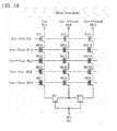
- FIG. 1schematically illustrates a non-volatile semiconductor storage device 100 according to a first embodiment of the present invention.
- the non-volatile semiconductor storage device 100 according to the first embodimentmainly comprises: a memory transistor area 12 ; a word-line driving circuit 13 ; a selection gate line driving circuit 15 ; a sense amplifier 16 ; and a back-gate transistor driving circuit 18 .
- the memory transistor area 12has memory transistors for storing data.
- the memory transistorsare connected in series to provide memory strings, as discussed below.
- selection transistorsare connected to the opposite ends of the memory strings.
- the word-line driving circuit 13controls voltage applied to word lines WL.
- the selection gate line driving circuit 15controls voltage applied to selection gate lines SG.
- the sense amplifier 16amplifies a potential read from a memory transistor.
- the back-gate transistor driving circuit 18controls voltage applied to a back-gate line BG described below.
- the non-volatile semiconductor storage device 100according to the first embodiment comprises a bit-line driving circuit (not illustrated) for controlling voltage applied to bit lines BL.
- FIG. 2is a perspective view schematically illustrating a part of the memory transistor area 12 in the non-volatile semiconductor storage device 100 according to the first embodiment.
- the memory transistor area 12has memory strings MS arranged in the form of m ⁇ n matrix on a substrate Ba (where m and n are natural numbers), each memory string including a plurality of memory transistors MC and selection transistors SG.
- each memory string MShas a plurality of electrically rewritable memory transistors MC connected in series and parallel (so as to form a W-shape).
- the memory transistors MC included in a memory string MSare formed and arranged in a three-dimensional manner on the substrate Ba by laminating multiple semiconductor layers.
- Each memory string MShas a W-shaped semiconductor layer SC mn , word lines WL 1 to WL 4 , and a selection gate line SG.
- the memory strings MShave a back-gate line BG.
- Each W-shaped semiconductor layer SC mnis formed in a W-shape form (sideways E-shape or comb-like form) as viewed from the row direction.
- Each W-shaped semiconductor layer SC mnhas a plurality of (three, in this case) columnar portions CL mn extending in substantially the vertical direction with respect to the semiconductor substrate Ba, and a joining portion JP mn formed to join the lower ends of the respective columnar portions CL mn .
- the joining portion JP mnis formed with the column direction illustrated in FIG. 2 taken as the longitudinal direction.
- the three columnar portions CL mn included in one memory string MSare also formed in line along the column direction.
- an electric charge storage layerwhich is a part of a memory cell, is formed around the plurality of columnar portions CL mn via a tunnel insulation film as described below, and a block insulation film is further formed around the electric charge storage layer.
- word lines WL 1 to WL 4are formed around the plurality of columnar portions CL mn via the tunnel insulation film, the electric charge storage layer, and the block insulation film.
- the word lines WL 1 to WL 4are formed by laminating multiple layers of conductive films on the substrate Ba via an interlayer insulation film, not illustrated in FIG. 2 .
- the word lines WL 1 to WL 4are formed as plate-like electrodes that are commonly connected to m ⁇ n memory strings MS arranged in a two-dimensional manner and in a grid pattern on the substrate Ba. Because of the plate-like shapes commonly connected to the memory strings arranged in a matrix form, instead of being formed in an elongated stripe pattern (in strips) per memory strings arranged in a line, the word lines WL 1 to WL 4 may provide a lower wiring resistance as compared with being formed in an elongated stripe pattern.
- the selection gate lines SGare commonly connected to a plurality of columnar portions CL mn aligned in the column direction so that they provide a stripe pattern on the tip sides of the columnar portions CL mn , with the column direction taken as the longitudinal direction. That is, a plurality of memory strings MS aligned in the row direction are each connected to different selection gate lines SG 1 , SG 2 , and SG 3 .
- the back-gate line BGcomes in contact with the joining portion JP mn via a gate insulation film, not illustrated.
- Each joining portion JP mnhas two back gate transistors BT formed therein, with their gate electrodes included in the back-gate line BG.
- bit lines BLare formed along the columnar portions CL mn aligned in the row direction, with the row direction taken as the longitudinal direction.
- Three columnar portions CLmn 1 to CLmn 3 included in one memory string MSare each connected to different bit lines BL 0 to BL 2 .
- FIG. 3is an equivalent circuit diagram of one memory string MS.
- This memory string MShas four memory cells MC formed therein for each columnar portion CL mn , and a total of 12 (4 ⁇ 3) memory cells MC for three columnar portions CLmn 1 to CLmn 3 .
- the left columnar portion CL mn 1has memory transistors MC 1 to MC 4 formed therein.
- the middle columnar portion CL mn 2has memory transistors MC 5 to MC 8 formed therein.
- the right columnar portion CL mn 3has memory transistors MC 9 to MC 12 formed therein.
- the memory transistors MC 1 , MC 5 , andMC 9are commonly connected to the word line WL 1 in the lowest layer closest to the substrate Ba.
- the memory transistors MC 2 , MC 6 , and MC 10are commonly connected to the word line WL 2 in the second lowest layer.
- the memory transistors MC 3 , MC 7 , and MC 11are commonly connected to the word line WL 3 in the third lowest layer.
- the memory transistors MC 4 , MC 8 , and MC 12are commonly connected to the word line WL 4 in the highest layer.
- the joining portion JP mnhas two back gate transistors BT 1 and BT 2 that are formed at respective positions between three columnar portions CL mn 1 to CL mn 3 , with their gates included in the back gate layer BG.
- those memory transistors MC that are formed along at least one of three columnar portions CL mnare always kept at an erase state (where data “ 1 ” is retained) by a write/erase control circuit, not illustrated (herein, an “erase state” means that the memory cell MC is normally kept in a conductive state irrespective of voltages that may be applied to a control electrode thereof.
- At least one of the sets of four memory transistors, each formed along one columnar portion CL mnwill be always kept at an erase state. Specifically, at least one set (four memory transistors) will be kept at an erase state, among the sets of memory transistors MC 1 to MC 4 , MC 5 to MC 8 , and MC 9 to MC 12 .
- This measureis taken because write and read operations may still be performed when the word lines WL with a plate-like structure are utilized as described above, which will be discussed in detail below.
- the following descriptionis based on the assumption that the memory transistors MC 5 to MC 8 connected to the middle columnar portion CLmn 2 are always kept at erase states.
- selection transistors ST 1 to ST 3are formed on the upper ends of the plurality of columnar portions CL mn .
- the selection transistors ST 1 to ST 3are commonly connected to one selection gate line SG and become conductive at the same time.
- Such memory strings MSare arranged in a two-dimensional matrix form on the substrate Ba, with the word lines WL 1 to WL 4 being connected in common.
- the columnar portions CL mnmay be columnar or prismatic in shape.
- the columnar portions CL mnmay also be terraced columnar shape.
- the word lines WL 1 to WL 4have their column-direction ends formed in a stepwise manner in relation to each other for contact purpose.
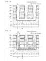
- FIG. 4is a plan view of the memory transistor area 12 ;
- FIG. 5is a cross-sectional view taken along the line A-A′ of FIG. 4 ;
- FIG. 6is a partial enlarged view thereof;
- FIG. 7is a cross-sectional view taken along the line B-B′ of FIG. 4 .
- bit lines BLare formed in the memory cell transistor area 12 , with the row direction taken as the longitudinal direction, and with a wiring width of 2 F and wiring pitch of 3 F (where F denotes a minimum resolution width).
- Selection gate lines CGare also formed therein, with the column direction taken as the longitudinal direction, and with a wiring width of 2 F and wiring pitch of 3 F, as well.
- the above-mentioned columnar portions CLmn 1 to CLmn 3are formed at respective intersections between the bit lines BL and the selection gate lines CG so as to penetrate near the center of their intersecting positions.
- the memory cell transistor area 12(one memory string MS) has a back gate transistor layer 20 , a memory transistor layer 30 , a selection transistor layer 40 , and a wiring layer 50 , in order from the semiconductor substrate Ba to the lamination direction.
- the back gate transistor layer 20functions as the above-mentioned back gate transistor BG, and has a surface on which the joining portion JP mn of a W-shaped semiconductor layer SC mn is formed.
- the memory transistor layer 30functions as the above-mentioned memory transistors MC.
- the selection transistor layer 40functions as the above-mentioned selection transistors SG.
- the wiring layer 50has bit lines BL formed therein.
- the back gate transistor layer 20has a back gate interlayer insulation layer 21 and a back gate conductive layer 22 corresponding to the back-gate line BG, which layers are sequentially laminated on the semiconductor substrate Ba.
- the back gate interlayer insulation layer 21 and the back gate conductive layer 22are formed to expand to the ends of the memory transistor area 12 in the row and column directions.
- the back gate conductive layer 22is formed to cover the bottom and side surfaces of the joining portion JP mn , and as high as the top surface thereof.
- the back gate interlayer insulation layer 21is composed of silicon oxide (SiO 2 ).
- the back gate conductive layer 22is composed of polysilicon (p-Si).
- the memory transistor layer 30has first to fifth insulation layers between word lines 31 a to 31 e and first to fourth word-line conductive layers 32 a to 32 d that are alternately laminated on the back gate conductive layer 22 .
- the latterare conductive layers corresponding to the above-mentioned word lines WL 1 to WL 4 , while the former are interlayer insulation films deposited between the word lines WL 1 to WL 4 .
- the memory transistor layer 30also has memory protection insulation layers 34 that are deposited on the fourth insulation layers between word lines 31 e.
- the first to fifth insulation layers between word lines 31 a to 31 eare composed of silicon oxide (SiO 2 ).
- the first to fourth word-line conductive layers 32 a to 32 dare composed of polysilicon (p-Si).
- the memory protection insulation layers 34are composed of silicon nitride (SiN).
- the first to fifth insulation layers between word lines 31 a to 31 e and the first to fourth word-line conductive layers 32 a to 32 dare processed in a stepwise manner in relation to each other for connection to the contacts at their column-direction ends, as illustrated in FIG. 1 .
- the memory protection insulation layers 34are formed to cover the respective row- and column-direction ends of the first to fifth insulation layers between word lines 31 a to 31 e and the first to fourth word-line conductive layers 32 a to 32 d.
- the above-mentioned columnar portions CLmn 1 to CLmn 3are formed within three memory holes 35 a that are provided to penetrate the first to fifth insulation layers between word lines 31 a to 31 e and the first to fourth word-line conductive layers 32 a to 32 d .
- the above-mentioned joining portion JP mnis further formed within a back gate hole 24 that is formed on the surface of the back gate transistor layer 20 below the memory holes 35 a . As a result, a W-shaped semiconductor layer SC mn is formed.
- each ONO film 62includes a block insulation layer BI, an electric charge storage layer EC, and a tunnel insulation layer TI deposited therein in the stated order as viewed from the word line side.
- Each block insulation layer BIis composed of silicon oxide (SiO 2 ).
- Each electric charge storage layer ECis composed of silicon nitride (SiN) and accumulates electric charges for retaining data.
- Each tunnel insulation layer TIis composed of silicon oxide (SiO 2 ). This means that the memory gate insulation layers 62 are composed of ONO layers and function as electric charge storage layers for accumulating electric charges.
- a conductive film 63is formed within the back gate hole 24 and the memory holes 35 a via the ONO films 62 .
- the conductive film 63has a hollow therein, and an internal insulation layer 64 is formed to fill the hollow.
- the W-shaped semiconductor layer SC mnis formed with the conductive film 63 and the internal insulation layer 64 .
- the selection transistor layer 40has selection-gate-line conductive layers 41 and interlayer insulation layers 44 that are formed on the memory protection insulation layers 34 .
- the selection-gate-line conductive layers 41function as the above-mentioned selection gate lines SG.
- the selection-gate-line conductive layers 41 and the interlayer insulation layers 44are formed in repeated lines such that extend in the column direction as the longitudinal direction and with a predetermined interval F in the row direction.
- the selection-gate-line conductive layers 41are composed of polysilicon (p-Si).
- the interlayer insulation layers 44are composed of silicon oxide (SiO 2 ).
- the selection transistor layer 40has selection-transistor-side holes 45 that are formed to penetrate the interlayer insulation layers 44 and the selection-gate-line conductive layers 41 .
- the selection-transistor-side holes 45are formed at positions matching the memory holes 35 a.
- gate insulation layers 65are formed on the sidewalls facing the selection-transistor-side holes 45 .
- Conductive films 67are formed to fill the holes 45 via the gate insulation layers 65 .
- the gate insulation layers 65are composed of silicon oxide (SiO 2 ), and the conductive films 67 are formed by polysilicon.
- the gate insulation layers 65function as the gate insulation films of the selection transistors SG.
- the conductive films 67function as the channel parts of the selection transistors SG and constitute parts of the respective columnar portions CL mn .
- the wiring layer 50has first wiring insulation layers 51 , second wiring insulation layers 52 , contact layers 53 , and bit-line conductive layers 55 that are sequentially laminated on the selection transistor insulation layers 44 .
- the first and second wiring insulation layers 51 and 52are composed of silicon oxide (SiO 2 ).
- the contact layers 53are embedded in trenches that are formed to dig into the first wiring insulation layers 51 .
- the bit-line conductive layers 55are embedded in trenches that are formed to dig into the second wiring insulation layers 52 .
- the bit-line conductive layers 55are composed of, e.g., tantalum (Ta)-tantalum nitride (TaN)-copper (Cu). As illustrated in FIGS. 5 and 7 , one bit-line conductive layer 55 is provided for each columnar portion CL mn , with the row direction taken as the longitudinal direction.
- columnar portions CL mnare not connected by a joining portion JP mn in the row direction, as illustrated in FIG. 7 , and they belong to independent memory strings MS, respectively.
- FIGS. 8 to 14a method of manufacturing the non-volatile semiconductor storage device 100 according to the first embodiment will be described below.
- the memory transistor area 12 and a peripheral circuit areaare formed at the same time, the following description only focuses the manufacturing process of the memory transistor area 12 in relation to the features of this embodiment for simplicity.
- silicon oxide (SiO 2 ) and polysilicon (p-Si)are first deposited on the semiconductor substrate, and then a back gate interlayer insulation layer 21 and a back gate conductive layer 22 are formed in the memory transistor area 12 with the lithography method, RIE (Reactive Ion Etching) method, ion injection method, and the like.
- the back gate conductive layer 22is dug down to a depth in the memory transistor area 12 to form a back gate hole 24 .
- the back gate hole 24is formed in such a way that it has the width direction in the row direction and the longitudinal direction in the column direction, and has an insular aperture for each memory string MS. Such back gate holes 24 are formed at a predetermined interval in the row and column directions.
- silicon nitride (SiN)is deposited to fill the back gate hole 24 as a sacrificial film.
- silicon nitride (SiN) located on the upper portion of the back gate conductive layer 22is removed by the Chemical Mechanical Polishing (CMP) or RIE method to form a sacrificial layer 91 in the back gate hole 24 .
- CMPChemical Mechanical Polishing
- back gate hole 24is formed to such a depth that does not penetrate the back gate conductive layer 22 as illustrated in FIG. 9 , it may be formed to penetrate the back gate conductive layer 22 .
- silicon oxide (SiO 2 ) and polysilicon (p-Si)are alternately laminated on the back gate conductive layer 22 and the sacrificial layer 91 to form first to fifth insulation layers between word lines 31 a ′ to 31 e ′ and first to fourth polysilicon conductive layers 32 a ′ to 32 d ′.
- memory holes 35 aare formed to penetrate the first to fifth insulation layers between word lines 31 a ′ to 31 e ′ and the first to fourth polysilicon layers 32 a ′ to 32 d′.
- the memory holes 35 aare formed at respective positions near the opposite ends in the column direction, and near the center of the back gate hole 24 , respectively. That is, the three memory holes 35 a and the back gate hole 24 together form a W-shape.
- the sacrificial layer 91is removed as illustrated in FIG. 11 .
- removal of the sacrificial layer 91is performed in a hot phosphoric acid solution.
- a diluted hydrofluoric acid treatmentis performed to clean up, and remove any natural oxide film from, the exposed surfaces of the back gate conductive layer 22 and the first to fourth polysilicon layers 32 a ′ to 32 d ′, respectively.
- a memory gate insulation layer 62is formed to cover the respective sidewalls facing the back gate hole 24 and the memory hole 35 a .
- a memory gate insulation layer 62is formed on the sidewalls as an ONO film by sequentially depositing silicon oxide (SiO 2 ), silicon nitride (SiN), and silicon oxide (SiO 2 ).
- amorphous silicon(a-Si) is deposited in the W-shaped void including the memory hole 35 a and the back gate hole 24 to form an amorphous silicon layer 93 .
- the amorphous silicon layer 93is formed to have a hollow 93 a .
- the amorphous silicon layer 93is formed in such a way that it will not completely fill the back gate hole 24 and the memory hole 35 a.
- the sidewalls of the amorphous silicon layer 93 facing the hollow 93 aare thermally oxidized to form silicon oxide (SiO 2 ).
- the remaining portions of the amorphous silicon layer 93are crystallized to form polysilicon (p-Si) thereby forming a W-shaped conductive film 63 .
- silicon oxide (SiO 2 )is further deposited on the silicon oxide (SiO 2 ) formed in the hollow 93 a of the W-shaped semiconductor layer 63 with the CVD (Chemical Vapor Deposition) method, and an internal insulation layer 64 is formed to fill the hollow 93 a.
- those portions of the memory gate insulation layer 62 , the conductive layer 63 , and the internal insulation layer 64are removed by CMP process that are deposited on the insulation layer between word lines 31 e′.
- a selection transistor layer 40a wiring layer 50 , a peripheral circuit area, and a contact area are generated according to the method as disclosed in, e.g., an earlier Japanese patent application, Laid-Open No. 2007-266143, filed by the same applicant, whereby the non-volatile semiconductor storage device 100 is manufactured as illustrated in FIG. 1 .
- a write operation to the memory transistor MC 2 in a memory string MSwill be described below.
- the voltage of all bit lines BL 0 to BL 2is set to the ground potential VSS, and the voltage of the back-gate line BG is set to the ground potential Vss, whereby back gate transistors BT 1 and BT 2 are kept at non-conducting states.
- the voltage of the selection gates SGis also set to the ground voltage Vss, and thus the selection transistors ST 1 to ST 3 are also kept at non-conducting states.
- a predetermined voltage Vgis applied to the selection gate SG connected to the memory string MS in which the memory transistor MC 2 is positioned, whereby the selection transistors ST 1 to ST 3 are set to conducting states.
- the voltage Vgis not applied to other selection gates SG connected to non-selected memory strings MS that are not written, and thus the body potential (channel potential: the potential of the columnar portions CL mn ) of the non-selected memory strings MS is kept at a floating state.
- bit line BL 1 connected to the memory transistor MC 2 to be writtenremains at the ground potential Vss
- the remaining bit lines BL 0 and BL 2are raised to a predetermined bit-line voltage V B .
- the body potential of the memory cells MC 5 to MC 12 that are not writtenis isolated from the bit lines BL and set to a floating state, preventing any write to these memory cells.
- the body potential of the columnar portion CLmn 1 in which the memory transistor MC 2 to be written is positionedwill be fixed to the ground voltage VSS.
- each word line WL 1 to WL 4is raised to as high as a voltage Vpass (on the order of 8V) that causes the memory transistor MC to become conducting without write, and then the voltage of the word line WL 2 to which the memory transistor MC 2 to be written to is connected is further raised to a write voltage Vpgm (20V or more). In this way, data is written to the desired memory transistor MC 2 .
- Vpasson the order of 8V
- individual write controlmay be achieved over memory transistors by setting the back gate transistors BT 1 and BT 2 to non-conducting states (OFF) and isolating the memory transistors MC 1 to MC 4 along the columnar portion CLmn 1 from the memory transistors MC 9 to MC 12 along the columnar portion CLmn 2 . That is, even if the bit-line voltage for write operation is applied to ones of the memory transistors, the others will not be affected since that voltage will not be applied thereto.
- the write operationmay also be performed on a memory transistor along the columnar portion CLmn 3 in a similar manner. This merely requires the bit line BL 2 to be set to the ground voltage Vss and the bit line BL 1 to a predetermined voltage V B .
- the voltage of all bit lines BL 0 to BL 2 , the selection gate lines SG, the word lines WL 1 to WL 4 , and the back-gate line BGare once lowered to the ground voltage Vss, and the potential then begins to increase for raising the voltage of the bit lines BL 0 to BL 2 toward an erase voltage Verase.
- the potential of the selection gate lines SGis raised from the ground voltage Vss to the predetermined voltage V G for the purpose of preventing the gate insulation layers 65 of the selection transistors ST from reaching a dielectric breakdown voltage.
- the body potentialis eventually raised to near the erase voltage Verase. With the electric field caused by the body potential and the voltage Vss of the word lines WL, data is erased from the entire memory transistors in the block including the memory string MS.
- the erase operationmay be performed by applying the erase voltage Verase to only some of three bit lines BL 0 to BL 2 connected to one memory string MS, while isolating other bit lines from the sense amplifier circuit and keeping them at floating states.
- the back gate transistors BT 1 and BT 2may be kept at non-conducting states, the holes generated through the back gate transistors BT 1 and BT 2 should be injected into the channel part (body) of the memory string MS.
- bit lines BL 0 to BL 2are set to the ground voltage Vss and the voltage of the back-gate line BG is set to a predetermined voltage V BG , whereby back gate transistors BT 1 and BT 2 are set to conducting states (ON).
- the voltage of the selection gate lines SGis set to the ground voltage Vss, and the selection transistors ST 1 to ST 3 are then turned OFF.
- the bit lines BL 0 and BL 2are provisionally set to the voltage Vdread.
- the voltage of the word line WL 2 connected to the control gate of the memory transistor MC 2 to be readis set to the ground voltage Vss, while the voltage of the other word lines WL 1 , 3 , and 4 is set to a read voltage Vread.
- the read voltage Vreadhas a value greater than the threshold voltage of the memory transistor MC after data is written thereto. Accordingly, the memory transistor MC 2 to be read becomes conductive for data “ 1 ” and non-conductive for data “ 0 ”.
- other memory transistors MC without readingare set to conducting states, irrespective of whether the retaining data is “ 0 ” or “ 1 ”.
- the memory cells MC 5 to MC 8 along the columnar portion CLmn 2are always in erase states, and thus at least memory transistors MC 5 to MC 8 become conducting whenever the voltage Vdread is applied to the bit lines BL 0 and BL 2 , the ground voltage Vss is applied to the bit line BL 1 , and these voltages are further applied to the word lines WL 1 to WL 4 .
- the voltage for data readmay also be supplied to the memory cells MC 1 to MC 4 via the selection transistor ST 2 , the memory transistors MC 5 to MC 8 , and the back gate transistor BT 1 (the voltage of the back-gate line BG may be raised to near the voltage Vdread).
- data in the memory cell MC 2may be read by sensing the potential of the bit line BL 1 at a sense amplifier.
- the non-volatile semiconductor storage device 100 according to the first embodimentmay achieve high integration.
- each layer corresponding to respective memory transistors MC and selection transistor layers STmay be manufactured in a predetermined number of lithography steps, irrespective of the number of laminated word lines WL. That is, the non-volatile semiconductor storage device 100 may be manufactured at a lower cost.
- the non-volatile semiconductor storage device 100has a back-gate line BG in contact with a joining portion JP mn of a W-shaped semiconductor layer SC mn .
- the back-gate line BGfunctions as a back gate transistor BG for forming a channel in the joining portion JP mn . Therefore, a memory string MS with a good conducting property may be provided at a W-shaped semiconductor layer SC mn in a nearly non-doped state.
- this embodimentutilizes the memory strings MS formed in a W-shape, there will be no need to form any contacts below the memory transistor layer 30 . Consequently, the manufacturing process may be simplified and an improved degree of freedom may be obtained for the design of the memory transistor layers, which may result in a more reliable non-volatile semiconductor storage device. In addition, this embodiment does not require any source-line wiring and involves a small number of wiring layers correspondingly, which may reduce the manufacturing costs.
- this embodimentuses one of three bit lines BL 0 to BL 2 connected to one memory string MS as if it were a source line, which allows the respective bit lines BL 0 to BL 2 to have the same resistance and to be formed in the same wiring layer. Also in this sense, reduced manufacturing costs and improved reliability may be achieved.
- FIG. 17schematically illustrates the memory transistor area 12 in the non-volatile semiconductor storage device 100 according to a second embodiment of the present invention.
- FIG. 18is a plan view thereof. Note that the same reference numerals represent the same components as the first embodiment and description thereof will be omitted below.
- the odd-numbered selection gate lines SG 1 , SG 3 , SG 5 , and SG 7are formed in lower layers, and the even-numbered selection gate lines SG 2 , SG 4 , SG 6 , and SG 8 are formed at positions in between, and above, the respective odd-numbered selection gate lines.
- the two-layer alternating type selection gate line structure as mentioned aboveallows the area to be 4 F 2 for each columnar portion CL mn .
- the number of columnar portions CL mn included in one memory string MSis not limited to three, but may be any number not less than two.
- a relation between the number of columnar portions CL mn included in one memory string MS and the effective area of the columnar portions in which memory transistors are formedis as follows:
- the effective area of the columnar portions CL mncan be smaller, which may contribute to higher memory density.
- such a compound containing a metal elementsuch as a silicon layer or a metal film (such as aluminum), with its surface being silicided through reaction with metal such as cobalt, may be used for, e.g., the columnar portion CL mn 2 along the memory transistors MC 5 to MC 8 in which data is always kept at an erase state.
- a metal elementsuch as a silicon layer or a metal film (such as aluminum)
- metalsuch as cobalt
- high-concentration impuritiessuch as phosphorus
- This measurementmay reduce the voltage drop, ensuring more reliable read operations.
- the present inventionis not limited to this configuration and may not provide such memory transistors MC that are always kept at erase states.
- the potential of the selected word line WLneeds to be set higher than the ground potential Vss, and the amount of the read current can possibly be reduced to, in a worst case, about one half of that in the first embodiment, data can be read using a sense amplifier with a sufficient sensitivity and appropriate measures against noise. This allows for more effective use of cell arrays, and the area of columnar portions can be made 4 F 2 , irrespective of the number of columnar portions included in one memory string MS, contributing to higher density of semiconductor memory devices.
Landscapes
- Engineering & Computer Science (AREA)
- Microelectronics & Electronic Packaging (AREA)
- Semiconductor Memories (AREA)
- Non-Volatile Memory (AREA)
Abstract
Description
Claims (20)
Applications Claiming Priority (2)
| Application Number | Priority Date | Filing Date | Title |
|---|---|---|---|
| JP2008-207655 | 2008-08-12 | ||
| JP2008207655AJP5288936B2 (en) | 2008-08-12 | 2008-08-12 | Nonvolatile semiconductor memory device |
Publications (2)
| Publication Number | Publication Date |
|---|---|
| US20100038703A1 US20100038703A1 (en) | 2010-02-18 |
| US8008710B2true US8008710B2 (en) | 2011-08-30 |
Family
ID=41680700
Family Applications (1)
| Application Number | Title | Priority Date | Filing Date |
|---|---|---|---|
| US12/501,142Active2030-02-03US8008710B2 (en) | 2008-08-12 | 2009-07-10 | Non-volatile semiconductor storage device |
Country Status (4)
| Country | Link |
|---|---|
| US (1) | US8008710B2 (en) |
| JP (1) | JP5288936B2 (en) |
| KR (1) | KR101031699B1 (en) |
| TW (1) | TWI400792B (en) |
Cited By (180)
| Publication number | Priority date | Publication date | Assignee | Title |
|---|---|---|---|---|
| US20110002178A1 (en)* | 2009-07-06 | 2011-01-06 | Sung-Min Hwang | Vertical non-volatile memory device, method of fabricating the same device, and electric-electronic system having the same device |
| US20110018050A1 (en)* | 2009-07-21 | 2011-01-27 | Kabushiki Kaisha Toshiba | Nonvolatile semiconductor memory device and method for manufacturing same |
| US20110063916A1 (en)* | 2009-09-14 | 2011-03-17 | Kabushiki Kaisha Toshiba | Non-volatile semiconductor storage device |
| US20120001252A1 (en)* | 2010-06-30 | 2012-01-05 | Sandisk Corporation | Ultrahigh density vertical nand memory device and method of making thereof |
| US8193054B2 (en) | 2010-06-30 | 2012-06-05 | SanDisk Technologies, Inc. | Ultrahigh density vertical NAND memory device and method of making thereof |
| US8198672B2 (en) | 2010-06-30 | 2012-06-12 | SanDisk Technologies, Inc. | Ultrahigh density vertical NAND memory device |
| US8349681B2 (en) | 2010-06-30 | 2013-01-08 | Sandisk Technologies Inc. | Ultrahigh density monolithic, three dimensional vertical NAND memory device |
| US20130075805A1 (en)* | 2011-09-22 | 2013-03-28 | Kabushiki Kaisha Toshiba | Method for manufacturing nonvolatile semiconductor storage device and nonvolatile semiconductor storage device |
| US8614126B1 (en) | 2012-08-15 | 2013-12-24 | Sandisk Technologies Inc. | Method of making a three-dimensional memory array with etch stop |
| US8658499B2 (en) | 2012-07-09 | 2014-02-25 | Sandisk Technologies Inc. | Three dimensional NAND device and method of charge trap layer separation and floating gate formation in the NAND device |
| US8828884B2 (en) | 2012-05-23 | 2014-09-09 | Sandisk Technologies Inc. | Multi-level contact to a 3D memory array and method of making |
| US20140284691A1 (en)* | 2013-03-22 | 2014-09-25 | Kabushiki Kaisha Toshiba | Method for manufacturing semiconductor memory device and semiconductor memory device |
| US8847302B2 (en) | 2012-04-10 | 2014-09-30 | Sandisk Technologies Inc. | Vertical NAND device with low capacitance and silicided word lines |
| US20140291798A1 (en)* | 2011-06-28 | 2014-10-02 | Kabushiki Kaisha Toshiba | Semiconductor memory device |
| US8853767B2 (en) | 2012-06-04 | 2014-10-07 | SK Hynix Inc. | Three dimensional semiconductor memory device and method of manufacturing the same |
| US8878278B2 (en) | 2012-03-21 | 2014-11-04 | Sandisk Technologies Inc. | Compact three dimensional vertical NAND and method of making thereof |
| US8884357B2 (en) | 2013-03-12 | 2014-11-11 | Sandisk Technologies Inc. | Vertical NAND and method of making thereof using sequential stack etching and landing pad |
| US8928061B2 (en) | 2010-06-30 | 2015-01-06 | SanDisk Technologies, Inc. | Three dimensional NAND device with silicide containing floating gates |
| US8946023B2 (en) | 2013-03-12 | 2015-02-03 | Sandisk Technologies Inc. | Method of making a vertical NAND device using sequential etching of multilayer stacks |
| US8987087B2 (en) | 2013-07-08 | 2015-03-24 | Sandisk Technologies Inc. | Three dimensional NAND device with birds beak containing floating gates and method of making thereof |
| US8987089B1 (en) | 2013-09-17 | 2015-03-24 | Sandisk Technologies Inc. | Methods of fabricating a three-dimensional non-volatile memory device |
| US8987908B2 (en) | 2012-11-14 | 2015-03-24 | SK Hynix Inc. | Semiconductor memory device including a slit |
| US9023719B2 (en) | 2013-09-17 | 2015-05-05 | Sandisk Technologies Inc. | High aspect ratio memory hole channel contact formation |
| US9093480B2 (en) | 2013-04-01 | 2015-07-28 | Sandisk Technologies Inc. | Spacer passivation for high aspect ratio etching of multilayer stacks for three dimensional NAND device |
| US9099496B2 (en) | 2013-04-01 | 2015-08-04 | Sandisk Technologies Inc. | Method of forming an active area with floating gate negative offset profile in FG NAND memory |
| US9105736B2 (en) | 2009-03-19 | 2015-08-11 | Samsung Electronics Co., Ltd. | Three-dimensional nonvolatile memory devices including interposed floating gates |
| US9129861B2 (en) | 2012-10-05 | 2015-09-08 | Samsung Electronics Co., Ltd. | Memory device |
| US9130054B2 (en) | 2012-07-31 | 2015-09-08 | Samsung Electronics Co., Ltd. | Semiconductor memory devices and methods of fabricating the same |
| US9136130B1 (en) | 2014-08-11 | 2015-09-15 | Sandisk Technologies Inc. | Three dimensional NAND string with discrete charge trap segments |
| US9159739B2 (en) | 2010-06-30 | 2015-10-13 | Sandisk Technologies Inc. | Floating gate ultrahigh density vertical NAND flash memory |
| US9177966B1 (en) | 2014-07-08 | 2015-11-03 | Sandisk Technologies Inc. | Three dimensional NAND devices with air gap or low-k core |
| US9177613B2 (en) | 2012-09-05 | 2015-11-03 | Samsung Electronics Co., Ltd. | Semiconductor device |
| US20150348984A1 (en)* | 2014-05-30 | 2015-12-03 | SanDisk Technologies, Inc. | Method of making a monolithic three dimensional nand string using a select gate etch stop layer |
| US9224747B2 (en) | 2014-03-26 | 2015-12-29 | Sandisk Technologies Inc. | Vertical NAND device with shared word line steps |
| US9230983B1 (en) | 2014-08-20 | 2016-01-05 | Sandisk Technologies Inc. | Metal word lines for three dimensional memory devices |
| US9230987B2 (en) | 2014-02-20 | 2016-01-05 | Sandisk Technologies Inc. | Multilevel memory stack structure and methods of manufacturing the same |
| US9230905B2 (en) | 2014-01-08 | 2016-01-05 | Sandisk 3D Llc | Trench multilevel contact to a 3D memory array and method of making thereof |
| US9230974B1 (en) | 2014-08-26 | 2016-01-05 | Sandisk Technologies Inc. | Methods of selective removal of blocking dielectric in NAND memory strings |
| US9230980B2 (en) | 2013-09-15 | 2016-01-05 | Sandisk Technologies Inc. | Single-semiconductor-layer channel in a memory opening for a three-dimensional non-volatile memory device |
| US9230979B1 (en) | 2014-10-31 | 2016-01-05 | Sandisk Technologies Inc. | High dielectric constant etch stop layer for a memory structure |
| US9236396B1 (en) | 2014-11-12 | 2016-01-12 | Sandisk Technologies Inc. | Three dimensional NAND device and method of making thereof |
| US9236392B1 (en) | 2014-08-26 | 2016-01-12 | Sandisk Technologies Inc. | Multiheight electrically conductive via contacts for a multilevel interconnect structure |
| US9244865B2 (en)* | 2014-05-28 | 2016-01-26 | SanDisk Technologies, Inc. | Obtaining diagnostic information through host interfaces |
| US9257572B2 (en) | 2012-10-05 | 2016-02-09 | Samsung Electronics Co., Ltd. | Vertical type memory device |
| US9287167B2 (en) | 2012-10-05 | 2016-03-15 | Samsung Electronics Co., Ltd. | Vertical type memory device |
| US9305932B2 (en) | 2014-06-30 | 2016-04-05 | Sandisk Technologies Inc. | Methods of making three dimensional NAND devices |
| US9305849B1 (en) | 2014-11-12 | 2016-04-05 | Sandisk Technologies Inc. | Method of making a three dimensional NAND device |
| US9305934B1 (en) | 2014-10-17 | 2016-04-05 | Sandisk Technologies Inc. | Vertical NAND device containing peripheral devices on epitaxial semiconductor pedestal |
| US9331088B2 (en) | 2014-03-25 | 2016-05-03 | Sandisk 3D Llc | Transistor device with gate bottom isolation and method of making thereof |
| US9331094B2 (en) | 2014-04-30 | 2016-05-03 | Sandisk Technologies Inc. | Method of selective filling of memory openings |
| US9343507B2 (en) | 2014-03-12 | 2016-05-17 | Sandisk 3D Llc | Dual channel vertical field effect transistor including an embedded electrode |
| US9356043B1 (en) | 2015-06-22 | 2016-05-31 | Sandisk Technologies Inc. | Three-dimensional memory devices containing memory stack structures with position-independent threshold voltage |
| US9356031B2 (en) | 2014-08-11 | 2016-05-31 | Sandisk Technologies Inc. | Three dimensional NAND string memory devices with voids enclosed between control gate electrodes |
| US9356034B1 (en) | 2015-02-05 | 2016-05-31 | Sandisk Technologies Inc. | Multilevel interconnect structure and methods of manufacturing the same |
| US9362298B2 (en)* | 2014-09-11 | 2016-06-07 | Kabushiki Kaisha Toshiba | Non-volatile semiconductor memory device and manufacturing method thereof |
| US9379124B2 (en) | 2014-06-25 | 2016-06-28 | Sandisk Technologies Inc. | Vertical floating gate NAND with selectively deposited ALD metal films |
| US9397046B1 (en) | 2015-04-29 | 2016-07-19 | Sandisk Technologies Llc | Fluorine-free word lines for three-dimensional memory devices |
| US9397093B2 (en) | 2013-02-08 | 2016-07-19 | Sandisk Technologies Inc. | Three dimensional NAND device with semiconductor, metal or silicide floating gates and method of making thereof |
| US9397107B2 (en) | 2014-06-30 | 2016-07-19 | Sandisk Technologies Llc | Methods of making three dimensional NAND devices |
| US9401309B2 (en) | 2014-08-26 | 2016-07-26 | Sandisk Technologies Llc | Multiheight contact via structures for a multilevel interconnect structure |
| US9406814B2 (en) | 2013-07-30 | 2016-08-02 | Kabushiki Kaisha Toshiba | Non-volatile memory device |
| US9419012B1 (en) | 2015-06-19 | 2016-08-16 | Sandisk Technologies Llc | Three-dimensional memory structure employing air gap isolation |
| US9419058B1 (en) | 2015-02-05 | 2016-08-16 | Sandisk Technologies Llc | Memory device with comb-shaped electrode having a plurality of electrode fingers and method of making thereof |
| US20160240554A1 (en)* | 2007-12-11 | 2016-08-18 | Kabushiki Kaisha Toshiba | Non-volatile semiconductor storage device and method of manufacturing the same |
| US9431419B2 (en) | 2014-09-12 | 2016-08-30 | Kabushiki Kaisha Toshiba | Semiconductor memory device and method for manufacturing same |
| US9437606B2 (en) | 2013-07-02 | 2016-09-06 | Sandisk Technologies Llc | Method of making a three-dimensional memory array with etch stop |
| US9443861B1 (en) | 2015-05-28 | 2016-09-13 | Sandisk Technologies Llc | Fluorine-blocking insulating spacer for backside contact structure of three-dimensional memory structures |
| US9449987B1 (en) | 2015-08-21 | 2016-09-20 | Sandisk Technologies Llc | Three dimensional memory device with epitaxial semiconductor pedestal for peripheral transistors |
| US9449983B2 (en) | 2013-12-19 | 2016-09-20 | Sandisk Technologies Llc | Three dimensional NAND device with channel located on three sides of lower select gate and method of making thereof |
| US9449982B2 (en) | 2013-03-12 | 2016-09-20 | Sandisk Technologies Llc | Method of making a vertical NAND device using a sacrificial layer with air gap and sequential etching of multilayer stacks |
| US9455263B2 (en) | 2014-06-27 | 2016-09-27 | Sandisk Technologies Llc | Three dimensional NAND device with channel contacting conductive source line and method of making thereof |
| US9484296B2 (en) | 2015-02-12 | 2016-11-01 | Sandisk Technologies Llc | Self-aligned integrated line and via structure for a three-dimensional semiconductor device |
| US9496419B2 (en) | 2014-11-25 | 2016-11-15 | Sandisk Technologies Llc | Ruthenium nucleation layer for control gate electrodes in a memory structure |
| US9502471B1 (en) | 2015-08-25 | 2016-11-22 | Sandisk Technologies Llc | Multi tier three-dimensional memory devices including vertically shared bit lines |
| US9515085B2 (en) | 2014-09-26 | 2016-12-06 | Sandisk Technologies Llc | Vertical memory device with bit line air gap |
| US9524779B2 (en) | 2014-06-24 | 2016-12-20 | Sandisk Technologies Llc | Three dimensional vertical NAND device with floating gates |
| US9530785B1 (en) | 2015-07-21 | 2016-12-27 | Sandisk Technologies Llc | Three-dimensional memory devices having a single layer channel and methods of making thereof |
| US9530788B2 (en) | 2015-03-17 | 2016-12-27 | Sandisk Technologies Llc | Metallic etch stop layer in a three-dimensional memory structure |
| US9543318B1 (en) | 2015-08-21 | 2017-01-10 | Sandisk Technologies Llc | Three dimensional memory device with epitaxial semiconductor pedestal for peripheral transistors |
| US9553100B2 (en) | 2014-12-04 | 2017-01-24 | Sandisk Techologies Llc | Selective floating gate semiconductor material deposition in a three-dimensional memory structure |
| US9553146B2 (en) | 2014-06-05 | 2017-01-24 | Sandisk Technologies Llc | Three dimensional NAND device having a wavy charge storage layer |
| US9552991B2 (en) | 2014-04-30 | 2017-01-24 | Sandisk Technologies Llc | Trench vertical NAND and method of making thereof |
| US20170025438A1 (en) | 2012-06-04 | 2017-01-26 | SK Hynix Inc. | Semiconductor device |
| US9570455B2 (en) | 2014-11-25 | 2017-02-14 | Sandisk Technologies Llc | Metal word lines for three dimensional memory devices |
| US9570460B2 (en) | 2014-07-29 | 2017-02-14 | Sandisk Technologies Llc | Spacer passivation for high-aspect ratio opening film removal and cleaning |
| US9576975B2 (en) | 2014-08-26 | 2017-02-21 | Sandisk Technologies Llc | Monolithic three-dimensional NAND strings and methods of fabrication thereof |
| US9576966B1 (en) | 2015-09-21 | 2017-02-21 | Sandisk Technologies Llc | Cobalt-containing conductive layers for control gate electrodes in a memory structure |
| US9583615B2 (en) | 2015-02-17 | 2017-02-28 | Sandisk Technologies Llc | Vertical transistor and local interconnect structure |
| US9583539B2 (en) | 2014-08-19 | 2017-02-28 | Sandisk Technologies Llc | Word line connection for memory device and method of making thereof |
| US9589981B2 (en) | 2015-06-15 | 2017-03-07 | Sandisk Technologies Llc | Passive devices for integration with three-dimensional memory devices |
| US9589839B1 (en) | 2016-02-01 | 2017-03-07 | Sandisk Technologies Llc | Method of reducing control gate electrode curvature in three-dimensional memory devices |
| US9595535B1 (en) | 2016-02-18 | 2017-03-14 | Sandisk Technologies Llc | Integration of word line switches with word line contact via structures |
| US9601502B2 (en) | 2014-08-26 | 2017-03-21 | Sandisk Technologies Llc | Multiheight contact via structures for a multilevel interconnect structure |
| US9601508B2 (en) | 2015-04-27 | 2017-03-21 | Sandisk Technologies Llc | Blocking oxide in memory opening integration scheme for three-dimensional memory structure |
| US9613977B2 (en) | 2015-06-24 | 2017-04-04 | Sandisk Technologies Llc | Differential etch of metal oxide blocking dielectric layer for three-dimensional memory devices |
| US9620512B1 (en) | 2015-10-28 | 2017-04-11 | Sandisk Technologies Llc | Field effect transistor with a multilevel gate electrode for integration with a multilevel memory device |
| US9627399B2 (en) | 2015-07-24 | 2017-04-18 | Sandisk Technologies Llc | Three-dimensional memory device with metal and silicide control gates |
| US9627403B2 (en) | 2015-04-30 | 2017-04-18 | Sandisk Technologies Llc | Multilevel memory stack structure employing support pillar structures |
| US9640549B2 (en) | 2013-11-19 | 2017-05-02 | Samsung Electronics Co., Ltd. | Vertical memory device with gate lines at the same level connected |
| US9646975B2 (en) | 2015-09-21 | 2017-05-09 | Sandisk Technologies Llc | Lateral stack of cobalt and a cobalt-semiconductor alloy for control gate electrodes in a memory structure |
| US9646981B2 (en) | 2015-06-15 | 2017-05-09 | Sandisk Technologies Llc | Passive devices for integration with three-dimensional memory devices |
| US9659866B1 (en) | 2016-07-08 | 2017-05-23 | Sandisk Technologies Llc | Three-dimensional memory structures with low source line resistance |
| US9659955B1 (en) | 2015-10-28 | 2017-05-23 | Sandisk Technologies Llc | Crystalinity-dependent aluminum oxide etching for self-aligned blocking dielectric in a memory structure |
| US20170148800A1 (en)* | 2015-11-20 | 2017-05-25 | Sandisk Technologies Inc. | Three dimensional nand device containing dielectric pillars for a buried source line and method of making thereof |
| US9666590B2 (en) | 2014-09-24 | 2017-05-30 | Sandisk Technologies Llc | High stack 3D memory and method of making |
| US9666281B2 (en) | 2015-05-08 | 2017-05-30 | Sandisk Technologies Llc | Three-dimensional P-I-N memory device and method reading thereof using hole current detection |
| US9673213B1 (en) | 2016-02-15 | 2017-06-06 | Sandisk Technologies Llc | Three dimensional memory device with peripheral devices under dummy dielectric layer stack and method of making thereof |
| US9698223B2 (en) | 2014-11-25 | 2017-07-04 | Sandisk Technologies Llc | Memory device containing stress-tunable control gate electrodes |
| US9698202B2 (en) | 2015-03-02 | 2017-07-04 | Sandisk Technologies Llc | Parallel bit line three-dimensional resistive random access memory |
| US9698153B2 (en) | 2013-03-12 | 2017-07-04 | Sandisk Technologies Llc | Vertical NAND and method of making thereof using sequential stack etching and self-aligned landing pad |
| US9698152B2 (en) | 2014-11-13 | 2017-07-04 | Sandisk Technologies Llc | Three-dimensional memory structure with multi-component contact via structure and method of making thereof |
| US9711530B1 (en) | 2016-03-25 | 2017-07-18 | Sandisk Technologies Llc | Locally-trap-characteristic-enhanced charge trap layer for three-dimensional memory structures |
| US9721663B1 (en) | 2016-02-18 | 2017-08-01 | Sandisk Technologies Llc | Word line decoder circuitry under a three-dimensional memory array |
| US9728547B1 (en) | 2016-05-19 | 2017-08-08 | Sandisk Technologies Llc | Three-dimensional memory device with aluminum-containing etch stop layer for backside contact structure and method of making thereof |
| US9748266B1 (en) | 2016-07-20 | 2017-08-29 | Sandisk Technologies Llc | Three-dimensional memory device with select transistor having charge trapping gate dielectric layer and methods of making and operating thereof |
| US9754820B2 (en) | 2016-02-01 | 2017-09-05 | Sandisk Technologies Llc | Three-dimensional memory device containing an aluminum oxide etch stop layer for backside contact structure and method of making thereof |
| US9754956B2 (en) | 2014-12-04 | 2017-09-05 | Sandisk Technologies Llc | Uniform thickness blocking dielectric portions in a three-dimensional memory structure |
| US9768270B2 (en) | 2014-06-25 | 2017-09-19 | Sandisk Technologies Llc | Method of selectively depositing floating gate material in a memory device |
| US9780182B2 (en) | 2015-02-04 | 2017-10-03 | Sandisk Technologies Llc | Molybdenum-containing conductive layers for control gate electrodes in a memory structure |
| US9793288B2 (en) | 2014-12-04 | 2017-10-17 | Sandisk Technologies Llc | Methods of fabricating memory device with spaced-apart semiconductor charge storage regions |
| US9799671B2 (en) | 2015-04-07 | 2017-10-24 | Sandisk Technologies Llc | Three-dimensional integration schemes for reducing fluorine-induced electrical shorts |
| US9805805B1 (en) | 2016-08-23 | 2017-10-31 | Sandisk Technologies Llc | Three-dimensional memory device with charge carrier injection wells for vertical channels and method of making and using thereof |
| US9806089B2 (en) | 2015-09-21 | 2017-10-31 | Sandisk Technologies Llc | Method of making self-assembling floating gate electrodes for a three-dimensional memory device |
| US9812463B2 (en) | 2016-03-25 | 2017-11-07 | Sandisk Technologies Llc | Three-dimensional memory device containing vertically isolated charge storage regions and method of making thereof |
| US9824966B1 (en) | 2016-08-12 | 2017-11-21 | Sandisk Technologies Llc | Three-dimensional memory device containing a lateral source contact and method of making the same |
| US9831266B2 (en) | 2015-11-20 | 2017-11-28 | Sandisk Technologies Llc | Three-dimensional NAND device containing support pedestal structures for a buried source line and method of making the same |
| US9842907B2 (en) | 2015-09-29 | 2017-12-12 | Sandisk Technologies Llc | Memory device containing cobalt silicide control gate electrodes and method of making thereof |
| US9853043B2 (en) | 2015-08-25 | 2017-12-26 | Sandisk Technologies Llc | Method of making a multilevel memory stack structure using a cavity containing a sacrificial fill material |
| US9859422B2 (en) | 2015-05-28 | 2018-01-02 | Sandisk Technologies Llc | Field effect transistor with elevated active regions and methods of manufacturing the same |
| US9870945B2 (en) | 2015-03-10 | 2018-01-16 | Sandisk Technologies Llc | Crystalline layer stack for forming conductive layers in a three-dimensional memory structure |
| US9870941B2 (en) | 2012-07-06 | 2018-01-16 | Micron Technology, Inc. | Stair step formation using at least two masks |
| US9876031B1 (en) | 2016-11-30 | 2018-01-23 | Sandisk Technologies Llc | Three-dimensional memory device having passive devices at a buried source line level and method of making thereof |
| US9881929B1 (en) | 2016-10-27 | 2018-01-30 | Sandisk Technologies Llc | Multi-tier memory stack structure containing non-overlapping support pillar structures and method of making thereof |
| US9899399B2 (en) | 2015-10-30 | 2018-02-20 | Sandisk Technologies Llc | 3D NAND device with five-folded memory stack structure configuration |
| US9917100B2 (en) | 2015-11-20 | 2018-03-13 | Sandisk Technologies Llc | Three-dimensional NAND device containing support pedestal structures for a buried source line and method of making the same |
| US9929174B1 (en) | 2016-10-28 | 2018-03-27 | Sandisk Technologies Llc | Three-dimensional memory device having non-uniform spacing among memory stack structures and method of making thereof |
| KR20180042358A (en)* | 2015-11-20 | 2018-04-25 | 샌디스크 테크놀로지스 엘엘씨 | Three-dimensional NAND device including support pedestal structures for buried source lines and method of manufacturing the same |
| US9960180B1 (en) | 2017-03-27 | 2018-05-01 | Sandisk Technologies Llc | Three-dimensional memory device with partially discrete charge storage regions and method of making thereof |
| US9960173B2 (en)* | 2016-03-10 | 2018-05-01 | Toshiba Memory Corporation | Semiconductor memory device |
| US9978768B2 (en) | 2016-06-29 | 2018-05-22 | Sandisk Technologies Llc | Method of making three-dimensional semiconductor memory device having laterally undulating memory films |
| US9985046B2 (en) | 2016-06-13 | 2018-05-29 | Sandisk Technologies Llc | Method of forming a staircase in a semiconductor device using a linear alignment control feature |
| US9985098B2 (en) | 2016-11-03 | 2018-05-29 | Sandisk Technologies Llc | Bulb-shaped memory stack structures for direct source contact in three-dimensional memory device |
| US9984963B2 (en) | 2015-02-04 | 2018-05-29 | Sandisk Technologies Llc | Cobalt-containing conductive layers for control gate electrodes in a memory structure |
| US9991277B1 (en) | 2016-11-28 | 2018-06-05 | Sandisk Technologies Llc | Three-dimensional memory device with discrete self-aligned charge storage elements and method of making thereof |
| US10032908B1 (en) | 2017-01-06 | 2018-07-24 | Sandisk Technologies Llc | Multi-gate vertical field effect transistor with channel strips laterally confined by gate dielectric layers, and method of making thereof |
| US20180211970A1 (en)* | 2016-11-17 | 2018-07-26 | Sandisk Technologies Llc | Three-dimensional memory device with self-aligned drain side select gate electrodes and method of making thereof |
| US10050054B2 (en) | 2016-10-05 | 2018-08-14 | Sandisk Technologies Llc | Three-dimensional memory device having drain select level isolation structure and method of making thereof |
| US10056399B2 (en) | 2016-12-22 | 2018-08-21 | Sandisk Technologies Llc | Three-dimensional memory devices containing inter-tier dummy memory cells and methods of making the same |
| US10074661B2 (en) | 2015-05-08 | 2018-09-11 | Sandisk Technologies Llc | Three-dimensional junction memory device and method reading thereof using hole current detection |
| US10115735B2 (en) | 2017-02-24 | 2018-10-30 | Sandisk Technologies Llc | Semiconductor device containing multilayer titanium nitride diffusion barrier and method of making thereof |
| US10115459B1 (en) | 2017-09-29 | 2018-10-30 | Sandisk Technologies Llc | Multiple liner interconnects for three dimensional memory devices and method of making thereof |
| US10121794B2 (en) | 2016-06-20 | 2018-11-06 | Sandisk Technologies Llc | Three-dimensional memory device having epitaxial germanium-containing vertical channel and method of making thereof |
| US10128261B2 (en) | 2010-06-30 | 2018-11-13 | Sandisk Technologies Llc | Cobalt-containing conductive layers for control gate electrodes in a memory structure |
| US10224104B2 (en) | 2016-03-23 | 2019-03-05 | Sandisk Technologies Llc | Three dimensional NAND memory device with common bit line for multiple NAND strings in each memory block |
| US10224340B2 (en) | 2017-06-19 | 2019-03-05 | Sandisk Technologies Llc | Three-dimensional memory device having discrete direct source strap contacts and method of making thereof |
| US10229931B1 (en) | 2017-12-05 | 2019-03-12 | Sandisk Technologies Llc | Three-dimensional memory device containing fluorine-free tungsten—word lines and methods of manufacturing the same |
| US10256247B1 (en) | 2018-02-08 | 2019-04-09 | Sandisk Technologies Llc | Three-dimensional memory device with silicided word lines, air gap layers and discrete charge storage elements, and method of making thereof |
| US10276583B2 (en) | 2015-10-29 | 2019-04-30 | Sandisk Technologies Llc | Three-dimensional memory device containing composite word lines including a metal silicide and an elemental metal and method of making thereof |
| US10283493B1 (en) | 2018-01-17 | 2019-05-07 | Sandisk Technologies Llc | Three-dimensional memory device containing bonded memory die and peripheral logic die and method of making thereof |
| US10355015B2 (en) | 2016-03-23 | 2019-07-16 | Sandisk Technologies Llc | Three-dimensional NAND memory device with common bit line for multiple NAND strings in each memory block |
| US10355017B1 (en) | 2018-03-23 | 2019-07-16 | Sandisk Technologies Llc | CMOS devices containing asymmetric contact via structures and method of making the same |
| US10355139B2 (en) | 2016-06-28 | 2019-07-16 | Sandisk Technologies Llc | Three-dimensional memory device with amorphous barrier layer and method of making thereof |
| US10361213B2 (en) | 2016-06-28 | 2019-07-23 | Sandisk Technologies Llc | Three dimensional memory device containing multilayer wordline barrier films and method of making thereof |
| US10373969B2 (en) | 2018-01-09 | 2019-08-06 | Sandisk Technologies Llc | Three-dimensional memory device including partially surrounding select gates and fringe field assisted programming thereof |
| US10381372B2 (en) | 2016-07-13 | 2019-08-13 | Sandisk Technologies Llc | Selective tungsten growth for word lines of a three-dimensional memory device |
| US10381322B1 (en) | 2018-04-23 | 2019-08-13 | Sandisk Technologies Llc | Three-dimensional memory device containing self-aligned interlocking bonded structure and method of making the same |
| US10438964B2 (en) | 2017-06-26 | 2019-10-08 | Sandisk Technologies Llc | Three-dimensional memory device having direct source contact and metal oxide blocking dielectric and method of making thereof |
| US10453798B2 (en) | 2017-09-27 | 2019-10-22 | Sandisk Technologies Llc | Three-dimensional memory device with gated contact via structures and method of making thereof |
| US10510738B2 (en) | 2018-01-17 | 2019-12-17 | Sandisk Technologies Llc | Three-dimensional memory device having support-die-assisted source power distribution and method of making thereof |
| US10529620B2 (en) | 2016-07-13 | 2020-01-07 | Sandisk Technologies Llc | Three-dimensional memory device containing word lines formed by selective tungsten growth on nucleation controlling surfaces and methods of manufacturing the same |
| US10615123B2 (en) | 2018-03-14 | 2020-04-07 | Sandisk Technologies Llc | Three-dimensional memory device containing compositionally graded word line diffusion barrier layer for and methods of forming the same |
| US10622368B2 (en) | 2015-06-24 | 2020-04-14 | Sandisk Technologies Llc | Three-dimensional memory device with semicircular metal-semiconductor alloy floating gate electrodes and methods of making thereof |
| US10741572B2 (en) | 2015-02-04 | 2020-08-11 | Sandisk Technologies Llc | Three-dimensional memory device having multilayer word lines containing selectively grown cobalt or ruthenium and method of making the same |
| US10756186B2 (en) | 2018-04-12 | 2020-08-25 | Sandisk Technologies Llc | Three-dimensional memory device including germanium-containing vertical channels and method of making the same |
| US10770459B2 (en) | 2018-03-23 | 2020-09-08 | Sandisk Technologies Llc | CMOS devices containing asymmetric contact via structures |
| US10879260B2 (en) | 2019-02-28 | 2020-12-29 | Sandisk Technologies Llc | Bonded assembly of a support die and plural memory dies containing laterally shifted vertical interconnections and methods for making the same |
| US10886295B2 (en)* | 2019-03-18 | 2021-01-05 | Toshiba Memory Corporation | Semiconductor storage device |
| US11621277B2 (en) | 2017-05-12 | 2023-04-04 | Sandisk Technologies Llc | Multilevel memory stack structure with tapered inter-tier joint region and methods of making thereof |
| USRE49831E1 (en) | 2012-06-04 | 2024-02-06 | SK Hynix Inc. | 3D semiconductor memory device |
| US20240315038A1 (en)* | 2015-05-26 | 2024-09-19 | Semiconductor Energy Laboratory Co., Ltd. | Semiconductor device |
Families Citing this family (38)
| Publication number | Priority date | Publication date | Assignee | Title |
|---|---|---|---|---|
| JP5016832B2 (en)* | 2006-03-27 | 2012-09-05 | 株式会社東芝 | Nonvolatile semiconductor memory device and manufacturing method thereof |
| JP2011040706A (en)* | 2009-07-15 | 2011-02-24 | Toshiba Corp | Nonvolatile semiconductor memory device |
| KR101164954B1 (en) | 2009-09-14 | 2012-07-12 | 에스케이하이닉스 주식회사 | 3d non-volatile memory device and method for fabricating the same |
| KR20110042619A (en)* | 2009-10-19 | 2011-04-27 | 삼성전자주식회사 | 3D semiconductor device and manufacturing method thereof |
| KR101559958B1 (en)* | 2009-12-18 | 2015-10-13 | 삼성전자주식회사 | 3 3 Method for manufacturing three dimensional semiconductor device and three dimensional semiconductor device manufactured by the method |
| KR101658479B1 (en) | 2010-02-09 | 2016-09-21 | 삼성전자주식회사 | Nonvolatile memory device, operating method thereof and memory system including the same |
| US9378831B2 (en) | 2010-02-09 | 2016-06-28 | Samsung Electronics Co., Ltd. | Nonvolatile memory devices, operating methods thereof and memory systems including the same |
| US9324440B2 (en) | 2010-02-09 | 2016-04-26 | Samsung Electronics Co., Ltd. | Nonvolatile memory devices, operating methods thereof and memory systems including the same |
| KR101691092B1 (en) | 2010-08-26 | 2016-12-30 | 삼성전자주식회사 | Nonvolatile memory device, operating method thereof and memory system including the same |
| KR101691088B1 (en) | 2010-02-17 | 2016-12-29 | 삼성전자주식회사 | Nonvolatile memory device, operating method thereof and memory system including the same |
| JP5788183B2 (en) | 2010-02-17 | 2015-09-30 | 三星電子株式会社Samsung Electronics Co.,Ltd. | Nonvolatile memory device, method of operating the same, and memory system including the same |
| US8923060B2 (en) | 2010-02-17 | 2014-12-30 | Samsung Electronics Co., Ltd. | Nonvolatile memory devices and operating methods thereof |
| US8908431B2 (en) | 2010-02-17 | 2014-12-09 | Samsung Electronics Co., Ltd. | Control method of nonvolatile memory device |
| JP2011170956A (en) | 2010-02-18 | 2011-09-01 | Samsung Electronics Co Ltd | Nonvolatile memory device, programming method thereof and memory system including the same |
| US8792282B2 (en) | 2010-03-04 | 2014-07-29 | Samsung Electronics Co., Ltd. | Nonvolatile memory devices, memory systems and computing systems |
| US8553466B2 (en) | 2010-03-04 | 2013-10-08 | Samsung Electronics Co., Ltd. | Non-volatile memory device, erasing method thereof, and memory system including the same |
| JP2011198806A (en) | 2010-03-17 | 2011-10-06 | Toshiba Corp | Semiconductor memory device and method for manufacturing the same |
| KR101137929B1 (en) | 2010-05-31 | 2012-05-09 | 에스케이하이닉스 주식회사 | Nonvolatile memory device and method for manufacturing the same |
| KR101083637B1 (en) | 2010-05-31 | 2011-11-16 | 주식회사 하이닉스반도체 | Nonvolatile Memory Device and Manufacturing Method Thereof |
| JP2012009512A (en) | 2010-06-22 | 2012-01-12 | Toshiba Corp | Nonvolatile semiconductor memory device and method of manufacturing the same |
| EP2589070B1 (en)* | 2010-06-30 | 2019-11-27 | SanDisk Technologies LLC | Ultrahigh density vertical nand memory device and method of making thereof |
| KR101688604B1 (en)* | 2010-07-05 | 2016-12-23 | 삼성전자주식회사 | Three Dimensional Semiconductor Memory Device And Method Of Fabricating The Same |
| KR101113766B1 (en)* | 2010-12-31 | 2012-02-29 | 주식회사 하이닉스반도체 | Nonvolatile Memory Device and Manufacturing Method Thereof |
| JP2012204430A (en) | 2011-03-24 | 2012-10-22 | Toshiba Corp | Nonvolatile semiconductor memory device and method of manufacturing the same |
| JP5524134B2 (en) | 2011-06-14 | 2014-06-18 | 株式会社東芝 | Nonvolatile semiconductor memory device |
| KR20130070153A (en)* | 2011-12-19 | 2013-06-27 | 에스케이하이닉스 주식회사 | Capacitor and resistor of semiconductor device, memory system and method for manufacturing the same |
| KR101957897B1 (en)* | 2012-04-26 | 2019-03-13 | 에스케이하이닉스 주식회사 | Resistance variable memory device and method for fabricating the same |
| US8902670B2 (en) | 2012-08-31 | 2014-12-02 | Kabushiki Kaisha Toshiba | Semiconductor memory device |
| KR102242022B1 (en) | 2013-09-16 | 2021-04-21 | 삼성전자주식회사 | Nonvolatile memory device and program method using thereof |
| KR20150050878A (en) | 2013-11-01 | 2015-05-11 | 에스케이하이닉스 주식회사 | Memory string and semiconductor including the same |
| CN104766863B (en)* | 2014-01-06 | 2017-09-15 | 旺宏电子股份有限公司 | Three-dimensional memory and manufacturing method thereof |
| CN106158846B (en)* | 2015-03-31 | 2019-08-20 | 旺宏电子股份有限公司 | Memory element and its manufacturing method |
| KR20160138765A (en)* | 2015-05-26 | 2016-12-06 | 에스케이하이닉스 주식회사 | Semiconductor memory device including slimming structure |
| KR20170027571A (en)* | 2015-09-02 | 2017-03-10 | 에스케이하이닉스 주식회사 | Semiconductor device and manufacturing method of the same |
| US9857989B1 (en) | 2016-10-01 | 2018-01-02 | Intel Corporation | Solid state memory component |
| CN109326604A (en)* | 2017-08-01 | 2019-02-12 | 华邦电子股份有限公司 | Three-dimensional memory and operation method thereof |
| KR102639721B1 (en)* | 2018-04-13 | 2024-02-26 | 삼성전자주식회사 | Three-dimensional semiconductor memory devices |
| JP2022189117A (en)* | 2021-06-10 | 2022-12-22 | キオクシア株式会社 | Non-volatile semiconductor storage device |
Citations (7)
| Publication number | Priority date | Publication date | Assignee | Title |
|---|---|---|---|---|
| KR20070096972A (en) | 2006-03-27 | 2007-10-02 | 가부시끼가이샤 도시바 | Nonvolatile Semiconductor Memory Device and Manufacturing Method Thereof |
| JP2007317874A (en) | 2006-05-25 | 2007-12-06 | Toshiba Corp | Nonvolatile semiconductor memory device |
| US20090146206A1 (en) | 2007-11-30 | 2009-06-11 | Kabushiki Kaisha Toshiba | Non-volatile semiconductor storage device and method of manufacturing the same |
| WO2009075370A1 (en) | 2007-12-11 | 2009-06-18 | Kabushiki Kaisha Toshiba | Non-volatile semiconductor storage device and method of manufacturing the same |
| WO2010004706A1 (en) | 2008-07-11 | 2010-01-14 | Kabushiki Kaisha Toshiba | Nonvolatile semiconductor memory device |
| US7910979B2 (en)* | 2008-07-08 | 2011-03-22 | Kabushiki Kaisha Toshiba | Nonvolatile semiconductor memory device |
| US7910973B2 (en)* | 2008-03-17 | 2011-03-22 | Kabushiki Kaisha Toshiba | Semiconductor storage device |
Family Cites Families (4)
| Publication number | Priority date | Publication date | Assignee | Title |
|---|---|---|---|---|
| JP3651689B2 (en)* | 1993-05-28 | 2005-05-25 | 株式会社東芝 | NAND type nonvolatile semiconductor memory device and manufacturing method thereof |
| JPH1093083A (en)* | 1996-09-18 | 1998-04-10 | Toshiba Corp | Method for manufacturing semiconductor device |
| JP3963678B2 (en)* | 2001-06-23 | 2007-08-22 | 富士雄 舛岡 | Manufacturing method of semiconductor memory device |
| JP2005093808A (en)* | 2003-09-18 | 2005-04-07 | Fujio Masuoka | Memory cell unit, nonvolatile semiconductor memory device including the same, and memory cell array driving method |
- 2008
- 2008-08-12JPJP2008207655Apatent/JP5288936B2/ennot_activeExpired - Fee Related
- 2009
- 2009-07-10USUS12/501,142patent/US8008710B2/enactiveActive
- 2009-07-16TWTW098124154Apatent/TWI400792B/ennot_activeIP Right Cessation
- 2009-08-11KRKR1020090073728Apatent/KR101031699B1/ennot_activeExpired - Fee Related
Patent Citations (10)
| Publication number | Priority date | Publication date | Assignee | Title |
|---|---|---|---|---|
| KR20070096972A (en) | 2006-03-27 | 2007-10-02 | 가부시끼가이샤 도시바 | Nonvolatile Semiconductor Memory Device and Manufacturing Method Thereof |
| US20070252201A1 (en) | 2006-03-27 | 2007-11-01 | Masaru Kito | Nonvolatile semiconductor memory device and manufacturing method thereof |
| JP2007317874A (en) | 2006-05-25 | 2007-12-06 | Toshiba Corp | Nonvolatile semiconductor memory device |
| US20090146206A1 (en) | 2007-11-30 | 2009-06-11 | Kabushiki Kaisha Toshiba | Non-volatile semiconductor storage device and method of manufacturing the same |
| US7847342B2 (en)* | 2007-11-30 | 2010-12-07 | Kabushiki Kaisha Toshiba | Non-volatile semiconductor storage device and method of manufacturing the same |
| WO2009075370A1 (en) | 2007-12-11 | 2009-06-18 | Kabushiki Kaisha Toshiba | Non-volatile semiconductor storage device and method of manufacturing the same |
| US20100207195A1 (en)* | 2007-12-11 | 2010-08-19 | Kabushiki Kaisha Toshiba | Non-volatile semiconductor storage device and method of manufacturing the same |
| US7910973B2 (en)* | 2008-03-17 | 2011-03-22 | Kabushiki Kaisha Toshiba | Semiconductor storage device |
| US7910979B2 (en)* | 2008-07-08 | 2011-03-22 | Kabushiki Kaisha Toshiba | Nonvolatile semiconductor memory device |
| WO2010004706A1 (en) | 2008-07-11 | 2010-01-14 | Kabushiki Kaisha Toshiba | Nonvolatile semiconductor memory device |
Non-Patent Citations (7)
| Title |
|---|
| Korean Office Action issued on Jan. 12, 2011, in the corresponding Korean Application No. 10-2009-73728 (with English Translation). |
| Notice of Allowance issued Mar. 28, 2011, in Korea Patent Application No. 10-2009-0073728. |
| U.S. Appl. No. 12/132,181, filed Jun. 3, 2008, Hiroyasu Tanaka, et al. |
| U.S. Appl. No. 12/559,865, filed Sep. 15, 2009, Fukuzumi, et al. |
| U.S. Appl. No. 12/679,991, filed Mar. 25, 2010, Fukuzumi et al. |
| U.S. Appl. No. 12/694,677, filed Jan. 27, 2010, Fukuzumi et al. |
| U.S. Appl. No. 12/980,856, filed Dec. 29, 2010, Ishihara et al. |
Cited By (275)
| Publication number | Priority date | Publication date | Assignee | Title |
|---|---|---|---|---|
| US9741738B2 (en)* | 2007-12-11 | 2017-08-22 | Kabushiki Kaisha Toshiba | Non-volatile semiconductor storage device and method of manufacturing the same |
| US20160240554A1 (en)* | 2007-12-11 | 2016-08-18 | Kabushiki Kaisha Toshiba | Non-volatile semiconductor storage device and method of manufacturing the same |
| US10163931B2 (en) | 2007-12-11 | 2018-12-25 | Toshiba Memory Corporation | Non-volatile semiconductor storage device and method of manufacturing the same |
| US11574926B2 (en) | 2007-12-11 | 2023-02-07 | Kioxia Corporation | Non-volatile semiconductor storage device and method of manufacturing the same |
| US9985050B2 (en) | 2007-12-11 | 2018-05-29 | Toshiba Memory Corporation | Non-volatile semiconductor storage device and method of manufacturing the same |
| US12058862B2 (en) | 2007-12-11 | 2024-08-06 | Kioxia Corporation | Non-volatile semiconductor storage device and method of manufacturing the same |
| US11844218B2 (en) | 2007-12-11 | 2023-12-12 | Kioxia Corporation | Non-volatile semiconductor storage device and method of manufacturing the same |
| US11393840B2 (en) | 2007-12-11 | 2022-07-19 | Kioxia Corporation | Non-volatile semiconductor storage device and method of manufacturing the same |
| US9190533B2 (en) | 2009-03-19 | 2015-11-17 | Samsung Electronics Co., Ltd. | Three-dimensional nonvolatile memory devices including interposed floating gates |
| US9105736B2 (en) | 2009-03-19 | 2015-08-11 | Samsung Electronics Co., Ltd. | Three-dimensional nonvolatile memory devices including interposed floating gates |
| US9337351B2 (en) | 2009-03-19 | 2016-05-10 | Samsung Electronics Co., Ltd. | Three-dimensional nonvolatile memory devices including interposed floating gates |
| US10037888B2 (en) | 2009-03-19 | 2018-07-31 | Samsung Electronics Co., Ltd. | Three-dimensional nonvolatile memory devices including interposed floating gates |
| US11177274B2 (en) | 2009-07-06 | 2021-11-16 | Samsung Electronics Co., Ltd. | Vertical non-volatile memory device, method of fabricating the same device, and electric-electronic system having the same device |
| US8879321B2 (en)* | 2009-07-06 | 2014-11-04 | Samsung Electronics Co., Ltd. | Vertical non-volatile memory device and electric-electronic system having the same device |
| US20110002178A1 (en)* | 2009-07-06 | 2011-01-06 | Sung-Min Hwang | Vertical non-volatile memory device, method of fabricating the same device, and electric-electronic system having the same device |
| US9881934B2 (en) | 2009-07-06 | 2018-01-30 | Samsung Electronics Co., Ltd. | Vertical non-volatile memory device, method of fabricating the same device, and electric-electronic system having the same device |
| US8178919B2 (en)* | 2009-07-21 | 2012-05-15 | Kabushiki Kaisha Toshiba | Nonvolatile semiconductor memory device and method for manufacturing same |
| US20110018050A1 (en)* | 2009-07-21 | 2011-01-27 | Kabushiki Kaisha Toshiba | Nonvolatile semiconductor memory device and method for manufacturing same |
| US8358539B2 (en) | 2009-09-14 | 2013-01-22 | Kabushiki Kaisha Toshiba | Non-volatile semiconductor storage device |
| US8164956B2 (en)* | 2009-09-14 | 2012-04-24 | Kabushiki Kaisha Toshiba | Non-volatile semiconductor storage device |
| US20110063916A1 (en)* | 2009-09-14 | 2011-03-17 | Kabushiki Kaisha Toshiba | Non-volatile semiconductor storage device |
| US8461000B2 (en) | 2010-06-30 | 2013-06-11 | Sandisk Technologies Inc. | Method of making ultrahigh density vertical NAND memory device |
| US8330208B2 (en) | 2010-06-30 | 2012-12-11 | Sandisk Technologies Inc. | Ultrahigh density monolithic three dimensional vertical NAND string memory device and method of making thereof |
| US8829591B2 (en) | 2010-06-30 | 2014-09-09 | Sandisk Technologies Inc. | Ultrahigh density vertical NAND memory device |
| US20120001252A1 (en)* | 2010-06-30 | 2012-01-05 | Sandisk Corporation | Ultrahigh density vertical nand memory device and method of making thereof |
| US8187936B2 (en)* | 2010-06-30 | 2012-05-29 | SanDisk Technologies, Inc. | Ultrahigh density vertical NAND memory device and method of making thereof |
| US9230976B2 (en) | 2010-06-30 | 2016-01-05 | Sandisk Technologies Inc. | Method of making ultrahigh density vertical NAND memory device |
| US8193054B2 (en) | 2010-06-30 | 2012-06-05 | SanDisk Technologies, Inc. | Ultrahigh density vertical NAND memory device and method of making thereof |
| US8765543B2 (en) | 2010-06-30 | 2014-07-01 | SanDisk Technologies, Inc. | Method of making an ultrahigh density vertical NAND memory device with shielding wings |
| US8198672B2 (en) | 2010-06-30 | 2012-06-12 | SanDisk Technologies, Inc. | Ultrahigh density vertical NAND memory device |
| US8283228B2 (en) | 2010-06-30 | 2012-10-09 | Sandisk Technologies Inc. | Method of making ultrahigh density vertical NAND memory device |
| US8928061B2 (en) | 2010-06-30 | 2015-01-06 | SanDisk Technologies, Inc. | Three dimensional NAND device with silicide containing floating gates |
| US9484358B2 (en) | 2010-06-30 | 2016-11-01 | Sandisk Technologies Llc | Ultrahigh density vertical NAND memory device and method of making thereof |
| US9165940B2 (en) | 2010-06-30 | 2015-10-20 | Sandisk Technologies Inc. | Three dimensional NAND device with silicide containing floating gates and method of making thereof |
| US8946810B2 (en) | 2010-06-30 | 2015-02-03 | Sandisk Technologies Inc. | Ultrahigh density vertical NAND memory device |
| US8580639B2 (en) | 2010-06-30 | 2013-11-12 | Sandisk Technologies Inc. | Method of making ultrahigh density vertical NAND memory device |
| US9159739B2 (en) | 2010-06-30 | 2015-10-13 | Sandisk Technologies Inc. | Floating gate ultrahigh density vertical NAND flash memory |
| US8349681B2 (en) | 2010-06-30 | 2013-01-08 | Sandisk Technologies Inc. | Ultrahigh density monolithic, three dimensional vertical NAND memory device |
| US10128261B2 (en) | 2010-06-30 | 2018-11-13 | Sandisk Technologies Llc | Cobalt-containing conductive layers for control gate electrodes in a memory structure |
| US8450791B2 (en) | 2010-06-30 | 2013-05-28 | Sandisk Technologies Inc. | Ultrahigh density vertical NAND memory device |
| US9831268B2 (en) | 2010-06-30 | 2017-11-28 | Sandisk Technologies Llc | Ultrahigh density vertical NAND memory device and method of making thereof |
| US8461641B2 (en) | 2010-06-30 | 2013-06-11 | Sandisk Technologies Inc. | Ultrahigh density vertical NAND memory device and method of making thereof |
| US9576968B2 (en) | 2011-06-28 | 2017-02-21 | Kabushiki Kaisha Toshiba | Semiconductor memory device with a three-dimensional stacked memory cell structure |
| US10068916B2 (en) | 2011-06-28 | 2018-09-04 | Toshiba Memory Corporation | Semiconductor memory device with a three-dimensional stacked memory cell structure |
| US20140291798A1 (en)* | 2011-06-28 | 2014-10-02 | Kabushiki Kaisha Toshiba | Semiconductor memory device |
| US9076675B2 (en)* | 2011-06-28 | 2015-07-07 | Kabushiki Kaisha Toshiba | Semiconductor memory device with a 3-dimensional stacked memory cell structure |
| US10586806B2 (en) | 2011-06-28 | 2020-03-10 | Toshiba Memory Corporation | Semiconductor memory device with a three-dimensional stacked memory cell structure |
| US12185538B2 (en) | 2011-06-28 | 2024-12-31 | Kioxia Corporation | Semiconductor memory device with a three-dimensional stacked memory cell structure |
| US8669608B2 (en)* | 2011-09-22 | 2014-03-11 | Kabushiki Kaisha Toshiba | Method for manufacturing nonvolatile semiconductor storage device and nonvolatile semiconductor storage device |
| US20130075805A1 (en)* | 2011-09-22 | 2013-03-28 | Kabushiki Kaisha Toshiba | Method for manufacturing nonvolatile semiconductor storage device and nonvolatile semiconductor storage device |
| US8878278B2 (en) | 2012-03-21 | 2014-11-04 | Sandisk Technologies Inc. | Compact three dimensional vertical NAND and method of making thereof |
| US9331090B2 (en) | 2012-03-21 | 2016-05-03 | Sandisk Technologies Inc. | Compact three dimensional vertical NAND and method of making thereof |
| US8847302B2 (en) | 2012-04-10 | 2014-09-30 | Sandisk Technologies Inc. | Vertical NAND device with low capacitance and silicided word lines |
| US9449984B2 (en) | 2012-04-10 | 2016-09-20 | Sandisk Technologies Llc | Vertical NAND device with low capacitance and silicided word lines |
| US8994099B2 (en) | 2012-05-23 | 2015-03-31 | Sandisk Technologies Inc. | Multi-level contact to a 3D memory array and method of making |
| US8828884B2 (en) | 2012-05-23 | 2014-09-09 | Sandisk Technologies Inc. | Multi-level contact to a 3D memory array and method of making |
| US9305935B2 (en) | 2012-05-23 | 2016-04-05 | Sandisk Technologies Inc. | Multi-level contact to a 3D memory array and method of making |
| USRE49831E1 (en) | 2012-06-04 | 2024-02-06 | SK Hynix Inc. | 3D semiconductor memory device |
| US10367001B2 (en) | 2012-06-04 | 2019-07-30 | SK Hynix Inc. | 3D semiconductor memory device |
| US8853767B2 (en) | 2012-06-04 | 2014-10-07 | SK Hynix Inc. | Three dimensional semiconductor memory device and method of manufacturing the same |
| US20170025438A1 (en) | 2012-06-04 | 2017-01-26 | SK Hynix Inc. | Semiconductor device |
| US10347653B2 (en) | 2012-06-04 | 2019-07-09 | SK Hynix Inc. | 3D semiconductor memory device |
| US9870941B2 (en) | 2012-07-06 | 2018-01-16 | Micron Technology, Inc. | Stair step formation using at least two masks |
| US11393716B2 (en) | 2012-07-06 | 2022-07-19 | Micron Technology, Inc. | Devices including stair step structures, and related apparatuses and memory devices |
| US10748811B2 (en) | 2012-07-06 | 2020-08-18 | Micron Technology, Inc. | Memory devices and related methods |
| US10269626B2 (en) | 2012-07-06 | 2019-04-23 | Micron Technology, Inc. | Stair step formation using at least two masks |
| US9093321B2 (en) | 2012-07-09 | 2015-07-28 | Sandisk Technologies Inc. | Three dimensional NAND device and method of charge trap layer separation and floating gate formation in the NAND device |
| US8933501B2 (en) | 2012-07-09 | 2015-01-13 | Sandisk Technologies Inc. | Three dimensional NAND device and method of charge trap layer separation and floating gate formation in the NAND device |
| US8658499B2 (en) | 2012-07-09 | 2014-02-25 | Sandisk Technologies Inc. | Three dimensional NAND device and method of charge trap layer separation and floating gate formation in the NAND device |
| US9130054B2 (en) | 2012-07-31 | 2015-09-08 | Samsung Electronics Co., Ltd. | Semiconductor memory devices and methods of fabricating the same |
| US10109747B2 (en) | 2012-07-31 | 2018-10-23 | Samsung Electronics Co., Ltd. | Semiconductor memory devices and methods of fabricating the same |
| US9431409B2 (en) | 2012-08-15 | 2016-08-30 | Sandisk Technologies Llc | Method of making a three-dimensional memory array with etch stop |
| US8614126B1 (en) | 2012-08-15 | 2013-12-24 | Sandisk Technologies Inc. | Method of making a three-dimensional memory array with etch stop |
| US9177613B2 (en) | 2012-09-05 | 2015-11-03 | Samsung Electronics Co., Ltd. | Semiconductor device |
| US9917094B2 (en) | 2012-09-05 | 2018-03-13 | Samsung Electronics Co., Ltd. | Semiconductor device having staggered pillars |
| US9129861B2 (en) | 2012-10-05 | 2015-09-08 | Samsung Electronics Co., Ltd. | Memory device |
| US9257572B2 (en) | 2012-10-05 | 2016-02-09 | Samsung Electronics Co., Ltd. | Vertical type memory device |
| US9478560B2 (en) | 2012-10-05 | 2016-10-25 | Samsung Electronics Co., Ltd. | Memory device |
| US9466613B2 (en) | 2012-10-05 | 2016-10-11 | Samsung Electronics Co., Ltd. | Vertical type memory device |
| US9269721B2 (en) | 2012-10-05 | 2016-02-23 | Samsung Electronics Co., Ltd. | Memory device |
| US9287167B2 (en) | 2012-10-05 | 2016-03-15 | Samsung Electronics Co., Ltd. | Vertical type memory device |
| US10985177B2 (en) | 2012-11-14 | 2021-04-20 | SK Hynix Inc. | Method of manufacturing a semiconductor device having non-overlapping slits at one side of the channel layers of a memory block |
| US10290651B2 (en) | 2012-11-14 | 2019-05-14 | SK Hynix Inc. | Semiconductor devices with non-overlapping slits in-between memory blocks |
| US8987908B2 (en) | 2012-11-14 | 2015-03-24 | SK Hynix Inc. | Semiconductor memory device including a slit |
| US9397093B2 (en) | 2013-02-08 | 2016-07-19 | Sandisk Technologies Inc. | Three dimensional NAND device with semiconductor, metal or silicide floating gates and method of making thereof |
| US9449982B2 (en) | 2013-03-12 | 2016-09-20 | Sandisk Technologies Llc | Method of making a vertical NAND device using a sacrificial layer with air gap and sequential etching of multilayer stacks |
| US9515080B2 (en) | 2013-03-12 | 2016-12-06 | Sandisk Technologies Llc | Vertical NAND and method of making thereof using sequential stack etching and landing pad |
| US9698153B2 (en) | 2013-03-12 | 2017-07-04 | Sandisk Technologies Llc | Vertical NAND and method of making thereof using sequential stack etching and self-aligned landing pad |
| US8884357B2 (en) | 2013-03-12 | 2014-11-11 | Sandisk Technologies Inc. | Vertical NAND and method of making thereof using sequential stack etching and landing pad |
| US8946023B2 (en) | 2013-03-12 | 2015-02-03 | Sandisk Technologies Inc. | Method of making a vertical NAND device using sequential etching of multilayer stacks |
| US9520406B2 (en) | 2013-03-12 | 2016-12-13 | Sandisk Technologies Llc | Method of making a vertical NAND device using sequential etching of multilayer stacks |
| US8946809B2 (en)* | 2013-03-22 | 2015-02-03 | Kabushiki Kaisha Toshiba | Method for manufacturing semiconductor memory device and semiconductor memory device |
| US20140284691A1 (en)* | 2013-03-22 | 2014-09-25 | Kabushiki Kaisha Toshiba | Method for manufacturing semiconductor memory device and semiconductor memory device |
| US9099496B2 (en) | 2013-04-01 | 2015-08-04 | Sandisk Technologies Inc. | Method of forming an active area with floating gate negative offset profile in FG NAND memory |
| US9093480B2 (en) | 2013-04-01 | 2015-07-28 | Sandisk Technologies Inc. | Spacer passivation for high aspect ratio etching of multilayer stacks for three dimensional NAND device |
| US9437606B2 (en) | 2013-07-02 | 2016-09-06 | Sandisk Technologies Llc | Method of making a three-dimensional memory array with etch stop |
| US8987087B2 (en) | 2013-07-08 | 2015-03-24 | Sandisk Technologies Inc. | Three dimensional NAND device with birds beak containing floating gates and method of making thereof |
| US9252151B2 (en) | 2013-07-08 | 2016-02-02 | Sandisk Technologies Inc. | Three dimensional NAND device with birds beak containing floating gates and method of making thereof |
| US9406814B2 (en) | 2013-07-30 | 2016-08-02 | Kabushiki Kaisha Toshiba | Non-volatile memory device |
| US9230980B2 (en) | 2013-09-15 | 2016-01-05 | Sandisk Technologies Inc. | Single-semiconductor-layer channel in a memory opening for a three-dimensional non-volatile memory device |
| US9799669B2 (en) | 2013-09-15 | 2017-10-24 | Sandisk Technologies Llc | Single-semiconductor-layer channel in a memory opening for a three-dimensional non-volatile memory device |
| US9230973B2 (en) | 2013-09-17 | 2016-01-05 | Sandisk Technologies Inc. | Methods of fabricating a three-dimensional non-volatile memory device |
| US8987089B1 (en) | 2013-09-17 | 2015-03-24 | Sandisk Technologies Inc. | Methods of fabricating a three-dimensional non-volatile memory device |
| US9460931B2 (en) | 2013-09-17 | 2016-10-04 | Sandisk Technologies Llc | High aspect ratio memory hole channel contact formation |
| US9023719B2 (en) | 2013-09-17 | 2015-05-05 | Sandisk Technologies Inc. | High aspect ratio memory hole channel contact formation |
| US9496274B2 (en) | 2013-09-17 | 2016-11-15 | Sandisk Technologies Llc | Three-dimensional non-volatile memory device |
| US9640549B2 (en) | 2013-11-19 | 2017-05-02 | Samsung Electronics Co., Ltd. | Vertical memory device with gate lines at the same level connected |
| US9449983B2 (en) | 2013-12-19 | 2016-09-20 | Sandisk Technologies Llc | Three dimensional NAND device with channel located on three sides of lower select gate and method of making thereof |
| US9876027B2 (en) | 2013-12-19 | 2018-01-23 | Sandisk Technologies Llc | Three dimensional NAND device with channel located on three sides of lower select gate and method of making thereof |
| US9230905B2 (en) | 2014-01-08 | 2016-01-05 | Sandisk 3D Llc | Trench multilevel contact to a 3D memory array and method of making thereof |
| US9230987B2 (en) | 2014-02-20 | 2016-01-05 | Sandisk Technologies Inc. | Multilevel memory stack structure and methods of manufacturing the same |
| US9583500B2 (en) | 2014-02-20 | 2017-02-28 | Sandisk Technologies Llc | Multilevel memory stack structure and methods of manufacturing the same |
| US9343507B2 (en) | 2014-03-12 | 2016-05-17 | Sandisk 3D Llc | Dual channel vertical field effect transistor including an embedded electrode |
| US9331088B2 (en) | 2014-03-25 | 2016-05-03 | Sandisk 3D Llc | Transistor device with gate bottom isolation and method of making thereof |
| US9224747B2 (en) | 2014-03-26 | 2015-12-29 | Sandisk Technologies Inc. | Vertical NAND device with shared word line steps |
| US9331094B2 (en) | 2014-04-30 | 2016-05-03 | Sandisk Technologies Inc. | Method of selective filling of memory openings |
| US9552991B2 (en) | 2014-04-30 | 2017-01-24 | Sandisk Technologies Llc | Trench vertical NAND and method of making thereof |
| US9244865B2 (en)* | 2014-05-28 | 2016-01-26 | SanDisk Technologies, Inc. | Obtaining diagnostic information through host interfaces |
| US9548313B2 (en)* | 2014-05-30 | 2017-01-17 | Sandisk Technologies Llc | Method of making a monolithic three dimensional NAND string using a select gate etch stop layer |
| US20150348984A1 (en)* | 2014-05-30 | 2015-12-03 | SanDisk Technologies, Inc. | Method of making a monolithic three dimensional nand string using a select gate etch stop layer |
| US9553146B2 (en) | 2014-06-05 | 2017-01-24 | Sandisk Technologies Llc | Three dimensional NAND device having a wavy charge storage layer |
| US9524779B2 (en) | 2014-06-24 | 2016-12-20 | Sandisk Technologies Llc | Three dimensional vertical NAND device with floating gates |
| US9768270B2 (en) | 2014-06-25 | 2017-09-19 | Sandisk Technologies Llc | Method of selectively depositing floating gate material in a memory device |
| US9806090B2 (en) | 2014-06-25 | 2017-10-31 | Sandisk Technologies Llc | Vertical floating gate NAND with selectively deposited ALD metal films |
| US9379124B2 (en) | 2014-06-25 | 2016-06-28 | Sandisk Technologies Inc. | Vertical floating gate NAND with selectively deposited ALD metal films |
| US9748267B2 (en) | 2014-06-27 | 2017-08-29 | Sandisk Technologies Llc | Three dimensional NAND device with channel contacting conductive source line and method of making thereof |
| US9455263B2 (en) | 2014-06-27 | 2016-09-27 | Sandisk Technologies Llc | Three dimensional NAND device with channel contacting conductive source line and method of making thereof |
| US9397107B2 (en) | 2014-06-30 | 2016-07-19 | Sandisk Technologies Llc | Methods of making three dimensional NAND devices |
| US9305932B2 (en) | 2014-06-30 | 2016-04-05 | Sandisk Technologies Inc. | Methods of making three dimensional NAND devices |
| US9177966B1 (en) | 2014-07-08 | 2015-11-03 | Sandisk Technologies Inc. | Three dimensional NAND devices with air gap or low-k core |
| US9570460B2 (en) | 2014-07-29 | 2017-02-14 | Sandisk Technologies Llc | Spacer passivation for high-aspect ratio opening film removal and cleaning |
| US9356031B2 (en) | 2014-08-11 | 2016-05-31 | Sandisk Technologies Inc. | Three dimensional NAND string memory devices with voids enclosed between control gate electrodes |
| US9136130B1 (en) | 2014-08-11 | 2015-09-15 | Sandisk Technologies Inc. | Three dimensional NAND string with discrete charge trap segments |
| US9583539B2 (en) | 2014-08-19 | 2017-02-28 | Sandisk Technologies Llc | Word line connection for memory device and method of making thereof |
| US9230983B1 (en) | 2014-08-20 | 2016-01-05 | Sandisk Technologies Inc. | Metal word lines for three dimensional memory devices |
| US9576975B2 (en) | 2014-08-26 | 2017-02-21 | Sandisk Technologies Llc | Monolithic three-dimensional NAND strings and methods of fabrication thereof |
| US9236392B1 (en) | 2014-08-26 | 2016-01-12 | Sandisk Technologies Inc. | Multiheight electrically conductive via contacts for a multilevel interconnect structure |
| US9601502B2 (en) | 2014-08-26 | 2017-03-21 | Sandisk Technologies Llc | Multiheight contact via structures for a multilevel interconnect structure |
| US9401309B2 (en) | 2014-08-26 | 2016-07-26 | Sandisk Technologies Llc | Multiheight contact via structures for a multilevel interconnect structure |
| US9230974B1 (en) | 2014-08-26 | 2016-01-05 | Sandisk Technologies Inc. | Methods of selective removal of blocking dielectric in NAND memory strings |
| US9691778B2 (en) | 2014-08-26 | 2017-06-27 | Sandisk Technologies Llc | Multiheight contact via structures for a multilevel interconnect structure |
| US10134751B2 (en) | 2014-09-11 | 2018-11-20 | Toshiba Memory Corporation | Non-volatile semiconductor memory device and manufacturing method thereof |
| US12063779B2 (en) | 2014-09-11 | 2024-08-13 | Kioxia Corporation | Non-volatile semiconductor memory device and manufacturing method thereof |
| US11342348B2 (en) | 2014-09-11 | 2022-05-24 | Kioxia Corporation | Non-volatile semiconductor memory device and manufacturing method thereof |
| US9768185B2 (en) | 2014-09-11 | 2017-09-19 | Toshiba Memory Corporation | Non-volatile semiconductor memory device and manufacturing method thereof |
| US10748916B2 (en) | 2014-09-11 | 2020-08-18 | Toshiba Memory Corporation | Non-volatile semiconductor memory device and manufacturing method thereof |
| US9362298B2 (en)* | 2014-09-11 | 2016-06-07 | Kabushiki Kaisha Toshiba | Non-volatile semiconductor memory device and manufacturing method thereof |
| US9431419B2 (en) | 2014-09-12 | 2016-08-30 | Kabushiki Kaisha Toshiba | Semiconductor memory device and method for manufacturing same |
| US9666590B2 (en) | 2014-09-24 | 2017-05-30 | Sandisk Technologies Llc | High stack 3D memory and method of making |
| US9515085B2 (en) | 2014-09-26 | 2016-12-06 | Sandisk Technologies Llc | Vertical memory device with bit line air gap |
| US9305934B1 (en) | 2014-10-17 | 2016-04-05 | Sandisk Technologies Inc. | Vertical NAND device containing peripheral devices on epitaxial semiconductor pedestal |
| US9230979B1 (en) | 2014-10-31 | 2016-01-05 | Sandisk Technologies Inc. | High dielectric constant etch stop layer for a memory structure |
| US9305849B1 (en) | 2014-11-12 | 2016-04-05 | Sandisk Technologies Inc. | Method of making a three dimensional NAND device |
| US9236396B1 (en) | 2014-11-12 | 2016-01-12 | Sandisk Technologies Inc. | Three dimensional NAND device and method of making thereof |
| US9698152B2 (en) | 2014-11-13 | 2017-07-04 | Sandisk Technologies Llc | Three-dimensional memory structure with multi-component contact via structure and method of making thereof |
| US9570455B2 (en) | 2014-11-25 | 2017-02-14 | Sandisk Technologies Llc | Metal word lines for three dimensional memory devices |
| US9496419B2 (en) | 2014-11-25 | 2016-11-15 | Sandisk Technologies Llc | Ruthenium nucleation layer for control gate electrodes in a memory structure |
| US9698223B2 (en) | 2014-11-25 | 2017-07-04 | Sandisk Technologies Llc | Memory device containing stress-tunable control gate electrodes |
| US9754956B2 (en) | 2014-12-04 | 2017-09-05 | Sandisk Technologies Llc | Uniform thickness blocking dielectric portions in a three-dimensional memory structure |
| US9553100B2 (en) | 2014-12-04 | 2017-01-24 | Sandisk Techologies Llc | Selective floating gate semiconductor material deposition in a three-dimensional memory structure |
| US9793288B2 (en) | 2014-12-04 | 2017-10-17 | Sandisk Technologies Llc | Methods of fabricating memory device with spaced-apart semiconductor charge storage regions |
| US9780182B2 (en) | 2015-02-04 | 2017-10-03 | Sandisk Technologies Llc | Molybdenum-containing conductive layers for control gate electrodes in a memory structure |
| US10741572B2 (en) | 2015-02-04 | 2020-08-11 | Sandisk Technologies Llc | Three-dimensional memory device having multilayer word lines containing selectively grown cobalt or ruthenium and method of making the same |
| US9984963B2 (en) | 2015-02-04 | 2018-05-29 | Sandisk Technologies Llc | Cobalt-containing conductive layers for control gate electrodes in a memory structure |
| US9716062B2 (en) | 2015-02-05 | 2017-07-25 | Sandisk Technologies Llc | Multilevel interconnect structure and methods of manufacturing the same |
| US9356034B1 (en) | 2015-02-05 | 2016-05-31 | Sandisk Technologies Inc. | Multilevel interconnect structure and methods of manufacturing the same |
| US9419058B1 (en) | 2015-02-05 | 2016-08-16 | Sandisk Technologies Llc | Memory device with comb-shaped electrode having a plurality of electrode fingers and method of making thereof |
| US9484296B2 (en) | 2015-02-12 | 2016-11-01 | Sandisk Technologies Llc | Self-aligned integrated line and via structure for a three-dimensional semiconductor device |
| US9583615B2 (en) | 2015-02-17 | 2017-02-28 | Sandisk Technologies Llc | Vertical transistor and local interconnect structure |
| US9698202B2 (en) | 2015-03-02 | 2017-07-04 | Sandisk Technologies Llc | Parallel bit line three-dimensional resistive random access memory |
| US9870945B2 (en) | 2015-03-10 | 2018-01-16 | Sandisk Technologies Llc | Crystalline layer stack for forming conductive layers in a three-dimensional memory structure |
| US9530788B2 (en) | 2015-03-17 | 2016-12-27 | Sandisk Technologies Llc | Metallic etch stop layer in a three-dimensional memory structure |
| US9799671B2 (en) | 2015-04-07 | 2017-10-24 | Sandisk Technologies Llc | Three-dimensional integration schemes for reducing fluorine-induced electrical shorts |
| US9601508B2 (en) | 2015-04-27 | 2017-03-21 | Sandisk Technologies Llc | Blocking oxide in memory opening integration scheme for three-dimensional memory structure |
| US9397046B1 (en) | 2015-04-29 | 2016-07-19 | Sandisk Technologies Llc | Fluorine-free word lines for three-dimensional memory devices |
| US9627403B2 (en) | 2015-04-30 | 2017-04-18 | Sandisk Technologies Llc | Multilevel memory stack structure employing support pillar structures |
| US9666281B2 (en) | 2015-05-08 | 2017-05-30 | Sandisk Technologies Llc | Three-dimensional P-I-N memory device and method reading thereof using hole current detection |
| US10074661B2 (en) | 2015-05-08 | 2018-09-11 | Sandisk Technologies Llc | Three-dimensional junction memory device and method reading thereof using hole current detection |
| US20240315038A1 (en)* | 2015-05-26 | 2024-09-19 | Semiconductor Energy Laboratory Co., Ltd. | Semiconductor device |
| US9859422B2 (en) | 2015-05-28 | 2018-01-02 | Sandisk Technologies Llc | Field effect transistor with elevated active regions and methods of manufacturing the same |
| US9443861B1 (en) | 2015-05-28 | 2016-09-13 | Sandisk Technologies Llc | Fluorine-blocking insulating spacer for backside contact structure of three-dimensional memory structures |
| US9589981B2 (en) | 2015-06-15 | 2017-03-07 | Sandisk Technologies Llc | Passive devices for integration with three-dimensional memory devices |
| US9646981B2 (en) | 2015-06-15 | 2017-05-09 | Sandisk Technologies Llc | Passive devices for integration with three-dimensional memory devices |
| US9419012B1 (en) | 2015-06-19 | 2016-08-16 | Sandisk Technologies Llc | Three-dimensional memory structure employing air gap isolation |
| US9356043B1 (en) | 2015-06-22 | 2016-05-31 | Sandisk Technologies Inc. | Three-dimensional memory devices containing memory stack structures with position-independent threshold voltage |
| US9842857B2 (en) | 2015-06-24 | 2017-12-12 | Sandisk Technologies Llc | Differential etch of metal oxide blocking dielectric layer for three-dimensional memory devices |
| US10622368B2 (en) | 2015-06-24 | 2020-04-14 | Sandisk Technologies Llc | Three-dimensional memory device with semicircular metal-semiconductor alloy floating gate electrodes and methods of making thereof |
| US9613977B2 (en) | 2015-06-24 | 2017-04-04 | Sandisk Technologies Llc | Differential etch of metal oxide blocking dielectric layer for three-dimensional memory devices |
| US9530785B1 (en) | 2015-07-21 | 2016-12-27 | Sandisk Technologies Llc | Three-dimensional memory devices having a single layer channel and methods of making thereof |
| US9627399B2 (en) | 2015-07-24 | 2017-04-18 | Sandisk Technologies Llc | Three-dimensional memory device with metal and silicide control gates |
| US9449987B1 (en) | 2015-08-21 | 2016-09-20 | Sandisk Technologies Llc | Three dimensional memory device with epitaxial semiconductor pedestal for peripheral transistors |
| US9543318B1 (en) | 2015-08-21 | 2017-01-10 | Sandisk Technologies Llc | Three dimensional memory device with epitaxial semiconductor pedestal for peripheral transistors |
| US9502471B1 (en) | 2015-08-25 | 2016-11-22 | Sandisk Technologies Llc | Multi tier three-dimensional memory devices including vertically shared bit lines |
| US9935050B2 (en) | 2015-08-25 | 2018-04-03 | Sandisk Technologies Llc | Multi-tier three-dimensional memory devices including vertically shared source lines and method of making thereof |
| US9853043B2 (en) | 2015-08-25 | 2017-12-26 | Sandisk Technologies Llc | Method of making a multilevel memory stack structure using a cavity containing a sacrificial fill material |
| US9806089B2 (en) | 2015-09-21 | 2017-10-31 | Sandisk Technologies Llc | Method of making self-assembling floating gate electrodes for a three-dimensional memory device |
| US9646975B2 (en) | 2015-09-21 | 2017-05-09 | Sandisk Technologies Llc | Lateral stack of cobalt and a cobalt-semiconductor alloy for control gate electrodes in a memory structure |
| US9576966B1 (en) | 2015-09-21 | 2017-02-21 | Sandisk Technologies Llc | Cobalt-containing conductive layers for control gate electrodes in a memory structure |
| US9842907B2 (en) | 2015-09-29 | 2017-12-12 | Sandisk Technologies Llc | Memory device containing cobalt silicide control gate electrodes and method of making thereof |
| US9659955B1 (en) | 2015-10-28 | 2017-05-23 | Sandisk Technologies Llc | Crystalinity-dependent aluminum oxide etching for self-aligned blocking dielectric in a memory structure |
| US9620512B1 (en) | 2015-10-28 | 2017-04-11 | Sandisk Technologies Llc | Field effect transistor with a multilevel gate electrode for integration with a multilevel memory device |
| US10276583B2 (en) | 2015-10-29 | 2019-04-30 | Sandisk Technologies Llc | Three-dimensional memory device containing composite word lines including a metal silicide and an elemental metal and method of making thereof |
| US9899399B2 (en) | 2015-10-30 | 2018-02-20 | Sandisk Technologies Llc | 3D NAND device with five-folded memory stack structure configuration |
| US10403632B2 (en) | 2015-10-30 | 2019-09-03 | Sandisk Technologies Llc | 3D NAND device with five-folded memory stack structure configuration |
| US20170148800A1 (en)* | 2015-11-20 | 2017-05-25 | Sandisk Technologies Inc. | Three dimensional nand device containing dielectric pillars for a buried source line and method of making thereof |
| KR101944229B1 (en) | 2015-11-20 | 2019-01-30 | 샌디스크 테크놀로지스 엘엘씨 | Three-dimensional NAND device including support pedestal structures for buried source lines and method of manufacturing the same |
| US9917100B2 (en) | 2015-11-20 | 2018-03-13 | Sandisk Technologies Llc | Three-dimensional NAND device containing support pedestal structures for a buried source line and method of making the same |
| US9831266B2 (en) | 2015-11-20 | 2017-11-28 | Sandisk Technologies Llc | Three-dimensional NAND device containing support pedestal structures for a buried source line and method of making the same |
| US9799670B2 (en)* | 2015-11-20 | 2017-10-24 | Sandisk Technologies Llc | Three dimensional NAND device containing dielectric pillars for a buried source line and method of making thereof |
| KR20180042358A (en)* | 2015-11-20 | 2018-04-25 | 샌디스크 테크놀로지스 엘엘씨 | Three-dimensional NAND device including support pedestal structures for buried source lines and method of manufacturing the same |
| US9754820B2 (en) | 2016-02-01 | 2017-09-05 | Sandisk Technologies Llc | Three-dimensional memory device containing an aluminum oxide etch stop layer for backside contact structure and method of making thereof |
| US9589839B1 (en) | 2016-02-01 | 2017-03-07 | Sandisk Technologies Llc | Method of reducing control gate electrode curvature in three-dimensional memory devices |
| US9673213B1 (en) | 2016-02-15 | 2017-06-06 | Sandisk Technologies Llc | Three dimensional memory device with peripheral devices under dummy dielectric layer stack and method of making thereof |
| US9721663B1 (en) | 2016-02-18 | 2017-08-01 | Sandisk Technologies Llc | Word line decoder circuitry under a three-dimensional memory array |
| US10991429B2 (en) | 2016-02-18 | 2021-04-27 | Sandisk Technologies Llc | Word line decoder circuitry under a three-dimensional memory array |
| US10720213B2 (en) | 2016-02-18 | 2020-07-21 | Sandisk Technologies Llc | Word line decoder circuitry under a three-dimensional memory array |
| US9595535B1 (en) | 2016-02-18 | 2017-03-14 | Sandisk Technologies Llc | Integration of word line switches with word line contact via structures |
| US9960173B2 (en)* | 2016-03-10 | 2018-05-01 | Toshiba Memory Corporation | Semiconductor memory device |
| US10672779B2 (en) | 2016-03-10 | 2020-06-02 | Toshiba Memory Corporation | Semiconductor memory device including a substrate, various interconnections, semiconductor member, charge storage member and a conductive member |
| US10217757B2 (en) | 2016-03-10 | 2019-02-26 | Toshiba Memory Corporation | Semiconductor memory device including a substrate, various interconnections, semiconductor member, charge storage member and a conductive member |
| US12089404B2 (en) | 2016-03-10 | 2024-09-10 | Kioxia Corporation | Semiconductor memory device including a substrate, various interconnections, semiconductor member, charge storage member and a conductive member |
| US10943914B2 (en) | 2016-03-10 | 2021-03-09 | Toshiba Memory Corporation | Semiconductor memory device including a substrate, various interconnections, semiconductor member, charge storage member and a conductive member |
| US10224104B2 (en) | 2016-03-23 | 2019-03-05 | Sandisk Technologies Llc | Three dimensional NAND memory device with common bit line for multiple NAND strings in each memory block |
| US10355015B2 (en) | 2016-03-23 | 2019-07-16 | Sandisk Technologies Llc | Three-dimensional NAND memory device with common bit line for multiple NAND strings in each memory block |
| US9711530B1 (en) | 2016-03-25 | 2017-07-18 | Sandisk Technologies Llc | Locally-trap-characteristic-enhanced charge trap layer for three-dimensional memory structures |
| US9812463B2 (en) | 2016-03-25 | 2017-11-07 | Sandisk Technologies Llc | Three-dimensional memory device containing vertically isolated charge storage regions and method of making thereof |
| US9728547B1 (en) | 2016-05-19 | 2017-08-08 | Sandisk Technologies Llc | Three-dimensional memory device with aluminum-containing etch stop layer for backside contact structure and method of making thereof |
| US9985046B2 (en) | 2016-06-13 | 2018-05-29 | Sandisk Technologies Llc | Method of forming a staircase in a semiconductor device using a linear alignment control feature |
| US10121794B2 (en) | 2016-06-20 | 2018-11-06 | Sandisk Technologies Llc | Three-dimensional memory device having epitaxial germanium-containing vertical channel and method of making thereof |
| US10355139B2 (en) | 2016-06-28 | 2019-07-16 | Sandisk Technologies Llc | Three-dimensional memory device with amorphous barrier layer and method of making thereof |
| US10361213B2 (en) | 2016-06-28 | 2019-07-23 | Sandisk Technologies Llc | Three dimensional memory device containing multilayer wordline barrier films and method of making thereof |
| US9978768B2 (en) | 2016-06-29 | 2018-05-22 | Sandisk Technologies Llc | Method of making three-dimensional semiconductor memory device having laterally undulating memory films |
| US9659866B1 (en) | 2016-07-08 | 2017-05-23 | Sandisk Technologies Llc | Three-dimensional memory structures with low source line resistance |
| US11437270B2 (en) | 2016-07-13 | 2022-09-06 | Sandisk Technologies Llc | Three-dimensional memory device containing word lines formed by selective tungsten growth on nucleation controlling surfaces and methods of manufacturing the same |
| US10529620B2 (en) | 2016-07-13 | 2020-01-07 | Sandisk Technologies Llc | Three-dimensional memory device containing word lines formed by selective tungsten growth on nucleation controlling surfaces and methods of manufacturing the same |
| US10381372B2 (en) | 2016-07-13 | 2019-08-13 | Sandisk Technologies Llc | Selective tungsten growth for word lines of a three-dimensional memory device |
| US9748266B1 (en) | 2016-07-20 | 2017-08-29 | Sandisk Technologies Llc | Three-dimensional memory device with select transistor having charge trapping gate dielectric layer and methods of making and operating thereof |
| US9824966B1 (en) | 2016-08-12 | 2017-11-21 | Sandisk Technologies Llc | Three-dimensional memory device containing a lateral source contact and method of making the same |
| US9805805B1 (en) | 2016-08-23 | 2017-10-31 | Sandisk Technologies Llc | Three-dimensional memory device with charge carrier injection wells for vertical channels and method of making and using thereof |
| US10050054B2 (en) | 2016-10-05 | 2018-08-14 | Sandisk Technologies Llc | Three-dimensional memory device having drain select level isolation structure and method of making thereof |
| US9881929B1 (en) | 2016-10-27 | 2018-01-30 | Sandisk Technologies Llc | Multi-tier memory stack structure containing non-overlapping support pillar structures and method of making thereof |
| US9929174B1 (en) | 2016-10-28 | 2018-03-27 | Sandisk Technologies Llc | Three-dimensional memory device having non-uniform spacing among memory stack structures and method of making thereof |
| US10381443B2 (en)* | 2016-11-03 | 2019-08-13 | Sandisk Technologies Llc | Bulb-shaped memory stack structures for direct source contact in three-dimensional memory device |
| US9985098B2 (en) | 2016-11-03 | 2018-05-29 | Sandisk Technologies Llc | Bulb-shaped memory stack structures for direct source contact in three-dimensional memory device |
| US10020363B2 (en) | 2016-11-03 | 2018-07-10 | Sandisk Technologies Llc | Bulb-shaped memory stack structures for direct source contact in three-dimensional memory device |
| US10008570B2 (en) | 2016-11-03 | 2018-06-26 | Sandisk Technologies Llc | Bulb-shaped memory stack structures for direct source contact in three-dimensional memory device |
| US10490568B2 (en)* | 2016-11-17 | 2019-11-26 | Sandisk Technologies Llc | Three-dimensional memory device with self-aligned drain side select gate electrodes and method of making thereof |
| US20180211970A1 (en)* | 2016-11-17 | 2018-07-26 | Sandisk Technologies Llc | Three-dimensional memory device with self-aligned drain side select gate electrodes and method of making thereof |
| US9991277B1 (en) | 2016-11-28 | 2018-06-05 | Sandisk Technologies Llc | Three-dimensional memory device with discrete self-aligned charge storage elements and method of making thereof |
| US9876031B1 (en) | 2016-11-30 | 2018-01-23 | Sandisk Technologies Llc | Three-dimensional memory device having passive devices at a buried source line level and method of making thereof |
| US9991282B1 (en) | 2016-11-30 | 2018-06-05 | Sandisk Technologies Llc | Three-dimensional memory device having passive devices at a buried source line level and method of making thereof |
| US10056399B2 (en) | 2016-12-22 | 2018-08-21 | Sandisk Technologies Llc | Three-dimensional memory devices containing inter-tier dummy memory cells and methods of making the same |
| US10032908B1 (en) | 2017-01-06 | 2018-07-24 | Sandisk Technologies Llc | Multi-gate vertical field effect transistor with channel strips laterally confined by gate dielectric layers, and method of making thereof |
| US10115735B2 (en) | 2017-02-24 | 2018-10-30 | Sandisk Technologies Llc | Semiconductor device containing multilayer titanium nitride diffusion barrier and method of making thereof |
| US9960180B1 (en) | 2017-03-27 | 2018-05-01 | Sandisk Technologies Llc | Three-dimensional memory device with partially discrete charge storage regions and method of making thereof |
| US11621277B2 (en) | 2017-05-12 | 2023-04-04 | Sandisk Technologies Llc | Multilevel memory stack structure with tapered inter-tier joint region and methods of making thereof |
| US10224340B2 (en) | 2017-06-19 | 2019-03-05 | Sandisk Technologies Llc | Three-dimensional memory device having discrete direct source strap contacts and method of making thereof |
| US10438964B2 (en) | 2017-06-26 | 2019-10-08 | Sandisk Technologies Llc | Three-dimensional memory device having direct source contact and metal oxide blocking dielectric and method of making thereof |
| US10453798B2 (en) | 2017-09-27 | 2019-10-22 | Sandisk Technologies Llc | Three-dimensional memory device with gated contact via structures and method of making thereof |
| US10115459B1 (en) | 2017-09-29 | 2018-10-30 | Sandisk Technologies Llc | Multiple liner interconnects for three dimensional memory devices and method of making thereof |
| US10229931B1 (en) | 2017-12-05 | 2019-03-12 | Sandisk Technologies Llc | Three-dimensional memory device containing fluorine-free tungsten—word lines and methods of manufacturing the same |
| US10373969B2 (en) | 2018-01-09 | 2019-08-06 | Sandisk Technologies Llc | Three-dimensional memory device including partially surrounding select gates and fringe field assisted programming thereof |
| US11133297B2 (en) | 2018-01-17 | 2021-09-28 | Sandisk Technologies Llc | Three-dimensional memory device having support-die-assisted source power distribution and method of making thereof |
| US10510738B2 (en) | 2018-01-17 | 2019-12-17 | Sandisk Technologies Llc | Three-dimensional memory device having support-die-assisted source power distribution and method of making thereof |
| US11791327B2 (en) | 2018-01-17 | 2023-10-17 | Sandisk Technologies Llc | Three-dimensional memory device having support-die-assisted source power distribution and method of making thereof |
| US10283493B1 (en) | 2018-01-17 | 2019-05-07 | Sandisk Technologies Llc | Three-dimensional memory device containing bonded memory die and peripheral logic die and method of making thereof |
| US10256247B1 (en) | 2018-02-08 | 2019-04-09 | Sandisk Technologies Llc | Three-dimensional memory device with silicided word lines, air gap layers and discrete charge storage elements, and method of making thereof |
| US10615123B2 (en) | 2018-03-14 | 2020-04-07 | Sandisk Technologies Llc | Three-dimensional memory device containing compositionally graded word line diffusion barrier layer for and methods of forming the same |
| US11217532B2 (en) | 2018-03-14 | 2022-01-04 | Sandisk Technologies Llc | Three-dimensional memory device containing compositionally graded word line diffusion barrier layer for and methods of forming the same |
| US10355017B1 (en) | 2018-03-23 | 2019-07-16 | Sandisk Technologies Llc | CMOS devices containing asymmetric contact via structures and method of making the same |
| US10770459B2 (en) | 2018-03-23 | 2020-09-08 | Sandisk Technologies Llc | CMOS devices containing asymmetric contact via structures |
| US10756186B2 (en) | 2018-04-12 | 2020-08-25 | Sandisk Technologies Llc | Three-dimensional memory device including germanium-containing vertical channels and method of making the same |
| US10381322B1 (en) | 2018-04-23 | 2019-08-13 | Sandisk Technologies Llc | Three-dimensional memory device containing self-aligned interlocking bonded structure and method of making the same |
| US10879260B2 (en) | 2019-02-28 | 2020-12-29 | Sandisk Technologies Llc | Bonded assembly of a support die and plural memory dies containing laterally shifted vertical interconnections and methods for making the same |
| US10886295B2 (en)* | 2019-03-18 | 2021-01-05 | Toshiba Memory Corporation | Semiconductor storage device |
Also Published As
| Publication number | Publication date |
|---|---|
| KR101031699B1 (en) | 2011-04-29 |
| JP5288936B2 (en) | 2013-09-11 |
| KR20100020435A (en) | 2010-02-22 |
| TWI400792B (en) | 2013-07-01 |
| TW201025574A (en) | 2010-07-01 |
| JP2010045149A (en) | 2010-02-25 |
| US20100038703A1 (en) | 2010-02-18 |
Similar Documents
| Publication | Publication Date | Title |
|---|---|---|
| US8008710B2 (en) | Non-volatile semiconductor storage device | |
| USRE50330E1 (en) | Nonvolatile semiconductor memory device and method for driving same | |
| US8426976B2 (en) | Non-volatile semiconductor storage device and method of manufacturing the same | |
| JP5112201B2 (en) | Nonvolatile semiconductor memory device | |
| KR100964759B1 (en) | Non-volatile semiconductor memory device | |
| US9362305B2 (en) | Vertically stacked nonvolatile NAND type flash memory device with U-shaped strings, method for operating the same, and method for fabricating the same | |
| US8314455B2 (en) | Non-volatile semiconductor storage device | |
| US8174890B2 (en) | Non-volatile semiconductor storage device | |
| TWI384615B (en) | Non-volatile semiconductor memory device and method of manufacturing same | |
| US7423310B2 (en) | Charge-trapping memory cell and charge-trapping memory device | |
| US8728919B2 (en) | Non-volatile semiconductor storage device and method of manufacturing the same | |
| US8358539B2 (en) | Non-volatile semiconductor storage device | |
| KR101109316B1 (en) | Nonvolatile Semiconductor Memory Device | |
| KR101780274B1 (en) | Nonvolatile memory device | |
| JP2010114369A (en) | Nonvolatile semiconductor storage | |
| US20230410919A1 (en) | Three-dimensional flash memory for improving integration and operation method thereof | |
| KR101091023B1 (en) | Memory Cell String Stacks and Memory Arrays Using the Same | |
| JP4507023B2 (en) | Semiconductor device including nonvolatile memory device |
Legal Events
| Date | Code | Title | Description |
|---|---|---|---|
| AS | Assignment | Owner name:KABUSHIKI KAISHA TOSHIBA,JAPAN Free format text:ASSIGNMENT OF ASSIGNORS INTEREST;ASSIGNORS:FUKUZUMI, YOSHIAKI;KATSUMATA, RYOTA;KITO, MASARU;AND OTHERS;SIGNING DATES FROM 20090623 TO 20090625;REEL/FRAME:022944/0216 Owner name:KABUSHIKI KAISHA TOSHIBA, JAPAN Free format text:ASSIGNMENT OF ASSIGNORS INTEREST;ASSIGNORS:FUKUZUMI, YOSHIAKI;KATSUMATA, RYOTA;KITO, MASARU;AND OTHERS;SIGNING DATES FROM 20090623 TO 20090625;REEL/FRAME:022944/0216 | |
| STCF | Information on status: patent grant | Free format text:PATENTED CASE | |
| FEPP | Fee payment procedure | Free format text:PAYOR NUMBER ASSIGNED (ORIGINAL EVENT CODE: ASPN); ENTITY STATUS OF PATENT OWNER: LARGE ENTITY | |
| FPAY | Fee payment | Year of fee payment:4 | |
| AS | Assignment | Owner name:TOSHIBA MEMORY CORPORATION, JAPAN Free format text:ASSIGNMENT OF ASSIGNORS INTEREST;ASSIGNOR:KABUSHIKI KAISHA TOSHIBA;REEL/FRAME:043709/0035 Effective date:20170706 | |
| MAFP | Maintenance fee payment | Free format text:PAYMENT OF MAINTENANCE FEE, 8TH YEAR, LARGE ENTITY (ORIGINAL EVENT CODE: M1552); ENTITY STATUS OF PATENT OWNER: LARGE ENTITY Year of fee payment:8 | |
| AS | Assignment | Owner name:K.K. PANGEA, JAPAN Free format text:MERGER;ASSIGNOR:TOSHIBA MEMORY CORPORATION;REEL/FRAME:055659/0471 Effective date:20180801 Owner name:TOSHIBA MEMORY CORPORATION, JAPAN Free format text:CHANGE OF NAME AND ADDRESS;ASSIGNOR:K.K. PANGEA;REEL/FRAME:055669/0401 Effective date:20180801 Owner name:KIOXIA CORPORATION, JAPAN Free format text:CHANGE OF NAME AND ADDRESS;ASSIGNOR:TOSHIBA MEMORY CORPORATION;REEL/FRAME:055669/0001 Effective date:20191001 | |
| MAFP | Maintenance fee payment | Free format text:PAYMENT OF MAINTENANCE FEE, 12TH YEAR, LARGE ENTITY (ORIGINAL EVENT CODE: M1553); ENTITY STATUS OF PATENT OWNER: LARGE ENTITY Year of fee payment:12 |