US8008110B1 - Bulk sodium species treatment of thin film photovoltaic cell and manufacturing method - Google Patents
Bulk sodium species treatment of thin film photovoltaic cell and manufacturing methodDownload PDFInfo
- Publication number
- US8008110B1 US8008110B1US12/563,065US56306509AUS8008110B1US 8008110 B1US8008110 B1US 8008110B1US 56306509 AUS56306509 AUS 56306509AUS 8008110 B1US8008110 B1US 8008110B1
- Authority
- US
- United States
- Prior art keywords
- copper
- indium
- forming
- copper indium
- layer
- Prior art date
- Legal status (The legal status is an assumption and is not a legal conclusion. Google has not performed a legal analysis and makes no representation as to the accuracy of the status listed.)
- Expired - Fee Related, expires
Links
- 239000010409thin filmSubstances0.000titleclaimsabstractdescription39
- DGAQECJNVWCQMB-PUAWFVPOSA-MIlexoside XXIXChemical compoundC[C@@H]1CC[C@@]2(CC[C@@]3(C(=CC[C@H]4[C@]3(CC[C@@H]5[C@@]4(CC[C@@H](C5(C)C)OS(=O)(=O)[O-])C)C)[C@@H]2[C@]1(C)O)C)C(=O)O[C@H]6[C@@H]([C@H]([C@@H]([C@H](O6)CO)O)O)O.[Na+]DGAQECJNVWCQMB-PUAWFVPOSA-M0.000titleclaimsabstractdescription26
- 239000011734sodiumSubstances0.000titleclaimsabstractdescription26
- 229910052708sodiumInorganic materials0.000titleclaimsabstractdescription26
- 238000004519manufacturing processMethods0.000titledescription7
- 239000000463materialSubstances0.000claimsabstractdescription145
- 238000000034methodMethods0.000claimsabstractdescription130
- 239000010949copperSubstances0.000claimsabstractdescription114
- RYGMFSIKBFXOCR-UHFFFAOYSA-NCopperChemical compound[Cu]RYGMFSIKBFXOCR-UHFFFAOYSA-N0.000claimsabstractdescription91
- 229910052802copperInorganic materials0.000claimsabstractdescription90
- 239000000758substrateSubstances0.000claimsabstractdescription23
- DVRDHUBQLOKMHZ-UHFFFAOYSA-NchalcopyriteChemical compound[S-2].[S-2].[Fe+2].[Cu+2]DVRDHUBQLOKMHZ-UHFFFAOYSA-N0.000claimsabstractdescription19
- 229910052951chalcopyriteInorganic materials0.000claimsabstractdescription19
- 230000008859changeEffects0.000claimsabstractdescription8
- HVMJUDPAXRRVQO-UHFFFAOYSA-Ncopper indiumChemical compound[Cu].[In]HVMJUDPAXRRVQO-UHFFFAOYSA-N0.000claimsdescription90
- BWGNESOTFCXPMA-UHFFFAOYSA-NDihydrogen disulfideChemical compoundSSBWGNESOTFCXPMA-UHFFFAOYSA-N0.000claimsdescription88
- 229910052738indiumInorganic materials0.000claimsdescription37
- 230000008569processEffects0.000claimsdescription37
- APFVFJFRJDLVQX-UHFFFAOYSA-Nindium atomChemical compound[In]APFVFJFRJDLVQX-UHFFFAOYSA-N0.000claimsdescription33
- 239000004065semiconductorSubstances0.000claimsdescription27
- 238000007669thermal treatmentMethods0.000claimsdescription23
- OMZSGWSJDCOLKM-UHFFFAOYSA-Ncopper(II) sulfideChemical compound[S-2].[Cu+2]OMZSGWSJDCOLKM-UHFFFAOYSA-N0.000claimsdescription20
- NINIDFKCEFEMDL-UHFFFAOYSA-NSulfurChemical group[S]NINIDFKCEFEMDL-UHFFFAOYSA-N0.000claimsdescription19
- 229910052717sulfurInorganic materials0.000claimsdescription19
- 239000011593sulfurSubstances0.000claimsdescription19
- 238000000151depositionMethods0.000claimsdescription15
- 238000004544sputter depositionMethods0.000claimsdescription14
- XLOMVQKBTHCTTD-UHFFFAOYSA-NZinc monoxideChemical compound[Zn]=OXLOMVQKBTHCTTD-UHFFFAOYSA-N0.000claimsdescription13
- 230000008021depositionEffects0.000claimsdescription13
- 230000015572biosynthetic processEffects0.000claimsdescription8
- NNFCIKHAZHQZJG-UHFFFAOYSA-Npotassium cyanideChemical compound[K+].N#[C-]NNFCIKHAZHQZJG-UHFFFAOYSA-N0.000claimsdescription6
- 239000011787zinc oxideSubstances0.000claimsdescription6
- WUPHOULIZUERAE-UHFFFAOYSA-N3-(oxolan-2-yl)propanoic acidChemical compoundOC(=O)CCC1CCCO1WUPHOULIZUERAE-UHFFFAOYSA-N0.000claimsdescription5
- RWSOTUBLDIXVET-UHFFFAOYSA-NDihydrogen sulfideChemical compoundSRWSOTUBLDIXVET-UHFFFAOYSA-N0.000claimsdescription5
- 229910052980cadmium sulfideInorganic materials0.000claimsdescription5
- 229910000037hydrogen sulfideInorganic materials0.000claimsdescription5
- 239000005083Zinc sulfideSubstances0.000claimsdescription4
- GXAAOYDOGKQENU-UHFFFAOYSA-N[Al+3].[S--].[S--].[Cu++].[In+3]Chemical compound[Al+3].[S--].[S--].[Cu++].[In+3]GXAAOYDOGKQENU-UHFFFAOYSA-N0.000claimsdescription4
- 229910052733galliumInorganic materials0.000claimsdescription4
- 229910052984zinc sulfideInorganic materials0.000claimsdescription4
- GYHNNYVSQQEPJS-UHFFFAOYSA-NGalliumChemical compound[Ga]GYHNNYVSQQEPJS-UHFFFAOYSA-N0.000claimsdescription3
- 238000007598dipping methodMethods0.000claimsdescription3
- PNHVEGMHOXTHMW-UHFFFAOYSA-Nmagnesium;zinc;oxygen(2-)Chemical compound[O-2].[O-2].[Mg+2].[Zn+2]PNHVEGMHOXTHMW-UHFFFAOYSA-N0.000claimsdescription3
- 238000004528spin coatingMethods0.000claimsdescription3
- 238000005118spray pyrolysisMethods0.000claimsdescription3
- 238000005507sprayingMethods0.000claimsdescription3
- DRDVZXDWVBGGMH-UHFFFAOYSA-Nzinc;sulfideChemical compound[S-2].[Zn+2]DRDVZXDWVBGGMH-UHFFFAOYSA-N0.000claimsdescription3
- 239000012530fluidSubstances0.000claimsdescription2
- SBIBMFFZSBJNJF-UHFFFAOYSA-Nselenium;zincChemical compound[Se]=[Zn]SBIBMFFZSBJNJF-UHFFFAOYSA-N0.000claimsdescription2
- 238000005868electrolysis reactionMethods0.000claims2
- 238000007747platingMethods0.000claims2
- 238000000197pyrolysisMethods0.000claims2
- 229910001415sodium ionInorganic materials0.000claims2
- HCHKCACWOHOZIP-UHFFFAOYSA-NZincChemical compound[Zn]HCHKCACWOHOZIP-UHFFFAOYSA-N0.000claims1
- 125000000101thioether groupChemical group0.000claims1
- 239000011701zincSubstances0.000claims1
- 229910052725zincInorganic materials0.000claims1
- 241000894007speciesSpecies0.000description41
- 238000012986modificationMethods0.000description25
- 230000004048modificationEffects0.000description25
- 238000010586diagramMethods0.000description11
- 239000007789gasSubstances0.000description11
- 239000006096absorbing agentSubstances0.000description9
- 229910052751metalInorganic materials0.000description7
- 239000002184metalSubstances0.000description7
- 229910052782aluminiumInorganic materials0.000description4
- XAGFODPZIPBFFR-UHFFFAOYSA-NaluminiumChemical compound[Al]XAGFODPZIPBFFR-UHFFFAOYSA-N0.000description4
- 239000002178crystalline materialSubstances0.000description4
- 230000005670electromagnetic radiationEffects0.000description4
- 238000005516engineering processMethods0.000description4
- 238000005530etchingMethods0.000description4
- 230000003071parasitic effectEffects0.000description4
- 239000012071phaseSubstances0.000description4
- BASFCYQUMIYNBI-UHFFFAOYSA-NplatinumChemical compound[Pt]BASFCYQUMIYNBI-UHFFFAOYSA-N0.000description4
- SEAVSGQBBULBCJ-UHFFFAOYSA-N[Sn]=S.[Cu]Chemical compound[Sn]=S.[Cu]SEAVSGQBBULBCJ-UHFFFAOYSA-N0.000description3
- 230000004888barrier functionEffects0.000description3
- NFMAZVUSKIJEIH-UHFFFAOYSA-Nbis(sulfanylidene)ironChemical compoundS=[Fe]=SNFMAZVUSKIJEIH-UHFFFAOYSA-N0.000description3
- 238000006243chemical reactionMethods0.000description3
- 239000000446fuelSubstances0.000description3
- 239000012535impuritySubstances0.000description3
- 229910000339iron disulfideInorganic materials0.000description3
- -1which are layeredSubstances0.000description3
- 239000002028BiomassSubstances0.000description2
- VYZAMTAEIAYCRO-UHFFFAOYSA-NChromiumChemical compound[Cr]VYZAMTAEIAYCRO-UHFFFAOYSA-N0.000description2
- MHAJPDPJQMAIIY-UHFFFAOYSA-NHydrogen peroxideChemical compoundOOMHAJPDPJQMAIIY-UHFFFAOYSA-N0.000description2
- UQSXHKLRYXJYBZ-UHFFFAOYSA-NIron oxideChemical compound[Fe]=OUQSXHKLRYXJYBZ-UHFFFAOYSA-N0.000description2
- ZOKXTWBITQBERF-UHFFFAOYSA-NMolybdenumChemical compound[Mo]ZOKXTWBITQBERF-UHFFFAOYSA-N0.000description2
- PXHVJJICTQNCMI-UHFFFAOYSA-NNickelChemical compound[Ni]PXHVJJICTQNCMI-UHFFFAOYSA-N0.000description2
- ATUOYWHBWRKTHZ-UHFFFAOYSA-NPropaneChemical compoundCCCATUOYWHBWRKTHZ-UHFFFAOYSA-N0.000description2
- FAPWRFPIFSIZLT-UHFFFAOYSA-MSodium chlorideChemical compound[Na+].[Cl-]FAPWRFPIFSIZLT-UHFFFAOYSA-M0.000description2
- 239000013590bulk materialSubstances0.000description2
- 229910052804chromiumInorganic materials0.000description2
- 239000011651chromiumSubstances0.000description2
- 239000002131composite materialSubstances0.000description2
- VDQVEACBQKUUSU-UHFFFAOYSA-Mdisodium;sulfanideChemical compound[Na+].[Na+].[SH-]VDQVEACBQKUUSU-UHFFFAOYSA-M0.000description2
- 238000009713electroplatingMethods0.000description2
- 239000010408filmSubstances0.000description2
- 239000011521glassSubstances0.000description2
- 238000010438heat treatmentMethods0.000description2
- 238000001755magnetron sputter depositionMethods0.000description2
- 229910052750molybdenumInorganic materials0.000description2
- 239000011733molybdenumSubstances0.000description2
- CWQXQMHSOZUFJS-UHFFFAOYSA-Nmolybdenum disulfideChemical groupS=[Mo]=SCWQXQMHSOZUFJS-UHFFFAOYSA-N0.000description2
- 229910052982molybdenum disulfideInorganic materials0.000description2
- 238000001020plasma etchingMethods0.000description2
- 229910052697platinumInorganic materials0.000description2
- 238000012545processingMethods0.000description2
- VYPSYNLAJGMNEJ-UHFFFAOYSA-Nsilicon dioxideInorganic materialsO=[Si]=OVYPSYNLAJGMNEJ-UHFFFAOYSA-N0.000description2
- PUZPDOWCWNUUKD-UHFFFAOYSA-Msodium fluorideChemical compound[F-].[Na+]PUZPDOWCWNUUKD-UHFFFAOYSA-M0.000description2
- 229910052979sodium sulfideInorganic materials0.000description2
- 239000011343solid materialSubstances0.000description2
- XOLBLPGZBRYERU-UHFFFAOYSA-Ntin dioxideChemical compoundO=[Sn]=OXOLBLPGZBRYERU-UHFFFAOYSA-N0.000description2
- 239000012808vapor phaseSubstances0.000description2
- PFNQVRZLDWYSCW-UHFFFAOYSA-N(fluoren-9-ylideneamino) n-naphthalen-1-ylcarbamateChemical compoundC12=CC=CC=C2C2=CC=CC=C2C1=NOC(=O)NC1=CC=CC2=CC=CC=C12PFNQVRZLDWYSCW-UHFFFAOYSA-N0.000description1
- QPLDLSVMHZLSFG-UHFFFAOYSA-NCopper oxideChemical compound[Cu]=OQPLDLSVMHZLSFG-UHFFFAOYSA-N0.000description1
- 239000005751Copper oxideSubstances0.000description1
- MBMLMWLHJBBADN-UHFFFAOYSA-NFerrous sulfideChemical compound[Fe]=SMBMLMWLHJBBADN-UHFFFAOYSA-N0.000description1
- 240000002329Inga feuilleiSpecies0.000description1
- BQCADISMDOOEFD-UHFFFAOYSA-NSilverChemical compound[Ag]BQCADISMDOOEFD-UHFFFAOYSA-N0.000description1
- RTAQQCXQSZGOHL-UHFFFAOYSA-NTitaniumChemical compound[Ti]RTAQQCXQSZGOHL-UHFFFAOYSA-N0.000description1
- 239000001273butaneSubstances0.000description1
- 238000003486chemical etchingMethods0.000description1
- 239000003245coalSubstances0.000description1
- 239000011248coating agentSubstances0.000description1
- 238000000576coating methodMethods0.000description1
- 238000004590computer programMethods0.000description1
- 239000004020conductorSubstances0.000description1
- 238000010411cookingMethods0.000description1
- 229910000431copper oxideInorganic materials0.000description1
- 230000001419dependent effectEffects0.000description1
- 238000011161developmentMethods0.000description1
- 238000001312dry etchingMethods0.000description1
- 230000005611electricityEffects0.000description1
- 239000007772electrode materialSubstances0.000description1
- 238000004070electrodepositionMethods0.000description1
- 238000010894electron beam technologyMethods0.000description1
- 230000007613environmental effectEffects0.000description1
- 238000001704evaporationMethods0.000description1
- 230000008020evaporationEffects0.000description1
- 239000011888foilSubstances0.000description1
- 239000005350fused silica glassSubstances0.000description1
- 239000003502gasolineSubstances0.000description1
- PJXISJQVUVHSOJ-UHFFFAOYSA-Nindium(III) oxideInorganic materials[O-2].[O-2].[O-2].[In+3].[In+3]PJXISJQVUVHSOJ-UHFFFAOYSA-N0.000description1
- 231100001231less toxicToxicity0.000description1
- 239000007769metal materialSubstances0.000description1
- 229910044991metal oxideInorganic materials0.000description1
- 150000004706metal oxidesChemical class0.000description1
- 150000002739metalsChemical class0.000description1
- IJDNQMDRQITEOD-UHFFFAOYSA-Nn-butaneChemical compoundCCCCIJDNQMDRQITEOD-UHFFFAOYSA-N0.000description1
- OFBQJSOFQDEBGM-UHFFFAOYSA-Nn-pentaneNatural productsCCCCCOFBQJSOFQDEBGM-UHFFFAOYSA-N0.000description1
- 229910052759nickelInorganic materials0.000description1
- 230000005693optoelectronicsEffects0.000description1
- 238000010422paintingMethods0.000description1
- 239000003348petrochemical agentSubstances0.000description1
- 239000003209petroleum derivativeSubstances0.000description1
- 239000004033plasticSubstances0.000description1
- 239000000843powderSubstances0.000description1
- 239000001294propaneSubstances0.000description1
- 238000005086pumpingMethods0.000description1
- 239000010453quartzSubstances0.000description1
- 238000004151rapid thermal annealingMethods0.000description1
- 238000011160researchMethods0.000description1
- 238000000926separation methodMethods0.000description1
- 229910052709silverInorganic materials0.000description1
- 239000004332silverSubstances0.000description1
- 239000002002slurrySubstances0.000description1
- 239000011780sodium chlorideSubstances0.000description1
- 159000000000sodium saltsChemical class0.000description1
- 239000007790solid phaseSubstances0.000description1
- 238000000992sputter etchingMethods0.000description1
- 239000007858starting materialSubstances0.000description1
- DHCDFWKWKRSZHF-UHFFFAOYSA-Nsulfurothioic S-acidChemical compoundOS(O)(=O)=SDHCDFWKWKRSZHF-UHFFFAOYSA-N0.000description1
- 239000010936titaniumSubstances0.000description1
- 229910052719titaniumInorganic materials0.000description1
- WFKWXMTUELFFGS-UHFFFAOYSA-NtungstenChemical compound[W]WFKWXMTUELFFGS-UHFFFAOYSA-N0.000description1
- 229910052721tungstenInorganic materials0.000description1
- 239000010937tungstenSubstances0.000description1
- XLYOFNOQVPJJNP-UHFFFAOYSA-NwaterSubstancesOXLYOFNOQVPJJNP-UHFFFAOYSA-N0.000description1
- 239000002023woodSubstances0.000description1
Images


Classifications
- H—ELECTRICITY
- H10—SEMICONDUCTOR DEVICES; ELECTRIC SOLID-STATE DEVICES NOT OTHERWISE PROVIDED FOR
- H10F—INORGANIC SEMICONDUCTOR DEVICES SENSITIVE TO INFRARED RADIATION, LIGHT, ELECTROMAGNETIC RADIATION OF SHORTER WAVELENGTH OR CORPUSCULAR RADIATION
- H10F77/00—Constructional details of devices covered by this subclass
- H10F77/10—Semiconductor bodies
- H10F77/12—Active materials
- H10F77/126—Active materials comprising only Group I-III-VI chalcopyrite materials, e.g. CuInSe2, CuGaSe2 or CuInGaSe2 [CIGS]
- H—ELECTRICITY
- H01—ELECTRIC ELEMENTS
- H01L—SEMICONDUCTOR DEVICES NOT COVERED BY CLASS H10
- H01L21/00—Processes or apparatus adapted for the manufacture or treatment of semiconductor or solid state devices or of parts thereof
- H01L21/02—Manufacture or treatment of semiconductor devices or of parts thereof
- H01L21/02104—Forming layers
- H01L21/02365—Forming inorganic semiconducting materials on a substrate
- H01L21/02367—Substrates
- H01L21/0237—Materials
- H—ELECTRICITY
- H01—ELECTRIC ELEMENTS
- H01L—SEMICONDUCTOR DEVICES NOT COVERED BY CLASS H10
- H01L21/00—Processes or apparatus adapted for the manufacture or treatment of semiconductor or solid state devices or of parts thereof
- H01L21/02—Manufacture or treatment of semiconductor devices or of parts thereof
- H01L21/02104—Forming layers
- H01L21/02365—Forming inorganic semiconducting materials on a substrate
- H01L21/02436—Intermediate layers between substrates and deposited layers
- H01L21/02439—Materials
- H01L21/02491—Conductive materials
- H—ELECTRICITY
- H01—ELECTRIC ELEMENTS
- H01L—SEMICONDUCTOR DEVICES NOT COVERED BY CLASS H10
- H01L21/00—Processes or apparatus adapted for the manufacture or treatment of semiconductor or solid state devices or of parts thereof
- H01L21/02—Manufacture or treatment of semiconductor devices or of parts thereof
- H01L21/02104—Forming layers
- H01L21/02365—Forming inorganic semiconducting materials on a substrate
- H01L21/02518—Deposited layers
- H01L21/02521—Materials
- H01L21/02568—Chalcogenide semiconducting materials not being oxides, e.g. ternary compounds
- H—ELECTRICITY
- H01—ELECTRIC ELEMENTS
- H01L—SEMICONDUCTOR DEVICES NOT COVERED BY CLASS H10
- H01L21/00—Processes or apparatus adapted for the manufacture or treatment of semiconductor or solid state devices or of parts thereof
- H01L21/02—Manufacture or treatment of semiconductor devices or of parts thereof
- H01L21/02104—Forming layers
- H01L21/02365—Forming inorganic semiconducting materials on a substrate
- H01L21/02612—Formation types
- H01L21/02614—Transformation of metal, e.g. oxidation, nitridation
- H—ELECTRICITY
- H01—ELECTRIC ELEMENTS
- H01L—SEMICONDUCTOR DEVICES NOT COVERED BY CLASS H10
- H01L21/00—Processes or apparatus adapted for the manufacture or treatment of semiconductor or solid state devices or of parts thereof
- H01L21/02—Manufacture or treatment of semiconductor devices or of parts thereof
- H01L21/02104—Forming layers
- H01L21/02365—Forming inorganic semiconducting materials on a substrate
- H01L21/02612—Formation types
- H01L21/02617—Deposition types
- H01L21/02631—Physical deposition at reduced pressure, e.g. MBE, sputtering, evaporation
- H—ELECTRICITY
- H10—SEMICONDUCTOR DEVICES; ELECTRIC SOLID-STATE DEVICES NOT OTHERWISE PROVIDED FOR
- H10F—INORGANIC SEMICONDUCTOR DEVICES SENSITIVE TO INFRARED RADIATION, LIGHT, ELECTROMAGNETIC RADIATION OF SHORTER WAVELENGTH OR CORPUSCULAR RADIATION
- H10F10/00—Individual photovoltaic cells, e.g. solar cells
- H10F10/10—Individual photovoltaic cells, e.g. solar cells having potential barriers
- H10F10/16—Photovoltaic cells having only PN heterojunction potential barriers
- H10F10/167—Photovoltaic cells having only PN heterojunction potential barriers comprising Group I-III-VI materials, e.g. CdS/CuInSe2 [CIS] heterojunction photovoltaic cells
- H—ELECTRICITY
- H10—SEMICONDUCTOR DEVICES; ELECTRIC SOLID-STATE DEVICES NOT OTHERWISE PROVIDED FOR
- H10F—INORGANIC SEMICONDUCTOR DEVICES SENSITIVE TO INFRARED RADIATION, LIGHT, ELECTROMAGNETIC RADIATION OF SHORTER WAVELENGTH OR CORPUSCULAR RADIATION
- H10F71/00—Manufacture or treatment of devices covered by this subclass
- H—ELECTRICITY
- H10—SEMICONDUCTOR DEVICES; ELECTRIC SOLID-STATE DEVICES NOT OTHERWISE PROVIDED FOR
- H10F—INORGANIC SEMICONDUCTOR DEVICES SENSITIVE TO INFRARED RADIATION, LIGHT, ELECTROMAGNETIC RADIATION OF SHORTER WAVELENGTH OR CORPUSCULAR RADIATION
- H10F77/00—Constructional details of devices covered by this subclass
- H10F77/10—Semiconductor bodies
- H10F77/12—Active materials
- H10F77/126—Active materials comprising only Group I-III-VI chalcopyrite materials, e.g. CuInSe2, CuGaSe2 or CuInGaSe2 [CIGS]
- H10F77/1265—Active materials comprising only Group I-III-VI chalcopyrite materials, e.g. CuInSe2, CuGaSe2 or CuInGaSe2 [CIGS] characterised by the dopants
- H—ELECTRICITY
- H10—SEMICONDUCTOR DEVICES; ELECTRIC SOLID-STATE DEVICES NOT OTHERWISE PROVIDED FOR
- H10F—INORGANIC SEMICONDUCTOR DEVICES SENSITIVE TO INFRARED RADIATION, LIGHT, ELECTROMAGNETIC RADIATION OF SHORTER WAVELENGTH OR CORPUSCULAR RADIATION
- H10F77/00—Constructional details of devices covered by this subclass
- H10F77/20—Electrodes
- H10F77/206—Electrodes for devices having potential barriers
- H10F77/211—Electrodes for devices having potential barriers for photovoltaic cells
- Y—GENERAL TAGGING OF NEW TECHNOLOGICAL DEVELOPMENTS; GENERAL TAGGING OF CROSS-SECTIONAL TECHNOLOGIES SPANNING OVER SEVERAL SECTIONS OF THE IPC; TECHNICAL SUBJECTS COVERED BY FORMER USPC CROSS-REFERENCE ART COLLECTIONS [XRACs] AND DIGESTS
- Y02—TECHNOLOGIES OR APPLICATIONS FOR MITIGATION OR ADAPTATION AGAINST CLIMATE CHANGE
- Y02E—REDUCTION OF GREENHOUSE GAS [GHG] EMISSIONS, RELATED TO ENERGY GENERATION, TRANSMISSION OR DISTRIBUTION
- Y02E10/00—Energy generation through renewable energy sources
- Y02E10/50—Photovoltaic [PV] energy
- Y02E10/541—CuInSe2 material PV cells
- Y—GENERAL TAGGING OF NEW TECHNOLOGICAL DEVELOPMENTS; GENERAL TAGGING OF CROSS-SECTIONAL TECHNOLOGIES SPANNING OVER SEVERAL SECTIONS OF THE IPC; TECHNICAL SUBJECTS COVERED BY FORMER USPC CROSS-REFERENCE ART COLLECTIONS [XRACs] AND DIGESTS
- Y02—TECHNOLOGIES OR APPLICATIONS FOR MITIGATION OR ADAPTATION AGAINST CLIMATE CHANGE
- Y02P—CLIMATE CHANGE MITIGATION TECHNOLOGIES IN THE PRODUCTION OR PROCESSING OF GOODS
- Y02P70/00—Climate change mitigation technologies in the production process for final industrial or consumer products
- Y02P70/50—Manufacturing or production processes characterised by the final manufactured product
Definitions
- the present inventionrelates generally to photovoltaic materials and manufacturing method. More particularly, the present invention provides a method and structure for manufacture of high efficiency thin film photovoltaic cells.
- the present method and materialsinclude absorber materials made of copper indium disulfide species, copper tin sulfide, iron disulfide, or others for single junction cells or multi junction cells.
- Petrochemical energyincludes gas and oil.
- Gasincludes lighter forms such as butane and propane, commonly used to heat homes and serve as fuel for cooking.
- Gasalso includes gasoline, diesel, and jet fuel, commonly used for transportation purposes. Heavier forms of petrochemicals can also be used to heat homes in some places.
- the supply of petrochemical fuelis limited and essentially fixed based upon the amount available on the planet Earth. Additionally, as more people use petroleum products in growing amounts, it is rapidly becoming a scarce resource, which will eventually become depleted over time.
- hydroelectric poweris derived from electric generators driven by the flow of water produced by dams such as the Hoover Dam in Nevada. The electric power generated is used to power a large portion of the city of Los Angeles in California. Clean and renewable sources of energy also include wind, waves, biomass, and the like. That is, windmills convert wind energy into more useful forms of energy such as electricity. Still other types of clean energy include solar energy. Specific details of solar energy can be found throughout the present background and more particularly below.
- Solar energy technologygenerally converts electromagnetic radiation from the sun to other useful forms of energy. These other forms of energy include thermal energy and electrical power.
- solar cellsare often used. Although solar energy is environmentally clean and has been successful to a point, many limitations remain to be resolved before it becomes widely used throughout the world.
- one type of solar celluses crystalline materials, which are derived from semiconductor material ingots. These crystalline materials can be used to fabricate optoelectronic devices that include photovoltaic and photodiode devices that convert electromagnetic radiation into electrical power.
- crystalline materialsare often costly and difficult to make on a large scale. Additionally, devices made from such crystalline materials often have low energy conversion efficiencies.
- the present inventionprovides a method and structure for forming semiconductor materials used for the manufacture of high efficiency photovoltaic cells.
- the present method and materialsinclude absorber materials made of copper indium disulfide species, copper tin sulfide, iron disulfide, or others for single junction cells or multi-junction cells.
- a method for forming a thin film photovoltaic deviceincludes providing a transparent substrate comprising a surface region. A first electrode layer is formed overlying the surface region. The method includes forming a copper layer overlying the first electrode layer and forming an indium layer overlying the copper layer to form a multi-layered structure. In a specific embodiment, the method includes subjecting at least the multi-layered structure to a thermal treatment process in an environment containing a sulfur bearing species. The method forms a bulk copper indium disulfide material from at least the thermal treatment process of the multi-layered structure.
- the bulk copper indium disulfide materialcomprising a copper-to-indium atomic ratio ranging from about 1.2:1 to about 2:1 and a thickness of a substantially copper sulfide material having a copper sulfide surface region.
- the methodincludes removing the thickness of the copper sulfide material to expose a surface region having a copper poor surface.
- the copper poor surfacecomprises a copper to indium atomic ratio of less than about 0.95:1.
- the methodsubjects the copper poor surface and one or more portions of the bulk copper indium disulfide material to a sodium species to convert the copper poor surface from an n-type semiconductor characteristic to a p-type semiconductor characteristic and to convert any of the one or more portions of the bulk copper indium disulfide material having the copper-to-indium atomic ratio of less than about 0.95:1 from a p-type characteristics to an n-type characteristics.
- the methodfurther subjects the copper poor surface to a treatment process during a time period associated with the subjecting of the copper poor surface with the sodium species.
- a window layeris formed overlying the copper indium disulfide material.
- a method for forming a thin film photovoltaic deviceincludes providing a transparent substrate comprising a surface region. A first electrode layer is formed overlying the surface region.
- the methodforms a copper indium material comprising an atomic ratio of Cu:In ranging from about 1.35:1 to about 1.60:1 by at least sputtering a target comprising an indium copper material.
- the methodsubjects the copper indium material to a first thermal treatment process in an environment containing a sulfur bearing species to form a copper indium disulfide material from at least the first thermal treatment process of the copper indium material in a specific embodiment.
- a copper poor copper indium disulfide materialis formed within a portion of the copper indium disulfide material.
- the copper poor copper indium disulfide materialhas an atomic ration of Cu:In of about 0.99 and less.
- the methodincludes compensating the copper poor copper indium disulfide material using a sodium species to change in characteristic from an n-type to a p-type. The method further forms a window layer overlying the copper indium disulfide material.
- a method for forming a thin film photovoltaic deviceincludes providing a transparent substrate comprising a surface region. A first electrode layer is formed overlying the surface region The method includes forming a chalcopyrite material overlying the electrode layer.
- the chalcopyrite materialcomprises at least a copper poor copper indium disulfide material.
- the copper poor copper indium disulfide materialincludes a copper poor copper indium disulfide material surface.
- the copper poor copper indium disulfide surfacehas an atomic ratio of Cu:In of about 0.99 and less in a specific embodiment.
- the methodincludes compensating the copper poor copper indium disulfide material using a sodium species to change in the copper poor copper indium disulfide material from an n-type semiconductor characteristic a p-type semiconductor characteristic in a specific embodiment.
- the methodforms a window layer overlying the chalcopyrite material and forms a second electrode layer overlying the window layer.
- a thin film photovoltaic devicein a still yet alternative embodiment, includes a substrate.
- the substrateincludes a surface region.
- a first electrode layeroverlies the surface region.
- a chalcopyrite materialoverlies the first electrode layer.
- the thin film photovoltaic deviceincludes a copper poor copper indium disulfide bulk region and a surface region.
- the copper poor copper indium disulfide bulk regionhas an atomic ratio of Cu:In of about 0.99 and less.
- the thin film photovoltaic deviceincludes a compensating sodium species provided within one or more portions of the copper poor copper indium disulfide region to change the copper poor copper indium disulfide region from an n-type semiconductor characteristic to a p-type semiconductor characteristic in a specific embodiment.
- the semiconductorincludes a window layer overlying the copper indium disulfide material and a second electrode layer overlying the window layer.
- the present inventionuses starting materials that are commercially available to form a thin film of semiconductor bearing material overlying a suitable substrate member.
- the thin film of semiconductor bearing materialcan be further processed to form a semiconductor thin film material of desired characteristics, such as atomic stoichiometry, impurity concentration, carrier concentration, doping, and others.
- the band gap of the resulting copper indium disulfide materialis about 1.55 eV.
- the present methoduses environmentally friendly materials that are relatively less toxic than other thin-film photovoltaic materials.
- the present method and resulting structureis substantially free from a parasitic junction on an absorber layer based upon a copper poor chalcopyrite material.
- the open circuit voltage of the chalcopyrite materialsuch as copper indium disulfide ranges from about 0.8 volts and greater and preferably 0.9 volts and greater or 1.0 volts and greater up to 1.2 volts.
- the open circuit voltage of the chalcopyrite materialsuch as copper indium disulfide ranges from about 0.8 volts and greater and preferably 0.9 volts and greater or 1.0 volts and greater up to 1.2 volts.
- the open circuit voltage of the chalcopyrite materialsuch as copper indium disulfide ranges from about 0.8 volts and greater and preferably 0.9 volts and greater or 1.0 volts and greater up to 1.2 volts.
- the present method and materialsinclude absorber materials made of copper indium disulfide species, copper tin sulfide, iron disulfide, or others for single junction cells or multi junction cells.
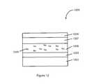
- FIGS. 1-8are simplified schematic diagrams illustrating a method and structure for forming a thin film photovoltaic device according to an embodiment of the present invention.
- FIGS. 9-12are simplified diagrams illustrating a method and structure for forming a thin film photovoltaic device including sodium species treatment according to an embodiment of the present invention.
- the present inventionprovides a method for manufacturing thin film photovoltaic devices.
- the methodhas been used to provide a copper indium disulfide thin film material for high efficiency solar cell application.
- the present inventionhas a much broader range of applicability, for example, embodiments of the present invention may be used to form other semiconducting thin films or multilayers comprising iron sulfide, cadmium sulfide, zinc selenide, and others, and metal oxides such as zinc oxide, iron oxide, copper oxide, and others.
- FIGS. 1-8are simplified schematic diagrams illustrating a method for forming a thin film photovoltaic device according to an embodiment of the present invention. These diagrams are merely examples, which should not unduly limit the claims herein. One skilled in the art would recognize other variations, modifications, and alternatives.
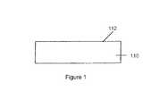
- a substrate 110is provided.
- the substrate 110includes a surface region 112 and is held in a process stage within a process chamber (not shown).
- the substrate 110is an optically transparent solid material.
- substrate 110can use material such as glass, quartz, fused silica, or plastic, or metal, or foil, or semiconductor, or composite materials.
- the substratecan be a single material, multiple materials, which are layered, composites, or stacked, including combinations of these, and the like. Of course there can be other variations, modifications, and alternatives.
- the present methodforms an electrode layer 120 overlying a surface region 112 of substrate 110 .
- the electrode layercan be a suitable metal material, a semiconductor material or a transparent conducting oxide material, or a combination.
- Electrode layer 120can be formed using techniques such as sputtering, evaporation (e.g., using electron beam), electro-plating, or a combination of these, and the like, according to a specific embodiment.
- the electrode layeris characterized by a resistivity of about 10 Ohm/cm 2 to 100 Ohm/cm 2 and less according to a specific embodiment.
- the electrode layercan be made of molybdenum or tungsten.
- the electrode layercan have a thickness ranging from about 100 nm to 2 micron in a specific embodiment, but can also be others depending on the application.
- Other suitable materialssuch as copper, chromium, aluminum, nickel, or platinum, and the like may also be used.
- copper, chromium, aluminum, nickel, or platinum, and the likemay also be used.
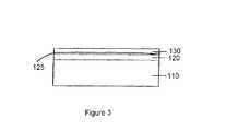
- a copper layer 130is formed overlying the electrode layer.
- copper (Cu) layer 130is formed overlying the electrode layer 120 .
- the copper layercan be formed using a sputtering process using a suitable copper target.
- a DC magnetron sputtering processcan be used to deposit Cu layer 130 onto the electrode layer 120 .
- the sputtering processis performed under a suitable pressure and temperature.
- the sputtering processcan be performed under a deposition pressure of about 6.2 mTorr.
- the deposition pressuremay be controlled using Ar gas.
- an Ar gas flow rate of about 32 sccmis used to achieve the desired deposition pressure.
- Depositioncan be provided at room temperature without heating the substrate. Of course, minor heating may result due to plasma generated during deposition. Additionally, a DC power supply of about 115 W may be used for the sputtering process. Depending on the embodiment, DC power ranging from 100 W to 150 W may be used depending on the specific materials used.
- a deposition time for a Cu layer of 330 nm thicknessis about 6 minutes or more under the described deposition condition. Of course, the deposition condition can be varied and modified according to a specific embodiment.
- the methodincludes forming a barrier layer 125 overlying the electrode layer to form an interface region between the electrode layer and the copper layer.
- the interface regionis maintained substantially free from a metal disulfide layer having a semiconductor characteristic that is different from a copper indium disulfide material formed during later processing steps.
- the barrier layerhas suitable conductive characteristics and can be reflective to allow electromagnetic radiation to reflect back into a photovoltaic cell or can also be transparent or the like.
- the barrier layeris selected from platinum, titanium, chromium, or silver. Of course, there can be other variations, modifications, and alternatives.
- the methodforms an indium layer 140 overlying copper layer 130 .
- the indium layeris deposited over the copper layer using a sputtering process in a specific embodiment.
- the indium layercan be deposited using a DC magnetron sputtering process under a similar condition for depositing the Cu layer.
- the deposition time for the indium layermay be shorter than that for Cu layer. As merely an example, 2 minutes and 45 seconds may be enough for depositing an In layer of about 410 nm in thickness according to a specific embodiment.
- the indium layercan be deposited overlying the copper layer using an electro-plating process, or others dependent on specific embodiment.
- FIGS. 1 through 4illustrate a method of forming a multilayered structure 150 comprising copper and indium on a substrate for a thin film photovoltaic device according to an embodiment of the present invention.
- copper layer 130 and indium layer 140are provided in a certain stoichiometry to allow for a Cu-rich material with an atomic ratio of Cu:In greater than 1 for the multilayered structure 150 .
- the atomic ratio Cu:Incan be in a range from about 1.2:1 to about 2.0:1 or larger depending upon the specific embodiment.
- the atomic ratio of Cu:Inis between 1.35:1 and 1.60:1.
- the atomic ratio of Cu:Inis selected to be about 1.55:1.
- the atomic ratio Cu:Inis provided such that Cu is limiting, which consumes essentially all of the indium species, in the resulting structure.
- indium layer 140is provided to cause substantially no change in the copper layer 130 formed until further processing.
- indium layer 140can be first deposited overlying the electrode layer followed by deposition of the copper layer 130 overlying the indium layer.
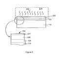
- multilayered structure 150is subjected to a thermal treatment process 200 .
- the thermal treatment processis provided in an environment containing at least a sulfur bearing species 210 .
- the thermal treatment processis performed at an adequate pressure and temperature.
- the thermal treatment processis provided at a temperature ranging from about 400 Degrees Celsius to about 600 Degrees Celsius.
- the thermal treatment processcan be a rapid thermal process provided at the temperature range for about three to fifteen minutes.
- the sulfur bearing speciesis in a fluid phase.
- the sulfur bearing speciescan be provided in a solution, which has dissolved Na 2 S, CS 2 , (NH 4 ) 2 S, thiosulfate, among others.
- the sulfur bearing species 210is gas phase hydrogen sulfide.
- the sulfur bearing speciescan be provided in a solid phase.
- elemental sulfurcan be heated and allowed to vaporize into a gas phase, e.g., as S n .
- the gas phase sulfuris allowed to react to the indium/copper layers.
- combinations of sulfur speciescan be used.
- the thermal treatment process 200includes certain predetermined ramp-up and ramp down time and ramp-up and ramp-down rate.
- the thermal treatment processis a rapid thermal annealing process.
- the hydrogen sulfide gasis provided through one or more entry valves with flow rate controls into the process chamber. The hydrogen sulfide gas pressure in the chamber may be controlled by one or more pumping systems or others, depending on the embodiment.
- the sulfur bearing speciescan be provided as a layer material overlying the indium and copper layers or copper and indium layers. In a specific embodiment, the sulfur bearing species is provided as a thin layer or as a patterned layer. Depending upon the embodiment, the sulfur bearing species can be provided as a slurry, a powder, a solid material, a gas, a paste, or other suitable form. Of course, there can be other variations, modifications, and alternatives.
- the thermal treatment process 200causes a reaction between copper indium material within the multilayered structure 150 and the sulfur bearing species 210 , thereby forming a layer of copper indium disulfide material (or a copper indium disulfide thin film) 220 .
- the copper indium disulfide material or copper indium disulfide thin film 220is formed by incorporating sulfur ions/atoms stripped or decomposed from the sulfur bearing species into the multilayered structure 150 with indium atoms and copper atoms mutually diffused therein.
- the thermal treatment process 200results in a formation of a cap layer 221 overlying the transformed copper indium disulfide material 220 .
- the cap layercontains a thickness of substantially copper sulfide material but substantially free of indium atoms.
- the cap layerincludes a surface region 225 .
- the formation of this cap layeris under a Cu-rich conditions for the Cu—In bearing multilayered structure 150 .
- the thickness of the copper sulfide material 221is on an order of about five to ten nanometers and greater based on original multilayered structure 150 with indium layer 140 overlying copper layer 130 .
- FIG. 6is a schematic diagram illustrating a process of the method for forming a thin film photovoltaic device according to an embodiment of the present invention.
- the diagramis merely an example, which should not unduly limit the claims herein.
- a dip process 300is performed to the copper sulfide material 221 that covers the copper indium disulfide thin film 220 .
- the dip processis performed by exposing the surface region 225 to a solution of potassium cyanide 310 in a specific embodiment.
- the solution of potassium cyanidehas a concentration of about 1 weight % to about 10 weight % according to a specific embodiment.
- the solution of potassium cyanideacts as an etchant that is capable of selectively removing copper sulfide material 221 from the surface region of the copper indium disulfide material.
- the etching processstarts from the exposed surface region 225 and down to the thickness of the copper sulfide material 221 and substantially stopped at the interface between the copper sulfide material 221 and copper indium disulfide material 220 .
- the copper sulfide cap layer 221is selectively removed by the etching process to expose surface region 228 of the copper indium disulfide thin film material according to a specific embodiment.
- the etch selectivityis about 1:100 or more between copper sulfide and copper indium disulfide material.
- etching speciescan be hydrogen peroxide.
- techniques including electro-chemical etching, plasma etching, sputter-etching, or any combination of thesemay be used.
- the copper sulfide materialcan be mechanically removed, chemically removed, electrically removed, or any combination of these, and others.
- an absorber layer made of copper indium disulfidecan have a thickness of about 1 to 10 microns, but can be others. Of course, there can be other variations, modifications, and alternatives.
- the methodfurther process the copper indium disulfide material to form a p-type copper indium disulfide film 320 in a specific embodiment.
- the as-formed copper indium disulfide materialmay have a desirable p-type semiconducting characteristic.
- copper indium disulfide material 220is subjected to a doping process to adjust p-type impurity concentration therein for the purpose of optimizing I-V characteristic of the high efficiency thin film photovoltaic devices.
- aluminum speciesare allowed to mix into the copper indium disulfide material 220 .
- the copper indium disulfide material 220is mixed with a copper indium aluminum disulfide material.
- a window layer 310is formed overlying the p-type copper indium disulfide material 320 .
- the window layercan be selected from a group consisting of a cadmium sulfide (CdS), a zinc sulfide (ZnS), zinc selenium (ZnSe), zinc oxide (ZnO), zinc magnesium oxide (ZnMgO), or others. In certain embodiments, these materials may be doped with one or more suitable impurities to form an n′ type semiconductor material.
- the window layer and the absorber layerforms a PN junction associated with a photovoltaic cell.
- the window layeris heavily doped to form a n + -type semiconductor layer in a preferred embodiment.
- indium speciesare used as the doping material to cause formation of the n + -type characteristic associated with the window layer 310 .
- the doping processis performed under suitable conditions.
- the window layercan use an aluminum doped ZnO material.
- the aluminum doped ZnO materialcan range from about 200 nm to about 500 nanometers in a specific embodiment.
- the methodforms a conductive layer 330 overlying a portion of a first surface region of the window layer 310 .
- the conductive layerforms a top electrode layer for the photovoltaic device.
- the conductive layer 330is a transparent conductive oxide (TCO).
- TCOtransparent conductive oxide
- the TCOcan be selected from a group consisting of In 2 O 3 :Sn (ITO), ZnO:Al (AZO), SnO 2 :F (TFO), and the like, but can be others.
- the TCO layeris provided in a certain predetermined pattern to maximize the fill factor and conversion efficiency of the photovoltaic device.
- the TCOcan also function as a window layer, which essentially eliminates a separate window layer.
- ITOIn 2 O 3 :Sn
- AZOZnO:Al
- TFOSnO 2 :F
- the TCO layeris provided in a certain predetermined pattern to maximize the fill factor and conversion efficiency of the photovoltaic device
- the present methodmaintains an interface region between the electrode layer and the copper indium disulfide material substantially free from a metal disulfide layer having different semiconductor characteristics from the copper indium disulfide material.
- the metal disulfide layeris selected from molybdenum disulfide layer or the like.
- the interface regionis characterized by a surface morphology substantially capable of preventing any formation of the metal disulfide layer, which is characterized by a thickness of about 5 nanometers to about 10 nanometers.
- the present methodincludes a thermal process during at least the maintaining process or a portion of the maintaining process of at least 300 Degrees Celsius and greater to prevent any formation of the metal disulfide layer, which can be a molybdenum disulfide or like layer.
- a thermal processduring at least the maintaining process or a portion of the maintaining process of at least 300 Degrees Celsius and greater to prevent any formation of the metal disulfide layer, which can be a molybdenum disulfide or like layer.
- the present inventionprovides a method for forming a thin film photovoltaic device, which is outlined below.
- a transparent substratecomprising a surface region
- the copper indium disulfide materialcomprising a copper-to-indium atomic ratio ranging from about 1.2:1 to about 2:1 or 1.35:1 to about 1.60:1 (or preferably and alternatively from about 0.99:1 or 0.95:1 and less) and a thickness of substantially copper sulfide material having a copper sulfide surface region;
- the present inventionprovides a method and resulting photovoltaic structure free from parasitic junction regions in the absorber layer, which impair performance of the resulting device.
- Other alternativescan also be provided where steps are added, one or more steps are removed, or one or more steps are provided in a different sequence without departing from the scope of the claims herein. Details of the present method and structure can be found throughout the present specification and more particularly below.
- FIGS. 9-11are simplified diagrams illustrating a method and structure for forming a thin film photovoltaic device including sodium species treatment according to an embodiment of the present invention. These diagrams are merely examples, which should not unduly limit the scope of the claims herein. One of ordinary skill in the art would recognize other variations, modifications, and alternatives.
- the present methodbegins with partially completed photovoltaic device 900 .
- the deviceincludes a transparent substrate 901 comprising a surface region, although other substrates can be used.
- the devicealso includes a first electrode layer 903 overlying the surface region.
- the first electrode layercan be any conductive material including conductive metals, oxides, and semiconductor or combinations of these, as well as any material described herein and outside of the present specification.
- the photovoltaic deviceincludes a chalcopyrite material, which acts as an absorber for the photovoltaic device.
- the chalcopyrite materialcan include, among others, copper indium disulfide material, copper indium aluminum disulfide, copper indium gallium disulfide, combinations of these, and others.
- the chalcopyriteis copper rich, or alternatively copper poor and characterized by one or more portions having a copper to indium atomic ratio of 0.99:1 and less or 0.95:1 and less.
- the copper indium disulfide materialhas one or more copper poor regions, which are preferably compensated using an ionic species.
- the chalcopyritehas a thin layer of copper sulfide 907 , which has been previously described, as may remain as a residue or fixed material when the bulk material is copper rich.
- copper sulfide 907which has been previously described, as may remain as a residue or fixed material when the bulk material is copper rich.
- the methodselectively removes the thin layer of copper sulfide.
- the thin layer of copper sulfideis removed 909 using a solution of potassium cyanide (KCN) or other suitable technique, e.g., dry etching, plasma etching, sputtering.
- KCNpotassium cyanide
- the methodmay cause formation of a copper poor surface region 1001 .
- the copper poor surfaceis characterized by a copper to indium atomic ratio of less than about 0.95:1 or 0.99:1.
- the copper poor surface regionis characterized as an n-type material, which forms a parasitic junction with the p-type copper indium disulfide material, which can be rich in copper.
- the parasitic junctionleads to poor or inefficient device performance.
- the present methodsubjects the copper poor surface to an ionic species to convert the copper poor surface from an n-type characteristic to a p-type characteristic, which behaves like a normal copper indium disulfide surface 1101 now, as shown in FIG. 11 .
- the methodsubjects at least one or more portions of the bulk copper indium disulfide material to one or more ionic species to convert the copper poor region from an n-type characteristic to a p-type characteristic.
- the ionic speciesis sodium, which can be derived from NaCl, Na 2 S, NaF, or other suitable sodium salts and the like.
- the subjecting the copper poor surface and/or bulk materialincludes a thermal treatment process during a time period associated with the subjecting of at least the copper poor surface with the ionic species.
- the thermal treatment processcan range in temperature from about 100 Degrees Celsius to about 500 Degrees Celsius, but can be others. Additionally, the thermal treatment process occurs for a time period ranging from a few minutes to about ten minutes to an hour or so.
- the thermal treatment processoccurs for a time period ranging from a few minutes to about ten minutes to an hour or so.
- the ionic speciescan be applied using one or more techniques. These techniques include deposition, sputtering, spin coating, spraying, spray pyrolysis, dipping, electro deposition, painting, ink jet coating, sprinkling, any combination of these, and others.
- the sodiumcan be diffused from an overlying material, which can be an electrode layer or molybdenum or other suitable material.
- sodiumcan be diffused from a piece of sodium material or the like via a vapor phase.
- the ionic species such as sodiumcan be diffused in vapor phase as in the “Siemens” process, but can be others, for short periods of time.
- the treatment processpassivates the surface at the heterojunction or the like, which facilitates carrier separation and transport. Additionally, the present treatment process can also generate desired conduction band offset, commonly called CBO. Of course, there can be other variations, modifications, and alternatives.
- the methodincludes forming a window layer overlying the copper indium disulfide material.
- the methodalso forms an electrode layer overlying the window layer.
- the photovoltaic cellcan be coupled to a glass or transparent plate or other suitable member.
- the photovoltaic cellcan be coupled to another cell, e.g., bottom cell, to form a tandem or multi junction cell. Again, there can be other variations, modifications, and alternatives.
- FIG. 12is a simplified diagram of an copper indium disulfide material having one or more copper poor regions according to an embodiment of the present invention.
- This diagramis merely an example, which should not unduly limit the scope of the claims herein.
- the diagramprovides a thin film photovoltaic device 1200 .
- the devicehas a substrate (e.g., transparent) 1201 comprising a surface region.
- the substratecan be made of any of the materials described herein as well as out side of the present specification.
- the devicehas a first electrode layer 1203 overlying the surface region and a chalcopyrite material 1205 , which is an absorber, overlying the surface region.
- the devicealso has a copper poor copper indium disulfide bulk region 1205 and a chalcopyrite material surface region.
- the copper poor copper indium disulfide bulk regionhaving an atomic ratio of Cu:In of about 0.99 and less.
- the devicehas compensating sodium species 1204 provided within one or more portions of the copper poor copper indium disulfide region to change the copper poor copper indium disulfide region from an n-type characteristic to a p-type characteristic.
- a window layer 1207overlying the copper indium disulfide region and a second electrode layer 1209 overlying the window layer.
- any of the elements described hereincan be made of any of the materials or combination of materials described within the present specification and outside of the specification as well.
Landscapes
- Engineering & Computer Science (AREA)
- Physics & Mathematics (AREA)
- Condensed Matter Physics & Semiconductors (AREA)
- General Physics & Mathematics (AREA)
- Manufacturing & Machinery (AREA)
- Computer Hardware Design (AREA)
- Microelectronics & Electronic Packaging (AREA)
- Power Engineering (AREA)
- Chemical & Material Sciences (AREA)
- Materials Engineering (AREA)
- Photovoltaic Devices (AREA)
Abstract
Description
Claims (26)
Priority Applications (2)
| Application Number | Priority Date | Filing Date | Title |
|---|---|---|---|
| US12/563,065US8008110B1 (en) | 2008-09-29 | 2009-09-18 | Bulk sodium species treatment of thin film photovoltaic cell and manufacturing method |
| US13/196,825US8258000B2 (en) | 2008-09-29 | 2011-08-02 | Bulk sodium species treatment of thin film photovoltaic cell and manufacturing method |
Applications Claiming Priority (2)
| Application Number | Priority Date | Filing Date | Title |
|---|---|---|---|
| US10086108P | 2008-09-29 | 2008-09-29 | |
| US12/563,065US8008110B1 (en) | 2008-09-29 | 2009-09-18 | Bulk sodium species treatment of thin film photovoltaic cell and manufacturing method |
Related Child Applications (1)
| Application Number | Title | Priority Date | Filing Date |
|---|---|---|---|
| US13/196,825ContinuationUS8258000B2 (en) | 2008-09-29 | 2011-08-02 | Bulk sodium species treatment of thin film photovoltaic cell and manufacturing method |
Publications (1)
| Publication Number | Publication Date |
|---|---|
| US8008110B1true US8008110B1 (en) | 2011-08-30 |
Family
ID=44486252
Family Applications (2)
| Application Number | Title | Priority Date | Filing Date |
|---|---|---|---|
| US12/563,065Expired - Fee RelatedUS8008110B1 (en) | 2008-09-29 | 2009-09-18 | Bulk sodium species treatment of thin film photovoltaic cell and manufacturing method |
| US13/196,825Expired - Fee RelatedUS8258000B2 (en) | 2008-09-29 | 2011-08-02 | Bulk sodium species treatment of thin film photovoltaic cell and manufacturing method |
Family Applications After (1)
| Application Number | Title | Priority Date | Filing Date |
|---|---|---|---|
| US13/196,825Expired - Fee RelatedUS8258000B2 (en) | 2008-09-29 | 2011-08-02 | Bulk sodium species treatment of thin film photovoltaic cell and manufacturing method |
Country Status (1)
| Country | Link |
|---|---|
| US (2) | US8008110B1 (en) |
Cited By (39)
| Publication number | Priority date | Publication date | Assignee | Title |
|---|---|---|---|---|
| US20110070688A1 (en)* | 2008-09-30 | 2011-03-24 | Stion Corporation | Thermal management and method for large scale processing of cis and/or cigs based thin films overlying glass substrates |
| US8193028B2 (en) | 2008-10-06 | 2012-06-05 | Stion Corporation | Sulfide species treatment of thin film photovoltaic cell and manufacturing method |
| US8198122B2 (en) | 2008-09-29 | 2012-06-12 | Stion Corporation | Bulk chloride species treatment of thin film photovoltaic cell and manufacturing method |
| US8236597B1 (en) | 2008-09-29 | 2012-08-07 | Stion Corporation | Bulk metal species treatment of thin film photovoltaic cell and manufacturing method |
| US8258000B2 (en)* | 2008-09-29 | 2012-09-04 | Stion Corporation | Bulk sodium species treatment of thin film photovoltaic cell and manufacturing method |
| US8263494B2 (en) | 2010-01-25 | 2012-09-11 | Stion Corporation | Method for improved patterning accuracy for thin film photovoltaic panels |
| US8287942B1 (en) | 2007-09-28 | 2012-10-16 | Stion Corporation | Method for manufacture of semiconductor bearing thin film material |
| US8314326B2 (en) | 2006-05-15 | 2012-11-20 | Stion Corporation | Method and structure for thin film photovoltaic materials using bulk semiconductor materials |
| US8344243B2 (en) | 2008-11-20 | 2013-01-01 | Stion Corporation | Method and structure for thin film photovoltaic cell using similar material junction |
| US8377736B2 (en) | 2008-10-02 | 2013-02-19 | Stion Corporation | System and method for transferring substrates in large scale processing of CIGS and/or CIS devices |
| US8383450B2 (en) | 2008-09-30 | 2013-02-26 | Stion Corporation | Large scale chemical bath system and method for cadmium sulfide processing of thin film photovoltaic materials |
| US8394662B1 (en) | 2008-09-29 | 2013-03-12 | Stion Corporation | Chloride species surface treatment of thin film photovoltaic cell and manufacturing method |
| US8398772B1 (en) | 2009-08-18 | 2013-03-19 | Stion Corporation | Method and structure for processing thin film PV cells with improved temperature uniformity |
| US8425739B1 (en) | 2008-09-30 | 2013-04-23 | Stion Corporation | In chamber sodium doping process and system for large scale cigs based thin film photovoltaic materials |
| US8435822B2 (en) | 2008-09-30 | 2013-05-07 | Stion Corporation | Patterning electrode materials free from berm structures for thin film photovoltaic cells |
| US8436445B2 (en) | 2011-08-15 | 2013-05-07 | Stion Corporation | Method of manufacture of sodium doped CIGS/CIGSS absorber layers for high efficiency photovoltaic devices |
| US8435826B1 (en) | 2008-10-06 | 2013-05-07 | Stion Corporation | Bulk sulfide species treatment of thin film photovoltaic cell and manufacturing method |
| US8461061B2 (en) | 2010-07-23 | 2013-06-11 | Stion Corporation | Quartz boat method and apparatus for thin film thermal treatment |
| US8476104B1 (en) | 2008-09-29 | 2013-07-02 | Stion Corporation | Sodium species surface treatment of thin film photovoltaic cell and manufacturing method |
| US8501521B1 (en) | 2008-09-29 | 2013-08-06 | Stion Corporation | Copper species surface treatment of thin film photovoltaic cell and manufacturing method |
| US8501507B2 (en) | 2007-11-14 | 2013-08-06 | Stion Corporation | Method for large scale manufacture of thin film photovoltaic devices using multi-chamber configuration |
| US8507786B1 (en) | 2009-06-27 | 2013-08-13 | Stion Corporation | Manufacturing method for patterning CIGS/CIS solar cells |
| US8557625B1 (en) | 2008-10-17 | 2013-10-15 | Stion Corporation | Zinc oxide film method and structure for cigs cell |
| US8617917B2 (en) | 2008-06-25 | 2013-12-31 | Stion Corporation | Consumable adhesive layer for thin film photovoltaic material |
| US8628997B2 (en) | 2010-10-01 | 2014-01-14 | Stion Corporation | Method and device for cadmium-free solar cells |
| US8642138B2 (en) | 2008-06-11 | 2014-02-04 | Stion Corporation | Processing method for cleaning sulfur entities of contact regions |
| US8673675B2 (en) | 2008-09-30 | 2014-03-18 | Stion Corporation | Humidity control and method for thin film photovoltaic materials |
| US8691618B2 (en) | 2008-09-29 | 2014-04-08 | Stion Corporation | Metal species surface treatment of thin film photovoltaic cell and manufacturing method |
| US8728200B1 (en) | 2011-01-14 | 2014-05-20 | Stion Corporation | Method and system for recycling processing gas for selenization of thin film photovoltaic materials |
| US8741689B2 (en) | 2008-10-01 | 2014-06-03 | Stion Corporation | Thermal pre-treatment process for soda lime glass substrate for thin film photovoltaic materials |
| US8759671B2 (en) | 2007-09-28 | 2014-06-24 | Stion Corporation | Thin film metal oxide bearing semiconductor material for single junction solar cell devices |
| US8809096B1 (en) | 2009-10-22 | 2014-08-19 | Stion Corporation | Bell jar extraction tool method and apparatus for thin film photovoltaic materials |
| US8859880B2 (en) | 2010-01-22 | 2014-10-14 | Stion Corporation | Method and structure for tiling industrial thin-film solar devices |
| US8871305B2 (en) | 2007-06-29 | 2014-10-28 | Stion Corporation | Methods for infusing one or more materials into nano-voids of nanoporous or nanostructured materials |
| US8941132B2 (en) | 2008-09-10 | 2015-01-27 | Stion Corporation | Application specific solar cell and method for manufacture using thin film photovoltaic materials |
| US8998606B2 (en) | 2011-01-14 | 2015-04-07 | Stion Corporation | Apparatus and method utilizing forced convection for uniform thermal treatment of thin film devices |
| US9087943B2 (en) | 2008-06-25 | 2015-07-21 | Stion Corporation | High efficiency photovoltaic cell and manufacturing method free of metal disulfide barrier material |
| US9096930B2 (en) | 2010-03-29 | 2015-08-04 | Stion Corporation | Apparatus for manufacturing thin film photovoltaic devices |
| CN106549070A (en)* | 2015-09-16 | 2017-03-29 | 株式会社东芝 | Photo-electric conversion element, solar cell, solar module and photovoltaic power generation system |
Families Citing this family (1)
| Publication number | Priority date | Publication date | Assignee | Title |
|---|---|---|---|---|
| US8586457B1 (en)* | 2012-05-17 | 2013-11-19 | Intermolecular, Inc. | Method of fabricating high efficiency CIGS solar cells |
Citations (35)
| Publication number | Priority date | Publication date | Assignee | Title |
|---|---|---|---|---|
| US4335266A (en) | 1980-12-31 | 1982-06-15 | The Boeing Company | Methods for forming thin-film heterojunction solar cells from I-III-VI.sub.2 |
| US4442310A (en) | 1982-07-15 | 1984-04-10 | Rca Corporation | Photodetector having enhanced back reflection |
| US4581108A (en) | 1984-01-06 | 1986-04-08 | Atlantic Richfield Company | Process of forming a compound semiconductive material |
| US4996108A (en) | 1989-01-17 | 1991-02-26 | Simon Fraser University | Sheets of transition metal dichalcogenides |
| US5125984A (en) | 1990-05-31 | 1992-06-30 | Siemens Aktiengesellschaft | Induced junction chalcopyrite solar cell |
| US5261968A (en) | 1992-01-13 | 1993-11-16 | Photon Energy, Inc. | Photovoltaic cell and method |
| US5501744A (en) | 1992-01-13 | 1996-03-26 | Photon Energy, Inc. | Photovoltaic cell having a p-type polycrystalline layer with large crystals |
| US5536333A (en) | 1992-05-12 | 1996-07-16 | Solar Cells, Inc. | Process for making photovoltaic devices and resultant product |
| US5665175A (en) | 1990-05-30 | 1997-09-09 | Safir; Yakov | Bifacial solar cell |
| US6307148B1 (en)* | 1999-03-29 | 2001-10-23 | Shinko Electric Industries Co., Ltd. | Compound semiconductor solar cell and production method thereof |
| US6328871B1 (en) | 1999-08-16 | 2001-12-11 | Applied Materials, Inc. | Barrier layer for electroplating processes |
| US6635307B2 (en) | 2001-12-12 | 2003-10-21 | Nanotek Instruments, Inc. | Manufacturing method for thin-film solar cells |
| US20050109392A1 (en) | 2002-09-30 | 2005-05-26 | Hollars Dennis R. | Manufacturing apparatus and method for large-scale production of thin-film solar cells |
| US20060220059A1 (en) | 2003-04-09 | 2006-10-05 | Matsushita Electric Industrial Co., Ltd | Solar cell |
| US7179677B2 (en) | 2003-09-03 | 2007-02-20 | Midwest Research Institute | ZnO/Cu(InGa)Se2 solar cells prepared by vapor phase Zn doping |
| US20070089782A1 (en) | 2003-10-02 | 2007-04-26 | Scheuten Glasgroep | Spherical or grain-shaped semiconductor element for use in solar cells and method for producing the same; method for producing a solar cell comprising said semiconductor element and solar cell |
| US20070116892A1 (en) | 2005-11-18 | 2007-05-24 | Daystar Technologies, Inc. | Methods and apparatus for treating a work piece with a vaporous element |
| US20070151596A1 (en) | 2004-02-20 | 2007-07-05 | Sharp Kabushiki Kaisha | Substrate for photoelectric conversion device, photoelectric conversion device, and stacked photoelectric conversion device |
| US20070169810A1 (en) | 2004-02-19 | 2007-07-26 | Nanosolar, Inc. | High-throughput printing of semiconductor precursor layer by use of chalcogen-containing vapor |
| US20080041446A1 (en) | 2006-08-09 | 2008-02-21 | Industrial Technology Research Institute | Dye-sensitized solar cells and method for fabricating same |
| US20080092945A1 (en) | 2006-10-24 | 2008-04-24 | Applied Quantum Technology Llc | Semiconductor Grain and Oxide Layer for Photovoltaic Cells |
| US20080092953A1 (en) | 2006-05-15 | 2008-04-24 | Stion Corporation | Method and structure for thin film photovoltaic materials using bulk semiconductor materials |
| US20090087942A1 (en) | 2005-08-05 | 2009-04-02 | Meyers Peter V | Manufacture of Photovoltaic Devices |
| US20090234987A1 (en) | 2008-03-12 | 2009-09-17 | Mips Technologies, Inc. | Efficient, Scalable and High Performance Mechanism for Handling IO Requests |
| US20090235987A1 (en) | 2008-03-24 | 2009-09-24 | Epv Solar, Inc. | Chemical Treatments to Enhance Photovoltaic Performance of CIGS |
| US20090235983A1 (en) | 2008-03-18 | 2009-09-24 | Applied Quantum Technology, Llc | Interlayer Design for Epitaxial Growth of Semiconductor Layers |
| US20090293945A1 (en) | 2008-06-02 | 2009-12-03 | Saint Gobain Glass France | Photovoltaic cell and photovoltaic cell substrate |
| US20100087016A1 (en) | 2008-04-15 | 2010-04-08 | Global Solar Energy, Inc. | Apparatus and methods for manufacturing thin-film solar cells |
| US20100087026A1 (en) | 2006-12-21 | 2010-04-08 | Helianthos B.V. | Method for making solar sub-cells from a solar cell |
| US20100096007A1 (en) | 2007-07-27 | 2010-04-22 | Saint-Gobain Glass France | Photovoltaic cell front face substrate and use of a substrate for a photovoltaic cell front face |
| US20100101649A1 (en) | 2006-11-14 | 2010-04-29 | Saint-Gobain Glass France | Porous layer, its manufacturing process and its applications |
| US20100101648A1 (en) | 2007-10-19 | 2010-04-29 | Sony Corporation | Dye-sensitized photoelectric conversion device and method of manufacturing the same |
| US20110070690A1 (en) | 2008-09-30 | 2011-03-24 | Stion Corporation | Thermal management and method for large scale processing of cis and/or cigs based thin films overlying glass substrates |
| US20110073181A1 (en) | 2008-09-30 | 2011-03-31 | Stion Corporation | Patterning electrode materials free from berm structures for thin film photovoltaic cells |
| US7960204B2 (en) | 2008-09-30 | 2011-06-14 | Stion Corporation | Method and structure for adhesion of absorber material for thin film photovoltaic cell |
Family Cites Families (166)
| Publication number | Priority date | Publication date | Assignee | Title |
|---|---|---|---|---|
| US3520732A (en) | 1965-10-22 | 1970-07-14 | Matsushita Electric Industrial Co Ltd | Photovoltaic cell and process of preparation of same |
| US3975211A (en) | 1975-03-28 | 1976-08-17 | Westinghouse Electric Corporation | Solar cells and method for making same |
| US4062038A (en) | 1976-01-28 | 1977-12-06 | International Business Machines Corporation | Radiation responsive device |
| US4332974A (en) | 1979-06-28 | 1982-06-01 | Chevron Research Company | Multilayer photovoltaic cell |
| US5217564A (en) | 1980-04-10 | 1993-06-08 | Massachusetts Institute Of Technology | Method of producing sheets of crystalline material and devices made therefrom |
| EP0191503A3 (en) | 1980-04-10 | 1986-09-10 | Massachusetts Institute Of Technology | Method of producing sheets of crystalline material |
| US4441113A (en) | 1981-02-13 | 1984-04-03 | Energy Conversion Devices, Inc. | P-Type semiconductor material having a wide band gap |
| US4465575A (en) | 1981-09-21 | 1984-08-14 | Atlantic Richfield Company | Method for forming photovoltaic cells employing multinary semiconductor films |
| DE3314197A1 (en) | 1982-04-28 | 1983-11-03 | Energy Conversion Devices, Inc., 48084 Troy, Mich. | P-CONDUCTING AMORPHOUS SILICON ALLOY WITH A LARGE BAND GAP AND MANUFACTURING PROCESS THEREFOR |
| US4518855A (en) | 1982-09-30 | 1985-05-21 | Spring-Mornne, Inc. | Method and apparatus for statically aligning shafts and monitoring shaft alignment |
| US4461922A (en) | 1983-02-14 | 1984-07-24 | Atlantic Richfield Company | Solar cell module |
| US4471155A (en) | 1983-04-15 | 1984-09-11 | Energy Conversion Devices, Inc. | Narrow band gap photovoltaic devices with enhanced open circuit voltage |
| US4724011A (en) | 1983-05-16 | 1988-02-09 | Atlantic Richfield Company | Solar cell interconnection by discrete conductive regions |
| US4517403A (en) | 1983-05-16 | 1985-05-14 | Atlantic Richfield Company | Series connected solar cells and method of formation |
| US4532372A (en) | 1983-12-23 | 1985-07-30 | Energy Conversion Devices, Inc. | Barrier layer for photovoltaic devices |
| US4598306A (en) | 1983-07-28 | 1986-07-01 | Energy Conversion Devices, Inc. | Barrier layer for photovoltaic devices |
| US4499658A (en) | 1983-09-06 | 1985-02-19 | Atlantic Richfield Company | Solar cell laminates |
| US4589194A (en) | 1983-12-29 | 1986-05-20 | Atlantic Richfield Company | Ultrasonic scribing of thin film solar cells |
| US4542255A (en) | 1984-01-03 | 1985-09-17 | Atlantic Richfield Company | Gridded thin film solar cell |
| US4661370A (en) | 1984-02-08 | 1987-04-28 | Atlantic Richfield Company | Electric discharge processing of thin films |
| US4507181A (en) | 1984-02-17 | 1985-03-26 | Energy Conversion Devices, Inc. | Method of electro-coating a semiconductor device |
| US4611091A (en) | 1984-12-06 | 1986-09-09 | Atlantic Richfield Company | CuInSe2 thin film solar cell with thin CdS and transparent window layer |
| US4599154A (en) | 1985-03-15 | 1986-07-08 | Atlantic Richfield Company | Electrically enhanced liquid jet processing |
| US4663495A (en) | 1985-06-04 | 1987-05-05 | Atlantic Richfield Company | Transparent photovoltaic module |
| US4638111A (en) | 1985-06-04 | 1987-01-20 | Atlantic Richfield Company | Thin film solar cell module |
| US4623601A (en) | 1985-06-04 | 1986-11-18 | Atlantic Richfield Company | Photoconductive device containing zinc oxide transparent conductive layer |
| JPH0682625B2 (en) | 1985-06-04 | 1994-10-19 | シーメンス ソーラー インダストリーズ,エル.ピー. | Deposition method of zinc oxide film |
| US4798660A (en) | 1985-07-16 | 1989-01-17 | Atlantic Richfield Company | Method for forming Cu In Se2 films |
| US4625070A (en) | 1985-08-30 | 1986-11-25 | Atlantic Richfield Company | Laminated thin film solar module |
| US4775425A (en) | 1987-07-27 | 1988-10-04 | Energy Conversion Devices, Inc. | P and n-type microcrystalline semiconductor alloy material including band gap widening elements, devices utilizing same |
| US4816082A (en) | 1987-08-19 | 1989-03-28 | Energy Conversion Devices, Inc. | Thin film solar cell including a spatially modulated intrinsic layer |
| US4968354A (en) | 1987-11-09 | 1990-11-06 | Fuji Electric Co., Ltd. | Thin film solar cell array |
| US5045409A (en) | 1987-11-27 | 1991-09-03 | Atlantic Richfield Company | Process for making thin film solar cell |
| US5008062A (en) | 1988-01-20 | 1991-04-16 | Siemens Solar Industries, L.P. | Method of fabricating photovoltaic module |
| US4915745A (en) | 1988-09-22 | 1990-04-10 | Atlantic Richfield Company | Thin film solar cell and method of making |
| US5180686A (en) | 1988-10-31 | 1993-01-19 | Energy Conversion Devices, Inc. | Method for continuously deposting a transparent oxide material by chemical pyrolysis |
| US4873118A (en) | 1988-11-18 | 1989-10-10 | Atlantic Richfield Company | Oxygen glow treating of ZnO electrode for thin film silicon solar cell |
| US4950615A (en) | 1989-02-06 | 1990-08-21 | International Solar Electric Technology, Inc. | Method and making group IIB metal - telluride films and solar cells |
| FR2646560B1 (en) | 1989-04-27 | 1994-01-14 | Solems Sa | METHOD FOR IMPROVING THE SPECTRAL RESPONSE OF AN IMPROVED PHOTOCONDUCTOR STRUCTURE, SOLAR CELL AND PHOTORECEPTIVE STRUCTURE |
| US5028274A (en) | 1989-06-07 | 1991-07-02 | International Solar Electric Technology, Inc. | Group I-III-VI2 semiconductor films for solar cell application |
| US5078803A (en) | 1989-09-22 | 1992-01-07 | Siemens Solar Industries L.P. | Solar cells incorporating transparent electrodes comprising hazy zinc oxide |
| JPH03124067A (en) | 1989-10-07 | 1991-05-27 | Showa Shell Sekiyu Kk | Photovoltaic device and its manufacture |
| US5011565A (en) | 1989-12-06 | 1991-04-30 | Mobil Solar Energy Corporation | Dotted contact solar cell and method of making same |
| US5154777A (en) | 1990-02-26 | 1992-10-13 | Mcdonnell Douglas Corporation | Advanced survivable space solar power system |
| DE59009771D1 (en) | 1990-07-24 | 1995-11-16 | Siemens Ag | Process for the manufacture of a chalcopyrite solar cell. |
| JP2729239B2 (en) | 1990-10-17 | 1998-03-18 | 昭和シェル石油株式会社 | Integrated photovoltaic device |
| US5528397A (en) | 1991-12-03 | 1996-06-18 | Kopin Corporation | Single crystal silicon transistors for display panels |
| US6784492B1 (en) | 1991-03-18 | 2004-08-31 | Canon Kabushiki Kaisha | Semiconductor device including a gate-insulated transistor |
| US5211824A (en) | 1991-10-31 | 1993-05-18 | Siemens Solar Industries L.P. | Method and apparatus for sputtering of a liquid |
| US5231047A (en) | 1991-12-19 | 1993-07-27 | Energy Conversion Devices, Inc. | High quality photovoltaic semiconductor material and laser ablation method of fabrication same |
| JPH05243596A (en) | 1992-03-02 | 1993-09-21 | Showa Shell Sekiyu Kk | Manufacture of laminated type solar cell |
| WO1993019491A1 (en) | 1992-03-19 | 1993-09-30 | Siemens Solar Gmbh | Weather-resistant thin layer solar module |
| US5298086A (en) | 1992-05-15 | 1994-03-29 | United Solar Systems Corporation | Method for the manufacture of improved efficiency tandem photovoltaic device and device manufactured thereby |
| EP0574716B1 (en) | 1992-05-19 | 1996-08-21 | Matsushita Electric Industrial Co., Ltd. | Method for preparing chalcopyrite-type compound |
| ATE170669T1 (en) | 1992-06-29 | 1998-09-15 | Canon Kk | RESIN COMPOSITION FOR SEALING AND A SEMICONDUCTOR DEVICE COVERED WITH SEALING RESIN COMPOSITION |
| EP0648373B1 (en) | 1992-06-29 | 2002-01-30 | United Solar Systems Corporation | Microwave energized deposition process with substrate temperature control |
| US5578503A (en) | 1992-09-22 | 1996-11-26 | Siemens Aktiengesellschaft | Rapid process for producing a chalcopyrite semiconductor on a substrate |
| US5474939A (en) | 1992-12-30 | 1995-12-12 | Siemens Solar Industries International | Method of making thin film heterojunction solar cell |
| DE4333407C1 (en) | 1993-09-30 | 1994-11-17 | Siemens Ag | Solar cell comprising a chalcopyrite absorber layer |
| US5738731A (en) | 1993-11-19 | 1998-04-14 | Mega Chips Corporation | Photovoltaic device |
| EP0658924B1 (en) | 1993-12-17 | 2000-07-12 | Canon Kabushiki Kaisha | Method of manufacturing electron-emitting device, electron source and image-forming apparatus |
| US5578103A (en) | 1994-08-17 | 1996-11-26 | Corning Incorporated | Alkali metal ion migration control |
| DE4442824C1 (en) | 1994-12-01 | 1996-01-25 | Siemens Ag | Solar cell having higher degree of activity |
| EP0729189A1 (en) | 1995-02-21 | 1996-08-28 | Interuniversitair Micro-Elektronica Centrum Vzw | Method of preparing solar cells and products obtained thereof |
| US5674325A (en) | 1995-06-07 | 1997-10-07 | Photon Energy, Inc. | Thin film photovoltaic device and process of manufacture |
| US6743723B2 (en) | 1995-09-14 | 2004-06-01 | Canon Kabushiki Kaisha | Method for fabricating semiconductor device |
| US5977476A (en) | 1996-10-16 | 1999-11-02 | United Solar Systems Corporation | High efficiency photovoltaic device |
| JP3249408B2 (en) | 1996-10-25 | 2002-01-21 | 昭和シェル石油株式会社 | Method and apparatus for manufacturing thin film light absorbing layer of thin film solar cell |
| JP3249407B2 (en) | 1996-10-25 | 2002-01-21 | 昭和シェル石油株式会社 | Thin-film solar cells composed of chalcopyrite-based multi-compound semiconductor thin-film light-absorbing layers |
| JP3527815B2 (en) | 1996-11-08 | 2004-05-17 | 昭和シェル石油株式会社 | Method for producing transparent conductive film of thin film solar cell |
| US5985691A (en) | 1997-05-16 | 1999-11-16 | International Solar Electric Technology, Inc. | Method of making compound semiconductor films and making related electronic devices |
| JPH1154773A (en) | 1997-08-01 | 1999-02-26 | Canon Inc | Photovoltaic element and method for manufacturing the same |
| DE19741832A1 (en) | 1997-09-23 | 1999-03-25 | Inst Solarenergieforschung | Method of manufacturing a solar cell and solar cell |
| US6258620B1 (en) | 1997-10-15 | 2001-07-10 | University Of South Florida | Method of manufacturing CIGS photovoltaic devices |
| JP2001523049A (en) | 1997-11-10 | 2001-11-20 | スターメガ コーポレイション | Quantum ridges and quantum peaks |
| DE69911529T2 (en) | 1998-02-05 | 2004-08-05 | Nippon Sheet Glass Co., Ltd. | OBJECT WITH A LEVEL SURFACE, METHOD FOR THE PRODUCTION THEREOF AND COMPILATION THEREFOR |
| US6107562A (en) | 1998-03-24 | 2000-08-22 | Matsushita Electric Industrial Co., Ltd. | Semiconductor thin film, method for manufacturing the same, and solar cell using the same |
| US6344608B2 (en) | 1998-06-30 | 2002-02-05 | Canon Kabushiki Kaisha | Photovoltaic element |
| US6127202A (en) | 1998-07-02 | 2000-10-03 | International Solar Electronic Technology, Inc. | Oxide-based method of making compound semiconductor films and making related electronic devices |
| JP3428931B2 (en) | 1998-09-09 | 2003-07-22 | キヤノン株式会社 | Flat panel display dismantling method |
| JP2000150861A (en) | 1998-11-16 | 2000-05-30 | Tdk Corp | Oxide thin film |
| JP3667178B2 (en) | 1998-11-24 | 2005-07-06 | キヤノン株式会社 | Method for producing zinc oxide thin film, method for producing photovoltaic element using the same, and photovoltaic element |
| JP2000173969A (en) | 1998-12-03 | 2000-06-23 | Canon Inc | Rinse method and photovoltaic device |
| JP2001156321A (en) | 1999-03-09 | 2001-06-08 | Fuji Xerox Co Ltd | Semiconductor device and method of manufacturing the same |
| WO2001057932A1 (en) | 2000-02-07 | 2001-08-09 | Cis Solartechnik Gmbh | Flexible metal substrate for cis solar cells, and method for producing the same |
| US7194197B1 (en) | 2000-03-16 | 2007-03-20 | Global Solar Energy, Inc. | Nozzle-based, vapor-phase, plume delivery structure for use in production of thin-film deposition layer |
| US6372538B1 (en) | 2000-03-16 | 2002-04-16 | University Of Delaware | Fabrication of thin-film, flexible photovoltaic module |
| US6423565B1 (en) | 2000-05-30 | 2002-07-23 | Kurt L. Barth | Apparatus and processes for the massproduction of photovotaic modules |
| US7301199B2 (en) | 2000-08-22 | 2007-11-27 | President And Fellows Of Harvard College | Nanoscale wires and related devices |
| CN101798057A (en) | 2000-08-22 | 2010-08-11 | 哈佛学院董事会 | Doped elongated semiconductors, growing such semiconductors, devices including such semiconductors and fabricating such devices |
| JP2002196337A (en) | 2000-09-06 | 2002-07-12 | Seiko Epson Corp | Method and apparatus for manufacturing electro-optical device, and method and apparatus for manufacturing liquid crystal panel |
| US6576112B2 (en) | 2000-09-19 | 2003-06-10 | Canon Kabushiki Kaisha | Method of forming zinc oxide film and process for producing photovoltaic device using it |
| JP2002167695A (en) | 2000-09-19 | 2002-06-11 | Canon Inc | Method for forming zinc oxide film and method for manufacturing photovoltaic element using the same |
| DE10104726A1 (en) | 2001-02-02 | 2002-08-08 | Siemens Solar Gmbh | Process for structuring an oxide layer applied to a carrier material |
| JP4827303B2 (en) | 2001-03-12 | 2011-11-30 | キヤノン株式会社 | Photovoltaic element, TFT, and method for forming i-type semiconductor layer |
| US6858308B2 (en) | 2001-03-12 | 2005-02-22 | Canon Kabushiki Kaisha | Semiconductor element, and method of forming silicon-based film |
| JP2002299670A (en) | 2001-04-03 | 2002-10-11 | Canon Inc | Silicon based thin film and photovoltaic device |
| US7842882B2 (en) | 2004-03-01 | 2010-11-30 | Basol Bulent M | Low cost and high throughput deposition methods and apparatus for high density semiconductor film growth |
| US7053294B2 (en) | 2001-07-13 | 2006-05-30 | Midwest Research Institute | Thin-film solar cell fabricated on a flexible metallic substrate |
| JP4236081B2 (en) | 2001-10-16 | 2009-03-11 | 大日本印刷株式会社 | Method for producing pattern forming body |
| EP1443527A4 (en) | 2001-10-19 | 2007-09-12 | Asahi Glass Co Ltd | TRANSPARENT CONDUCTIVE OXIDE LAYER SUBSTRATE, PROCESS FOR PRODUCING THE SAME, AND PHOTOELECTRIC CONVERSION ELEMENT |
| US7276749B2 (en) | 2002-02-05 | 2007-10-02 | E-Phocus, Inc. | Image sensor with microcrystalline germanium photodiode layer |
| US6690041B2 (en) | 2002-05-14 | 2004-02-10 | Global Solar Energy, Inc. | Monolithically integrated diodes in thin-film photovoltaic devices |
| US7291782B2 (en) | 2002-06-22 | 2007-11-06 | Nanosolar, Inc. | Optoelectronic device and fabrication method |
| US6852920B2 (en) | 2002-06-22 | 2005-02-08 | Nanosolar, Inc. | Nano-architected/assembled solar electricity cell |
| TW200425530A (en) | 2002-09-05 | 2004-11-16 | Nanosys Inc | Nanostructure and nanocomposite based compositions and photovoltaic devices |
| WO2004022637A2 (en) | 2002-09-05 | 2004-03-18 | Nanosys, Inc. | Nanocomposites |
| US6849798B2 (en) | 2002-12-17 | 2005-02-01 | General Electric Company | Photovoltaic cell using stable Cu2O nanocrystals and conductive polymers |
| US6936761B2 (en) | 2003-03-29 | 2005-08-30 | Nanosolar, Inc. | Transparent electrode, optoelectronic apparatus and devices |
| US7279832B2 (en) | 2003-04-01 | 2007-10-09 | Innovalight, Inc. | Phosphor materials and illumination devices made therefrom |
| US20040252488A1 (en) | 2003-04-01 | 2004-12-16 | Innovalight | Light-emitting ceiling tile |
| JP2004332043A (en) | 2003-05-07 | 2004-11-25 | Canon Inc | Method and apparatus for forming zinc oxide thin film, and method for forming photovoltaic element |
| US7462774B2 (en) | 2003-05-21 | 2008-12-09 | Nanosolar, Inc. | Photovoltaic devices fabricated from insulating nanostructured template |
| US7265037B2 (en) | 2003-06-20 | 2007-09-04 | The Regents Of The University Of California | Nanowire array and nanowire solar cells and methods for forming the same |
| KR100838805B1 (en) | 2003-07-14 | 2008-06-17 | 가부시키가이샤후지쿠라 | Electrolyte composition, photoelectric conversion element and dye-sensitized solar cell using same |
| US20070163643A1 (en) | 2004-02-19 | 2007-07-19 | Nanosolar, Inc. | High-throughput printing of chalcogen layer and the use of an inter-metallic material |
| US8623448B2 (en) | 2004-02-19 | 2014-01-07 | Nanosolar, Inc. | High-throughput printing of semiconductor precursor layer from chalcogenide microflake particles |
| US7441413B2 (en)* | 2004-03-23 | 2008-10-28 | Samsung Electronics Co., Ltd. | Refrigerator and control method thereof |
| JP2005311292A (en) | 2004-03-25 | 2005-11-04 | Kaneka Corp | Substrate for thin film solar cell, manufacturing method therefor, and thin film solar cell using the same |
| US7122398B1 (en) | 2004-03-25 | 2006-10-17 | Nanosolar, Inc. | Manufacturing of optoelectronic devices |
| JP4695850B2 (en) | 2004-04-28 | 2011-06-08 | 本田技研工業株式会社 | Chalcopyrite solar cell |
| EP1797584A4 (en) | 2004-06-08 | 2014-08-13 | Sandisk Corp | METHODS AND DEVICES FOR FORMING NANOSTRUCTURE MONOLAYERS AND DEVICES COMPRISING SUCH SINGLES |
| TWI406890B (en) | 2004-06-08 | 2013-09-01 | Sandisk Corp | Post-deposition encapsulation of nanostructures : compositions, devices and systems incorporating same |
| DE112005001429T5 (en) | 2004-06-18 | 2007-04-26 | Innovalight, Inc., St. Paul | Method and apparatus for forming nanoparticles using radio frequency plasmas |
| US7442320B2 (en) | 2004-06-18 | 2008-10-28 | Ultradots, Inc. | Nanostructured materials and photovoltaic devices including nanostructured materials |
| JP2006049768A (en) | 2004-08-09 | 2006-02-16 | Showa Shell Sekiyu Kk | CIS-based compound semiconductor thin film solar cell and method for producing light absorption layer of solar cell |
| US7750352B2 (en) | 2004-08-10 | 2010-07-06 | Pinion Technologies, Inc. | Light strips for lighting and backlighting applications |
| US7732229B2 (en) | 2004-09-18 | 2010-06-08 | Nanosolar, Inc. | Formation of solar cells with conductive barrier layers and foil substrates |
| US7276724B2 (en) | 2005-01-20 | 2007-10-02 | Nanosolar, Inc. | Series interconnected optoelectronic device module assembly |
| US20060249202A1 (en) | 2004-09-20 | 2006-11-09 | Seunghyup Yoo | Photovoltaic cell |
| US20060096536A1 (en) | 2004-11-10 | 2006-05-11 | Daystar Technologies, Inc. | Pressure control system in a photovoltaic substrate deposition apparatus |
| CA2586970A1 (en) | 2004-11-10 | 2006-05-18 | Daystar Technologies, Inc. | Vertical production of photovoltaic devices |
| WO2006053032A1 (en) | 2004-11-10 | 2006-05-18 | Daystar Technologies, Inc. | Thermal process for creation of an in-situ junction layer in cigs |
| US20060219288A1 (en) | 2004-11-10 | 2006-10-05 | Daystar Technologies, Inc. | Process and photovoltaic device using an akali-containing layer |
| CN101233260A (en) | 2004-11-10 | 2008-07-30 | 德斯塔尔科技公司 | Pressure control system in photovoltaic substrate deposition |
| US20060130890A1 (en) | 2004-12-20 | 2006-06-22 | Palo Alto Research Center Incorporated. | Heterojunction photovoltaic cell |
| JP2006179626A (en) | 2004-12-22 | 2006-07-06 | Showa Shell Sekiyu Kk | CIS-based thin-film solar cell module, method for producing the solar cell module, and separation method |
| JP2006186200A (en) | 2004-12-28 | 2006-07-13 | Showa Shell Sekiyu Kk | Precursor film and film forming method thereof |
| JP2006183117A (en) | 2004-12-28 | 2006-07-13 | Showa Shell Sekiyu Kk | Manufacturing method of ZnO-based transparent conductive film by MOCVD (metal organic chemical vapor deposition) |
| JP4131965B2 (en) | 2004-12-28 | 2008-08-13 | 昭和シェル石油株式会社 | Method for producing light absorption layer of CIS thin film solar cell |
| KR100495925B1 (en) | 2005-01-12 | 2005-06-17 | (주)인솔라텍 | Optical absorber layers for solar cell and manufacturing method thereof |
| JP4801928B2 (en) | 2005-04-25 | 2011-10-26 | 富士フイルム株式会社 | Organic electroluminescence device |
| JP4841173B2 (en) | 2005-05-27 | 2011-12-21 | 昭和シェル石油株式会社 | High resistance buffer layer / window layer continuous film forming method and film forming apparatus for CIS thin film solar cell |
| JP3963924B2 (en) | 2005-07-22 | 2007-08-22 | 本田技研工業株式会社 | Chalcopyrite solar cell |
| JP2007123721A (en) | 2005-10-31 | 2007-05-17 | Rohm Co Ltd | Method for manufacturing photoelectric conversion device and photoelectric conversion device |
| DE102005062977B3 (en) | 2005-12-28 | 2007-09-13 | Sulfurcell Solartechnik Gmbh | Method and apparatus for converting metallic precursor layers to chalcopyrite layers of CIGSS solar cells |
| US8389852B2 (en) | 2006-02-22 | 2013-03-05 | Guardian Industries Corp. | Electrode structure for use in electronic device and method of making same |
| US7235736B1 (en) | 2006-03-18 | 2007-06-26 | Solyndra, Inc. | Monolithic integration of cylindrical solar cells |
| US9105776B2 (en) | 2006-05-15 | 2015-08-11 | Stion Corporation | Method and structure for thin film photovoltaic materials using semiconductor materials |
| US8617640B2 (en) | 2006-06-12 | 2013-12-31 | Nanosolar, Inc. | Thin-film devices formed from solid group IIIA alloy particles |
| DE102006041046A1 (en) | 2006-09-01 | 2008-03-06 | Cis Solartechnik Gmbh & Co. Kg | Solar cell, process for the production of solar cells and electrical trace |
| US8203073B2 (en) | 2006-11-02 | 2012-06-19 | Guardian Industries Corp. | Front electrode for use in photovoltaic device and method of making same |
| US20080121264A1 (en) | 2006-11-28 | 2008-05-29 | Industrial Technology Research Institute | Thin film solar module and method of fabricating the same |
| WO2008095146A2 (en) | 2007-01-31 | 2008-08-07 | Van Duren Jeroen K J | Solar cell absorber layer formed from metal ion precursors |
| KR100882668B1 (en) | 2007-07-18 | 2009-02-06 | 삼성모바일디스플레이주식회사 | Organic light emitting display device and manufacturing method thereof |
| US7998762B1 (en) | 2007-11-14 | 2011-08-16 | Stion Corporation | Method and system for large scale manufacture of thin film photovoltaic devices using multi-chamber configuration |
| JP2009135337A (en) | 2007-11-30 | 2009-06-18 | Showa Shell Sekiyu Kk | Laminated structure of CIS solar cell, integrated structure of CIS thin film solar cell, and manufacturing method |
| JP4384237B2 (en) | 2008-05-19 | 2009-12-16 | 昭和シェル石油株式会社 | CIS type thin film solar cell manufacturing method |
| US7855089B2 (en) | 2008-09-10 | 2010-12-21 | Stion Corporation | Application specific solar cell and method for manufacture using thin film photovoltaic materials |
| US8008110B1 (en)* | 2008-09-29 | 2011-08-30 | Stion Corporation | Bulk sodium species treatment of thin film photovoltaic cell and manufacturing method |
| US8008112B1 (en) | 2008-09-29 | 2011-08-30 | Stion Corporation | Bulk chloride species treatment of thin film photovoltaic cell and manufacturing method |
| US8008111B1 (en) | 2008-09-29 | 2011-08-30 | Stion Corporation | Bulk copper species treatment of thin film photovoltaic cell and manufacturing method |
| US8026122B1 (en) | 2008-09-29 | 2011-09-27 | Stion Corporation | Metal species surface treatment of thin film photovoltaic cell and manufacturing method |
| US8003430B1 (en) | 2008-10-06 | 2011-08-23 | Stion Corporation | Sulfide species treatment of thin film photovoltaic cell and manufacturing method |
| US8344243B2 (en) | 2008-11-20 | 2013-01-01 | Stion Corporation | Method and structure for thin film photovoltaic cell using similar material junction |
| US20100197051A1 (en) | 2009-02-04 | 2010-08-05 | Applied Materials, Inc. | Metrology and inspection suite for a solar production line |
- 2009
- 2009-09-18USUS12/563,065patent/US8008110B1/ennot_activeExpired - Fee Related
- 2011
- 2011-08-02USUS13/196,825patent/US8258000B2/ennot_activeExpired - Fee Related
Patent Citations (39)
| Publication number | Priority date | Publication date | Assignee | Title |
|---|---|---|---|---|
| US4335266A (en) | 1980-12-31 | 1982-06-15 | The Boeing Company | Methods for forming thin-film heterojunction solar cells from I-III-VI.sub.2 |
| US4442310A (en) | 1982-07-15 | 1984-04-10 | Rca Corporation | Photodetector having enhanced back reflection |
| US4581108A (en) | 1984-01-06 | 1986-04-08 | Atlantic Richfield Company | Process of forming a compound semiconductive material |
| US4996108A (en) | 1989-01-17 | 1991-02-26 | Simon Fraser University | Sheets of transition metal dichalcogenides |
| US5665175A (en) | 1990-05-30 | 1997-09-09 | Safir; Yakov | Bifacial solar cell |
| US5125984A (en) | 1990-05-31 | 1992-06-30 | Siemens Aktiengesellschaft | Induced junction chalcopyrite solar cell |
| US5501744A (en) | 1992-01-13 | 1996-03-26 | Photon Energy, Inc. | Photovoltaic cell having a p-type polycrystalline layer with large crystals |
| US5261968A (en) | 1992-01-13 | 1993-11-16 | Photon Energy, Inc. | Photovoltaic cell and method |
| US5536333A (en) | 1992-05-12 | 1996-07-16 | Solar Cells, Inc. | Process for making photovoltaic devices and resultant product |
| US6307148B1 (en)* | 1999-03-29 | 2001-10-23 | Shinko Electric Industries Co., Ltd. | Compound semiconductor solar cell and production method thereof |
| US6328871B1 (en) | 1999-08-16 | 2001-12-11 | Applied Materials, Inc. | Barrier layer for electroplating processes |
| US6635307B2 (en) | 2001-12-12 | 2003-10-21 | Nanotek Instruments, Inc. | Manufacturing method for thin-film solar cells |
| US20050109392A1 (en) | 2002-09-30 | 2005-05-26 | Hollars Dennis R. | Manufacturing apparatus and method for large-scale production of thin-film solar cells |
| US20090145746A1 (en) | 2002-09-30 | 2009-06-11 | Miasole | Manufacturing apparatus and method for large-scale production of thin-film solar cells |
| US7544884B2 (en) | 2002-09-30 | 2009-06-09 | Miasole | Manufacturing method for large-scale production of thin-film solar cells |
| US20060220059A1 (en) | 2003-04-09 | 2006-10-05 | Matsushita Electric Industrial Co., Ltd | Solar cell |
| US7179677B2 (en) | 2003-09-03 | 2007-02-20 | Midwest Research Institute | ZnO/Cu(InGa)Se2 solar cells prepared by vapor phase Zn doping |
| US20070089782A1 (en) | 2003-10-02 | 2007-04-26 | Scheuten Glasgroep | Spherical or grain-shaped semiconductor element for use in solar cells and method for producing the same; method for producing a solar cell comprising said semiconductor element and solar cell |
| US20070169810A1 (en) | 2004-02-19 | 2007-07-26 | Nanosolar, Inc. | High-throughput printing of semiconductor precursor layer by use of chalcogen-containing vapor |
| US20070151596A1 (en) | 2004-02-20 | 2007-07-05 | Sharp Kabushiki Kaisha | Substrate for photoelectric conversion device, photoelectric conversion device, and stacked photoelectric conversion device |
| US20090087942A1 (en) | 2005-08-05 | 2009-04-02 | Meyers Peter V | Manufacture of Photovoltaic Devices |
| US7442413B2 (en) | 2005-11-18 | 2008-10-28 | Daystar Technologies, Inc. | Methods and apparatus for treating a work piece with a vaporous element |
| US20070116892A1 (en) | 2005-11-18 | 2007-05-24 | Daystar Technologies, Inc. | Methods and apparatus for treating a work piece with a vaporous element |
| US20080092953A1 (en) | 2006-05-15 | 2008-04-24 | Stion Corporation | Method and structure for thin film photovoltaic materials using bulk semiconductor materials |
| US20080041446A1 (en) | 2006-08-09 | 2008-02-21 | Industrial Technology Research Institute | Dye-sensitized solar cells and method for fabricating same |
| US20080092945A1 (en) | 2006-10-24 | 2008-04-24 | Applied Quantum Technology Llc | Semiconductor Grain and Oxide Layer for Photovoltaic Cells |
| US20100101649A1 (en) | 2006-11-14 | 2010-04-29 | Saint-Gobain Glass France | Porous layer, its manufacturing process and its applications |
| US20100087026A1 (en) | 2006-12-21 | 2010-04-08 | Helianthos B.V. | Method for making solar sub-cells from a solar cell |
| US20100096007A1 (en) | 2007-07-27 | 2010-04-22 | Saint-Gobain Glass France | Photovoltaic cell front face substrate and use of a substrate for a photovoltaic cell front face |
| US20100101648A1 (en) | 2007-10-19 | 2010-04-29 | Sony Corporation | Dye-sensitized photoelectric conversion device and method of manufacturing the same |
| US20090234987A1 (en) | 2008-03-12 | 2009-09-17 | Mips Technologies, Inc. | Efficient, Scalable and High Performance Mechanism for Handling IO Requests |
| US20090235983A1 (en) | 2008-03-18 | 2009-09-24 | Applied Quantum Technology, Llc | Interlayer Design for Epitaxial Growth of Semiconductor Layers |
| US20090235987A1 (en) | 2008-03-24 | 2009-09-24 | Epv Solar, Inc. | Chemical Treatments to Enhance Photovoltaic Performance of CIGS |
| US20100087016A1 (en) | 2008-04-15 | 2010-04-08 | Global Solar Energy, Inc. | Apparatus and methods for manufacturing thin-film solar cells |
| US20090293945A1 (en) | 2008-06-02 | 2009-12-03 | Saint Gobain Glass France | Photovoltaic cell and photovoltaic cell substrate |
| US20110070690A1 (en) | 2008-09-30 | 2011-03-24 | Stion Corporation | Thermal management and method for large scale processing of cis and/or cigs based thin films overlying glass substrates |
| US20110073181A1 (en) | 2008-09-30 | 2011-03-31 | Stion Corporation | Patterning electrode materials free from berm structures for thin film photovoltaic cells |
| US7955891B2 (en) | 2008-09-30 | 2011-06-07 | Stion Corporation | Thermal management and method for large scale processing of CIS and /or CIGS based thin films overlying glass substrates |
| US7960204B2 (en) | 2008-09-30 | 2011-06-14 | Stion Corporation | Method and structure for adhesion of absorber material for thin film photovoltaic cell |
Non-Patent Citations (19)
| Title |
|---|
| Ellmer et al., Copper Indium Disulfide Solar Cell Absorbers Prepared in a One-Step Process by Reactive Magnetron Sputtering from Copper and Indium Targets; Elsevier Science B.V; Thin Solid Films 413 (2002) pp. 92-97. |
| Final Office Action of May 31, 2011for U.S. Appl. No. 12/621,489, 13 pages. |
| International Search Report & Written Opinion of PCT Application No. PCT/US 09/46161, date of mailing Jul. 27, 2009, 14 pages total. |
| International Search Report & Written Opinion of PCT Application No. PCT/US 09/46802, mailed on Jul. 31, 2009, 11 pages total. |
| Non-Final Office Action of Apr. 28, 2011 for U.S. Appl. No. 12/237,369, 17 pages. |
| Non-Final Office Action of May 2, 2011 for U.S. Appl. No. 12/953,701, 9 pages. |
| Non-Final Office Action of May 2, 2011 for U.S. Appl. No. 12/953,708, 9 pages. |
| Non-Final Office Action of May 2, 2011 for U.S. Appl. No. 12/953,716, 9 pages. |
| Non-Final Office Action of May 2, 2011 for U.S. Appl. No. 12/953,721, 9 pages. |
| Non-Final Office Action of May 2, 2011 for U.S. Appl. No. 12/953,725, 9 pages. |
| Non-Final Office Action of May 2, 2011 for U.S. Appl. No. 12/953,729, 9 pages. |
| Notice of Allowance of Apr. 19, 2011 for U.S. Appl. No. 12/567,715, 11 pages. |
| Notice of Allowance of Apr. 26, 2011 for U.S. Appl. No. 12/564,046, 11 pages. |
| Notice of Allowance of Apr. 27, 2011 for U.S. Appl. No. 12/564,886, 11 pages. |
| Notice of Allowance of Apr. 5, 2011 for U.S. Appl. No. 12/953,674, 11 pages. |
| Notice of Allowance of Apr. 5, 2011 for U.S. Appl. No. 12/953,679, 11 pages. |
| Notice of Allowance of Apr. 8, 2011 for U.S. Appl. No. 12/953,697, 11 pages. |
| Notice of Allowance of May 25, 2011 for U.S. Appl. No. 12/566,651, 8 pages. |
| Onuma et al., Preparation and Characterization of CuInS Thin Films Solar Cells with Large Grain, Elsevier Science B.V; Solar Energy Materials & Solar Cells 69 (2001) pp. 261-269. |
Cited By (50)
| Publication number | Priority date | Publication date | Assignee | Title |
|---|---|---|---|---|
| US8314326B2 (en) | 2006-05-15 | 2012-11-20 | Stion Corporation | Method and structure for thin film photovoltaic materials using bulk semiconductor materials |
| US8871305B2 (en) | 2007-06-29 | 2014-10-28 | Stion Corporation | Methods for infusing one or more materials into nano-voids of nanoporous or nanostructured materials |
| US8287942B1 (en) | 2007-09-28 | 2012-10-16 | Stion Corporation | Method for manufacture of semiconductor bearing thin film material |
| US8759671B2 (en) | 2007-09-28 | 2014-06-24 | Stion Corporation | Thin film metal oxide bearing semiconductor material for single junction solar cell devices |
| US8642361B2 (en) | 2007-11-14 | 2014-02-04 | Stion Corporation | Method and system for large scale manufacture of thin film photovoltaic devices using multi-chamber configuration |
| US8623677B2 (en) | 2007-11-14 | 2014-01-07 | Stion Corporation | Method and system for large scale manufacture of thin film photovoltaic devices using multi-chamber configuration |
| US8512528B2 (en) | 2007-11-14 | 2013-08-20 | Stion Corporation | Method and system for large scale manufacture of thin film photovoltaic devices using single-chamber configuration |
| US8501507B2 (en) | 2007-11-14 | 2013-08-06 | Stion Corporation | Method for large scale manufacture of thin film photovoltaic devices using multi-chamber configuration |
| US8642138B2 (en) | 2008-06-11 | 2014-02-04 | Stion Corporation | Processing method for cleaning sulfur entities of contact regions |
| US9087943B2 (en) | 2008-06-25 | 2015-07-21 | Stion Corporation | High efficiency photovoltaic cell and manufacturing method free of metal disulfide barrier material |
| US8617917B2 (en) | 2008-06-25 | 2013-12-31 | Stion Corporation | Consumable adhesive layer for thin film photovoltaic material |
| US8941132B2 (en) | 2008-09-10 | 2015-01-27 | Stion Corporation | Application specific solar cell and method for manufacture using thin film photovoltaic materials |
| US8691618B2 (en) | 2008-09-29 | 2014-04-08 | Stion Corporation | Metal species surface treatment of thin film photovoltaic cell and manufacturing method |
| US8476104B1 (en) | 2008-09-29 | 2013-07-02 | Stion Corporation | Sodium species surface treatment of thin film photovoltaic cell and manufacturing method |
| US8198122B2 (en) | 2008-09-29 | 2012-06-12 | Stion Corporation | Bulk chloride species treatment of thin film photovoltaic cell and manufacturing method |
| US8236597B1 (en) | 2008-09-29 | 2012-08-07 | Stion Corporation | Bulk metal species treatment of thin film photovoltaic cell and manufacturing method |
| US8258000B2 (en)* | 2008-09-29 | 2012-09-04 | Stion Corporation | Bulk sodium species treatment of thin film photovoltaic cell and manufacturing method |
| US8501521B1 (en) | 2008-09-29 | 2013-08-06 | Stion Corporation | Copper species surface treatment of thin film photovoltaic cell and manufacturing method |
| US8394662B1 (en) | 2008-09-29 | 2013-03-12 | Stion Corporation | Chloride species surface treatment of thin film photovoltaic cell and manufacturing method |
| US8084292B2 (en) | 2008-09-30 | 2011-12-27 | Stion Corporation | Thermal management and method for large scale processing of CIS and/or CIGS based thin films overlying glass substrates |
| US8088640B2 (en) | 2008-09-30 | 2012-01-03 | Stion Corporation | Thermal management and method for large scale processing of CIS and/or CIGS based thin films overlying glass substrates |
| US8435822B2 (en) | 2008-09-30 | 2013-05-07 | Stion Corporation | Patterning electrode materials free from berm structures for thin film photovoltaic cells |
| US8067263B2 (en) | 2008-09-30 | 2011-11-29 | Stion Corporation | Thermal management and method for large scale processing of CIS and/or CIGS based thin films overlying glass substrates |
| US8071421B2 (en) | 2008-09-30 | 2011-12-06 | Stion Corporation | Thermal management and method for large scale processing of CIS and/or CIGS based thin films overlying glass substrates |
| US8076176B2 (en) | 2008-09-30 | 2011-12-13 | Stion Corporation | Thermal management and method for large scale processing of CIS and/or CIGS based thin films overlying glass substrates |
| US8383450B2 (en) | 2008-09-30 | 2013-02-26 | Stion Corporation | Large scale chemical bath system and method for cadmium sulfide processing of thin film photovoltaic materials |
| US8425739B1 (en) | 2008-09-30 | 2013-04-23 | Stion Corporation | In chamber sodium doping process and system for large scale cigs based thin film photovoltaic materials |
| US20110070688A1 (en)* | 2008-09-30 | 2011-03-24 | Stion Corporation | Thermal management and method for large scale processing of cis and/or cigs based thin films overlying glass substrates |
| US8673675B2 (en) | 2008-09-30 | 2014-03-18 | Stion Corporation | Humidity control and method for thin film photovoltaic materials |
| US8084291B2 (en) | 2008-09-30 | 2011-12-27 | Stion Corporation | Thermal management and method for large scale processing of CIS and/or CIGS based thin films overlying glass substrates |
| US8318531B2 (en) | 2008-09-30 | 2012-11-27 | Stion Corporation | Thermal management and method for large scale processing of CIS and/or CIGS based thin films overlying glass substrates |
| US8741689B2 (en) | 2008-10-01 | 2014-06-03 | Stion Corporation | Thermal pre-treatment process for soda lime glass substrate for thin film photovoltaic materials |
| US8377736B2 (en) | 2008-10-02 | 2013-02-19 | Stion Corporation | System and method for transferring substrates in large scale processing of CIGS and/or CIS devices |
| US8193028B2 (en) | 2008-10-06 | 2012-06-05 | Stion Corporation | Sulfide species treatment of thin film photovoltaic cell and manufacturing method |
| US8435826B1 (en) | 2008-10-06 | 2013-05-07 | Stion Corporation | Bulk sulfide species treatment of thin film photovoltaic cell and manufacturing method |
| US8557625B1 (en) | 2008-10-17 | 2013-10-15 | Stion Corporation | Zinc oxide film method and structure for cigs cell |
| US8344243B2 (en) | 2008-11-20 | 2013-01-01 | Stion Corporation | Method and structure for thin film photovoltaic cell using similar material junction |
| US8507786B1 (en) | 2009-06-27 | 2013-08-13 | Stion Corporation | Manufacturing method for patterning CIGS/CIS solar cells |
| US8398772B1 (en) | 2009-08-18 | 2013-03-19 | Stion Corporation | Method and structure for processing thin film PV cells with improved temperature uniformity |
| US8809096B1 (en) | 2009-10-22 | 2014-08-19 | Stion Corporation | Bell jar extraction tool method and apparatus for thin film photovoltaic materials |
| US8859880B2 (en) | 2010-01-22 | 2014-10-14 | Stion Corporation | Method and structure for tiling industrial thin-film solar devices |
| US8263494B2 (en) | 2010-01-25 | 2012-09-11 | Stion Corporation | Method for improved patterning accuracy for thin film photovoltaic panels |
| US9096930B2 (en) | 2010-03-29 | 2015-08-04 | Stion Corporation | Apparatus for manufacturing thin film photovoltaic devices |
| US8461061B2 (en) | 2010-07-23 | 2013-06-11 | Stion Corporation | Quartz boat method and apparatus for thin film thermal treatment |
| US8628997B2 (en) | 2010-10-01 | 2014-01-14 | Stion Corporation | Method and device for cadmium-free solar cells |
| US8728200B1 (en) | 2011-01-14 | 2014-05-20 | Stion Corporation | Method and system for recycling processing gas for selenization of thin film photovoltaic materials |
| US8998606B2 (en) | 2011-01-14 | 2015-04-07 | Stion Corporation | Apparatus and method utilizing forced convection for uniform thermal treatment of thin film devices |
| US8436445B2 (en) | 2011-08-15 | 2013-05-07 | Stion Corporation | Method of manufacture of sodium doped CIGS/CIGSS absorber layers for high efficiency photovoltaic devices |
| CN106549070A (en)* | 2015-09-16 | 2017-03-29 | 株式会社东芝 | Photo-electric conversion element, solar cell, solar module and photovoltaic power generation system |
| CN106549070B (en)* | 2015-09-16 | 2018-05-15 | 株式会社东芝 | Photo-electric conversion element, solar cell, solar module and photovoltaic power generation system |
Also Published As
| Publication number | Publication date |
|---|---|
| US20110287574A1 (en) | 2011-11-24 |
| US8258000B2 (en) | 2012-09-04 |
Similar Documents
| Publication | Publication Date | Title |
|---|---|---|
| US8008110B1 (en) | Bulk sodium species treatment of thin film photovoltaic cell and manufacturing method | |
| US8008112B1 (en) | Bulk chloride species treatment of thin film photovoltaic cell and manufacturing method | |
| US8003430B1 (en) | Sulfide species treatment of thin film photovoltaic cell and manufacturing method | |
| US8008111B1 (en) | Bulk copper species treatment of thin film photovoltaic cell and manufacturing method | |
| US8344243B2 (en) | Method and structure for thin film photovoltaic cell using similar material junction | |
| US8026122B1 (en) | Metal species surface treatment of thin film photovoltaic cell and manufacturing method | |
| US8617917B2 (en) | Consumable adhesive layer for thin film photovoltaic material | |
| US7960204B2 (en) | Method and structure for adhesion of absorber material for thin film photovoltaic cell | |
| US8889468B2 (en) | Method and structure for thin film tandem photovoltaic cell | |
| US8425739B1 (en) | In chamber sodium doping process and system for large scale cigs based thin film photovoltaic materials | |
| US9087955B1 (en) | Humidity control and method for thin film photovoltaic materials | |
| US8232134B2 (en) | Rapid thermal method and device for thin film tandem cell | |
| US20090301562A1 (en) | High efficiency photovoltaic cell and manufacturing method | |
| US9087943B2 (en) | High efficiency photovoltaic cell and manufacturing method free of metal disulfide barrier material | |
| US8394662B1 (en) | Chloride species surface treatment of thin film photovoltaic cell and manufacturing method | |
| US8435826B1 (en) | Bulk sulfide species treatment of thin film photovoltaic cell and manufacturing method | |
| US8236597B1 (en) | Bulk metal species treatment of thin film photovoltaic cell and manufacturing method | |
| US8476104B1 (en) | Sodium species surface treatment of thin film photovoltaic cell and manufacturing method | |
| US8501521B1 (en) | Copper species surface treatment of thin film photovoltaic cell and manufacturing method | |
| US8642138B2 (en) | Processing method for cleaning sulfur entities of contact regions |
Legal Events
| Date | Code | Title | Description |
|---|---|---|---|
| AS | Assignment | Owner name:STION CORPORATION, CALIFORNIA Free format text:ASSIGNMENT OF ASSIGNORS INTEREST;ASSIGNOR:LEE, HOWARD W.H.;REEL/FRAME:023615/0222 Effective date:20091124 | |
| ZAAA | Notice of allowance and fees due | Free format text:ORIGINAL CODE: NOA | |
| ZAAB | Notice of allowance mailed | Free format text:ORIGINAL CODE: MN/=. | |
| STCF | Information on status: patent grant | Free format text:PATENTED CASE | |
| AS | Assignment | Owner name:CM MANUFACTURING, INC., CALIFORNIA Free format text:CHANGE OF NAME;ASSIGNOR:STION CORPORATION;REEL/FRAME:032144/0774 Effective date:20131011 | |
| AS | Assignment | Owner name:HETF SOLAR INC., CALIFORNIA Free format text:SECURITY AGREEMENT;ASSIGNOR:DEVELOPMENT SPECIALIST, INC., SOLELY IN ITS CAPACITY AS THE ASSIGNEE FOR THE BENEFIT OF THE CREDITORS OF CM MANUFACTURING, INC. (F/K/A STION CORPORATION), AND CM MANUFACTURING (F/K/A STION CORPORATION);REEL/FRAME:032209/0879 Effective date:20131022 | |
| AS | Assignment | Owner name:STION CORPORATION, CALIFORNIA Free format text:CHANGE OF NAME;ASSIGNOR:HETF SOLAR INC.;REEL/FRAME:032324/0402 Effective date:20131025 | |
| FPAY | Fee payment | Year of fee payment:4 | |
| MAFP | Maintenance fee payment | Free format text:PAYMENT OF MAINTENANCE FEE, 8TH YR, SMALL ENTITY (ORIGINAL EVENT CODE: M2552); ENTITY STATUS OF PATENT OWNER: SMALL ENTITY Year of fee payment:8 | |
| FEPP | Fee payment procedure | Free format text:MAINTENANCE FEE REMINDER MAILED (ORIGINAL EVENT CODE: REM.); ENTITY STATUS OF PATENT OWNER: SMALL ENTITY | |
| LAPS | Lapse for failure to pay maintenance fees | Free format text:PATENT EXPIRED FOR FAILURE TO PAY MAINTENANCE FEES (ORIGINAL EVENT CODE: EXP.); ENTITY STATUS OF PATENT OWNER: SMALL ENTITY | |
| STCH | Information on status: patent discontinuation | Free format text:PATENT EXPIRED DUE TO NONPAYMENT OF MAINTENANCE FEES UNDER 37 CFR 1.362 | |
| FP | Lapsed due to failure to pay maintenance fee | Effective date:20230830 |