US8007704B2 - Insert molded actuator components - Google Patents
Insert molded actuator componentsDownload PDFInfo
- Publication number
- US8007704B2 US8007704B2US11/458,718US45871806AUS8007704B2US 8007704 B2US8007704 B2US 8007704B2US 45871806 AUS45871806 AUS 45871806AUS 8007704 B2US8007704 B2US 8007704B2
- Authority
- US
- United States
- Prior art keywords
- layer
- electrostatically actuated
- polymer
- angstroms
- conductive
- Prior art date
- Legal status (The legal status is an assumption and is not a legal conclusion. Google has not performed a legal analysis and makes no representation as to the accuracy of the status listed.)
- Active, expires
Links
Images


Classifications
- B—PERFORMING OPERATIONS; TRANSPORTING
- B29—WORKING OF PLASTICS; WORKING OF SUBSTANCES IN A PLASTIC STATE IN GENERAL
- B29C—SHAPING OR JOINING OF PLASTICS; SHAPING OF MATERIAL IN A PLASTIC STATE, NOT OTHERWISE PROVIDED FOR; AFTER-TREATMENT OF THE SHAPED PRODUCTS, e.g. REPAIRING
- B29C45/00—Injection moulding, i.e. forcing the required volume of moulding material through a nozzle into a closed mould; Apparatus therefor
- B29C45/14—Injection moulding, i.e. forcing the required volume of moulding material through a nozzle into a closed mould; Apparatus therefor incorporating preformed parts or layers, e.g. injection moulding around inserts or for coating articles
- B29C45/14778—Injection moulding, i.e. forcing the required volume of moulding material through a nozzle into a closed mould; Apparatus therefor incorporating preformed parts or layers, e.g. injection moulding around inserts or for coating articles the article consisting of a material with particular properties, e.g. porous, brittle
- B29C45/14811—Multilayered articles
- F—MECHANICAL ENGINEERING; LIGHTING; HEATING; WEAPONS; BLASTING
- F16—ENGINEERING ELEMENTS AND UNITS; GENERAL MEASURES FOR PRODUCING AND MAINTAINING EFFECTIVE FUNCTIONING OF MACHINES OR INSTALLATIONS; THERMAL INSULATION IN GENERAL
- F16K—VALVES; TAPS; COCKS; ACTUATING-FLOATS; DEVICES FOR VENTING OR AERATING
- F16K31/00—Actuating devices; Operating means; Releasing devices
- F16K31/02—Actuating devices; Operating means; Releasing devices electric; magnetic
- B—PERFORMING OPERATIONS; TRANSPORTING
- B29—WORKING OF PLASTICS; WORKING OF SUBSTANCES IN A PLASTIC STATE IN GENERAL
- B29K—INDEXING SCHEME ASSOCIATED WITH SUBCLASSES B29B, B29C OR B29D, RELATING TO MOULDING MATERIALS OR TO MATERIALS FOR MOULDS, REINFORCEMENTS, FILLERS OR PREFORMED PARTS, e.g. INSERTS
- B29K2705/00—Use of metals, their alloys or their compounds, for preformed parts, e.g. for inserts
- B—PERFORMING OPERATIONS; TRANSPORTING
- B29—WORKING OF PLASTICS; WORKING OF SUBSTANCES IN A PLASTIC STATE IN GENERAL
- B29L—INDEXING SCHEME ASSOCIATED WITH SUBCLASS B29C, RELATING TO PARTICULAR ARTICLES
- B29L2031/00—Other particular articles
- B29L2031/748—Machines or parts thereof not otherwise provided for
- B29L2031/749—Motors
- B—PERFORMING OPERATIONS; TRANSPORTING
- B29—WORKING OF PLASTICS; WORKING OF SUBSTANCES IN A PLASTIC STATE IN GENERAL
- B29L—INDEXING SCHEME ASSOCIATED WITH SUBCLASS B29C, RELATING TO PARTICULAR ARTICLES
- B29L2031/00—Other particular articles
- B29L2031/748—Machines or parts thereof not otherwise provided for
- B29L2031/7506—Valves
Definitions
- the present inventionrelates to electrostatically actuated device components and methods of making the same.
- valvesfor fluid (including gas) handling.
- fluidincluding gas
- valvesare often used to control the flow of fluid throughout the facility.
- valvesare often used to control air and fuel delivery, as well as some of the hydraulic systems that drive the control surfaces of the airplane.
- the present inventionrelates to electrostatically actuated device components and methods of making the same.
- the inventionincludes a method of making an electrostatically actuated device component including providing a multilayered structure comprising a first layer comprising a first polymer, a second layer comprising a conductive material, the second layer disposed over the first layer, a third layer comprising a dielectric material, the third layer disposed over the second layer, the third layer having a surface roughness of less than about 1000 angstroms, positioning the multilayered structure within an injection mold, and injecting a second polymer into the mold and bonding the first layer to the second polymer to produce an electrostatically actuated device component.
- the inventionincludes a method of injection molding a stator component for an electrostatically actuated valve including disposing a planar conductive assembly within an injection mold, the planar conductive assembly including a support layer comprising a first polymer, a conductive layer comprising a first side and a second side, the first side coupled to the support layer, a dielectric layer comprising a second polymer, the dielectric layer covering the entirety of the second side of the conductive layer, and injecting a third polymer into the injection mold to produce a stator component.
- the inventionincludes a method of forming a component of an electrostatically actuated device including extruding a first polymer to form a support layer, disposing a conductive material on the support layer to form a conductive layer extending continuously over the support layer, disposing a dielectric material on the conductive layer to form a dielectric layer having a surface roughness (Rq) of between about 100 angstroms and 1000 angstroms, placing the support layer, the conductive layer, and the dielectric layer within an injection mold defining a cavity, with the support layer facing the interior of the cavity, filling the cavity with a second polymer to form the component of the electrostatically actuated device, and removing the component of the electrostatically actuated device from the injection mold.
- Rqsurface roughness
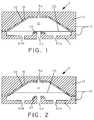
- FIG. 1is a cross-sectional side view of an illustrative normally closed valve in accordance with an embodiment of the present invention.
- FIG. 2is a cross-sectional side view of the valve of FIG. 1 in an open position.
- FIG. 3is a cross-sectional side view of a valve stator in accordance with an embodiment of the present invention.
- FIG. 4is a bottom view of a valve stator in accordance with an embodiment of the invention.
- FIG. 5is a schematic cross-sectional view of an injection mold in accordance with an embodiment of the invention.
- FIG. 6is a cross-sectional side view of a multilayered structure in accordance with an embodiment of the invention.
- FIG. 7is a schematic illustration of an injection mold with a multilayered structure disposed therein in accordance with an embodiment of the invention.
- FIG. 1is a cross-sectional side view of one type of valve 5 made in accordance with an embodiment of the present invention.
- the valve 5is of a type that is normally closed.
- the valve 5has a body 10 with an upper body portion 13 and a lower body portion 11 .
- the upper body portion 13includes a chamber wall 16 .
- the chamber wall 16defines a valve chamber 12 .
- a first port 42(e.g. inlet port) extends through the lower body portion 11 into the valve chamber 12 .
- a diaphragm 20is mounted within the chamber 12 .
- the diaphragm 20is spaced from the lower body portion 11 except along a valve seat 23 , which extends around the first port 42 .
- the lower body portion 11defines one or more output ports 82 a and 82 b .
- the diaphragm 20can be configured so that the diaphragm 20 covers the valve seat 23 and restricts fluid flow through the first port 42 and out the output ports 82 a and 82 b .
- the diaphragm 20includes one or more electrodes, which can extend to the edges of the chamber 12 .
- the one or more electrodes of the diaphragm 20are surrounded or encapsulated in a dielectric material or layer.
- the chamber wall 16includes one or more stationary electrodes, such as electrode 30 .
- the chamber wall 16 and the diaphragm 20can be configured so that, in the un-activated state, the separation distance between the stationary electrode 30 and the electrode of the diaphragm 20 is smaller near the edges of the chamber 12 .
- FIG. 2when a voltage is applied between the electrode of the diaphragm 20 and the stationary electrode 30 , the diaphragm 20 is drawn toward the chamber wall 16 in a rolling action such that the portions of the diaphragm 20 near the edges of the chamber wall 16 are drawn toward the chamber wall 16 first, followed by portions of the diaphragm farther away from the edges of the chamber wall 16 .
- Such a rolling actioncan improve efficiency and reduce the voltage requirements of the valve.
- the diaphragm 20When the diaphragm 20 is electrostatically actuated and pulled toward the chamber wall 16 , the diaphragm can move away from the valve seat 23 and uncover the first port 42 . This can allow fluid to flow between the first port 42 and the output ports 82 a and 82 b.
- One or more back pressure relief ports or vent openings 94may be provided in the upper body portion 13 to relieve any back pressure that might arise because of displacement of the diaphragm 20 .
- the diaphragm 20may become elastically deformed when electrostatically pulled toward the chamber wall 16 .
- the diaphragm 20may return to the un-activated first position under elastic restoring forces when the activation voltage is removed or reduced between the electrode of the diaphragm 20 and the electrode 30 of the chamber wall 16 .
- the diaphragm 20may only need to be electrostatically actuated in one direction, with the elastic restoring forces returning the diaphragm 20 to the original un-actuated state.
- the upper body portion 13 and lower body portion 11may be made from any suitable semi-rigid or rigid material, such as plastic, ceramic, silicon, etc.
- upper body portion 13 and lower body portion 11are constructed by molding a high temperature plastic such as ULTEM-1000TM (available from General Electric Company, Pittsfield, Mass.), CELAZOLETM (available from Hoechst-Celanese Corporation, Summit, N.J.), KETRONTM (available from Polymer Corporation, Reading, Pa.), or the like.
- valve 5 shown in FIGS. 1 and 2is only one example of a valve configuration that may be made in accordance with embodiments of the invention, but that many other components and configurations are contemplated herein.
- embodiments of the inventioncan be used to make components for valves that are normally open, valves having different shapes, electrostatically actuated pumps, and the like.
- stator 7in an electrostatically actuating valve structure. It will be appreciated that the stator 7 can be manufactured in various ways. In some embodiments of the invention, the stator 7 is manufactured using an injection molding process.
- Injection moldinginvolves injecting molten plastic into a mold at high pressure; the mold being the inverse of the desired shape.
- Many different types of injection molding machinescan be used.
- One example of an injection molding machine that can be usedis the Sumitomo SE7M, available from Sumitomo Plastics Machinery, Norcross, Ga.
- resin pelletsare poured into a feed hopper, which feeds the granules down to a screw or auger.
- the screwis turned by a hydraulic or electric motor that turns the screw feeding the pellets up the screw's grooves.
- the pelletsare moved forward in the screw and they undergo extreme pressure and friction which generates most of the heat needed to melt the pellets. Heaters on either side of the screw assist in the heating and temperature control around the pellets during the melting process.
- the molten materialis then forced into the mold under pressure and fills up a cavity inside the mold. The material is then allowed to cool and solidifies creating the part.
- FIG. 4is a bottom view of a valve stator in accordance with an embodiment of the invention.
- the electrode 30is shown with a vent opening 94 in the middle of a domed portion 32 .
- a plurality of post holes 34are present and configured to receive corresponding posts that can help hold the valve structure together.
- FIG. 5shows an injection mold 100 that can be used in some embodiments of the invention.
- the injection mold 100includes a top half 102 (core half) and a bottom half 104 (cavity half).
- the top half 102 and the bottom half 104enclose a molding cavity 106 .
- the molding cavity 106can have walls that are slightly angled to facilitate removal of parts from the mold 100 .
- the top half 102defines an injection port 108 .
- the bottom halfincludes an interior surface 110 and a dome 112 (not to scale). Molten material which is injected into the mold 100 will take the shape of the molding cavity 106 .
- the top half 102 and the bottom half 104can be separated from one another in order to facilitate removal of the resulting molded part.
- the stator 7can include an electrode 30 .
- the electrode 30can be covered by a layer of dielectric material.
- the electrode 30may be disposed onto the chamber wall 16 in various ways. For example, the electrode 30 could be affixed onto the chamber wall 16 with an adhesive, or it could be painted, sprayed, or dip coated onto the chamber wall 16 .
- an electrode 30is disposed onto the chamber wall 16 by first positioning a multilayered structure, including a conductive layer, within an injection mold and then injecting a molten polymer to form the stator.
- This type of processcan be referred to as insert injection molding.
- FIG. 6shows an exemplary multilayered structure 200 that can be used in an injection molding method of the invention.
- the multilayered structure 200can include a dielectric layer 202 disposed over a conductive layer 204 .
- the dielectric layer 202can serve as an insulator between the conductive layer 204 and the electrode on the diaphragm. As such, in an embodiment, the dielectric layer 202 extends continuously over the conductive layer 204 .
- the conductive layer 204can, in turn, be disposed over a polymeric support layer 206 .
- the polymeric support layer 206can serve as a substrate for deposition of the conductive layer 204 and can facilitate sufficient attachment of the multilayered structure 200 to the chamber wall 16 .
- the multilayered structure 200can define one or more apertures to accommodate various features such as the one or more back pressure relief ports or vent openings 94 in the upper body portion 13 .
- a multilayered structure 200is shown disposed within the cavity 306 of a mold 300 .
- the multilayered structure 200is positioned against the interior surface 310 of the bottom half 304 of the mold 300 .
- the multilayered structure 200is positioned with the dielectric layer 202 adjacent to the interior surface 310 so that the polymeric support layer 206 is facing the cavity 306 .
- Molten materialcan then pass into the cavity 306 through an injection port 308 and then be solidified to form a molded stator.
- the heat from the molten materialcan cause the polymeric support layer 206 to partially melt and form a tight bond with the molten material as it solidifies.
- the polymeric support layer 206 of the multilayered structure 200may be formed in various ways.
- the polymeric support layer 206is formed by an extrusion process.
- a thermoplastic polymersuch as such as ULTEM-1000TM (polyetherimide) (available from General Electric Company, Pittsfield, Mass.) or KAPTONTM (available from DuPont Electronic Technologies, Circleville, Ohio) can be extruded to form a continuous sheet or layer that serves as the polymeric support layer 206 .
- the polymeric support layer 206should be sufficiently thick so as to provide a suitable substrate for the deposition of the conductive layer 204 .
- the polymeric support layer 206should be sufficiently thin so as to not reduce the flexibility of the multilayered structure 200 too much.
- the polymeric support layer 206is between about 10 microns to about 100 microns thick. In various embodiments, the polymeric support layer 206 is about 30, 40, 50, 60, or 70 microns thick.
- the conductive layer 204may be formed by printing, plating or electron beam-physical vapor deposition (EB-PVD) of metal. In some cases, the conductive layer 204 may be patterned using a dry film resist. In an embodiment, the conductive layer 204 is deposited onto the support layer 206 using thermal evaporation techniques under vacuum. In an embodiment, the conductive layer 204 extends continuously over the polymeric support layer 206 . Various techniques can be used to increase the adhesion between the conductive layer 204 and the polymeric support layer 206 . In an embodiment, the support layer 206 is plasma-treated before the conductive layer 204 is applied.
- E-PVDelectron beam-physical vapor deposition
- the conductive layer 204will have surface roughness similar to the surface roughness of the underlying support layer 206 .
- the support layer 206has a surface root mean square (Rq) roughness of less than about 1000 angstroms. In an embodiment, the support layer 206 has a surface roughness (Rq) of greater than about 100 angstroms. In an embodiment, the support layer 206 has a surface roughness (Rq) of between about 100 angstroms and 1000 angstroms.
- the conductive layer 204can include many different materials.
- the conductive layer 204includes a metal.
- Exemplary metalscan include gold, platinum, copper, aluminum, and the like.
- the metalis of a high purity.
- the metalcan be about 99.99% pure.
- the metalis about 99.999% pure, 99.9999% pure, or even 99.99999% pure.
- the conductive layer 204can be from about 50 to about 500 angstroms thick. In an embodiment, the conductive layer can be about 100, 200, or 300 angstroms thick.
- the conductive layercan have a resistivity that is appropriate for configuration as an electrode on the stator. In an embodiment, the resistivity of the conductive layer is 10, 8, 6, 4, or 2 Ohms/square or lower.
- the roughness of the conductive layer 204can affect the adherence of the dielectric layer 202 to the conductive layer 204 .
- Surface roughnesscan be measured using equipment such as the DekTak line profilometer (available from Veeco Instruments Inc., Woobury, N.Y.) which drags a stylus along the surface of a test substrate for a distance such as a 1 millimeter length.
- One standard measure of roughness that can be automatically calculated by line profilometers(such as the DekTak) is the root mean square roughness (Rq).
- the Rq roughnessis the root mean square average of the departures of the roughness profile from the mean line. Rq roughness is also defined in ANSI B46.1.
- a surface roughness (Rq) on the conductive layer 204 of less than about 100 angstromscan lead to insufficient adhesion between the dielectric layer 202 and the conductive layer 204 .
- a surface roughness (Rq) of greater than about 1000 angstromscan result in making the dielectric layer 202 too rough for reliable and consistent actuation of the valve.
- the conductive layer 204has a surface roughness (Rq) of less than about 1000 angstroms.
- the conductive layer 204has a surface roughness (Rq) of greater than about 100 angstroms.
- the conductive layer 204has a surface roughness (Rq) of between about 100 angstroms and 1000 angstroms.
- the dielectric layer 202is adhered to the conductive layer 204 with sufficient strength to resist separation from the conductive layer 204 during repeated actuation of an electrostatic valve.
- the dielectric layer 202can be deposited onto the conductive layer 204 using a variety of techniques. In some embodiments, it can be spray coated, roller coated, dip coated, or applied using a variety of printing techniques. In some embodiments, the dielectric layer is applied using a flash evaporation technique. In some embodiments, the dielectric layer is subjected to UV light treatment after application in order to cure the dielectric layer.
- the dielectric layer 202will have surface roughness similar to the surface roughness of the underlying conductive layer 204 .
- the dielectric layer 202has a surface roughness (Rq) of less than about 1000 angstroms. In an embodiment, the dielectric layer 202 has a surface roughness (Rq) of greater than about 100 angstroms. In an embodiment, the dielectric layer 202 has a surface roughness (Rq) of between about 100 angstroms and 1000 angstroms.
- the dielectric layer 202is on the surface of the stator 7 facing the valve chamber 12 .
- the electrostatic valvedepends on a rolling action for actuation, surface defects on the dielectric layer 202 can adversely affect the performance of the valve and in some cases cause it to cease actuating. Accordingly, in an embodiment, the dielectric layer 202 is substantially free of surface defects.
- the dielectric layer 202can include a variety of materials.
- the dielectric layer 202can include oxides, such as aluminum oxide.
- the dielectric layer 202includes one or more polymers. It will be appreciated that various polymers have dielectric properties.
- the dielectric layercan include polymers such as fluoropolymers (such as PTFE and fluoroacrylates), acrylate polymers, polysiloxanes (silicone), polyimides (such as polymethylglutarimide), parylene and the like.
- the dielectric properties of a materialmay be gauged by its dielectric constant.
- the dielectric layershould have sufficient dielectric properties to be able to insulate the conductive layer from the electrode of the diaphragm.
- the material of the dielectric layercan have a dielectric constant of between about 3.0 and about 4.0.
- the material of the dielectric layercan have a dielectric constant of about 3.5.
- the dielectric properties of the dielectric layerare also influenced by the thickness of the dielectric layer.
- the dielectric layeris between about 0.1 microns and about 5 microns. In a particular embodiment, the dielectric layer is between about 0.45 and about 0.55 microns thick.
- the surface energy of the dielectric layercan affect how easily the diaphragm releases from the electrode on the chamber wall of the valve. In an embodiment, the surface energy of the dielectric layer is less than or equal to about 30 dynes per centimeter.
Landscapes
- Engineering & Computer Science (AREA)
- General Engineering & Computer Science (AREA)
- Mechanical Engineering (AREA)
- Manufacturing & Machinery (AREA)
- Injection Moulding Of Plastics Or The Like (AREA)
Abstract
Description
Claims (26)
Priority Applications (1)
| Application Number | Priority Date | Filing Date | Title |
|---|---|---|---|
| US11/458,718US8007704B2 (en) | 2006-07-20 | 2006-07-20 | Insert molded actuator components |
Applications Claiming Priority (1)
| Application Number | Priority Date | Filing Date | Title |
|---|---|---|---|
| US11/458,718US8007704B2 (en) | 2006-07-20 | 2006-07-20 | Insert molded actuator components |
Publications (2)
| Publication Number | Publication Date |
|---|---|
| US20080029207A1 US20080029207A1 (en) | 2008-02-07 |
| US8007704B2true US8007704B2 (en) | 2011-08-30 |
Family
ID=39028003
Family Applications (1)
| Application Number | Title | Priority Date | Filing Date |
|---|---|---|---|
| US11/458,718Active2029-07-02US8007704B2 (en) | 2006-07-20 | 2006-07-20 | Insert molded actuator components |
Country Status (1)
| Country | Link |
|---|---|
| US (1) | US8007704B2 (en) |
Cited By (6)
| Publication number | Priority date | Publication date | Assignee | Title |
|---|---|---|---|---|
| US20090190290A1 (en)* | 2008-01-24 | 2009-07-30 | Stephen Brian Lynch | Methods and Systems for Forming Housings From Multi-Layer Materials |
| US20140217523A1 (en)* | 2011-07-29 | 2014-08-07 | Epcos Ag | Housing for a Semiconductor Chip and Semiconductor Chip with a Housing |
| US20150266092A1 (en)* | 2012-09-28 | 2015-09-24 | Siemens Aktiengesellschaft | Hybride part and method of manufacture |
| US20170097108A1 (en)* | 2015-10-01 | 2017-04-06 | Corporation For National Research Initiatives | Three-Way Microvalve device and method of fabrication |
| US20170298966A1 (en)* | 2016-04-14 | 2017-10-19 | Los Alamos National Security, Llc | Magnetically controlled valve and pump devices and methods of using the same |
| US20190203703A1 (en)* | 2016-09-13 | 2019-07-04 | Albert-Ludwigs-Universität Freiburg | Micro Valve, Fluid Pump, And Method Of Operating A Fluid Pump |
Citations (106)
| Publication number | Priority date | Publication date | Assignee | Title |
|---|---|---|---|---|
| US2403692A (en) | 1944-12-29 | 1946-07-09 | George C Tibbetts | Piezoelectric device |
| US2975307A (en) | 1958-01-02 | 1961-03-14 | Ibm | Capacitive prime mover |
| US3304446A (en) | 1963-12-26 | 1967-02-14 | Union Oil Co | Electrostrictive fluid transducer |
| US3381623A (en) | 1966-04-26 | 1968-05-07 | Harold F Elliott | Electromagnetic reciprocating fluid pump |
| US3414010A (en) | 1965-11-01 | 1968-12-03 | Honeywell Inc | Control apparatus |
| US3641373A (en) | 1968-10-08 | 1972-02-08 | Proctor Ets | Electrostatic system for generating periodical mechanical vibrations |
| US3803424A (en) | 1972-05-08 | 1974-04-09 | Physics Int Co | Piezoelectric pump system |
| US3947644A (en) | 1971-08-20 | 1976-03-30 | Kureha Kagaku Kogyo Kabushiki Kaisha | Piezoelectric-type electroacoustic transducer |
| US4115036A (en) | 1976-03-01 | 1978-09-19 | U.S. Philips Corporation | Pump for pumping liquid in a pulse-free flow |
| US4140936A (en) | 1977-09-01 | 1979-02-20 | The United States Of America As Represented By The Secretary Of The Navy | Square and rectangular electroacoustic bender bar transducer |
| US4197737A (en) | 1977-05-10 | 1980-04-15 | Applied Devices Corporation | Multiple sensing device and sensing devices therefor |
| SU744877A1 (en) | 1978-01-09 | 1980-06-30 | Институт математики СО АН СССР | Electrostatic motor of reciprocal motion |
| US4415607A (en) | 1982-09-13 | 1983-11-15 | Allen-Bradley Company | Method of manufacturing printed circuit network devices |
| US4418886A (en) | 1981-03-07 | 1983-12-06 | Walter Holzer | Electro-magnetic valves particularly for household appliances |
| US4453169A (en) | 1982-04-07 | 1984-06-05 | Exxon Research And Engineering Co. | Ink jet apparatus and method |
| US4478076A (en) | 1982-09-30 | 1984-10-23 | Honeywell Inc. | Flow sensor |
| US4478077A (en) | 1982-09-30 | 1984-10-23 | Honeywell Inc. | Flow sensor |
| US4498850A (en) | 1980-04-28 | 1985-02-12 | Gena Perlov | Method and device for fluid transfer |
| US4501144A (en) | 1982-09-30 | 1985-02-26 | Honeywell Inc. | Flow sensor |
| US4539575A (en) | 1983-06-06 | 1985-09-03 | Siemens Aktiengesellschaft | Recorder operating with liquid drops and comprising elongates piezoelectric transducers rigidly connected at both ends with a jet orifice plate |
| US4576050A (en) | 1984-08-29 | 1986-03-18 | General Motors Corporation | Thermal diffusion fluid flow sensor |
| US4581624A (en) | 1984-03-01 | 1986-04-08 | Allied Corporation | Microminiature semiconductor valve |
| US4651564A (en) | 1982-09-30 | 1987-03-24 | Honeywell Inc. | Semiconductor device |
| US4654546A (en) | 1984-11-20 | 1987-03-31 | Kari Kirjavainen | Electromechanical film and procedure for manufacturing same |
| US4710419A (en) | 1984-07-16 | 1987-12-01 | Gregory Vernon C | In-mold process for fabrication of molded plastic printed circuit boards |
| US4722360A (en) | 1985-01-26 | 1988-02-02 | Shoketsu Kinzoku Kogyo Kabushiki Kaisha | Fluid regulator |
| US4756508A (en) | 1985-02-21 | 1988-07-12 | Ford Motor Company | Silicon valve |
| US4821999A (en) | 1987-01-22 | 1989-04-18 | Tokyo Electric Co., Ltd. | Valve element and process of producing the same |
| US4898200A (en) | 1984-05-01 | 1990-02-06 | Shoketsu Kinzohu Kogyo Kabushiki Kaisha | Electropneumatic transducer |
| US4911616A (en) | 1988-01-19 | 1990-03-27 | Laumann Jr Carl W | Micro miniature implantable pump |
| US4912288A (en) | 1985-09-04 | 1990-03-27 | Allen-Bradley International Limited | Moulded electric circuit package |
| US4938742A (en) | 1988-02-04 | 1990-07-03 | Smits Johannes G | Piezoelectric micropump with microvalves |
| US4939405A (en) | 1987-12-28 | 1990-07-03 | Misuzuerie Co. Ltd. | Piezo-electric vibrator pump |
| US4944087A (en) | 1988-10-05 | 1990-07-31 | Rogers Corporation | Method of making a curved plastic body with circuit pattern |
| US4985601A (en) | 1989-05-02 | 1991-01-15 | Hagner George R | Circuit boards with recessed traces |
| US4996391A (en) | 1988-09-30 | 1991-02-26 | Siemens Aktiengesellschaft | Printed circuit board having an injection molded substrate |
| US5008496A (en) | 1988-09-15 | 1991-04-16 | Siemens Aktiengesellschaft | Three-dimensional printed circuit board |
| US5065978A (en) | 1988-04-27 | 1991-11-19 | Dragerwerk Aktiengesellschaft | Valve arrangement of microstructured components |
| US5069419A (en) | 1989-06-23 | 1991-12-03 | Ic Sensors Inc. | Semiconductor microactuator |
| US5078581A (en) | 1989-08-07 | 1992-01-07 | International Business Machines Corporation | Cascade compressor |
| US5082242A (en) | 1989-12-27 | 1992-01-21 | Ulrich Bonne | Electronic microvalve apparatus and fabrication |
| US5085562A (en) | 1989-04-11 | 1992-02-04 | Westonbridge International Limited | Micropump having a constant output |
| US5096388A (en) | 1990-03-22 | 1992-03-17 | The Charles Stark Draper Laboratory, Inc. | Microfabricated pump |
| US5130499A (en) | 1990-04-27 | 1992-07-14 | E. I. Du Pont De Nemours And Company | Flexible circuit and a device for holding the flexible circuit in the folded state |
| US5129794A (en) | 1990-10-30 | 1992-07-14 | Hewlett-Packard Company | Pump apparatus |
| US5148074A (en) | 1988-08-31 | 1992-09-15 | Seikosha Co., Ltd. | Piezoelectric device and related converting devices |
| US5153385A (en) | 1991-03-18 | 1992-10-06 | Motorola, Inc. | Transfer molded semiconductor package with improved adhesion |
| US5171132A (en) | 1989-12-27 | 1992-12-15 | Seiko Epson Corporation | Two-valve thin plate micropump |
| US5176358A (en) | 1991-08-08 | 1993-01-05 | Honeywell Inc. | Microstructure gas valve control |
| US5180288A (en) | 1989-08-03 | 1993-01-19 | Fraunhofer-Gesellschaft Zur Forderung Der Angewandten Forschung E.V. | Microminiaturized electrostatic pump |
| US5180623A (en) | 1989-12-27 | 1993-01-19 | Honeywell Inc. | Electronic microvalve apparatus and fabrication |
| US5192197A (en) | 1991-11-27 | 1993-03-09 | Rockwell International Corporation | Piezoelectric pump |
| US5206557A (en) | 1990-11-27 | 1993-04-27 | Mcnc | Microelectromechanical transducer and fabrication method |
| US5220489A (en) | 1991-10-11 | 1993-06-15 | Motorola, Inc. | Multicomponent integrated circuit package |
| US5220488A (en) | 1985-09-04 | 1993-06-15 | Ufe Incorporated | Injection molded printed circuits |
| US5219278A (en) | 1989-11-10 | 1993-06-15 | Westonbridge International, Ltd. | Micropump with improved priming |
| US5224843A (en) | 1989-06-14 | 1993-07-06 | Westonbridge International Ltd. | Two valve micropump with improved outlet |
| US5241454A (en) | 1992-01-22 | 1993-08-31 | International Business Machines Corporation | Mutlilayered flexible circuit package |
| US5241133A (en) | 1990-12-21 | 1993-08-31 | Motorola, Inc. | Leadless pad array chip carrier |
| US5244527A (en) | 1991-08-06 | 1993-09-14 | Nec Corporation | Manufacturing unit for semiconductor devices |
| US5244537A (en) | 1989-12-27 | 1993-09-14 | Honeywell, Inc. | Fabrication of an electronic microvalve apparatus |
| US5253010A (en) | 1988-05-13 | 1993-10-12 | Minolta Camera Kabushiki Kaisha | Printed circuit board |
| EP0253892B1 (en) | 1985-12-28 | 1994-04-06 | Nissha Printing Co., Ltd. | Transfer material for printed circuit board and printed circuit board prepared using said transfer material and process for preparation thereof |
| US5322258A (en) | 1989-04-28 | 1994-06-21 | Messerschmitt-Bolkow-Blohm Gmbh | Micromechanical actuator |
| US5325880A (en) | 1993-04-19 | 1994-07-05 | Tini Alloy Company | Shape memory alloy film actuated microvalve |
| US5441597A (en) | 1992-12-01 | 1995-08-15 | Honeywell Inc. | Microstructure gas valve control forming method |
| US5452878A (en) | 1991-06-18 | 1995-09-26 | Danfoss A/S | Miniature actuating device |
| US5499909A (en) | 1993-11-17 | 1996-03-19 | Aisin Seiki Kabushiki Kaisha Of Kariya | Pneumatically driven micro-pump |
| US5541465A (en) | 1992-08-25 | 1996-07-30 | Kanagawa Academy Of Science And Technology | Electrostatic actuator |
| US5552654A (en) | 1993-10-21 | 1996-09-03 | Mitsubishi Chemical Corporation | Electrostatic actuator |
| US5571401A (en) | 1995-03-27 | 1996-11-05 | California Institute Of Technology | Sensor arrays for detecting analytes in fluids |
| EP0744821A2 (en) | 1995-05-26 | 1996-11-27 | Asmo Co., Ltd. | Electrostatic actuator with different electrode spacing |
| US5642015A (en) | 1993-07-14 | 1997-06-24 | The University Of British Columbia | Elastomeric micro electro mechanical systems |
| DE19617852A1 (en) | 1996-04-23 | 1997-10-30 | Karlsruhe Forschzent | Process for the planar production of pneumatic and fluidic miniature manipulators |
| US5683159A (en) | 1997-01-03 | 1997-11-04 | Johnson; Greg P. | Hardware mounting rail |
| US5725363A (en) | 1994-01-25 | 1998-03-10 | Forschungszentrum Karlsruhe Gmbh | Micromembrane pump |
| US5759015A (en) | 1993-12-28 | 1998-06-02 | Westonbridge International Limited | Piezoelectric micropump having actuation electrodes and stopper members |
| US5759014A (en) | 1994-01-14 | 1998-06-02 | Westonbridge International Limited | Micropump |
| US5822170A (en) | 1997-10-09 | 1998-10-13 | Honeywell Inc. | Hydrophobic coating for reducing humidity effect in electrostatic actuators |
| US5836750A (en) | 1997-10-09 | 1998-11-17 | Honeywell Inc. | Electrostatically actuated mesopump having a plurality of elementary cells |
| US5863708A (en) | 1994-11-10 | 1999-01-26 | Sarnoff Corporation | Partitioned microelectronic device array |
| US5901939A (en) | 1997-10-09 | 1999-05-11 | Honeywell Inc. | Buckled actuator with enhanced restoring force |
| US5911872A (en) | 1996-08-14 | 1999-06-15 | California Institute Of Technology | Sensors for detecting analytes in fluids |
| US5941501A (en)* | 1996-09-06 | 1999-08-24 | Xerox Corporation | Passively addressable cantilever valves |
| US5954079A (en) | 1996-04-30 | 1999-09-21 | Hewlett-Packard Co. | Asymmetrical thermal actuation in a microactuator |
| US6040529A (en) | 1997-02-19 | 2000-03-21 | Alps Electric Co., Ltd. | Flexible substrate |
| US6106245A (en) | 1997-10-09 | 2000-08-22 | Honeywell | Low cost, high pumping rate electrostatically actuated mesopump |
| US6160962A (en) | 1996-01-26 | 2000-12-12 | Asahi Kogaku Kogyo Kaisha | Camera with lens barrier apparatus |
| US6179586B1 (en) | 1999-09-15 | 2001-01-30 | Honeywell International Inc. | Dual diaphragm, single chamber mesopump |
| US6184607B1 (en) | 1998-12-29 | 2001-02-06 | Honeywell International Inc. | Driving strategy for non-parallel arrays of electrostatic actuators sharing a common electrode |
| US6182941B1 (en) | 1998-10-28 | 2001-02-06 | Festo Ag & Co. | Micro-valve with capacitor plate position detector |
| US6215221B1 (en) | 1998-12-29 | 2001-04-10 | Honeywell International Inc. | Electrostatic/pneumatic actuators for active surfaces |
| US6240944B1 (en) | 1999-09-23 | 2001-06-05 | Honeywell International Inc. | Addressable valve arrays for proportional pressure or flow control |
| US6288343B1 (en) | 1998-10-08 | 2001-09-11 | Samsung Electronics Co., Ltd. | Printed circuit board |
| US6307751B1 (en) | 1998-06-01 | 2001-10-23 | Wearlogic, Inc. | Flexible circuit assembly |
| US6320137B1 (en) | 2000-04-11 | 2001-11-20 | 3M Innovative Properties Company | Flexible circuit with coverplate layer and overlapping protective layer |
| US20030136576A1 (en) | 2001-11-09 | 2003-07-24 | Nexans | Printed circuit support having integrated connections and process for manufacturing such a support |
| US6675470B2 (en) | 1998-08-18 | 2004-01-13 | Seiko Epson Corporation | Method for manufacturing an electro-optical device |
| US6768654B2 (en)* | 2000-09-18 | 2004-07-27 | Wavezero, Inc. | Multi-layered structures and methods for manufacturing the multi-layered structures |
| US6837476B2 (en) | 2002-06-19 | 2005-01-04 | Honeywell International Inc. | Electrostatically actuated valve |
| US20050001767A1 (en)* | 2003-07-03 | 2005-01-06 | Thomas Wulff | Insert molded antenna |
| US20050011668A1 (en) | 2003-07-16 | 2005-01-20 | Samsung Electronics Co., Ltd. | Thin printed circuit board for manufacturing chip scale package |
| US6858921B2 (en) | 2002-12-26 | 2005-02-22 | Sumitomo Electric Industries, Ltd. | Flexible printed circuit substrate |
| US20050122700A1 (en) | 2003-12-09 | 2005-06-09 | Kim Deok-Heung | Flexible printed circuit board |
| US6915566B2 (en) | 1999-03-01 | 2005-07-12 | Texas Instruments Incorporated | Method of fabricating flexible circuits for integrated circuit interconnections |
| US20070257398A1 (en)* | 2006-05-04 | 2007-11-08 | Moncrieff Scott E | Laminated electronic components for insert molding |
Family Cites Families (1)
| Publication number | Priority date | Publication date | Assignee | Title |
|---|---|---|---|---|
| US6106246A (en)* | 1998-10-05 | 2000-08-22 | Trebor International, Inc. | Free-diaphragm pump |
- 2006
- 2006-07-20USUS11/458,718patent/US8007704B2/enactiveActive
Patent Citations (112)
| Publication number | Priority date | Publication date | Assignee | Title |
|---|---|---|---|---|
| US2403692A (en) | 1944-12-29 | 1946-07-09 | George C Tibbetts | Piezoelectric device |
| US2975307A (en) | 1958-01-02 | 1961-03-14 | Ibm | Capacitive prime mover |
| US3304446A (en) | 1963-12-26 | 1967-02-14 | Union Oil Co | Electrostrictive fluid transducer |
| US3414010A (en) | 1965-11-01 | 1968-12-03 | Honeywell Inc | Control apparatus |
| US3381623A (en) | 1966-04-26 | 1968-05-07 | Harold F Elliott | Electromagnetic reciprocating fluid pump |
| US3641373A (en) | 1968-10-08 | 1972-02-08 | Proctor Ets | Electrostatic system for generating periodical mechanical vibrations |
| US3769531A (en) | 1968-10-08 | 1973-10-30 | Proctor Ets | Electrostatic system for generating periodical mechanical vibrations |
| US3947644A (en) | 1971-08-20 | 1976-03-30 | Kureha Kagaku Kogyo Kabushiki Kaisha | Piezoelectric-type electroacoustic transducer |
| US3803424A (en) | 1972-05-08 | 1974-04-09 | Physics Int Co | Piezoelectric pump system |
| US4115036A (en) | 1976-03-01 | 1978-09-19 | U.S. Philips Corporation | Pump for pumping liquid in a pulse-free flow |
| US4197737A (en) | 1977-05-10 | 1980-04-15 | Applied Devices Corporation | Multiple sensing device and sensing devices therefor |
| US4140936A (en) | 1977-09-01 | 1979-02-20 | The United States Of America As Represented By The Secretary Of The Navy | Square and rectangular electroacoustic bender bar transducer |
| SU744877A1 (en) | 1978-01-09 | 1980-06-30 | Институт математики СО АН СССР | Electrostatic motor of reciprocal motion |
| US4498850A (en) | 1980-04-28 | 1985-02-12 | Gena Perlov | Method and device for fluid transfer |
| US4418886A (en) | 1981-03-07 | 1983-12-06 | Walter Holzer | Electro-magnetic valves particularly for household appliances |
| US4453169A (en) | 1982-04-07 | 1984-06-05 | Exxon Research And Engineering Co. | Ink jet apparatus and method |
| US4415607A (en) | 1982-09-13 | 1983-11-15 | Allen-Bradley Company | Method of manufacturing printed circuit network devices |
| US4478076A (en) | 1982-09-30 | 1984-10-23 | Honeywell Inc. | Flow sensor |
| US4478077A (en) | 1982-09-30 | 1984-10-23 | Honeywell Inc. | Flow sensor |
| US4501144A (en) | 1982-09-30 | 1985-02-26 | Honeywell Inc. | Flow sensor |
| US4651564A (en) | 1982-09-30 | 1987-03-24 | Honeywell Inc. | Semiconductor device |
| US4539575A (en) | 1983-06-06 | 1985-09-03 | Siemens Aktiengesellschaft | Recorder operating with liquid drops and comprising elongates piezoelectric transducers rigidly connected at both ends with a jet orifice plate |
| US4581624A (en) | 1984-03-01 | 1986-04-08 | Allied Corporation | Microminiature semiconductor valve |
| US4898200A (en) | 1984-05-01 | 1990-02-06 | Shoketsu Kinzohu Kogyo Kabushiki Kaisha | Electropneumatic transducer |
| US4710419A (en) | 1984-07-16 | 1987-12-01 | Gregory Vernon C | In-mold process for fabrication of molded plastic printed circuit boards |
| US4576050A (en) | 1984-08-29 | 1986-03-18 | General Motors Corporation | Thermal diffusion fluid flow sensor |
| US4654546A (en) | 1984-11-20 | 1987-03-31 | Kari Kirjavainen | Electromechanical film and procedure for manufacturing same |
| US4722360A (en) | 1985-01-26 | 1988-02-02 | Shoketsu Kinzoku Kogyo Kabushiki Kaisha | Fluid regulator |
| US4756508A (en) | 1985-02-21 | 1988-07-12 | Ford Motor Company | Silicon valve |
| US5003693A (en) | 1985-09-04 | 1991-04-02 | Allen-Bradley International Limited | Manufacture of electrical circuits |
| US5220488A (en) | 1985-09-04 | 1993-06-15 | Ufe Incorporated | Injection molded printed circuits |
| US4912288A (en) | 1985-09-04 | 1990-03-27 | Allen-Bradley International Limited | Moulded electric circuit package |
| EP0253892B1 (en) | 1985-12-28 | 1994-04-06 | Nissha Printing Co., Ltd. | Transfer material for printed circuit board and printed circuit board prepared using said transfer material and process for preparation thereof |
| US4821999A (en) | 1987-01-22 | 1989-04-18 | Tokyo Electric Co., Ltd. | Valve element and process of producing the same |
| US4939405A (en) | 1987-12-28 | 1990-07-03 | Misuzuerie Co. Ltd. | Piezo-electric vibrator pump |
| US4911616A (en) | 1988-01-19 | 1990-03-27 | Laumann Jr Carl W | Micro miniature implantable pump |
| US4938742A (en) | 1988-02-04 | 1990-07-03 | Smits Johannes G | Piezoelectric micropump with microvalves |
| US5065978A (en) | 1988-04-27 | 1991-11-19 | Dragerwerk Aktiengesellschaft | Valve arrangement of microstructured components |
| US5253010A (en) | 1988-05-13 | 1993-10-12 | Minolta Camera Kabushiki Kaisha | Printed circuit board |
| US5148074A (en) | 1988-08-31 | 1992-09-15 | Seikosha Co., Ltd. | Piezoelectric device and related converting devices |
| US5008496A (en) | 1988-09-15 | 1991-04-16 | Siemens Aktiengesellschaft | Three-dimensional printed circuit board |
| US4996391A (en) | 1988-09-30 | 1991-02-26 | Siemens Aktiengesellschaft | Printed circuit board having an injection molded substrate |
| US4944087A (en) | 1988-10-05 | 1990-07-31 | Rogers Corporation | Method of making a curved plastic body with circuit pattern |
| US5085562A (en) | 1989-04-11 | 1992-02-04 | Westonbridge International Limited | Micropump having a constant output |
| US5322258A (en) | 1989-04-28 | 1994-06-21 | Messerschmitt-Bolkow-Blohm Gmbh | Micromechanical actuator |
| US4985601A (en) | 1989-05-02 | 1991-01-15 | Hagner George R | Circuit boards with recessed traces |
| US5224843A (en) | 1989-06-14 | 1993-07-06 | Westonbridge International Ltd. | Two valve micropump with improved outlet |
| US5069419A (en) | 1989-06-23 | 1991-12-03 | Ic Sensors Inc. | Semiconductor microactuator |
| US5180288A (en) | 1989-08-03 | 1993-01-19 | Fraunhofer-Gesellschaft Zur Forderung Der Angewandten Forschung E.V. | Microminiaturized electrostatic pump |
| US5078581A (en) | 1989-08-07 | 1992-01-07 | International Business Machines Corporation | Cascade compressor |
| US5219278A (en) | 1989-11-10 | 1993-06-15 | Westonbridge International, Ltd. | Micropump with improved priming |
| US5180623A (en) | 1989-12-27 | 1993-01-19 | Honeywell Inc. | Electronic microvalve apparatus and fabrication |
| US5082242A (en) | 1989-12-27 | 1992-01-21 | Ulrich Bonne | Electronic microvalve apparatus and fabrication |
| US5171132A (en) | 1989-12-27 | 1992-12-15 | Seiko Epson Corporation | Two-valve thin plate micropump |
| US5244537A (en) | 1989-12-27 | 1993-09-14 | Honeywell, Inc. | Fabrication of an electronic microvalve apparatus |
| US5096388A (en) | 1990-03-22 | 1992-03-17 | The Charles Stark Draper Laboratory, Inc. | Microfabricated pump |
| US5130499A (en) | 1990-04-27 | 1992-07-14 | E. I. Du Pont De Nemours And Company | Flexible circuit and a device for holding the flexible circuit in the folded state |
| US5129794A (en) | 1990-10-30 | 1992-07-14 | Hewlett-Packard Company | Pump apparatus |
| US5206557A (en) | 1990-11-27 | 1993-04-27 | Mcnc | Microelectromechanical transducer and fabrication method |
| US5241133A (en) | 1990-12-21 | 1993-08-31 | Motorola, Inc. | Leadless pad array chip carrier |
| US5153385A (en) | 1991-03-18 | 1992-10-06 | Motorola, Inc. | Transfer molded semiconductor package with improved adhesion |
| US5452878A (en) | 1991-06-18 | 1995-09-26 | Danfoss A/S | Miniature actuating device |
| US5244527A (en) | 1991-08-06 | 1993-09-14 | Nec Corporation | Manufacturing unit for semiconductor devices |
| US5176358A (en) | 1991-08-08 | 1993-01-05 | Honeywell Inc. | Microstructure gas valve control |
| US5323999A (en) | 1991-08-08 | 1994-06-28 | Honeywell Inc. | Microstructure gas valve control |
| US5220489A (en) | 1991-10-11 | 1993-06-15 | Motorola, Inc. | Multicomponent integrated circuit package |
| US5192197A (en) | 1991-11-27 | 1993-03-09 | Rockwell International Corporation | Piezoelectric pump |
| US5241454A (en) | 1992-01-22 | 1993-08-31 | International Business Machines Corporation | Mutlilayered flexible circuit package |
| US5541465A (en) | 1992-08-25 | 1996-07-30 | Kanagawa Academy Of Science And Technology | Electrostatic actuator |
| US5441597A (en) | 1992-12-01 | 1995-08-15 | Honeywell Inc. | Microstructure gas valve control forming method |
| US5325880A (en) | 1993-04-19 | 1994-07-05 | Tini Alloy Company | Shape memory alloy film actuated microvalve |
| US5642015A (en) | 1993-07-14 | 1997-06-24 | The University Of British Columbia | Elastomeric micro electro mechanical systems |
| US5552654A (en) | 1993-10-21 | 1996-09-03 | Mitsubishi Chemical Corporation | Electrostatic actuator |
| US5499909A (en) | 1993-11-17 | 1996-03-19 | Aisin Seiki Kabushiki Kaisha Of Kariya | Pneumatically driven micro-pump |
| US5759015A (en) | 1993-12-28 | 1998-06-02 | Westonbridge International Limited | Piezoelectric micropump having actuation electrodes and stopper members |
| US5759014A (en) | 1994-01-14 | 1998-06-02 | Westonbridge International Limited | Micropump |
| US5725363A (en) | 1994-01-25 | 1998-03-10 | Forschungszentrum Karlsruhe Gmbh | Micromembrane pump |
| US5863708A (en) | 1994-11-10 | 1999-01-26 | Sarnoff Corporation | Partitioned microelectronic device array |
| US5571401A (en) | 1995-03-27 | 1996-11-05 | California Institute Of Technology | Sensor arrays for detecting analytes in fluids |
| EP0744821A2 (en) | 1995-05-26 | 1996-11-27 | Asmo Co., Ltd. | Electrostatic actuator with different electrode spacing |
| EP0744821A3 (en) | 1995-05-26 | 1996-12-04 | Asmo Co., Ltd. | Electrostatic actuator with different electrode spacing |
| US6160962A (en) | 1996-01-26 | 2000-12-12 | Asahi Kogaku Kogyo Kaisha | Camera with lens barrier apparatus |
| DE19617852A1 (en) | 1996-04-23 | 1997-10-30 | Karlsruhe Forschzent | Process for the planar production of pneumatic and fluidic miniature manipulators |
| US5954079A (en) | 1996-04-30 | 1999-09-21 | Hewlett-Packard Co. | Asymmetrical thermal actuation in a microactuator |
| US5911872A (en) | 1996-08-14 | 1999-06-15 | California Institute Of Technology | Sensors for detecting analytes in fluids |
| US5941501A (en)* | 1996-09-06 | 1999-08-24 | Xerox Corporation | Passively addressable cantilever valves |
| US5683159A (en) | 1997-01-03 | 1997-11-04 | Johnson; Greg P. | Hardware mounting rail |
| US6040529A (en) | 1997-02-19 | 2000-03-21 | Alps Electric Co., Ltd. | Flexible substrate |
| US5901939A (en) | 1997-10-09 | 1999-05-11 | Honeywell Inc. | Buckled actuator with enhanced restoring force |
| US6106245A (en) | 1997-10-09 | 2000-08-22 | Honeywell | Low cost, high pumping rate electrostatically actuated mesopump |
| US5836750A (en) | 1997-10-09 | 1998-11-17 | Honeywell Inc. | Electrostatically actuated mesopump having a plurality of elementary cells |
| US5822170A (en) | 1997-10-09 | 1998-10-13 | Honeywell Inc. | Hydrophobic coating for reducing humidity effect in electrostatic actuators |
| US6307751B1 (en) | 1998-06-01 | 2001-10-23 | Wearlogic, Inc. | Flexible circuit assembly |
| US6675470B2 (en) | 1998-08-18 | 2004-01-13 | Seiko Epson Corporation | Method for manufacturing an electro-optical device |
| US6288343B1 (en) | 1998-10-08 | 2001-09-11 | Samsung Electronics Co., Ltd. | Printed circuit board |
| US6182941B1 (en) | 1998-10-28 | 2001-02-06 | Festo Ag & Co. | Micro-valve with capacitor plate position detector |
| US6288472B1 (en) | 1998-12-29 | 2001-09-11 | Honeywell International Inc. | Electrostatic/pneumatic actuators for active surfaces |
| US6215221B1 (en) | 1998-12-29 | 2001-04-10 | Honeywell International Inc. | Electrostatic/pneumatic actuators for active surfaces |
| US6184607B1 (en) | 1998-12-29 | 2001-02-06 | Honeywell International Inc. | Driving strategy for non-parallel arrays of electrostatic actuators sharing a common electrode |
| US6915566B2 (en) | 1999-03-01 | 2005-07-12 | Texas Instruments Incorporated | Method of fabricating flexible circuits for integrated circuit interconnections |
| US6179586B1 (en) | 1999-09-15 | 2001-01-30 | Honeywell International Inc. | Dual diaphragm, single chamber mesopump |
| US6240944B1 (en) | 1999-09-23 | 2001-06-05 | Honeywell International Inc. | Addressable valve arrays for proportional pressure or flow control |
| US6320137B1 (en) | 2000-04-11 | 2001-11-20 | 3M Innovative Properties Company | Flexible circuit with coverplate layer and overlapping protective layer |
| US6768654B2 (en)* | 2000-09-18 | 2004-07-27 | Wavezero, Inc. | Multi-layered structures and methods for manufacturing the multi-layered structures |
| US20030136576A1 (en) | 2001-11-09 | 2003-07-24 | Nexans | Printed circuit support having integrated connections and process for manufacturing such a support |
| US6837476B2 (en) | 2002-06-19 | 2005-01-04 | Honeywell International Inc. | Electrostatically actuated valve |
| US6968862B2 (en) | 2002-06-19 | 2005-11-29 | Honeywell International Inc. | Electrostatically actuated valve |
| US6858921B2 (en) | 2002-12-26 | 2005-02-22 | Sumitomo Electric Industries, Ltd. | Flexible printed circuit substrate |
| US20050001767A1 (en)* | 2003-07-03 | 2005-01-06 | Thomas Wulff | Insert molded antenna |
| US20050011668A1 (en) | 2003-07-16 | 2005-01-20 | Samsung Electronics Co., Ltd. | Thin printed circuit board for manufacturing chip scale package |
| US20050122700A1 (en) | 2003-12-09 | 2005-06-09 | Kim Deok-Heung | Flexible printed circuit board |
| US20070257398A1 (en)* | 2006-05-04 | 2007-11-08 | Moncrieff Scott E | Laminated electronic components for insert molding |
Non-Patent Citations (25)
| Title |
|---|
| "Handbook of Physical Vapor Deposition (PVD) Processing", Mattox, D.M., 1998, William Andrew Publishing, pp. 92-100, 472-474, and 523-528. Accessed using www.knovel.com.* |
| "Large-Scale Linearization Circuit for Electrostatic Motors" IBM Technical Disclosure Bulletin, US. IBM Corp. New York, vol. 37, No. 10, Oct. 1, 1994, pp. 563-564, XP000475777, ISN: 0018-8689. |
| Athavale et al., "Coupled Electrostatics-Structures-Fluidic Simulations of a Bead Mesopump," Proceedings of the International Mechanical Engineers Congress & Exhibition, Nashville, Tennessee, Oct. 1999. |
| B. Halg, "On a Nonvolatile Memory Cell Based on Micro-Electro-Mechanics", Proceedings of MEMS CH2832-4/90/0000-0172 IEEE (1990), pp. 172-176. |
| Bertz, Schubert, Werner, "Silicon Grooves With Sidewall Angles Down to 1° made By Dry Etching", pp. 331-339, Microsystem Technologies '94 (Oct. 19-21, 1994). |
| Branebjerg, Gravesen , "A New Electrostatic Actuator Providing Improved Stroke Length and Force." Micro Elctro Mechanical Systems '92 (Feb. 4-7, 1992), pp. 6-11. |
| Bustgens, Bacher, Menz, Schomburg, "Micropump Manufactured by Thermoplastic Molding" MEMS 1994, pp. 18-21. |
| C. Cabuz et al., "Factors Enhancing the Reliability of Touch-Mode Electrostatic Actuators," Sensors and Actuators 79(2000) pp. 245-250. |
| C. Cabuz et al., "Mesoscopic Sampler Based on 3D Array of Electrostatically Activated Diaphragms," Proceedings of the 10th Int. Conf. On Solid-State Sensors and Actuators, Transducers '99, Jun. 7-12, 1999, Sendai Japan. |
| C. Cabuz et al., "The Double Diaphragm Pump," The 14th IEEE International Micro Electro Mechanical Systems conference, MEMS '01, Jan. 21-23, Interlachen, Switzerland. |
| C. Cabuz, et al., "High Reliability Touch-Mode Electrostatic Actuators", Technical Digest of the Solid State Sensor and Actuator Workshop, Hilton Head, S.C., Jun. 8-11, 1998, pp. 296-299. |
| C. Cabuz. Tradeoffs in MEMS Material (Invited Paper) Proceedings of the SPIE, vol. 2881, pp. 160-170, Austin, TX., Jul. 1996. |
| Cabuz et al, "The Dual Diaphragm Pump", The 14th IEEE International Conference on MEMS, pp. 519-522 (2001). |
| Cabuz, Cleopatra, "Electrical Phenomena at the Interface of Rolling-Contact, Electrostatic Actuators", Nanotribology: Critical Assessment and Research Needs, Kluwer Academic Publisher, pp. 221-236, Copyright 2003, presented at the Nanotribology Workshop, Mar. 13-15, 2000. |
| Cleo Cabuz, "Dielectric Related Effects in Micromachined Electrostatic Actuators," Annual Report of the IEEE/CEIDP Society, 1999, Annual Meeting, Austin, Texas, Oct. 17-20, 1999. |
| Jye-Shane Yang et al., "Fluorescent Porous Polymer Films as TNT Chemosensors: Electronic and Structural Effects", J. Am. Chem. Soc., 1998, 120, pp. 11864-11873. |
| Jye-Shane Yang et al., "Porous Shape Persistent Fluorescent Polymer Films: An Approach to TNT Sensory Materials", J. Am. Chem. Soc., 1998, 120, pp. 5321-5322. |
| Michael S. Freund et al., "A Chemically Diverse Conducting Polymer-Based 'Electronic Nose'", Proceedings of the National Academy of Sciences of the United States of America, vol. 92, No. 7, Mar. 28, 1995, pp. 2652-2656. |
| Minami K et al., "Fabrication of Distributed Electrostatic Micro Actuator (DEMA)" Journal of Microelectromechanical Systems, US, IEEE Inc., New York, vol. 2, No. 3, Sep. 1, 1993, pp. 121-127, XP000426532, ISSN: 1057-7157. |
| Porex Technologies, brochure, dated prior to Jun. 2, 2000, 4 pages. |
| Shikida, Sato, "Characteristics of an Electrostatically-Driven Gas Valve Under High Pressure Conditions, IEEE 1994, pp. 235-240." |
| Shikida, Sato, Harada, "Fabrication of an S-Shaped Microactuator," Journal of Microelectromechanical Systems, vol. 6, No. 1 (Mar. 1997), pp. 18-24. |
| Shikida, Sato, Tanaka, Kawamura, Fujisaki, "Electrostatically Driven Gas Valve With High Conductance", Journal of Microelectromechanical Systems, vol. 3, No. 2 (Jun. 1994), pp. 76-80. |
| Srinivasan et al., "Self-Assembled Fluorocarbon Films for Enhanced Stiction Reduction", Transducers '97, 1997 International Conference on Solid-State Sensors and Actuators, Chicago, Jun. 16-19, 1997, pp. 1399-1402. |
| Wagner, Quenzer, Hoerscelmann, Lisec, Juerss, "Bistable Microvalve with Pneumatically Coupled Membranes," 0-7803-2985-6/96, IEEE (1996), pp. 384-388. |
Cited By (15)
| Publication number | Priority date | Publication date | Assignee | Title |
|---|---|---|---|---|
| US8830665B2 (en)* | 2008-01-24 | 2014-09-09 | Apple Inc. | Attachment features for housings |
| US8315043B2 (en)* | 2008-01-24 | 2012-11-20 | Apple Inc. | Methods and systems for forming housings from multi-layer materials |
| US20130107434A1 (en)* | 2008-01-24 | 2013-05-02 | Apple Inc. | Attachment features for housings |
| US20090190290A1 (en)* | 2008-01-24 | 2009-07-30 | Stephen Brian Lynch | Methods and Systems for Forming Housings From Multi-Layer Materials |
| US9177880B2 (en)* | 2011-07-29 | 2015-11-03 | Epcos Ag | Housing for a semiconductor chip and semiconductor chip with a housing |
| US20140217523A1 (en)* | 2011-07-29 | 2014-08-07 | Epcos Ag | Housing for a Semiconductor Chip and Semiconductor Chip with a Housing |
| US20150266092A1 (en)* | 2012-09-28 | 2015-09-24 | Siemens Aktiengesellschaft | Hybride part and method of manufacture |
| US9731351B2 (en)* | 2012-09-28 | 2017-08-15 | Siemens Aktiengesellschaft | Hybride part and method of manufacture |
| US20170097108A1 (en)* | 2015-10-01 | 2017-04-06 | Corporation For National Research Initiatives | Three-Way Microvalve device and method of fabrication |
| US10323772B2 (en)* | 2015-10-01 | 2019-06-18 | Corporation For National Research Initiatives | Three-way microvalve device and method of fabrication |
| US11035496B2 (en) | 2015-10-01 | 2021-06-15 | Corporation For National Research Initiatives | Three-way microvalve device and method of fabrication |
| US20170298966A1 (en)* | 2016-04-14 | 2017-10-19 | Los Alamos National Security, Llc | Magnetically controlled valve and pump devices and methods of using the same |
| US10400915B2 (en)* | 2016-04-14 | 2019-09-03 | Triad National Security, Llc | Magnetically controlled valve and pump devices and methods of using the same |
| US20190203703A1 (en)* | 2016-09-13 | 2019-07-04 | Albert-Ludwigs-Universität Freiburg | Micro Valve, Fluid Pump, And Method Of Operating A Fluid Pump |
| US11181104B2 (en)* | 2016-09-13 | 2021-11-23 | Albert-Ludwigs-Universitat Freiburg | Micro valve fluid pump, and method of operating a fluid pump having a diaphragm attached to a body and deflectable to open and close a fluidic pathway by contacting a valve seat having a stretchable elastic body with a changing height |
Also Published As
| Publication number | Publication date |
|---|---|
| US20080029207A1 (en) | 2008-02-07 |
Similar Documents
| Publication | Publication Date | Title |
|---|---|---|
| US8007704B2 (en) | Insert molded actuator components | |
| CN100541926C (en) | Composite Molded Parts | |
| EP1621314B1 (en) | Composite part made from plural composite pieces and method of producing the same | |
| US6837476B2 (en) | Electrostatically actuated valve | |
| US8033014B2 (en) | Method of making a molded interconnect device | |
| US12122078B2 (en) | Molded article, electrical product and method for producing molded article | |
| JPH08189470A (en) | Diaphragm assembly body and manufacture thereof | |
| EP2422349B1 (en) | Ionic polymer metal composite capacitor | |
| SE504039C2 (en) | Way to injection mold plastic | |
| JP2008112763A (en) | Electrostatic chuck | |
| CN107155225A (en) | For motor vehicle working liquid tank, the heater with PTC plastic bodies | |
| SE0950861A1 (en) | Pulp shape with impermeable outer area | |
| US7323055B2 (en) | Extrusion head for extruding a high viscous melting covering element of a covered core wire | |
| CN201046812Y (en) | Lithium battery soft packaging film | |
| CN100391039C (en) | Fuel cell separator, method of manufacturing fuel cell separator, and fuel cell and vehicle using separator | |
| KR20140134316A (en) | Flexible circuits | |
| CN109070397B (en) | Method and mould for manufacturing an aerodynamic element comprising striated grooves | |
| JP3545450B2 (en) | Pane with element for electrical connection and method of manufacturing the same | |
| KR20010089322A (en) | Device for measuring the mass of a flowing medium | |
| US9345152B2 (en) | Foam assembly and method for manufacturing the same, and electronic device using the foam assembly | |
| CN216708165U (en) | Mould structure of interior trim and two-sided diaphragm mould interior injection moulding | |
| US20240359406A1 (en) | Method for producing a plastic component | |
| JP4506014B2 (en) | Molding method and mold apparatus for coated molded product | |
| CN104422379A (en) | Position detector apparatus | |
| JPH03183516A (en) | Method for manufacturing molded body with conductive layer |
Legal Events
| Date | Code | Title | Description |
|---|---|---|---|
| AS | Assignment | Owner name:HONEYWELL INTERNATIONAL INC., NEW JERSEY Free format text:ASSIGNMENT OF ASSIGNORS INTEREST;ASSIGNORS:ESKRIDGE, ADAM Z.;SMITH, TIMOTHY J.;WANG, TZU-YU;REEL/FRAME:018225/0991 Effective date:20060712 | |
| STCF | Information on status: patent grant | Free format text:PATENTED CASE | |
| FPAY | Fee payment | Year of fee payment:4 | |
| MAFP | Maintenance fee payment | Free format text:PAYMENT OF MAINTENANCE FEE, 8TH YEAR, LARGE ENTITY (ORIGINAL EVENT CODE: M1552); ENTITY STATUS OF PATENT OWNER: LARGE ENTITY Year of fee payment:8 | |
| AS | Assignment | Owner name:ADEMCO INC., MINNESOTA Free format text:ASSIGNMENT OF ASSIGNORS INTEREST;ASSIGNOR:HONEYWELL INTERNATIONAL INC.;REEL/FRAME:051159/0133 Effective date:20180729 | |
| AS | Assignment | Owner name:JPMORGAN CHASE BANK, N.A., AS ADMINISTRATIVE AGENT, NEW YORK Free format text:SECURITY INTEREST;ASSIGNORS:ADEMCO INC.;RSI VIDEO TECHNOLOGIES, LLC;REEL/FRAME:055313/0715 Effective date:20210212 | |
| MAFP | Maintenance fee payment | Free format text:PAYMENT OF MAINTENANCE FEE, 12TH YEAR, LARGE ENTITY (ORIGINAL EVENT CODE: M1553); ENTITY STATUS OF PATENT OWNER: LARGE ENTITY Year of fee payment:12 | |
| AS | Assignment | Owner name:RESIDEO LLC, DELAWARE Free format text:CHANGE OF NAME;ASSIGNOR:ADEMCO INC.;REEL/FRAME:071546/0001 Effective date:20241227 |