US8001334B2 - Bank sharing and refresh in a shared multi-port memory device - Google Patents
Bank sharing and refresh in a shared multi-port memory deviceDownload PDFInfo
- Publication number
- US8001334B2 US8001334B2US11/952,052US95205207AUS8001334B2US 8001334 B2US8001334 B2US 8001334B2US 95205207 AUS95205207 AUS 95205207AUS 8001334 B2US8001334 B2US 8001334B2
- Authority
- US
- United States
- Prior art keywords
- bank
- memory
- access
- control
- port
- Prior art date
- Legal status (The legal status is an assumption and is not a legal conclusion. Google has not performed a legal analysis and makes no representation as to the accuracy of the status listed.)
- Active, expires
Links
Images


Classifications
- G—PHYSICS
- G11—INFORMATION STORAGE
- G11C—STATIC STORES
- G11C11/00—Digital stores characterised by the use of particular electric or magnetic storage elements; Storage elements therefor
- G11C11/21—Digital stores characterised by the use of particular electric or magnetic storage elements; Storage elements therefor using electric elements
- G11C11/34—Digital stores characterised by the use of particular electric or magnetic storage elements; Storage elements therefor using electric elements using semiconductor devices
- G11C11/40—Digital stores characterised by the use of particular electric or magnetic storage elements; Storage elements therefor using electric elements using semiconductor devices using transistors
- G11C11/401—Digital stores characterised by the use of particular electric or magnetic storage elements; Storage elements therefor using electric elements using semiconductor devices using transistors forming cells needing refreshing or charge regeneration, i.e. dynamic cells
- G11C11/4063—Auxiliary circuits, e.g. for addressing, decoding, driving, writing, sensing or timing
- G11C11/407—Auxiliary circuits, e.g. for addressing, decoding, driving, writing, sensing or timing for memory cells of the field-effect type
- G11C11/409—Read-write [R-W] circuits
- G11C11/4093—Input/output [I/O] data interface arrangements, e.g. data buffers
- G—PHYSICS
- G11—INFORMATION STORAGE
- G11C—STATIC STORES
- G11C8/00—Arrangements for selecting an address in a digital store
- G11C8/16—Multiple access memory array, e.g. addressing one storage element via at least two independent addressing line groups
- G—PHYSICS
- G11—INFORMATION STORAGE
- G11C—STATIC STORES
- G11C11/00—Digital stores characterised by the use of particular electric or magnetic storage elements; Storage elements therefor
- G11C11/21—Digital stores characterised by the use of particular electric or magnetic storage elements; Storage elements therefor using electric elements
- G11C11/34—Digital stores characterised by the use of particular electric or magnetic storage elements; Storage elements therefor using electric elements using semiconductor devices
- G11C11/40—Digital stores characterised by the use of particular electric or magnetic storage elements; Storage elements therefor using electric elements using semiconductor devices using transistors
- G11C11/401—Digital stores characterised by the use of particular electric or magnetic storage elements; Storage elements therefor using electric elements using semiconductor devices using transistors forming cells needing refreshing or charge regeneration, i.e. dynamic cells
- G11C11/406—Management or control of the refreshing or charge-regeneration cycles
- G11C11/40611—External triggering or timing of internal or partially internal refresh operations, e.g. auto-refresh or CAS-before-RAS triggered refresh
- G—PHYSICS
- G11—INFORMATION STORAGE
- G11C—STATIC STORES
- G11C11/00—Digital stores characterised by the use of particular electric or magnetic storage elements; Storage elements therefor
- G11C11/21—Digital stores characterised by the use of particular electric or magnetic storage elements; Storage elements therefor using electric elements
- G11C11/34—Digital stores characterised by the use of particular electric or magnetic storage elements; Storage elements therefor using electric elements using semiconductor devices
- G11C11/40—Digital stores characterised by the use of particular electric or magnetic storage elements; Storage elements therefor using electric elements using semiconductor devices using transistors
- G11C11/401—Digital stores characterised by the use of particular electric or magnetic storage elements; Storage elements therefor using electric elements using semiconductor devices using transistors forming cells needing refreshing or charge regeneration, i.e. dynamic cells
- G11C11/406—Management or control of the refreshing or charge-regeneration cycles
- G11C11/40615—Internal triggering or timing of refresh, e.g. hidden refresh, self refresh, pseudo-SRAMs
- G—PHYSICS
- G11—INFORMATION STORAGE
- G11C—STATIC STORES
- G11C11/00—Digital stores characterised by the use of particular electric or magnetic storage elements; Storage elements therefor
- G11C11/21—Digital stores characterised by the use of particular electric or magnetic storage elements; Storage elements therefor using electric elements
- G11C11/34—Digital stores characterised by the use of particular electric or magnetic storage elements; Storage elements therefor using electric elements using semiconductor devices
- G11C11/40—Digital stores characterised by the use of particular electric or magnetic storage elements; Storage elements therefor using electric elements using semiconductor devices using transistors
- G11C11/401—Digital stores characterised by the use of particular electric or magnetic storage elements; Storage elements therefor using electric elements using semiconductor devices using transistors forming cells needing refreshing or charge regeneration, i.e. dynamic cells
- G11C11/406—Management or control of the refreshing or charge-regeneration cycles
- G11C11/40618—Refresh operations over multiple banks or interleaving
- G—PHYSICS
- G11—INFORMATION STORAGE
- G11C—STATIC STORES
- G11C11/00—Digital stores characterised by the use of particular electric or magnetic storage elements; Storage elements therefor
- G11C11/21—Digital stores characterised by the use of particular electric or magnetic storage elements; Storage elements therefor using electric elements
- G11C11/34—Digital stores characterised by the use of particular electric or magnetic storage elements; Storage elements therefor using electric elements using semiconductor devices
- G11C11/40—Digital stores characterised by the use of particular electric or magnetic storage elements; Storage elements therefor using electric elements using semiconductor devices using transistors
- G11C11/401—Digital stores characterised by the use of particular electric or magnetic storage elements; Storage elements therefor using electric elements using semiconductor devices using transistors forming cells needing refreshing or charge regeneration, i.e. dynamic cells
- G11C11/4063—Auxiliary circuits, e.g. for addressing, decoding, driving, writing, sensing or timing
- G11C11/407—Auxiliary circuits, e.g. for addressing, decoding, driving, writing, sensing or timing for memory cells of the field-effect type
- G11C11/408—Address circuits
- G11C11/4087—Address decoders, e.g. bit - or word line decoders; Multiple line decoders
- G—PHYSICS
- G11—INFORMATION STORAGE
- G11C—STATIC STORES
- G11C7/00—Arrangements for writing information into, or reading information out from, a digital store
- G11C7/10—Input/output [I/O] data interface arrangements, e.g. I/O data control circuits, I/O data buffers
- G11C7/1075—Input/output [I/O] data interface arrangements, e.g. I/O data control circuits, I/O data buffers for multiport memories each having random access ports and serial ports, e.g. video RAM
- G—PHYSICS
- G11—INFORMATION STORAGE
- G11C—STATIC STORES
- G11C8/00—Arrangements for selecting an address in a digital store
- G11C8/12—Group selection circuits, e.g. for memory block selection, chip selection, array selection
Definitions
- shared memorytypically refers to a large block of random access memory that can be accessed by several different central processing units (CPUs) or other components in a multiple-processor computer system.
- CPUscentral processing units
- mobile phonesoften contain a baseband processor, media processor, and LCD controller, each of which may share a common memory area.
- the components of a multiple-processor systemoften need to share information.
- the media processor of a mobile phonemay run an operating system that interacts with the baseband processor to make a telephone call.
- the media processormay write information into a frame buffer of the LCD controller that describes an image to be displayed.
- the information sharing between componentstypically requires many different control and data interfaces. Control and data interfaces may be defined between each of the components and between the components and the shared memory. Moreover, there may be additional interfaces between each component using the shared memory for coordinating accesses of the shared memory.
- a component accessing the memorysends an activate (ACT) command to begin using the memory device.
- Memoryis typically accessed by providing a row and column address, and a row address may accompany the ACT command.
- the ACT commandcauses the specified row of memory to be cached in a buffer where subsequent read commands can access (e.g., read and write) various columns of the memory data.
- PCGprecharge
- This cyclerepeats as the component accesses additional rows of the memory data.
- One problem with a shared memory deviceis that components in a multi-processor architecture often need to share banks within the shared memory device. For example, one bank may be assigned to one component to complete a task and then another component when the task is complete. As another example, the components may use a bank to share information between components, and may need to coordinate so that each component can detect when it is safe to access the memory. If two components attempt to write to the memory at the same time data corruption can result by one component overwriting the information written by the other component. Similarly, if one component writes information for sharing with another component to the memory and the other component reads from the memory too soon, the reading component will read old information. There is therefore a need for an improved method of sharing banks of memory.
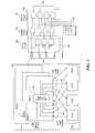
- FIG. 1is a block diagram that illustrates components of a multi-port memory device.
- FIG. 2is a flow diagram that illustrates the processing of a bank access controller of the multi-port memory device.
- FIG. 3Ais a block diagram that illustrates a bank refresh control module.
- FIG. 3Bis a state diagram that illustrates the states of the bank refresh control module of FIG. 3A .
- the multi-port memory deviceincludes multiple ports to which components of a multiprocessor system are attached, and one or more banks of memory within the multi-port memory device that are shared by each of the ports.
- a bankprovides an indication to each port that indicates whether the bank is available for use. For example, the bank may provide a bank availability hardware pin that is signaled when the bank is available to a particular port and unsignaled when the bank is unavailable. Alternatively, the bank may provide the bank availability indication through standard pins of the memory device (e.g., data pins).
- the component attached to a portwants to use a bank of memory, the component determines if the bank is available by inspecting the bank availability indication.
- the componentsends a request to reserve the bank of memory, such as through an input control pin.
- the request to reserve a bank of DRAMmay be included with a DRAM ACT command.
- the bankmodifies the bank availability indication for each of the ports. For the port that sent the reservation request, the bank availability indication continues to indicate that the bank is available. However, for each of the other ports, the bank availability indication indicates that the bank is in use, effectively reserving the bank for the exclusive use of the component that issues the bank reservation request. Then, the component that issued the bank reservation request can read and write to the memory bank.
- the componentWhen the component is done using the memory bank, the component sends a bank release command (e.g., by unsignaling the input control pin) to relinquish the reservation of the bank.
- a bank release commande.g., by unsignaling the input control pin
- the request to release the bankmay be included with a DRAM PCG command.
- the memory bankmodifies the bank availability indication to indicate that the bank of memory is once again available for use by any of the ports.
- the multi-port memory devicecan be shared by several components simultaneously with only a small amount of additional hardware to support the sharing.
- the multi-port memory deviceestablishes a priority between ports that is used when two components simultaneously attempt to reserve a bank by sending an ACT command. For example, both components may inspect the availability pin and determine that the bank is available, and both may send an ACT command attempting to reserve the bank.
- the multi-port memory devicewill grant a reservation to the port having the higher priority.
- the componentscan use the availability pin to determine if the reservation request was successful.
- the component that had the higher prioritywill have a bank availability pin set to one, while the component having the lower priority (and each of the other ports) will have a bank availability pin set to zero.
- a componentissues an ACT command optimistically testing the availability of the bank. If the bank is available, then the ACT command succeeds and the bank availability pin indicates that the component has a reservation to access the bank of memory. If the ACT command fails (e.g., because the bank is already reserved), then the bank availability pin indicates that the bank is not available, and the component can periodically poll the bank by sending additional ACT commands to determine when the bank is available. As an optimization, the component can also wait for the bank availability pin to indicate that the bank is no longer reserved before sending additional ACT commands.
- the multi-port memory deviceprovides electronic fuses for determining which components can access each bank of memory.
- An electronic fuseis a fuse that can be blown by sending an electronic signal to a device. Many electronic fuses cannot be reset once blown, making them an effective tool for preventing software tampering with hardware configuration. For example, by blowing certain electronic fuses an application may configure the multi-port memory device such that the bank availability pin always indicates availability to one port and always indicates unavailability to the other ports. Such a configuration may be performed as part of the manufacturing process or in the field after the memory device has been incorporated in a particular application. In some applications, it is desirable to ensure that some components cannot access banks of memory used by other components to enforce a form of hardware firewall between the components.
- mobile phonesoften are designed to protect the memory used by a baseband processor that communicates with the mobile phone provider's network, from erroneous behavior of a media processor, which runs an operating system that presents the user interface to the mobile phone user.
- This type of designprevents errors in the operating system software from affecting the provider's network such as could occur if invalid data were sent over the provider's network.
- the media processorcan be prevented through hardware from accessing memory banks used by the baseband processor.
- the multi-port memory deviceprovides a mode set register (MRS) that an application can use to dynamically change the configuration of the availability of a bank of memory.
- MRSmode set register
- the MRScan be set repeatedly by software to modify the configuration of the multi-port memory device over time.
- a master electronic fusecan be used to determine whether the current configuration is set by the mode set register or by other electronic fuses.
- the applicationcan blow the master electronic fuse so that the configuration of the other electronic fuses will control the configuration of the device, and software can be prevented from making additional changes to the configuration.
- the master fuseis not blown and the configuration data in the MRS controls the configuration of the device.
- FIG. 1is a block diagram that illustrates components of a multi-port memory device 100 in one embodiment.
- the multi-port memory device 100contains one or more banks of memory 110 , one or more serial ports 120 , one or more bank access controllers 130 associated with each of the banks of memory, one or more electronic fuses 140 , input control pins 145 , and output control pins 150 .
- the banks of memory 110are typically banks of dynamic random access memory (DRAM), which may vary in size and are shared by the ports 120 .
- Ports 120are serial ports that allow data to be transmitted to and received from components (not shown) that are coupled to the ports.
- the bank access controllers 130determine which ports can access which banks of memory at any particular time.
- a bank access controller 130is associated with each bank of memory 110 and handles bank access requests for that bank.
- a bank usage requeste.g., an ACT command
- the bank access controller 130 associated with the particular bank of memorydetermines how to respond to the request, and replies using the output control pins 150 with either a bank usage grant or denial.
- the bank access controller 130allows three options for bank access control: no control, control by configuration, and priority-based control.
- the no control optionmeans that access to the associated bank is not regulated by the memory device.
- the no control optionrelies on external coordination among multiple components or port masters to manage access to the bank.
- the no control optionmay be selected by asserting a bypass access control signal.
- the control by configuration optionmeans that access to the bank is limited based on a configuration of the memory device.
- Control by configurationuses either an electronic fuse or a mode register to assign bank access rights to each port. Another fuse may be used to select whether assignments occur by fuse or mode register.
- the priority-based control optionmeans that exclusive usage rights are granted to a port based on a priority established among competing ports.
- each bank access controller 130contains internal logic that determines whether a bank usage request will be granted or denied for the associated bank.
- the bank access controlincludes: 1) a priority encoder 160 that determines a priority among the ports, 2) a disable access control 170 that allows the associated bank of memory to be disabled from access, and 3) an external access control 180 that responds to the settings of configuration data (e.g., a mode register set (MRS) and/or one or more electronic fuses 140 ).
- the priority encoder 160establishes a priority among the ports such that a higher priority component that makes a simultaneous request to access a bank of memory will be granted access over a lower priority component.
- the priority encoder operationdepends on higher priority components being connected to lower numbered ports (e.g., port 0 , port 1 ) than lower priority components which are connected to higher numbered ports (e.g., port 2 , port 3 ).
- the disable access controlallows the corresponding bank to be disabled by the application of a single disable control signal applied on line 185 .
- the external access control 180allows certain ports to be prevented from accessing the corresponding bank of memory.
- the state of the external access controlis dependent on configuration data that is applied to the access control. Such configuration data may come from the settings of the MRS or one or more fuses 140 .
- the state of the MRS or fuses 140are applied to the logic forming the external access control, allowing access to the corresponding bank to be denied to one or more of the ports until the state of the MRS or fuses is changed. For example, as described herein, it may be desirable in some applications to prevent one component from accessing memory used by another component at a hardware level. This can be used to prevent software errors from causing memory corruption across components.
- FIG. 2is a flow diagram that illustrates the processing of one of the bank access controllers 130 of the multi-port memory device.
- the controllerreceives a request to access a bank of the multi-port memory device from a component attached to one of the ports.
- the controllerdetermines the priority and configuration established for the particular port. The determination may include inspecting a priority table, reading the values of one or more electronic fuses, and so forth, to determine whether the requesting port is allowed to access the bank of memory at the current time.
- decision block 230if the port is not allowed to access the bank, then the bank access controller continues at block 240 and denies the access request, else the controller continues at block 250 .
- the controllergrants the access request and the component attached to the port can begin reading and writing to the memory.
- the bank access controllerprovides an indication to components attached to other ports that the bank is reserved and not currently available. After block 260 , these steps conclude.
- the multi-port memory devicemay send a message to the component indicating that access was denied.
- the componentmay handle the message by completing any ongoing read burst and then reissuing the failed command later. For example, a component may repeatedly poll a particular bank until it is available by reissuing a command to access the bank until the command succeeds.
- the DRAM banks 110 contained in the multi-port memory device 100typically have specific timing considerations that govern the way in which the DRAM can be accessed.
- the DRAMmay have the following timing parameters:
- Row Cycle TimeThe minimum time in cycles that it takes a row to complete a full cycle. If tRC is set too short, it can cause corruption of data, and if it is set too long, it will cause a loss in performance but increased stability.
- Row to Row DelaytRRD
- tRRDRow to Row Delay
- tRFCRow Refresh Cycle
- tRFCWrite Recovery Time
- tRWThe amount of time in cycles required after a valid write operation and precharge to insure that data is written properly.
- tRTWRead to Write Delay
- tWTRWrite to Read Delay
- tREFRefresh Time
- the multi-port memory device 100must observe any timing considerations required by the DRAM to ensure a consistent memory state.
- the bank of memoryis shared among multiple components, one component using the bank may not know what another component has done with the bank. This can make it difficult, for example, to ensure that a sufficient read to write delay has elapsed or that a sufficient refresh interval has been maintained.
- componentstypically are responsible for sending an auto refresh command (REFA) that refreshes the banks of the multi-port memory device after certain types of commands.
- REFAauto refresh command
- the multi-port memory device 100employs its own automatic or local refresh scheme described herein.
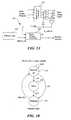
- FIG. 3Ais a block diagram that illustrates a bank refresh control module 300 .
- the multi-port memory deviceuses the bank refresh control module 300 to temporarily prevent access to memory banks during a refresh cycle (hereinafter referred to as a “local refresh”).
- the modulecomprises a refresh timer 310 coupled to a bank refresh controller 320 .
- the refresh controller 320is coupled to the DRAM memory banks, and can issue refresh signals to refresh the memory when the memory is not in use.
- the refresh timer 310periodically issues a refresh_tick signal.
- the refresh_tick signalindicates that a bank refresh must be performed, and can be generated globally for all banks in the multi-port memory device or generated locally for each bank within the device.
- the bank refresh controller 320receives the refresh_tick signal and determines whether the bank is in use by logically OR-ing the bank usage grant signals from the bank access controller 130 . If the bank is not in use the bank refresh controller 320 generates refresh signals to refresh the bank.
- the bank refresh control 320also generates a logic “1” signal, in_refresh, which is inverted and combined through a logical AND with the bank usage grant signals of the bank access controller 330 to prevent access to the bank of memory when a refresh operation is in progress. Any attempt to access the bank during a refresh operation will cause an access denied message to be sent to the requesting component, and the component will typically retry the access attempt later after which the refresh may have completed.
- the bank refresh controller 320sets the in_refresh signal to logic “0” to enable normal action of the bank access controller 130 . If the bank is in use when the bank refresh controller 320 receives the refresh_tick signal, the bank refresh controller waits for the bank to no longer be in use before completing the refresh operation.
- FIG. 3Bis a state diagram that illustrates the states of the bank refresh control module 300 of FIG. 3A .
- the refresh_tick, in_use, and in_refresh linesare not signaled and normal memory operations are permitted. If the refresh_tick line becomes signaled and the bank of memory is not in use, the state changes to the refresh state 390 . If the bank of memory is in use, the state changes to the wait state 380 to wait for the in_use line to become unsignaled when the operation using the bank of memory completes. Then, the state changes to the refresh state 390 .
- the bank refresh control modulecompletes a refresh operation. After the refresh operation is complete, designated by the passage of tRC, the state returns to the normal state 370 and components can once again perform memory operations using the bank.
- the refresh timer 310 of FIG. 3Ais replaced by a command decoder that automatically determines when a refresh is needed based on the types of commands issued to the bank.
- This schemecalled an auto refresh scheme, requires more hardware, but allows components to use the bank of memory with fewer refresh delays.
- the multi-port memory deviceis architected to reduce the time required between operations that access the DRAM.
- the column widthmay be constrained to relieve energy for bank activation.
- the multi-port memory devicemay also use separate voltage generators per bank to remove constraints such as tRRD and tFAW. Those of ordinary skill in the art will recognize that these and other designs can be used to reduce contention between multiple components sharing a bank of memory.
Landscapes
- Engineering & Computer Science (AREA)
- Microelectronics & Electronic Packaging (AREA)
- Computer Hardware Design (AREA)
- Multimedia (AREA)
- Dram (AREA)
- Memory System (AREA)
Abstract
Description
| Commands Per Clock | The amount of time in cycles between when a chip select is |
| (CPC)/Command Rate | executed and commands can be issued. |
| Row Cycle Time (tRC) | The minimum time in cycles that it takes a row to complete |
| a full cycle. If tRC is set too short, it can cause corruption | |
| of data, and if it is set too long, it will cause a loss in | |
| performance but increased stability. | |
| Row to Row Delay (tRRD) | The amount of cycles that it takes to activate the next row |
| of memory. The lower the timing, the better the | |
| performance, but low tRRD values can cause instability. | |
| Row Refresh Cycle (tRFC) | The amount of cycles it takes to refresh a row on a memory |
| bank. If tRFC is set too short, it can cause corruption of | |
| data and if it is set too long, it will cause a loss in | |
| performance, but increased stability. | |
| Write Recovery Time (tRW) | The amount of time in cycles required after a valid write |
| operation and precharge to insure that data is written | |
| properly. | |
| Read to Write Delay (tRTW) | When a write command is received, the amount of time in |
| cycles for the command to be executed. | |
| Write to Read Delay (tWTR) | The amount of time in cycles required between a valid write |
| command and the next read command. A lower tWTR | |
| offers better performance, but can cause instability. | |
| Refresh Time (tREF) | The maximum number of cycles before a memory cell |
| needs to be refreshed so that it does not lose its charge | |
| and become corrupt. | |
Claims (21)
Priority Applications (7)
| Application Number | Priority Date | Filing Date | Title |
|---|---|---|---|
| US11/952,052US8001334B2 (en) | 2007-12-06 | 2007-12-06 | Bank sharing and refresh in a shared multi-port memory device |
| KR1020107014889AKR101558482B1 (en) | 2007-12-06 | 2008-11-12 | Bank sharing and refresh in a shared multi-port memory device |
| EP08856591.6AEP2243139B1 (en) | 2007-12-06 | 2008-11-12 | Bank sharing and refresh in a shared multi-port memory device |
| JP2010536963AJP5597546B2 (en) | 2007-12-06 | 2008-11-12 | Bank sharing and refresh in shared multiport memory devices |
| CN200880119252.9ACN101884071B (en) | 2007-12-06 | 2008-11-12 | Bank sharing and refresh in a shared multi-port memory device |
| PCT/US2008/083284WO2009073331A1 (en) | 2007-12-06 | 2008-11-12 | Bank sharing and refresh in a shared multi-port memory device |
| TW097144205ATWI391949B (en) | 2007-12-06 | 2008-11-14 | Bank sharing and refresh in a shared multi-port memory device |
Applications Claiming Priority (1)
| Application Number | Priority Date | Filing Date | Title |
|---|---|---|---|
| US11/952,052US8001334B2 (en) | 2007-12-06 | 2007-12-06 | Bank sharing and refresh in a shared multi-port memory device |
Publications (2)
| Publication Number | Publication Date |
|---|---|
| US20090150621A1 US20090150621A1 (en) | 2009-06-11 |
| US8001334B2true US8001334B2 (en) | 2011-08-16 |
Family
ID=40254406
Family Applications (1)
| Application Number | Title | Priority Date | Filing Date |
|---|---|---|---|
| US11/952,052Active2030-01-25US8001334B2 (en) | 2007-12-06 | 2007-12-06 | Bank sharing and refresh in a shared multi-port memory device |
Country Status (7)
| Country | Link |
|---|---|
| US (1) | US8001334B2 (en) |
| EP (1) | EP2243139B1 (en) |
| JP (1) | JP5597546B2 (en) |
| KR (1) | KR101558482B1 (en) |
| CN (1) | CN101884071B (en) |
| TW (1) | TWI391949B (en) |
| WO (1) | WO2009073331A1 (en) |
Cited By (20)
| Publication number | Priority date | Publication date | Assignee | Title |
|---|---|---|---|---|
| US20110058440A1 (en)* | 2009-09-09 | 2011-03-10 | Fusion-Io, Inc. | Apparatus, system, and method for power reduction management in a storage device |
| US20110225369A1 (en)* | 2010-03-10 | 2011-09-15 | Park Jae-Un | Multiport data cache apparatus and method of controlling the same |
| US8527693B2 (en) | 2010-12-13 | 2013-09-03 | Fusion IO, Inc. | Apparatus, system, and method for auto-commit memory |
| US8972627B2 (en) | 2009-09-09 | 2015-03-03 | Fusion-Io, Inc. | Apparatus, system, and method for managing operations for data storage media |
| US8984216B2 (en) | 2010-09-09 | 2015-03-17 | Fusion-Io, Llc | Apparatus, system, and method for managing lifetime of a storage device |
| US9021158B2 (en) | 2009-09-09 | 2015-04-28 | SanDisk Technologies, Inc. | Program suspend/resume for memory |
| US9047178B2 (en) | 2010-12-13 | 2015-06-02 | SanDisk Technologies, Inc. | Auto-commit memory synchronization |
| US9208071B2 (en) | 2010-12-13 | 2015-12-08 | SanDisk Technologies, Inc. | Apparatus, system, and method for accessing memory |
| US9218278B2 (en) | 2010-12-13 | 2015-12-22 | SanDisk Technologies, Inc. | Auto-commit memory |
| US9223514B2 (en) | 2009-09-09 | 2015-12-29 | SanDisk Technologies, Inc. | Erase suspend/resume for memory |
| US9600184B2 (en) | 2007-12-06 | 2017-03-21 | Sandisk Technologies Llc | Apparatus, system, and method for coordinating storage requests in a multi-processor/multi-thread environment |
| US9666244B2 (en) | 2014-03-01 | 2017-05-30 | Fusion-Io, Inc. | Dividing a storage procedure |
| US9734086B2 (en) | 2006-12-06 | 2017-08-15 | Sandisk Technologies Llc | Apparatus, system, and method for a device shared between multiple independent hosts |
| US9933950B2 (en) | 2015-01-16 | 2018-04-03 | Sandisk Technologies Llc | Storage operation interrupt |
| US9940991B2 (en) | 2015-11-06 | 2018-04-10 | Samsung Electronics Co., Ltd. | Memory device and memory system performing request-based refresh, and operating method of the memory device |
| US10346345B2 (en) | 2017-05-26 | 2019-07-09 | Microsoft Technology Licensing, Llc | Core mapping |
| US10353815B2 (en) | 2017-05-26 | 2019-07-16 | Microsoft Technology Licensing, Llc | Data security for multiple banks of memory |
| US10587575B2 (en) | 2017-05-26 | 2020-03-10 | Microsoft Technology Licensing, Llc | Subsystem firewalls |
| US10817502B2 (en) | 2010-12-13 | 2020-10-27 | Sandisk Technologies Llc | Persistent memory management |
| US10817421B2 (en) | 2010-12-13 | 2020-10-27 | Sandisk Technologies Llc | Persistent data structures |
Families Citing this family (36)
| Publication number | Priority date | Publication date | Assignee | Title |
|---|---|---|---|---|
| US8489817B2 (en) | 2007-12-06 | 2013-07-16 | Fusion-Io, Inc. | Apparatus, system, and method for caching data |
| US8443134B2 (en) | 2006-12-06 | 2013-05-14 | Fusion-Io, Inc. | Apparatus, system, and method for graceful cache device degradation |
| US8706968B2 (en) | 2007-12-06 | 2014-04-22 | Fusion-Io, Inc. | Apparatus, system, and method for redundant write caching |
| US9104599B2 (en) | 2007-12-06 | 2015-08-11 | Intelligent Intellectual Property Holdings 2 Llc | Apparatus, system, and method for destaging cached data |
| KR20090013342A (en)* | 2007-08-01 | 2009-02-05 | 삼성전자주식회사 | Multi-port semiconductor memory device and refresh method accordingly |
| US8402410B2 (en)* | 2007-08-27 | 2013-03-19 | Samsung Electronics Co., Ltd. | Method and apparatus for managing configuration memory of reconfigurable hardware |
| US9519540B2 (en) | 2007-12-06 | 2016-12-13 | Sandisk Technologies Llc | Apparatus, system, and method for destaging cached data |
| WO2010123681A2 (en) | 2009-04-22 | 2010-10-28 | Rambus Inc. | Protocol for refresh between a memory controller and a memory device |
| US9104581B2 (en) | 2010-06-24 | 2015-08-11 | International Business Machines Corporation | eDRAM refresh in a high performance cache architecture |
| US8244972B2 (en) | 2010-06-24 | 2012-08-14 | International Business Machines Corporation | Optimizing EDRAM refresh rates in a high performance cache architecture |
| US8380940B2 (en)* | 2010-06-25 | 2013-02-19 | Qualcomm Incorporated | Multi-channel multi-port memory |
| KR101796116B1 (en) | 2010-10-20 | 2017-11-10 | 삼성전자 주식회사 | Semiconductor device, memory module and memory system having the same and operating method thereof |
| US9092337B2 (en) | 2011-01-31 | 2015-07-28 | Intelligent Intellectual Property Holdings 2 Llc | Apparatus, system, and method for managing eviction of data |
| WO2012116369A2 (en) | 2011-02-25 | 2012-08-30 | Fusion-Io, Inc. | Apparatus, system, and method for managing contents of a cache |
| US8943330B2 (en)* | 2011-05-10 | 2015-01-27 | Qualcomm Incorporated | Apparatus and method for hardware-based secure data processing using buffer memory address range rules |
| US9767032B2 (en) | 2012-01-12 | 2017-09-19 | Sandisk Technologies Llc | Systems and methods for cache endurance |
| US9251086B2 (en) | 2012-01-24 | 2016-02-02 | SanDisk Technologies, Inc. | Apparatus, system, and method for managing a cache |
| CN103294405B (en)* | 2012-03-02 | 2016-08-17 | 联想(北京)有限公司 | Data read-write method and electronic equipment |
| CN103309871B (en)* | 2012-03-09 | 2016-12-14 | 联想(北京)有限公司 | File read/write method and electronic equipment |
| CN103514067A (en)* | 2012-06-28 | 2014-01-15 | 鸿富锦精密工业(深圳)有限公司 | Memory bank |
| CN103530208A (en)* | 2012-07-04 | 2014-01-22 | 鸿富锦精密工业(深圳)有限公司 | Memory bank |
| JP2014067241A (en)* | 2012-09-26 | 2014-04-17 | Fujitsu Semiconductor Ltd | Semiconductor memory device and electronic device |
| US9979180B2 (en)* | 2014-10-20 | 2018-05-22 | Infineon Technologies Ag | Electronic fuse |
| US11114138B2 (en)* | 2017-09-15 | 2021-09-07 | Groq, Inc. | Data structures with multiple read ports |
| US11243880B1 (en) | 2017-09-15 | 2022-02-08 | Groq, Inc. | Processor architecture |
| US11360934B1 (en) | 2017-09-15 | 2022-06-14 | Groq, Inc. | Tensor streaming processor architecture |
| US11868804B1 (en) | 2019-11-18 | 2024-01-09 | Groq, Inc. | Processor instruction dispatch configuration |
| US11170307B1 (en) | 2017-09-21 | 2021-11-09 | Groq, Inc. | Predictive model compiler for generating a statically scheduled binary with known resource constraints |
| US12340300B1 (en) | 2018-09-14 | 2025-06-24 | Groq, Inc. | Streaming processor architecture |
| US11537687B2 (en) | 2018-11-19 | 2022-12-27 | Groq, Inc. | Spatial locality transform of matrices |
| US11216212B2 (en) | 2019-03-19 | 2022-01-04 | International Business Machines Corporation | Minimizing conflicts in multiport banked memory arrays |
| US11030128B2 (en)* | 2019-08-05 | 2021-06-08 | Cypress Semiconductor Corporation | Multi-ported nonvolatile memory device with bank allocation and related systems and methods |
| CN112783805B (en)* | 2019-11-05 | 2023-11-21 | 晶豪科技股份有限公司 | Memory chip, memory module and method for pseudo-accessing memory bank thereof |
| KR20210113859A (en)* | 2020-03-09 | 2021-09-17 | 에스케이하이닉스 주식회사 | Data Processing System and Operating Method Thereof |
| KR20220111444A (en) | 2021-02-02 | 2022-08-09 | 삼성전자주식회사 | Memory device and operating method thereof |
| WO2025174400A1 (en)* | 2024-02-16 | 2025-08-21 | Google Llc | Multi-port memory testing |
Citations (16)
| Publication number | Priority date | Publication date | Assignee | Title |
|---|---|---|---|---|
| US4745545A (en)* | 1985-06-28 | 1988-05-17 | Cray Research, Inc. | Memory reference control in a multiprocessor |
| US5463590A (en)* | 1993-03-19 | 1995-10-31 | Kabushiki Kaisha Toshiba | Multi-bank semiconductor memory device having common command detection |
| US5875470A (en)* | 1995-09-28 | 1999-02-23 | International Business Machines Corporation | Multi-port multiple-simultaneous-access DRAM chip |
| US6088760A (en) | 1997-03-07 | 2000-07-11 | Mitsubishi Semiconductor America, Inc. | Addressing system in a multi-port RAM having main and cache memories |
| US6279084B1 (en)* | 1997-10-24 | 2001-08-21 | Compaq Computer Corporation | Shadow commands to optimize sequencing of requests in a switch-based multi-processor system |
| US6298413B1 (en)* | 1998-11-19 | 2001-10-02 | Micron Technology, Inc. | Apparatus for controlling refresh of a multibank memory device |
| US6789155B2 (en)* | 2001-08-29 | 2004-09-07 | Micron Technology, Inc. | System and method for controlling multi-bank embedded DRAM |
| US20050268050A1 (en)* | 2004-02-07 | 2005-12-01 | Woon-Sik Suh | Multi-port memory device providing protection signal |
| US20060161338A1 (en)* | 2001-10-25 | 2006-07-20 | Samsung Electronics Co., Ltd. | Multi-port memory device providing protection signal |
| US7107386B1 (en)* | 2001-08-08 | 2006-09-12 | Pasternak Solutions, Llc | Memory bus arbitration using memory bank readiness |
| US20060294322A1 (en)* | 2000-12-20 | 2006-12-28 | Fujitsu Limited | Multi-port memory based on DRAM core |
| US20070022245A1 (en)* | 2005-07-25 | 2007-01-25 | Samsung Electronics Co., Ltd. | Method of controlling refresh operation in multi-port dram and a memory system using the method |
| US20070070743A1 (en) | 2005-09-29 | 2007-03-29 | Hynix Semiconductor Inc. | Multi-port semiconductor memory device |
| US20090059711A1 (en)* | 2007-08-29 | 2009-03-05 | Chi-Sung Oh | Routing access with minimized bus area in multi-port memory device |
| US20090106503A1 (en)* | 2007-10-23 | 2009-04-23 | Dong-Hyuk Lee | Method, device, and system for preventing refresh starvation in shared memory bank |
| US7596666B2 (en)* | 2005-12-22 | 2009-09-29 | Samsung Electronics Co., Ltd. | Multi-path accessible semiconductor memory device having port state signaling function |
Family Cites Families (5)
| Publication number | Priority date | Publication date | Assignee | Title |
|---|---|---|---|---|
| JP2673390B2 (en)* | 1991-03-13 | 1997-11-05 | 三菱電機株式会社 | Multi-port memory |
| JP4116801B2 (en)* | 2002-03-14 | 2008-07-09 | 富士通株式会社 | Semiconductor memory device |
| KR100689863B1 (en)* | 2005-12-22 | 2007-03-08 | 삼성전자주식회사 | Semiconductor memory device and method thereof |
| KR100735568B1 (en)* | 2006-01-23 | 2007-07-04 | 삼성전자주식회사 | Option Circuit and Method of Semiconductor Chip |
| JP4205743B2 (en)* | 2006-08-22 | 2009-01-07 | エルピーダメモリ株式会社 | Semiconductor memory device and semiconductor device |
- 2007
- 2007-12-06USUS11/952,052patent/US8001334B2/enactiveActive
- 2008
- 2008-11-12CNCN200880119252.9Apatent/CN101884071B/enactiveActive
- 2008-11-12WOPCT/US2008/083284patent/WO2009073331A1/enactiveApplication Filing
- 2008-11-12EPEP08856591.6Apatent/EP2243139B1/enactiveActive
- 2008-11-12KRKR1020107014889Apatent/KR101558482B1/enactiveActive
- 2008-11-12JPJP2010536963Apatent/JP5597546B2/enactiveActive
- 2008-11-14TWTW097144205Apatent/TWI391949B/enactive
Patent Citations (18)
| Publication number | Priority date | Publication date | Assignee | Title |
|---|---|---|---|---|
| US4745545A (en)* | 1985-06-28 | 1988-05-17 | Cray Research, Inc. | Memory reference control in a multiprocessor |
| US5463590A (en)* | 1993-03-19 | 1995-10-31 | Kabushiki Kaisha Toshiba | Multi-bank semiconductor memory device having common command detection |
| US5875470A (en)* | 1995-09-28 | 1999-02-23 | International Business Machines Corporation | Multi-port multiple-simultaneous-access DRAM chip |
| US6088760A (en) | 1997-03-07 | 2000-07-11 | Mitsubishi Semiconductor America, Inc. | Addressing system in a multi-port RAM having main and cache memories |
| US6279084B1 (en)* | 1997-10-24 | 2001-08-21 | Compaq Computer Corporation | Shadow commands to optimize sequencing of requests in a switch-based multi-processor system |
| US6298413B1 (en)* | 1998-11-19 | 2001-10-02 | Micron Technology, Inc. | Apparatus for controlling refresh of a multibank memory device |
| US20060294322A1 (en)* | 2000-12-20 | 2006-12-28 | Fujitsu Limited | Multi-port memory based on DRAM core |
| US20060271724A1 (en)* | 2001-08-08 | 2006-11-30 | Pasternak Solutions Llc | Memory bus arbitration using memory bank readiness |
| US7107386B1 (en)* | 2001-08-08 | 2006-09-12 | Pasternak Solutions, Llc | Memory bus arbitration using memory bank readiness |
| US6789155B2 (en)* | 2001-08-29 | 2004-09-07 | Micron Technology, Inc. | System and method for controlling multi-bank embedded DRAM |
| US20060161338A1 (en)* | 2001-10-25 | 2006-07-20 | Samsung Electronics Co., Ltd. | Multi-port memory device providing protection signal |
| US7539825B2 (en)* | 2001-10-25 | 2009-05-26 | Samsung Electronics Co., Ltd. | Multi-port memory device providing protection signal |
| US20050268050A1 (en)* | 2004-02-07 | 2005-12-01 | Woon-Sik Suh | Multi-port memory device providing protection signal |
| US20070022245A1 (en)* | 2005-07-25 | 2007-01-25 | Samsung Electronics Co., Ltd. | Method of controlling refresh operation in multi-port dram and a memory system using the method |
| US20070070743A1 (en) | 2005-09-29 | 2007-03-29 | Hynix Semiconductor Inc. | Multi-port semiconductor memory device |
| US7596666B2 (en)* | 2005-12-22 | 2009-09-29 | Samsung Electronics Co., Ltd. | Multi-path accessible semiconductor memory device having port state signaling function |
| US20090059711A1 (en)* | 2007-08-29 | 2009-03-05 | Chi-Sung Oh | Routing access with minimized bus area in multi-port memory device |
| US20090106503A1 (en)* | 2007-10-23 | 2009-04-23 | Dong-Hyuk Lee | Method, device, and system for preventing refresh starvation in shared memory bank |
Non-Patent Citations (2)
| Title |
|---|
| "ISR WO Mailed Feb. 4, 2009 for PCT/US2008/083284", Whole Document. |
| International Preliminary Report on Patentability for International Patent Application No. PCT/US2008/083284 mailed Jun. 8, 2010. |
Cited By (34)
| Publication number | Priority date | Publication date | Assignee | Title |
|---|---|---|---|---|
| US11847066B2 (en) | 2006-12-06 | 2023-12-19 | Unification Technologies Llc | Apparatus, system, and method for managing commands of solid-state storage using bank interleave |
| US9734086B2 (en) | 2006-12-06 | 2017-08-15 | Sandisk Technologies Llc | Apparatus, system, and method for a device shared between multiple independent hosts |
| US11573909B2 (en) | 2006-12-06 | 2023-02-07 | Unification Technologies Llc | Apparatus, system, and method for managing commands of solid-state storage using bank interleave |
| US11640359B2 (en) | 2006-12-06 | 2023-05-02 | Unification Technologies Llc | Systems and methods for identifying storage resources that are not in use |
| US11960412B2 (en) | 2006-12-06 | 2024-04-16 | Unification Technologies Llc | Systems and methods for identifying storage resources that are not in use |
| US9600184B2 (en) | 2007-12-06 | 2017-03-21 | Sandisk Technologies Llc | Apparatus, system, and method for coordinating storage requests in a multi-processor/multi-thread environment |
| US8429436B2 (en) | 2009-09-09 | 2013-04-23 | Fusion-Io, Inc. | Apparatus, system, and method for power reduction in a storage device |
| US8972627B2 (en) | 2009-09-09 | 2015-03-03 | Fusion-Io, Inc. | Apparatus, system, and method for managing operations for data storage media |
| US20110058440A1 (en)* | 2009-09-09 | 2011-03-10 | Fusion-Io, Inc. | Apparatus, system, and method for power reduction management in a storage device |
| US9021158B2 (en) | 2009-09-09 | 2015-04-28 | SanDisk Technologies, Inc. | Program suspend/resume for memory |
| US8289801B2 (en) | 2009-09-09 | 2012-10-16 | Fusion-Io, Inc. | Apparatus, system, and method for power reduction management in a storage device |
| US9223514B2 (en) | 2009-09-09 | 2015-12-29 | SanDisk Technologies, Inc. | Erase suspend/resume for memory |
| US20110060927A1 (en)* | 2009-09-09 | 2011-03-10 | Fusion-Io, Inc. | Apparatus, system, and method for power reduction in a storage device |
| US9305610B2 (en) | 2009-09-09 | 2016-04-05 | SanDisk Technologies, Inc. | Apparatus, system, and method for power reduction management in a storage device |
| US8583873B2 (en)* | 2010-03-10 | 2013-11-12 | Samsung Electronics Co., Ltd. | Multiport data cache apparatus and method of controlling the same |
| US20110225369A1 (en)* | 2010-03-10 | 2011-09-15 | Park Jae-Un | Multiport data cache apparatus and method of controlling the same |
| US8984216B2 (en) | 2010-09-09 | 2015-03-17 | Fusion-Io, Llc | Apparatus, system, and method for managing lifetime of a storage device |
| US9047178B2 (en) | 2010-12-13 | 2015-06-02 | SanDisk Technologies, Inc. | Auto-commit memory synchronization |
| US9223662B2 (en) | 2010-12-13 | 2015-12-29 | SanDisk Technologies, Inc. | Preserving data of a volatile memory |
| US9767017B2 (en) | 2010-12-13 | 2017-09-19 | Sandisk Technologies Llc | Memory device with volatile and non-volatile media |
| US9772938B2 (en) | 2010-12-13 | 2017-09-26 | Sandisk Technologies Llc | Auto-commit memory metadata and resetting the metadata by writing to special address in free space of page storing the metadata |
| US8527693B2 (en) | 2010-12-13 | 2013-09-03 | Fusion IO, Inc. | Apparatus, system, and method for auto-commit memory |
| US9218278B2 (en) | 2010-12-13 | 2015-12-22 | SanDisk Technologies, Inc. | Auto-commit memory |
| US10817502B2 (en) | 2010-12-13 | 2020-10-27 | Sandisk Technologies Llc | Persistent memory management |
| US10817421B2 (en) | 2010-12-13 | 2020-10-27 | Sandisk Technologies Llc | Persistent data structures |
| US9208071B2 (en) | 2010-12-13 | 2015-12-08 | SanDisk Technologies, Inc. | Apparatus, system, and method for accessing memory |
| US9666244B2 (en) | 2014-03-01 | 2017-05-30 | Fusion-Io, Inc. | Dividing a storage procedure |
| US9933950B2 (en) | 2015-01-16 | 2018-04-03 | Sandisk Technologies Llc | Storage operation interrupt |
| US9940991B2 (en) | 2015-11-06 | 2018-04-10 | Samsung Electronics Co., Ltd. | Memory device and memory system performing request-based refresh, and operating method of the memory device |
| US10127974B2 (en) | 2015-11-06 | 2018-11-13 | Samsung Electronics Co., Ltd. | Memory device and memory system performing request-based refresh, and operating method of the memory device |
| US10353815B2 (en) | 2017-05-26 | 2019-07-16 | Microsoft Technology Licensing, Llc | Data security for multiple banks of memory |
| US11444918B2 (en) | 2017-05-26 | 2022-09-13 | Microsoft Technology Licensing, Llc | Subsystem firewalls |
| US10587575B2 (en) | 2017-05-26 | 2020-03-10 | Microsoft Technology Licensing, Llc | Subsystem firewalls |
| US10346345B2 (en) | 2017-05-26 | 2019-07-09 | Microsoft Technology Licensing, Llc | Core mapping |
Also Published As
| Publication number | Publication date |
|---|---|
| KR20100095459A (en) | 2010-08-30 |
| WO2009073331A1 (en) | 2009-06-11 |
| TW200943317A (en) | 2009-10-16 |
| JP2011507071A (en) | 2011-03-03 |
| EP2243139B1 (en) | 2016-02-10 |
| KR101558482B1 (en) | 2015-10-07 |
| US20090150621A1 (en) | 2009-06-11 |
| JP5597546B2 (en) | 2014-10-01 |
| EP2243139A1 (en) | 2010-10-27 |
| CN101884071A (en) | 2010-11-10 |
| TWI391949B (en) | 2013-04-01 |
| CN101884071B (en) | 2014-08-06 |
Similar Documents
| Publication | Publication Date | Title |
|---|---|---|
| US8001334B2 (en) | Bank sharing and refresh in a shared multi-port memory device | |
| US6330645B1 (en) | Multi-stream coherent memory controller apparatus and method | |
| JP5079279B2 (en) | Refresh control method in multi-port DRAM and multi-port memory system using the method | |
| KR100816053B1 (en) | Memory devices, memory systems, and dual-port memory devices with self-copy capability | |
| US8711652B2 (en) | Arbitration for memory device with commands | |
| KR20160067089A (en) | Data processor with memory controller for high reliability operation and method | |
| CN107257964B (en) | DRAM circuit, computer system and method for accessing DRAM circuit | |
| US11995008B2 (en) | Memory controller with hybrid DRAM/persistent memory channel arbitration | |
| JP4560498B2 (en) | Arbitration scheme for shared memory devices | |
| KR101110550B1 (en) | A shared memory approach for processor units, multiprocessor systems, and multiprocessor systems | |
| US20050182908A1 (en) | Method and apparatus of interleaving memory bank in multi-layer bus system | |
| JP2010129029A (en) | Memory access control apparatus and memory access control method | |
| JP3962850B2 (en) | Control device for SDRAM | |
| JPH04143993A (en) | Dram controller | |
| KR20070113493A (en) | Multi-port memory device having access right register logic and control method thereof | |
| KR20070116497A (en) | Multi-port memory device and method of controlling access rights thereof | |
| KR100453118B1 (en) | Microprocessor and microprocessor systems | |
| JP2003132012A (en) | System for bus control and method therefor | |
| JPS63191398A (en) | Information processor | |
| US20070260803A1 (en) | Data processing system and method | |
| JPH08212170A (en) | Memory control device and method thereof | |
| JPH086841A (en) | Memory control device |
Legal Events
| Date | Code | Title | Description |
|---|---|---|---|
| AS | Assignment | Owner name:SILICON IMAGE, INC., CALIFORNIA Free format text:ASSIGNMENT OF ASSIGNORS INTEREST;ASSIGNOR:LEE, DONGYUN;REEL/FRAME:020214/0367 Effective date:20071003 | |
| FEPP | Fee payment procedure | Free format text:PAYOR NUMBER ASSIGNED (ORIGINAL EVENT CODE: ASPN); ENTITY STATUS OF PATENT OWNER: LARGE ENTITY | |
| STCF | Information on status: patent grant | Free format text:PATENTED CASE | |
| FPAY | Fee payment | Year of fee payment:4 | |
| AS | Assignment | Owner name:JEFFERIES FINANCE LLC, NEW YORK Free format text:SECURITY INTEREST;ASSIGNORS:LATTICE SEMICONDUCTOR CORPORATION;SIBEAM, INC.;SILICON IMAGE, INC.;AND OTHERS;REEL/FRAME:035226/0147 Effective date:20150310 | |
| AS | Assignment | Owner name:LATTICE SEMICONDUCTOR CORPORATION, OREGON Free format text:MERGER;ASSIGNOR:SILICON IMAGE, INC.;REEL/FRAME:036419/0792 Effective date:20150513 | |
| AS | Assignment | Owner name:LATTICE SEMICONDUCTOR CORPORATION, OREGON Free format text:RELEASE BY SECURED PARTY;ASSIGNOR:JEFFERIES FINANCE LLC;REEL/FRAME:036905/0327 Effective date:20151028 | |
| MAFP | Maintenance fee payment | Free format text:PAYMENT OF MAINTENANCE FEE, 8TH YEAR, LARGE ENTITY (ORIGINAL EVENT CODE: M1552); ENTITY STATUS OF PATENT OWNER: LARGE ENTITY Year of fee payment:8 | |
| AS | Assignment | Owner name:SILICON IMAGE, INC., OREGON Free format text:RELEASE BY SECURED PARTY;ASSIGNOR:JEFFERIES FINANCE LLC;REEL/FRAME:049827/0326 Effective date:20190517 Owner name:DVDO, INC., OREGON Free format text:RELEASE BY SECURED PARTY;ASSIGNOR:JEFFERIES FINANCE LLC;REEL/FRAME:049827/0326 Effective date:20190517 Owner name:LATTICE SEMICONDUCTOR CORPORATION, OREGON Free format text:RELEASE BY SECURED PARTY;ASSIGNOR:JEFFERIES FINANCE LLC;REEL/FRAME:049827/0326 Effective date:20190517 Owner name:SIBEAM, INC., OREGON Free format text:RELEASE BY SECURED PARTY;ASSIGNOR:JEFFERIES FINANCE LLC;REEL/FRAME:049827/0326 Effective date:20190517 Owner name:WELLS FARGO BANK, NATIONAL ASSOCIATION, AS ADMINIS Free format text:SECURITY INTEREST;ASSIGNOR:LATTICE SEMICONDUCTOR CORPORATION;REEL/FRAME:049980/0786 Effective date:20190517 Owner name:WELLS FARGO BANK, NATIONAL ASSOCIATION, AS ADMINISTRATIVE AGENT, COLORADO Free format text:SECURITY INTEREST;ASSIGNOR:LATTICE SEMICONDUCTOR CORPORATION;REEL/FRAME:049980/0786 Effective date:20190517 | |
| MAFP | Maintenance fee payment | Free format text:PAYMENT OF MAINTENANCE FEE, 12TH YEAR, LARGE ENTITY (ORIGINAL EVENT CODE: M1553); ENTITY STATUS OF PATENT OWNER: LARGE ENTITY Year of fee payment:12 |