US8000737B2 - Methods and apparatuses for adaptively controlling antenna parameters to enhance efficiency and maintain antenna size compactness - Google Patents
Methods and apparatuses for adaptively controlling antenna parameters to enhance efficiency and maintain antenna size compactnessDownload PDFInfo
- Publication number
- US8000737B2 US8000737B2US11/623,307US62330707AUS8000737B2US 8000737 B2US8000737 B2US 8000737B2US 62330707 AUS62330707 AUS 62330707AUS 8000737 B2US8000737 B2US 8000737B2
- Authority
- US
- United States
- Prior art keywords
- antenna
- impedance
- power
- signal
- band
- Prior art date
- Legal status (The legal status is an assumption and is not a legal conclusion. Google has not performed a legal analysis and makes no representation as to the accuracy of the status listed.)
- Expired - Fee Related, expires
Links
Images


Classifications
- H—ELECTRICITY
- H01—ELECTRIC ELEMENTS
- H01Q—ANTENNAS, i.e. RADIO AERIALS
- H01Q1/00—Details of, or arrangements associated with, antennas
- H01Q1/50—Structural association of antennas with earthing switches, lead-in devices or lightning protectors
- H—ELECTRICITY
- H01—ELECTRIC ELEMENTS
- H01Q—ANTENNAS, i.e. RADIO AERIALS
- H01Q1/00—Details of, or arrangements associated with, antennas
- H01Q1/12—Supports; Mounting means
- H01Q1/22—Supports; Mounting means by structural association with other equipment or articles
- H01Q1/24—Supports; Mounting means by structural association with other equipment or articles with receiving set
- H01Q1/241—Supports; Mounting means by structural association with other equipment or articles with receiving set used in mobile communications, e.g. GSM
- H01Q1/242—Supports; Mounting means by structural association with other equipment or articles with receiving set used in mobile communications, e.g. GSM specially adapted for hand-held use
- H01Q1/243—Supports; Mounting means by structural association with other equipment or articles with receiving set used in mobile communications, e.g. GSM specially adapted for hand-held use with built-in antennas
- H—ELECTRICITY
- H01—ELECTRIC ELEMENTS
- H01Q—ANTENNAS, i.e. RADIO AERIALS
- H01Q9/00—Electrically-short antennas having dimensions not more than twice the operating wavelength and consisting of conductive active radiating elements
- H01Q9/04—Resonant antennas
- H01Q9/0407—Substantially flat resonant element parallel to ground plane, e.g. patch antenna
- H01Q9/0421—Substantially flat resonant element parallel to ground plane, e.g. patch antenna with a shorting wall or a shorting pin at one end of the element
- H—ELECTRICITY
- H01—ELECTRIC ELEMENTS
- H01Q—ANTENNAS, i.e. RADIO AERIALS
- H01Q9/00—Electrically-short antennas having dimensions not more than twice the operating wavelength and consisting of conductive active radiating elements
- H01Q9/04—Resonant antennas
- H01Q9/0407—Substantially flat resonant element parallel to ground plane, e.g. patch antenna
- H01Q9/0442—Substantially flat resonant element parallel to ground plane, e.g. patch antenna with particular tuning means
- H—ELECTRICITY
- H01—ELECTRIC ELEMENTS
- H01Q—ANTENNAS, i.e. RADIO AERIALS
- H01Q9/00—Electrically-short antennas having dimensions not more than twice the operating wavelength and consisting of conductive active radiating elements
- H01Q9/04—Resonant antennas
- H01Q9/0407—Substantially flat resonant element parallel to ground plane, e.g. patch antenna
- H01Q9/045—Substantially flat resonant element parallel to ground plane, e.g. patch antenna with particular feeding means
- Y—GENERAL TAGGING OF NEW TECHNOLOGICAL DEVELOPMENTS; GENERAL TAGGING OF CROSS-SECTIONAL TECHNOLOGIES SPANNING OVER SEVERAL SECTIONS OF THE IPC; TECHNICAL SUBJECTS COVERED BY FORMER USPC CROSS-REFERENCE ART COLLECTIONS [XRACs] AND DIGESTS
- Y10—TECHNICAL SUBJECTS COVERED BY FORMER USPC
- Y10T—TECHNICAL SUBJECTS COVERED BY FORMER US CLASSIFICATION
- Y10T29/00—Metal working
- Y10T29/49—Method of mechanical manufacture
- Y10T29/49002—Electrical device making
- Y10T29/49016—Antenna or wave energy "plumbing" making
Definitions
- the present inventionis related generally to antennas for wireless communications devices and specifically to methods and apparatuses for adaptively controlling antenna parameters to improve performance of the communications device.
- antenna performanceis dependent on the size, shape and material composition of the antenna elements, the interaction between elements and the relationship between certain antenna physical parameters (e.g., length for a linear antenna and diameter for a loop antenna) and the wavelength of the signal received or transmitted by the antenna. These physical and electrical characteristics determine several antenna operational parameters, including input impedance, gain, directivity, signal polarization, resonant frequency, bandwidth and radiation pattern. Since the antenna is an integral element of a signal receive and transmit path of a communications device, antenna performance directly affects device performance.
- an operable antennashould have a minimum physical antenna dimension on the order of a half wavelength (or a multiple thereof) of the operating frequency to limit energy dissipated in resistive losses and maximize transmitted or received energy. Due to the effect of a ground plane image, a quarter wavelength antenna (or odd integer multiples thereof) operative above a ground plane exhibits properties similar to a half wavelength antenna. Communications device product designers prefer an efficient antenna that is capable of wide bandwidth and/or multiple frequency band operation, electrically matched (e.g., impedance matching) to the transmitting and receiving components of the communications system, and operable in multiple modes (e.g., selectable signal polarizatons and selectable radiation patterns).
- electrically matchede.g., impedance matching
- the half-wavelength dipole antennais commonly used in many applications.
- the radiation patternis the familiar donut shape with most of the energy radiated uniformly in the azimuth direction and little radiation in the elevation direction.
- Frequency bands of interest for certain communications devicesare 1710 to 1990 MHz and 2110 to 2200 MHz.
- a half-wavelength dipole antennais approximately 3.11 inches long at 1900 MHz, 3.45 inches long at 1710 MHz, and 2.68 inches long at 2200 MHz.
- the typical gainis about 2.15 dBi.
- the quarter-wavelength monopole antenna disposed above a ground planeis derived from the half-wavelength dipole.
- the physical antenna lengthis a quarter-wavelength, but interaction of the electromagnetic energy with the ground plane (creating an image antenna) causes the antenna to exhibit half-wvavelength dipole performance.
- the radiation pattern for a monopole antenna above a ground planeis similar to the half-wavelength dipole pattern, with a typical gain of approximately 2 dBi.
- the common free space (i.e., not above ground plane) loop antenna(with a diameter of approximately one-third the wavelength of the transmitted or received frequency) also displays the familiar donut radiation pattern along the radial axis, with a gain of approximately 3.1 dBi. At 1900 MHz, this antenna has a diameter of about 2 inches.
- the typical loop antenna input impedanceis 50 ohms, providing good matching characteristics to the standard 50 ohm transmission line.
- the well-known patch antennaprovides directional hemispherical coverage with a gain of approximately 4.7 dBi. Although small compared to a quarter or half wavelength antenna, the patch antenna has a relatively narrow bandwidth. The small size is only attributable to the velocity of propagation associated with the dielectric material used between the plates of the patch antenna.
- antennasare typically constructed so that the antenna length is on the order of a quarter wavelength of the radiating frequency and the antenna is operated over a ground plane, or the antenna length is a half wavelength without employing a ground plane.
- Half and quarter wavelength antennaslimit energy dissipated in resistive losses and maximize the transmitted energy. But as the operational frequency increases/decreases, the operational wavelength decreases/increases and the antenna element dimensions proportionally decrease/increase.
- the dimensions of the quarter wavelength and half wavelength antennaproportionally increase.
- the resulting larger antennaeven at a quarter wavelength, may not be suitable for use with certain communications devices, especially portable and personal communications devices intended to be cared by a user. Since these antennas tend to be larger than the communications device, they are typically mounted with a portion of the antenna protruding from the communications device and thus are susceptible to breakage.
- Smaller packaging of state-of-the-art communications devicesdoes not provide sufficient space for the conventional quarter and half wavelength antenna elements.
- Physically smaller antennas operable in the frequency bands of interesti.e., exhibiting multiple resonant frequencies and/or wide bandwidth to cover all operating frequencies of the communications device
- providing the other desired antenna-operating propertiesare especially sought after.
- gainis limited by the known relationship between the antenna operating frequency and the effective antenna electrical length (expressed in wavelengths). That is, the antenna gain is constant for all quarter wavelength antennas of a specific geometry i.e., at that operating frequency where the effective antenna length is a quarter of a wavelength of the operating frequency.
- a slow-wave structureis defined as one in which the phase velocity of the traveling wave is less than the free space velocity of light.
- the frequencydoes not change during propagation through a slow wave structure, if the wave travels slower (i.e., the phase velocity is lower) than the speed of light, the wavelength within the structure is lower than the free space wavelength.
- the slow-wave structurede-couples the conventional relationship between physical length, resonant frequency and wavelength.
- the effective electrical length of these structuresis greater than the effective electrical length of a structure propagating a wave at the speed of light.
- the resulting resonant frequency for the slow-wave structureis correspondingly increased.
- two structuresare to operate at the same resonant frequency, as a half-wave dipole, for instance, then the structure propagating a slow wave will be physically smaller than the structure propagating a wave at the speed of light.
- Such slow wave structurescan be used as antenna elements or as antenna radiating structures.
- the known Chu-Harrington relationshiprelates the size and bandwidth of an antenna. Generally, as the size decreases the antenna bandwidth also decreases. But to the contrary, as the capabilities of handset communications devices expand to provide for higher data rates and the reception of bandwidth intensive information (e.g., strewing video), the antenna bandwidth must be increased.
- bandwidth intensive informatione.g., strewing video
- the teachings of the present inventionare intended to overcome one or more of these disadvantages and thereby improve operation of the communications device.
- the inventioncomprises a communications apparatus further comprising a first antenna, a first serial configuration of a first power amplifier and a first matching network, a second serial configuration of a second power amplifier and a second matching network, a switching element for switchably selecting the first or the second serial configuration for supplying a signal to the first antenna, the first and the second power amplifiers supplying a respective first signal of a first power and a second signal of a second power different than the first power to the first antenna for transmitting and the first and the second matching networks presenting respective first and second impedances to the respective first and second power amplifiers, the first and the second impedances responsive respectively to a power-related parameter of the first and the second signals.
- the inventioncomprises a communications apparatus further comprising a transmitting antenna, a receiving antenna, a first serial configuration of a first power amplifier and a first matching network for producing a first signal, the first power amplifier operating in a first frequency band, a second serial configuration of a second power amplifier and a second matching network for producing a second signal the second power amplifier operating in a second frequency band, a first switching element for switchably supplying the first signal or the second signal to the transmitting antenna, a first receiver, a second receiver and a second switching element for switchably directing a signal received at the receiving antenna to the first receiver or the second receiver.
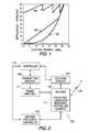
- FIG. 1is a graph illustrating power amplifier efficiency as a function of power amplifier output power
- FIGS. 2 and 3are block diagrams of communications devices according to the teachings of the present invention.
- FIGS. 4 and 5are schematic diagrams of two embodiments of components of a communications device according to the teachings of the present invention.
- FIG. 6is a perspective view and FIG. 7 is a cross-sectional view of a handset communications device.
- FIG. 8is a schematic illustration of an antenna according to one embodiment of the present invention.
- FIG. 9is a schematic illustration of parasitic capacitances of the antenna of FIG. 7 .
- FIG. 10is a schematic illustration of an antenna according to another embodiment of the present invention.
- FIG. 11-18are block diagram illustrations of apparatuses for controlling one or more antennas according to the teachings of the present invention.
- FIGS. 19-21are block diagram illustrations of various antenna control techniques according to the teachings of the present invention.
- FIG. 22is a block diagram illustration of a communications device comprising a controllable high band and low band antenna.
- FIG. 23is a perspective view of a front end module constructed according to the teachings of the present invention.
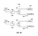
- FIG. 24is a schematic illustration of an antenna having feed points at spaced apart terminal ends according to the teachings of the present invention.
- FIG. 25is a block diagram illustration of a transmit signal path according to the teachings of the present invention.
- FIG. 26is a block diagram of an antenna system and associated components for receiving and transmitting a communications signal.
- FIGS. 27-30are block diagrams of various communications apparatuses for sending and receiving radio frequency signals according to different embodiments of the present inventions.
- FIG. 31illustrates a communications apparatus in modular form for sending and receiving radio frequency signals.
- FIGS. 32-35are block diagrams of communications apparatuses for sending and receiving radio frequency signals according to different embodiments of the present invention.
- Antenna tuning control techniquesare known in the art to provide mule-band antenna performance for a multi-band communications device.
- the present inventionteaches antenna control methods and apparatuses that overcome sub-optimal antenna impedance (introduced by the antenna tuning process) and frequency detuning effects that impair performance of the communications device.
- an antennais tuned (by controlling its effective electrical length) to a desired resonant frequency to obviate resonance detuning caused by the operating environment of the antenna. Retuning the antenna improves the antenna's performance and thus improves performance of the communications device.
- the transmitting power amplifier (PA) of a communications deviceis designed to provide a controllable output power to its load (i.e., the antenna) and to present a desired output impedance (typically 50 ohms including any impedance transformation elements).
- the output power range for which the power amplifier is designeddepends on the operating environment and the signal protocols employed by the device.
- the output poweris controlled by device components to permit effective communications with a receiving device. For example, an output power of a cellular handset PA is controlled to communicate effectively with a cellular base station as the handset moves about the base station coverage area.
- the PA efficiencychanges as the power supplied by the PA to a fixed load impedance (i.e., a fixed antenna impedance) changes. Further, the PA output power, and thus the PA efficiency, varies responsive to changes in the load impedance (the antenna impedance). It is known that although the antenna is designed to present a nominal 50 ohm impedance, in fact the impedance varies with signal frequency. For example, the antenna impedance changes when the signal frequency shifts from the antenna resonant frequency that is near the center of the antenna's operating frequency band to a signal frequency near a band edge. Since the antenna impedance changes with signal frequency, it is impossible to substantially exactly match the PA output impedance to the antenna impedance over the operating frequency band.
- the best that can be expectedis to establish a PA output impedance at the conventional 50 ohms, design the antenna for a 50 ohm impedance at the resonant frequency and recognize that inefficiencies are introduced into the system when the signal frequency differs from the resonant frequency.
- the PA efficiencymay decline as the PA output power changes and as the signal frequency changes. Reduced output power efficiency requires more battery power and thus reduces battery life.
- the antenna impedance(the PA load impedance) is controlled to present an impedance to the PA that improves a power added efficiency PAE) of the power amplifier at a commanded PA radio frequency (RF) output power. That is, the antenna impedance is controlled as a function of the PA output power. Controlling the load impedance to present a desired impedance value from a range of impedance values permits the PA output voltage and current (which determine the PA output power) to range over values that can be supplied by the PA power supply, improving the efficiency at any commanded power level. Since many communications devices operate on battery power, improving the efficiency extends “talk time” (for a specific battery size) between battery recharges. Also, controlling the antenna goad) impedance overcomes the effects of naturally occurring antenna impedance variations as the signal frequency changes.
- Yet another embodiment of the present inventioncontrols both the antenna resonant frequency and impedance to obtain the combined advantages of both techniques.
- this impedance control technique of the present inventiondiffers from the prior art impedance matching techniques of a complex conjugate match (i.e., an output impedance of a first component is a complex conjugate of an input impedance of a second component to which it is connected).
- These prior art techniquesare intended to maximize power transfer from the first component to the second component at one specific frequency, since the impedance value is frequency dependent.
- PA efficiencypower added efficiency
- PAEpower added efficiency
- Additional measures of PA efficiencycan be found at page 63 of the reference entitled “Microwave Circuit Design Using Linear Techniques and Nonlinear Techniques,” by Vendelin, Pavio and Rohde.
- the PA output impedanceis a few ohms (3 ⁇ for a common PA topology), and must be transformed (by an impedance matching circuit interposed between the PA and the amplifier) to the input impedance of the antenna, nominally 50 ⁇ .
- the reactive network required to make the transformationhas a relatively narrow bandwidth. Since this specific impedance transformation is not required according to the present invention, the bandwidth-narrowing effects of the narrow bandwidth transformation components are reduced.
- FIG. 1illustrates a graph of power amplifier PAE as a function of power amplifier output power (in dBm) for a fixed load impedance.
- the power amplifier PAEis about 50% (the theoretical maximum efficiency for a power amplifier operating in a class A mode).
- a curve 96depicts this PAE reduction when the PA has a fixed DC bins and supplies a signal to a fixed-impedance, such as a fixed 50 ohm antenna load impedance.
- a low PAEis not desired as the PA does not utilize the available power supply voltage to drive the load.
- a curve 98depicts the improved PAE attainable for a PA augmented with a DC-DC converter, i.e., to control the DC bias voltage supplied to the PA as the power output decreases.
- a DC-to-DC converter responsive to a fixed DC supply voltagegenerates a controllable DC voltage for biasing the PA responsive to the PA power output.
- This techniqueincreases the PAE as indicated by the curve 98 depicting a higher PAE than the curve 96 . But this approach requires additional components and adds complexity to the PA and the communications device with which it operates.
- GSM handsetsoperate at an average output power of about 18 dim, where the PAE is typically less than 25% according to prior art impedance matching techniques as illustrated in FIG. 1 .
- the present inventionprovides dynamic and adaptive control of the PA load impedance (i.e., the antenna impedance) responsive to the power output level of the PA.
- the antenna impedanceis adjusted, according to techniques described below, to improves the PA load impedance (the antenna impedance) responsive to the PA output power level as the PAE falls during operation of the communications device.
- Control of the PA according to the present inventionis intended to permit the PA to use all available power supply voltage/current to amplify the input signal (less any voltage that would cause the PA to saturate and clip the input signal) and extend battery life and talk-time for those communications devices operating on battery power.
- Other parameters related to the output power of the PAcan be used to control the antenna impedance, including the peak DC current in the PA output signal.
- the present inventionadjusts the antenna impedance (antenna terminal impedance) in discrete steps between a first PAE level of 40% and a second PAE of about 50%, responsive to the commanded output power. As the PAE falls to about 40%, the antenna impedance (the load impedance to the PA) is adjusted to rise the PA PAE back to about 50%.
- the present inventiontherefore provides a better PAE than offered by the prior art techniques. Control of the PA load impedance according to the teachings of the present invention can be accomplished in discrete impedance value steps, as indicated in FIG. 1 , or substantially continuously over a range of allowable and attainable impedance values.
- the PAE values depicted in FIG. 1are merely exemplary, as it is known that the actual PAE and the theoretical maximum possible PAE are determined by many factors, including the communications protocol and the power amplifier design. Also, the PA output power may be limited by the available current and voltage supplied by the power supply. As illustrated in FIG. 1 , the PAE is improved at power levels from about 0 to about 30 dBm, although the technique can be applied generally to PA's operating at any power level. Also, the PA PAE can be improved continuously, rather than discretely as depicted, by continuously modifying the antenna impedance in response to PA output power level changes. In one embodiment of the invention, the impedance control is accomplished by modifying antenna structural features as described elsewhere herein.
- Certain communications devicescomprise an impedance conversion element between the PA and the antenna.
- an impedance presented to the PA by the impedance conversion elementis controlled to control the PA efficiency.
- FIG. 2illustrates a communications device 103 comprising an antenna 105 for receiving and transmitting information signals over a radio frequency link 106 .
- the communications device 103comprises a cellular telephone handset. Signals received by the antenna 105 are processed by receiving circuits 107 to extract information contained therein. Information signals for transmitting by the antenna 105 are produced in the transmitting circuits 109 and supplied to the antenna 105 , via a power amplifier 111 , for transmitting over the radio frequency link 106 .
- a controller 110controls the receiving and transmitting circuits 107 / 109 .
- An antenna processor/controller 113(e.g., an antenna controller) is responsive to a signal supplied by the controller 110 (or alternatively is responsive to the transmitting circuits 109 or the power amplifier 111 ) that indicates operational parameters of the communications device 103 . Responsive to this signal, the processor/controller 113 develops a control signal for controlling frequency tuning and/or impedance controlling elements 117 . For example, the processor/controller 113 is responsive to the signal indicating the PA output power or the operating frequency of the communications device 103 . Responsive thereto, the processor/controller 113 effects a change to the antenna to change the antenna impedance and/or the antenna resonant frequency.
- the processor/controller 113selects a location of a feed point and/or a ground point on the antenna structure to modify the antenna's impedance and/or changes the antenna's effective electrical length by controlling radiating segments to effectively lengthen or shorten the antenna's radiating structure. Responsive to the change in antenna impedance and/or resonant frequency, the PAE improves and/or operation of the communications device improves.
- the processor/controller 113switches in or connects one or more of the impedance elements to the antenna 105 to change the antenna impedance as presented to the PA, improving the PA PAE at the commanded PA RF power output.
- insertion of a capacitor of a first value into the antenna circuitimproves the PA PAE for operation in the PCS frequency band and insertion of a capacitor of a second value improves the PAE for operation in the DCS frequency band.
- the appropriate capacitoris inserted into the antenna circuit responsive to a signal indicating the operational band of the communications device 103 that is supplied to the antenna processor/controller 113 .
- the processor/controller 113modifies (e.g., by switching antenna elements and related circuits in and/or out of the antenna circuit, moving an antenna ground point relative to its feed point or moving the feed point relative to the ground point) one or more antenna physical characteristics (e.g., effective electrical length, feed point location, ground point location) to modify the antenna resonant frequency (and/or the antenna terminal impedance) and thereby improve performance of the communications device 103 for the current operating frequency band.
- antenna physical characteristicse.g., effective electrical length, feed point location, ground point location
- One technique for controlling the antenna resonant frequencyinserts a capacitor in series with the antenna radiating structure, resulting in an appreciable resonant frequency change while only slightly changing the antenna impedance.
- a capacitor placed in parallel with the antenna radiating structurecan also change the resonant frequency, but may cause a greater change in the antenna impedance.
- the antenna resonant frequencyis modified under control of the processor/controller 113 by inserting (switching in) or deleting (switching out) conductive elements of different lengths from the antenna radiating structure.
- the control signalthus modifies the antenna effective electrical length.
- meanderline elements having different effective electrical lengthscan be switched in or out of the antenna 105 to alter the resonant frequency. Such components for effecting this resonant frequency tuning are described further below.
- the frequency tuning and/or impedance controlling elements 117 of FIG. 2can comprise elements associated with the antenna 105 or, as illustrated in FIG. 3 , can comprise impedance controlling elements 119 separate from the antenna 105 and interposed between the PA 111 and the antenna 105 . References herein to the element 117 includes the element 119 .
- Various operating parameters of the communications device 103 and its componentscan be determined and responsive thereto a control signal supplied to the frequency tuning and/or impedance controlling elements 117 .
- Such parametersinclude, but are not limited to, the PA RF output power, the operating frequency of the communications device and the VSWR on the PA/antenna signal path.
- the power amplifier in the cellular handsetis an element of a closed loop control system with a base station transceiver.
- the handset RF poweris set to a default value (probably near a maximum output power) and an operating frequency is selected.
- a signalis transmitted on a control channel to the base station requesting a frequency or time slot assignment.
- the base stationresponds with an assigned frequency and transmit power for the handset.
- the antenna impedanceis adjusted to a desired value responsive to the commanded transmit power and the antenna is tuned to the proper resonant frequency.
- the base station transceivermay command the handset to reduce or increase its output power and/or change to transmitting or receiving on a difference frequency, according to an operating scenario of the communication system and the handset.
- the new commanded power outputis employed to again adjust the antenna impedance and/or the antenna resonant frequency.
- the base station power commandcontrols the PA to change the power level of the transmitted signal and also controls the antenna impedance (the PA load impedance) to present an impedance that improves the PAE.
- the impedanceis controlled to increase the PA PAE to the maximum PAE of 50%.
- the PAEis increased without changing the PA DC bias voltage/current, although the techniques described do not prevent the use of bias control or multiple stage switched power amplifiers stages as currently known in the art.
- the VSWR(or the forward power) can be measured and a control signal derived therefrom for controlling the impedance of the antenna to improve the PAE.
- the processor/controller 113adjusts the antenna resonant frequency as described above, it may then be possible to reduce the PA output power as the signal strength or the signal-to-noise ratio at the receiving device may increase responsive to the resonant frequency change, allowing the power reduction without impairing signal quality at the receiving end.
- the antenna resonant frequency adjustmentmay also change the antenna terminal impedance, in turn affecting the power amplifier PAE.
- the resonant frequency adjustmentcan initiate an antenna terminal impedance adjustment (either directly by modifying antenna structural features or through an intermediate impedance conversion element) to improve the PAE.
- the antenna parametersare manually adjustable by the user by operation of a discretely adjustable or a continuously adjustable switching element or control component that controls the frequency tuning and impedance controlling elements 117 to change the antenna's resonant length or the antenna impedance to improve the PA PAE and overall efficiency of the communications device.
- a discretely adjustable or a continuously adjustable switching element or control componentthat controls the frequency tuning and impedance controlling elements 117 to change the antenna's resonant length or the antenna impedance to improve the PA PAE and overall efficiency of the communications device.
- Such an embodimentmay also include the processor/controller 113 for automatically adjusting the frequency tuning and impedance controlling elements 117 .
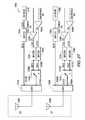
- FIG. 4illustrates an antenna 120 comprising a conductive element 124 disposed over a ground plane 128 .
- Switching elements 130 , 132 , 134 and 136switchably connect feed conductors 140 , 142 , 144 and 146 to a respective location on the conductive element 124 , such that a signal source 150 is connected to the conductive element 124 through the closed switching element 130 , 132 , 134 or 136 .
- Location of the signal feed relative to the antenna structureaffects the antenna impedance.
- the switching elements 130 , 132 , 134 and 136are configured into an opened or a dosed state in response to a control signal supplied by a power level sensor 160 .
- Such power level sensorsare conventionally associated with commercially available power amplifiers.
- FIG. 5illustrates an antenna 180 comprising switching elements 190 , 192 , 194 and 196 for switchably connecting conductive elements 200 , 202 , 204 and 206 to ground.
- Appropriate ones of the switching elements 200 , 202 , 204 and 206are closed or opened at specific power levels responsive to control signals supplied by the power level sensor 160 to affect the antenna impedance and thus the PAE of the PA operative with the antenna 180 .
- PIFA antennaplane-inverted F antenna
- teachings of the present inventionare described in conjunction with a PIFA antenna (planar-inverted F antenna) of FIGS. 4 and 5 , the teachings are applicable to other types of antennas, including monopole and dipole antennas, patch antennas, helical antennas and dielectric resonant antennas, as well as combined antennas, such as spiral/patch, meanderline loaded PIFA, ILA and others.
- the switching elements identified in FIGS. 4 and 5can be implemented by discrete switches (e.g., PIN diodes, control field effect transistors, micro-electro-mechanical systems, or other switching technologies known in the art) to move the feed tap (feed terminal) point or the ground tap (ground terminal) point in the antenna structure, changing the impedance appearing between the feed and ground terminals, i.e., the impedance seen by the power amplifier driving the antenna.
- the switching elementscan comprise organic laminate carriers attached to the antenna to form a module comprising the antenna and a substrate on which the antenna and its associated components are mounted. Repositioning of the feed point by appropriate selection of one or more of the switching elements may vary the impedance from about five ohms to several hundred ohms for impedance loading the PA, resulting in more efficient PA operation as described herein.
- Certain communications devicesprovide a variety of communications services and are therefore required to operate in the multiple frequency bands (sub-bands) as employed by those services.
- Most prior art communications devicescomprises a single antenna exhibiting mule-resonant behavior to cover each of the sub-bands.
- an antenna's bandwidthdecreases as a direct function of decreasing antenna size.
- This relationshipconsiders physical antenna distances as proportional to an operating wavelength.
- the Chu-Harrington limit(a widest bandwidth available from an antenna of a specific size) applies to single band antennas. According to this relationship, a relatively large single-band conventional antenna is required to adequately cover the total operating bandwidth of communications devices that operate in multiple frequency bands. But hand-held communications devices require relatively small antennas, which exhibit a narrower bandwidth according to the relationship. It is also noted that few if any communications devices are required to operate simultaneously in more than one sub-band.
- the Chu-Harrington limitcan be reassessed on a per band basis and the results combined to yield results for the total bandwidth covered by the antenna.
- the antenna resonant frequencyis tuned to the desired operating sub-band using any of the various techniques described herein. Since each of the sub-bands is narrower than the total bandwidth, the tunable antenna of the present invention can be smaller than the single large space-hungry antenna that the Chu-Harrington relationship requires.
- FIG. 6illustrates a handset or other communications device 240 having an antenna disposed within the device 240 in a region generally identified by a reference character 242 .
- a reference character 242As is known in the art, when the handset 240 is held by the user for receiving or transmitting a signal, the user's hand is placed proximate the region 242 . The distance between the user's hand and the antenna is determined by the user's hand size and orientation of the hand relative to the antenna.
- the so-called hand-effect or proximity loadingrefers to the affect of the user's hand on antenna performance.
- the collective dielectric constant of the materials comprising the hand and the headchanges the antenna operating characteristics from those experienced in a free space environment, i.e. wherein air surrounds the antenna and thus antenna performance is determined by the dielectric constant of air.
- This effectdetunes the antenna resonant frequency, typically lowering the resonant frequency.
- the antennamay also be detuned by the configuration of certain handset mechanical components, such as a folder position for a folder-type handset and a slider position for a slider-type handset.
- the teachings of the present inventioncan also obviate the detuning effects of these physical configurations.
- a handset designed for operation in the CDMA band of 824-894 MHzincludes an antenna that exhibits a resonant frequency peak near the band center and an antenna bandwidth that encompasses most, if not all, of the CDMA frequency band to achieve acceptable handset performance. But the hand-effect detunes the antenna such that the resonant frequency is moved to a frequency below the band center or perhaps even out of the band. The result is impaired antenna and handset performance since the antenna bandwidth is no longer coincident with the CDMA frequency band of 824-894 MHz. It is known that the hand-effect can detune the antenna by up to 40-50 MHz for handsets operating in the CDMA band.
- One known technique for overcoming the hand-effectuses a wide bandwidth antenna, including the frequencies of interest, i.e. 824-894 MHz, and extending to frequencies both above and below the band of interest. When the hand-effect detunes the antenna, the operating frequencies remain within the antenna bandwidth.
- the various principles that govern an antenna's physical attributes and performancee.g., the Chu-Harrington effect
- there is a direct relationship between antenna bandwidth and sizei.e., as the antenna bandwidth increases, the antenna size increases. But as handset size continues to shrink, the use of larger antennas to provide wide bandwidth operation is not feasible and is deemed unacceptable by handset designers and users.
- a frequency-tunable active internal communications device (handset) antennaovercomes certain of the disadvantages associated with the prior art antennas described above, especially with respect to the hand-effect and proximaity antenna loading of the antenna by the body or other objects.
- Tuning the antennareduces these effects (in both the transmit and receive modes) and improves the radiated efficiency of the system, i.e., the antenna, power amplifier and related components of the communications device.
- the tuningcan be accomplished responsive to a signal that indicates that the antenna has been detuned, for example, by the hand effect. For example a control signal that senses power output of the communications device, the transmitting frequency or a signal derived from a near-field probe can be used for tuning the antenna.
- the tuningcan also be effected by a manually controlled switch operated by the user.
- the output power(or VSWR) may be a difficult parameter to use for tag as signal -absorption by the body can mask the signal detuning. That is, the output power of VSWR may actually improve while the antenna frequency is detuned from the desired operating frequency or frequency band.
- FIG. 8illustrates an antenna 300 (in this example the antenna 300 comprises a spiral antenna, but the teachings of the present invention are not limited to spiral antennas) mounted proximate or above a ground plane 302 disposed within a handset communications device.
- the antenna 300further comprises an inner spiral segment 300 A and an outer spiral segment 300 B.
- a ground terminal 304 of the antenna 300is connected to the ground plane 302 .
- the handsetcomprises signal processing components, not shown, operative to process a signal received by the antenna 300 when the handset is operating in the receive mode, and for supplying a signal to the antenna 300 when the handset is operating in the transmit mode.
- a feed terminal 306is connected between such additional components and the antenna 300 .
- An equivalent circuit 310 of the antenna 300is illustrated in FIG. 9 , including a signal source 312 representing the signal to be transmitted by the antenna 300 when the handset is operating in the transmit mode.
- the equivalent circuit 310further includes parasitic capacitances 316 , 318 and 320 formed from coupling between the inner spiral segment 300 A and the ground plane 302 , the outer spiral segment 300 B and the ground plane 302 , and the inner spiral segment 300 A with the outer spiral segment 300 B, respectively.
- the antenna 300further comprises a varactor diode 350 (or an electrically controllable capacitor, not illustrated, in another embodiment) responsive to a variable voltage source 352 for altering the capacitance of the varactor diode 350 (or the capacitance of the electrically controllable capacitor) and thus the capacitance between the antenna 300 and the ground plane 302 .
- the antenna resonant frequencyis accordingly changed by the capacitance change, which is in turn controlled by the voltage supplied by the voltage source 352 .
- a manually operated controlleris provided to permit the handset user to manually adjust the voltage applied to the varactor diode (or the control voltage for the electrically controllable capacitor) to tune the antenna 300 for optimum performance.
- the antenna processor/controller 113controls the variable voltage source 352 responsive, for example, to the band, sub-band or frequency at n which the communications device is operating.
- Changing the capacitance in any region of the antenna 300will change the antenna's resonant frequency. Changing the capacitance where the current is maximum or near maximum may cause a change in the resonant frequency. Also, relatively small capacitance values can be used to effect the change in high impedance regions of the antenna, because the reactance of a small capacitor is more significant in relation to the impedance of the antenna at the high impedance regions.
- One area where an impedance change can be madeincludes a region proximate the ground and/or the feed terminals 304 / 306 , and thus the varactor diode 350 is preferably disposed proximate the ground/feed terminals 304 / 306 .
- the capacitancecan be changed by other techniques that are considered within the scope of the present invention.
- an inductance of the antenna 300is modified to change the antenna's resonant frequency (including the fundamental resonant frequency and other resonant modes).
- Such an inductancecan be in series or in parallel (to ground) with the antenna 300 .
- an inductive or a capacitive reactive component (or both) of the antenna reactancecan be modified to change the resonant frequency.
- the resonant frequencyis controlled by application of a discrete fixed DC voltage supplied by a voltage source 362 to the varactor diode 350 (or to an electrically controllable capacitor) via a switching element 364 . See FIG. 10 .
- the switch 364can be manually operated by the user or controlled automatically responsive to a performance parameter or an operating metric that indicates the antenna has been detuned from its resonant frequency.
- this embodimentprovides a discrete resonant frequency shift in response to the value of the DC voltage when the switching element is placed in a closed or shorted condition.
- the inventionfurther contemplates multiple voltage sources and corresponding multiple switches to provide multiple capacitance values and thus multiple resonant frequencies from a single antenna.
- MEMS switched or integrated capacitorsfor example, an electrically controllable capacitor
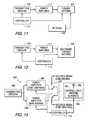
- an RF (radio frequency) probe 400 of FIG. 11senses the radiated power in the near field region of a tunable antenna 404 responsive to the power amplifier 111 .
- An antenna tuning systemsuch as those described herein (including the antenna processor/controller 113 of FIG. 2 ), tunes the antenna resonant frequency to maximize the probe response.
- the tuningmay be in discrete predetermined steps or responsive to maximizing the sensed near field power. Generally, this technique does not compensate for absorption losses in material surrounding the antenna, but corrects for lossless dielectric effects on the antenna resonant frequency.
- Certain communications devices or handsetsare operable according to multiple system protocols (e.g., CDMA, TDMA, EDGE, GSM for a cellular system or Bluetooth or IEEE 802.11x), each protocol assigned to a different frequency band (also referred to as a sub-band).
- system protocolse.g., CDMA, TDMA, EDGE, GSM for a cellular system or Bluetooth or IEEE 802.11x
- each protocol assigned to a different frequency bandalso referred to as a sub-band
- a handsetincludes multiple antennas, with each antenna designated for operation in one of the frequency bands or an antenna capable of multiple resonance behavior.
- the use of multiple antennasobviously increases handset size and a single antenna with multiple resonance behavior is not optimized for any specific frequency, especially if the sub-bands are spaced apart, thereby degrading performance.
- the present inventiontunes a single antenna responsive to the operating sub-band (by activation of the appropriate switch element to change the antenna resonant frequency) when it is desired to operate the handset in a different frequency band, e.g., in response to a different cellular protocol.
- a handset controllerautomatically controls the antenna resonant frequency by selecting the appropriate DC voltage for the varactor diode 350 (or another device that presents a controllable capacitance) such that the antenna resonant frequency is within the selected operating band.
- Such a multiband antenna according to the present inventionis depicted by a multiband tunable antenna 450 of FIG. 12 .
- Operational parameters the multiband antenna 450are controlled in response to a signal, supplied from the controller 110 , indicating a current operating sub-band of the communications device.
- the impedance presented by the antenna 450changes and may not be an optimal impedance for the PA 111 , i.e., provide a load impedance that permits the PA to operate at a desired PAE.
- An optimal impedanceis less likely if the multiple bands are significantly spaced apart in frequency.
- Such a scenariomay arise in a handset where there is a marked decrease in power amplifier PAE when switching from operation on the GSM band (880-960 MHz) to operation on the CDMA band (82-894MHz).
- the VSWRcan increase and the PAE can decline when operation switches to the second frequency band.
- both the resonant frequency and the antenna impedancecan be controlled to improve operation of the communications device, including the PAE of the PA.
- the communications deviceincluding the PAE of the PA.
- the antennaResponsive to a control signal indicating a current operating band or sub-band the antenna is tuned to a different resonant frequency and/or the antenna impedance is modified to present a PA load impedance that raises the PA PAE.
- the frequency tuning and/or impedance adjustmentcan be accomplished by a stub tuner or combinations of lumped and distributed elements, modifying the antenna impedance to improve the PA PAE for a requested PA output power level or retuning the antenna back to its desired resonant frequency.
- the antenna resonant frequency and/or impedancecan be changed by modifying one or more of the antenna's effective electrical length, inductance or capacitance, including modification of these features by using one or more lumped capacitance or inductance elements, or using the various techniques described herein.
- antenna band tuning as implemented by the elements of FIG. 12increased the PA PAE by about 9%; PAE increases up to about 20% have also been observed.
- antenna frequency tuning capabilitypermits reduction of the antenna volumetric size (the reduction estimated to be about 1 ⁇ 2) due to the reduced bandwidth requirement, as the antenna is required to resonate in only one band or sub-band at any time. Simulations indicate that in certain applications antenna resonant frequency tuning alone may produce the desired PAE gain, without the need to control the antenna impedance, i.e., the PA load impedance, while maintaining sufficient bandwidth to cover each band or sub-band, thereby taking advantage of the potential for reduced antenna volume.
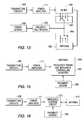
- FIG. 13illustrates another embodiment of the present invention wherein an impedance of one or both of a filter 460 and an antenna 465 are controllable to improve the PAE of the power amplifier 111 as the power amplifier output power changes as described above.
- a switch assembly 462selects elements of the alter 460 to effect a filter input impedance change.
- a switch assembly 464selects elements of the antenna 465 to effect an antenna impedance change.
- the filteris controlled in accordance with its filtering functions, e.g., filtering out-of-band harmonic frequencies within a frequency band with minimal insertion loss. Controlling the filter also assists in presenting a desired PA load impedance (in conjunction with the antenna impedance) to achieve the desired PA PAE.
- any of several different signals produced by the communications devicecan be used to control the switch assemblies 462 and 464 .
- a control signal derived from a power sensor 468is supplied to an encoder/multiplexer 470 for producing a control signal for each switch assembly 462 and 464 .
- the switches 462 and 464(illustrated as mechanical switches but implantable as electronic, mechanical or electromechanical switches) are configured to present the desired impedance for their respective controlled devices.
- Techniques and components for controlling the antenna impedance as described elsewhere hereincan be applied to the FIG. 13 embodiment to control the filter input and/or output impedances and the antenna impedance.
- FIG. 14illustrates certain elements of a dual-band communications device 480 capable of operating in both the GSM band of 850/960 MHz and in the GSM band of 1800/1900 MHz.
- the signal to be transmittedis supplied to an antenna 484 though a power amplifier 486 and a properly configured transmit/receive control switch 487 .
- the signal to be transmittedis supplied to the antenna 484 through a power amplifier 488 and a different configuration of the transmit/receive control switch 487 .
- the antenna 484comprises a radiating structure 490 and controllable antenna elements 491 that permit adjustment of the antenna's resonant frequency and/or its impedance.
- a control signal supplied by the controller 110controls the power amplifiers 486 / 488 and the controllable antenna elements 485 responsive to the desired operating band or sub-band and the PA output power.
- the control signalcontrols the elements 485 to present an antenna impedance that provides a desired PAE for the PA's 486 / 488 .
- the control signalcontrols the elements 491 to present an antenna resonant frequency within the operating frequency band or sub-band.
- the teachings of the present invention as described in conjunction with the communications device 480also applicable to other signal transmission protocols, i.e., EGSM, CDMA, DCS, PCS, EDGE etc. and other non-cellular communications systems and protocols.
- Providing the capability to tune the antenna in a communications devicealso permits use of smaller antenna structures while the antenna structures (and their associated components, such as the PA) operate at a higher PAE than prior art antennas.
- a smaller antennaexhibits a narrower bandwidth, but if the antenna resonant frequency is controllable to a current operating band of the communications device, then a wide band antenna capable of acceptable operation in all frequency bands in which the communications device operates is not required.
- a smaller (and therefore likely more efficient) antennacan be employed in the communications device if the antenna's operating band or sub-band is selectable responsive to the operating band or sub-band.
- a position of the transmit/receive control switchcommands the antenna to change its resonant frequency to the operative sub-band depending on whether the wireless device is in the transmit or receive state.
- This techniqueallows most antennas to be reduced in volume by about a factor of 1 ⁇ 2 and commensurately increases the antenna's PAE.
- a communications device processorselects either the receive or the transmit portion of the band (sub-band) depending on the handset operational mode and supplies a control signal to the antenna to alter one or more antenna parameters, by techniques described herein, to modify the antenna resonant frequency and/or the antenna impedance. Since the sub-bands have a narrower bandwidth than the full band over which the communications device operates, antenna size can be reduced according to this embodiment.
- the embodiments of the present inventionpermit use of a smaller antenna within the communications device, while improving antenna performance (e.g., PAE) over the operating bandwidth.
- antenna performancee.g., PAE
- the ability to alter or select antenna performance parameters (e.g., resonant frequency) in response to an operating frequency of the communications deviceobviates the requirement for an antenna that is capable of operating in all possible bands, and further permits use of a smaller adaptive antenna without sacrificing antenna performance.
- antenna performancemay be improved.
- constructing a smaller antenna and using the teachings of the present invention to improve its performanceovercomes the known performance limitations of the smaller antenna.
- the processorcan improve the feed point, ground point, impedance, antenna configuration or antenna effective length for a given operating condition (e.g., signal polarization or signal protocol) or operating frequency.
- Advantages obtained according to the present inventionare: 1) smaller antenna size; and 2) improved antenna PAE over the operating bandwidth due to adaptive control of the antenna configuration based on the current operating bandwidth.
- Antenna tuningcan also overcome the detuning due to hand or other proximity effects. It is well known that antenna frequency can shift when the user brings body parts or other objects in proximity to the handset or wireless communications device. Two physical phenomena occur in that case, both resulting in poorer handset signal reception and transmission. The first effect is detuning of the antenna resonance caused by proximal capacitive loading of the antenna. The second is absorption of signals caused by resistive loss mechanisms (including complex-valued dielectric constants) associated with dielectric properties of the proximate biological or other substances (wood, paper, water, etc.).
- the present inventionactively tunes the antenna, but may not correct for the aforementioned loss due to absorption of the radiated field components. Nevertheless, this approach improves the handset receive or transmit performance by several decibels.
- Current reduction of radiated signal performance due to hand/head loadingis typically from ⁇ 3 dBi to over ⁇ 10 dBi. Estimates are that 4 dB or more added gain may result from the near field controlled tuning technique of the present invention.
- This embodimentcan be implemented by altering the inductive or capacitive tuning elements in the antenna, such as by controlling frequency tuning and impedance controlling elements 502 of an antenna 504 responsive to a proximity sensor 506 , as illustrated in FIG. 15 .
- the embodimentcan also be implemented by changing the effective electrical length of the antenna as described above.
- the proximity sensor 506supplies a control signal to an antenna impedance control circuit 512 (see FIG. 16 ) for controlling the impedance seen by the power amplifier 111 into an antenna 514 or for controlling the resonant frequency of the antenna 514 .
- the proximity sensor 506comprises a sensor that detects the presence of the body or a body part using an optical sensor, a capacitive sensor or another sensing device. In response to that control signal, the antenna is tuned to a predetermined frequency to offset the detuning caused by the proximate object and partially compensating the loss due to the detuning.
- the proximate sensoris replaced with a near-field RF probe for supplying a control signal that tunes the antenna to maximize the near field signal.
- the senor 506comprises a component for detecting a configuration of a handset communications device.
- a slider type handset and a flip type handsetcan be in an open or closed position, influencing operation of the antenna 504 .
- the antennacan be controlled to improve antenna and handset performance.
- the present inventioncomprises an antenna resonant frequency tuning component for use during manufacture of the communications device to reduce resonant frequency variations in the manufacturing processes.
- Such a resonant frequency tuning componentcomprises a plurality of tuning components (a matrix of components, for example) such as the frequency tuning and impedance controlling elements 117 (see FIG. 2 ) or the tunable antenna 404 (see FIG. 11 ) as described above, that are controllable to compensate the expected range of resonant frequency and bandwidth variability resulting from production variations.
- the tuning componentsare configured to set the desired resonant frequencies for optimum performance MAE, VSWR, etc).
- a tuning matrixcomprises a passive assembly with fusible links that are opened (blown) to insert matrix components into the antenna circuit.
- active device switchescontrol field effect transistors, micro-electro-mechanical systems (MEMS) or other switch technologies known in the art) are utilized to insert components into the antenna circuit by closing one or more of the switching devices.
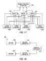
- FIG. 17illustrates a primary radiating structure 550 of an antenna.
- Switches 552e.g., fusible links, transistor switches
- the switchescan be permanently opened or closed after manufacturing and testing the primary radiating structure 550 to overcome the effects of manufacturing variations.
- the switches 552are controlled by a controller associated with a communications apparatus with which the primary radiating structure 550 operates, the controller responsive to operating characteristics of the communications apparatus to control the switches 552 and thereby control operation of the antenna, in particular, the antenna resonant frequency and impedance.
- each of the diverse antennasincludes components to effectuate a change in reactance or a change in effective electrical length to control the antenna resonant frequency.
- a communications device 600includes two antennas 602 and 604 , each responsive to an antenna controller 610 and 612 for controlling the respective antenna resonant frequency and/or impedance according to the various teachings and embodiments of the present invention.
- a diversity controller 618determines which one of the antennas 610 and 612 is operative at any given time (in the receive mode, the signals can be combined to produce a composite received signal).
- a processor executing an appropriate algorithmcontrols the antenna controllers 210 and 212 and the diversity controller 218 to improve a signal quality metric of the communications device.
- FIGS. 19-21illustrate additional configurable or controllable antennas that offer the capability to overcome or at least reduce the effects of undesirable conditions within the antenna's operating environment.
- An antenna 700 in FIG. 19comprises a meanderline structure 702 further comprising a plurality of meanderline segments 702 A, a first terminal end connected to a feed 704 and a second terminal end connected to a radiating structure 706 .
- Exemplary taps 710 connected to one or more of the meanderline segments 702 Aare connected to ground by closing an associated switch 714 under control of an antenna controller 718 . Connecting one or more of the meanderline segments 702 A to ground influences one or more of the antenna resonant frequency, bandwidth and input impedance.
- the meanderline structure 702is a slow wave structure where the physical dimensions of the conductor comprising the meanderline structure 702 are not equal to its effective electrical dimensions.
- a slow-wave conductor or structureis defined as one in which the phase velocity of the traveling wave is less tan the free space velocity of light.
- the frequencyremains unchanged during propagation through the slow wave meanderline structure 702 , if the wave travels slower (i.e., the phase velocity is lower) than the speed of light in a vacuum (c), the wavelength of the wave in the structure is lower than the free space wavelength.
- the slow-wave structurede-couples the conventional relationships among physical length, resonant frequency and wavelength, permitting use of a physically shorter conductor since the wavelength of the wave traveling in the conductor is reduced from its free space wavelength.
- the feed 704is connected to receive and transmit circuits 720 via a 1xX RF switch 722 of the communications device operative with the antenna 700 .
- the receive and transmit circuits 700known in the art, comprise one or more low noise amplifiers and associated receiving, demodulating and decoding components for determining the information signal from a signal received by the antenna 700 , and further comprise one or more power amplifiers, modulating and coding components producing a transmitted signal responsive to an information signal.
- Certain components of the receive and transmit circuits 720are frequency sensitive and thus for optimum performance of the communications device the appropriate frequency sensitive components must be selected responsive to the operating band and mode of the communications device.
- the 1xX switch 722controlled by a control signal provided by the circuits 720 over a control conductor 724 or by a control signal from the antenna controller 718 , provides the capability to connect the antenna 700 to the appropriate frequency-sensitive components of the receive and transmit circuits 700 . Additionally, it is desired to configure the antenna controller 718 to improve performance of the antenna 700 responsive to the operational mode of the communications device. For example, when the communications device is operative in a receive mode in a first frequency band, the 1xX switch 722 is configured to connect receiving components optimized for operation in the first frequency band to the antenna 700 .
- the antenna controller 718is configured to control the switches 714 to improve operation of the antenna 700 for receiving signals in the first frequency band.
- optimization of antenna performancesuggests that the switches 714 are configured to present an antenna impedance that improves PAE of the operative receiving circuits 720 .
- the antenna 700 of FIG. 19is formed on or within a dielectric substrate.
- the permittivity and the permeability of the dielectric material comprising the substrateaffect the properties of the meanderline structure 702 , and thus the properties of the antenna 700 .
- the antenna 700can be formed as a module for simplified insertion and connection to the associated circuits of a communications device, such as the handset or communications device 240 of FIG. 6 .
- Use of the module antennaalso promotes repeatability during the manufacturing process to ensure proper physical placement and connection of the antenna.
- the switches 714are implemented by connecting one or more of the taps 710 to ground trough an inductor (not shown) to establish a DC ground for each tap 710 .
- an antenna 750comprises a configurable signal feed structure comprising the meanderline structure 702 .
- Antenna operating characteristicse.g., antenna impedance, gain, radiation pattern
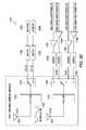
- FIG. 21illustrates an antenna 800 comprising a meanderline structure 802 further comprising a plurality of meanderline segments 802 A and exemplary switches 808 controlled by the antenna controller 718 to provide discrete resonant frequency tuning of the antenna 800 .
- the meanderline structure 802forms a portion of the antenna and therefore influences the antenna parameters, including the resonant frequency
- shorting one or more of the meanderline segments 802 Achanges the resonant length and thus the resonant frequency of the antenna 800 .
- One or more of the switches 808can be closed to tune the antenna 800 to a desired frequency.
- tuning by operation of the switches 808results in discrete, rather than continuous, tuning of the resonant frequency.
- the 1xX switch 722is controlled to connect the appropriate frequency-sensitive components of the receive and transmit circuits 720 to the antenna 800 , responsive to the current operational parameters of the communications device.
- the resonant frequency of the antenna 800is also controlled by configuring the switches 808 , under control of the antenna controller 718 , to establish an antenna resonant frequency that is the same as the operating frequency of the selected frequency-sensitive components.
- the various switching elements identified in FIGS. 19-21can be implemented by discrete switches (e.g., PIN diodes, control field effect transistors, micro-electro-mechanical systems, or other switching technologies known in the art).
- the switching elementscan comprise organic laminate carriers attached to the antenna to form a module comprising the antenna (e.g., the meanderline structures and the radiating structures), the controlling switches and the 1xX switch on a single dielectric substrate.
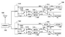
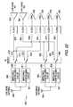
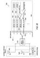
- FIG. 22illustrates a band switched antenna structure 900 comprising respective low band and high band antennas 902 and 904 .
- Impedance controlling circuits 906 and 907connect the low band antenna 902 to a switching terminal 908 of a radio frequency (RF) switch 910 .
- RFradio frequency
- Respective transmit and receive terminals 912 and 914 of the RF switch 910are connected respectively to a serial connection of a low band power amplifier 920 and a filter 922 , and to a serial connection of a first band low noise amplifier (LNA) 928 and a filter 930 .
- LNAfirst band low noise amplifier
- Respective transmit and receive terminals 932 and 934 of the RF switch 910are connected respectively to the serially connected low band power amplifier 920 and filter 922 and to the serially connected second band LNA 938 and filter 940 .
- a switching terminal 941is operable to select either the input terminal 932 or the input terminal 934 .
- the impedance controlling circuits 906 and 907are dissimilar to a present a selectable antenna (load) impedance to the low band power amplifier 920 that improves its operation.
- the power amplifier 920operates in two frequency bands, each presenting a different PA output impedance. It is therefore desired to provide a selectable impedance (the impedance controlling circuits 906 or 907 ).
- the impedance controlling circuit 906comprises a series connection of a first and a second capacitor at a common terminal, with an inductor connected between the common terminal and ground.
- the impedance controlling circuit 907comprises a series connection of a first and a second inductor at a common terminal, with a capacitor connected between the common terminal and ground.
- different impedance controlling circuitscan be used depending on the impedance of the low band antenna 902 and the impedance of the PA 920 .
- the high band antenna 904is connected to a switching terminal 950 through the impedance controlling circuit 906 and to a switching terminal 954 through the impedance controlling circuit 907 .
- Respective transmit and receive terminals 960 and 962 of the RF switch 910are connected respectively to a serially connected high band power amplifier 964 and filter 966 and to a serially connected third band LNA 970 and filter 972 .
- Respective transmit and receive terminals 978 and 980 of the RF switch 910are connected respectively to the serially connected high band power amplifier 964 and filter 966 , and to a serially connected fourth band LNA 984 and filter 986 .
- the filters 930 , 940 , 972 and 986 associated with the LNA'Sfunction in the conventional manner to remove noise and out-of-band frequency components from the received signal, with the pass band of each filter 930 , 940 , 972 and 986 dependent on the operational band of its associated LNA.
- the operational mode of the switched antenna 900is determined by operation of the communications device with which the antenna 900 functions.
- the switching terminal 908When operating in the low band (i.e., low frequency operation) receive mode, either the switching terminal 908 is configured to connect the low band antenna 902 and the impedance controlling circuit 906 to the filter 930 and the first band LNA 928 , or the switching terminal 941 is configured to connect the low band antenna 902 and the impedance controlling circuit 907 to the falter 940 and the second band LNA 938 .
- a configuration of the switching terminals 908 and 941is controlled by an antenna controller (not shown in FIG. 22 ) based on the operating characteristics of the communications device. In particular, if the communications device can operate in two different low band frequencies, one of the switching terminals 908 or 941 is operative to connect the associated LNA 928 or 938 , respectively, to the low band antenna 902 responsive to the operating low-band frequency.
- the PA 920is connected to the low band antenna 902 through one of the impedance controlling circuits 906 and 907 via the selected configuration of the RF switch 910 , that is via either the terminal 912 or the terminal 932 , as determined by one of the impedance controlling circuits 906 or 907 that improves the PAE of the power amplifier 920 .
- the impedance controlling circuits 906 and 907are also controllable to change the impedance seen by the associated power amplifier to improve the PAE of that power amplifier.
- the switching terminals 950 and 954are controlled to connect either the LNA 970 or the LNA 984 to the high band antenna 904 in the receive mode or to connect the high band PA 964 to the high band antenna 904 through one of the impedance controlling circuits 906 and 907 .
- the communications device designerit is usually the intent of the communications device designer to transform the impedances of the components in the transmit and receive signal paths to a nominal 50 ohms to improve device performance. Since these components are typically individually procured and assembled, the presented impedance values may differ substantially from 50 ohms and the transformation to 50 ohms may result in undesired bandwidth limitations as also discussed above.
- the layout of the components and connecting conductors(which may present other than a 50 ohm impedance) tends to cause the impedance to vary from the desired 50 ohms. Since the load is usually a complex impedance, reactive components or transmission line lengths will change the load at the power amplifier depending on the line length, layout, component selection, filter type, etc. Finally the antenna supplier has no control and little influence over design features and components in the transmit and receive signal paths that can substantially influence antenna performance.
- the present inventionteaches a radio frequency module embedding one or more components of toe serial component string including one or more of transmitting and receiving circuits, a low noise amplifier, a power amplifier, filters and connecting elements connecting these components to the antenna.
- the impedance presented by the module componentsis substantially consistent among all the module components (and likely not the conventional 50 ohms) to improve signal receiving and transmission performance, overcoming the effects of impedance variations and mismatches of the prior art.
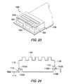
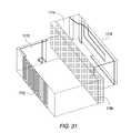
- An exemplary moduleis illustrated in FIG. 23 and described in the accompanying text.
- the modulealso improves power amplifier PAE (resulting in longer talk time between battery charges).
- Use of the modulereduces development time to market and lowers manufacturing and component integration costs since all components are embedded in the module and its fabrication is repeatable.
- a module 1000comprises a front end electronics module 1002 (comprising in one embodiment the impedance controlling circuits 906 and 907 , the RF switch 910 , the filters 922 , 966 , 930 , 940 , 972 and 986 , the power amplifiers 920 and 964 and the low noise amplifiers 928 , 938 , 970 and 984 or any combination of these elements), an organic (or other) laminate material 1004 , the low band and high band antennas 902 and 904 (preferably constructed from an appropriate length of conductive material, including a conductive flex film material and either printed on or subtractively removed from one or more surfaces of the laminate 1004 ) and a carrier 1008 .
- a front end electronics module 1002comprising in one embodiment the impedance controlling circuits 906 and 907 , the RF switch 910 , the filters 922 , 966 , 930 , 940 , 972 and 986 , the power amplifiers 920 and 964 and the low noise amplifiers
- the passive components of the impedance controlling circuits 906 and 907 and the passive components of the filters 922 , 966 , 930 , 940 , 972 and 984are formed as passive elements within the material of the laminate 1004 .
- Candidate laminate materialinclude known PCB compounds and epoxy materials both with and without the fiber glass filler material.
- Printed circuit board material and flex film materialcan be used in lieu of the organic laminate material.
- the modular switched antenna 900(i.e., the laminate material) is about 28 mm long, about 15 mm wide and about 7 mm high, presenting an antenna volume about one-half to one-quarter the volume of prior art multiband antennas.
- Embodying the various antenna control techniques taught herein in modular formprovides more efficient packaging, simpler insertion into a communications device, lower cost, better reliability and better performance.
- the design and layout processes associated with use of the module in the communications deviceare substantially reduced.
- the selectable/controllable/tunable features of the various antenna embodiments described hereinprovide a higher PA PAE over the operating bandwidth than the prior art multiband antennas.
- the transmission line lengths and the impedance presented by the transmission linesare selected to provide the desired impedance transformations between two components connected by the transmission lines.
- active tuning of the antenna as described hereinpresents an impedance to the PA via the duplexer intermediate the antenna and the PA.
- the various schemes according to which the phase, amplitude and/or impedance of the antenna are adjusted to improve the PAEcan take into account the transmission characteristics of the duplexer and associated interconnect transmission lines to the antenna and the PA.
- the frequency-dependent characteristics of the duplexercan therefore be considered when adjusting the antenna impedance.
- frequency variant tuning of the duplexercan be employed, in addition to tuned elements at the antenna.
- power dependent tuning of the duplexer itselfcan be used as well.
- the antennaAs a result it is preferred to include the antenna, phase/amplitude/impedance tuning components, duplexer, and associated control components as part of a module, such as the module 1000 of FIG. 23 .
- the modulefunctions, as described, to present a load to the PA at operating frequencies that optimizes the PA efficiency.
- some degree of mistuningmay be employed to adjust for antenna proximity effects (e.g., proximate relation of the users had and body to the antenna) during operation.
- tuning components at the antennais also an acceptable solution for many problems currently encountered in portable device RF design for CDMA systems.
- the functions described abovesuch as optimizing the PA efficiency for GSM operation, timing to maintain antenna resonance in the presence of proximal dielectrics (human body, tables, etc), band-selectable tuning (no sub bands in CDMA) to allow reduction of the antenna physical volume, and frequency, tuning to present a more constant impedance (better match) versus operating frequency, are all possible byproducts of the inclusion of tuning components.
- antenna spatial diversityis achieved by selectively driving a radiating structure 1100 , see FIG. 24 , from either a terminal end 1104 or a terminal end 1108 .
- a meanderline radiator structureis illustrated as merely an exemplary embodiment.
- a feed 1114is coupled to the terminal end 1104 , resulting in a current minimum at the terminal end 1108 and a current maximum at the terminal end 1104 .
- Reconfiguring the switch 1112 to a configuration 1112 B and configuring the switch 1120 closing the switch 1120shifts the current maximum to the end 1108 and the current minimum to the end 1104 .
- Changing the location of the current maximum and current minimumalters the antenna pattern (phase center) to achieve spatial diversity.
- the switches 1112 and 1120are controlled by control signals generated in other elements of the communications device. For example, if the signal-to-noise ratio of the received signal falls below an identified threshold (or the bit error rate of the received signal exceeds a predetermined threshold) the switch configurations are reversed in an effort to improve performance.
- one embodiment of a conventional communications device operative with a single antennaemploys a serial component string (signal path) comprising the power amplifier (and the low noise amplifier in the receiving mode), a switch plexor (for use with the GSM protocol) or duplexer (for use with the CDMA protocol) the antenna impedance controlling element and the antenna.
- the switch plexor or duplexerswitches into the serial string of the appropriate power amplifier or low noise amplifier responsive to operating conditions.
- an actual nominal antenna impedancecan range between about 20 ohms and several ohms as a function of frequency over its operating bandwidth.
- the output impedance of the power amplifieris typically a few ohms (about 3 to 7 ohms and usually complex) and varies with output power as described above.
- the antenna impedanceis transformed to an impedance that improves the power amplifier PAE.
- the optimum impedanceis selected from a locus of points that are generated as a function of the signal frequency supplied to the antenna and the commanded RF power output from the PA.
- the optimum impedanceis the value that allows the power amplifier to operate at optimum PAE, i.e., producing an output signal that uses the available supply voltage/current without signal clipping or saturation.
- the power amplifier impedanceis transformed to about 50 ohms. It is therefore desired for the antenna to present a 50 ohm impedance (by transforming the antenna radiation resistance, typically about 15 ohms, to 50 ohms) such that when connected by a 50 ohm transmission line to the power amplifier, the antenna provides a satisfactory load for the PA.
- a 50 ohm impedanceby transforming the antenna radiation resistance, typically about 15 ohms, to 50 ohms
- the antennaprovides a satisfactory load for the PA.
- the power amplifier output impedanceis not transformed to 50 ohms, but instead to a value close to the antenna radiation resistance or to an intermediate value between 50 ohms and the PA output impedance.
- the impedances of both the power amplifier and the antennaare transformed to the filter impedance. Transforming to an impedance lower than 50 ohms reduces the concomitant bandwidth reduction as the ratio of the two impedances is lower.
- FIG. 25illustrates this aspect of the invention in which a alter and/or switch plexer 1150 is interposed between a power amplifier 1152 and an antenna 1154 .
- Preferably all of the series equivalent characteristic impedance values, no m, p and qare less than 50 ohms.
- the bandwidth reduction associated with these impedance transformationsis less than the prior art systems where all the impedances are transformed to 50 ohms. It is also possible to design an antenna to provide a closer impedance match to the output impedance of the PA, thereby eliminating the need impedance transform to an artificially specified value, thereby optimizing the performance of the PA, filter, switchplexer (or diplexer) and elements in the antenna chain. The benefit of this approach is lower loss in the transmission and receiving paths and greater bandwidth.
- the various elements illustrated in FIG. 25are formed as a radio frequency antenna/power amplifier module, comprising a dielectric material surrounding an integrated circuit, wherein the electronic components of the elements 1150 , 1160 and 1164 are formed within the integrated circuit.
- a fixed pre-positioning of the PA 1152 relative to the other components included within the moduleprovides the best performance for the modularized elements.
- the filter components of the element 1150may be implemented as passive components within the module, and therefore are not necessarily formed in the integrated circuit.
- a PA load impedance that improves the PAE over an appropriate bandwidthis determined.
- the impedance of one or more of the module elementsis transformed to present that load impedance to the PA and the impedance transformation components 1160 and 1164 are controlled to match impedances between elements (except the PA 1152 ).
- FIG. 26Another embodiment of the present invention teaches modularization of a front end module (FEM) 1200 illustrated in block diagram form in FIG. 26 .
- the FEM 1200comprises an antenna 1204 and routing switches 1206 .
- a receive pathcomprises a receive filter 1208 and a low nose amplifier 1210 .
- a transmit pathcomprises a transmit filter 1214 and a power amplifier 1218 .
- the FEM 1200further comprises the impedance transformation components illustrated in FIG. 24 for improving the bandwidth response of the FEM 1200 .
- the LNA 1210 and the PA 1218are firer connected to an RF integrated circuit (RFIC) 1230 comprising conventional components associated with processing the outgoing signal in the transmit mode and the incoming signal in the receive mode, e.g., up and down frequency conversion, modulation and demodulation and signal frequency synthesis.
- RFICRF integrated circuit
- a baseband processor 1240decodes the baseband signal provided by the RFIC 1230 in the receive mode co produce the information signal.
- the baseband processor 1240encodes the information signal and supplies the encoded signal to the RFIC 1230 .
- the baseband processor 1240receives the baseband signal from the RFIC 1230 , decoding same to produce the information signal.
- FEM 1200Use of the FEM 1200 reduces time-to-market for the manufacturer of the communications device since the components and functionality are conveniently supplied in modular form. Reduced manufacturing costs (fewer components to inventory and track, simpler designs required) and manufacturing repeatability are also realized by use of the FEM 1200 .
- the FEM 1200incorporates the beneficial dynamically selected antenna impedance values for loading the PA at different power levels, thus improving PA operating PAE, as described above.
- PAE improvementswhich have been shown by the inventors to be 10% to 20%, lengthen the handset “talk” time as battery life is extended.
- the teachings of the present invention related to antenna impedance controlcan also be applied to control the VSWR of the signal provided by the PA to the antenna for transmission.
- An actual VSWRcan be measured by known techniques and compared to a desired VSWR.
- the antenna impedanceis controllable responsive to the actual VSWR to achieve the desired VSWR.
- FIGS. 27-29illustrate various antenna and related components suitable for use with a CDMA communications protocol
- FIG. 30illustrates an antenna isolation technique suitable for use with certain embodiments of the present invention
- FIGS. 31 and 32illustrate antennas and related components suitable for use with a GSM communications protocol.
- FIG. 27illustrates a transmitting and receiving system 1500 suitable for use with the CDMA air interface.
- the system 1500comprises a high band antenna 1502 operative generally in the frequency bands of about 1850-1910 MHz (uplink) and 1930-1990 MHz (downlink) and a low band antenna 1506 operative generally in the frequency band of about 824-849 MHz (uplink) and 869-894 (downlink).
- a CDMA uplink signalis transmitted (for example from a handset to a base station) on one of the uplink frequencies and the downlink signal (for example from the base station to the handset) is transmitted on one of the downlink frequencies.
- the system 1500 of FIG. 27is capable of sending and receiving signals in either of the high or low frequency bands. But since the transmit and receive functions use the same antenna an isolating device (a duplexer for example) is required to isolate the transmit and receive paths.
- a high band receiver 1510is connected to the high band antenna 1502 via a serial connection of an impedance matching network 1514 and a duplexer 1518 .
- the matching network 1514matches the high band antenna impedance (as transformed through the duplexer 1518 ) to 50 ohms, since the high band receiver typically operates from a 50 ohm input.
- the matching network 1514matches a 20 ohm antenna impedance to 50 ohms.
- impedance matching network 1514can be designed to accommodate matching of various impedance values, it is known that impedance matching tends to reduce the signal bandwidth in direct proportion to the difference between the two impedance values that are matched, unless complex multistage matching elements are employed.
- the system 1500further comprises a high-power amplifier 1530 (providing an output power P 1 ) connected to the high band antenna 1502 via a serial string of a matching network 1534 , a switch 1538 and the duplexer 1518 .
- a low-power amplifier 1540 providing an output power P 2 )is also connected to the high band antenna 1502 via a serial string of a matching network 1544 , the switch 1538 and the duplexer 1518 .
- the PA output impedancecan range from about 3 ohms to about 2000 ohms.
- the load impedance seen by the power amplifieraffects the power amplifier efficiency.
- the impedance of an antenna connected to the PAis controlled to present an impedance that maximizes the PAE.
- the power amplifier 1530is selected as the operative power amplifier (responsive to a control signal not illustrated and configuration of the switch 1538 to a state 1538 A) when a relatively high-power output signal is required for the effective communications in the high frequency band.
- the PA 1530thus supplies a relatively high-power output signal P 1 .
- an exemplary load impedance of about 3 ohmsmaximizes the PAE of the power amplifier 1530 .
- the matching network 1534it is desired for the matching network 1534 to transform the impedance seen looking into the switch 1538 (for example about 20 ohms as indicated in FIG. 27 ) to about 3 ohms to maximize the PAE of PA 1530 .
- the PA 1540is operative, as controlled by a control signal not illustrated in FIG. 27 and configuration of the switch 1538 to a state 1538 B, to deliver a low-power output signal P 2 . Due to the difference in the power of the signals P 1 and P 2 , the optimum load impedance for maximizing the PAE of the PA 1540 is different than the optimum impedance for maximizing the PAE of the PA 1530 .
- the impedanceis indicated to be greater than about 3 ohms and can range to about 2000 ohms dependent on the power in the output signal P 2 .
- the matching network 1544transforms the exemplary switch/antenna impedance of about 20 ohms to the PA 1540 output impedance to maximize its PAE.
- the power amplifiers 1530 and 1540are described as supplying a discrete output power level P 1 or P 2 that determines the load impedance for maximum PAE, it is known by those skilled in the art that the teachings of the invention apply to other output power levels and output impedance values.
- the power amplifiersoperate to supply output signals having a power level different than the exemplary P 1 and P 2 power levels, and thus different load impedance values are required to optimize the PAE of the power amplifiers.
- the duplexer 1518must provide sufficient isolation between the signals present at its two input ports 1518 A and 1518 B, since according to the CDMA protocol the transmitting and receiving components may be simultaneously active. Thus duplexer isolation prevents the transmitted signal from bleeding into the receive components and the received signal from bleeding into the transmit components.
- the duplexer 1518When the system 1500 is operating in a receive mode, the duplexer 1518 must present a relatively high impedance at the terminal 1518 A. Similarly, when the system 1500 is transmitting through the high band antenna 1502 a relatively high impedance is seen at the terminal 1518 B.
- the low-band antenna 1506is similarly connected to a duplexer 1560 having a port 1560 A connected to a serial sting of a matching network 1564 and a low-band receiver 1568 .
- a port 1560 B of the duplexer 1560is connected to a common terminal 1572 A of a switch 1572 .
- a terminal 1572 B of the switch 1572is farther switchably connected to a serial string comprising a matching network 1576 and a high-power amplifier 1580 (supplying a relatively high-power output signal P 3 );
- a terminal 1572 Cis switchably connected to a serial string comprising a matching network 1584 and a low-power amplifier 1588 (supplying a relatively low-power output signal P 4 ).
- the matching networks 1576 and 1584see the impedance of the low-band antenna as transformed through the duplexer 1560 and the switch 1572 , and transform this impedance to increase the PAE of the operative high-power amplifier 1580 or the low-power amplifier 1588 .
- a load impedance of about 3 ohmsmaximizes the PAE of the PA 1580 at the power level of the signal P 3 and a load impedance of greater than about 3 ohms maximizes the PAE of the PA 1588 .
- the impedance values set forth in FIG. 27are merely exemplary, although it is expected that the output impedance of a low power amplifier ( 1540 and 1588 ) would be greater than the output impedance of a high power amplifier ( 1530 and 1580 ).
- the design of the high-band and low-band antennas, the duplexers, the receivers, the power amplifiers, and the switchesall impact the impedances seen at the matching network terminals. Further, the power level of the power amplifier output signals determine the load impedance that maximizes the PA PAE. It is generally known, however, that duplexer size increases when designed to operate into a lower impedance load or source impedances. It is therefore preferable to use relatively large impedances in conjunction with the duplexers of FIG. 27 to maintain a reasonable duplexer size for use in a communications device, especially for use in hand held communications devices.
- the matching networks 1514 and 1564are both indicated as matching to a presented 20 ohm source impedance. But in another embodiment the high and low band antennas 1502 and 1506 may present different impedances at resonance and thus the matching networks 1514 and 1564 may see different source impedances for transformation to a suitable impedance for their respective receiver 1510 and 1568 .
- each of the antennas 1502 and 1506comprises an antenna presenting a relatively low impedance.
- signal bandwidth lossis reduced compared with an embodiment employing antennas that present a 50 ohm impedance at resonance. Since the impedance seen from the input terminal of each of the matching networks 1534 , 1544 , 1576 and 1584 is lower when low impedance antennas are used, the difference between the input and output impedances is reduced and the bandwidth of the impedance transformation is therefore increased.
- the antenna impedanceis switched between receive and transmit functions to reduce the impedance transformation ratio required between the antenna and the receiver.
- the switches 1538 and 1572present a sufficiently low resistance to limit the power losses they introduce into the signal path.
- the matching networks 1514 , 1534 , 1544 , 1576 and 1584may comprise both impedance transformation components and signal filter components. Further, the receivers 1510 and 1568 (and the other receivers illustrated in the various Figures) may comprise both receiver and filter functionalities.
- the components illustrated in FIG. 27are fabricated in a modular form, with the electronics components disposed within a dielectric substrate and the antenna components disposed on outer surfaces of the substrate.
- FIG. 28illustrates a system 1598 sharing certain common elements with the system 1500 of FIG. 27 and suitable for CDMA operation.
- the system 1598comprises a single antenna 1600 connected to the duplexers 1518 and 1560 through a combiner 1602 , which in one embodiment is an element of the antenna structure. Operation of the combiner 1602 is frequency dependent such that high band received signals are supplied from the antenna 1600 to the duplexer 1518 and low band received signals are supplied from the antenna to the duplexer 1560 .
- one of the high-power amplifiers 1530 and 1580(preferably optimized for supplying a signal in the high-band spectrum) or the low-power amplifiers 1540 and 1588 preferably optimized for supplying a signal in the low-band spectrum) can supply a signal to the combiner (through their respective duplexers 1518 and 1560 ) for transmission by the antenna 1600 .
- FIG. 29illustrates a system 1720 including a receive antenna 1721 and a transmit antenna 1722 appropriately isolated by an isolation structure 1723 as farther described below.
- Either the high-band receiver 1510 or the low-band receiver 1568is connected to the receiving antenna 1721 via a filter 1724 , a switch 1725 and respective matching networks 1726 and 1728 .
- the matching networksmay be required to match an impedance of the receivers 1510 and 1568 (which may not be identical) to a source impedance seen looking into the switch 1725 .
- the matching networks 1726 and 1728typically match to different impedance values Z10 and Z11 ohms as indicated.
- the system 1720is applicable to CDMA systems where the switch 1725 is controlled to a state to receive signals depending upon whether the signal is in the CDMA high band (1930-1990 MHz) or the CDMA low band (869-894 MHz).
- a filter 1740 , a switch 1744 and respective matching networks 1748 and 1752are responsive to a signal supplied by a high-band power amplifier 1754 and by a low-band power amplifier 1756 :
- the frequency-dependent filters 1724 and 1740can provide additional isolation between the receive and transmit operating frequencies, i.e., in addition to the isolation provided by the isolation structure 1723 .
- the power amplifiers 1754 and 1756may operate at different output power levels and therefore to maximize the PAE they may be operated at different load impedances, Z12 and Z13 ohms as indicated in FIG. 29 .
- the matching network 1748transforms an impedance of Z14 ohms to Z12 ohms for the high band-power amplifier 1754 and the matching network 1752 transforms an impedance of Z15 ohms to Z13 ohms for the low-band power amplifier 1756 .
- the transmit antenna 1722presents a high-band impedance when operating at a high-band frequency and a different low-band impedance when operating at a low-band frequency.
- the impedances Z 14 and Z 15may not be equal.
- the matching networks 1748 and 1752are controllable to present different load impedances to the power amplifiers 1754 and 1756 to optimize or at least improve the PAS of each power amplifier 1754 and 1756 (i.e., improve the PAE or efficiency over the efficiency absent use of the controllable matching networks 1748 and 1752 .)
- the transmit and receive antennas 1721 and 1722 , the filters 1723 and 1740 , and the switches 1724 and 1744can be incorporated into a single antenna module. In another embodiment, only the receive and transmit antennas 1721 and 1722 are incorporated into the module.
- FIG. 30illustrates a system 1757 derived from the system 1720 of FIG. 29 and further comprising a high-band high-power PA 1760 , a high-band low-power PA 1761 , a low-band high-power PA 1762 and a low-band low-power PA 1763 and their respective matching networks 1764 , 1765 , 1766 and 1767 .
- a switch 1768selectably connects one of the PA's 1760 , 1761 , 1762 and 1763 to the transmit antenna 1722 via the filter 1740 .
- the matching networks 1764 , 1765 , 1766 and 1767are configured (either a fixed or a controllable configuration) to provide a load impedance to the PA's 1760 , 1761 , 1762 and 1763 to maximize the PAE of each PA according to the operating power level (or another power-related parameter, for example, a power amplifier output power, an operating frequency of a communications device operative with the system 1757 wherein operation of the power amplifiers is responsive to the operating frequency of the communications device or a voltage standing wave ratio on a conductive path between the power amplifier and the transmitting antenna) of the PA.
- the operating power levelor another power-related parameter, for example, a power amplifier output power, an operating frequency of a communications device operative with the system 1757 wherein operation of the power amplifiers is responsive to the operating frequency of the communications device or a voltage standing wave ratio on a conductive path between the power amplifier and the transmitting antenna
- FIG. 31illustrates an example of the isolation structure 1723 of FIGS. 29 and 30 .
- a dielectric substrate 1770supports an antenna 1772 (in this exemplary embodiment the antenna 1772 comprises a meanderline antenna) and a dielectric substrate 1776 supports an antenna 1778 (in this exemplary embodiment the antenna 1778 comprises a PIFA antenna).
- An isolation structurecomprises a conductive structure 1880 disposed between the substrates 1770 and 1776 .
- the conductive structurecomprises a generally U-shaped conductive structure.
- the conductive structurecomprises a sheet disposed between the substrates 1770 and 1776 .
- the substrates 1770 and 1776are replaced by a dielectric sheet (a flex film dielectric sheet, for example) with a conductive surface sandwiched between the dielectric sheets.
- the antennas 1772 and 1778are disposed on outside surfaces of the dielectric sheets.
- isolation between the receive and transmit antennas 1721 and 1722is provided by signal polarization diversity, i.e. the two antennas 1721 and 1722 propagate signals with different signal polarizations to achieve the desired isolation.
- signal polarization diversityi.e. the two antennas 1721 and 1722 propagate signals with different signal polarizations to achieve the desired isolation.
- a first antenna propagating a horizontally polarized signal and a second antenna propagating a vertically polarized signalmay provide the desired signal isolation in lieu of the isolation structure 1723 in FIGS. 29 and 30 .
- a system 1850 of FIG. 32is suitable for use with any protocol employing a time division multiple access scheme, such as the GSM protocol, to separate transmit and receive operations.
- a switchplexer 1851comprises a plurality of selectable terminals each responsive to a matching network/filter 1852 , 1854 , 1856 and 1858 .
- the matching network/filter 1852 and 1854are responsive respectively to a high-band receiver 1860 and a low-band receiver 1868 .
- the system 1850further comprises a GPS receiver.
- the matching network/filters 1856 and 1858are responsive respectively to a high-power amplifier 1870 and a low-power amplifier 1872 .
- the PA's 1870 and 1872are combined (e.g., using CMOS (complimentary metal oxide semiconductor field effect transistors) technologies) with a corresponding single matching network/filter configuration.
- CMOScomplementary metal oxide semiconductor field effect transistors
- a configuration of a switch common terminal 1851 Ais controlled according to the operational mode (receive or transmit) and the operating frequency (high band or low band) of the communications device.
- the common terminal 1851 Ais connected to a matching network/combiner 1875 to supply the selected signal to antennas 1880 / 1884 in the transmit mode or to receive signals from the antennas 1880 / 1884 in the receive mode.
- the matching network/combiner 1875may comprise a high and low pass filter to direct the high and low band frequency signals as desired.
- the functionality of the matching network/combiner 1875can be integrated with the antennas 1880 and 1884 using parasitic coupling or direct coupling of different resonant antenna elements.
- the matching network/combiner 1875supplies the received signal to the common terminal 1851 A of the switchplexer 1851 for feeding to either the high-band receiver 1860 via the matching network/filter 1852 or to the low-band receiver 1868 via the matching network/filter 1854 , as determined by the state of the switchplexer 1851 .
- the matching networks/filters 1852 and 1854transform the source impedance they see to the input impedance of the respective receivers 1860 and 1868 .
- the signal to be transmittedis supplied from either the high-power PA 1870 or the low power PA 1872 .
- the maximum PAE of the power amplifiers 1870 and 1872is achieved when the load impedance is Z20 and Z21 ohms, as indicated, respectively.
- the matching network/filter 1856provides the load impedance of Z20 ohms to the PA 1870 by transforming its source impedance (as seen looking into the switchplexer 1851 from the matching network/filter 1856 ) to Z20 ohms.
- the matching element/filter 1858presents a load impedance of Z21 ohms by transforming its source impedance (as seen looking into the switchplexer 1851 from the matching network/filter 1858 ) to Z21 ohms.
- an impedance of each antenna 1880 and 1884is controllable responsive to an antenna impedance controller 1888 further responsive to a control signal.
- controlling the antenna impedance to provide an optimal load impedance for the power amplifiers 1870 and 1872improves the power amplifier efficiency and hence extends battery life of the communications device in which the system 1850 is embedded.
- the control signalcan be derived from a baseband controller representative of the PA output power or by a band select signal that identifies the currently operative band for the communications device.
- the antennas 1880 and 1884are formed on a common substrate or formed on separate substrates and bonded together, forming an antenna module.
- the antenna modulemay be referred to as a viable impedance antenna module since the impedance controller 1888 controls the impedance presented by the antennas 1880 and 1884 .
- Each of the matching networks/filters 1856 and 1858can be controlled in real time responsive to the output power of the respective PA to achieve a desired or maximum PAE.
- each of the matching networks/filters 1856 and 1858can provide a fixed load impedance for the respective PA that will maximize the PAE based on an average or expected value of the output power.
- the matching networks/filters 1856 and 1858operate as band pass filters and provide a fixed impedance suitable for the switchplexer 1851 , while the antenna controller 1888 presents an impedance to maximize the PAE.
- the load impedance of eachcan be controlled by operation of the respective matching network/filter 1856 and 1858 .
- the antenna impedancecan be controlled by the impedance controller 1888 to present a different source impedance to the matching networks/filters 1856 and 1858 , which in turn transform the source impedance to a PA load impedance to maximizes the PAE for each PA 1870 and 1872 .
- the number of receiving and transmitting elements in the system 1850can be easily extended as indicated.
- the receivers, power amplifiers and matching networks/filterscan be manufactured in the form of a module.
- FIG. 33illustrates a system 1900 sharing common elements with the system 1850 of FIG. 32 .
- the system 1900employs a non-50 ohm signal transmission chain as indicated by the exemplary “ ⁇ 20 ⁇ ” designation between the switchplexer common teal 1851 A and a combiner 1904 .
- Antennas presenting such a “low” impedanceare referred to as low impedance antennas and are capable of providing a low impedance over their operating bandwidth.
- the antennas 1880 and 1884are formed on a common substrate or formed on separate substrates and bonded together, forming an antenna module.
- the antenna modulemay be referred to as a low impedance antenna module.
- the matching networks/filters 1852 and 1854transform their source impedance to the load impedance for the high-band and low-band receivers 1860 and 1868 .
- the matching networks 1856 and 1858can transform their source impedance to a load impedance that controls or maximizes the PAE (or efficiency) for the respective power amplifier 1870 and 1872 .
- the matching networks/filters 1856 and 1858provide a controllable range of impedance transformations to provide a range of load impedances for the power amplifiers 1870 and 1872 .
- Certain elements within the various embodiments presented in FIGS. 27-33can be formed or implemented in a module by forming or mounting multiple components on a common substrate.
- the high and low band antennas 1880 and 1884 , the combiner 1875 and the impedance controller 1888 of FIG. 32can be physically combined Into a modular element.
- the high band antenna 1880 , the low band antenna 1884 and the combiner 1904can be combined to form a module in the embodiment of FIG. 33 .
- the switchplexer 1851can also be included within the module.
- other elementsswitching and filters, for example
- the modular implementationprovides fixed interconnections and parts placement that avoids performance degradation from transmission line (conductor) lengths variations, alter characteristic variations and parasitic effects due to coupling between components. Component characteristics are matched at the time of module design, thereby limiting mismatch losses.
- the fixed phase shift through the radio frequency component chain at each operating frequencyis known and can be compensated as required.
- the fixed phase shiftis also beneficial for PA stability over presented mismatches due to environmental effects and changes (e.g., the proximity effect).
- the module's radio frequency portion(i.e., the front end where many of the physical layout-induced performance variations arise) offers known performance characteristics, reducing design time of the communications device and therefore time to market.
- the modular approachcan reduce transmission line length, and thus losses in the transmission lines, as the antenna(s) and power amplifier(s) are located in proximate relationship.
- a high-speed bus(such as an optical fiber) can be used to supply the signal to be transmitted from the baseband/modulating components to the power amplifiers.
- the modularized systemoffers the communications device designer a physically stable and operationally predictable component for insertion into a communications device.
- the power amplifiers of the various presented embodimentshave been described as supplying a signal having a discrete output power level (e.g., signals P 1 and P 2 ) that determines the load impedance for maximum PAE, the teachings of the invention are not so limited and can be applied to other output power levels and to power amplifiers capable of supplying a signal having a power within a range of power levels.
- the load impedance that maximizes the PAEis different dependent on the PA output power of the power amplifier. Therefore, the various presented matching networks, if capable of transforming only a single source impedance to an output impedance may not assure a maximum PAE at all output power levels.
- a matching network that can transform the source impedance to a selectable output impedancemay be preferred to maximize the PAE at all possible PA output power levels.
- FIG. 34illustrates a dual band communications apparatus 2000 comprising the high band receiver 1860 and a high band power amplifier 2006 selectably connected to a high pass filter 2008 via a transmit/receive switching element 2012 .
- the antenna 1880Responsive to a condition of the switching element 2012 , the antenna 1880 , connected to the filter 2008 , supplies a received signal to the high band receiver 1860 or transmits a signal supplied by the power amplifier 2006 .
- the operating mode of the communications apparatus 2000(and the condition of the switching element 2012 ) is controlled by a signal representing the operating mode (receiving or transmitting) of the communications device.
- the communications apparatus 2000 hurtercomprises the low band receiver 1868 , a low band power amplifier 2020 , a switching element 2022 , a low pass filter 2026 and the low band antenna 1884 .
- the components associated with low band operationoperate similarly to those associated with high band operation as described above.
- Use of the filters 2008 and 2026 and the dedicated high band and low band antennas 1880 and 1884 in the communications apparatus 2000avoids the need for a switchplexer, such as the switchplexer 1851 illustrated in FIG. 32 .
- the switchplexeris a relatively expensive element and therefore its elimination is a cost reduction (and space reduction) advantage, especially for low-cost communications apparatuses.
- use of the high band and the low band antennas 1880 and 1884 , respectively,allows each to be designed for optimum performance in its operating band.
- each antenna 1880 and 1884is designed for a 50 ohm match within its operating band.
- the power amplifiers 2006 and 2020prefer a low load impedance and the receivers 1860 and 1868 prefer a higher (source) impedance.
- the high band receiver 1860 and the high band power amplifier 2006are matched to a fixed impedance of 50 ohmns of the antenna 1880 and any intervening components, such as the filter 2008 and the switching element 2012 .
- the low band receiver 1868 and the low band power amplifier 2020are matched to a fixed impedance of 50 ohms of the antenna 1884 and any intervening components, such as the filter 2026 and the switching element 2008 .
- the impedance presented by the antennas 1880 and 1884are controllable, for example by use of the impedance controller 1888 of FIG. 32 , to control the load impedance presented to the respective power amplifier 2006 and 2020 to control the efficiency of the power amplifiers 2006 and 2020 .
- FIG. 35illustrates a communications apparatus 2040 comprising two high band antennas 2008 (one for transmitting and one for receiving), two low band antennas 1884 (one for transmitting and one for receiving), the high pass filter 2008 and the low pass filter 2026 .
- the four antennas and respective filtersprovide an equivalent functionality to the diplexer/switchplexer and the switches of the embodiments described above and can be optimized for performance with the associated power amplifier or receiver.
- Another embodimentincludes the impedance controller 1888 , to control the impedance of the antennas 1880 and 1884 as presented to the respective power amplifier 2006 and 2020 to control the efficiency of the power amplifiers 2006 and 2020 .
Landscapes
- Engineering & Computer Science (AREA)
- Computer Networks & Wireless Communication (AREA)
- Support Of Aerials (AREA)
- Transceivers (AREA)
- Transmitters (AREA)
Abstract
Description
- A. Poor power amplifier CA) efficiency due to sub-optimal PA load impedance (where the antenna impedance is the PA load impedance) as the PA's output power changes during operation of the communications device and as the antenna impedance change as the signal frequency changes.
- B. Poor PA efficiency as set forth in A. above as further affected by the antenna's relatively narrow bandwidth due its relatively small size to fit within the available space envelope of the communications device (i.e., the Chu-Harrington limitation).
- C. Poor PA efficiency due to a sub-optimal PA load impedance as the hand-effect or proximity effect detunes the antenna resonant frequency and/or modifies the antenna impedance.
- D. Loss of radiative energy transfer (coupling efficiency) due to a sub-optimal PA output impedance (i.e., a sub-optimal antenna impedance) due to the use of a relatively small antenna and it corresponding relatively narrow bandwidth.
- E. Loss of radiative energy transfer (coupling efficiency) due to detuning of the antenna resonant frequency caused by the hand-effect or proximity effect.
- F. Poor PA efficiency due to impedance transformation to a higher value (i.e., 50 ohms) versus a lower value closer to the natural radiation resistance of the antenna.
Claims (3)
Priority Applications (3)
| Application Number | Priority Date | Filing Date | Title |
|---|---|---|---|
| US11/623,307US8000737B2 (en) | 2004-10-15 | 2007-01-15 | Methods and apparatuses for adaptively controlling antenna parameters to enhance efficiency and maintain antenna size compactness |
| US13/209,707US20120019420A1 (en) | 2004-10-15 | 2011-08-15 | Methods and apparatuses for adaptively controlling antenna parameters to enhance efficiency and maintain antenna size compactness |
| US13/646,012US20130154894A1 (en) | 2004-10-15 | 2012-10-05 | Methods and apparatuses for adaptively controlling antenna parameters to enhance efficiency and maintain antenna size compactness |
Applications Claiming Priority (4)
| Application Number | Priority Date | Filing Date | Title |
|---|---|---|---|
| US61923104P | 2004-10-15 | 2004-10-15 | |
| US11/252,248US7663555B2 (en) | 2004-10-15 | 2005-10-17 | Method and apparatus for adaptively controlling antenna parameters to enhance efficiency and maintain antenna size compactness |
| US11/421,878US7834813B2 (en) | 2004-10-15 | 2006-06-02 | Methods and apparatuses for adaptively controlling antenna parameters to enhance efficiency and maintain antenna size compactness |
| US11/623,307US8000737B2 (en) | 2004-10-15 | 2007-01-15 | Methods and apparatuses for adaptively controlling antenna parameters to enhance efficiency and maintain antenna size compactness |
Related Parent Applications (1)
| Application Number | Title | Priority Date | Filing Date |
|---|---|---|---|
| US11/421,878Continuation-In-PartUS7834813B2 (en) | 2004-10-15 | 2006-06-02 | Methods and apparatuses for adaptively controlling antenna parameters to enhance efficiency and maintain antenna size compactness |
Related Child Applications (1)
| Application Number | Title | Priority Date | Filing Date |
|---|---|---|---|
| US13/209,707ContinuationUS20120019420A1 (en) | 2004-10-15 | 2011-08-15 | Methods and apparatuses for adaptively controlling antenna parameters to enhance efficiency and maintain antenna size compactness |
Publications (2)
| Publication Number | Publication Date |
|---|---|
| US20070222697A1 US20070222697A1 (en) | 2007-09-27 |
| US8000737B2true US8000737B2 (en) | 2011-08-16 |
Family
ID=46327052
Family Applications (3)
| Application Number | Title | Priority Date | Filing Date |
|---|---|---|---|
| US11/623,307Expired - Fee RelatedUS8000737B2 (en) | 2004-10-15 | 2007-01-15 | Methods and apparatuses for adaptively controlling antenna parameters to enhance efficiency and maintain antenna size compactness |
| US13/209,707AbandonedUS20120019420A1 (en) | 2004-10-15 | 2011-08-15 | Methods and apparatuses for adaptively controlling antenna parameters to enhance efficiency and maintain antenna size compactness |
| US13/646,012AbandonedUS20130154894A1 (en) | 2004-10-15 | 2012-10-05 | Methods and apparatuses for adaptively controlling antenna parameters to enhance efficiency and maintain antenna size compactness |
Family Applications After (2)
| Application Number | Title | Priority Date | Filing Date |
|---|---|---|---|
| US13/209,707AbandonedUS20120019420A1 (en) | 2004-10-15 | 2011-08-15 | Methods and apparatuses for adaptively controlling antenna parameters to enhance efficiency and maintain antenna size compactness |
| US13/646,012AbandonedUS20130154894A1 (en) | 2004-10-15 | 2012-10-05 | Methods and apparatuses for adaptively controlling antenna parameters to enhance efficiency and maintain antenna size compactness |
Country Status (1)
| Country | Link |
|---|---|
| US (3) | US8000737B2 (en) |
Cited By (29)
| Publication number | Priority date | Publication date | Assignee | Title |
|---|---|---|---|---|
| US20100062727A1 (en)* | 2006-12-28 | 2010-03-11 | Hitachi Metals, Ltd. | High-frequency device and communications apparatus |
| US20100297957A1 (en)* | 2009-05-19 | 2010-11-25 | Broadcom Corporation | Programmable antenna with configuration control and methods for use therewith |
| US20100308933A1 (en)* | 2009-06-03 | 2010-12-09 | Qualcomm Incorporated | Tunable matching circuits for power amplifiers |
| US20100321129A1 (en)* | 2009-06-23 | 2010-12-23 | Silicon Laboratories, Inc. | Circuit device and method of coupling to an antenna |
| US20100321086A1 (en)* | 2009-06-19 | 2010-12-23 | Qualcomm Incorporated | Power and impedance measurement circuits for a wireless communication device |
| US20110018632A1 (en)* | 2009-07-24 | 2011-01-27 | Qualcomm Incorporated | Power amplifier with switched output matching for multi-mode operation |
| US20110045789A1 (en)* | 2007-06-28 | 2011-02-24 | Nokia Corporation | Method and Device for Optimizing Mobile Radio Transmitter/Receiver having Antenna |
| US20110159832A1 (en)* | 2009-12-28 | 2011-06-30 | Fujitsu Limited | Antenna device and communication device |
| US20110268201A1 (en)* | 2007-03-15 | 2011-11-03 | Kenneth Kludt | Method and apparatus for random access channel probe initialization using transmit diversity |
| US20120026133A1 (en)* | 2009-05-19 | 2012-02-02 | Broadcom Corporation | Antenna including elements of an inductive touch screen and communication device for use therewith |
| US20120268342A1 (en)* | 2009-11-26 | 2012-10-25 | Kabushiki Kaisha Toshiba | Electronic apparatus |
| US8320850B1 (en)* | 2009-03-18 | 2012-11-27 | Rf Micro Devices, Inc. | Power control loop using a tunable antenna matching circuit |
| US20130225088A1 (en)* | 2012-02-29 | 2013-08-29 | Htc Corporation | Simple Automatic Antenna Tuning System And Method |
| US20140168030A1 (en)* | 2012-12-19 | 2014-06-19 | Futurewei Technologies, Inc. | Reconfigurable Multiband Antenna |
| US20140176243A1 (en)* | 2009-08-27 | 2014-06-26 | Sige Semiconductor, Inc. | Systems and methods to adjust the matching conditions of an amplifier |
| US8975966B2 (en) | 2012-03-07 | 2015-03-10 | Qualcomm Incorporated | Shared bypass capacitor matching network |
| US9000847B2 (en) | 2009-08-19 | 2015-04-07 | Qualcomm Incorporated | Digital tunable inter-stage matching circuit |
| US20160080012A1 (en)* | 2014-09-16 | 2016-03-17 | Skyworks Solutions, Inc. | Multi-band device having switch with input shunt arm |
| US20160093948A1 (en)* | 2014-09-30 | 2016-03-31 | Skyworks Solutions, Inc. | Antenna switch modules and methods of making the same |
| US20160191108A1 (en)* | 2014-12-25 | 2016-06-30 | Kyocera Corporation | Mobile terminal |
| US9496608B2 (en) | 2013-04-17 | 2016-11-15 | Apple Inc. | Tunable multiband antenna with passive and active circuitry |
| US9502750B2 (en) | 2013-04-02 | 2016-11-22 | Apple Inc. | Electronic device with reduced emitted radiation during loaded antenna operating conditions |
| US9742058B1 (en) | 2015-08-06 | 2017-08-22 | Gregory A. O'Neill, Jr. | Deployable quadrifilar helical antenna |
| US9903736B2 (en) | 2014-09-18 | 2018-02-27 | Arad Measuring Technologies Ltd. | Utility meter having a meter register utilizing a multiple resonance antenna |
| US20200112286A1 (en)* | 2015-06-30 | 2020-04-09 | Texas Instruments Incorporated | Variable gain power amplifiers |
| US11476582B2 (en) | 2020-06-29 | 2022-10-18 | Baker Hughes Oilfield Operations Llc | Tuning systems and methods for downhole antennas |
| US11487040B2 (en) | 2020-06-29 | 2022-11-01 | Baker Hughes Oilfield Operations Llc | Multi-frequency tuning network system and method |
| US20220368304A1 (en)* | 2021-05-11 | 2022-11-17 | Tri-TeQ LLC | High-power, frequency-tunable, harmonic filtering system for multiple operating frequencies and related method |
| WO2023023394A1 (en)* | 2021-08-20 | 2023-02-23 | Kymeta Corporation | Optical inspection of the varactor diodes in varactor metasurface antenna |
Families Citing this family (324)
| Publication number | Priority date | Publication date | Assignee | Title |
|---|---|---|---|---|
| US8744384B2 (en) | 2000-07-20 | 2014-06-03 | Blackberry Limited | Tunable microwave devices with auto-adjusting matching circuit |
| US6708065B2 (en) | 2001-03-02 | 2004-03-16 | Cardiac Pacemakers, Inc. | Antenna for an implantable medical device |
| US7830980B2 (en)* | 2004-12-07 | 2010-11-09 | Intel Corporation | System and method capable of implicit feedback for the devices with an unequal number of transmitter and receiver chains in a wireless local area network |
| JP2007018492A (en)* | 2005-06-06 | 2007-01-25 | Fuji Xerox Co Ltd | Wireless response device, image forming apparatus, and equipment |
| JP4578411B2 (en)* | 2005-07-22 | 2010-11-10 | ブラザー工業株式会社 | Antenna and wireless tag |
| US20090000815A1 (en) | 2007-06-27 | 2009-01-01 | Rf Micro Devices, Inc. | Conformal shielding employing segment buildup |
| US8959762B2 (en) | 2005-08-08 | 2015-02-24 | Rf Micro Devices, Inc. | Method of manufacturing an electronic module |
| US7711337B2 (en) | 2006-01-14 | 2010-05-04 | Paratek Microwave, Inc. | Adaptive impedance matching module (AIMM) control architectures |
| US7613522B2 (en) | 2006-06-09 | 2009-11-03 | Cardiac Pacemakers, Inc. | Multi-antenna for an implantable medical device |
| US7720544B2 (en)* | 2006-06-09 | 2010-05-18 | Cardiac Pacemakers, Inc. | Systems for enabling telemetry in an implantable medical device |
| US8447348B2 (en)* | 2006-09-27 | 2013-05-21 | Broadcom Corporation | Configurable antenna structure and applications thereof |
| US8063839B2 (en)* | 2006-10-17 | 2011-11-22 | Quantenna Communications, Inc. | Tunable antenna system |
| US7535312B2 (en) | 2006-11-08 | 2009-05-19 | Paratek Microwave, Inc. | Adaptive impedance matching apparatus, system and method with improved dynamic range |
| US7714676B2 (en) | 2006-11-08 | 2010-05-11 | Paratek Microwave, Inc. | Adaptive impedance matching apparatus, system and method |
| KR100822844B1 (en)* | 2006-11-14 | 2008-04-17 | 주식회사 네오펄스 | Active wireless module |
| US7796684B2 (en)* | 2007-02-26 | 2010-09-14 | Avago Technologies Ecbu Ip (Singapore) Pte. Ltd. | RF transceiver adapted for signal isolators and proximity sensors |
| US7714795B2 (en)* | 2007-08-23 | 2010-05-11 | Research In Motion Limited | Multi-band antenna apparatus disposed on a three-dimensional substrate, and associated methodology, for a radio device |
| US7991363B2 (en) | 2007-11-14 | 2011-08-02 | Paratek Microwave, Inc. | Tuning matching circuits for transmitter and receiver bands as a function of transmitter metrics |
| EP2210313A4 (en)* | 2007-11-14 | 2013-03-06 | Ericsson Telefon Ab L M | An improved antenna switching arrangement |
| US8094074B2 (en)* | 2007-11-29 | 2012-01-10 | Polyvalor, Limited Partnership | Dynamic radiation pattern antenna system |
| US8340714B2 (en)* | 2007-12-14 | 2012-12-25 | Microsoft Corporation | Computing device with configurable antenna |
| US8340197B2 (en)* | 2008-02-28 | 2012-12-25 | Invertix Corporation | System and method for modulating a signal at an antenna |
| JP5236752B2 (en)* | 2008-03-04 | 2013-07-17 | カーディアック ペースメイカーズ, インコーポレイテッド | Radio frequency loaded antenna for implantable devices |
| US8170680B2 (en)* | 2008-03-04 | 2012-05-01 | Cardiac Pacemakers, Inc. | Implantable multi-length RF antenna |
| US8972021B2 (en)* | 2008-03-04 | 2015-03-03 | Cardiac Pacemakers, Inc. | Detachable helical antenna for implantable medical device |
| EP2269267B1 (en)* | 2008-04-28 | 2017-12-13 | Wispry, Inc. | Tunable duplexing antenna and methods |
| TWI365620B (en)* | 2008-07-30 | 2012-06-01 | Ic Plus Corp | Transceiver device and impedance matching method |
| US7994924B2 (en)* | 2008-09-30 | 2011-08-09 | Rockwell Automation Technologies, Inc. | RFID tag based discrete contact position indication |
| US8103226B2 (en) | 2008-10-28 | 2012-01-24 | Skyworks Solutions, Inc. | Power amplifier saturation detection |
| US20100105340A1 (en)* | 2008-10-29 | 2010-04-29 | Qualcomm Incorporated | Interface for wireless communication devices |
| US8457251B2 (en)* | 2008-11-25 | 2013-06-04 | Invertix Corporation | System and method for spreading and de-spreading a signal at an antenna |
| US8411794B2 (en)* | 2008-11-25 | 2013-04-02 | Invertix Corporation | System and method for arbitrary phase and amplitude modulation in an antenna |
| US8391376B2 (en)* | 2008-11-25 | 2013-03-05 | Invertix Corporation | System and method for electronically steering an antenna |
| US8502618B2 (en)* | 2008-12-12 | 2013-08-06 | International Business Machines Corporation | Measurement and control of electromagnetic interference |
| US20100164812A1 (en)* | 2008-12-31 | 2010-07-01 | Motorola, Inc. | Switched non-resonant antenna load |
| US9231680B2 (en)* | 2009-03-03 | 2016-01-05 | Rfaxis, Inc. | Multi-channel radio frequency front end circuit |
| US20100244981A1 (en)* | 2009-03-30 | 2010-09-30 | Oleksandr Gorbachov | Radio frequency power divider and combiner circuit |
| US9166294B2 (en)* | 2009-03-31 | 2015-10-20 | Tyco Safety Products Canada Ltd. | Quad-band PCB antenna |
| US8614650B2 (en)* | 2009-03-31 | 2013-12-24 | Tyco Safety Products Canada Ltd. | Tunable inverted F antenna |
| US20120280867A1 (en)* | 2009-04-02 | 2012-11-08 | Amotech Co., Ltd | Internal antenna module |
| US8593348B2 (en) | 2009-04-07 | 2013-11-26 | Galtronics Corporation Ltd. | Distributed coupling antenna |
| US8467738B2 (en)* | 2009-05-04 | 2013-06-18 | Rfaxis, Inc. | Multi-mode radio frequency front end module |
| US8971830B2 (en)* | 2009-05-12 | 2015-03-03 | Qualcomm Incorporated | Multi-mode multi-band power amplifier module |
| CN101562460B (en)* | 2009-05-22 | 2013-04-03 | 惠州Tcl移动通信有限公司 | Wireless receiving and emitting device of mobile communication terminal |
| US8640541B2 (en)* | 2009-05-27 | 2014-02-04 | King Abdullah University Of Science And Technology | MEMS mass-spring-damper systems using an out-of-plane suspension scheme |
| US8232925B2 (en) | 2009-05-29 | 2012-07-31 | Intel Mobile Communications GmbH | Impedance tuning of transmitting and receiving antennas |
| US9496620B2 (en) | 2013-02-04 | 2016-11-15 | Ubiquiti Networks, Inc. | Radio system for long-range high-speed wireless communication |
| US9634373B2 (en) | 2009-06-04 | 2017-04-25 | Ubiquiti Networks, Inc. | Antenna isolation shrouds and reflectors |
| US8836601B2 (en) | 2013-02-04 | 2014-09-16 | Ubiquiti Networks, Inc. | Dual receiver/transmitter radio devices with choke |
| US8676221B2 (en)* | 2009-06-11 | 2014-03-18 | Qualcomm Incorporated | Multiband antenna for cooperative MIMO |
| CN101640949B (en)* | 2009-06-29 | 2012-07-25 | 惠州Tcl移动通信有限公司 | Multi-antenna wireless transceiving device |
| US20110007843A1 (en)* | 2009-07-07 | 2011-01-13 | Broadcom Corporation | Low power fm transmitter |
| US9559639B2 (en)* | 2009-08-19 | 2017-01-31 | Qualcomm Incorporated | Protection circuit for power amplifier |
| US9026062B2 (en) | 2009-10-10 | 2015-05-05 | Blackberry Limited | Method and apparatus for managing operations of a communication device |
| GB0918477D0 (en) | 2009-10-21 | 2009-12-09 | Univ Birmingham | Reconfigurable antenna |
| FI20096101A0 (en)* | 2009-10-27 | 2009-10-27 | Pulse Finland Oy | Procedure and arrangement for fitting an antenna |
| US8803631B2 (en) | 2010-03-22 | 2014-08-12 | Blackberry Limited | Method and apparatus for adapting a variable impedance network |
| US10270152B2 (en)* | 2010-03-31 | 2019-04-23 | Commscope Technologies Llc | Broadband transceiver and distributed antenna system utilizing same |
| SG184929A1 (en) | 2010-04-20 | 2012-11-29 | Paratek Microwave Inc | Method and apparatus for managing interference in a communication device |
| KR101687632B1 (en) | 2010-05-10 | 2016-12-20 | 삼성전자주식회사 | Re-configurable built-in antenna for portable terminal |
| US8599726B2 (en)* | 2010-06-03 | 2013-12-03 | Broadcom Corporation | Front end module with a tunable balancing network |
| US8884824B2 (en)* | 2010-06-28 | 2014-11-11 | Fujitsu Limited | Planar inverted-F antenna |
| US9070969B2 (en) | 2010-07-06 | 2015-06-30 | Apple Inc. | Tunable antenna systems |
| US9137934B2 (en) | 2010-08-18 | 2015-09-15 | Rf Micro Devices, Inc. | Compartmentalized shielding of selected components |
| US20120052821A1 (en)* | 2010-08-25 | 2012-03-01 | Dongxun Jia | Perturbation antenna system and apparatus for wireless terminals |
| WO2012027703A2 (en)* | 2010-08-26 | 2012-03-01 | Wispry, Inc. | Tunable radio front end and methods |
| US9143184B2 (en) | 2010-10-19 | 2015-09-22 | Rfaxis, Inc. | Radio frequency multi-port switches |
| US8928428B2 (en) | 2010-12-22 | 2015-01-06 | Rfaxis, Inc. | On-die radio frequency directional coupler |
| WO2012108719A2 (en) | 2011-02-10 | 2012-08-16 | Samsung Electronics Co., Ltd. | Mobile terminal and method for controlling the same in consideration of communication environment |
| US8712340B2 (en) | 2011-02-18 | 2014-04-29 | Blackberry Limited | Method and apparatus for radio antenna frequency tuning |
| US8655286B2 (en)* | 2011-02-25 | 2014-02-18 | Blackberry Limited | Method and apparatus for tuning a communication device |
| US8835226B2 (en) | 2011-02-25 | 2014-09-16 | Rf Micro Devices, Inc. | Connection using conductive vias |
| US9627230B2 (en) | 2011-02-28 | 2017-04-18 | Qorvo Us, Inc. | Methods of forming a microshield on standard QFN package |
| US9166279B2 (en) | 2011-03-07 | 2015-10-20 | Apple Inc. | Tunable antenna system with receiver diversity |
| US9246221B2 (en) | 2011-03-07 | 2016-01-26 | Apple Inc. | Tunable loop antennas |
| US9166289B2 (en)* | 2011-03-16 | 2015-10-20 | Aliphcom | Apparatus and method for determining relative direction of a wireless peer device from another device |
| CN103797713B (en) | 2011-05-02 | 2017-10-31 | 天工方案公司 | Power amplifier with coexisting filter |
| US8594584B2 (en) | 2011-05-16 | 2013-11-26 | Blackberry Limited | Method and apparatus for tuning a communication device |
| US8957548B2 (en)* | 2011-06-30 | 2015-02-17 | Broadcom Corporation | Controlling antenna characteristics of a near field communications (NFC) device |
| WO2013011702A1 (en)* | 2011-07-20 | 2013-01-24 | 株式会社フジクラ | Antenna and wireless tag |
| US9231536B2 (en)* | 2011-07-24 | 2016-01-05 | Ethertronics, Inc. | Multi-mode multi-band self-realigning power amplifier |
| US9769826B2 (en) | 2011-08-05 | 2017-09-19 | Blackberry Limited | Method and apparatus for band tuning in a communication device |
| US8761100B2 (en) | 2011-10-11 | 2014-06-24 | CBF Networks, Inc. | Intelligent backhaul system |
| US9713019B2 (en) | 2011-08-17 | 2017-07-18 | CBF Networks, Inc. | Self organizing backhaul radio |
| US8385305B1 (en) | 2012-04-16 | 2013-02-26 | CBF Networks, Inc | Hybrid band intelligent backhaul radio |
| US10051643B2 (en)* | 2011-08-17 | 2018-08-14 | Skyline Partners Technology Llc | Radio with interference measurement during a blanking interval |
| US10548132B2 (en) | 2011-08-17 | 2020-01-28 | Skyline Partners Technology Llc | Radio with antenna array and multiple RF bands |
| US10716111B2 (en) | 2011-08-17 | 2020-07-14 | Skyline Partners Technology Llc | Backhaul radio with adaptive beamforming and sample alignment |
| US10708918B2 (en) | 2011-08-17 | 2020-07-07 | Skyline Partners Technology Llc | Electronic alignment using signature emissions for backhaul radios |
| US8989762B1 (en) | 2013-12-05 | 2015-03-24 | CBF Networks, Inc. | Advanced backhaul services |
| US10764891B2 (en) | 2011-08-17 | 2020-09-01 | Skyline Partners Technology Llc | Backhaul radio with advanced error recovery |
| US8502733B1 (en) | 2012-02-10 | 2013-08-06 | CBF Networks, Inc. | Transmit co-channel spectrum sharing |
| US8467363B2 (en) | 2011-08-17 | 2013-06-18 | CBF Networks, Inc. | Intelligent backhaul radio and antenna system |
| US8928542B2 (en) | 2011-08-17 | 2015-01-06 | CBF Networks, Inc. | Backhaul radio with an aperture-fed antenna assembly |
| CN102420634A (en)* | 2011-12-07 | 2012-04-18 | 捷开通讯科技(上海)有限公司 | Wireless communication transmitting and receiving system |
| US9350069B2 (en) | 2012-01-04 | 2016-05-24 | Apple Inc. | Antenna with switchable inductor low-band tuning |
| KR101874892B1 (en)* | 2012-01-13 | 2018-07-05 | 삼성전자 주식회사 | Small antenna appartus and method for controling a resonance frequency of small antenna |
| US9190712B2 (en) | 2012-02-03 | 2015-11-17 | Apple Inc. | Tunable antenna system |
| US8798554B2 (en) | 2012-02-08 | 2014-08-05 | Apple Inc. | Tunable antenna system with multiple feeds |
| US8971826B2 (en)* | 2012-02-22 | 2015-03-03 | Google Technology Holdings, LLC | Antenna element as capacitive proximity/touch sensor for adaptive antenna performance improvement |
| US8824976B2 (en)* | 2012-04-11 | 2014-09-02 | Qualcomm Incorporated | Devices for switching an antenna |
| KR101921494B1 (en) | 2012-04-23 | 2018-11-23 | 삼성전자주식회사 | Apparatus and method for matching antenna impedence in a wireless communication system |
| US9316723B2 (en)* | 2012-05-24 | 2016-04-19 | Raytheon Company | Differential high power amplifier for a low profile, wide band transmit array |
| US9363350B2 (en)* | 2012-07-05 | 2016-06-07 | Blackberry Limited | Methods and devices for detecting a hand |
| US9853363B2 (en) | 2012-07-06 | 2017-12-26 | Blackberry Limited | Methods and apparatus to control mutual coupling between antennas |
| US9350405B2 (en) | 2012-07-19 | 2016-05-24 | Blackberry Limited | Method and apparatus for antenna tuning and power consumption management in a communication device |
| US9113347B2 (en) | 2012-12-05 | 2015-08-18 | At&T Intellectual Property I, Lp | Backhaul link for distributed antenna system |
| US10009065B2 (en) | 2012-12-05 | 2018-06-26 | At&T Intellectual Property I, L.P. | Backhaul link for distributed antenna system |
| US9252481B2 (en) | 2012-12-06 | 2016-02-02 | Apple Inc. | Adjustable antenna structures for adjusting antenna performance in electronic devices |
| US10404295B2 (en) | 2012-12-21 | 2019-09-03 | Blackberry Limited | Method and apparatus for adjusting the timing of radio antenna tuning |
| US9397820B2 (en)* | 2013-02-04 | 2016-07-19 | Ubiquiti Networks, Inc. | Agile duplexing wireless radio devices |
| US9543635B2 (en) | 2013-02-04 | 2017-01-10 | Ubiquiti Networks, Inc. | Operation of radio devices for long-range high-speed wireless communication |
| US20160218406A1 (en) | 2013-02-04 | 2016-07-28 | John R. Sanford | Coaxial rf dual-polarized waveguide filter and method |
| US9531067B2 (en) | 2013-02-08 | 2016-12-27 | Ubiquiti Networks, Inc. | Adjustable-tilt housing with flattened dome shape, array antenna, and bracket mount |
| US9559433B2 (en) | 2013-03-18 | 2017-01-31 | Apple Inc. | Antenna system having two antennas and three ports |
| US9331397B2 (en) | 2013-03-18 | 2016-05-03 | Apple Inc. | Tunable antenna with slot-based parasitic element |
| US9444130B2 (en) | 2013-04-10 | 2016-09-13 | Apple Inc. | Antenna system with return path tuning and loop element |
| TWI497825B (en)* | 2013-04-19 | 2015-08-21 | Wistron Neweb Corp | Radio-frequency device and wireless communication device |
| KR102047812B1 (en)* | 2013-05-02 | 2019-11-22 | 삼성전자주식회사 | Multi band antenna device and a radio communication device including the multi band antenna |
| TWI502803B (en)* | 2013-05-03 | 2015-10-01 | Acer Inc | Electronic apparatus |
| US9236957B2 (en)* | 2013-05-07 | 2016-01-12 | Rf Micro Devices, Inc. | Technique to reduce the third harmonic of an on-state RF switch |
| US9660332B2 (en)* | 2013-05-23 | 2017-05-23 | Lg Innotek Co., Ltd. | Antenna apparatus and feeding structure thereof |
| US9999038B2 (en) | 2013-05-31 | 2018-06-12 | At&T Intellectual Property I, L.P. | Remote distributed antenna system |
| US9807890B2 (en) | 2013-05-31 | 2017-10-31 | Qorvo Us, Inc. | Electronic modules having grounded electromagnetic shields |
| US9525524B2 (en) | 2013-05-31 | 2016-12-20 | At&T Intellectual Property I, L.P. | Remote distributed antenna system |
| WO2014207292A1 (en) | 2013-06-28 | 2014-12-31 | Nokia Corporation | Method and apparatus for an antenna |
| US9407335B2 (en) | 2013-08-06 | 2016-08-02 | Google Technology Holdings LLC | Method and wireless communication device for using an antenna as a sensor device in guiding selection of optimized tuning networks |
| CN104425872A (en)* | 2013-08-26 | 2015-03-18 | 联想(北京)有限公司 | Antenna and electronic equipment |
| KR102155371B1 (en)* | 2013-09-09 | 2020-09-11 | 삼성전자주식회사 | Method and apparatus of wireless power transmission for cancelling harmonics noise |
| US9300286B2 (en)* | 2013-09-27 | 2016-03-29 | Peregrine Semiconductor Corporation | Antenna transmit receive switch |
| WO2015054567A1 (en) | 2013-10-11 | 2015-04-16 | Ubiquiti Networks, Inc. | Wireless radio system optimization by persistent spectrum analysis |
| US20150116162A1 (en) | 2013-10-28 | 2015-04-30 | Skycross, Inc. | Antenna structures and methods thereof for determining a frequency offset based on a differential magnitude |
| US8897697B1 (en) | 2013-11-06 | 2014-11-25 | At&T Intellectual Property I, Lp | Millimeter-wave surface-wave communications |
| US9893715B2 (en)* | 2013-12-09 | 2018-02-13 | Shure Acquisition Holdings, Inc. | Adaptive self-tunable antenna system and method |
| TWI511368B (en)* | 2013-12-18 | 2015-12-01 | Acer Inc | Mobile communication devic |
| US9300265B2 (en)* | 2014-02-27 | 2016-03-29 | Htc Corporation | Wireless communication device, method and power amplifier of the same |
| WO2015134755A2 (en) | 2014-03-07 | 2015-09-11 | Ubiquiti Networks, Inc. | Devices and methods for networked living and work spaces |
| US9172605B2 (en) | 2014-03-07 | 2015-10-27 | Ubiquiti Networks, Inc. | Cloud device identification and authentication |
| US9912053B2 (en) | 2014-03-17 | 2018-03-06 | Ubiquiti Networks, Inc. | Array antennas having a plurality of directional beams |
| EP3127187B1 (en) | 2014-04-01 | 2020-11-11 | Ubiquiti Inc. | Antenna assembly |
| EP3132544B1 (en)* | 2014-04-16 | 2018-01-31 | Sonova AG | Portable communication device with tunable antenna and method of operating such portable communication device |
| US10069580B2 (en) | 2014-06-30 | 2018-09-04 | Ubiquiti Networks, Inc. | Wireless radio device alignment tools and methods |
| TWI547011B (en)* | 2014-08-25 | 2016-08-21 | 啟碁科技股份有限公司 | Radio-frequency device and wireless communication device |
| US9692101B2 (en) | 2014-08-26 | 2017-06-27 | At&T Intellectual Property I, L.P. | Guided wave couplers for coupling electromagnetic waves between a waveguide surface and a surface of a wire |
| US9768833B2 (en) | 2014-09-15 | 2017-09-19 | At&T Intellectual Property I, L.P. | Method and apparatus for sensing a condition in a transmission medium of electromagnetic waves |
| US9774074B2 (en)* | 2014-09-16 | 2017-09-26 | Htc Corporation | Mobile device and manufacturing method thereof |
| US10063280B2 (en) | 2014-09-17 | 2018-08-28 | At&T Intellectual Property I, L.P. | Monitoring and mitigating conditions in a communication network |
| US9615269B2 (en) | 2014-10-02 | 2017-04-04 | At&T Intellectual Property I, L.P. | Method and apparatus that provides fault tolerance in a communication network |
| US9685992B2 (en) | 2014-10-03 | 2017-06-20 | At&T Intellectual Property I, L.P. | Circuit panel network and methods thereof |
| US9503189B2 (en) | 2014-10-10 | 2016-11-22 | At&T Intellectual Property I, L.P. | Method and apparatus for arranging communication sessions in a communication system |
| US9762289B2 (en) | 2014-10-14 | 2017-09-12 | At&T Intellectual Property I, L.P. | Method and apparatus for transmitting or receiving signals in a transportation system |
| US9973299B2 (en) | 2014-10-14 | 2018-05-15 | At&T Intellectual Property I, L.P. | Method and apparatus for adjusting a mode of communication in a communication network |
| US9577306B2 (en) | 2014-10-21 | 2017-02-21 | At&T Intellectual Property I, L.P. | Guided-wave transmission device and methods for use therewith |
| US9627768B2 (en) | 2014-10-21 | 2017-04-18 | At&T Intellectual Property I, L.P. | Guided-wave transmission device with non-fundamental mode propagation and methods for use therewith |
| US9780834B2 (en) | 2014-10-21 | 2017-10-03 | At&T Intellectual Property I, L.P. | Method and apparatus for transmitting electromagnetic waves |
| US9520945B2 (en) | 2014-10-21 | 2016-12-13 | At&T Intellectual Property I, L.P. | Apparatus for providing communication services and methods thereof |
| US9312919B1 (en) | 2014-10-21 | 2016-04-12 | At&T Intellectual Property I, Lp | Transmission device with impairment compensation and methods for use therewith |
| US9653770B2 (en) | 2014-10-21 | 2017-05-16 | At&T Intellectual Property I, L.P. | Guided wave coupler, coupling module and methods for use therewith |
| US9769020B2 (en) | 2014-10-21 | 2017-09-19 | At&T Intellectual Property I, L.P. | Method and apparatus for responding to events affecting communications in a communication network |
| US10243784B2 (en) | 2014-11-20 | 2019-03-26 | At&T Intellectual Property I, L.P. | System for generating topology information and methods thereof |
| US9954287B2 (en) | 2014-11-20 | 2018-04-24 | At&T Intellectual Property I, L.P. | Apparatus for converting wireless signals and electromagnetic waves and methods thereof |
| US9461706B1 (en) | 2015-07-31 | 2016-10-04 | At&T Intellectual Property I, Lp | Method and apparatus for exchanging communication signals |
| US9544006B2 (en) | 2014-11-20 | 2017-01-10 | At&T Intellectual Property I, L.P. | Transmission device with mode division multiplexing and methods for use therewith |
| US10340573B2 (en) | 2016-10-26 | 2019-07-02 | At&T Intellectual Property I, L.P. | Launcher with cylindrical coupling device and methods for use therewith |
| US10009067B2 (en) | 2014-12-04 | 2018-06-26 | At&T Intellectual Property I, L.P. | Method and apparatus for configuring a communication interface |
| US9800327B2 (en) | 2014-11-20 | 2017-10-24 | At&T Intellectual Property I, L.P. | Apparatus for controlling operations of a communication device and methods thereof |
| US9742462B2 (en) | 2014-12-04 | 2017-08-22 | At&T Intellectual Property I, L.P. | Transmission medium and communication interfaces and methods for use therewith |
| US9997819B2 (en) | 2015-06-09 | 2018-06-12 | At&T Intellectual Property I, L.P. | Transmission medium and method for facilitating propagation of electromagnetic waves via a core |
| US9363794B1 (en)* | 2014-12-15 | 2016-06-07 | Motorola Solutions, Inc. | Hybrid antenna for portable radio communication devices |
| US9438319B2 (en) | 2014-12-16 | 2016-09-06 | Blackberry Limited | Method and apparatus for antenna selection |
| US9647337B1 (en)* | 2014-12-19 | 2017-05-09 | Amazon Technologies, Inc. | Dual-band antenna with grounded patch and coupled feed |
| US10615499B2 (en)* | 2015-01-14 | 2020-04-07 | Skywave Mobile Communications Inc. | Dual role antenna assembly |
| US9769594B2 (en) | 2015-01-30 | 2017-09-19 | Cassia Networks Inc. | Methods, devices and systems for increasing wireless communication range |
| US10681479B2 (en) | 2015-01-30 | 2020-06-09 | Cassia Networks Inc. | Methods, devices and systems for bluetooth audio transmission |
| US10144036B2 (en) | 2015-01-30 | 2018-12-04 | At&T Intellectual Property I, L.P. | Method and apparatus for mitigating interference affecting a propagation of electromagnetic waves guided by a transmission medium |
| US10178494B2 (en) | 2015-01-30 | 2019-01-08 | Cassia Networks Inc. | Bluetooth transparent relay |
| US10225098B2 (en) | 2015-01-30 | 2019-03-05 | Cassia Networks Inc. | Methods, devices and systems for supporting wireless communication |
| WO2016125721A1 (en)* | 2015-02-05 | 2016-08-11 | 株式会社村田製作所 | High-frequency switch module |
| US9876570B2 (en) | 2015-02-20 | 2018-01-23 | At&T Intellectual Property I, Lp | Guided-wave transmission device with non-fundamental mode propagation and methods for use therewith |
| US9749013B2 (en) | 2015-03-17 | 2017-08-29 | At&T Intellectual Property I, L.P. | Method and apparatus for reducing attenuation of electromagnetic waves guided by a transmission medium |
| US10224981B2 (en) | 2015-04-24 | 2019-03-05 | At&T Intellectual Property I, Lp | Passive electrical coupling device and methods for use therewith |
| US9705561B2 (en) | 2015-04-24 | 2017-07-11 | At&T Intellectual Property I, L.P. | Directional coupling device and methods for use therewith |
| US9793954B2 (en) | 2015-04-28 | 2017-10-17 | At&T Intellectual Property I, L.P. | Magnetic coupling device and methods for use therewith |
| US9948354B2 (en) | 2015-04-28 | 2018-04-17 | At&T Intellectual Property I, L.P. | Magnetic coupling device with reflective plate and methods for use therewith |
| TWI551070B (en)* | 2015-05-08 | 2016-09-21 | 和碩聯合科技股份有限公司 | Portable electronic device |
| US9490869B1 (en) | 2015-05-14 | 2016-11-08 | At&T Intellectual Property I, L.P. | Transmission medium having multiple cores and methods for use therewith |
| US9871282B2 (en) | 2015-05-14 | 2018-01-16 | At&T Intellectual Property I, L.P. | At least one transmission medium having a dielectric surface that is covered at least in part by a second dielectric |
| US9748626B2 (en) | 2015-05-14 | 2017-08-29 | At&T Intellectual Property I, L.P. | Plurality of cables having different cross-sectional shapes which are bundled together to form a transmission medium |
| US10650940B2 (en) | 2015-05-15 | 2020-05-12 | At&T Intellectual Property I, L.P. | Transmission medium having a conductive material and methods for use therewith |
| US9917341B2 (en) | 2015-05-27 | 2018-03-13 | At&T Intellectual Property I, L.P. | Apparatus and method for launching electromagnetic waves and for modifying radial dimensions of the propagating electromagnetic waves |
| US9912381B2 (en) | 2015-06-03 | 2018-03-06 | At&T Intellectual Property I, Lp | Network termination and methods for use therewith |
| US10812174B2 (en) | 2015-06-03 | 2020-10-20 | At&T Intellectual Property I, L.P. | Client node device and methods for use therewith |
| US9866309B2 (en) | 2015-06-03 | 2018-01-09 | At&T Intellectual Property I, Lp | Host node device and methods for use therewith |
| US10103801B2 (en) | 2015-06-03 | 2018-10-16 | At&T Intellectual Property I, L.P. | Host node device and methods for use therewith |
| US9913139B2 (en) | 2015-06-09 | 2018-03-06 | At&T Intellectual Property I, L.P. | Signal fingerprinting for authentication of communicating devices |
| US10142086B2 (en) | 2015-06-11 | 2018-11-27 | At&T Intellectual Property I, L.P. | Repeater and methods for use therewith |
| US9608692B2 (en) | 2015-06-11 | 2017-03-28 | At&T Intellectual Property I, L.P. | Repeater and methods for use therewith |
| US9820146B2 (en) | 2015-06-12 | 2017-11-14 | At&T Intellectual Property I, L.P. | Method and apparatus for authentication and identity management of communicating devices |
| US9667317B2 (en) | 2015-06-15 | 2017-05-30 | At&T Intellectual Property I, L.P. | Method and apparatus for providing security using network traffic adjustments |
| US9509415B1 (en) | 2015-06-25 | 2016-11-29 | At&T Intellectual Property I, L.P. | Methods and apparatus for inducing a fundamental wave mode on a transmission medium |
| US9640850B2 (en) | 2015-06-25 | 2017-05-02 | At&T Intellectual Property I, L.P. | Methods and apparatus for inducing a non-fundamental wave mode on a transmission medium |
| US9865911B2 (en) | 2015-06-25 | 2018-01-09 | At&T Intellectual Property I, L.P. | Waveguide system for slot radiating first electromagnetic waves that are combined into a non-fundamental wave mode second electromagnetic wave on a transmission medium |
| US10148016B2 (en) | 2015-07-14 | 2018-12-04 | At&T Intellectual Property I, L.P. | Apparatus and methods for communicating utilizing an antenna array |
| US10033107B2 (en) | 2015-07-14 | 2018-07-24 | At&T Intellectual Property I, L.P. | Method and apparatus for coupling an antenna to a device |
| US10320586B2 (en) | 2015-07-14 | 2019-06-11 | At&T Intellectual Property I, L.P. | Apparatus and methods for generating non-interfering electromagnetic waves on an insulated transmission medium |
| US10044409B2 (en) | 2015-07-14 | 2018-08-07 | At&T Intellectual Property I, L.P. | Transmission medium and methods for use therewith |
| US9847566B2 (en) | 2015-07-14 | 2017-12-19 | At&T Intellectual Property I, L.P. | Method and apparatus for adjusting a field of a signal to mitigate interference |
| US9853342B2 (en) | 2015-07-14 | 2017-12-26 | At&T Intellectual Property I, L.P. | Dielectric transmission medium connector and methods for use therewith |
| US10170840B2 (en) | 2015-07-14 | 2019-01-01 | At&T Intellectual Property I, L.P. | Apparatus and methods for sending or receiving electromagnetic signals |
| US9628116B2 (en) | 2015-07-14 | 2017-04-18 | At&T Intellectual Property I, L.P. | Apparatus and methods for transmitting wireless signals |
| US10341142B2 (en) | 2015-07-14 | 2019-07-02 | At&T Intellectual Property I, L.P. | Apparatus and methods for generating non-interfering electromagnetic waves on an uninsulated conductor |
| US9722318B2 (en) | 2015-07-14 | 2017-08-01 | At&T Intellectual Property I, L.P. | Method and apparatus for coupling an antenna to a device |
| US10033108B2 (en) | 2015-07-14 | 2018-07-24 | At&T Intellectual Property I, L.P. | Apparatus and methods for generating an electromagnetic wave having a wave mode that mitigates interference |
| US9882257B2 (en) | 2015-07-14 | 2018-01-30 | At&T Intellectual Property I, L.P. | Method and apparatus for launching a wave mode that mitigates interference |
| US10205655B2 (en) | 2015-07-14 | 2019-02-12 | At&T Intellectual Property I, L.P. | Apparatus and methods for communicating utilizing an antenna array and multiple communication paths |
| US9793951B2 (en) | 2015-07-15 | 2017-10-17 | At&T Intellectual Property I, L.P. | Method and apparatus for launching a wave mode that mitigates interference |
| US10090606B2 (en) | 2015-07-15 | 2018-10-02 | At&T Intellectual Property I, L.P. | Antenna system with dielectric array and methods for use therewith |
| US9608740B2 (en) | 2015-07-15 | 2017-03-28 | At&T Intellectual Property I, L.P. | Method and apparatus for launching a wave mode that mitigates interference |
| US9912027B2 (en) | 2015-07-23 | 2018-03-06 | At&T Intellectual Property I, L.P. | Method and apparatus for exchanging communication signals |
| US9948333B2 (en) | 2015-07-23 | 2018-04-17 | At&T Intellectual Property I, L.P. | Method and apparatus for wireless communications to mitigate interference |
| US9871283B2 (en) | 2015-07-23 | 2018-01-16 | At&T Intellectual Property I, Lp | Transmission medium having a dielectric core comprised of plural members connected by a ball and socket configuration |
| US9749053B2 (en) | 2015-07-23 | 2017-08-29 | At&T Intellectual Property I, L.P. | Node device, repeater and methods for use therewith |
| US9967173B2 (en) | 2015-07-31 | 2018-05-08 | At&T Intellectual Property I, L.P. | Method and apparatus for authentication and identity management of communicating devices |
| US9735833B2 (en) | 2015-07-31 | 2017-08-15 | At&T Intellectual Property I, L.P. | Method and apparatus for communications management in a neighborhood network |
| FR3040572B1 (en)* | 2015-08-26 | 2020-10-30 | Tekcem | PROCESS FOR AUTOMATICALLY ADJUSTING A TUNING UNIT, AND AUTOMATIC TUNING SYSTEM USING THIS PROCESS |
| CN108353232B (en) | 2015-09-11 | 2020-09-29 | 优倍快公司 | Compact broadcast access point device |
| US9904535B2 (en) | 2015-09-14 | 2018-02-27 | At&T Intellectual Property I, L.P. | Method and apparatus for distributing software |
| US10136434B2 (en) | 2015-09-16 | 2018-11-20 | At&T Intellectual Property I, L.P. | Method and apparatus for use with a radio distributed antenna system having an ultra-wideband control channel |
| US10009063B2 (en) | 2015-09-16 | 2018-06-26 | At&T Intellectual Property I, L.P. | Method and apparatus for use with a radio distributed antenna system having an out-of-band reference signal |
| US10079661B2 (en) | 2015-09-16 | 2018-09-18 | At&T Intellectual Property I, L.P. | Method and apparatus for use with a radio distributed antenna system having a clock reference |
| US9769128B2 (en) | 2015-09-28 | 2017-09-19 | At&T Intellectual Property I, L.P. | Method and apparatus for encryption of communications over a network |
| US9871646B2 (en)* | 2015-09-30 | 2018-01-16 | Microsoft Technology Licensing, Llc | Front-end circuitry for multiband frequency management |
| US9729197B2 (en) | 2015-10-01 | 2017-08-08 | At&T Intellectual Property I, L.P. | Method and apparatus for communicating network management traffic over a network |
| US9876264B2 (en) | 2015-10-02 | 2018-01-23 | At&T Intellectual Property I, Lp | Communication system, guided wave switch and methods for use therewith |
| US10355367B2 (en) | 2015-10-16 | 2019-07-16 | At&T Intellectual Property I, L.P. | Antenna structure for exchanging wireless signals |
| US10665942B2 (en) | 2015-10-16 | 2020-05-26 | At&T Intellectual Property I, L.P. | Method and apparatus for adjusting wireless communications |
| JP6471810B2 (en)* | 2015-11-04 | 2019-02-20 | 株式会社村田製作所 | Demultiplexer and design method thereof |
| CN108140929B (en)* | 2015-12-31 | 2020-01-21 | 华为技术有限公司 | Antenna device and terminal |
| CN105633555B (en)* | 2016-01-25 | 2018-11-30 | 宇龙计算机通信科技(深圳)有限公司 | Antenna switching component, switching method, switching system, antenna and mobile terminal |
| US10650688B1 (en)* | 2016-07-22 | 2020-05-12 | Rockwell Collins, Inc. | Air traffic situational awareness using HF communication |
| US9912419B1 (en) | 2016-08-24 | 2018-03-06 | At&T Intellectual Property I, L.P. | Method and apparatus for managing a fault in a distributed antenna system |
| US9860075B1 (en) | 2016-08-26 | 2018-01-02 | At&T Intellectual Property I, L.P. | Method and communication node for broadband distribution |
| US10291311B2 (en) | 2016-09-09 | 2019-05-14 | At&T Intellectual Property I, L.P. | Method and apparatus for mitigating a fault in a distributed antenna system |
| US11032819B2 (en) | 2016-09-15 | 2021-06-08 | At&T Intellectual Property I, L.P. | Method and apparatus for use with a radio distributed antenna system having a control channel reference signal |
| US10135147B2 (en) | 2016-10-18 | 2018-11-20 | At&T Intellectual Property I, L.P. | Apparatus and methods for launching guided waves via an antenna |
| US10340600B2 (en) | 2016-10-18 | 2019-07-02 | At&T Intellectual Property I, L.P. | Apparatus and methods for launching guided waves via plural waveguide systems |
| US10135146B2 (en) | 2016-10-18 | 2018-11-20 | At&T Intellectual Property I, L.P. | Apparatus and methods for launching guided waves via circuits |
| US9991580B2 (en) | 2016-10-21 | 2018-06-05 | At&T Intellectual Property I, L.P. | Launcher and coupling system for guided wave mode cancellation |
| US10811767B2 (en) | 2016-10-21 | 2020-10-20 | At&T Intellectual Property I, L.P. | System and dielectric antenna with convex dielectric radome |
| US9876605B1 (en) | 2016-10-21 | 2018-01-23 | At&T Intellectual Property I, L.P. | Launcher and coupling system to support desired guided wave mode |
| US10374316B2 (en) | 2016-10-21 | 2019-08-06 | At&T Intellectual Property I, L.P. | System and dielectric antenna with non-uniform dielectric |
| US10312567B2 (en) | 2016-10-26 | 2019-06-04 | At&T Intellectual Property I, L.P. | Launcher with planar strip antenna and methods for use therewith |
| US10498044B2 (en) | 2016-11-03 | 2019-12-03 | At&T Intellectual Property I, L.P. | Apparatus for configuring a surface of an antenna |
| US10224634B2 (en) | 2016-11-03 | 2019-03-05 | At&T Intellectual Property I, L.P. | Methods and apparatus for adjusting an operational characteristic of an antenna |
| US10225025B2 (en) | 2016-11-03 | 2019-03-05 | At&T Intellectual Property I, L.P. | Method and apparatus for detecting a fault in a communication system |
| US10291334B2 (en) | 2016-11-03 | 2019-05-14 | At&T Intellectual Property I, L.P. | System for detecting a fault in a communication system |
| US10535928B2 (en) | 2016-11-23 | 2020-01-14 | At&T Intellectual Property I, L.P. | Antenna system and methods for use therewith |
| US10090594B2 (en) | 2016-11-23 | 2018-10-02 | At&T Intellectual Property I, L.P. | Antenna system having structural configurations for assembly |
| US10178445B2 (en) | 2016-11-23 | 2019-01-08 | At&T Intellectual Property I, L.P. | Methods, devices, and systems for load balancing between a plurality of waveguides |
| US10340601B2 (en) | 2016-11-23 | 2019-07-02 | At&T Intellectual Property I, L.P. | Multi-antenna system and methods for use therewith |
| US10340603B2 (en) | 2016-11-23 | 2019-07-02 | At&T Intellectual Property I, L.P. | Antenna system having shielded structural configurations for assembly |
| US10305190B2 (en) | 2016-12-01 | 2019-05-28 | At&T Intellectual Property I, L.P. | Reflecting dielectric antenna system and methods for use therewith |
| US10361489B2 (en) | 2016-12-01 | 2019-07-23 | At&T Intellectual Property I, L.P. | Dielectric dish antenna system and methods for use therewith |
| US10819035B2 (en) | 2016-12-06 | 2020-10-27 | At&T Intellectual Property I, L.P. | Launcher with helical antenna and methods for use therewith |
| US9927517B1 (en) | 2016-12-06 | 2018-03-27 | At&T Intellectual Property I, L.P. | Apparatus and methods for sensing rainfall |
| US10637149B2 (en) | 2016-12-06 | 2020-04-28 | At&T Intellectual Property I, L.P. | Injection molded dielectric antenna and methods for use therewith |
| US10755542B2 (en) | 2016-12-06 | 2020-08-25 | At&T Intellectual Property I, L.P. | Method and apparatus for surveillance via guided wave communication |
| US10727599B2 (en) | 2016-12-06 | 2020-07-28 | At&T Intellectual Property I, L.P. | Launcher with slot antenna and methods for use therewith |
| US10135145B2 (en) | 2016-12-06 | 2018-11-20 | At&T Intellectual Property I, L.P. | Apparatus and methods for generating an electromagnetic wave along a transmission medium |
| US10439675B2 (en) | 2016-12-06 | 2019-10-08 | At&T Intellectual Property I, L.P. | Method and apparatus for repeating guided wave communication signals |
| US10020844B2 (en) | 2016-12-06 | 2018-07-10 | T&T Intellectual Property I, L.P. | Method and apparatus for broadcast communication via guided waves |
| US10326494B2 (en) | 2016-12-06 | 2019-06-18 | At&T Intellectual Property I, L.P. | Apparatus for measurement de-embedding and methods for use therewith |
| US10382976B2 (en) | 2016-12-06 | 2019-08-13 | At&T Intellectual Property I, L.P. | Method and apparatus for managing wireless communications based on communication paths and network device positions |
| US10694379B2 (en) | 2016-12-06 | 2020-06-23 | At&T Intellectual Property I, L.P. | Waveguide system with device-based authentication and methods for use therewith |
| US10243270B2 (en) | 2016-12-07 | 2019-03-26 | At&T Intellectual Property I, L.P. | Beam adaptive multi-feed dielectric antenna system and methods for use therewith |
| US10139820B2 (en) | 2016-12-07 | 2018-11-27 | At&T Intellectual Property I, L.P. | Method and apparatus for deploying equipment of a communication system |
| US10547348B2 (en) | 2016-12-07 | 2020-01-28 | At&T Intellectual Property I, L.P. | Method and apparatus for switching transmission mediums in a communication system |
| US10168695B2 (en) | 2016-12-07 | 2019-01-01 | At&T Intellectual Property I, L.P. | Method and apparatus for controlling an unmanned aircraft |
| US9893795B1 (en) | 2016-12-07 | 2018-02-13 | At&T Intellectual Property I, Lp | Method and repeater for broadband distribution |
| US10027397B2 (en) | 2016-12-07 | 2018-07-17 | At&T Intellectual Property I, L.P. | Distributed antenna system and methods for use therewith |
| US10446936B2 (en) | 2016-12-07 | 2019-10-15 | At&T Intellectual Property I, L.P. | Multi-feed dielectric antenna system and methods for use therewith |
| US10359749B2 (en) | 2016-12-07 | 2019-07-23 | At&T Intellectual Property I, L.P. | Method and apparatus for utilities management via guided wave communication |
| US10389029B2 (en) | 2016-12-07 | 2019-08-20 | At&T Intellectual Property I, L.P. | Multi-feed dielectric antenna system with core selection and methods for use therewith |
| US10103422B2 (en) | 2016-12-08 | 2018-10-16 | At&T Intellectual Property I, L.P. | Method and apparatus for mounting network devices |
| US10777873B2 (en) | 2016-12-08 | 2020-09-15 | At&T Intellectual Property I, L.P. | Method and apparatus for mounting network devices |
| US10938108B2 (en) | 2016-12-08 | 2021-03-02 | At&T Intellectual Property I, L.P. | Frequency selective multi-feed dielectric antenna system and methods for use therewith |
| US10530505B2 (en) | 2016-12-08 | 2020-01-07 | At&T Intellectual Property I, L.P. | Apparatus and methods for launching electromagnetic waves along a transmission medium |
| US10916969B2 (en) | 2016-12-08 | 2021-02-09 | At&T Intellectual Property I, L.P. | Method and apparatus for providing power using an inductive coupling |
| US10601494B2 (en) | 2016-12-08 | 2020-03-24 | At&T Intellectual Property I, L.P. | Dual-band communication device and method for use therewith |
| US10326689B2 (en) | 2016-12-08 | 2019-06-18 | At&T Intellectual Property I, L.P. | Method and system for providing alternative communication paths |
| US9998870B1 (en) | 2016-12-08 | 2018-06-12 | At&T Intellectual Property I, L.P. | Method and apparatus for proximity sensing |
| US9911020B1 (en) | 2016-12-08 | 2018-03-06 | At&T Intellectual Property I, L.P. | Method and apparatus for tracking via a radio frequency identification device |
| US10389037B2 (en) | 2016-12-08 | 2019-08-20 | At&T Intellectual Property I, L.P. | Apparatus and methods for selecting sections of an antenna array and use therewith |
| US10411356B2 (en) | 2016-12-08 | 2019-09-10 | At&T Intellectual Property I, L.P. | Apparatus and methods for selectively targeting communication devices with an antenna array |
| US10069535B2 (en) | 2016-12-08 | 2018-09-04 | At&T Intellectual Property I, L.P. | Apparatus and methods for launching electromagnetic waves having a certain electric field structure |
| US9838896B1 (en) | 2016-12-09 | 2017-12-05 | At&T Intellectual Property I, L.P. | Method and apparatus for assessing network coverage |
| US10340983B2 (en) | 2016-12-09 | 2019-07-02 | At&T Intellectual Property I, L.P. | Method and apparatus for surveying remote sites via guided wave communications |
| US10264586B2 (en) | 2016-12-09 | 2019-04-16 | At&T Mobility Ii Llc | Cloud-based packet controller and methods for use therewith |
| US9973940B1 (en) | 2017-02-27 | 2018-05-15 | At&T Intellectual Property I, L.P. | Apparatus and methods for dynamic impedance matching of a guided wave launcher |
| US10298293B2 (en) | 2017-03-13 | 2019-05-21 | At&T Intellectual Property I, L.P. | Apparatus of communication utilizing wireless network devices |
| CN107453023B (en)* | 2017-06-22 | 2020-02-18 | 瑞声科技(新加坡)有限公司 | Antenna system and mobile terminal |
| GB2563872B (en)* | 2017-06-28 | 2022-06-15 | Kirintec Ltd | Communications system |
| US10361729B2 (en)* | 2017-09-08 | 2019-07-23 | Auden Techno Corp. | Dual-frequency antenna device and low-frequency antenna module |
| US11127689B2 (en) | 2018-06-01 | 2021-09-21 | Qorvo Us, Inc. | Segmented shielding using wirebonds |
| US11219144B2 (en) | 2018-06-28 | 2022-01-04 | Qorvo Us, Inc. | Electromagnetic shields for sub-modules |
| KR102590784B1 (en)* | 2018-07-05 | 2023-10-19 | 삼성전자 주식회사 | An antenna module using a length of a transmission line and an electronic device including the antenna module |
| US12003974B2 (en)* | 2018-07-30 | 2024-06-04 | Qualcomm Incorporated | Carrier switching and antenna switching for long term evolution and new radio dual connectivity |
| BR112021001098A2 (en) | 2018-07-31 | 2021-04-20 | Huawei Technologies Co., Ltd. | tunable antenna and communications terminal |
| CN109194342B (en)* | 2018-08-06 | 2020-11-03 | Oppo广东移动通信有限公司 | A tuning full integrated circuit and tuning method, terminal and storage medium |
| KR102573284B1 (en)* | 2018-09-19 | 2023-09-01 | 삼성전자주식회사 | An electronic device changing an antenna configuration according to a bandwidh of a signal and control method thereof |
| KR102598697B1 (en)* | 2018-12-10 | 2023-11-07 | 삼성전자주식회사 | Electronic device for sensing location and contact of external object |
| US11114363B2 (en) | 2018-12-20 | 2021-09-07 | Qorvo Us, Inc. | Electronic package arrangements and related methods |
| CN109521496B (en)* | 2018-12-24 | 2020-09-08 | 广东工业大学 | NMOSFET terahertz detector and method based on dielectric resonant antenna |
| CN109659707B (en)* | 2018-12-24 | 2021-03-09 | 广东工业大学 | Terahertz detector and method based on NxM dielectric resonant antenna array |
| US11515282B2 (en) | 2019-05-21 | 2022-11-29 | Qorvo Us, Inc. | Electromagnetic shields with bonding wires for sub-modules |
| KR102786918B1 (en) | 2020-03-23 | 2025-03-26 | 삼성전자주식회사 | An electronic device with a plurality of antenna moudulea and a method for controlling the same |
| TWI850547B (en)* | 2020-03-31 | 2024-08-01 | 昇佳電子股份有限公司 | Transmission structure of antenna and proximity sensing circuit |
| US11700027B2 (en) | 2020-05-05 | 2023-07-11 | Mobix Labs, Inc. | Multi-mode WiFi bluetooth RF front-ends |
| US11437992B2 (en) | 2020-07-30 | 2022-09-06 | Mobix Labs, Inc. | Low-loss mm-wave CMOS resonant switch |
| TWI762292B (en)* | 2020-08-21 | 2022-04-21 | 群邁通訊股份有限公司 | User equipment and communication method |
| CN115498399B (en)* | 2021-06-18 | 2025-07-11 | Oppo广东移动通信有限公司 | Antenna Assemblies, Electronic Devices and Wearable Devices |
| EP4137836B1 (en)* | 2021-08-20 | 2025-07-02 | Nxp B.V. | Communication device and corresponding operating method |
| CN114614838B (en)* | 2022-02-17 | 2023-07-14 | Oppo广东移动通信有限公司 | RF system and communication equipment |
| WO2024049098A1 (en)* | 2022-09-02 | 2024-03-07 | 삼성전자주식회사 | Electronic device supporting endc-based epa, and operating method thereof |
Citations (43)
| Publication number | Priority date | Publication date | Assignee | Title |
|---|---|---|---|---|
| US4165493A (en) | 1978-04-17 | 1979-08-21 | Rockwell International Corporation | Protected amplifier apparatus |
| US4564843A (en) | 1981-06-18 | 1986-01-14 | Cooper Charles E | Antenna with P.I.N. diode switched tuning inductors |
| US5155493A (en) | 1990-08-28 | 1992-10-13 | The United States Of America As Represented By The Secretary Of The Air Force | Tape type microstrip patch antenna |
| US5361403A (en) | 1990-11-14 | 1994-11-01 | Ericsson Ge Mobile Communication Holding, Inc. | AM-FM transmitter power amplifier |
| US5771444A (en) | 1994-01-11 | 1998-06-23 | Ericsson Inc. | Waste energy control and management in power amplifiers |
| US5778308A (en) | 1994-05-25 | 1998-07-07 | Nokia Mobile Phones Limited | Adaptive antenna matching |
| US5832374A (en) | 1993-11-19 | 1998-11-03 | U.S. Phillips Corporation | Radio transceiver including transmitter power control circuit |
| US5874919A (en) | 1997-01-09 | 1999-02-23 | Harris Corporation | Stub-tuned, proximity-fed, stacked patch antenna |
| US5926147A (en) | 1995-08-25 | 1999-07-20 | Nokia Telecommunications Oy | Planar antenna design |
| US5973568A (en)* | 1998-06-01 | 1999-10-26 | Motorola Inc. | Power amplifier output module for dual-mode digital systems |
| US5991608A (en) | 1996-04-16 | 1999-11-23 | U.S. Phillips Corporation | Portable communication device with optimized transmission loss |
| US6028564A (en) | 1997-01-29 | 2000-02-22 | Intermec Ip Corp. | Wire antenna with optimized impedance for connecting to a circuit |
| US6097347A (en) | 1997-01-29 | 2000-08-01 | Intermec Ip Corp. | Wire antenna with stubs to optimize impedance for connecting to a circuit |
| US6178313B1 (en) | 1998-12-31 | 2001-01-23 | Nokia Mobile Phones Limited | Control of gain and power consumption in a power amplifier |
| US6489843B1 (en)* | 1995-09-29 | 2002-12-03 | Matsushita Electric Industrial Co., Ltd. | Power amplifier and communication unit |
| EP1271691A2 (en) | 2001-06-01 | 2003-01-02 | Filtronic LK Oy | Dielectric resonator antenna |
| US6535175B2 (en) | 2000-06-01 | 2003-03-18 | Intermec Ip Corp. | Adjustable length antenna system for RF transponders |
| US6650295B2 (en) | 2002-01-28 | 2003-11-18 | Nokia Corporation | Tunable antenna for wireless communication terminals |
| US6693594B2 (en) | 2001-04-02 | 2004-02-17 | Nokia Corporation | Optimal use of an electrically tunable multiband planar antenna |
| EP1429472A2 (en)* | 2000-02-07 | 2004-06-16 | Matsushita Electric Industrial Co., Ltd. | Wireless communication apparatus and transmission power control method thereof |
| US6759988B2 (en) | 2001-09-29 | 2004-07-06 | Koninklijke Philips Electronics N.V. | Miniaturized directional antenna |
| US20040145523A1 (en) | 2003-01-27 | 2004-07-29 | Jeff Shamblin | Differential mode capacitively loaded magnetic dipole antenna |
| US6784844B1 (en) | 1999-10-08 | 2004-08-31 | Nokia Mobile Phone Limited | Antenna assembly and method of construction |
| US6798287B2 (en)* | 2002-12-10 | 2004-09-28 | Delta Electronics, Inc. | Radio frequency power amplifier module integrated with a power control hoop |
| US20040201423A1 (en)* | 2003-04-14 | 2004-10-14 | M/A-Com, Inc. | Handset radiofrequency front end module in fine pitch quad flat no lead (FQFP-N) package |
| US6845126B2 (en) | 2001-01-26 | 2005-01-18 | Telefonaktiebolaget L.M. Ericsson (Publ) | System and method for adaptive antenna impedance matching |
| US20050085196A1 (en)* | 2003-10-15 | 2005-04-21 | Sharp Kabushiki Kaisha | Radio communication device |
| US6889034B1 (en) | 1998-04-02 | 2005-05-03 | Ericsson Inc. | Antenna coupling systems and methods for transmitters |
| US6895225B1 (en) | 1999-03-29 | 2005-05-17 | Nokia Mobile Phones, Ltd. | System for matching an antenna for a wireless communication device |
| US6904296B2 (en) | 2001-02-09 | 2005-06-07 | Nokia Mobile Phones Limited | Internal antenna for mobile communications device |
| US6903687B1 (en) | 2003-05-29 | 2005-06-07 | The United States Of America As Represented By The United States National Aeronautics And Space Administration | Feed structure for antennas |
| US20050181746A1 (en)* | 2004-02-13 | 2005-08-18 | Icefyre Semiconductor Corporation | Methods and systems for signal amplification through envelope removal and restoration |
| US20050186931A1 (en) | 2003-09-30 | 2005-08-25 | Nokia Corporation | Receiver module comprising a wideband antenna |
| US20050215206A1 (en)* | 2002-04-05 | 2005-09-29 | Telefonaktiebolaget Lm Ericsson (Publ) | Multimodulation transmitter |
| US20050237251A1 (en) | 2002-05-09 | 2005-10-27 | Koninklijke Philips Electronics N.V. | Antenna arrangement and module including the arrangement |
| US6961368B2 (en) | 2001-01-26 | 2005-11-01 | Ericsson Inc. | Adaptive antenna optimization network |
| US20050264455A1 (en) | 2004-05-26 | 2005-12-01 | Nokia Corporation | Actively tunable planar antenna |
| US20050270105A1 (en) | 2002-09-17 | 2005-12-08 | Koninklijke Philips Electronics N.V. | Preserving linearity of a rf power amplifier |
| US6980831B2 (en)* | 2000-12-08 | 2005-12-27 | Matsushita Electric Industrial Co., Ltd. | Radio communication base state system including optical advanced base station |
| US20060017635A1 (en) | 2004-07-20 | 2006-01-26 | Nokia Corporation | Multi-band antenna |
| US7002519B2 (en) | 2001-12-18 | 2006-02-21 | Nokia Corporation | Antenna |
| US20060066490A1 (en) | 2004-09-17 | 2006-03-30 | Samsung Electronics Co., Ltd. | Built-in antenna module for portable wireless terminal |
| US20060099921A1 (en) | 2004-11-05 | 2006-05-11 | Ace Technology Co., Ltd. | Antenna module for receiving signal having broadcasting frequency |
Family Cites Families (10)
| Publication number | Priority date | Publication date | Assignee | Title |
|---|---|---|---|---|
| US2573914A (en)* | 1949-07-30 | 1951-11-06 | Rca Corp | Antenna system |
| US5231407A (en)* | 1989-04-18 | 1993-07-27 | Novatel Communications, Ltd. | Duplexing antenna for portable radio transceiver |
| EP0430020A1 (en)* | 1989-11-21 | 1991-06-05 | Matsushita Electric Industrial Co., Ltd. | Immunoassay and immunoreagents |
| US5832140A (en)* | 1993-12-14 | 1998-11-03 | Staplevision Inc. | Automated quality assurance image processing system |
| US6151354A (en)* | 1997-12-19 | 2000-11-21 | Rockwell Science Center | Multi-mode, multi-band, multi-user radio system architecture |
| US6621469B2 (en)* | 1999-04-26 | 2003-09-16 | Andrew Corporation | Transmit/receive distributed antenna systems |
| SE0002617D0 (en)* | 1999-10-29 | 2000-07-11 | Allgon Ab | An antenna device for transmitting and / or receiving RF waves |
| US6822609B2 (en)* | 2002-03-15 | 2004-11-23 | Etenna Corporation | Method of manufacturing antennas using micro-insert-molding techniques |
| US7164387B2 (en)* | 2003-05-12 | 2007-01-16 | Hrl Laboratories, Llc | Compact tunable antenna |
| US8781420B2 (en)* | 2010-04-13 | 2014-07-15 | Apple Inc. | Adjustable wireless circuitry with antenna-based proximity detector |
- 2007
- 2007-01-15USUS11/623,307patent/US8000737B2/ennot_activeExpired - Fee Related
- 2011
- 2011-08-15USUS13/209,707patent/US20120019420A1/ennot_activeAbandoned
- 2012
- 2012-10-05USUS13/646,012patent/US20130154894A1/ennot_activeAbandoned
Patent Citations (45)
| Publication number | Priority date | Publication date | Assignee | Title |
|---|---|---|---|---|
| US4165493A (en) | 1978-04-17 | 1979-08-21 | Rockwell International Corporation | Protected amplifier apparatus |
| US4564843A (en) | 1981-06-18 | 1986-01-14 | Cooper Charles E | Antenna with P.I.N. diode switched tuning inductors |
| US5155493A (en) | 1990-08-28 | 1992-10-13 | The United States Of America As Represented By The Secretary Of The Air Force | Tape type microstrip patch antenna |
| US5361403A (en) | 1990-11-14 | 1994-11-01 | Ericsson Ge Mobile Communication Holding, Inc. | AM-FM transmitter power amplifier |
| US5423074A (en) | 1990-11-14 | 1995-06-06 | Ericsson Ge Mobile Communications Inc. | AM-FM transmitter power amplifier |
| US5832374A (en) | 1993-11-19 | 1998-11-03 | U.S. Phillips Corporation | Radio transceiver including transmitter power control circuit |
| US5842140A (en) | 1994-01-11 | 1998-11-24 | Ericsson Inc. | Waste energy control and management in power amplifiers |
| US5771444A (en) | 1994-01-11 | 1998-06-23 | Ericsson Inc. | Waste energy control and management in power amplifiers |
| US5778308A (en) | 1994-05-25 | 1998-07-07 | Nokia Mobile Phones Limited | Adaptive antenna matching |
| US5926147A (en) | 1995-08-25 | 1999-07-20 | Nokia Telecommunications Oy | Planar antenna design |
| US6489843B1 (en)* | 1995-09-29 | 2002-12-03 | Matsushita Electric Industrial Co., Ltd. | Power amplifier and communication unit |
| US5991608A (en) | 1996-04-16 | 1999-11-23 | U.S. Phillips Corporation | Portable communication device with optimized transmission loss |
| US5874919A (en) | 1997-01-09 | 1999-02-23 | Harris Corporation | Stub-tuned, proximity-fed, stacked patch antenna |
| US6097347A (en) | 1997-01-29 | 2000-08-01 | Intermec Ip Corp. | Wire antenna with stubs to optimize impedance for connecting to a circuit |
| US6028564A (en) | 1997-01-29 | 2000-02-22 | Intermec Ip Corp. | Wire antenna with optimized impedance for connecting to a circuit |
| US6889034B1 (en) | 1998-04-02 | 2005-05-03 | Ericsson Inc. | Antenna coupling systems and methods for transmitters |
| US5973568A (en)* | 1998-06-01 | 1999-10-26 | Motorola Inc. | Power amplifier output module for dual-mode digital systems |
| US6178313B1 (en) | 1998-12-31 | 2001-01-23 | Nokia Mobile Phones Limited | Control of gain and power consumption in a power amplifier |
| US6895225B1 (en) | 1999-03-29 | 2005-05-17 | Nokia Mobile Phones, Ltd. | System for matching an antenna for a wireless communication device |
| US6784844B1 (en) | 1999-10-08 | 2004-08-31 | Nokia Mobile Phone Limited | Antenna assembly and method of construction |
| EP1429472A2 (en)* | 2000-02-07 | 2004-06-16 | Matsushita Electric Industrial Co., Ltd. | Wireless communication apparatus and transmission power control method thereof |
| US6535175B2 (en) | 2000-06-01 | 2003-03-18 | Intermec Ip Corp. | Adjustable length antenna system for RF transponders |
| US6980831B2 (en)* | 2000-12-08 | 2005-12-27 | Matsushita Electric Industrial Co., Ltd. | Radio communication base state system including optical advanced base station |
| US6845126B2 (en) | 2001-01-26 | 2005-01-18 | Telefonaktiebolaget L.M. Ericsson (Publ) | System and method for adaptive antenna impedance matching |
| US6961368B2 (en) | 2001-01-26 | 2005-11-01 | Ericsson Inc. | Adaptive antenna optimization network |
| US6904296B2 (en) | 2001-02-09 | 2005-06-07 | Nokia Mobile Phones Limited | Internal antenna for mobile communications device |
| US6693594B2 (en) | 2001-04-02 | 2004-02-17 | Nokia Corporation | Optimal use of an electrically tunable multiband planar antenna |
| EP1271691A2 (en) | 2001-06-01 | 2003-01-02 | Filtronic LK Oy | Dielectric resonator antenna |
| US6759988B2 (en) | 2001-09-29 | 2004-07-06 | Koninklijke Philips Electronics N.V. | Miniaturized directional antenna |
| US7002519B2 (en) | 2001-12-18 | 2006-02-21 | Nokia Corporation | Antenna |
| US6650295B2 (en) | 2002-01-28 | 2003-11-18 | Nokia Corporation | Tunable antenna for wireless communication terminals |
| US20050215206A1 (en)* | 2002-04-05 | 2005-09-29 | Telefonaktiebolaget Lm Ericsson (Publ) | Multimodulation transmitter |
| US20050237251A1 (en) | 2002-05-09 | 2005-10-27 | Koninklijke Philips Electronics N.V. | Antenna arrangement and module including the arrangement |
| US20050270105A1 (en) | 2002-09-17 | 2005-12-08 | Koninklijke Philips Electronics N.V. | Preserving linearity of a rf power amplifier |
| US6798287B2 (en)* | 2002-12-10 | 2004-09-28 | Delta Electronics, Inc. | Radio frequency power amplifier module integrated with a power control hoop |
| US20040145523A1 (en) | 2003-01-27 | 2004-07-29 | Jeff Shamblin | Differential mode capacitively loaded magnetic dipole antenna |
| US20040201423A1 (en)* | 2003-04-14 | 2004-10-14 | M/A-Com, Inc. | Handset radiofrequency front end module in fine pitch quad flat no lead (FQFP-N) package |
| US6903687B1 (en) | 2003-05-29 | 2005-06-07 | The United States Of America As Represented By The United States National Aeronautics And Space Administration | Feed structure for antennas |
| US20050186931A1 (en) | 2003-09-30 | 2005-08-25 | Nokia Corporation | Receiver module comprising a wideband antenna |
| US20050085196A1 (en)* | 2003-10-15 | 2005-04-21 | Sharp Kabushiki Kaisha | Radio communication device |
| US20050181746A1 (en)* | 2004-02-13 | 2005-08-18 | Icefyre Semiconductor Corporation | Methods and systems for signal amplification through envelope removal and restoration |
| US20050264455A1 (en) | 2004-05-26 | 2005-12-01 | Nokia Corporation | Actively tunable planar antenna |
| US20060017635A1 (en) | 2004-07-20 | 2006-01-26 | Nokia Corporation | Multi-band antenna |
| US20060066490A1 (en) | 2004-09-17 | 2006-03-30 | Samsung Electronics Co., Ltd. | Built-in antenna module for portable wireless terminal |
| US20060099921A1 (en) | 2004-11-05 | 2006-05-11 | Ace Technology Co., Ltd. | Antenna module for receiving signal having broadcasting frequency |
Non-Patent Citations (6)
| Title |
|---|
| Han, Yongping et al., Towards Multi-Service Wireless Universal Receiver, 2006 National Radio Science Meeting, Abstract, 1 pg. |
| Nikolaou, Symeon, Design of Reconfigurable Annular Slot Antenna for Wireless Communications/WLAN Applications, A Thesis Presented to the Academic Faculty, Georgia Institute of Technology, Dec. 2005. |
| Pan, Helen K. et at., RF MEMS Integration in Reconfigurable Bent Monopole Antenna Design, 2006 National Radio Science Meeting, Abstract, 1 pg. |
| Raisanen, Anttl V. et al., Hut Radio Laboratory Research and Education 2002, Abstract. 1 pg. |
| Vainikainen, Pertti, et al., Resonator-Based Analysis of the Combination of Mobile Handset Antenna and Chassis, IEEE Transactions on Antennas and Propagation vol. 50, No. 10, pp. 1433-1444, Oct. 2002 1. |
| Zhang, Chunna et al., Compact Novel Reconfigurable Antennas for Multi-Band Operation, 2006 National Radio Science Meeting, Abstract, 1 pg. |
Cited By (57)
| Publication number | Priority date | Publication date | Assignee | Title |
|---|---|---|---|---|
| US20100062727A1 (en)* | 2006-12-28 | 2010-03-11 | Hitachi Metals, Ltd. | High-frequency device and communications apparatus |
| US8326344B2 (en)* | 2006-12-28 | 2012-12-04 | Hitachi Metals, Ltd. | High-frequency device and communications apparatus |
| US8731489B2 (en)* | 2007-03-15 | 2014-05-20 | Google Inc. | Method and apparatus for random access channel probe initialization using transmit diversity |
| US20110268201A1 (en)* | 2007-03-15 | 2011-11-03 | Kenneth Kludt | Method and apparatus for random access channel probe initialization using transmit diversity |
| US9258784B2 (en)* | 2007-06-28 | 2016-02-09 | Nokia Technologies Oy | Method and device for optimizing mobile radio transmitter/receiver having antenna |
| US20110045789A1 (en)* | 2007-06-28 | 2011-02-24 | Nokia Corporation | Method and Device for Optimizing Mobile Radio Transmitter/Receiver having Antenna |
| US8320850B1 (en)* | 2009-03-18 | 2012-11-27 | Rf Micro Devices, Inc. | Power control loop using a tunable antenna matching circuit |
| US20100297957A1 (en)* | 2009-05-19 | 2010-11-25 | Broadcom Corporation | Programmable antenna with configuration control and methods for use therewith |
| US8325153B2 (en)* | 2009-05-19 | 2012-12-04 | Broadcom Corporation | Antenna including elements of an inductive touch screen and communication device for use therewith |
| US20120026133A1 (en)* | 2009-05-19 | 2012-02-02 | Broadcom Corporation | Antenna including elements of an inductive touch screen and communication device for use therewith |
| US8190102B2 (en)* | 2009-05-19 | 2012-05-29 | Broadcom Corporation | Programmable antenna with configuration control and methods for use therewith |
| US9143172B2 (en) | 2009-06-03 | 2015-09-22 | Qualcomm Incorporated | Tunable matching circuits for power amplifiers |
| US20100308933A1 (en)* | 2009-06-03 | 2010-12-09 | Qualcomm Incorporated | Tunable matching circuits for power amplifiers |
| US8963611B2 (en) | 2009-06-19 | 2015-02-24 | Qualcomm Incorporated | Power and impedance measurement circuits for a wireless communication device |
| US20100321086A1 (en)* | 2009-06-19 | 2010-12-23 | Qualcomm Incorporated | Power and impedance measurement circuits for a wireless communication device |
| US20100321129A1 (en)* | 2009-06-23 | 2010-12-23 | Silicon Laboratories, Inc. | Circuit device and method of coupling to an antenna |
| US8903332B2 (en)* | 2009-06-23 | 2014-12-02 | Silicon Laboratories Inc. | Circuit device and method of coupling to an antenna |
| US20110018632A1 (en)* | 2009-07-24 | 2011-01-27 | Qualcomm Incorporated | Power amplifier with switched output matching for multi-mode operation |
| US8750810B2 (en)* | 2009-07-24 | 2014-06-10 | Qualcomm Incorporated | Power amplifier with switched output matching for multi-mode operation |
| US9000847B2 (en) | 2009-08-19 | 2015-04-07 | Qualcomm Incorporated | Digital tunable inter-stage matching circuit |
| US9099962B2 (en)* | 2009-08-27 | 2015-08-04 | Sige Semiconductor, Inc. | Systems and methods to adjust the matching conditions of an amplifier |
| US20140176243A1 (en)* | 2009-08-27 | 2014-06-26 | Sige Semiconductor, Inc. | Systems and methods to adjust the matching conditions of an amplifier |
| US10128807B2 (en) | 2009-08-27 | 2018-11-13 | Sige Semiconductor, Inc. | Band-based amplifier linearity adjustment |
| US9692360B2 (en) | 2009-08-27 | 2017-06-27 | Sige Semiconductor, Inc. | Amplifier control systems and methods |
| US20120268342A1 (en)* | 2009-11-26 | 2012-10-25 | Kabushiki Kaisha Toshiba | Electronic apparatus |
| US8472907B2 (en)* | 2009-12-28 | 2013-06-25 | Fujitsu Limited | Antenna device and communication device |
| US20110159832A1 (en)* | 2009-12-28 | 2011-06-30 | Fujitsu Limited | Antenna device and communication device |
| US20130225088A1 (en)* | 2012-02-29 | 2013-08-29 | Htc Corporation | Simple Automatic Antenna Tuning System And Method |
| US9002278B2 (en)* | 2012-02-29 | 2015-04-07 | Htc Corporation | Simple automatic antenna tuning system and method |
| US8975966B2 (en) | 2012-03-07 | 2015-03-10 | Qualcomm Incorporated | Shared bypass capacitor matching network |
| US20140168030A1 (en)* | 2012-12-19 | 2014-06-19 | Futurewei Technologies, Inc. | Reconfigurable Multiband Antenna |
| US9153867B2 (en)* | 2012-12-19 | 2015-10-06 | Futurewei Technologies, Inc. | Reconfigurable multiband antenna |
| US9502750B2 (en) | 2013-04-02 | 2016-11-22 | Apple Inc. | Electronic device with reduced emitted radiation during loaded antenna operating conditions |
| US9496608B2 (en) | 2013-04-17 | 2016-11-15 | Apple Inc. | Tunable multiband antenna with passive and active circuitry |
| US10008764B2 (en) | 2013-04-17 | 2018-06-26 | Apple Inc. | Tunable multiband antenna with passive and active circuitry |
| US9647703B2 (en) | 2014-09-16 | 2017-05-09 | Skyworks Solutions, Inc. | Multi-band device with reduced band loading |
| US20160080012A1 (en)* | 2014-09-16 | 2016-03-17 | Skyworks Solutions, Inc. | Multi-band device having switch with input shunt arm |
| US10623046B2 (en) | 2014-09-16 | 2020-04-14 | Skyworks Solutions, Inc. | Multi-band device with reduced band loading |
| US10224977B2 (en) | 2014-09-16 | 2019-03-05 | Skyworks Solutions, Inc. | Multi-band device with reduced band loading |
| US9531413B2 (en)* | 2014-09-16 | 2016-12-27 | Skyworks Solutions, Inc. | Multi-band device having switch with input shunt arm |
| US9903736B2 (en) | 2014-09-18 | 2018-02-27 | Arad Measuring Technologies Ltd. | Utility meter having a meter register utilizing a multiple resonance antenna |
| US20160093948A1 (en)* | 2014-09-30 | 2016-03-31 | Skyworks Solutions, Inc. | Antenna switch modules and methods of making the same |
| US10483641B2 (en)* | 2014-09-30 | 2019-11-19 | Skyworks Solutions, Inc. | Antenna switch modules and methods of making the same |
| US20160191108A1 (en)* | 2014-12-25 | 2016-06-30 | Kyocera Corporation | Mobile terminal |
| US9628138B2 (en)* | 2014-12-25 | 2017-04-18 | Kyocera Corporation | Mobile terminal |
| US20200112286A1 (en)* | 2015-06-30 | 2020-04-09 | Texas Instruments Incorporated | Variable gain power amplifiers |
| US11705863B2 (en) | 2015-06-30 | 2023-07-18 | Texas Instruments Incorporated | Variable gain power amplifiers |
| US10797646B2 (en)* | 2015-06-30 | 2020-10-06 | Texas Instruments Incorporated | Variable gain power amplifiers |
| US11258404B2 (en) | 2015-06-30 | 2022-02-22 | Texas Instruments Incorporated | Variable gain power amplifiers |
| US12119789B2 (en) | 2015-06-30 | 2024-10-15 | Texas Instruments Incorporated | Variable gain power amplifiers |
| US9742058B1 (en) | 2015-08-06 | 2017-08-22 | Gregory A. O'Neill, Jr. | Deployable quadrifilar helical antenna |
| US11487040B2 (en) | 2020-06-29 | 2022-11-01 | Baker Hughes Oilfield Operations Llc | Multi-frequency tuning network system and method |
| US11476582B2 (en) | 2020-06-29 | 2022-10-18 | Baker Hughes Oilfield Operations Llc | Tuning systems and methods for downhole antennas |
| US20220368304A1 (en)* | 2021-05-11 | 2022-11-17 | Tri-TeQ LLC | High-power, frequency-tunable, harmonic filtering system for multiple operating frequencies and related method |
| US12047050B2 (en)* | 2021-05-11 | 2024-07-23 | Tri-TeQ LLC | High-power, frequency-tunable, harmonic filtering system for multiple operating frequencies and related method |
| WO2023023394A1 (en)* | 2021-08-20 | 2023-02-23 | Kymeta Corporation | Optical inspection of the varactor diodes in varactor metasurface antenna |
| US11978958B2 (en) | 2021-08-20 | 2024-05-07 | Kymeta Corporation | Optical inspection of the varactor diodes in varactor metasurface antenna |
Also Published As
| Publication number | Publication date |
|---|---|
| US20120019420A1 (en) | 2012-01-26 |
| US20070222697A1 (en) | 2007-09-27 |
| US20130154894A1 (en) | 2013-06-20 |
Similar Documents
| Publication | Publication Date | Title |
|---|---|---|
| US8000737B2 (en) | Methods and apparatuses for adaptively controlling antenna parameters to enhance efficiency and maintain antenna size compactness | |
| US7834813B2 (en) | Methods and apparatuses for adaptively controlling antenna parameters to enhance efficiency and maintain antenna size compactness | |
| US7663555B2 (en) | Method and apparatus for adaptively controlling antenna parameters to enhance efficiency and maintain antenna size compactness | |
| KR100993439B1 (en) | Antenna device and radio communication device | |
| EP1932215B1 (en) | Multi-band bent monopole antenna | |
| EP2297973B1 (en) | Tunable antenna arrangement | |
| JP4875166B2 (en) | Device that allows two elements to share a common feed | |
| US8350763B2 (en) | Active antennas for multiple bands in wireless portable devices | |
| US20140015719A1 (en) | Switched antenna apparatus and methods | |
| US7616163B2 (en) | Multiband tunable antenna | |
| JP2000114856A (en) | Reversed f antenna and radio equipment using the same | |
| JP2007538459A (en) | Multiband antenna system including a plurality of different low frequency band antennas, and a radio terminal and a radio telephone incorporating the same | |
| JP2001136019A (en) | Inverted-f antenna and radio unit using the same | |
| AU2005274709A1 (en) | System and method for dual-band antenna matching | |
| US7928914B2 (en) | Multi-frequency conductive-strip antenna system | |
| US8421695B2 (en) | Multi-frequency, noise optimized active antenna | |
| KR20070051292A (en) | Antenna device and portable wireless communication device including such antenna device | |
| JP2011166382A (en) | Transmitting device and high frequency radio communication system having the same | |
| JP2009118417A (en) | Portable radio |
Legal Events
| Date | Code | Title | Description |
|---|---|---|---|
| AS | Assignment | Owner name:SKYCROSS, INC., FLORIDA Free format text:ASSIGNMENT OF ASSIGNORS INTEREST;ASSIGNORS:CAIMI, FRANK M;O'NEILL, GREGORY A, JR.;JO, YOUNG-MIN;AND OTHERS;REEL/FRAME:020043/0480;SIGNING DATES FROM 20070410 TO 20070501 Owner name:SKYCROSS, INC., FLORIDA Free format text:ASSIGNMENT OF ASSIGNORS INTEREST;ASSIGNORS:CAIMI, FRANK M;O'NEILL, GREGORY A, JR.;JO, YOUNG-MIN;AND OTHERS;SIGNING DATES FROM 20070410 TO 20070501;REEL/FRAME:020043/0480 | |
| ZAAA | Notice of allowance and fees due | Free format text:ORIGINAL CODE: NOA | |
| ZAAB | Notice of allowance mailed | Free format text:ORIGINAL CODE: MN/=. | |
| STCF | Information on status: patent grant | Free format text:PATENTED CASE | |
| AS | Assignment | Owner name:NXT CAPITAL, LLC, ILLINOIS Free format text:SECURITY AGREEMENT;ASSIGNOR:SKYCROSS, INC.;REEL/FRAME:028273/0972 Effective date:20120525 | |
| AS | Assignment | Owner name:EAST WEST BANK, CALIFORNIA Free format text:SECURITY INTEREST;ASSIGNOR:SKYCROSS, INC.;REEL/FRAME:030539/0601 Effective date:20130325 | |
| FPAY | Fee payment | Year of fee payment:4 | |
| AS | Assignment | Owner name:HERCULES CAPITAL, INC. (F/K/A HERCULES TECHNOLOGY Free format text:SECURITY INTEREST;ASSIGNOR:SKYCROSS, INC.;REEL/FRAME:038749/0030 Effective date:20140625 | |
| AS | Assignment | Owner name:ACHILLES TECHNOLOGY MANAGEMENT CO II, INC., CALIFO Free format text:SECURED PARTY BILL OF SALE AND ASSIGNMENT;ASSIGNOR:HERCULES CAPITAL, INC.;REEL/FRAME:039114/0803 Effective date:20160620 | |
| AS | Assignment | Owner name:SKYCROSS, INC., CALIFORNIA Free format text:RELEASE BY SECURED PARTY;ASSIGNOR:EAST WEST BANK;REEL/FRAME:040145/0883 Effective date:20160907 | |
| AS | Assignment | Owner name:SKYCROSS KOREA CO., LTD., KOREA, REPUBLIC OF Free format text:ASSIGNMENT OF ASSIGNORS INTEREST;ASSIGNOR:ACHILLES TECHNOLOGY MANAGEMENT CO II, INC.;REEL/FRAME:043755/0829 Effective date:20170814 | |
| AS | Assignment | Owner name:SKYCROSS CO., LTD., KOREA, REPUBLIC OF Free format text:CHANGE OF NAME;ASSIGNOR:SKYCROSS KOREA CO., LTD.;REEL/FRAME:045032/0007 Effective date:20170831 | |
| MAFP | Maintenance fee payment | Free format text:PAYMENT OF MAINTENANCE FEE, 8TH YR, SMALL ENTITY (ORIGINAL EVENT CODE: M2552); ENTITY STATUS OF PATENT OWNER: SMALL ENTITY Year of fee payment:8 | |
| FEPP | Fee payment procedure | Free format text:MAINTENANCE FEE REMINDER MAILED (ORIGINAL EVENT CODE: REM.); ENTITY STATUS OF PATENT OWNER: SMALL ENTITY | |
| LAPS | Lapse for failure to pay maintenance fees | Free format text:PATENT EXPIRED FOR FAILURE TO PAY MAINTENANCE FEES (ORIGINAL EVENT CODE: EXP.); ENTITY STATUS OF PATENT OWNER: SMALL ENTITY | |
| STCH | Information on status: patent discontinuation | Free format text:PATENT EXPIRED DUE TO NONPAYMENT OF MAINTENANCE FEES UNDER 37 CFR 1.362 | |
| FP | Lapsed due to failure to pay maintenance fee | Effective date:20230816 |