US8000144B2 - Method and system for accessing a flash memory device - Google Patents
Method and system for accessing a flash memory deviceDownload PDFInfo
- Publication number
- US8000144B2 US8000144B2US12/732,745US73274510AUS8000144B2US 8000144 B2US8000144 B2US 8000144B2US 73274510 AUS73274510 AUS 73274510AUS 8000144 B2US8000144 B2US 8000144B2
- Authority
- US
- United States
- Prior art keywords
- data
- memory
- command
- bank
- memory bank
- Prior art date
- Legal status (The legal status is an assumption and is not a legal conclusion. Google has not performed a legal analysis and makes no representation as to the accuracy of the status listed.)
- Active
Links
Images


Classifications
- G—PHYSICS
- G06—COMPUTING OR CALCULATING; COUNTING
- G06F—ELECTRIC DIGITAL DATA PROCESSING
- G06F3/00—Input arrangements for transferring data to be processed into a form capable of being handled by the computer; Output arrangements for transferring data from processing unit to output unit, e.g. interface arrangements
- G06F3/06—Digital input from, or digital output to, record carriers, e.g. RAID, emulated record carriers or networked record carriers
- G06F3/0601—Interfaces specially adapted for storage systems
- G06F3/0602—Interfaces specially adapted for storage systems specifically adapted to achieve a particular effect
- G06F3/061—Improving I/O performance
- G06F3/0611—Improving I/O performance in relation to response time
- G—PHYSICS
- G06—COMPUTING OR CALCULATING; COUNTING
- G06F—ELECTRIC DIGITAL DATA PROCESSING
- G06F13/00—Interconnection of, or transfer of information or other signals between, memories, input/output devices or central processing units
- G06F13/38—Information transfer, e.g. on bus
- G06F13/42—Bus transfer protocol, e.g. handshake; Synchronisation
- G06F13/4204—Bus transfer protocol, e.g. handshake; Synchronisation on a parallel bus
- G06F13/4234—Bus transfer protocol, e.g. handshake; Synchronisation on a parallel bus being a memory bus
- G06F13/4243—Bus transfer protocol, e.g. handshake; Synchronisation on a parallel bus being a memory bus with synchronous protocol
- G—PHYSICS
- G11—INFORMATION STORAGE
- G11C—STATIC STORES
- G11C16/00—Erasable programmable read-only memories
- G—PHYSICS
- G06—COMPUTING OR CALCULATING; COUNTING
- G06F—ELECTRIC DIGITAL DATA PROCESSING
- G06F3/00—Input arrangements for transferring data to be processed into a form capable of being handled by the computer; Output arrangements for transferring data from processing unit to output unit, e.g. interface arrangements
- G06F3/06—Digital input from, or digital output to, record carriers, e.g. RAID, emulated record carriers or networked record carriers
- G06F3/0601—Interfaces specially adapted for storage systems
- G06F3/0628—Interfaces specially adapted for storage systems making use of a particular technique
- G06F3/0655—Vertical data movement, i.e. input-output transfer; data movement between one or more hosts and one or more storage devices
- G—PHYSICS
- G06—COMPUTING OR CALCULATING; COUNTING
- G06F—ELECTRIC DIGITAL DATA PROCESSING
- G06F3/00—Input arrangements for transferring data to be processed into a form capable of being handled by the computer; Output arrangements for transferring data from processing unit to output unit, e.g. interface arrangements
- G06F3/06—Digital input from, or digital output to, record carriers, e.g. RAID, emulated record carriers or networked record carriers
- G06F3/0601—Interfaces specially adapted for storage systems
- G06F3/0668—Interfaces specially adapted for storage systems adopting a particular infrastructure
- G06F3/0671—In-line storage system
- G06F3/0683—Plurality of storage devices
- G06F3/0688—Non-volatile semiconductor memory arrays
- G—PHYSICS
- G11—INFORMATION STORAGE
- G11C—STATIC STORES
- G11C16/00—Erasable programmable read-only memories
- G11C16/02—Erasable programmable read-only memories electrically programmable
- G11C16/06—Auxiliary circuits, e.g. for writing into memory
- G—PHYSICS
- G11—INFORMATION STORAGE
- G11C—STATIC STORES
- G11C16/00—Erasable programmable read-only memories
- G11C16/02—Erasable programmable read-only memories electrically programmable
- G11C16/06—Auxiliary circuits, e.g. for writing into memory
- G11C16/08—Address circuits; Decoders; Word-line control circuits
- G—PHYSICS
- G11—INFORMATION STORAGE
- G11C—STATIC STORES
- G11C16/00—Erasable programmable read-only memories
- G11C16/02—Erasable programmable read-only memories electrically programmable
- G11C16/06—Auxiliary circuits, e.g. for writing into memory
- G11C16/10—Programming or data input circuits
- G—PHYSICS
- G11—INFORMATION STORAGE
- G11C—STATIC STORES
- G11C16/00—Erasable programmable read-only memories
- G11C16/02—Erasable programmable read-only memories electrically programmable
- G11C16/06—Auxiliary circuits, e.g. for writing into memory
- G11C16/10—Programming or data input circuits
- G11C16/14—Circuits for erasing electrically, e.g. erase voltage switching circuits
- G11C16/16—Circuits for erasing electrically, e.g. erase voltage switching circuits for erasing blocks, e.g. arrays, words, groups
- G—PHYSICS
- G11—INFORMATION STORAGE
- G11C—STATIC STORES
- G11C16/00—Erasable programmable read-only memories
- G11C16/02—Erasable programmable read-only memories electrically programmable
- G11C16/06—Auxiliary circuits, e.g. for writing into memory
- G11C16/26—Sensing or reading circuits; Data output circuits
- G—PHYSICS
- G11—INFORMATION STORAGE
- G11C—STATIC STORES
- G11C16/00—Erasable programmable read-only memories
- G11C16/02—Erasable programmable read-only memories electrically programmable
- G11C16/06—Auxiliary circuits, e.g. for writing into memory
- G11C16/34—Determination of programming status, e.g. threshold voltage, overprogramming or underprogramming, retention
- G11C16/3436—Arrangements for verifying correct programming or erasure
- G11C16/3454—Arrangements for verifying correct programming or for detecting overprogrammed cells
- G11C16/3459—Circuits or methods to verify correct programming of nonvolatile memory cells
- G—PHYSICS
- G11—INFORMATION STORAGE
- G11C—STATIC STORES
- G11C5/00—Details of stores covered by group G11C11/00
- G11C5/06—Arrangements for interconnecting storage elements electrically, e.g. by wiring
- G11C5/066—Means for reducing external access-lines for a semiconductor memory clip, e.g. by multiplexing at least address and data signals
- G—PHYSICS
- G11—INFORMATION STORAGE
- G11C—STATIC STORES
- G11C7/00—Arrangements for writing information into, or reading information out from, a digital store
- G11C7/10—Input/output [I/O] data interface arrangements, e.g. I/O data control circuits, I/O data buffers
- G11C7/1015—Read-write modes for single port memories, i.e. having either a random port or a serial port
- G11C7/1018—Serial bit line access mode, e.g. using bit line address shift registers, bit line address counters, bit line burst counters
- G11C7/1021—Page serial bit line access mode, i.e. using an enabled row address stroke pulse with its associated word line address and a sequence of enabled column address stroke pulses each with its associated bit line address
- G—PHYSICS
- G11—INFORMATION STORAGE
- G11C—STATIC STORES
- G11C7/00—Arrangements for writing information into, or reading information out from, a digital store
- G11C7/10—Input/output [I/O] data interface arrangements, e.g. I/O data control circuits, I/O data buffers
- G11C7/1051—Data output circuits, e.g. read-out amplifiers, data output buffers, data output registers, data output level conversion circuits
- G—PHYSICS
- G11—INFORMATION STORAGE
- G11C—STATIC STORES
- G11C7/00—Arrangements for writing information into, or reading information out from, a digital store
- G11C7/10—Input/output [I/O] data interface arrangements, e.g. I/O data control circuits, I/O data buffers
- G11C7/1078—Data input circuits, e.g. write amplifiers, data input buffers, data input registers, data input level conversion circuits
- G—PHYSICS
- G11—INFORMATION STORAGE
- G11C—STATIC STORES
- G11C8/00—Arrangements for selecting an address in a digital store
- G11C8/10—Decoders
- G—PHYSICS
- G11—INFORMATION STORAGE
- G11C—STATIC STORES
- G11C8/00—Arrangements for selecting an address in a digital store
- G11C8/12—Group selection circuits, e.g. for memory block selection, chip selection, array selection
- G—PHYSICS
- G11—INFORMATION STORAGE
- G11C—STATIC STORES
- G11C2207/00—Indexing scheme relating to arrangements for writing information into, or reading information out from, a digital store
- G11C2207/10—Aspects relating to interfaces of memory device to external buses
- G11C2207/107—Serial-parallel conversion of data or prefetch
- G—PHYSICS
- G11—INFORMATION STORAGE
- G11C—STATIC STORES
- G11C2216/00—Indexing scheme relating to G11C16/00 and subgroups, for features not directly covered by these groups
- G11C2216/12—Reading and writing aspects of erasable programmable read-only memories
- G11C2216/30—Reduction of number of input/output pins by using a serial interface to transmit or receive addresses or data, i.e. serial access memory
Definitions
- the inventionrelates to semiconductor memory devices. More particularly, the invention relates to a memory architecture for improving the speed and/or capacity of semiconductor Flash memory devices.
- Non-volatile memorysuch as Flash memory and hard-disk drives are preferred since data is retained in the absence of power, thus extending battery life.
- Flash memoryalso known as a solid-state drive, is popular because of their high density, non-volatility, and small size relative to hard disk drives.
- MLCmulti-level cells
- Flash memorycan be configured as NOR Flash or NAND Flash, with NAND Flash having higher density per given area due to its more compact memory array structure.
- references to Flash memoryshould be understood as being either NOR or NAND type Flash memory.
- Flash memory modulesoperate at speeds sufficient for many current consumer electronic devices, such memory modules likely will not be adequate for use in future devices where high data rates are desired.
- a mobile multimedia device that records high definition moving picturesis likely to require a memory module with a programming throughput of at least 10 MB/s, which is not obtainable with current Flash memory technology with typical programming data rates of 7 MB/s.
- Multi-level cell Flashhas a much slower rate of 1.5 MB/s due to the multi-step programming sequence required to program the cells.
- Flash memoryProgramming and read throughput for Flash memory can be directly increased by increasing the operating frequency of the Flash memory.
- the present operating frequency of about 20-30 MHzcan be increased by an order of magnitude to about 200 MHz.
- the Flash memorycommunicates with other components using a set of parallel input/output (I/O) pins, numbering 8 or 16 depending on the desired configuration, which receive command instructions, receive input data and provide output data. This is commonly known as a parallel interface.
- I/Oinput/output
- High speed operationwill cause well known communication degrading effects such as cross-talk, signal skew and signal attenuation, for example, which degrades signal quality.
- Such parallel interfacesuse a large number of pins to read and write data. As the number of input pins and wires increases, so do a number of undesired effects. These effects include inter-symbol interference, signal skew and cross talk. Inter-symbol interference results from the attenuation of signals traveling along a wire and reflections caused when multiple elements are connected to the wire. Signal skew occurs when signals travel along wires having different lengths and/or characteristics and arrive at an end point at different times. Cross talk refers to the unwanted coupling of signals on wires that are in close proximity. Cross talk becomes more of a problem as the operating speed of the memory device increases.
- a memory deviceis comprised of a control module that independently controls data transfer between link interfaces and memory banks.
- the memory banksare non-volatile memory.
- the control module of the inventioncommunicates with various other modules and circuitry in the memory device. For example, the control module generates control signals that drive many of the other modules.
- a status indicator for each serial data link interface and memory bankare also included. These status indicators are updated when the memory bank is busy (or returns to ready) and when a link interface is busy (or returns to ready).
- a virtual multiple link featurepermits a memory device with reduced pins to operate with greater throughput than prior art devices.
- a memory system having a plurality of cascaded memory devicesis also disclosed.
- the memory devicescan be serially connected, and an external memory controller can receive and provide data and control signals to the memory system.
- computer-executable instructions for implementing the disclosed methodsare stored as control logic or computer-readable instructions on computer-readable media, such as an optical or magnetic disk.
- control logic or computer-readable instructionsare stored as control logic or computer-readable instructions on computer-readable media, such as an optical or magnetic disk.
- a memory device and memory systemhaving a flash memory, read circuitry and an output buffer.
- the read circuitryis configured to obtain read data from said flash memory to facilitate subsequent transmission of the read data.
- the output bufferis configured to receive the read data and to transmit the read data through an output port in response to an output enable signal.
- the output enable signalis held at a logic level for a period of time that delineates a length of said data transmitted from the output port.
- the read data, and in particular, bits of the read dataare transmitted or provided from the output port at a predetermined delay after the output enable signal is driven to the logic level.
- a memory devicein accordance with aspects of the invention, includes flash memory, read circuitry configured to obtain read data from said flash memory to facilitate subsequent transmission of the read data, and an output buffer configured to receive the read data and to transmit the read data through an output port in response to an output enable signal.
- the output enable signalis held at a logic level for a period of time that delineates a length of said data transmitted from said output port.
- the memory devicecan include a clock input configured to receive a clock signal having edges, and additional circuitry configured to clock out the read data from said output port in tandem with said edges for a duration of time corresponding to the period of time the output enable signal is held at the logic level.
- the read data transmitted from said output portcan include a first data stream and a second data stream, the first data stream being delineated from the second data stream based on a logic level of the output enable signal.
- a method for providing a data streamincludes driving an output enable signal to an active state for a period of time, where the period of time substantially corresponds to a number of bits of data to sequentially appear at an output port of a flash memory device, the number of bits being up to a page buffer in size, and transmitting the number of bits of data from the output port for the period of time.
- the methodcan include receiving a free-running clock having inactive to active and active to inactive transitions such that one bit of the data from the output port is transmitted on each of the inactive to active transitions of the free-running clock during the period of time.
- a first bit of the datacan be provided within a first clock period while the output enable signal is driven to the active state within the first clock period, and a last bit of the data is provided within a second clock period while the output enable signal is driven to an inactive state within the second clock period.
- a first bit of the datacan be provided at a first predetermined delay after the output enable signal is driven to the active state, and a last bit of the data can be provided at a second predetermined delay after the output enable signal is driven to an inactive state.
- a memory systemin accordance with another aspect of the invention, includes a controller, a number of memory devices, a clock input, read circuitry, an output buffer, and additional circuitry.
- Each of the memory devicesincludes flash memory.
- the read circuitryis configured to obtain read data from the flash memory to facilitate subsequent transmission of the read data.
- the output bufferis configured to receive the read data and to transmit the read data through an output port in response to an output enable signal.
- the output enable signalis held at a logic level for a period of time that delineates a length of said read data transmitted from said output port.
- the additional circuitryis configured to clock out the read data from said output buffer in tandem with said edges for a duration of time corresponding to the period of time the output enable signal is held at the logic level.
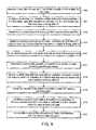
- FIGS. 1A , 1 B, 1 Cillustrate high level diagrams showing illustrative memory devices that allow for concurrent operations, in accordance with various aspects of the invention.
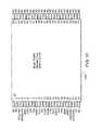
- FIG. 2Ais a high-level block diagram of an illustrative memory device in accordance with aspects of the invention.
- FIG. 2Cis a schematic of an input serial to parallel register block shown in FIG. 2A , according to an embodiment of the present invention.
- FIG. 2Dis a schematic of a path switch circuit shown in FIG. 2A , according to an embodiment of the present invention.
- FIG. 2Eis a schematic of an output parallel to serial register block shown in FIG. 2A , according to an embodiment of the present invention.
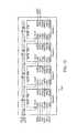
- FIGS. 3A , 4 , 5 A, 6 A, and 7illustrate timing diagrams for memory operations performed by a memory device in accordance with various aspects of the invention.
- FIGS. 3B , 5 B, and 6 Bare flowcharts illustrating the memory operations of FIGS. 3A , 5 A, and 6 A, respectively, in a memory device in accordance with various aspects of the invention.
- FIGS. 8A , 8 B, and 8 Cillustrate timing diagrams for concurrent memory operations performed in a memory device in accordance with various aspects of the invention.
- FIGS. 9 and 10are flowcharts diagramming a method of controlling data transfer between a plurality of serial data link interfaces and a plurality of memory banks in accordance with various aspects of the invention.
- FIG. 11illustrates a block diagram of the pin-out configuration of a memory device in accordance with various aspects of the invention.
- FIG. 13depicts a high-level block diagram of a cascaded configuration of numerous memory devices in accordance with various aspects of the invention.
- FIG. 14illustrates a simplified timing diagram for a memory operation performed on a memory device in a cascaded configuration in accordance with aspects of the invention.
- a serial data interface for a semiconductor memory having at least two memory banksis disclosed.
- the serial data interfacecan include one or more serial data links in communication with centralized control logic, where each serial data link can receive commands and data serially, and can provide output data serially.
- Each serial data linkcan access any memory bank in the memory for programming and reading of data.
- At least one advantage of a serial interfaceis a low-pin-count device with a standard pin-out that is the same from one density to another, thus, allowing compatible future upgrades to higher densities without board redesign.
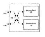
- FIGS. 1A and 1Bare high level diagrams showing illustrative memory devices that support concurrent operations, in accordance with various aspects of the invention.
- FIG. 1Ashows a memory device having multiple serial data link interfaces 102 and 104 and multiple memory banks 106 and 108 . The presently shown arrangement is referred to herein as a dual port configuration.
- Each serial data link interfacehas an associated input/output pin and data input and data output circuitry, which will be described in further detail with respect to FIG. 2A .
- serial data link interfaces 102 and 104 in the memory deviceare independent and can transfer data to and from any of the memory banks 106 and 108 .
- serial data link 102can transfer data to and from memory bank 106 or memory bank 108 .
- serial data link 104can transfer data to and from memory bank 106 and memory bank 108 . Since the two serial data link interfaces shown are independent, they can concurrently transfer data to and from separate memory banks.
- Linkrefers to the circuitry that provides a path for, and controls the transfer of, data to and from one or more memory banks.
- a control module 110is configurable with commands to control the exchange of data between each serial data link interface 102 and 104 and each memory bank 106 and 108 .
- control module 110can be configured to allow serial data link interface 102 to read data from memory bank 106 at the same time that serial data link interface 104 is writing data to memory bank 108 .
- This featureprovides enhanced flexibility for system design and enhanced device utilization (e.g., bus utilization and core utilization).
- control module 110can include control circuits, registers and switch circuits.
- FIG. 1Bshows an embodiment in which a single serial data link interface 120 is linked to multiple memory banks 122 and 124 via a control module 126 .
- This presently shown arrangementis referred to herein as a single port configuration, and utilizes less memory device input/output pins than the dual port configuration shown in FIG. 1A .
- Control module 126is configured to perform or execute two operating processes or threads, so that serial data link interface 120 can exchange data with memory banks 122 and 124 in a pipelined fashion. For example, while data is being written into memory bank 122 , data link interface 120 can be reading data out of memory bank 124 .
- the memory deviceemulates multiple link operations using a single link configuration with illustrated in FIG.
- any available bankcan be accessed while the other bank may be in a busy state.
- the memory devicecan achieve enhanced utilization of the single link configuration by accessing the other available bank through link arbitration circuitry.
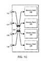
- FIGS. 1A and 1Binclude two memory banks for illustration purposes only.
- a single memory devicemay include, for example, 2, 4, or more memory banks.
- FIG. 1Cshows an embodiment in which four independent serial data links 132 , 134 , 136 and 138 are configured to exchange data with four memory banks 140 , 142 , 144 and 146 under the control of a control module 150 .
- With a virtual multiple link configurationonly one link is necessary, so the remaining links (e.g., in FIG. 1A dual link or FIG.
- 1C quad link pinout configurationsare not used and may be considered as NC (i.e., No Connection).
- NCi.e., No Connection
- At least one advantage of a serial data link interface compared to a conventional parallel interface structureis the reduced number of pins on the memory device while link flexibility and large density are maintained.
- a memory device in accordance with aspects of the inventionmay utilize fewer pins (e.g., 11 pins) on a single side of a standard package 1100 , as illustrated in FIG. 11 .
- a different and smaller type of packagecan be used instead, since there are less internal bond pads that are required.
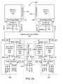
- FIG. 2Aillustrates a more detailed schematic diagram of the memory device shown in FIG. 1A , according to one embodiment of the present invention.
- the architecture of each memory bank in the memory device 200may be the same or similar to a NAND Flash memory core architecture.
- FIG. 2Aillustrates those circuits which are relevant to the invention, and intentionally omits certain circuit blocks to simplify FIG. 2A .
- memory device 200 implemented with a Flash memory core architecturewill include high voltage generator circuits that are necessary for programming and erasing the memory cells.
- Core architectureor core circuitry
- Memory device 200includes a multiplicity of identical memory banks with their respective data, control and addressing circuits, such as memory bank A 202 and memory bank B 204 , an address and data path switch circuit 206 connected to both memory banks 202 and 204 , and identical interface circuits 205 and 207 , associated with each memory bank for providing data to and for receiving data from the switch circuit 206 .
- Memory banks 202 and 204are preferably non-volatile memory, such as Flash memory, for example. Logically, the signals received and provided by memory bank 202 are designated with the letter “A”, while the signals received and provided by memory bank 204 are designated with the letter “B”.
- each interface circuit 205 / 207receives access data in a serial data stream, where the access data can include a command, address information and input data for programming operations, for example. In a read operation, the interface circuit will provide output data as a serial data stream in response to a read command and address data.
- the memory device 200further includes global circuits, such as a control interface 208 and status/ID register circuit 210 , which provide global signals such as clock signal sclki and reset to the circuits of both memory banks 202 and 204 and the respective interface circuits 205 and 207 .
- Memory bank 202includes well known memory peripheral circuits such as sense amplifier and page buffer circuit block 212 for providing output data DOUT_A and for receiving input program data DIN_A, and row decoder block 214 .
- block 212will also include column decoder circuits.
- a control and predecoder circuit block 216receives address signals and control signals via signal line ADDR_A, and provides predecoded address signals to the row decoders 214 and the sense amplifier and page buffer circuit block 212 .
- the peripheral circuits for memory bank 204are identical to those previously described for memory bank 202 .
- the circuits of memory bank Binclude a sense amplifier and page buffer circuit block 218 for providing output data DOUT_B and for receiving input program data DIN_B, a row decoder block 220 , and a control and predecoder circuit block 222 .
- Control and predecoder circuit block 222receives address signals and control signals via signal line ADDR_B, and provides predecoded address signals to the row decoders 220 and the sense amplifier and page buffer circuit block 222 .
- Each memory bank and its corresponding peripheral circuitscan be configured with well known architectures.
- each memory bankis responsive to a specific command and address, and if necessary, input data.
- memory bank 202will provide output data DOUT_A in response to a read command and a read address, and can program input data in response to a program command and a program address.
- Each memory bankcan be responsive to other commands such as an erase command, for example.
- path switch 206is a dual port circuit which can operate in one of two modes for passing signals between the memory banks 202 and 204 , and the interface circuits 205 and 207 .
- Firstis a direct transfer mode where the signals of memory bank 202 and interface circuit 205 are passed to each other. Concurrently, the signals of memory bank 204 and interface circuit 207 are passed to each other in the direct transfer mode.
- Secondis a cross-transfer mode where the signals of memory bank 202 and interface circuit 207 are passed to each other. At the same time, the signals of memory bank 204 and interface circuit 205 are passed to each other.
- a single port configuration of path switch 206will be discussed later.
- interface circuits 205 and 207receive and provide data as serial data streams. This is for reducing the pin-out requirements of the chip as well as to increase the overall signal throughput at high operating frequencies. Since the circuits of memory banks 202 and 204 are typically configured for parallel address and data, converting circuits are required.
- Interface circuit 205includes a serial data link 230 , input serial to parallel register block 232 , and output parallel to serial register block 234 .
- Serial data link 230receives serial input data SIP 0 , an input enable signal IPE 0 and an output enable signal OPE 0 , and provides serial output data SOP 0 , input enable echo signal IPEQ 0 and output enable echo signal OPEQ 0 .
- Signal SIP 0 (and SIP 1 )is a serial data stream which can each include address, command and input data.
- Serial data link 230provides buffered serial input data SER_IN 0 corresponding to SIP 0 and receives serial output data SER_OUT 0 from output parallel to serial register block 234 .
- the input serial-to-parallel register block 232receives SER_IN 0 and converts it into a parallel set of signals PAR_IN 0 .
- the output parallel-to-serial register block 234receives a parallel set of output data PAR_OUT 0 and converts it into the serial output data SER_OUT 0 , which is subsequently provided as data stream SOP 0 .
- Output parallel-to-serial register block 234can also receive data from status/ID register circuit 210 for outputting the data stored therein instead of the PAR_OUT 0 data. Further details of this particular feature will be discussed later.
- serial data link 230is configured to accommodate daisy chain cascading of the control signals and data signals with another memory device 200 .
- Serial interface circuit 207is identically configured to interface circuit 205 , and includes a serial data link 236 , input serial-to-parallel register block 240 , and output parallel-to-serial register block 238 .
- Serial data link 236receives serial input data SIP 1 , an input enable signal IPE 1 and an output enable signal OPE 1 , and provides serial output data SOP 1 , input enable echo signal IPEQ 1 and output enable echo signal OPEQ 1 .
- Serial data link 236provides buffered serial input data SER_IN 1 corresponding to SIP 1 and receives serial output data SER_OUT 1 from output parallel-to-serial register block 238 .
- the input serial-to-parallel register block 238receives SER_IN 1 and converts it into a parallel set of signals PAR_IN 1 .
- the output parallel-to-serial register block 240receives a parallel set of output data PAR_OUT 1 and converts it into the serial output data SER_OUT 1 , which is subsequently provided as data stream SOP 1 .
- Output parallel to serial register block 240can also receive data from status/ID register circuit 210 for outputting the data stored therein instead of the PAR_OUT 1 data.
- serial data link 236is configured to accommodate daisy chain cascading of the control signals and data signals with another memory device 200 .
- Control interface 208includes standard input buffer circuits, and generates internal chip select signal chip_sel, internal clock signal sclki, and internal reset signal reset, corresponding to CS#, SCLK and RST# respectively. While signal chip_sel is used primarily by serial data links 230 and 236 , reset and sclki are used by many of the circuits throughout memory device 200 .
- FIG. 2Bis a schematic of serial data link 230 , according to an embodiment of the invention.
- Serial data link 230includes input buffers 242 for receiving input signals OPE 0 , IPE 0 and SIP 0 , output drivers 244 for driving signals SOP 0 , IPEQ 0 and OPEQ 0 , flip-flop circuits 246 for clocking out signals out_en 0 and in_en 0 , inverter 248 and multiplexor (MUX) 250 .
- the input buffers for signals OPE 0 and SIP 0are enabled in response to chip_sel, and the output driver for signal SOP 0 is enabled in response to an inverted chip_sel via inverter 248 .
- Signal out_en 0enables an output buffer, which is shown later in FIG. 2E and provides signal SER_OUT 0 .
- Signal in_en 0enables the input serial to parallel register block 232 to latch SER_IN 0 data.
- Signals in_en 0 , out_en 0 and SER_IN 0are shown later in FIG. 2E and provides signal SER_OUT 0 .
- Serial data link 230includes circuits to enable daisy chain cascading of the memory device 200 with another memory device. More specifically, the serial input data stream SIP 0 , and enable signals OPE 0 and IPE 0 can be passed through to the corresponding pins of another memory device through serial data link 230 .
- SER_NOis received by AND logic gate 252 and passed to its corresponding flip-flop 246 when in_en 0 is at the active high logic level. Simultaneously, in_en 0 at the active high logic level will control MUX 250 to pass Si_next 0 to output driver 244 .
- IPE 0 and OPE 0can be clocked out to IPEQ 0 and OPEQ 0 through respective flip-flops 246 . While serial data link 230 has been described, it is noted that serial data link 240 includes the same components, which are interconnected in the same way as shown for serial data link 230 in FIG. 2B .
- FIG. 2Cis a schematic of the input serial to parallel register block 232 .
- This blockreceives the clock signal sclki, the enable signal in_en 0 and the input data stream SER_IN 0 , and converts SER_IN 0 into parallel groups of data.
- SER_IN 0can be converted to provide a command CMD_ 0 , a column address C_ADD 0 , a row address R_ADD 0 and input data DATA_IN 0 .
- the presently disclosed embodiment of the inventionpreferably operates at a high frequency, such as at 200 MHz for example. At this speed, the serial input data stream can be received at a rate faster than the received command can be decoded. It is for this reason that the serial input data stream is initially buffered in a set of registers. It should be understood that the presently shown schematic also applies to input serial to parallel register block 240 , where the only difference lies in the designator of the signal names.
- the input serial-to-parallel register block 232includes an input controller 254 for receiving in_en 0 and sclki, a command register 256 , a temporary register 258 , and a serial data register 260 . Since the data structure of the serial input data stream is predetermined, specific numbers of bits of the input data stream can be distributed to the aforementioned registers. For example, the bits corresponding to a command can be stored in the command register 256 , the bits corresponding to row and column addresses can be stored in the temporary register 258 , and the bits corresponding to input data can be stored in the serial data register 260 .
- the distribution of the bits of the serial input data streamcan be controlled by input controller 254 , which can include counters for generating the appropriate register enabling control signals after each predetermined number of bits have been received.
- input controller 254can include counters for generating the appropriate register enabling control signals after each predetermined number of bits have been received.
- each of the three registerscan be sequentially enabled to receive and store bits of data of the serial input data stream in accordance with the predetermined data structure of the serial input data stream.
- a command interpreter 262receives a command signal in parallel from command register 256 , and generates a decoded command CMD_ 0 .
- Command interpreter 262is a standard circuit implemented with interconnected logic gates or firmware, for decoding the received commands. As shown in FIG. 4 , CMD_ 0 can include signals cmd_status and cmd_id.
- a switch controller 264receives one or more signals from CMD_ 0 to control a simple switch circuit 266 . Switch circuit 266 receives all the data stored in the temporary register 258 in parallel, and loads one or both of column address register 268 and row/bank register 270 with data in accordance with the decoded command CMD_ 0 .
- This decodingis preferably done because the temporary register may not always include both column and row/bank address data.
- a serial input data stream having a block erase commandwill only use a row address, in which case only the relevant bits stored in the temporary register 258 are loaded into row/bank register 270 .
- the column address register 268provides parallel signal C_ADD 0
- the row/bank address register 270provides parallel signal R_ADD 0
- data register 272provides parallel signal DATA_IN 0 , for programming operations.
- CMD_ 0 , C_ADD 0 , R_ADD 0 and DATA_IN 0(optional), form the parallel signal PAR_IN 0 .
- Bit widths for each of the parallel signalshave not been specified, as the desired width is a design parameter which can be customized, or tailored to adhere to a particular standard.
- Table 1lists possible OP (operation) codes for CMD_ 0 and corresponding states of the column address (C_ADD 0 ), row/bank address (R_ADD 0 ), and the input data (DATA_IN 0 ).
- Table 2shows the preferred input sequence of the input data stream.
- the commands, addresses, and dataare serially shifted in and out of the memory device 200 , starting with the most significant bit.
- Command sequencesstart with a one-byte command code (“cmd” in Table 2).
- the one-byte command codemay be followed by column address bytes (“ca” in Table 2), row address bytes (“ra” in Table 2), bank address bytes (“ba” in Table 2), data bytes (“data” in Table 2), and/or a combination or none.
- FIG. 2Dis a schematic of path switch 206 shown in FIG. 2A .
- Switch 206is logically divided into two switch sub-circuits 274 and 276 , which are identically configured.
- Switch sub-circuit 274includes four input multiplexors 278 that selectively pass the commands, addresses and input data of either interface circuit 205 or interface circuit 207 to the circuits of memory bank 202 . These signals have been previously grouped in FIG. 2C as PAR_IN 0 by example.
- Switch sub-circuit 274includes one output multiplexor 280 for selectively passing the output data from either memory bank 202 or memory bank 204 to interface circuit 205 .
- Switch sub-circuit 276includes four input multiplexors (not shown) that selectively pass the commands, addresses and input data of either interface circuit 205 or interface circuit 207 to the circuits of memory bank 204 .
- Switch sub-circuit 276includes one output multiplexor (not shown) for selectively passing the output data from either memory bank 202 or memory bank 204 to interface circuit 207 .
- Both switch sub-circuits 274 and 276can simultaneously operate in the direct transfer mode or the cross-transfer mode, depending on the state of switch control signal SW_CONT.
- Path switch circuit 206is presently shown in a dual port configuration, meaning that both memory banks 202 and 204 can be simultaneously accessed through either interface circuits 205 and 207 .
- path switch 206can operate in a single port mode in which only one of interface circuits 205 and 207 is active. This configuration can further reduce the pin-out area requirements of the memory device 200 since the input/output pads associated with the unused interface circuit are no longer required.
- switch sub-circuits 274 and 276are set to operate in the direct transfer mode only, with the exception of the respective output multiplexors 280 which can remain responsive to the SW_CONT selection signal.
- a supplemental path switch(not shown) is included in the input parallel to serial register block 232 (or block 234 ), for selectively passing the data from the outputs of switch 266 and serial data register 260 to the corresponding column, row/bank and data registers of either input serial to parallel register block 232 or 240 .
- the supplemental path switchcan be similar to switch 206 .
- the column, row/bank and data registers of both input serial to parallel register blocks 232 and 240can be loaded with data for alternate memory bank accesses, or for substantially concurrent accesses.
- FIG. 2Eis a schematic of output parallel-to-serial register block 234 . It is noted that output parallel-to-serial register block 238 is identically configured. Output parallel-to-serial register block 234 provides either data accessed from the memory bank, or status data previously stored in registers. More specifically, the user or system can request a status of either serial data links 230 or 236 . A value of ‘1’ in a designated bit location (e.g., bit 4 ) in the outputted status data can indicate that the particular serial data link interface is busy. The fixed data can further include chip identification data, which with the status data, can both be pre-loaded with default states upon power up of the memory device 200 .
- chip identification datawhich with the status data
- the status datacan be configured to have any preselected bit pattern that is recognizable by the system.
- FIG. 2Ecan include additional control circuitry for updating one or more bits stored in register 284 , based on one or more predetermined conditions. For example, one or more status bits can be changed based on a count of elapsed clock cycles, or based on a combination of one or more flag signals received from various circuit blocks of memory device 200 .
- Output parallel to serial register block 234includes a first parallel-to-serial register 282 for receiving output data PAR_OUT 0 from path switch 206 , a second parallel-to-serial register 284 for receiving fixed data from a multiplexor 286 .
- Multiplexor 286selectively passes one of the status data stored in status register 288 or chip identification data stored in ID register 290 in response to signal cmd_id.
- An output multiplexor 292passes the data from either the first parallel-to-serial register 282 or the second parallel-to-serial register 284 in response to either cmd_id or cmd_status being active, via OR gate 294 .
- a serial output control circuit 296 enabled by out_en 0provides SER_OUT 0 .
- serial data link interface status indicatormay be joined with other types of status indicator (e.g., memory bank status indicator) and/or physically located outside the register block (e.g., in the link arbitration module or in the control module 238 ).
- the serial data link interface status indicatoris a one-bit register.
- FIGS. 3A , 4 , 5 A, 6 A, and 7illustrate example timing diagrams for some memory operations performed by memory device 200 in accordance with various aspects of the invention.
- Some memory commands performed by the memory device 200include, but are not limited to, page read, random data read, page read for copy, target address input for copy, serial data input, random data input, page program, block erase, read status, read ID, write configuration register, write device name entry, reset, and/or bank select.
- page readrandom data read
- page read for copytarget address input for copy
- serial data inputrandom data input
- page programblock erase
- read statusread ID
- write configuration registerwrite device name entry, reset, and/or bank select
- FIG. 3Ashows a simplified flowchart paralleling the operation of the “page read” memory command 314 in the timing diagram of FIG. 3A .
- FIG. 3Bshows a simplified flowchart paralleling the operation of the “page read” memory command 314 in the timing diagram of FIG. 3A .
- the steps illustrated in FIG. 3Bwill be discussed in conjunction with the timing diagram of FIG. 3A .
- a “page read” memory command 314is read in at serial data link 230 of the memory device 200 .
- the incoming data stream in this exampleis a six-byte serial data stream (i.e., serial input data) including command data (in the first byte), column address data (in the second and third bytes), and row and bank address data (in the fourth, fifth, and sixth bytes).
- the bank addresscan be used to determine access to either bank 202 or 204 via patch switch 206 .
- different memory commandsmay have a different data stream.
- a “random data read” memory commandhas a predetermined data stream of only three bytes: command data (in the first byte) and column address data (in the second and third bytes).
- the address field of the serial input dataonly contained column address data and was two bytes long. Meanwhile, in the former example, the address field was five bytes long.
- numerous memory commands and predetermined data streamsare apparent in accordance with various aspects of the invention.
- the serial input (SIPx) port 308is sampled on the first falling edge of the serial clock (SCLK) signal 304 (where ‘x’ acts as a placeholder representing the link interface number, e.g., link 0 interface 232 or link 1 interface 234 ).
- the data read out (in step 328 )is a data stream corresponding to a “page read” memory command 314 .
- the CS# signal 302is an input into the memory device 200 and may be used, among other things, to indicate whether the memory device 200 is active (e.g., when CS# is low) or whether the memory device's serial outputs are at high impedance (e.g., when CS# is high).
- the IPEx signal 306indicates whether an incoming data stream will be received at a particular link interface (e.g., when IPEx is high) or whether a particular link interface will ignore the incoming data stream (e.g., when IPEx is low). The incoming data stream is received at the memory device at the SIPx 308 of a link interface.
- the system clock (SCLK) signal 304is an input into the memory device 200 and is used to synchronize the various operations performed by the numerous circuits of the memory device 200 .
- SCLKsystem clock
- a memory device in accordance with various aspects of the inventionmay be synchronized with such a clock signal (e.g., operations and data transfers occur at the rising and/or falling edge of the clock signal) or may be asynchronous (i.e., not synchronous).
- input datais latched on the falling edge of SCLK and output data 322 appears on the serial output pin 312 SPOx after the rising edge of SCLK.
- the status of the “page read”can be checked on the SPOx pin 312 as shown in FIG.
- FIG. 3Aillustrates a “page read” with subsequent “read status”, a “page read” without a “read status” is also contemplated in accordance with aspects of the invention. In that embodiment, no data would be provided on the SPOx pin until output data would be ready.
- the command data sampled by SIPx 308is written to the appropriate register (e.g., command register 256 ) in FIG. 2C .
- the appropriate registere.g., command register 256
- At least one benefit to the option of designing the incoming data stream such that the first byte is command datais that the data can be transferred to the command register without additional processing.
- Subsequent bytes in the data streammay be address data and/or input data according to the type of memory command.
- the set of memory commands recognized by a memory device in accordance with various aspects of the inventionmay be defined by word-basis (i.e., 16 bits) or any I/O width. In FIG.
- the command data(i.e., 00h corresponding to “page read” 314 ) is followed by five bytes of address data: two bytes of column address data and three bytes of row/bank address data.
- the address datais written to an address register 258 in FIG. 2C .
- the address datais used to locate the data stored in the memory bank 202 that is to be read.
- the pre-decoder circuit 216 , column decoder in circuit 212 , and row decoder 214are utilized during this process to select the data to be read.
- the pre-decoder module 214is used to pre-decode the address information.
- the column decoder in circuit 212 and row decoder 214are used to activate the bitline and wordline corresponding to the address data.
- multiple bitlinesare activated corresponding to a wordline.
- the data stored in the memory bank 202is transferred to a page register in circuit 212 after being sensed by sense amplifiers.
- the data in the page registermay not be available until time 318 in FIG. 3A , i.e. the output pin SPOx will indicate “busy”.
- the amount of time lapsedis referred to as the transfer time (t R ).
- the transfer time periodends at time 318 (in FIG. 3A ) and lasts for a duration of t R .
- a memory bank status indicatoris set to indicate that the particular memory bank (e.g., memory bank 202 ) is “busy”.
- the illustrative memory bank status indicator of FIG. 3Ais a 1-byte field with one of the bits (e.g., bit 4 ) indicating whether memory bank 202 (i.e., bank 0 ) is “busy” or “ready”.
- the memory bank status indicatoris stored in a status register 288 of FIG. 2E .
- the memory bank status indicatoris updated (e.g., bit 4 is set to ‘0’) after a memory bank has been identified from the incoming data stream.
- the bank status indicatoris updated (e.g., bit 4 is set to ‘1’) to indicate that the memory bank is no longer “busy” (i.e., “ready”).
- the bank status indicatoras well as the SPOx output pin will indicate the “busy” status as will be explained in further detail below.
- FIG. 3Athe memory bank status indicator is depicted in FIG. 3A as a 1-byte field, its size is not necessarily so limited. At least one benefit of a larger status indicator is the ability to monitor the status of a greater quantity of memory banks.
- the status indicatormay be used to monitor other types of status (e.g., whether the memory bank is in a “pass” or “fail” status after a memory operation, such as a “page program”, was performed).
- the status indicator of this examplebeing implemented such that each bit designates the status of a different memory bank is exemplary only.
- the value of a combination of bitsmay be used to indicate the status of a memory bank (e.g., by using logic gates and other circuitry). The operation of the “read status” command corresponding to the memory bank status indicator is discussed in relation to FIG. 7 below.
- the memory bank status indicator in the example of FIG. 3Ais read using the “read status” memory command 316 (in step 328 ). Sometime during the transfer time period, a “read status” command 316 is sent to the command register in the register block 224 . The “read status” command instructs the memory device 200 to monitor the status of the memory bank 202 to determine when the transfer of data from the memory bank 202 to a page register 216 is complete. The “read status” command is sent from the control module 238 through the data path control module 230 or directly by the data path control module 230 .
- the output port enable (OPEx) signal 310is driven high and the contents of the memory bank status indicator are outputted through the serial output (SOPx) port 312 . Similar to the IPEx signal 306 , the OPEx signal 310 enables the serial output port buffer (e.g., the data output register) when set to high.
- the status indicator data in the SOPxindicates that the memory bank 202 has changed (in step 330 ) from a “busy” status to a “ready” status. The OPEx signal 310 is returned to low since the content of the status indicator is no longer needed.
- the IPEx signalis set high, and a “page read” command 320 with no trailing address data is re-issued (in step 332 ) to the command register in the register block 224 in order to provide data from the data registers to the output pin SPOx.
- the OPEx signalis set high (and IPEx is returned to low), and the contents of the page register 216 are transferred to the SOPx 312 .
- the output datais provided (in step 334 ) through the link interface 230 out of memory device 200 . Error correction circuitry (not shown in the Figures) can check the output data and indicate a read error if an error is detected.
- FIG. 3Ais merely one example of memory device operation in accordance with aspects of the invention, and the invention is not so limited.
- other memory commands and timing diagramsare envisioned in accordance with various aspects of the invention.
- FIG. 4a simplified timing diagram for the “random data read” command following a “page read” command is illustrated.
- the “random data read” commandenables the reading of additional data at a single or multiple column addresses subsequent to a “page read” command or a “random data read” command.
- the data stream for a “random data read” command 402is comprised of three bytes: command data (in the first byte) and column address data (in the second and third bytes). No row address data is required since data will be read from the same row selected in the “page read” command.
- a “random data read” command issued after a normal “page read” command has completedresults in some of the data 404 from the current page (i.e., the page read during the earlier command) being outputted. At least one benefit to the “random data read” command is the increased efficiency with which data from the preselected page may be outputted since the data is already present in a page register of circuit 212 corresponding to the memory bank 202 .
- FIG. 5Aa timing diagram for the “page program” command is illustrated. Since the embodiment illustrated in FIG. 2A utilizes a serial data input and output link structure, prior to beginning to program a page, the program data must first be loaded into a bank page register. This is accomplished with the “serial data input command”.
- the “serial data input” command 502is comprised of a serial data loading period during which up to a page (e.g., 2,112 bytes) of data is loaded into the page buffer in circuit 212 .
- a “page start” command 504is issued to transfer the data from the bank register into the appropriate memory bank.
- a “page start” commandis divided into two steps: serial data input and verification.
- the memory bank status indicatorwill provide a “pass” (as opposed to a “fail”) result to indicate a successful operation.
- the timing diagram and steps involving in the example of FIG. 5Aare similar to those of FIG. 3A , which was previously described in greater detail.
- FIG. 5Bshows a simplified flowchart paralleling the operation of the “page program” command in the timing diagram of FIG. 5A .
- the “serial data input” command 502is input to the serial input port (SIP) line.
- the data stream input to the SIP line in this exampleis a multi-byte serial data stream (i.e., serial input data) beginning with the command data (in the first byte).
- the column address data (in the second and third bytes of the serial data stream) and row address/bank dataare input (in step 508 ) to the SIP line.
- step 510the input data is input (in step 510 ) to the SIP line in the subsequent bytes of the serial data stream.
- step 512a “program start” command 504 is issued.
- step 514a “read status” command is written to the SIP line (in step 514 ). This results in the memory device monitoring the status bits of the memory bank status register. Once the status bits indicate that the memory bank is ready (in step 516 ) and that the memory bank indicates a “pass” (in step 518 ), then the “page program” memory command has been successfully performed.
- the “page read for copy” and “target address input for copy” memory commandsare others operations performed by a memory device in accordance with aspects of the invention. If the “page read for copy” command is written to the command register of a serial link interface, then the internal source address (in 3 bytes) of the memory location is written. Once the source address is inputted, the memory device transfers the contents of the memory bank at the specified source address into a data register. Subsequently, the “target address input for copy” memory command (with a 3-byte bank/row address sequence) is used to specify a target memory address for the page copy operation. A “page program” command may then be used to cause the internal control logic to automatically write the page data to the target address. A “read status” command can be subsequently used to confirm the successful execution of the command. Other memory operations will be apparent to one skilled in the art after review of the entire disclosure herein.
- FIG. 6Aa timing diagram for the “erase” (or “block erase”) command is illustrated.
- FIG. 6Bshows a simplified flowchart paralleling the operation of the “erase” command in the timing diagram of FIG. 6A .
- erasingtypically occurs at the block level.
- a Flash memory device 200can have, at each bank, 2,048 erasable blocks organized as 64 2,112-byte (2,048+64 bytes) pages per block. Each block is 132K bytes (128K+4K bytes).
- the “erase” commandoperates on one block at a time.
- Block erasingis started by writing command data 602 at step 610 corresponding to the “erase” command (i.e., command data of ‘60h’) to the command register via SIPx along with three bytes for row and bank addresses at step 612 .
- the internal erase state machineautomatically executes the proper algorithm and controls all the necessary timing to erase and verify the operation.
- the “erase” operationmay be executed by writing or programming a logic value of ‘1’ to every memory location in a block of memory.
- the “read status” command 604(e.g., command data corresponding 70h) may be issued at step 614 .
- the appropriate bit (e.g., bit 4 ) of the memory bank status registerreflects the state (e.g., busy or ready) of the corresponding memory bank.
- the appropriate bit (e.g., bit 0 ) of the memory bank status registeris checked at step 620 to determine if the erase operation passed (i.e., successfully performed) at step 622 or failed at step 624 .
- the timing diagram and steps involving in the example of FIG. 6Aare similar to those of FIG. 3A , which was previously described in greater detail.
- the memory bank status indicatoris read using the “read status” memory command.
- a “read status” commandi.e., ‘70h’
- the memory device 200is instructed to monitor the status of the memory bank 202 to, among other things, determine when the transfer of data from the memory bank 202 to the page buffer in circuit 212 is successfully completed.
- the output port enable (OPEx) signalis driven high and the contents of the memory bank status indicator are outputted at 704 through the serial output (SOPx) port.
- the OPEx signalenables the serial output port buffer (e.g., the data output register) when set to high.
- the memory bank status indicatoris a 1-byte (i.e., 8-bit) field with each bit indicating, among other things, whether a memory bank (e.g., memory bank 202 ) is “busy” or “ready” and/or whether a operation performed on a memory bank (e.g., “erase” command) is has “passed” or “failed”.
- a memory banke.g., memory bank 202
- a operation performed on a memory banke.g., “erase” command
- At least one benefit of a larger status indicatoris the ability to monitor the status of a greater quantity of memory banks.
- the status indicator of this examplewas implemented such that each bit designated the status of a different memory bank, the invention is not so limited.
- the value of a combination of bitsmay be used to indicate the status of a memory bank (e.g., by using logic gates and other circuitry).
- FIGS. 8A , 8 B, and 8 Cillustrate timing diagrams for a memory device in accordance with aspects of the invention being used to perform concurrent operations using dual independent serial data links 230 and 236 .
- Some concurrent operations performed by a memory device in accordance with aspects of the inventioninclude, but are not limited to, concurrent read, concurrent program, concurrent erase, read while program, read while erase, and program while erase.
- FIG. 8Aillustrates a concurrent “page read” operation being performed on bank A (bank 202 ) and bank B (bank 204 ). In FIG. 8A , bank A is represented as “bank 0 ” while bank B is represented as “bank 1 ”. FIG. 8B .
- Other concurrent operationswill become apparent to one skilled in the art upon review of the entire disclosure herein.
- concurrent “page read” operations 802 , 804 directed at different memory banks in a memory device 200are executed.
- a “page read” command 804is issued through data link interface 236 (i.e., link 1 ) while a “page read” 802 is pending through data link interface 230 (i.e., link 0 ).
- FIG. 8Ashows the “page read” on bank 0 starting before the “page read” on bank 1 , the two “page read” operations can begin substantially simultaneously and operate concurrently.
- the outputted data 806 , 808 from each of the “page read” commandsis simultaneously sent through their respective data link interfaces. Therefore, each data link interface in memory device 200 may access any of the memory banks and operate independently. At least one benefit of this feature is greater flexibility in system design and an enhancement on device utilization (e.g., bus utilization and core utilization).
- the path of the outputted data from the memory bank to the data link interface in FIG. 8Ais similar to that of FIG. 3A discussed earlier.
- the outputted data from memory bank 204flows from S/A and page buffer 218 through path switch 206 controlled by a bank address for example, to output parallel-to-serial register block 240 , and to serial data link interface 236 (i.e., link 1 ).
- serial data link interface 236i.e., link 1 .
- the simultaneous data transfer between memory banks 202 and 204 and serial data link interfaces 230 , 236 , respectively,will occur independently of each other.
- serial data link interface 236can access bank 202 instead.
- the number of data link interfaces in memory device 200is not limited to the number of ports or pins on memory device 200 .
- the number of link interfaces in memory device 200limited by the number of memory banks in the memory device.
- each data link interfacemay process a single input stream and/or a single output stream.
- FIG. 8Billustrates a timing diagram of a “page read” command 810 and a “page program” command 812 directed at different memory banks in a memory device 200 being performed concurrently.
- a read operation(“page read” 810 ) is being performed in one of the plurality of memory banks (e.g., memory bank 202 ) through serial data link interface 230 .
- a write operation(“page program” 812 ) is being performed in another of the plurality of memory banks (e.g., memory bank 204 ) through serial data link interface 236 .
- each link in the memory device 200may access any of the memory banks and operate independently.
- FIG. 8Cis an illustrative timing diagram of a memory device 200 with two serial data link interfaces and two memory banks performing concurrent memory operations.
- an “erase” command 814 directed at memory bank 0 (bank 202 )is issued from serial interface link 0 (serial data link 230 ). While link 0 (serial data link 230 ) and memory bank 0 (bank 202 ) are busy with the “erase” command 814 , a “page program” command is received at the memory device and directed to use link 1 (serial data link 236 ). Thus, a “page program” command 816 is performed on memory bank 0 (bank 202 ) from serial data link interface 1 (serial data link 236 ).
- serial data interface 0serial data link 230
- Datais transferred between serial data link interface 0 (serial data link 230 ) and bank 0 (bank 202 ) during memory command 814 and between the same link interface 0 (serial data link 230 ) and bank 1 (bank 204 ) during memory command 818 . Therefore, in accordance with aspects of the invention, each link in the memory device 200 independently accesses any of the memory banks (i.e., memory banks that are not busy).
- FIGS. 8A , 8 B, and 8 Cillustrate merely some examples of concurrent memory operations envisioned in accordance with the invention.
- Other examples of concurrent operationsinclude, but are not limited to, concurrent erase, read while program, read while erase, program while erase, erase while program, and/or concurrent program.
- concurrent erase, read while program, read while erase, program while erase, erase while program, and/or concurrent programinclude, but are not limited to, concurrent erase, read while program, read while erase, program while erase, erase while program, and/or concurrent program.
- read and program commandscan be issued with or without read status commands.
- FIG. 9shows a more general description of two concurrent write operations between a plurality of serial link interfaces and a plurality of memory banks in accordance with aspects of the invention.
- FIG. 9illustrates a method of writing data via a serial data link interface to a memory bank in accordance with an embodiment of the invention.
- a data streamis received at a serial data link interface.
- the data streamcontains command, address and data that will be stored in registers.
- a serial data link interface status indicator corresponding to the first serial data link interfaceis updated to indicate that the first serial data link interface is being utilized.
- Step 904includes changing a bit value in the status register. The update in step 904 indicates that the particular interface is being utilized.
- step 906the data stream is parsed to extract a first memory bank identifier.
- the memory bank identifieruniquely identifies a memory bank in the memory device.
- the memory bank identifiermay be included within an address field or other field of the data stream.
- step 908a corresponding memory bank status indicator is updated.
- the updating occurring in steps 904 and 908can be driven by control signals generated by control circuits within status/ID register 210 for example. These control signals have been omitted from the included timing diagrams for simplicity.
- step 910the data is routed between the first serial data link and the first memory bank. It should be noted that step 910 has been simplified in this general description, since data is first written to a memory bank page register and then subsequently programmed into the memory bank.
- a second memory operationis concurrently performed using a second data stream that is routed between a second serial data link interface and a second memory bank.
- First a second data streamis received at a second one of the plurality of serial data link interfaces in step 912 .
- the serial data link interfaces referred to in steps 912 and 902are all part of the same memory device.
- step 914a serial data link interface status indicator corresponding to the second data link interface is updated to indicate that the second serial data link interface is being utilized.
- the second data streamis parsed to extract a second memory bank identifier in step 916 .
- a memory bank status indicator corresponding to the second memory bank identifieris updated to indicate that the second memory bank is being utilized in step 918 and in step 920 data is routed between the second serial data link interface and the second memory bank via the second memory bank's associated page register, as previously described in relation to the “page program” command.
- the serial data link interface indicator corresponding to each serial data link interfacewill be reset to indicate that the associated link is now available, while the memory bank indicator will remain busy until all associated data has been programmed, after which the memory bank indicator will indicate that the associated bank has become available.
- FIG. 10comprises illustrative steps that may be performed when data is read from a memory bank concurrently with the writing of data shown in steps 902 to 910 in FIG. 9 (designated as steps 1010 ).
- FIG. 10illustrates an example of some of the steps that may be performed in completing the concurrent memory operations diagrammed in FIG. 7 .
- a read request for data stored in a second memory bankis received from a second one of the plurality of serial data link interfaces.
- a serial data link interface status indicator corresponding to the second data link interfaceis updated to indicate that the second serial data link interface is being utilized.
- a memory bank status indicator corresponding to the second memory bank identifieris updated to indicate that the second memory bank is being utilized in step 1006 .
- step 1008data is routed between the second memory bank and the second serial data link interface.
- One or more of the steps shown in FIG. 10may be performed concurrently.
- FIG. 1Bthe memory device shown includes a single data link interface 120 configuration that uses a virtual multiple link.
- FIG. 1Bcan be implemented with the configuration of the input serial to parallel register 232 that has been previously described. More generally, the embodiment of FIG. 1B can be implemented with the memory device 200 , but with only one of the two serial data links being used. In conventional flash memory, I/O pins are occupied until an operation is complete. Therefore, no operation can be asserted during device busy status, which reduces device availability and decreases overall performance. In the example depicted in FIG. 1B , any available memory bank checked by a “read status” operation can be accessed after an operation has been initiated in one of the two memory banks.
- the memory devicecan utilize the serial data link to access available memory banks through the supplemental switch circuit. Therefore, in accordance with this aspect of the invention, a single link may be used to access multiple memory banks.
- This virtual multiple link configurationemulates multiple link operations using a single link.
- FIG. 12illustrates a timing diagram of a memory device with two memory banks performing memory operations using a virtual multiple link configuration in which a “page program” in bank 0 and a “page read” in bank 1 are to be executed.
- a “page program” command 1202 directed at memory bank 0is issued.
- the “page program” commandhas already been described earlier, but to recap, the “serial data input” command is first performed to load into the bank 0 page register the data to be programmed to bank 0 . Subsequently, a “page program command is issued and the data is written from the page register into bank 0 .
- a “read status” command 1204is issued device, the device indicates 1206 that bank 1 is “ready” (and that bank 0 is “busy”).
- a “page read” command 1208 directed at memory bank 1can be and is issued while memory bank 0 is busy.
- the “page read” commandhas been previously described.
- a “read status” command 1210can be (and in FIG. 12 is shown to be) issued to determine the status of the memory banks.
- the result of the “read status” commandindicates during interval 1212 that both memory bank 0 and memory bank 1 are ready.
- a “page read” command 1214(for bank 1 ) is issued that results in the contents of the memory address corresponding to the bank 1 “page read” command to be outputted on the serial output pin (SOP).
- the serial data interface link pin SIPis available to receive the “read status” command which identifies bank 1 as “ready”. Similarly, once the “page read” command on bank 1 has been initiated, the SIP pin is again available for a “read status” command, indicating that both banks 0 and 1 are now ready. As a result, the single serial data interface link can be used to access and check the status of both banks. Aspects of the virtual multiple link feature implemented in FIG. 12 illustrate that the link is available even while an earlier memory operation is pending. At least one benefit arising from this feature is the reduced pin count resulting from the virtual multiple link configuration. Another benefit is the increased performance of the memory device.
- aspects of the virtual multiple link featureare implemented with memory devices with dual or quad-link configurations, it may be desirable to consider all but one of the links as being inactive. For example, three of the four links in a quad-link configuration (in FIG. 1C ) may not be used and may be designated as NC (no connection). At least one benefit of such an implementation is a reduction in the number of pins on the memory device while maintaining link flexibility and availability.
- FIG. 13illustrates a daisy-chain cascade configuration 1300 for serially connecting multiple memory devices 200 .
- Device 0is comprised of a plurality of data input ports (SIP 0 , SIP 1 ), a plurality of data output ports (SOP 0 , SOP 1 ), a plurality of control input ports (IPE 0 , IPE 1 ), and a plurality of control output ports (OPE 0 , OPE 1 ).
- SIP 0 , SIP 1data input ports
- SOP 0 , SOP 1data output ports
- IPE 0 , IPE 1control input ports
- OPE 1control output ports
- a second flash memory devicemay be comprised of the same types of ports as Device 0 .
- Device 1may be serially connected to Device 0 .
- Device 1can receive data and control signals from Device 0 .
- One or more additional devicesmay also be serially connected alongside Device 0 and Device 1 in a similar manner.
- the final devicee.g., Device 3 in the cascade configuration provides data and control signals back to the memory controller after a predetermined latency.
- Each memory device 200(e.g., device 0 , 1 , 2 , 3 ) outputs an echo (IPEQ 0 , IPEQ 1 , OPEQ 0 , OPEQ 1 ) of IPE 0 , IPE 1 , OPE 0 , and OPE 1 (i.e., control output ports) to the subsequent device.
- the previously described circuits in FIG. 2Billustrate how the signals can be passed from one device to a subsequent daisy chained device.
- a single clock signalis communicated to each of the plurality of serially connected memory devices.
- FIG. 14depicts a highly-simplified timing diagram for a “page read” memory command 1402 received at memory device 1300 and directed at a memory bank in Device 2 in memory device 1300 .
- the memory commandis received at memory device 1300 and sent through Device 0 and Device 1 to Device 2 .
- the data stream corresponding to the “page read” command 1402will be transferred from the SIP 0 line of Device 0 in memory device 1300 through the circuitry of Device 0 and outputted at the SOP 0 line of Device 0 .
- the output of Device 0is reflected in the simplified timing diagram in FIG. 14 on the SOPx_D 0 output line at 1404 .
- “SOPx_D 0 ”corresponds to serial output port 0 on Device 0 .
- the data streamis subsequently received at SIPx_D 1 on Device 1 (at 1406 ) and sent through Device 1 to be outputted by Device 1 on the SOPx_D 1 line at 1408 .
- the data streamis received at SIPx_D 2 on Device 2 at 1410 .
- the circuitry in Device 2since the “page read” command is directed to a memory bank in Device 2 , in a manner similar to that described for the circuitry in memory device 200 , the circuitry in Device 2 receives the “page read” command and controls the transfer of the requested data from a memory bank in Device 2 to the SOPx_D 2 output line on Device 2 at 1412 .
- the data outputted by Device 2is received at Device 3 at 1414 and transferred through Device 3 and outputted from memory device 1300 .
- One skilled in the artwill recognize from the simplified timing diagram of FIG. 14 that a predetermined latency of four clock cycles resulted due to the cascading configuration.
- the incoming data stream in a cascaded device 1300is similar to that of a non-cascaded memory device 200 , however, the first byte of the data stream may be preceded by a one-byte device identifier. For example, a value of “0000” in the first byte may indicate Device 0 , while a value of “0001” may indicate Device 1 .
- the device identifierneed not necessarily be limited to one byte, but may be increased or decreased as desired.
- the device identifierneed not necessarily be positioned as the first byte in a data stream. For example, the size of the identifier may be increased to accommodate more devices in a cascaded configuration and be positioned with the address field of the data stream.
- the memory device 200uses a single monolithic 4 Gb chip. In another embodiment, the memory device uses a pair of stacked chips for 8 Gb. In yet another embodiment, the memory device 1300 uses a stack of four chips to make up 16 Gb.
- a flash memory device in accordance with various aspects of the inventionmay be an improved solution for large nonvolatile storage applications such as solid state file storage and other portable applications desiring non-volatility.
- the memory device 1300may benefit from a novel flash device cascade scheme for virtually unlimited number of linked devices to accommodate system integration with greater expandability and flexibility.
- the serial interfacewill provide additional performance improvement with higher clock rate, better signal integrity and lower power consumption.
- the serial interfacealso provides unlimited expandable I/O width without changing package configuration.
- the one-side pad architecture of a memory device in accordance with the inventionwith fewer number of I/O, greatly reduces chip package size.
- the memory devicescan be dual-bank memories, where each bank can be accessed by any serial link.
- the serial interface of the memory devicegreatly improves data throughput over traditional parallel interface schemes, while supporting feature-rich operations.
- a program operationcan be performed in 200 ⁇ s on a (2 K+64) byte page and an erase operation can be performed in 1.5 ms on a (128K+4K) byte block.
- An on-chip write controllermay be used to automate all program and erase functions including pulse repetition, where used, and internal verification and margining of data.
- ECCError Correcting Code
- real time mapping-out algorithmmay be used to enhance the extended reliability of 100K program/erase cycles in the memory device.
Landscapes
- Engineering & Computer Science (AREA)
- Theoretical Computer Science (AREA)
- Physics & Mathematics (AREA)
- General Engineering & Computer Science (AREA)
- General Physics & Mathematics (AREA)
- Human Computer Interaction (AREA)
- Microelectronics & Electronic Packaging (AREA)
- Read Only Memory (AREA)
- Dram (AREA)
- Information Transfer Systems (AREA)
Abstract
Description
| TABLE 1 |
| Command Set |
| Column | Row/Bank | Input Data | ||
| OP Code | Address | Address | (1 Byte to | |
| Operation | (1 Byte) | (2 Bytes) | (3 Bytes) | 2112 Bytes) |
| 00h | Valid | Valid | — | |
| Random Data Read | 05h | Valid | — | — |
| Page Read for Copy | 35h | — | Valid | — |
| Target Address Input for Copy | 8Fh | — | Valid | — |
| 80h | Valid | Valid | Valid | |
| Random Data Input | 85h | Valid | — | |
| Page Program | ||||
| 10h | — | — | — | |
| Block Erase | 60h | — | Valid | — |
| 70h | — | — | — | |
| Read ID | 90h | — | — | — |
| Write Configuration Register | A0h | — | — | Valid (1 Byte) |
| Write DN (Device Name) Entry | B0h | — | — | — |
| Reset | FFh | — | — | — |
| Bank Select | 20h | — | Valid (Bank) | — |
| TABLE 2 |
| Input Sequence in |
| 1st | 2nd | 3rd | 4th | 5th | 6th | 7th | 2115th | 2118th | |||
| Operation | Byte | Byte | Byte | Byte | Byte | Byte | Byte | . . . | Byte | . . . | Byte |
| Page Read | cmd | ca | Ca | ba/ra | ra | ra | — | — | — | — | — |
| Random Data | cmd | ca | Ca | — | — | — | — | — | — | — | — |
| Read | |||||||||||
| Page Read for | cmd | ba/ra | Ra | ra | — | — | — | — | — | — | — |
| Copy | |||||||||||
| Target Address | cmd | ba/ra | Ra | ra | — | — | — | — | — | — | — |
| Input for Copy | |||||||||||
| Serial Data | cmd | ca | Ca | ba/ra | ra | ra | data | . . . | data | . . . | data |
| Input | |||||||||||
| Random Data | cmd | ca | Ca | data | data | data | data | . . . | data | — | — |
| Input | |||||||||||
| Page Program | cmd | — | — | — | — | — | — | — | — | — | — |
| Block Erase | cmd | ba/ra | Ra | ra | — | — | — | — | — | — | — |
| Read Status | cmd | — | — | — | — | — | — | — | — | — | — |
| Read ID | cmd | — | — | — | — | — | — | — | — | — | — |
| Write | cmd | data | — | — | — | — | — | — | — | — | — |
| Configuration | |||||||||||
| Register | |||||||||||
| Write DN Entry | cmd | — | — | — | — | — | — | — | — | — | — |
| Reset | cmd | — | — | — | — | — | — | — | — | — | — |
| Bank Select | cmd | ba | — | — | — | — | — | — | — | — | — |
Claims (19)
Priority Applications (6)
| Application Number | Priority Date | Filing Date | Title |
|---|---|---|---|
| US12/732,745US8000144B2 (en) | 2005-09-30 | 2010-03-26 | Method and system for accessing a flash memory device |
| US13/171,667US8743610B2 (en) | 2005-09-30 | 2011-06-29 | Method and system for accessing a flash memory device |
| US13/790,361US9230654B2 (en) | 2005-09-30 | 2013-03-08 | Method and system for accessing a flash memory device |
| US14/964,958US9490014B2 (en) | 2005-09-30 | 2015-12-10 | Method and system for accessing a flash memory device |
| US15/273,122US9836227B2 (en) | 2005-09-30 | 2016-09-22 | Method and system for accessing a flash memory device |
| US15/807,720US10223003B2 (en) | 2005-09-30 | 2017-11-09 | Method and system for accessing a flash memory device |
Applications Claiming Priority (4)
| Application Number | Priority Date | Filing Date | Title |
|---|---|---|---|
| US72236805P | 2005-09-30 | 2005-09-30 | |
| US11/324,023US7652922B2 (en) | 2005-09-30 | 2005-12-30 | Multiple independent serial link memory |
| US12/179,835US7719892B2 (en) | 2005-09-30 | 2008-07-25 | Flash memory device with data output control |
| US12/732,745US8000144B2 (en) | 2005-09-30 | 2010-03-26 | Method and system for accessing a flash memory device |
Related Parent Applications (1)
| Application Number | Title | Priority Date | Filing Date |
|---|---|---|---|
| US12/179,835DivisionUS7719892B2 (en) | 2005-09-30 | 2008-07-25 | Flash memory device with data output control |
Related Child Applications (1)
| Application Number | Title | Priority Date | Filing Date |
|---|---|---|---|
| US13/171,667ContinuationUS8743610B2 (en) | 2005-09-30 | 2011-06-29 | Method and system for accessing a flash memory device |
Publications (2)
| Publication Number | Publication Date |
|---|---|
| US20100182838A1 US20100182838A1 (en) | 2010-07-22 |
| US8000144B2true US8000144B2 (en) | 2011-08-16 |
Family
ID=37899329
Family Applications (8)
| Application Number | Title | Priority Date | Filing Date |
|---|---|---|---|
| US11/324,023Active2027-07-31US7652922B2 (en) | 2005-09-30 | 2005-12-30 | Multiple independent serial link memory |
| US12/179,835ActiveUS7719892B2 (en) | 2005-09-30 | 2008-07-25 | Flash memory device with data output control |
| US12/732,745ActiveUS8000144B2 (en) | 2005-09-30 | 2010-03-26 | Method and system for accessing a flash memory device |
| US13/171,667ActiveUS8743610B2 (en) | 2005-09-30 | 2011-06-29 | Method and system for accessing a flash memory device |
| US13/790,361ActiveUS9230654B2 (en) | 2005-09-30 | 2013-03-08 | Method and system for accessing a flash memory device |
| US14/964,958ActiveUS9490014B2 (en) | 2005-09-30 | 2015-12-10 | Method and system for accessing a flash memory device |
| US15/273,122ActiveUS9836227B2 (en) | 2005-09-30 | 2016-09-22 | Method and system for accessing a flash memory device |
| US15/807,720ActiveUS10223003B2 (en) | 2005-09-30 | 2017-11-09 | Method and system for accessing a flash memory device |
Family Applications Before (2)
| Application Number | Title | Priority Date | Filing Date |
|---|---|---|---|
| US11/324,023Active2027-07-31US7652922B2 (en) | 2005-09-30 | 2005-12-30 | Multiple independent serial link memory |
| US12/179,835ActiveUS7719892B2 (en) | 2005-09-30 | 2008-07-25 | Flash memory device with data output control |
Family Applications After (5)
| Application Number | Title | Priority Date | Filing Date |
|---|---|---|---|
| US13/171,667ActiveUS8743610B2 (en) | 2005-09-30 | 2011-06-29 | Method and system for accessing a flash memory device |
| US13/790,361ActiveUS9230654B2 (en) | 2005-09-30 | 2013-03-08 | Method and system for accessing a flash memory device |
| US14/964,958ActiveUS9490014B2 (en) | 2005-09-30 | 2015-12-10 | Method and system for accessing a flash memory device |
| US15/273,122ActiveUS9836227B2 (en) | 2005-09-30 | 2016-09-22 | Method and system for accessing a flash memory device |
| US15/807,720ActiveUS10223003B2 (en) | 2005-09-30 | 2017-11-09 | Method and system for accessing a flash memory device |
Country Status (10)
| Country | Link |
|---|---|
| US (8) | US7652922B2 (en) |
| EP (3) | EP2306461A3 (en) |
| JP (4) | JP2009510656A (en) |
| KR (1) | KR101154148B1 (en) |
| CN (2) | CN104599698A (en) |
| AT (1) | ATE533158T1 (en) |
| CA (1) | CA2623747C (en) |
| HK (1) | HK1202974A1 (en) |
| TW (2) | TWI449048B (en) |
| WO (1) | WO2007036047A1 (en) |
Cited By (10)
| Publication number | Priority date | Publication date | Assignee | Title |
|---|---|---|---|---|
| US8427897B2 (en) | 2005-09-30 | 2013-04-23 | Mosaid Technologies Incorporated | Memory with output control |
| US8743610B2 (en) | 2005-09-30 | 2014-06-03 | Conversant Intellectual Property Management Inc. | Method and system for accessing a flash memory device |
| US9805802B2 (en) | 2015-09-14 | 2017-10-31 | Samsung Electronics Co., Ltd. | Memory device, memory module, and memory system |
| US10216655B2 (en) | 2016-03-02 | 2019-02-26 | Electronics And Telecommunications Research Institute | Memory expansion apparatus includes CPU-side protocol processor connected through parallel interface to memory-side protocol processor connected through serial link |
| US10445229B1 (en) | 2013-01-28 | 2019-10-15 | Radian Memory Systems, Inc. | Memory controller with at least one address segment defined for which data is striped across flash memory dies, with a common address offset being used to obtain physical addresses for the data in each of the dies |
| US10552085B1 (en) | 2014-09-09 | 2020-02-04 | Radian Memory Systems, Inc. | Techniques for directed data migration |
| US10552058B1 (en) | 2015-07-17 | 2020-02-04 | Radian Memory Systems, Inc. | Techniques for delegating data processing to a cooperative memory controller |
| US10642505B1 (en) | 2013-01-28 | 2020-05-05 | Radian Memory Systems, Inc. | Techniques for data migration based on per-data metrics and memory degradation |
| US10642748B1 (en) | 2014-09-09 | 2020-05-05 | Radian Memory Systems, Inc. | Memory controller for flash memory with zones configured on die bounaries and with separate spare management per zone |
| US10838853B1 (en) | 2013-01-28 | 2020-11-17 | Radian Memory Systems, Inc. | Nonvolatile memory controller that defers maintenance to host-commanded window |
Families Citing this family (218)
| Publication number | Priority date | Publication date | Assignee | Title |
|---|---|---|---|---|
| US7475174B2 (en)* | 2004-03-17 | 2009-01-06 | Super Talent Electronics, Inc. | Flash / phase-change memory in multi-ring topology using serial-link packet interface |
| KR100697270B1 (en)* | 2004-12-10 | 2007-03-21 | 삼성전자주식회사 | Low power multichip semiconductor memory device and its chip enable method |
| US11948629B2 (en) | 2005-09-30 | 2024-04-02 | Mosaid Technologies Incorporated | Non-volatile memory device with concurrent bank operations |
| US20070076502A1 (en) | 2005-09-30 | 2007-04-05 | Pyeon Hong B | Daisy chain cascading devices |
| US20070165457A1 (en) | 2005-09-30 | 2007-07-19 | Jin-Ki Kim | Nonvolatile memory system |
| US7747833B2 (en) | 2005-09-30 | 2010-06-29 | Mosaid Technologies Incorporated | Independent link and bank selection |
| US8364861B2 (en)* | 2006-03-28 | 2013-01-29 | Mosaid Technologies Incorporated | Asynchronous ID generation |
| US8335868B2 (en)* | 2006-03-28 | 2012-12-18 | Mosaid Technologies Incorporated | Apparatus and method for establishing device identifiers for serially interconnected devices |
| KR100843707B1 (en)* | 2006-05-11 | 2008-07-04 | 삼성전자주식회사 | Semiconductor memory device having data input / output port, memory module and memory system using same |
| US7904639B2 (en) | 2006-08-22 | 2011-03-08 | Mosaid Technologies Incorporated | Modular command structure for memory and memory system |
| US8407395B2 (en)* | 2006-08-22 | 2013-03-26 | Mosaid Technologies Incorporated | Scalable memory system |
| EP2487794A3 (en) | 2006-08-22 | 2013-02-13 | Mosaid Technologies Incorporated | Modular command structure for memory and memory system |
| US8700818B2 (en)* | 2006-09-29 | 2014-04-15 | Mosaid Technologies Incorporated | Packet based ID generation for serially interconnected devices |
| US8001441B2 (en)* | 2006-11-03 | 2011-08-16 | Sandisk Technologies Inc. | Nonvolatile memory with modulated error correction coding |
| US7817470B2 (en)* | 2006-11-27 | 2010-10-19 | Mosaid Technologies Incorporated | Non-volatile memory serial core architecture |
| US8019938B2 (en) | 2006-12-06 | 2011-09-13 | Fusion-I0, Inc. | Apparatus, system, and method for solid-state storage as cache for high-capacity, non-volatile storage |
| US7925854B2 (en)* | 2006-12-06 | 2011-04-12 | Mosaid Technologies Incorporated | System and method of operating memory devices of mixed type |
| US9116823B2 (en) | 2006-12-06 | 2015-08-25 | Intelligent Intellectual Property Holdings 2 Llc | Systems and methods for adaptive error-correction coding |
| US8433874B2 (en)* | 2006-12-06 | 2013-04-30 | Mosaid Technologies Incorporated | Address assignment and type recognition of serially interconnected memory devices of mixed type |
| US7752364B2 (en)* | 2006-12-06 | 2010-07-06 | Mosaid Technologies Incorporated | Apparatus and method for communicating with semiconductor devices of a serial interconnection |
| US9495241B2 (en) | 2006-12-06 | 2016-11-15 | Longitude Enterprise Flash S.A.R.L. | Systems and methods for adaptive data storage |
| US7554855B2 (en)* | 2006-12-20 | 2009-06-30 | Mosaid Technologies Incorporated | Hybrid solid-state memory system having volatile and non-volatile memory |
| US7613049B2 (en) | 2007-01-08 | 2009-11-03 | Macronix International Co., Ltd | Method and system for a serial peripheral interface |
| CN101617371B (en) | 2007-02-16 | 2014-03-26 | 莫塞德技术公司 | Non-volatile semiconductor memory with multiple external power supplies |
| US8122202B2 (en) | 2007-02-16 | 2012-02-21 | Peter Gillingham | Reduced pin count interface |
| WO2008101316A1 (en) | 2007-02-22 | 2008-08-28 | Mosaid Technologies Incorporated | Apparatus and method for using a page buffer of a memory device as a temporary cache |
| US8086785B2 (en) | 2007-02-22 | 2011-12-27 | Mosaid Technologies Incorporated | System and method of page buffer operation for memory devices |
| US7865756B2 (en)* | 2007-03-12 | 2011-01-04 | Mosaid Technologies Incorporated | Methods and apparatus for clock signal synchronization in a configuration of series-connected semiconductor devices |
| US7778074B2 (en)* | 2007-03-23 | 2010-08-17 | Sigmatel, Inc. | System and method to control one time programmable memory |
| TW200901042A (en)* | 2007-06-23 | 2009-01-01 | Jmicron Technology Corp | Storage device and circuit element switching method thereof |
| US7688652B2 (en)* | 2007-07-18 | 2010-03-30 | Mosaid Technologies Incorporated | Storage of data in memory via packet strobing |
| US7889578B2 (en)* | 2007-10-17 | 2011-02-15 | Mosaid Technologies Incorporated | Single-strobe operation of memory devices |
| WO2009062280A1 (en)* | 2007-11-15 | 2009-05-22 | Mosaid Technologies Incorporated | Methods and systems for failure isolation and data recovery in a configuration of series-connected semiconductor devices |
| US7836226B2 (en) | 2007-12-06 | 2010-11-16 | Fusion-Io, Inc. | Apparatus, system, and method for coordinating storage requests in a multi-processor/multi-thread environment |
| US8825939B2 (en)* | 2007-12-12 | 2014-09-02 | Conversant Intellectual Property Management Inc. | Semiconductor memory device suitable for interconnection in a ring topology |
| US8781053B2 (en)* | 2007-12-14 | 2014-07-15 | Conversant Intellectual Property Management Incorporated | Clock reproducing and timing method in a system having a plurality of devices |
| US8467486B2 (en)* | 2007-12-14 | 2013-06-18 | Mosaid Technologies Incorporated | Memory controller with flexible data alignment to clock |
| US8399973B2 (en) | 2007-12-20 | 2013-03-19 | Mosaid Technologies Incorporated | Data storage and stackable configurations |
| US8762620B2 (en)* | 2007-12-27 | 2014-06-24 | Sandisk Enterprise Ip Llc | Multiprocessor storage controller |
| US8594110B2 (en) | 2008-01-11 | 2013-11-26 | Mosaid Technologies Incorporated | Ring-of-clusters network topologies |
| US8139390B2 (en)* | 2008-07-08 | 2012-03-20 | Mosaid Technologies Incorporated | Mixed data rates in memory devices and systems |
| US20100014353A1 (en)* | 2008-07-16 | 2010-01-21 | Hsiao-Hua Lu | Flash memory device with switching input/output structure |
| US8130528B2 (en) | 2008-08-25 | 2012-03-06 | Sandisk 3D Llc | Memory system with sectional data lines |
| US8181056B2 (en)* | 2008-09-30 | 2012-05-15 | Mosaid Technologies Incorporated | Serial-connected memory system with output delay adjustment |
| US8161313B2 (en)* | 2008-09-30 | 2012-04-17 | Mosaid Technologies Incorporated | Serial-connected memory system with duty cycle correction |
| WO2010037205A1 (en) | 2008-09-30 | 2010-04-08 | Mosaid Technologies Incorporated | Serial-connected memory system with output delay adjustment |
| US8027209B2 (en) | 2008-10-06 | 2011-09-27 | Sandisk 3D, Llc | Continuous programming of non-volatile memory |
| US8134852B2 (en) | 2008-10-14 | 2012-03-13 | Mosaid Technologies Incorporated | Bridge device architecture for connecting discrete memory devices to a system |
| US7957173B2 (en)* | 2008-10-14 | 2011-06-07 | Mosaid Technologies Incorporated | Composite memory having a bridging device for connecting discrete memory devices to a system |
| US20100115172A1 (en)* | 2008-11-04 | 2010-05-06 | Mosaid Technologies Incorporated | Bridge device having a virtual page buffer |
| US8549209B2 (en)* | 2008-11-04 | 2013-10-01 | Mosaid Technologies Incorporated | Bridging device having a configurable virtual page size |
| US8472199B2 (en) | 2008-11-13 | 2013-06-25 | Mosaid Technologies Incorporated | System including a plurality of encapsulated semiconductor chips |
| US8194481B2 (en) | 2008-12-18 | 2012-06-05 | Mosaid Technologies Incorporated | Semiconductor device with main memory unit and auxiliary memory unit requiring preset operation |
| CN103559905A (en) | 2008-12-18 | 2014-02-05 | 莫塞德技术公司 | Semiconductor device with main memory unit and auxiliary memory unit requiring preset operation |
| US8037235B2 (en)* | 2008-12-18 | 2011-10-11 | Mosaid Technologies Incorporated | Device and method for transferring data to a non-volatile memory device |
| EP2382637B1 (en)* | 2008-12-30 | 2016-01-06 | Micron Technology, Inc. | Enhanced addressability for serial non-volatile memory |
| US8924661B1 (en)* | 2009-01-18 | 2014-12-30 | Apple Inc. | Memory system including a controller and processors associated with memory devices |
| US8279650B2 (en) | 2009-04-20 | 2012-10-02 | Sandisk 3D Llc | Memory system with data line switching scheme |
| US8756391B2 (en)* | 2009-05-22 | 2014-06-17 | Raytheon Company | Multi-level security computing system |
| US8144496B2 (en) | 2009-06-30 | 2012-03-27 | Sandisk Technologies Inc. | Memory system with multi-level status signaling and method for operating the same |
| US8521980B2 (en)* | 2009-07-16 | 2013-08-27 | Mosaid Technologies Incorporated | Simultaneous read and write data transfer |
| US20110051519A1 (en)* | 2009-09-03 | 2011-03-03 | Aplus Flash Technology, Inc. | Novel NAND-based hybrid NVM design that integrates NAND and NOR in 1-die with serial interface |
| US9223514B2 (en) | 2009-09-09 | 2015-12-29 | SanDisk Technologies, Inc. | Erase suspend/resume for memory |
| WO2011031899A2 (en) | 2009-09-09 | 2011-03-17 | Fusion-Io, Inc. | Apparatus, system, and method for power reduction in a storage device |
| US8458581B2 (en)* | 2009-10-15 | 2013-06-04 | Ansaldo Sts Usa, Inc. | System and method to serially transmit vital data from two processors |
| EP2317442A1 (en)* | 2009-10-29 | 2011-05-04 | Thomson Licensing | Solid state memory with reduced number of partially filled pages |
| US8365041B2 (en) | 2010-03-17 | 2013-01-29 | Sandisk Enterprise Ip Llc | MLC self-raid flash data protection scheme |
| US8582382B2 (en)* | 2010-03-23 | 2013-11-12 | Mosaid Technologies Incorporated | Memory system having a plurality of serially connected devices |
| WO2011134051A1 (en)* | 2010-04-26 | 2011-11-03 | Mosaid Technologies Incorporated | Serially connected memory having subdivided data interface |
| US8843692B2 (en) | 2010-04-27 | 2014-09-23 | Conversant Intellectual Property Management Inc. | System of interconnected nonvolatile memories having automatic status packet |
| WO2011137541A1 (en)* | 2010-05-07 | 2011-11-10 | Mosaid Technologies Incorporated | Method and apparatus for concurrently reading a plurality of memory devices using a single buffer |
| US9063849B2 (en) | 2010-09-17 | 2015-06-23 | Aplus Flash Technology, Inc. | Different types of memory integrated in one chip by using a novel protocol |
| DE112011103208T5 (en)* | 2010-09-24 | 2013-10-02 | Texas Memory Systems, Inc. | High-speed storage system |
| KR101796116B1 (en) | 2010-10-20 | 2017-11-10 | 삼성전자 주식회사 | Semiconductor device, memory module and memory system having the same and operating method thereof |
| US9208071B2 (en) | 2010-12-13 | 2015-12-08 | SanDisk Technologies, Inc. | Apparatus, system, and method for accessing memory |
| US9218278B2 (en) | 2010-12-13 | 2015-12-22 | SanDisk Technologies, Inc. | Auto-commit memory |
| US10817421B2 (en) | 2010-12-13 | 2020-10-27 | Sandisk Technologies Llc | Persistent data structures |
| US10817502B2 (en) | 2010-12-13 | 2020-10-27 | Sandisk Technologies Llc | Persistent memory management |
| US8856482B2 (en) | 2011-03-11 | 2014-10-07 | Micron Technology, Inc. | Systems, devices, memory controllers, and methods for memory initialization |
| US8543774B2 (en) | 2011-04-05 | 2013-09-24 | Ansaldo Sts Usa, Inc. | Programmable logic apparatus employing shared memory, vital processor and non-vital communications processor, and system including the same |
| US8910020B2 (en) | 2011-06-19 | 2014-12-09 | Sandisk Enterprise Ip Llc | Intelligent bit recovery for flash memory |
| US8909982B2 (en) | 2011-06-19 | 2014-12-09 | Sandisk Enterprise Ip Llc | System and method for detecting copyback programming problems |
| JP5864957B2 (en)* | 2011-08-31 | 2016-02-17 | ルネサスエレクトロニクス株式会社 | Semiconductor device |
| US9588883B2 (en) | 2011-09-23 | 2017-03-07 | Conversant Intellectual Property Management Inc. | Flash memory system |
| US8938658B2 (en) | 2011-11-07 | 2015-01-20 | Sandisk Enterprise Ip Llc | Statistical read comparison signal generation for memory systems |
| CN102495726B (en) | 2011-11-15 | 2015-05-20 | 无锡德思普科技有限公司 | Opportunity multi-threading method and processor |
| US9048876B2 (en) | 2011-11-18 | 2015-06-02 | Sandisk Enterprise Ip Llc | Systems, methods and devices for multi-tiered error correction |
| US8954822B2 (en) | 2011-11-18 | 2015-02-10 | Sandisk Enterprise Ip Llc | Data encoder and decoder using memory-specific parity-check matrix |
| US8924815B2 (en) | 2011-11-18 | 2014-12-30 | Sandisk Enterprise Ip Llc | Systems, methods and devices for decoding codewords having multiple parity segments |
| KR101903095B1 (en)* | 2011-11-21 | 2018-10-02 | 삼성전자주식회사 | Nonvolatile memory device and oeprating method of controller controlling nonvolailte memory device |
| JP5323170B2 (en)* | 2011-12-05 | 2013-10-23 | ウィンボンド エレクトロニクス コーポレーション | Nonvolatile semiconductor memory and data reading method thereof |
| US8825967B2 (en) | 2011-12-08 | 2014-09-02 | Conversant Intellectual Property Management Inc. | Independent write and read control in serially-connected devices |
| CN102736996A (en)* | 2011-12-27 | 2012-10-17 | 华为技术有限公司 | Method for reducing occupation of storage controller interface, and high-speed storage |
| US9251086B2 (en) | 2012-01-24 | 2016-02-02 | SanDisk Technologies, Inc. | Apparatus, system, and method for managing a cache |
| US8611437B2 (en) | 2012-01-26 | 2013-12-17 | Nvidia Corporation | Ground referenced single-ended signaling |
| US9338036B2 (en) | 2012-01-30 | 2016-05-10 | Nvidia Corporation | Data-driven charge-pump transmitter for differential signaling |
| US9092305B1 (en)* | 2012-04-16 | 2015-07-28 | Xilinx, Inc. | Memory interface circuit |
| CN103514067A (en)* | 2012-06-28 | 2014-01-15 | 鸿富锦精密工业(深圳)有限公司 | Memory bank |
| US9699263B1 (en) | 2012-08-17 | 2017-07-04 | Sandisk Technologies Llc. | Automatic read and write acceleration of data accessed by virtual machines |
| US9471484B2 (en) | 2012-09-19 | 2016-10-18 | Novachips Canada Inc. | Flash memory controller having dual mode pin-out |
| US9501398B2 (en) | 2012-12-26 | 2016-11-22 | Sandisk Technologies Llc | Persistent storage device with NVRAM for staging writes |
| US9239751B1 (en) | 2012-12-27 | 2016-01-19 | Sandisk Enterprise Ip Llc | Compressing data from multiple reads for error control management in memory systems |
| US9612948B2 (en) | 2012-12-27 | 2017-04-04 | Sandisk Technologies Llc | Reads and writes between a contiguous data block and noncontiguous sets of logical address blocks in a persistent storage device |
| US9454420B1 (en) | 2012-12-31 | 2016-09-27 | Sandisk Technologies Llc | Method and system of reading threshold voltage equalization |
| US9003264B1 (en) | 2012-12-31 | 2015-04-07 | Sandisk Enterprise Ip Llc | Systems, methods, and devices for multi-dimensional flash RAID data protection |
| US11249652B1 (en) | 2013-01-28 | 2022-02-15 | Radian Memory Systems, Inc. | Maintenance of nonvolatile memory on host selected namespaces by a common memory controller |
| US9329928B2 (en) | 2013-02-20 | 2016-05-03 | Sandisk Enterprise IP LLC. | Bandwidth optimization in a non-volatile memory system |
| US9214965B2 (en) | 2013-02-20 | 2015-12-15 | Sandisk Enterprise Ip Llc | Method and system for improving data integrity in non-volatile storage |
| US9335952B2 (en)* | 2013-03-01 | 2016-05-10 | Ocz Storage Solutions, Inc. | System and method for polling the status of memory devices |
| US9870830B1 (en) | 2013-03-14 | 2018-01-16 | Sandisk Technologies Llc | Optimal multilevel sensing for reading data from a storage medium |
| US9153314B2 (en) | 2013-03-15 | 2015-10-06 | Nvidia Corporation | Ground-referenced single-ended memory interconnect |
| US9147447B2 (en)* | 2013-03-15 | 2015-09-29 | Nvidia Corporation | Ground-referenced single-ended memory interconnect |
| US9092350B1 (en) | 2013-03-15 | 2015-07-28 | Sandisk Enterprise Ip Llc | Detection and handling of unbalanced errors in interleaved codewords |
| US9009576B1 (en) | 2013-03-15 | 2015-04-14 | Sandisk Enterprise Ip Llc | Adaptive LLR based on syndrome weight |
| US9367246B2 (en) | 2013-03-15 | 2016-06-14 | Sandisk Technologies Inc. | Performance optimization of data transfer for soft information generation |
| US9244763B1 (en) | 2013-03-15 | 2016-01-26 | Sandisk Enterprise Ip Llc | System and method for updating a reading threshold voltage based on symbol transition information |
| US9136877B1 (en) | 2013-03-15 | 2015-09-15 | Sandisk Enterprise Ip Llc | Syndrome layered decoding for LDPC codes |
| US9236886B1 (en) | 2013-03-15 | 2016-01-12 | Sandisk Enterprise Ip Llc | Universal and reconfigurable QC-LDPC encoder |
| US9171607B2 (en) | 2013-03-15 | 2015-10-27 | Nvidia Corporation | Ground-referenced single-ended system-on-package |
| US9153539B2 (en) | 2013-03-15 | 2015-10-06 | Nvidia Corporation | Ground-referenced single-ended signaling connected graphics processing unit multi-chip module |
| US9170980B2 (en) | 2013-03-15 | 2015-10-27 | Nvidia Corporation | Ground-referenced single-ended signaling connected graphics processing unit multi-chip module |
| US9170941B2 (en) | 2013-04-05 | 2015-10-27 | Sandisk Enterprises IP LLC | Data hardening in a storage system |
| US10049037B2 (en) | 2013-04-05 | 2018-08-14 | Sandisk Enterprise Ip Llc | Data management in a storage system |
| US8964443B2 (en)* | 2013-06-10 | 2015-02-24 | Intel Corporation | Method for improving bandwidth in stacked memory devices |
| US9159437B2 (en) | 2013-06-11 | 2015-10-13 | Sandisk Enterprise IP LLC. | Device and method for resolving an LM flag issue |
| US9524235B1 (en) | 2013-07-25 | 2016-12-20 | Sandisk Technologies Llc | Local hash value generation in non-volatile data storage systems |
| US9384126B1 (en) | 2013-07-25 | 2016-07-05 | Sandisk Technologies Inc. | Methods and systems to avoid false negative results in bloom filters implemented in non-volatile data storage systems |
| US9043517B1 (en) | 2013-07-25 | 2015-05-26 | Sandisk Enterprise Ip Llc | Multipass programming in buffers implemented in non-volatile data storage systems |
| US9361221B1 (en) | 2013-08-26 | 2016-06-07 | Sandisk Technologies Inc. | Write amplification reduction through reliable writes during garbage collection |
| US9639463B1 (en) | 2013-08-26 | 2017-05-02 | Sandisk Technologies Llc | Heuristic aware garbage collection scheme in storage systems |
| US9442670B2 (en) | 2013-09-03 | 2016-09-13 | Sandisk Technologies Llc | Method and system for rebalancing data stored in flash memory devices |
| US9519577B2 (en) | 2013-09-03 | 2016-12-13 | Sandisk Technologies Llc | Method and system for migrating data between flash memory devices |
| US9158349B2 (en) | 2013-10-04 | 2015-10-13 | Sandisk Enterprise Ip Llc | System and method for heat dissipation |
| US9323637B2 (en) | 2013-10-07 | 2016-04-26 | Sandisk Enterprise Ip Llc | Power sequencing and data hardening architecture |
| US9442662B2 (en) | 2013-10-18 | 2016-09-13 | Sandisk Technologies Llc | Device and method for managing die groups |
| US9298608B2 (en) | 2013-10-18 | 2016-03-29 | Sandisk Enterprise Ip Llc | Biasing for wear leveling in storage systems |
| US9436831B2 (en) | 2013-10-30 | 2016-09-06 | Sandisk Technologies Llc | Secure erase in a memory device |
| US9263156B2 (en) | 2013-11-07 | 2016-02-16 | Sandisk Enterprise Ip Llc | System and method for adjusting trip points within a storage device |
| US9244785B2 (en) | 2013-11-13 | 2016-01-26 | Sandisk Enterprise Ip Llc | Simulated power failure and data hardening |
| US9152555B2 (en) | 2013-11-15 | 2015-10-06 | Sandisk Enterprise IP LLC. | Data management with modular erase in a data storage system |
| US9703816B2 (en) | 2013-11-19 | 2017-07-11 | Sandisk Technologies Llc | Method and system for forward reference logging in a persistent datastore |
| US9520197B2 (en) | 2013-11-22 | 2016-12-13 | Sandisk Technologies Llc | Adaptive erase of a storage device |
| US9122636B2 (en) | 2013-11-27 | 2015-09-01 | Sandisk Enterprise Ip Llc | Hard power fail architecture |
| US9280429B2 (en) | 2013-11-27 | 2016-03-08 | Sandisk Enterprise Ip Llc | Power fail latching based on monitoring multiple power supply voltages in a storage device |
| US9520162B2 (en) | 2013-11-27 | 2016-12-13 | Sandisk Technologies Llc | DIMM device controller supervisor |
| US9250676B2 (en) | 2013-11-29 | 2016-02-02 | Sandisk Enterprise Ip Llc | Power failure architecture and verification |
| US9582058B2 (en) | 2013-11-29 | 2017-02-28 | Sandisk Technologies Llc | Power inrush management of storage devices |
| US20150155039A1 (en)* | 2013-12-02 | 2015-06-04 | Silicon Storage Technology, Inc. | Three-Dimensional Flash NOR Memory System With Configurable Pins |
| US9092370B2 (en) | 2013-12-03 | 2015-07-28 | Sandisk Enterprise Ip Llc | Power failure tolerant cryptographic erase |
| US9235245B2 (en) | 2013-12-04 | 2016-01-12 | Sandisk Enterprise Ip Llc | Startup performance and power isolation |
| US9129665B2 (en) | 2013-12-17 | 2015-09-08 | Sandisk Enterprise Ip Llc | Dynamic brownout adjustment in a storage device |
| US9508437B2 (en)* | 2014-01-30 | 2016-11-29 | Sandisk Technologies Llc | Pattern breaking in multi-die write management |
| US9766894B2 (en) | 2014-02-06 | 2017-09-19 | Optimum Semiconductor Technologies, Inc. | Method and apparatus for enabling a processor to generate pipeline control signals |
| US9558000B2 (en) | 2014-02-06 | 2017-01-31 | Optimum Semiconductor Technologies, Inc. | Multithreading using an ordered list of hardware contexts |
| US9549457B2 (en) | 2014-02-12 | 2017-01-17 | Sandisk Technologies Llc | System and method for redirecting airflow across an electronic assembly |
| US9497889B2 (en) | 2014-02-27 | 2016-11-15 | Sandisk Technologies Llc | Heat dissipation for substrate assemblies |
| US9703636B2 (en) | 2014-03-01 | 2017-07-11 | Sandisk Technologies Llc | Firmware reversion trigger and control |
| US9485851B2 (en) | 2014-03-14 | 2016-11-01 | Sandisk Technologies Llc | Thermal tube assembly structures |
| US9519319B2 (en) | 2014-03-14 | 2016-12-13 | Sandisk Technologies Llc | Self-supporting thermal tube structure for electronic assemblies |
| US9348377B2 (en) | 2014-03-14 | 2016-05-24 | Sandisk Enterprise Ip Llc | Thermal isolation techniques |
| US9448876B2 (en) | 2014-03-19 | 2016-09-20 | Sandisk Technologies Llc | Fault detection and prediction in storage devices |
| US9390814B2 (en) | 2014-03-19 | 2016-07-12 | Sandisk Technologies Llc | Fault detection and prediction for data storage elements |
| US9454448B2 (en) | 2014-03-19 | 2016-09-27 | Sandisk Technologies Llc | Fault testing in storage devices |
| US9626399B2 (en) | 2014-03-31 | 2017-04-18 | Sandisk Technologies Llc | Conditional updates for reducing frequency of data modification operations |
| US9626400B2 (en) | 2014-03-31 | 2017-04-18 | Sandisk Technologies Llc | Compaction of information in tiered data structure |
| US9390021B2 (en) | 2014-03-31 | 2016-07-12 | Sandisk Technologies Llc | Efficient cache utilization in a tiered data structure |
| US9697267B2 (en) | 2014-04-03 | 2017-07-04 | Sandisk Technologies Llc | Methods and systems for performing efficient snapshots in tiered data structures |
| US9703491B2 (en) | 2014-05-30 | 2017-07-11 | Sandisk Technologies Llc | Using history of unaligned writes to cache data and avoid read-modify-writes in a non-volatile storage device |
| US10114557B2 (en) | 2014-05-30 | 2018-10-30 | Sandisk Technologies Llc | Identification of hot regions to enhance performance and endurance of a non-volatile storage device |
| US9645749B2 (en) | 2014-05-30 | 2017-05-09 | Sandisk Technologies Llc | Method and system for recharacterizing the storage density of a memory device or a portion thereof |
| US9093160B1 (en) | 2014-05-30 | 2015-07-28 | Sandisk Technologies Inc. | Methods and systems for staggered memory operations |
| US10162748B2 (en) | 2014-05-30 | 2018-12-25 | Sandisk Technologies Llc | Prioritizing garbage collection and block allocation based on I/O history for logical address regions |
| US10146448B2 (en) | 2014-05-30 | 2018-12-04 | Sandisk Technologies Llc | Using history of I/O sequences to trigger cached read ahead in a non-volatile storage device |
| US8891303B1 (en) | 2014-05-30 | 2014-11-18 | Sandisk Technologies Inc. | Method and system for dynamic word line based configuration of a three-dimensional memory device |
| US10656842B2 (en) | 2014-05-30 | 2020-05-19 | Sandisk Technologies Llc | Using history of I/O sizes and I/O sequences to trigger coalesced writes in a non-volatile storage device |
| US9070481B1 (en) | 2014-05-30 | 2015-06-30 | Sandisk Technologies Inc. | Internal current measurement for age measurements |
| US10656840B2 (en) | 2014-05-30 | 2020-05-19 | Sandisk Technologies Llc | Real-time I/O pattern recognition to enhance performance and endurance of a storage device |
| US10372613B2 (en) | 2014-05-30 | 2019-08-06 | Sandisk Technologies Llc | Using sub-region I/O history to cache repeatedly accessed sub-regions in a non-volatile storage device |
| US9733847B2 (en)* | 2014-06-02 | 2017-08-15 | Micron Technology, Inc. | Systems and methods for transmitting packets in a scalable memory system protocol |
| US9652381B2 (en) | 2014-06-19 | 2017-05-16 | Sandisk Technologies Llc | Sub-block garbage collection |
| KR102253703B1 (en) | 2014-08-06 | 2021-05-20 | 삼성전자주식회사 | Semiconductor device for reducing power consumption at low power mode and system including same |
| US9691452B2 (en) | 2014-08-15 | 2017-06-27 | Micron Technology, Inc. | Apparatuses and methods for concurrently accessing different memory planes of a memory |
| US9443601B2 (en) | 2014-09-08 | 2016-09-13 | Sandisk Technologies Llc | Holdup capacitor energy harvesting |
| US9922695B2 (en)* | 2015-03-25 | 2018-03-20 | Intel Corporation | Apparatus and method for page copying within sections of a memory |
| US9747042B2 (en)* | 2015-06-30 | 2017-08-29 | International Business Machines Corporation | Statistic-based isolation of lethargic drives |
| TWI585769B (en)* | 2015-10-23 | 2017-06-01 | 慧榮科技股份有限公司 | Data storage device and detection method for flash memory |
| US10467163B1 (en)* | 2015-10-27 | 2019-11-05 | Pavilion Data Systems, Inc. | Solid state drive multiplexer |
| US10162558B2 (en) | 2015-10-30 | 2018-12-25 | Micron Technology, Inc. | Data transfer techniques for multiple devices on a shared bus |
| KR20170089069A (en)* | 2016-01-25 | 2017-08-03 | 에스케이하이닉스 주식회사 | Memory system and operation method for the same |
| KR20170090262A (en)* | 2016-01-28 | 2017-08-07 | 에스케이하이닉스 주식회사 | Memory system and operating method thereof |
| KR102461090B1 (en)* | 2016-07-11 | 2022-11-02 | 에스케이하이닉스 주식회사 | Semiconductor memory device |
| JP6753746B2 (en)* | 2016-09-15 | 2020-09-09 | キオクシア株式会社 | Semiconductor memory device |
| KR102757627B1 (en) | 2016-09-23 | 2025-01-23 | 삼성전자주식회사 | Electronic device comprising storage devices transmitting reference clock via cascade coupling structure |
| JP6232109B1 (en)* | 2016-09-27 | 2017-11-15 | ウィンボンド エレクトロニクス コーポレーション | Semiconductor memory device and continuous reading method |
| CN107293318B (en)* | 2017-06-24 | 2020-04-10 | 中国电子科技集团公司第五十八研究所 | Bit width configurable embedded memory |
| CN109426616B (en) | 2017-08-31 | 2023-08-04 | 华邦电子股份有限公司 | Byte programming method and page programming method |
| KR20190040598A (en)* | 2017-10-11 | 2019-04-19 | 에스케이하이닉스 주식회사 | Controller and operation method thereof |
| CN108052347B (en)* | 2017-12-06 | 2021-07-20 | 北京中科睿芯智能计算产业研究院有限公司 | Device and method for executing instruction selection and instruction mapping method |
| KR20190066844A (en)* | 2017-12-06 | 2019-06-14 | 삼성전자주식회사 | Memory device, memory controller, and storage device having them |
| CN107894922B (en)* | 2017-12-06 | 2020-08-28 | 西安智多晶微电子有限公司 | RAM resource allocation method |
| CN109144427A (en)* | 2018-09-10 | 2019-01-04 | 河南职业技术学院 | A kind of memory and the method for improving computer system load data rate |
| US10957413B2 (en)* | 2018-10-31 | 2021-03-23 | Micron Technology, Inc. | Shared error check and correct logic for multiple data banks |
| US10811057B1 (en) | 2019-03-26 | 2020-10-20 | Micron Technology, Inc. | Centralized placement of command and address in memory devices |
| US10978117B2 (en) | 2019-03-26 | 2021-04-13 | Micron Technology, Inc. | Centralized placement of command and address swapping in memory devices |
| US10811059B1 (en) | 2019-03-27 | 2020-10-20 | Micron Technology, Inc. | Routing for power signals including a redistribution layer |
| US11031335B2 (en) | 2019-04-03 | 2021-06-08 | Micron Technology, Inc. | Semiconductor devices including redistribution layers |
| CN112035053A (en)* | 2019-06-04 | 2020-12-04 | 华邦电子股份有限公司 | Memory storage device and operation method thereof |
| TWI728448B (en) | 2019-08-30 | 2021-05-21 | 群聯電子股份有限公司 | Command transmitting method, memory control circuit unit and memory storage device |
| CN112463018B (en)* | 2019-09-06 | 2022-11-08 | 群联电子股份有限公司 | Instruction transmission method, memory control circuit unit and memory storage device |
| US11175984B1 (en) | 2019-12-09 | 2021-11-16 | Radian Memory Systems, Inc. | Erasure coding techniques for flash memory |
| KR20220023640A (en) | 2020-08-21 | 2022-03-02 | 삼성전자주식회사 | An electronic device for operating a serial interface and a control method therefor |
| US11372781B2 (en)* | 2020-08-26 | 2022-06-28 | PetaIO Inc. | Programmable chip enable for switching and selecting functions to reduce data loading and increase throughput |
| CN113689899B (en)* | 2021-08-27 | 2023-09-01 | 西安微电子技术研究所 | Memory array circuit structure and large-scale memory array circuit structure |
| CN113746752A (en)* | 2021-11-08 | 2021-12-03 | 深圳合芯谷微电子有限公司 | Method and system for quick communication of series modules |
| TWI774621B (en)* | 2021-12-03 | 2022-08-11 | 旺宏電子股份有限公司 | Solid state disk, data transmitting method and intermediary controller thereof |
| US11809746B2 (en) | 2021-12-03 | 2023-11-07 | Macronix International Co., Ltd. | Solid state disk, data transmitting method and intermediary controller to support reduced SSD controller pad count |
| CN114003525B (en) | 2021-12-30 | 2022-04-08 | 中科声龙科技发展(北京)有限公司 | Data transmission method, module, device, equipment and storage medium |
| CN118969041B (en)* | 2024-10-15 | 2025-05-27 | 浙江力积存储科技有限公司 | Data reading circuit |
Citations (147)
| Publication number | Priority date | Publication date | Assignee | Title |
|---|---|---|---|---|
| US4174536A (en) | 1977-01-21 | 1979-11-13 | Massachusetts Institute Of Technology | Digital communications controller with firmware control |
| US4573147A (en) | 1982-03-30 | 1986-02-25 | Fujitsu Limited | Semiconductor memory device |
| US4617566A (en) | 1983-12-15 | 1986-10-14 | Teleplex Corporation | Addressable-port, daisy chain telemetry system with self-test capability |
| US4679173A (en) | 1984-03-13 | 1987-07-07 | Kabushiki Kaisha Toshiba | Sequential access LSI memory circuit for pattern generator |
| US4683555A (en) | 1985-01-22 | 1987-07-28 | Texas Instruments Incorporated | Serial accessed semiconductor memory with reconfigureable shift registers |
| US4733376A (en) | 1984-10-17 | 1988-03-22 | Fujitsu Limited | Semiconductor memory device having serial data input circuit and serial data output circuit |
| US4899316A (en) | 1985-12-26 | 1990-02-06 | Nec Corporation | Semiconductor memory device having serial writing scheme |
| US5038299A (en) | 1986-10-30 | 1991-08-06 | Tokyo Electric Co., Ltd. | Serial/parallel transfer apparatus |
| US5126808A (en) | 1989-10-23 | 1992-06-30 | Advanced Micro Devices, Inc. | Flash EEPROM array with paged erase architecture |
| US5132635A (en) | 1991-03-05 | 1992-07-21 | Ast Research, Inc. | Serial testing of removable circuit boards on a backplane bus |
| US5136292A (en) | 1989-03-15 | 1992-08-04 | Oki Electric Industry Co., Ltd. | Serial data receiving circuit for serial to parallel conversion |
| US5175819A (en) | 1990-03-28 | 1992-12-29 | Integrated Device Technology, Inc. | Cascadable parallel to serial converter using tap shift registers and data shift registers while receiving input data from FIFO buffer |
| US5204669A (en) | 1990-08-30 | 1993-04-20 | Datacard Corporation | Automatic station identification where function modules automatically initialize |
| US5243703A (en) | 1990-04-18 | 1993-09-07 | Rambus, Inc. | Apparatus for synchronously generating clock signals in a data processing system |
| US5249270A (en) | 1991-03-29 | 1993-09-28 | Echelon Corporation | Development system protocol |
| US5280539A (en) | 1992-01-15 | 1994-01-18 | Samsung Electronics Co., Ltd. | Synchronous circuit for serial input signal |
| US5319598A (en) | 1990-12-10 | 1994-06-07 | Hughes Aircraft Company | Nonvolatile serially programmable devices |
| US5336951A (en) | 1991-05-03 | 1994-08-09 | Lattice Semiconductor Corporation | Structure and method for multiplexing pins for in-system programming |
| US5343437A (en)* | 1993-02-19 | 1994-08-30 | Motorola Inc. | Memory having nonvolatile and volatile memory banks |
| US5365484A (en) | 1993-08-23 | 1994-11-15 | Advanced Micro Devices, Inc. | Independent array grounds for flash EEPROM array with paged erase architechture |
| US5384735A (en) | 1992-10-02 | 1995-01-24 | Samsung Electronics Co., Ltd. | Data output buffer of a semiconductor memory device |
| US5386511A (en) | 1991-04-22 | 1995-01-31 | International Business Machines Corporation | Multiprocessor system and data transmission apparatus thereof |
| US5404460A (en) | 1994-01-28 | 1995-04-04 | Vlsi Technology, Inc. | Method for configuring multiple identical serial I/O devices to unique addresses through a serial bus |
| US5418752A (en)* | 1989-04-13 | 1995-05-23 | Sundisk Corporation | Flash EEPROM system with erase sector select |
| US5430859A (en) | 1991-07-26 | 1995-07-04 | Sundisk Corporation | Solid state memory system including plural memory chips and a serialized bus |
| US5440694A (en) | 1992-03-26 | 1995-08-08 | Nec Corporation | Interface circuit for allowing receiving serial data input after receiving serial input suspension signal |
| US5452259A (en) | 1993-11-15 | 1995-09-19 | Micron Technology Inc. | Multiport memory with pipelined serial input |
| US5473577A (en) | 1993-03-20 | 1995-12-05 | Hitachi, Ltd. | Serial memory |
| US5473566A (en) | 1994-09-12 | 1995-12-05 | Cirrus Logic, Inc. | Memory architecture and devices, systems and methods utilizing the same |
| US5473563A (en) | 1993-01-13 | 1995-12-05 | Samsung Electronics Co., Ltd. | Nonvolatile semiconductor memory |
| US5475854A (en) | 1994-01-28 | 1995-12-12 | Vlsi Technology, Inc. | Serial bus I/O system and method for serializing interrupt requests and DMA requests in a computer system |
| US5596724A (en) | 1994-02-04 | 1997-01-21 | Advanced Micro Devices | Input/output data port with a parallel and serial interface |
| US5602780A (en) | 1993-10-20 | 1997-02-11 | Texas Instruments Incorporated | Serial to parallel and parallel to serial architecture for a RAM based FIFO memory |
| US5636342A (en) | 1995-02-17 | 1997-06-03 | Dell Usa, L.P. | Systems and method for assigning unique addresses to agents on a system management bus |
| US5671178A (en) | 1995-02-04 | 1997-09-23 | Samsung Electronics Co., Ltd. | Erase verifying circuit for a nonvolatile semiconductor memory with column redundancy |
| US5721840A (en) | 1993-09-20 | 1998-02-24 | Olympus Optical Co., Ltd. | Information processing apparatus incorporating automatic SCSI ID generation |
| US5729683A (en) | 1995-05-18 | 1998-03-17 | Compaq Computer Corporation | Programming memory devices through the parallel port of a computer system |
| US5740379A (en) | 1994-08-19 | 1998-04-14 | Siemens Aktiengesellschaft | Method for generating unique addresses for electrical devices from input bit patterns being verifiable for admissibility |
| US5761146A (en) | 1995-12-28 | 1998-06-02 | Samsung Electronics Co., Ltd. | Data in/out channel control circuit of semiconductor memory device having multi-bank structure |
| US5768212A (en) | 1995-08-11 | 1998-06-16 | Nec Corporation | Semiconductor memory |
| US5771199A (en) | 1995-12-29 | 1998-06-23 | Samsung Electronics Co., Ltd. | Integrated circuit memory devices having improved dual memory bank control capability and methods of operating same |
| US5778419A (en) | 1995-08-16 | 1998-07-07 | Microunity Systems Engineering, Inc. | DRAM with high bandwidth interface that uses packets and arbitration |
| US5802399A (en) | 1995-09-22 | 1998-09-01 | Sharp Kabushiki Kaisha | Data transfer control unit for reducing memory requirements in an information processor by converting bit width of data being transferred between memory and processing parts |
| US5802006A (en) | 1996-02-21 | 1998-09-01 | Nec Corporation | Semiconductor memory of multiple-bank structure having block write function |
| US5809070A (en) | 1996-02-27 | 1998-09-15 | Flat Connections, Inc. | High speed data communications using multiple low speed modems |
| US5812796A (en) | 1995-08-18 | 1998-09-22 | General Magic, Inc. | Support structures for an intelligent low power serial bus |
| US5818785A (en) | 1995-12-20 | 1998-10-06 | Kabushiki Kaisha Toshiba | Semiconductor memory device having a plurality of banks |
| US5828899A (en) | 1996-01-04 | 1998-10-27 | Compaq Computer Corporation | System for peripheral devices recursively generating unique addresses based on the number of devices connected dependent upon the relative position to the port |
| US5835935A (en) | 1995-09-13 | 1998-11-10 | Lexar Media, Inc. | Method of and architecture for controlling system data with automatic wear leveling in a semiconductor non-volatile mass storage memory |
| US5844858A (en) | 1995-09-11 | 1998-12-01 | Samsung Electronics, Co., Ltd. | Semiconductor memory device and read and write methods thereof |
| US5844846A (en) | 1997-04-30 | 1998-12-01 | Lg Semicon Co., Ltd. | Data output buffer for memory device |
| US5859809A (en) | 1996-12-31 | 1999-01-12 | Hyundai Electronics Industries Co., Ltd. | Semiconductor device of daisy chain structure having independent refresh apparatus |
| US5872994A (en) | 1995-11-10 | 1999-02-16 | Nec Corporation | Flash memory incorporating microcomputer having on-board writing function |
| US5878240A (en) | 1995-05-11 | 1999-03-02 | Lucent Technologies, Inc. | System and method for providing high speed memory access in a multiprocessor, multimemory environment |
| US5896400A (en) | 1995-07-28 | 1999-04-20 | Micron Technology, Inc. | Memory circuit with switch for selectively connecting an input/output pad directly to a nonvolatile memory cell |
| US5900021A (en) | 1997-04-04 | 1999-05-04 | United Memories, Inc. | Pad input select circuit for use with bond options |
| US5937425A (en) | 1997-10-16 | 1999-08-10 | M-Systems Flash Disk Pioneers Ltd. | Flash file system optimized for page-mode flash technologies |
| US5938750A (en) | 1996-06-28 | 1999-08-17 | Intel Corporation | Method and apparatus for a memory card bus design |
| US5941974A (en) | 1996-11-29 | 1999-08-24 | Motorola, Inc. | Serial interface with register selection which uses clock counting, chip select pulsing, and no address bits |
| US5959930A (en) | 1997-08-22 | 1999-09-28 | Mitsubishi Denki Kabushiki Kaisha | Multi-bank synchronous semiconductor memory device |
| US5959897A (en)* | 1996-09-06 | 1999-09-28 | Micron Technology, Inc. | System and method for writing data to memory cells so as to enable faster reads of the data using dual wordline drivers |
| US5959890A (en) | 1997-08-08 | 1999-09-28 | Mitsubishi Denki Kabushiki Kaisha | Non-volatile semiconductor memory device |
| US5966723A (en) | 1997-05-16 | 1999-10-12 | Intel Corporation | Serial programming mode for non-volatile memory |
| US5964857A (en) | 1997-05-30 | 1999-10-12 | Quality Semiconductor, Inc. | Priority encoder for a content addressable memory system |
| US5995417A (en) | 1998-10-20 | 1999-11-30 | Advanced Micro Devices, Inc. | Scheme for page erase and erase verify in a non-volatile memory array |
| US6002638A (en) | 1998-01-20 | 1999-12-14 | Microchip Technology Incorporated | Memory device having a switchable clock output and method therefor |
| US6016270A (en) | 1998-03-06 | 2000-01-18 | Alliance Semiconductor Corporation | Flash memory architecture that utilizes a time-shared address bus scheme and separate memory cell access paths for simultaneous read/write operations |
| US6064627A (en) | 1996-09-26 | 2000-05-16 | Mitsubishi Denki Kabushiki Kaisha | Synchronous semiconductor memory device |
| US6085290A (en) | 1998-03-10 | 2000-07-04 | Nexabit Networks, Llc | Method of and apparatus for validating data read out of a multi port internally cached dynamic random access memory (AMPIC DRAM) |
| US6091660A (en) | 1997-10-02 | 2000-07-18 | Hitachi, Ltd. | Semiconductor integrated circuit device |
| US6097666A (en)* | 1997-11-06 | 2000-08-01 | Kabushiki Kaisha Toshiba | Nonvolatile semiconductor memory device whose addresses are selected in a multiple access |
| US6102963A (en) | 1997-12-29 | 2000-08-15 | Vantis Corporation | Electrically erasable and reprogrammable, nonvolatile integrated storage device with in-system programming and verification (ISPAV) capabilities for supporting in-system reconfiguring of PLD's |
| US6107658A (en) | 1997-02-27 | 2000-08-22 | Kabushiki Kaisha Toshiba | Non-volatile semiconductor memory device |
| US6144576A (en) | 1998-08-19 | 2000-11-07 | Intel Corporation | Method and apparatus for implementing a serial memory architecture |
| US6148364A (en) | 1997-12-30 | 2000-11-14 | Netlogic Microsystems, Inc. | Method and apparatus for cascading content addressable memory devices |
| US6178135B1 (en) | 1998-12-28 | 2001-01-23 | Samsung Electronics Co., Ltd. | Multi-bank memory devices having bank selection switches therein that enable efficient sense amplifier utilization |
| US6215726B1 (en) | 1999-08-20 | 2001-04-10 | Mitsubishi Denki Kabushiki Kaisha | Semiconductor device with internal clock generating circuit capable of generating internal clock signal with suppressed edge-to-edge jitter |
| WO2001069411A2 (en) | 2000-03-10 | 2001-09-20 | Arc International Plc | Memory interface and method of interfacing between functional entities |
| US6304921B1 (en) | 1998-12-07 | 2001-10-16 | Motorola Inc. | System for serial peripheral interface with embedded addressing circuit for providing portion of an address for peripheral devices |
| US6317350B1 (en) | 2000-06-16 | 2001-11-13 | Netlogic Microsystems, Inc. | Hierarchical depth cascading of content addressable memory devices |
| US6317352B1 (en) | 2000-09-18 | 2001-11-13 | Intel Corporation | Apparatus for implementing a buffered daisy chain connection between a memory controller and memory modules |
| US6378018B1 (en) | 1997-10-10 | 2002-04-23 | Intel Corporation | Memory device and system including a low power interface |
| US6422098B1 (en) | 1999-03-03 | 2002-07-23 | Hanson Research Corp. | Dissolution sampling apparatus |
| US6438064B2 (en) | 1998-10-30 | 2002-08-20 | Mitsubishi Denki Kabushiki Kaisha | Semiconductor memory device capable of efficient memory cell select operation with reduced element count |
| US6442078B1 (en)* | 1999-09-21 | 2002-08-27 | Mitsubishi Denki Kabushiki Kaisha | Semiconductor memory device having structure implementing high data transfer rate |
| US6442098B1 (en) | 2000-02-08 | 2002-08-27 | Alliance Semiconductor | High performance multi-bank compact synchronous DRAM architecture |
| US6453365B1 (en) | 1998-02-11 | 2002-09-17 | Globespanvirata, Inc. | Direct memory access controller having decode circuit for compact instruction format |
| US6535948B1 (en) | 2000-05-31 | 2003-03-18 | Agere Systems Inc. | Serial interface unit |
| US6584303B1 (en) | 1997-08-20 | 2003-06-24 | Nokia Corporation | Method and apparatus for automatically identifying a function module in a modular transceiver system |
| US6593750B2 (en) | 1999-02-19 | 2003-07-15 | Eubanks Engineering Co. | Interface for cable testing |
| US6594183B1 (en) | 1991-09-13 | 2003-07-15 | Sandisk Corporation | Wear leveling techniques for flash EEPROM systems |
| US6601199B1 (en) | 1998-10-28 | 2003-07-29 | Kabushiki Kaisha Toshiba | Memory-embedded LSI |
| US6611466B2 (en) | 2001-07-02 | 2003-08-26 | Samsung Electronics Co., Ltd. | Semiconductor memory device capable of adjusting the number of banks and method for adjusting the number of banks |
| US20030182528A1 (en) | 2002-03-20 | 2003-09-25 | Nec Electronics Corporation | Single-chip microcomputer |
| US20030221061A1 (en) | 2002-05-23 | 2003-11-27 | International Business Machines Corporation | Serial interface for a data storage array |
| US6658582B1 (en) | 1997-08-26 | 2003-12-02 | Samsung Electronics Co., Ltd. | Serial interface circuits having improved data transmitting and receiving capability |
| US6658509B1 (en) | 2000-10-03 | 2003-12-02 | Intel Corporation | Multi-tier point-to-point ring memory interface |
| US20040001380A1 (en) | 2002-06-28 | 2004-01-01 | Oswald Becca | Method and apparatus for interconnecting content addressable memory devices |
| US6680904B1 (en) | 1999-12-27 | 2004-01-20 | Orckit Communications Ltd. | Bi-directional chaining of network access ports |
| US20040019736A1 (en) | 2002-07-23 | 2004-01-29 | Dug-Soo Kim | Portable flash memory with extended memory capacity |
| US20040024960A1 (en) | 2002-07-31 | 2004-02-05 | Lawrence King | CAM diamond cascade architecture |
| US20040039854A1 (en) | 1998-03-02 | 2004-02-26 | Lexar Media, Inc. | Flash memory card with enhanced operating mode detection and user-friendly interfacing system |
| US6727831B2 (en) | 1999-09-17 | 2004-04-27 | Kabushiki Kaisha Toshiba | Semiconductor integrated circuit device and data transmission system |
| US6732221B2 (en) | 2001-06-01 | 2004-05-04 | M-Systems Flash Disk Pioneers Ltd | Wear leveling of static areas in flash memory |
| US6754807B1 (en) | 2000-08-31 | 2004-06-22 | Stmicroelectronics, Inc. | System and method for managing vertical dependencies in a digital signal processor |
| US6763426B1 (en) | 2001-12-27 | 2004-07-13 | Cypress Semiconductor Corporation | Cascadable content addressable memory (CAM) device and architecture |
| US20040148482A1 (en) | 2003-01-13 | 2004-07-29 | Grundy Kevin P. | Memory chain |
| US6792003B1 (en) | 1999-08-12 | 2004-09-14 | Nortel Networks Limited | Method and apparatus for transporting and aligning data across multiple serial data streams |
| EP1457993A2 (en) | 2003-03-13 | 2004-09-15 | Marvell World Trade Ltd. | Multiport memory architecture, devices and systems including the same, and methods of using the same |
| US20040199721A1 (en) | 2003-03-12 | 2004-10-07 | Power Data Communication Co., Ltd. | Multi-transmission interface memory card |
| US6807103B2 (en) | 2000-11-15 | 2004-10-19 | Stmicroelectronics S.A. | Page-erasable flash memory |
| US6816933B1 (en) | 2000-05-17 | 2004-11-09 | Silicon Laboratories, Inc. | Serial device daisy chaining method and apparatus |
| US20040230738A1 (en) | 2003-01-09 | 2004-11-18 | Samsung Electronics Co., Ltd. | Apparatus and method for controlling execute-in-place (XIP) in serial flash memory, and flash memory chip using the same |
| JP2005025473A (en) | 2003-07-01 | 2005-01-27 | Matsushita Electric Ind Co Ltd | Compound I / O device |
| US6853573B2 (en) | 2002-09-02 | 2005-02-08 | Samsung Electronics Co., Ltd. | Non-volatile semiconductor memory device for connecting to serial advanced technology attachment cable |
| US6853557B1 (en) | 2000-09-20 | 2005-02-08 | Rambus, Inc. | Multi-channel memory architecture |
| US20050073899A1 (en) | 2003-10-01 | 2005-04-07 | Yqa Limited | Data storage device |
| US20050086413A1 (en) | 2003-10-15 | 2005-04-21 | Super Talent Electronics Inc. | Capacity Expansion of Flash Memory Device with a Daisy-Chainable Structure and an Integrated Hub |
| US6906978B2 (en) | 2002-03-19 | 2005-06-14 | Intel Corporation | Flexible integrated memory |
| US20050138267A1 (en) | 2003-12-23 | 2005-06-23 | Bains Kuljit S. | Integral memory buffer and serial presence detect capability for fully-buffered memory modules |
| US20050160218A1 (en) | 2004-01-20 | 2005-07-21 | Sun-Teck See | Highly integrated mass storage device with an intelligent flash controller |
| US20050166006A1 (en) | 2003-05-13 | 2005-07-28 | Advanced Micro Devices, Inc. | System including a host connected serially in a chain to one or more memory modules that include a cache |
| WO2005069150A1 (en) | 2004-01-20 | 2005-07-28 | Trek 2000 International Ltd. | Portable data storage device using multiple memory devices |
| US6928501B2 (en) | 2001-10-15 | 2005-08-09 | Silicon Laboratories, Inc. | Serial device daisy chaining method and apparatus |
| US6950325B1 (en) | 2004-10-07 | 2005-09-27 | Winbond Electronics Corporation | Cascade-connected ROM |
| US20050213421A1 (en) | 2002-11-28 | 2005-09-29 | Salvatore Polizzi | Non-volatile memory device architecture, for instance a flash kind, having a serial communication interface |
| US6965539B2 (en) | 2003-08-25 | 2005-11-15 | Hynix Semiconductor Inc. | Write path scheme in synchronous DRAM |
| US6967874B2 (en) | 2003-06-30 | 2005-11-22 | Kabushiki Kaisha Toshiba | Non-volatile semiconductor memory device and electric device with the same |
| US20050273539A1 (en) | 2004-06-07 | 2005-12-08 | Canon Kabushiki Kaisha | Data transfer method and data transfer device |
| US6996644B2 (en) | 2001-06-06 | 2006-02-07 | Conexant Systems, Inc. | Apparatus and methods for initializing integrated circuit addresses |
| US20060044872A1 (en) | 2004-09-02 | 2006-03-02 | Nazarian Hagop A | NAND flash depletion cell structure |
| US7031221B2 (en) | 2003-12-30 | 2006-04-18 | Intel Corporation | Fixed phase clock and strobe signals in daisy chained chips |
| US7058776B2 (en) | 2002-07-30 | 2006-06-06 | Samsung Electronics Co., Ltd. | Asynchronous memory using source synchronous transfer and system employing the same |
| US20060198202A1 (en) | 2005-02-18 | 2006-09-07 | M-Systems Flash Disk Pioneers Ltd. | Flash memory backup system and method |
| US7111140B2 (en) | 1995-07-31 | 2006-09-19 | Lexar Media, Inc. | Increasing the memory performance of flash memory devices by writing sectors simultaneously to multiple flash memory devices |
| EP1425635B1 (en) | 2001-09-12 | 2006-12-27 | Werner Kluft | Monitoring system, method for the process-parallel monitoring of collision or overload situations in machine tools |
| US7161842B2 (en) | 2004-09-03 | 2007-01-09 | Hynix Semiconductor Inc. | Flash memory device and method of erasing flash memory cell thereof |
| US7170815B2 (en)* | 2003-12-22 | 2007-01-30 | Hynix Semiconductor Inc. | Memory apparatus having multi-port architecture for supporting multi processor |
| US7194581B2 (en) | 2003-06-03 | 2007-03-20 | Intel Corporation | Memory channel with hot add/remove |
| US7202545B2 (en) | 2003-08-28 | 2007-04-10 | Infineon Technologies Ag | Memory module and method for operating a memory module |
| US7254663B2 (en) | 2004-07-22 | 2007-08-07 | International Business Machines Corporation | Multi-node architecture with daisy chain communication link configurable to operate in unidirectional and bidirectional modes |
| US7277973B2 (en) | 2001-07-25 | 2007-10-02 | Sony Corporation | Interface apparatus |
| US7334070B2 (en) | 2004-10-29 | 2008-02-19 | International Business Machines Corporation | Multi-channel memory architecture for daisy chained arrangements of nodes with bridging between memory channels |
| US7433258B2 (en) | 2003-10-10 | 2008-10-07 | Datasecure Llc. | Posted precharge and multiple open-page RAM architecture |
| US20080279003A1 (en) | 2005-09-30 | 2008-11-13 | Mosaid Technologies Incorporated | Multiple independent serial link memory |
| EP1049021B1 (en) | 1999-04-29 | 2009-01-07 | Canon Kabushiki Kaisha | Sequential bus architecture |
| US7515471B2 (en) | 2005-09-30 | 2009-04-07 | Mosaid Technologies Incorporated | Memory with output control |
Family Cites Families (187)
| Publication number | Priority date | Publication date | Assignee | Title |
|---|---|---|---|---|
| US3249270A (en) | 1965-05-03 | 1966-05-03 | Mister Hanger Inc | Garment support means |
| JPS5612966A (en) | 1979-07-10 | 1981-02-07 | Sanyo Electric Co | Controller for absorption refrigeating machine |
| JPS5815935U (en) | 1981-07-24 | 1983-01-31 | 電気興業株式会社 | Branch line insulator |
| JPS603771A (en)* | 1983-06-22 | 1985-01-10 | Mitsubishi Electric Corp | Interface circuit of programmable controller |
| EP0523759B1 (en) | 1985-01-22 | 1998-05-20 | Texas Instruments Incorporated | Serial accessed semiconductor memory |
| US4714536A (en) | 1985-08-26 | 1987-12-22 | Varian Associates, Inc. | Planar magnetron sputtering device with combined circumferential and radial movement of magnetic fields |
| US4730308A (en) | 1985-10-04 | 1988-03-08 | International Business Machines Corporation | Interface between a computer bus and a serial packet link |
| JPS6289149A (en) | 1985-10-15 | 1987-04-23 | Agency Of Ind Science & Technol | Multi-port memory system |
| JPS6381691U (en) | 1986-11-14 | 1988-05-30 | ||
| JPH0176143U (en) | 1987-11-05 | 1989-05-23 | ||
| JP2764908B2 (en) | 1988-02-04 | 1998-06-11 | 日本電気株式会社 | Cascade buffer circuit |
| JPH02136945A (en)* | 1988-11-17 | 1990-05-25 | Nec Corp | Memory controller |
| JPH02136945U (en) | 1989-04-19 | 1990-11-15 | ||
| JPH02282989A (en)* | 1989-04-25 | 1990-11-20 | Sony Corp | Memory control circuit |
| JPH03113555A (en) | 1989-09-28 | 1991-05-14 | Oki Electric Ind Co Ltd | Bus repeater device |
| IL96808A (en) | 1990-04-18 | 1996-03-31 | Rambus Inc | Integrated circuit i/o using a high performance bus interface |
| US5663901A (en) | 1991-04-11 | 1997-09-02 | Sandisk Corporation | Computer memory cards using flash EEPROM integrated circuit chips and memory-controller systems |
| JPH04326138A (en)* | 1991-04-25 | 1992-11-16 | Fujitsu Ltd | high speed memory ic |
| JP3001679B2 (en) | 1991-07-19 | 2000-01-24 | 出光興産株式会社 | Lubricating oil composition for two-stroke engine or rotary engine |
| US5361227A (en) | 1991-12-19 | 1994-11-01 | Kabushiki Kaisha Toshiba | Non-volatile semiconductor memory device and memory system using the same |
| JPH05210981A (en) | 1992-01-30 | 1993-08-20 | Nec Ic Microcomput Syst Ltd | Semiconductor memory |
| JPH05233524A (en) | 1992-02-19 | 1993-09-10 | Casio Comput Co Ltd | Bus controller |
| JPH05241946A (en) | 1992-02-27 | 1993-09-21 | Nec Corp | Random access memory device with built-in rom |
| US5313096A (en) | 1992-03-16 | 1994-05-17 | Dense-Pac Microsystems, Inc. | IC chip package having chip attached to and wire bonded within an overlying substrate |
| US5592415A (en) | 1992-07-06 | 1997-01-07 | Hitachi, Ltd. | Non-volatile semiconductor memory |
| JP3400824B2 (en)* | 1992-11-06 | 2003-04-28 | 三菱電機株式会社 | Semiconductor storage device |
| SG46393A1 (en)* | 1993-05-28 | 1998-02-20 | Univ California | Field programmable logic device with dynamic interconnections to a dynamic logic core |
| US5509134A (en)* | 1993-06-30 | 1996-04-16 | Intel Corporation | Method and apparatus for execution of operations in a flash memory array |
| US5519847A (en)* | 1993-06-30 | 1996-05-21 | Intel Corporation | Method of pipelining sequential writes in a flash memory |
| SG49632A1 (en)* | 1993-10-26 | 1998-06-15 | Intel Corp | Programmable code store circuitry for a nonvolatile semiconductor memory device |
| JPH07254292A (en)* | 1994-03-15 | 1995-10-03 | Mitsubishi Electric Corp | Nonvolatile memory and microcomputer using the nonvolatile memory |
| JPH07254342A (en)* | 1994-03-15 | 1995-10-03 | Fuji Electric Co Ltd | Thermal overload relay |
| JPH07319755A (en) | 1994-05-25 | 1995-12-08 | Nippon Telegr & Teleph Corp <Ntt> | Multi-port memory |
| US5666557A (en) | 1994-06-16 | 1997-09-09 | Cassidy; Bruce Michael | Method and apparatus for automatically assigning device identifiers on a parallel data bus |
| US5874301A (en)* | 1994-11-21 | 1999-02-23 | National Jewish Center For Immunology And Respiratory Medicine | Embryonic cell populations and methods to isolate such populations |
| JPH08278916A (en)* | 1994-11-30 | 1996-10-22 | Hitachi Ltd | Multi-channel memory system, transfer information synchronization method and signal transfer circuit |
| JPH08221319A (en) | 1995-02-13 | 1996-08-30 | Hitachi Ltd | Semiconductor memory device |
| JP3150864B2 (en) | 1995-02-27 | 2001-03-26 | 三菱電機株式会社 | ATM communication network system and ATM communication device |
| JPH0922393A (en)* | 1995-07-06 | 1997-01-21 | Mitsubishi Electric Corp | One-chip flash memory device with communication function |
| US5598374A (en)* | 1995-07-14 | 1997-01-28 | Cirrus Logic, Inc. | Pipeland address memories, and systems and methods using the same |
| US5845313A (en)* | 1995-07-31 | 1998-12-01 | Lexar | Direct logical block addressing flash memory mass storage architecture |
| JPH0954751A (en) | 1995-08-18 | 1997-02-25 | Hitachi Ltd | Information processing device |
| JPH09115286A (en)* | 1995-10-17 | 1997-05-02 | Hitachi Ltd | Multi-port memory |
| KR100197563B1 (en) | 1995-12-27 | 1999-06-15 | 윤종용 | Digital Delay Synchronous Loop Circuit Using Synchronous Delay Line |
| KR100359414B1 (en)* | 1996-01-25 | 2003-01-24 | 동경 엘렉트론 디바이스 주식회사 | Data reading method and memory controlling apparatus |
| JP3593346B2 (en) | 1996-02-16 | 2004-11-24 | 株式会社 日立製作所 | Multiport memory and data processing device accessing the same |
| US7166495B2 (en) | 1996-02-20 | 2007-01-23 | Micron Technology, Inc. | Method of fabricating a multi-die semiconductor package assembly |
| US5860080A (en) | 1996-03-19 | 1999-01-12 | Apple Computer, Inc. | Multicasting system for selecting a group of memory devices for operation |
| US5737544A (en) | 1996-04-08 | 1998-04-07 | Vlsi Technology, Inc. | Link system controller interface linking a PCI bus to multiple other buses |
| US5838631A (en)* | 1996-04-19 | 1998-11-17 | Integrated Device Technology, Inc. | Fully synchronous pipelined ram |
| US6128639A (en) | 1996-06-28 | 2000-10-03 | Cray Research, Inc. | Array address and loop alignment calculations |
| JP3451576B2 (en)* | 1996-09-20 | 2003-09-29 | 株式会社日立製作所 | Information processing system |
| JP3926873B2 (en) | 1996-10-11 | 2007-06-06 | 株式会社東芝 | Computer system |
| US5980887A (en)* | 1996-11-08 | 1999-11-09 | St. Elizabeth's Medical Center Of Boston | Methods for enhancing angiogenesis with endothelial progenitor cells |
| US6493347B2 (en) | 1996-12-16 | 2002-12-10 | Juniper Networks, Inc. | Memory organization in a switching device |
| US6075743A (en) | 1996-12-26 | 2000-06-13 | Rambus Inc. | Method and apparatus for sharing sense amplifiers between memory banks |
| JPH10262020A (en) | 1997-03-18 | 1998-09-29 | Fujitsu Ltd | Line multiplexing method |
| US6005823A (en)* | 1997-06-20 | 1999-12-21 | Micron Technology, Inc. | Memory device with pipelined column address path |
| US6442644B1 (en) | 1997-08-11 | 2002-08-27 | Advanced Memory International, Inc. | Memory system having synchronous-link DRAM (SLDRAM) devices and controller |
| US6253292B1 (en) | 1997-08-22 | 2001-06-26 | Seong Tae Jhang | Distributed shared memory multiprocessor system based on a unidirectional ring bus using a snooping scheme |
| US6134240A (en) | 1997-09-10 | 2000-10-17 | Voloshin; Moshe | Chip address allocation through a serial data ring on a stackable repeater |
| US6088264A (en) | 1998-01-05 | 2000-07-11 | Intel Corporation | Flash memory partitioning for read-while-write operation |
| US6430719B1 (en) | 1998-06-12 | 2002-08-06 | Stmicroelectronics, Inc. | General port capable of implementing the JTAG protocol |
| WO2001006371A1 (en) | 1998-07-21 | 2001-01-25 | Seagate Technology Llc | Improved memory system apparatus and method |
| JP2000082982A (en) | 1998-09-03 | 2000-03-21 | Nec Corp | Array antenna reception device |
| JP2000163969A (en) | 1998-09-16 | 2000-06-16 | Fujitsu Ltd | Semiconductor storage device |
| US5995405A (en) | 1998-10-27 | 1999-11-30 | Micron Technology, Inc. | Memory module with flexible serial presence detect configuration |
| US6216178B1 (en) | 1998-11-16 | 2001-04-10 | Infineon Technologies Ag | Methods and apparatus for detecting the collision of data on a data bus in case of out-of-order memory accesses of different times of memory access execution |
| JP2000207889A (en)* | 1999-01-14 | 2000-07-28 | Nec Eng Ltd | Serial memory |
| JP3853537B2 (en)* | 1999-04-30 | 2006-12-06 | 株式会社日立製作所 | Semiconductor memory file system |
| US6377502B1 (en) | 1999-05-10 | 2002-04-23 | Kabushiki Kaisha Toshiba | Semiconductor device that enables simultaneous read and write/erase operation |
| JP3792435B2 (en)* | 1999-05-11 | 2006-07-05 | 富士通株式会社 | Semiconductor memory device |
| DE60012081T2 (en) | 1999-05-11 | 2004-11-18 | Fujitsu Ltd., Kawasaki | Non-volatile semiconductor memory device that allows a data read operation during a data write / erase operation |
| JP2001052495A (en) | 1999-06-03 | 2001-02-23 | Toshiba Corp | Semiconductor memory |
| US7069406B2 (en) | 1999-07-02 | 2006-06-27 | Integrated Device Technology, Inc. | Double data rate synchronous SRAM with 100% bus utilization |
| US7130958B2 (en) | 2003-12-02 | 2006-10-31 | Super Talent Electronics, Inc. | Serial interface to flash-memory chip using PCI-express-like packets and packed data for partial-page writes |
| DE10043397B4 (en)* | 1999-09-06 | 2007-02-08 | Samsung Electronics Co., Ltd., Suwon | Flash memory device with programming state detection circuit and the method therefor |
| JP3892655B2 (en) | 1999-09-17 | 2007-03-14 | 株式会社東芝 | Semiconductor integrated circuit device |
| US6179135B1 (en)* | 1999-10-22 | 2001-01-30 | Anthony A. Casillas | Support assembly for a stringed musical instrument |
| JP2001167586A (en)* | 1999-12-08 | 2001-06-22 | Toshiba Corp | Nonvolatile semiconductor memory device |
| KR100398040B1 (en)* | 1999-12-28 | 2003-09-19 | 주식회사 하이닉스반도체 | Flash memory device |
| JP3815936B2 (en) | 2000-01-25 | 2006-08-30 | 株式会社ルネサステクノロジ | IC card |
| US6426893B1 (en)* | 2000-02-17 | 2002-07-30 | Sandisk Corporation | Flash eeprom system with simultaneous multiple data sector programming and storage of physical block characteristics in other designated blocks |
| US7181635B2 (en) | 2000-03-13 | 2007-02-20 | Analog Devices, Inc. | Method for placing a device in a selected mode of operation |
| US6778404B1 (en)* | 2000-06-02 | 2004-08-17 | Micron Technology Inc | Stackable ball grid array |
| JP2002024158A (en) | 2000-07-05 | 2002-01-25 | Denso Corp | Data transfer device and microcomputer |
| US6832281B2 (en) | 2000-07-06 | 2004-12-14 | Onspec Electronic Inc. | Flashtoaster for reading several types of flash memory cards with or without a PC |
| US6356487B1 (en) | 2000-08-23 | 2002-03-12 | Micron Technology, Inc. | Memory device having data path containing dual mode flip-flop used for normal operation and for internal testing |
| EP1335383A4 (en)* | 2000-08-31 | 2004-09-15 | Nec Electronics Corp | Semiconductor storage and its refreshing method |
| GB2370667B (en) | 2000-09-05 | 2003-02-12 | Samsung Electronics Co Ltd | Semiconductor memory device having altered clock frequency for address and/or command signals, and memory module and system having the same |
| JP2002093159A (en)* | 2000-09-08 | 2002-03-29 | Mitsubishi Electric Corp | Semiconductor storage device |
| JP2002109884A (en) | 2000-09-27 | 2002-04-12 | Toshiba Corp | Memory device |
| JP2002236611A (en) | 2000-12-04 | 2002-08-23 | Hitachi Ltd | Semiconductor device and information processing system |
| US6820179B2 (en) | 2000-12-04 | 2004-11-16 | Hitachi Hokkai Semiconductor, Ltd. | Semiconductor device and data processing system |
| JP4084922B2 (en)* | 2000-12-22 | 2008-04-30 | 株式会社ルネサステクノロジ | Non-volatile memory device writing method |
| JP2002230977A (en) | 2001-01-26 | 2002-08-16 | Seiko Epson Corp | Arbiter device and semiconductor device for multiport memory |
| JP4722305B2 (en) | 2001-02-27 | 2011-07-13 | 富士通セミコンダクター株式会社 | Memory system |
| US6718432B1 (en) | 2001-03-22 | 2004-04-06 | Netlogic Microsystems, Inc. | Method and apparatus for transparent cascading of multiple content addressable memory devices |
| US6757761B1 (en) | 2001-05-08 | 2004-06-29 | Tera Force Technology Corp. | Multi-processor architecture for parallel signal and image processing |
| US6823402B2 (en) | 2001-11-14 | 2004-11-23 | Texas Instruments Incorporated | Apparatus and method for distribution of signals from a high level data link controller to multiple digital signal processor cores |
| JP2003036681A (en) | 2001-07-23 | 2003-02-07 | Hitachi Ltd | Non-volatile storage device |
| US6556470B1 (en) | 2001-07-31 | 2003-04-29 | Hewlett-Packard Company | Field addressable rewritable media |
| US6669644B2 (en) | 2001-07-31 | 2003-12-30 | Koninklijke Philips Electronics N.V. | Micro-machined ultrasonic transducer (MUT) substrate that limits the lateral propagation of acoustic energy |
| JP2003043116A (en) | 2001-08-01 | 2003-02-13 | Anritsu Corp | Method, device, and program for writing program data of jtag chain connection type |
| JP2003077276A (en) | 2001-08-31 | 2003-03-14 | Nec Corp | Semiconductor memory |
| JP2002183700A (en) | 2001-10-12 | 2002-06-28 | Sony Corp | Memory card, control device, data processing system and data processing method |
| US7003563B2 (en) | 2001-11-02 | 2006-02-21 | Hewlett-Packard Development Company, L.P. | Remote management system for multiple servers |
| US6914901B1 (en) | 2001-12-05 | 2005-07-05 | Cisco Technology, Inc. | System and method for communicating using multiple memory banks |
| US6778443B2 (en) | 2001-12-25 | 2004-08-17 | Kabushiki Kaisha Toshiba | Non-volatile semiconductor memory device having memory blocks pre-programmed before erased |
| JP2003198356A (en) | 2001-12-25 | 2003-07-11 | Hitachi Ltd | Semiconductor chip and integrated circuit |
| US7111035B2 (en) | 2001-12-26 | 2006-09-19 | Hewlett-Packard Development Company, L.P. | Fault tolerance associations for IP transport protocols |
| JP3916953B2 (en) | 2001-12-28 | 2007-05-23 | 日本テキサス・インスツルメンツ株式会社 | Variable time division multiplexing transmission system |
| JP4204226B2 (en) | 2001-12-28 | 2009-01-07 | 日本テキサス・インスツルメンツ株式会社 | Device identification method, data transmission method, device identifier assigning apparatus, and device |
| US6799235B2 (en) | 2002-01-02 | 2004-09-28 | Intel Corporation | Daisy chain latency reduction |
| CN1278239C (en)* | 2002-01-09 | 2006-10-04 | 株式会社瑞萨科技 | Storage system and storage card |
| US6761470B2 (en) | 2002-02-08 | 2004-07-13 | Lowel-Light Manufacturing, Inc. | Controller panel and system for light and serially networked lighting system |
| US6958940B2 (en) | 2002-02-28 | 2005-10-25 | Renesas Technology Corp. | Nonvolatile semiconductor memory device capable of realizing optimized erasing operation in a memory array |
| JP2003257189A (en) | 2002-03-01 | 2003-09-12 | Toshiba Corp | Semiconductor storage device |
| US7234052B2 (en) | 2002-03-08 | 2007-06-19 | Samsung Electronics Co., Ltd | System boot using NAND flash memory and method thereof |
| JP2003263363A (en) | 2002-03-08 | 2003-09-19 | Ricoh Co Ltd | Memory control circuit |
| WO2003085677A1 (en)* | 2002-04-05 | 2003-10-16 | Renesas Technology Corp. | Nonvolatile storage device |
| JP2003308698A (en) | 2002-04-12 | 2003-10-31 | Toshiba Corp | Nonvolatile semiconductor memory device |
| JP4122824B2 (en) | 2002-04-24 | 2008-07-23 | 沖電気工業株式会社 | Data transfer control circuit for nonvolatile storage device, rewrite circuit for nonvolatile storage device, and communication control device |
| KR100456596B1 (en) | 2002-05-08 | 2004-11-09 | 삼성전자주식회사 | Method of erasing floating trap type non-volatile memory device |
| JP2003337640A (en) | 2002-05-21 | 2003-11-28 | Mitsubishi Electric Corp | Bus control device |
| JP4257824B2 (en)* | 2002-07-03 | 2009-04-22 | シャープ株式会社 | Semiconductor memory device |
| JP4082519B2 (en) | 2002-07-22 | 2008-04-30 | 株式会社ルネサステクノロジ | Semiconductor integrated circuit device, data processing system, and memory system |
| US6820181B2 (en) | 2002-08-29 | 2004-11-16 | Micron Technology, Inc. | Method and system for controlling memory accesses to memory modules having a memory hub architecture |
| US6891753B2 (en) | 2002-09-24 | 2005-05-10 | Sandisk Corporation | Highly compact non-volatile memory and method therefor with internal serial buses |
| JP4122921B2 (en) | 2002-10-18 | 2008-07-23 | 株式会社日立製作所 | Bus equipment |
| US7032039B2 (en) | 2002-10-30 | 2006-04-18 | Atmel Corporation | Method for identification of SPI compatible serial memory devices |
| US7085958B2 (en) | 2003-01-17 | 2006-08-01 | International Business Machines Corporation | System and method for isolating a faulty switch, storage device or SFP in a daisy-chained configuration |
| US7069370B2 (en) | 2003-01-31 | 2006-06-27 | Toshiba Corporation | USB memory storage apparatus with integrated circuit in a connector |
| US7242684B2 (en) | 2003-02-07 | 2007-07-10 | Fujitsu Limited | Architecture for switching packets in a high-speed switching environment |
| KR100546331B1 (en) | 2003-06-03 | 2006-01-26 | 삼성전자주식회사 | Multi-port memory device operates independently for each stack bank |
| JP4256210B2 (en) | 2003-06-12 | 2009-04-22 | 株式会社半導体理工学研究センター | Synchronous bank type memory |
| JP4156985B2 (en)* | 2003-06-30 | 2008-09-24 | 株式会社東芝 | Semiconductor memory device |
| EP1501100B1 (en) | 2003-07-22 | 2018-11-28 | Samsung Electronics Co., Ltd. | Nonvolatile memory device, memory system, and operating methods |
| JP3992145B2 (en)* | 2003-07-24 | 2007-10-17 | 株式会社ルネサステクノロジ | Semiconductor device |
| US7065697B2 (en) | 2003-07-29 | 2006-06-20 | Hewlett-Packard Development Company, L.P. | Systems and methods of partitioning data to facilitate error correction |
| US7494581B2 (en) | 2003-08-07 | 2009-02-24 | Ovonic Battery Company, Inc. | Production of hydrogen from non-cyclic organic substances having multiple alcohol functionality |
| JP2005078523A (en) | 2003-09-02 | 2005-03-24 | Matsushita Electric Ind Co Ltd | Serial transfer device |
| US7139863B1 (en) | 2003-09-26 | 2006-11-21 | Storage Technology Corporation | Method and system for improving usable life of memory devices using vector processing |
| JP2005123685A (en) | 2003-10-14 | 2005-05-12 | Ricoh Co Ltd | Device expansion method |
| US7779212B2 (en) | 2003-10-17 | 2010-08-17 | Micron Technology, Inc. | Method and apparatus for sending data from multiple sources over a communications bus |
| US7243205B2 (en) | 2003-11-13 | 2007-07-10 | Intel Corporation | Buffered memory module with implicit to explicit memory command expansion |
| US8069336B2 (en) | 2003-12-03 | 2011-11-29 | Globalfoundries Inc. | Transitioning from instruction cache to trace cache on label boundaries |
| US7302282B2 (en) | 2003-12-05 | 2007-11-27 | Agilent Technologies, Inc. | Communications system for implementation of synchronous, multichannel, galvanically isolated instrumentation devices |
| US8970049B2 (en) | 2003-12-17 | 2015-03-03 | Chippac, Inc. | Multiple chip package module having inverted package stacked over die |
| KR100543310B1 (en) | 2003-12-24 | 2006-01-20 | 주식회사 하이닉스반도체 | Flash memory devices |
| KR100598097B1 (en) | 2003-12-29 | 2006-07-07 | 삼성전자주식회사 | Dual chip package |
| JP2005243132A (en)* | 2004-02-26 | 2005-09-08 | Renesas Technology Corp | Semiconductor device |
| JP4827399B2 (en)* | 2004-05-26 | 2011-11-30 | ルネサスエレクトロニクス株式会社 | Semiconductor memory device |
| JP2006048784A (en)* | 2004-08-02 | 2006-02-16 | Renesas Technology Corp | Nonvolatile memory |
| US8375146B2 (en) | 2004-08-09 | 2013-02-12 | SanDisk Technologies, Inc. | Ring bus structure and its use in flash memory systems |
| US7669027B2 (en) | 2004-08-19 | 2010-02-23 | Micron Technology, Inc. | Memory command delay balancing in a daisy-chained memory topology |
| JP4444770B2 (en) | 2004-09-14 | 2010-03-31 | シャープ株式会社 | Memory device |
| US20060087013A1 (en) | 2004-10-21 | 2006-04-27 | Etron Technology, Inc. | Stacked multiple integrated circuit die package assembly |
| CA2597551A1 (en) | 2005-02-11 | 2006-08-17 | M-Systems Flash Disk Pioneers Ltd. | Nand flash memory system architecture |
| JP2006260127A (en) | 2005-03-17 | 2006-09-28 | Hiroshima Univ | Coupling network and multiport memory using the same |
| US7184360B2 (en) | 2005-06-15 | 2007-02-27 | Infineon Technologies, Ag | High-speed interface circuit for semiconductor memory chips and memory system including semiconductor memory chips |
| US20070005831A1 (en) | 2005-06-30 | 2007-01-04 | Peter Gregorius | Semiconductor memory system |
| WO2007003370A2 (en) | 2005-06-30 | 2007-01-11 | Interuniversitair Microelektronica Centrum Vzw | A memory arrangement for multi-processor systems |
| US7414917B2 (en) | 2005-07-29 | 2008-08-19 | Infineon Technologies | Re-driving CAwD and rD signal lines |
| US7464225B2 (en) | 2005-09-26 | 2008-12-09 | Rambus Inc. | Memory module including a plurality of integrated circuit memory devices and a plurality of buffer devices in a matrix topology |
| US7747833B2 (en) | 2005-09-30 | 2010-06-29 | Mosaid Technologies Incorporated | Independent link and bank selection |
| US20070165457A1 (en) | 2005-09-30 | 2007-07-19 | Jin-Ki Kim | Nonvolatile memory system |
| US20070076502A1 (en) | 2005-09-30 | 2007-04-05 | Pyeon Hong B | Daisy chain cascading devices |
| US7496777B2 (en) | 2005-10-12 | 2009-02-24 | Sun Microsystems, Inc. | Power throttling in a memory system |
| US7523282B1 (en) | 2005-10-27 | 2009-04-21 | Sun Microsystems, Inc. | Clock enable throttling for power savings in a memory subsystem |
| US8069318B2 (en) | 2005-12-01 | 2011-11-29 | Urenschi Assets Limited Liability Company | High performance data rate system for flash devices |
| US7606992B1 (en) | 2005-12-01 | 2009-10-20 | Chris Karabatsos | High performance data rate system for flash devices |
| ATE527791T1 (en) | 2006-01-19 | 2011-10-15 | Panasonic Corp | RADIO COMMUNICATION BASE STATION AND METHOD FOR PILOT TRANSMISSION |
| JP4772546B2 (en)* | 2006-03-17 | 2011-09-14 | 富士通セミコンダクター株式会社 | Semiconductor memory, memory system, and operation method of memory system |
| US8364861B2 (en) | 2006-03-28 | 2013-01-29 | Mosaid Technologies Incorporated | Asynchronous ID generation |
| US20070260764A1 (en) | 2006-04-10 | 2007-11-08 | Honeywell International Inc. | Semi-automatic token generated addressing |
| US7546410B2 (en) | 2006-07-26 | 2009-06-09 | International Business Machines Corporation | Self timed memory chip having an apportionable data bus |
| US7545664B2 (en) | 2006-07-26 | 2009-06-09 | International Business Machines Corporation | Memory system having self timed daisy chained memory chips |
| US8407395B2 (en) | 2006-08-22 | 2013-03-26 | Mosaid Technologies Incorporated | Scalable memory system |
| US7721130B2 (en) | 2006-11-27 | 2010-05-18 | Qimonda Ag | Apparatus and method for switching an apparatus to a power saving mode |
| US7817470B2 (en) | 2006-11-27 | 2010-10-19 | Mosaid Technologies Incorporated | Non-volatile memory serial core architecture |
| US7650459B2 (en) | 2006-12-21 | 2010-01-19 | Intel Corporation | High speed interface for non-volatile memory |
| US7796462B2 (en) | 2007-02-22 | 2010-09-14 | Mosaid Technologies Incorporated | Data flow control in multiple independent port |
| WO2008101316A1 (en)* | 2007-02-22 | 2008-08-28 | Mosaid Technologies Incorporated | Apparatus and method for using a page buffer of a memory device as a temporary cache |
| KR100866624B1 (en)* | 2007-02-23 | 2008-11-03 | 삼성전자주식회사 | Method and device for controlling two or more nonvolatile memory devices |
| US8181056B2 (en) | 2008-09-30 | 2012-05-15 | Mosaid Technologies Incorporated | Serial-connected memory system with output delay adjustment |
| US8819328B2 (en)* | 2010-12-30 | 2014-08-26 | Sandisk Technologies Inc. | Controller and method for performing background operations |
- 2005
- 2005-12-30USUS11/324,023patent/US7652922B2/enactiveActive
- 2006
- 2006-09-29EPEP20110000195patent/EP2306461A3/ennot_activeWithdrawn
- 2006-09-29TWTW95136449Apatent/TWI449048B/enactive
- 2006-09-29EPEP06790770Apatent/EP1932157B1/enactiveActive
- 2006-09-29CNCN201410748603.XApatent/CN104599698A/enactivePending
- 2006-09-29EPEP20110000145patent/EP2306460A3/ennot_activeCeased
- 2006-09-29CACA2623747Apatent/CA2623747C/enactiveActive
- 2006-09-29ATAT06790770Tpatent/ATE533158T1/enactive
- 2006-09-29TWTW103119013Apatent/TWI545569B/enactive
- 2006-09-29JPJP2008532550Apatent/JP2009510656A/ennot_activeWithdrawn
- 2006-09-29WOPCT/CA2006/001606patent/WO2007036047A1/enactiveApplication Filing
- 2006-09-29KRKR1020087010546Apatent/KR101154148B1/enactiveActive
- 2006-09-29CNCN201410195813.0Apatent/CN103985404A/enactivePending
- 2008
- 2008-07-25USUS12/179,835patent/US7719892B2/enactiveActive
- 2010
- 2010-03-26USUS12/732,745patent/US8000144B2/enactiveActive
- 2011
- 2011-06-29USUS13/171,667patent/US8743610B2/enactiveActive
- 2012
- 2012-05-22JPJP2012116380Apatent/JP2012181916A/enactivePending
- 2013
- 2013-03-08USUS13/790,361patent/US9230654B2/enactiveActive
- 2013-07-31JPJP2013158682Apatent/JP2013251045A/enactivePending
- 2015
- 2015-02-09HKHK15101397.0Apatent/HK1202974A1/enunknown
- 2015-05-13JPJP2015097836Apatent/JP2015164090A/enactivePending
- 2015-12-10USUS14/964,958patent/US9490014B2/enactiveActive
- 2016
- 2016-09-22USUS15/273,122patent/US9836227B2/enactiveActive
- 2017
- 2017-11-09USUS15/807,720patent/US10223003B2/enactiveActive
Patent Citations (163)
| Publication number | Priority date | Publication date | Assignee | Title |
|---|---|---|---|---|
| US4174536A (en) | 1977-01-21 | 1979-11-13 | Massachusetts Institute Of Technology | Digital communications controller with firmware control |
| US4573147A (en) | 1982-03-30 | 1986-02-25 | Fujitsu Limited | Semiconductor memory device |
| US4617566A (en) | 1983-12-15 | 1986-10-14 | Teleplex Corporation | Addressable-port, daisy chain telemetry system with self-test capability |
| US4679173A (en) | 1984-03-13 | 1987-07-07 | Kabushiki Kaisha Toshiba | Sequential access LSI memory circuit for pattern generator |
| US4733376A (en) | 1984-10-17 | 1988-03-22 | Fujitsu Limited | Semiconductor memory device having serial data input circuit and serial data output circuit |
| US4796231A (en) | 1985-01-22 | 1989-01-03 | Texas Instruments Incorporated | Serial accessed semiconductor memory with reconfigurable shift registers |
| US4683555A (en) | 1985-01-22 | 1987-07-28 | Texas Instruments Incorporated | Serial accessed semiconductor memory with reconfigureable shift registers |
| US4899316A (en) | 1985-12-26 | 1990-02-06 | Nec Corporation | Semiconductor memory device having serial writing scheme |
| US5038299A (en) | 1986-10-30 | 1991-08-06 | Tokyo Electric Co., Ltd. | Serial/parallel transfer apparatus |
| US5136292A (en) | 1989-03-15 | 1992-08-04 | Oki Electric Industry Co., Ltd. | Serial data receiving circuit for serial to parallel conversion |
| US5418752A (en)* | 1989-04-13 | 1995-05-23 | Sundisk Corporation | Flash EEPROM system with erase sector select |
| US5126808A (en) | 1989-10-23 | 1992-06-30 | Advanced Micro Devices, Inc. | Flash EEPROM array with paged erase architecture |
| US5175819A (en) | 1990-03-28 | 1992-12-29 | Integrated Device Technology, Inc. | Cascadable parallel to serial converter using tap shift registers and data shift registers while receiving input data from FIFO buffer |
| US5243703A (en) | 1990-04-18 | 1993-09-07 | Rambus, Inc. | Apparatus for synchronously generating clock signals in a data processing system |
| US5204669A (en) | 1990-08-30 | 1993-04-20 | Datacard Corporation | Automatic station identification where function modules automatically initialize |
| US5319598A (en) | 1990-12-10 | 1994-06-07 | Hughes Aircraft Company | Nonvolatile serially programmable devices |
| US5132635A (en) | 1991-03-05 | 1992-07-21 | Ast Research, Inc. | Serial testing of removable circuit boards on a backplane bus |
| US5249270A (en) | 1991-03-29 | 1993-09-28 | Echelon Corporation | Development system protocol |
| US5386511A (en) | 1991-04-22 | 1995-01-31 | International Business Machines Corporation | Multiprocessor system and data transmission apparatus thereof |
| US5336951A (en) | 1991-05-03 | 1994-08-09 | Lattice Semiconductor Corporation | Structure and method for multiplexing pins for in-system programming |
| US6148363A (en) | 1991-07-26 | 2000-11-14 | Sandisk Corporation | Device and method for controlling solid-state memory system |
| US6317812B1 (en) | 1991-07-26 | 2001-11-13 | Karl M. J. Lofgren | Device and method for controlling solid-state memory system |
| US5806070A (en) | 1991-07-26 | 1998-09-08 | Sandisk Corporation | Device and method for controlling solid-state memory system |
| US5430859A (en) | 1991-07-26 | 1995-07-04 | Sundisk Corporation | Solid state memory system including plural memory chips and a serialized bus |
| US6715044B2 (en) | 1991-07-26 | 2004-03-30 | Sandisk Corporation | Device and method for controlling solid-state memory system |
| US6594183B1 (en) | 1991-09-13 | 2003-07-15 | Sandisk Corporation | Wear leveling techniques for flash EEPROM systems |
| US6850443B2 (en) | 1991-09-13 | 2005-02-01 | Sandisk Corporation | Wear leveling techniques for flash EEPROM systems |
| US5280539A (en) | 1992-01-15 | 1994-01-18 | Samsung Electronics Co., Ltd. | Synchronous circuit for serial input signal |
| US5440694A (en) | 1992-03-26 | 1995-08-08 | Nec Corporation | Interface circuit for allowing receiving serial data input after receiving serial input suspension signal |
| US5384735A (en) | 1992-10-02 | 1995-01-24 | Samsung Electronics Co., Ltd. | Data output buffer of a semiconductor memory device |
| US5473563A (en) | 1993-01-13 | 1995-12-05 | Samsung Electronics Co., Ltd. | Nonvolatile semiconductor memory |
| US5343437A (en)* | 1993-02-19 | 1994-08-30 | Motorola Inc. | Memory having nonvolatile and volatile memory banks |
| US5473577A (en) | 1993-03-20 | 1995-12-05 | Hitachi, Ltd. | Serial memory |
| US5365484A (en) | 1993-08-23 | 1994-11-15 | Advanced Micro Devices, Inc. | Independent array grounds for flash EEPROM array with paged erase architechture |
| US5721840A (en) | 1993-09-20 | 1998-02-24 | Olympus Optical Co., Ltd. | Information processing apparatus incorporating automatic SCSI ID generation |
| US5602780A (en) | 1993-10-20 | 1997-02-11 | Texas Instruments Incorporated | Serial to parallel and parallel to serial architecture for a RAM based FIFO memory |
| US5452259A (en) | 1993-11-15 | 1995-09-19 | Micron Technology Inc. | Multiport memory with pipelined serial input |
| US5475854A (en) | 1994-01-28 | 1995-12-12 | Vlsi Technology, Inc. | Serial bus I/O system and method for serializing interrupt requests and DMA requests in a computer system |
| US5404460A (en) | 1994-01-28 | 1995-04-04 | Vlsi Technology, Inc. | Method for configuring multiple identical serial I/O devices to unique addresses through a serial bus |
| US5596724A (en) | 1994-02-04 | 1997-01-21 | Advanced Micro Devices | Input/output data port with a parallel and serial interface |
| US5740379A (en) | 1994-08-19 | 1998-04-14 | Siemens Aktiengesellschaft | Method for generating unique addresses for electrical devices from input bit patterns being verifiable for admissibility |
| US5473566A (en) | 1994-09-12 | 1995-12-05 | Cirrus Logic, Inc. | Memory architecture and devices, systems and methods utilizing the same |
| US5671178A (en) | 1995-02-04 | 1997-09-23 | Samsung Electronics Co., Ltd. | Erase verifying circuit for a nonvolatile semiconductor memory with column redundancy |
| US5636342A (en) | 1995-02-17 | 1997-06-03 | Dell Usa, L.P. | Systems and method for assigning unique addresses to agents on a system management bus |
| US5878240A (en) | 1995-05-11 | 1999-03-02 | Lucent Technologies, Inc. | System and method for providing high speed memory access in a multiprocessor, multimemory environment |
| US5729683A (en) | 1995-05-18 | 1998-03-17 | Compaq Computer Corporation | Programming memory devices through the parallel port of a computer system |
| US5896400A (en) | 1995-07-28 | 1999-04-20 | Micron Technology, Inc. | Memory circuit with switch for selectively connecting an input/output pad directly to a nonvolatile memory cell |
| US7111140B2 (en) | 1995-07-31 | 2006-09-19 | Lexar Media, Inc. | Increasing the memory performance of flash memory devices by writing sectors simultaneously to multiple flash memory devices |
| US5768212A (en) | 1995-08-11 | 1998-06-16 | Nec Corporation | Semiconductor memory |
| US5778419A (en) | 1995-08-16 | 1998-07-07 | Microunity Systems Engineering, Inc. | DRAM with high bandwidth interface that uses packets and arbitration |
| US5812796A (en) | 1995-08-18 | 1998-09-22 | General Magic, Inc. | Support structures for an intelligent low power serial bus |
| US5844858A (en) | 1995-09-11 | 1998-12-01 | Samsung Electronics, Co., Ltd. | Semiconductor memory device and read and write methods thereof |
| US5835935A (en) | 1995-09-13 | 1998-11-10 | Lexar Media, Inc. | Method of and architecture for controlling system data with automatic wear leveling in a semiconductor non-volatile mass storage memory |
| US5802399A (en) | 1995-09-22 | 1998-09-01 | Sharp Kabushiki Kaisha | Data transfer control unit for reducing memory requirements in an information processor by converting bit width of data being transferred between memory and processing parts |
| US5872994A (en) | 1995-11-10 | 1999-02-16 | Nec Corporation | Flash memory incorporating microcomputer having on-board writing function |
| US5818785A (en) | 1995-12-20 | 1998-10-06 | Kabushiki Kaisha Toshiba | Semiconductor memory device having a plurality of banks |
| US5761146A (en) | 1995-12-28 | 1998-06-02 | Samsung Electronics Co., Ltd. | Data in/out channel control circuit of semiconductor memory device having multi-bank structure |
| US5771199A (en) | 1995-12-29 | 1998-06-23 | Samsung Electronics Co., Ltd. | Integrated circuit memory devices having improved dual memory bank control capability and methods of operating same |
| US5828899A (en) | 1996-01-04 | 1998-10-27 | Compaq Computer Corporation | System for peripheral devices recursively generating unique addresses based on the number of devices connected dependent upon the relative position to the port |
| US5802006A (en) | 1996-02-21 | 1998-09-01 | Nec Corporation | Semiconductor memory of multiple-bank structure having block write function |
| US5809070A (en) | 1996-02-27 | 1998-09-15 | Flat Connections, Inc. | High speed data communications using multiple low speed modems |
| US5938750A (en) | 1996-06-28 | 1999-08-17 | Intel Corporation | Method and apparatus for a memory card bus design |
| US5959897A (en)* | 1996-09-06 | 1999-09-28 | Micron Technology, Inc. | System and method for writing data to memory cells so as to enable faster reads of the data using dual wordline drivers |
| US6064627A (en) | 1996-09-26 | 2000-05-16 | Mitsubishi Denki Kabushiki Kaisha | Synchronous semiconductor memory device |
| US5941974A (en) | 1996-11-29 | 1999-08-24 | Motorola, Inc. | Serial interface with register selection which uses clock counting, chip select pulsing, and no address bits |
| US5859809A (en) | 1996-12-31 | 1999-01-12 | Hyundai Electronics Industries Co., Ltd. | Semiconductor device of daisy chain structure having independent refresh apparatus |
| US6107658A (en) | 1997-02-27 | 2000-08-22 | Kabushiki Kaisha Toshiba | Non-volatile semiconductor memory device |
| US5900021A (en) | 1997-04-04 | 1999-05-04 | United Memories, Inc. | Pad input select circuit for use with bond options |
| US5844846A (en) | 1997-04-30 | 1998-12-01 | Lg Semicon Co., Ltd. | Data output buffer for memory device |
| US5966723A (en) | 1997-05-16 | 1999-10-12 | Intel Corporation | Serial programming mode for non-volatile memory |
| US5964857A (en) | 1997-05-30 | 1999-10-12 | Quality Semiconductor, Inc. | Priority encoder for a content addressable memory system |
| US5959890A (en) | 1997-08-08 | 1999-09-28 | Mitsubishi Denki Kabushiki Kaisha | Non-volatile semiconductor memory device |
| US6584303B1 (en) | 1997-08-20 | 2003-06-24 | Nokia Corporation | Method and apparatus for automatically identifying a function module in a modular transceiver system |
| US5959930A (en) | 1997-08-22 | 1999-09-28 | Mitsubishi Denki Kabushiki Kaisha | Multi-bank synchronous semiconductor memory device |
| US6658582B1 (en) | 1997-08-26 | 2003-12-02 | Samsung Electronics Co., Ltd. | Serial interface circuits having improved data transmitting and receiving capability |
| US6091660A (en) | 1997-10-02 | 2000-07-18 | Hitachi, Ltd. | Semiconductor integrated circuit device |
| US6378018B1 (en) | 1997-10-10 | 2002-04-23 | Intel Corporation | Memory device and system including a low power interface |
| US5937425A (en) | 1997-10-16 | 1999-08-10 | M-Systems Flash Disk Pioneers Ltd. | Flash file system optimized for page-mode flash technologies |
| US6097666A (en)* | 1997-11-06 | 2000-08-01 | Kabushiki Kaisha Toshiba | Nonvolatile semiconductor memory device whose addresses are selected in a multiple access |
| US6102963A (en) | 1997-12-29 | 2000-08-15 | Vantis Corporation | Electrically erasable and reprogrammable, nonvolatile integrated storage device with in-system programming and verification (ISPAV) capabilities for supporting in-system reconfiguring of PLD's |
| US6148364A (en) | 1997-12-30 | 2000-11-14 | Netlogic Microsystems, Inc. | Method and apparatus for cascading content addressable memory devices |
| US6002638A (en) | 1998-01-20 | 1999-12-14 | Microchip Technology Incorporated | Memory device having a switchable clock output and method therefor |
| US6453365B1 (en) | 1998-02-11 | 2002-09-17 | Globespanvirata, Inc. | Direct memory access controller having decode circuit for compact instruction format |
| US7111085B2 (en) | 1998-03-02 | 2006-09-19 | Lexar Media, Inc. | Flash memory card with enhanced operating mode detection and user-friendly interfacing system |
| US20040039854A1 (en) | 1998-03-02 | 2004-02-26 | Lexar Media, Inc. | Flash memory card with enhanced operating mode detection and user-friendly interfacing system |
| US6016270A (en) | 1998-03-06 | 2000-01-18 | Alliance Semiconductor Corporation | Flash memory architecture that utilizes a time-shared address bus scheme and separate memory cell access paths for simultaneous read/write operations |
| US6085290A (en) | 1998-03-10 | 2000-07-04 | Nexabit Networks, Llc | Method of and apparatus for validating data read out of a multi port internally cached dynamic random access memory (AMPIC DRAM) |
| US6144576A (en) | 1998-08-19 | 2000-11-07 | Intel Corporation | Method and apparatus for implementing a serial memory architecture |
| US5995417A (en) | 1998-10-20 | 1999-11-30 | Advanced Micro Devices, Inc. | Scheme for page erase and erase verify in a non-volatile memory array |
| US6601199B1 (en) | 1998-10-28 | 2003-07-29 | Kabushiki Kaisha Toshiba | Memory-embedded LSI |
| US6438064B2 (en) | 1998-10-30 | 2002-08-20 | Mitsubishi Denki Kabushiki Kaisha | Semiconductor memory device capable of efficient memory cell select operation with reduced element count |
| US6304921B1 (en) | 1998-12-07 | 2001-10-16 | Motorola Inc. | System for serial peripheral interface with embedded addressing circuit for providing portion of an address for peripheral devices |
| US6178135B1 (en) | 1998-12-28 | 2001-01-23 | Samsung Electronics Co., Ltd. | Multi-bank memory devices having bank selection switches therein that enable efficient sense amplifier utilization |
| US6593750B2 (en) | 1999-02-19 | 2003-07-15 | Eubanks Engineering Co. | Interface for cable testing |
| US6422098B1 (en) | 1999-03-03 | 2002-07-23 | Hanson Research Corp. | Dissolution sampling apparatus |
| EP1049021B1 (en) | 1999-04-29 | 2009-01-07 | Canon Kabushiki Kaisha | Sequential bus architecture |
| US6792003B1 (en) | 1999-08-12 | 2004-09-14 | Nortel Networks Limited | Method and apparatus for transporting and aligning data across multiple serial data streams |
| US6215726B1 (en) | 1999-08-20 | 2001-04-10 | Mitsubishi Denki Kabushiki Kaisha | Semiconductor device with internal clock generating circuit capable of generating internal clock signal with suppressed edge-to-edge jitter |
| US6727831B2 (en) | 1999-09-17 | 2004-04-27 | Kabushiki Kaisha Toshiba | Semiconductor integrated circuit device and data transmission system |
| US6442078B1 (en)* | 1999-09-21 | 2002-08-27 | Mitsubishi Denki Kabushiki Kaisha | Semiconductor memory device having structure implementing high data transfer rate |
| US6680904B1 (en) | 1999-12-27 | 2004-01-20 | Orckit Communications Ltd. | Bi-directional chaining of network access ports |
| US6442098B1 (en) | 2000-02-08 | 2002-08-27 | Alliance Semiconductor | High performance multi-bank compact synchronous DRAM architecture |
| WO2001069411A2 (en) | 2000-03-10 | 2001-09-20 | Arc International Plc | Memory interface and method of interfacing between functional entities |
| US6944697B2 (en) | 2000-05-17 | 2005-09-13 | Silicon Laboratories, Inc. | Serial device daisy chaining method and apparatus |
| US6816933B1 (en) | 2000-05-17 | 2004-11-09 | Silicon Laboratories, Inc. | Serial device daisy chaining method and apparatus |
| US6535948B1 (en) | 2000-05-31 | 2003-03-18 | Agere Systems Inc. | Serial interface unit |
| US6317350B1 (en) | 2000-06-16 | 2001-11-13 | Netlogic Microsystems, Inc. | Hierarchical depth cascading of content addressable memory devices |
| US6754807B1 (en) | 2000-08-31 | 2004-06-22 | Stmicroelectronics, Inc. | System and method for managing vertical dependencies in a digital signal processor |
| US6317352B1 (en) | 2000-09-18 | 2001-11-13 | Intel Corporation | Apparatus for implementing a buffered daisy chain connection between a memory controller and memory modules |
| US6853557B1 (en) | 2000-09-20 | 2005-02-08 | Rambus, Inc. | Multi-channel memory architecture |
| US6658509B1 (en) | 2000-10-03 | 2003-12-02 | Intel Corporation | Multi-tier point-to-point ring memory interface |
| US6807103B2 (en) | 2000-11-15 | 2004-10-19 | Stmicroelectronics S.A. | Page-erasable flash memory |
| US6732221B2 (en) | 2001-06-01 | 2004-05-04 | M-Systems Flash Disk Pioneers Ltd | Wear leveling of static areas in flash memory |
| US6996644B2 (en) | 2001-06-06 | 2006-02-07 | Conexant Systems, Inc. | Apparatus and methods for initializing integrated circuit addresses |
| US6611466B2 (en) | 2001-07-02 | 2003-08-26 | Samsung Electronics Co., Ltd. | Semiconductor memory device capable of adjusting the number of banks and method for adjusting the number of banks |
| US7277973B2 (en) | 2001-07-25 | 2007-10-02 | Sony Corporation | Interface apparatus |
| EP1425635B1 (en) | 2001-09-12 | 2006-12-27 | Werner Kluft | Monitoring system, method for the process-parallel monitoring of collision or overload situations in machine tools |
| US6928501B2 (en) | 2001-10-15 | 2005-08-09 | Silicon Laboratories, Inc. | Serial device daisy chaining method and apparatus |
| US6763426B1 (en) | 2001-12-27 | 2004-07-13 | Cypress Semiconductor Corporation | Cascadable content addressable memory (CAM) device and architecture |
| US6906978B2 (en) | 2002-03-19 | 2005-06-14 | Intel Corporation | Flexible integrated memory |
| US20030182528A1 (en) | 2002-03-20 | 2003-09-25 | Nec Electronics Corporation | Single-chip microcomputer |
| US20030221061A1 (en) | 2002-05-23 | 2003-11-27 | International Business Machines Corporation | Serial interface for a data storage array |
| US7073022B2 (en) | 2002-05-23 | 2006-07-04 | International Business Machines Corporation | Serial interface for a data storage array |
| US20040001380A1 (en) | 2002-06-28 | 2004-01-01 | Oswald Becca | Method and apparatus for interconnecting content addressable memory devices |
| US7062601B2 (en) | 2002-06-28 | 2006-06-13 | Mosaid Technologies Incorporated | Method and apparatus for interconnecting content addressable memory devices |
| US20040019736A1 (en) | 2002-07-23 | 2004-01-29 | Dug-Soo Kim | Portable flash memory with extended memory capacity |
| US7058776B2 (en) | 2002-07-30 | 2006-06-06 | Samsung Electronics Co., Ltd. | Asynchronous memory using source synchronous transfer and system employing the same |
| US20040024960A1 (en) | 2002-07-31 | 2004-02-05 | Lawrence King | CAM diamond cascade architecture |
| US6853573B2 (en) | 2002-09-02 | 2005-02-08 | Samsung Electronics Co., Ltd. | Non-volatile semiconductor memory device for connecting to serial advanced technology attachment cable |
| US7151705B2 (en) | 2002-11-28 | 2006-12-19 | Stmicroelectronics, S.R.L. | Non-volatile memory device architecture, for instance a flash kind, having a serial communication interface |
| US20050213421A1 (en) | 2002-11-28 | 2005-09-29 | Salvatore Polizzi | Non-volatile memory device architecture, for instance a flash kind, having a serial communication interface |
| US7302517B2 (en) | 2003-01-09 | 2007-11-27 | Samsung Electronics Co., Ltd. | Apparatus and method for controlling execute-in-place (XIP) in serial flash memory, and flash memory chip using the same |
| US20040230738A1 (en) | 2003-01-09 | 2004-11-18 | Samsung Electronics Co., Ltd. | Apparatus and method for controlling execute-in-place (XIP) in serial flash memory, and flash memory chip using the same |
| US20040148482A1 (en) | 2003-01-13 | 2004-07-29 | Grundy Kevin P. | Memory chain |
| US7308524B2 (en) | 2003-01-13 | 2007-12-11 | Silicon Pipe, Inc | Memory chain |
| US20040199721A1 (en) | 2003-03-12 | 2004-10-07 | Power Data Communication Co., Ltd. | Multi-transmission interface memory card |
| EP1457993A2 (en) | 2003-03-13 | 2004-09-15 | Marvell World Trade Ltd. | Multiport memory architecture, devices and systems including the same, and methods of using the same |
| US20050166006A1 (en) | 2003-05-13 | 2005-07-28 | Advanced Micro Devices, Inc. | System including a host connected serially in a chain to one or more memory modules that include a cache |
| US7194581B2 (en) | 2003-06-03 | 2007-03-20 | Intel Corporation | Memory channel with hot add/remove |
| US6967874B2 (en) | 2003-06-30 | 2005-11-22 | Kabushiki Kaisha Toshiba | Non-volatile semiconductor memory device and electric device with the same |
| JP2005025473A (en) | 2003-07-01 | 2005-01-27 | Matsushita Electric Ind Co Ltd | Compound I / O device |
| US6965539B2 (en) | 2003-08-25 | 2005-11-15 | Hynix Semiconductor Inc. | Write path scheme in synchronous DRAM |
| US7202545B2 (en) | 2003-08-28 | 2007-04-10 | Infineon Technologies Ag | Memory module and method for operating a memory module |
| US7284089B2 (en) | 2003-10-01 | 2007-10-16 | Yqa Now Limited | Data storage device |
| US20050073899A1 (en) | 2003-10-01 | 2005-04-07 | Yqa Limited | Data storage device |
| US7433258B2 (en) | 2003-10-10 | 2008-10-07 | Datasecure Llc. | Posted precharge and multiple open-page RAM architecture |
| US20050086413A1 (en) | 2003-10-15 | 2005-04-21 | Super Talent Electronics Inc. | Capacity Expansion of Flash Memory Device with a Daisy-Chainable Structure and an Integrated Hub |
| US7170815B2 (en)* | 2003-12-22 | 2007-01-30 | Hynix Semiconductor Inc. | Memory apparatus having multi-port architecture for supporting multi processor |
| US20050138267A1 (en) | 2003-12-23 | 2005-06-23 | Bains Kuljit S. | Integral memory buffer and serial presence detect capability for fully-buffered memory modules |
| US7031221B2 (en) | 2003-12-30 | 2006-04-18 | Intel Corporation | Fixed phase clock and strobe signals in daisy chained chips |
| US20050160218A1 (en) | 2004-01-20 | 2005-07-21 | Sun-Teck See | Highly integrated mass storage device with an intelligent flash controller |
| WO2005069150A1 (en) | 2004-01-20 | 2005-07-28 | Trek 2000 International Ltd. | Portable data storage device using multiple memory devices |
| US20050273539A1 (en) | 2004-06-07 | 2005-12-08 | Canon Kabushiki Kaisha | Data transfer method and data transfer device |
| US7254660B2 (en) | 2004-06-07 | 2007-08-07 | Canon Kabushiki Kaisha | Data transfer method and data transfer device |
| US7254663B2 (en) | 2004-07-22 | 2007-08-07 | International Business Machines Corporation | Multi-node architecture with daisy chain communication link configurable to operate in unidirectional and bidirectional modes |
| US20060044872A1 (en) | 2004-09-02 | 2006-03-02 | Nazarian Hagop A | NAND flash depletion cell structure |
| US7457156B2 (en) | 2004-09-02 | 2008-11-25 | Micron Technology, Inc. | NAND flash depletion cell structure |
| US7161842B2 (en) | 2004-09-03 | 2007-01-09 | Hynix Semiconductor Inc. | Flash memory device and method of erasing flash memory cell thereof |
| US6950325B1 (en) | 2004-10-07 | 2005-09-27 | Winbond Electronics Corporation | Cascade-connected ROM |
| US7334070B2 (en) | 2004-10-29 | 2008-02-19 | International Business Machines Corporation | Multi-channel memory architecture for daisy chained arrangements of nodes with bridging between memory channels |
| US20060198202A1 (en) | 2005-02-18 | 2006-09-07 | M-Systems Flash Disk Pioneers Ltd. | Flash memory backup system and method |
| US20080279003A1 (en) | 2005-09-30 | 2008-11-13 | Mosaid Technologies Incorporated | Multiple independent serial link memory |
| US7515471B2 (en) | 2005-09-30 | 2009-04-07 | Mosaid Technologies Incorporated | Memory with output control |
Non-Patent Citations (41)
| Title |
|---|
| "256 M x 8 Bit/ 128m x 16 Bit/ 512M x8 Bit NAND Flash Memory" K9K4G08U1M, K9F2G08U0m, K9F2G16U0m, Rev. 1.0, Samsung Electronics Co., Ltd., May 6, 2005, pp. 1-41. |
| "High Speed Memory Architectures for Multimedia Applications", Circuits Devices, IEEE 8755/3996/97/, pp. 8-13, Jan. 1997. |
| "Hyper Transport ® I/O Link Specification", Revision 2.00b, Document No. HTC20031217-0036-00, HyperTransport®Technology Consortium, pp. 1-325, Apr. 27, 2005. |
| "Hyper Transport® I/O Link Specification", Revision 3.00, Document No. HTC20051222-0046-0008, HyperTransport Technology Consortium, pp. 1-428 (Apr. 2006). |
| "IEEE Standard for High-Bandwidth Memory Interface Based on Scalable Coherent Interface (SCI) Signaling Technology (RamLink)", IEEE Std. 1596.4-1996, The Institute of Electrical Electronics Engineers, Inc., pp. 1-98, Mar. 1996. |
| "Intel® Advanced+ Boot Black Memory Flash (C3)", May 2005, Intel Corporation, pp. 1-72. |
| Atmel Corp., "High Speed Small Sectored SPI Flash Memory," pp. 1-22, Sep. 2006. |
| Atmel, "8-megabit 2.5-volt Only or 2.7-volt Only DataFlash®," Technical Specification, Atmel, Rev. 2225H-DFLSH, Oct. 2004. |
| Diamond, S.L., "SyncLink: High-speed DRAM for the future", Micro Standards, IEEE Micro, Dec. 1996, pp. 74-75. |
| European Patent Application No. 06790770.9 Search Report dated Sep. 16, 2008. |
| Gjessing, S., et al., "A RAM link for high speed", Special Report/Memory, IEEE Spectrum, pp. 52-53, Oct. 1992. |
| Gjessing, S., et al., "RAMLink: A High-Bandwidth Point-to-Point Memory Architecture", IEEE 0-8186-2655-0/92, pp. 328-331, Feb. 24-28, 1992. |
| Gjessing, S., et al., "RAMLink: A High-Bandwidth Point-to-Point Memory Architecture", Proceedings of the Twenty-Seventh Annual Hawaii International Conference on System Sciences, IEEE 1060-3424/94, pp. 154-162, Jan. 4, 1994. |
| Jung, T. et al., "A 117-mm2 3.3-V Only 128-Mb Multilevel NAND Flash Memory for Mass Storage Applications," IEEE Journal of Solid-State Circuits, vol. 31, No. 11, Nov. 1996, pp. 1575-1583. |
| Kennedy, J., et al., "A 2Gb/s Point-to-Point Heterogeneous Voltage Capable DRAM Interface for Capacity-Scalable Memory Subsystems," ISSCC 2004/Session 1/Dram/11.8, IEEE International Solid-State Circuits Conference, Feb. 15, 2004. |
| Kim, et al. "A 120-mm2 64-Mb NAND Flash Memory Achieving 180 ns/Byte Effective Program Speed," IEEE Journal of Solid State vol. 32, No. 5, May 1997, pp. 670-680. |
| Kim, Jae-Kwan, et al., "A 3.6 Gb/s/pin Simultaneous Bidirectional (SBD) I/O Interface for High-Speed Dram", ISSCC 2004/Session 22/ DSL and Multi-Gb/s I/O 22.7, IEEE International Solid State Circuits Conference, Jun. 2004. |
| King, et al., "Communicating with Daisy Chained MCP42XXX Digital Potentiometers", Microchip AN747, pp. 1-8, Jan. 30, 2001. |
| M-Systems Flash Disk Pioneers Ltd., "DiskOnChip H1 4Gb (512MByte) and 8 Gb (1 Gbyte) High Capacity Flash Disk with NAND and x2 Technology," Data Sheet, Rev. 0.5 (preliminary), Jul. 2005, pp. 1-66. |
| Philips Semiconductors, "The I2C-Bus Specification," Version 2.1, Jan. 2000, pp. 1-46. |
| Samsung Electronics, "DDR2 Fully Buffered DIMM 240pin FBDIMMS based on 512Mb C-die", Rev. 1.3 Sep. 2006, pp. 1-32. |
| Samsung Electronics, OneNAND4G(KFW4G16Q2M-DEB6), OneNAND2G(KFH2G16Q2M-DEB6), One NAND1G(KFW1G16Q2M-DEB6) Flash Memory, OneNAND® Specification Ver. 1.2, Dec. 23, 2005, pp. 1-125. |
| Silicon Storage Technology, 2 Mbit, Low Voltage, Serial Flash Memory With 40MHz SPI Bus Interface, Aug. 2005, pp. 1-40. |
| Spansion, 64 Megabit CMOS 3.0 Volt Flash Memory with 50 MHz SPI, Sep. 2006, pp. 1-22. |
| Tal, A., "Guidelines for Integrating DiskOnChip in a Host System," AO-DOC-1004, Rev. 1.0, M-Systems Flash Disk Pioneers Ltd., Aug. 2004, pp. 1-15. |
| Toshiba Corporation, "Toshiba MOS Digital Integrated Circuit Silicon Gate CMOS", TH58NVG1S3AFT05, May 19, 2003 pp. 1-32. |
| U.S. Appl. No. 11/324,023, Notice of Allowance dated Nov. 4, 2009. |
| U.S. Appl. No. 11/496,278 Notice of Allowance dated Oct. 28, 2009. |
| U.S. Appl. No. 11/496,278 Office Action dated Dec. 31, 2008. |
| U.S. Appl. No. 11/496,278 Office Action dated Jun. 30, 2008. |
| U.S. Appl. No. 11/496,278 Office Action dated May 14, 2009. |
| U.S. Appl. No. 11/496,278, Office Action dated Feb. 18, 2010. |
| U.S. Appl. No. 11/583,354, Notice of Allowance dated Oct. 10, 2008. |
| U.S. Appl. No. 11/583,354, Office Action dated Apr. 9, 2008. |
| U.S. Appl. No. 11/594,564 Office Action dated Dec. 1, 2008. |
| U.S. Appl. No. 11/594,564 Office Action dated Jun. 1, 2009. |
| U.S. Appl. No. 11/594,564 Office Action dated Sep. 2, 2009. |
| U.S. Appl. No. 11/779,587 Notice of Allowance dated Feb. 2, 2010. |
| U.S. Appl. No. 11/779,587, Office Action dated Oct. 28, 2009. |
| U.S. Appl. No. 12/179,835 Notice of Allowance dated Mar. 23, 2010. |
| U.S. Appl. No. 12/275,701, Notice of Allowance dated Feb. 23, 2010. |
Cited By (16)
| Publication number | Priority date | Publication date | Assignee | Title |
|---|---|---|---|---|
| US8427897B2 (en) | 2005-09-30 | 2013-04-23 | Mosaid Technologies Incorporated | Memory with output control |
| US8654601B2 (en) | 2005-09-30 | 2014-02-18 | Mosaid Technologies Incorporated | Memory with output control |
| US8743610B2 (en) | 2005-09-30 | 2014-06-03 | Conversant Intellectual Property Management Inc. | Method and system for accessing a flash memory device |
| US9230654B2 (en) | 2005-09-30 | 2016-01-05 | Conversant Intellectual Property Management Inc. | Method and system for accessing a flash memory device |
| US10445229B1 (en) | 2013-01-28 | 2019-10-15 | Radian Memory Systems, Inc. | Memory controller with at least one address segment defined for which data is striped across flash memory dies, with a common address offset being used to obtain physical addresses for the data in each of the dies |
| US11748257B1 (en) | 2013-01-28 | 2023-09-05 | Radian Memory Systems, Inc. | Host, storage system, and methods with subdivisions and query based write operations |
| US11681614B1 (en) | 2013-01-28 | 2023-06-20 | Radian Memory Systems, Inc. | Storage device with subdivisions, subdivision query, and write operations |
| US11868247B1 (en) | 2013-01-28 | 2024-01-09 | Radian Memory Systems, Inc. | Storage system with multiplane segments and cooperative flash management |
| US10642505B1 (en) | 2013-01-28 | 2020-05-05 | Radian Memory Systems, Inc. | Techniques for data migration based on per-data metrics and memory degradation |
| US10838853B1 (en) | 2013-01-28 | 2020-11-17 | Radian Memory Systems, Inc. | Nonvolatile memory controller that defers maintenance to host-commanded window |
| US10884915B1 (en)* | 2013-01-28 | 2021-01-05 | Radian Memory Systems, Inc. | Flash memory controller to perform delegated move to host-specified destination |
| US10552085B1 (en) | 2014-09-09 | 2020-02-04 | Radian Memory Systems, Inc. | Techniques for directed data migration |
| US10642748B1 (en) | 2014-09-09 | 2020-05-05 | Radian Memory Systems, Inc. | Memory controller for flash memory with zones configured on die bounaries and with separate spare management per zone |
| US10552058B1 (en) | 2015-07-17 | 2020-02-04 | Radian Memory Systems, Inc. | Techniques for delegating data processing to a cooperative memory controller |
| US9805802B2 (en) | 2015-09-14 | 2017-10-31 | Samsung Electronics Co., Ltd. | Memory device, memory module, and memory system |
| US10216655B2 (en) | 2016-03-02 | 2019-02-26 | Electronics And Telecommunications Research Institute | Memory expansion apparatus includes CPU-side protocol processor connected through parallel interface to memory-side protocol processor connected through serial link |
Also Published As
Similar Documents
| Publication | Publication Date | Title |
|---|---|---|
| US10223003B2 (en) | Method and system for accessing a flash memory device | |
| US11600323B2 (en) | Non-volatile memory device with concurrent bank operations | |
| US11948629B2 (en) | Non-volatile memory device with concurrent bank operations |
Legal Events
| Date | Code | Title | Description |
|---|---|---|---|
| AS | Assignment | Owner name:MOSAID TECHNOLOGIES INCORPORATED, CANADA Free format text:ADDRESS CHANGE;ASSIGNOR:MOSAID TECHNOLOGIES INCORPORATED;REEL/FRAME:024167/0264 Effective date:20090209 Owner name:MOSAID TECHNOLOGIES INCORPORATED, CANADA Free format text:ASSIGNMENT OF ASSIGNORS INTEREST;ASSIGNORS:KIM, JIN-KI;PYEON, HONG BEOM;REEL/FRAME:024167/0292 Effective date:20060616 | |
| FEPP | Fee payment procedure | Free format text:PAYOR NUMBER ASSIGNED (ORIGINAL EVENT CODE: ASPN); ENTITY STATUS OF PATENT OWNER: LARGE ENTITY | |
| STCF | Information on status: patent grant | Free format text:PATENTED CASE | |
| AS | Assignment | Owner name:ROYAL BANK OF CANADA, CANADA Free format text:U.S. INTELLECTUAL PROPERTY SECURITY AGREEMENT (FOR NON-U.S. GRANTORS) - SHORT FORM;ASSIGNORS:658276 N.B. LTD.;658868 N.B. INC.;MOSAID TECHNOLOGIES INCORPORATED;REEL/FRAME:027512/0196 Effective date:20111223 | |
| AS | Assignment | Owner name:CONVERSANT INTELLECTUAL PROPERTY MANAGEMENT INC., Free format text:CHANGE OF NAME;ASSIGNOR:MOSAID TECHNOLOGIES INCORPORATED;REEL/FRAME:032439/0638 Effective date:20140101 | |
| AS | Assignment | Owner name:CONVERSANT IP N.B. 276 INC., CANADA Free format text:RELEASE OF SECURITY INTEREST;ASSIGNOR:ROYAL BANK OF CANADA;REEL/FRAME:033484/0344 Effective date:20140611 Owner name:CONVERSANT IP N.B. 868 INC., CANADA Free format text:RELEASE OF SECURITY INTEREST;ASSIGNOR:ROYAL BANK OF CANADA;REEL/FRAME:033484/0344 Effective date:20140611 Owner name:CONVERSANT INTELLECTUAL PROPERTY MANAGEMENT INC., Free format text:RELEASE OF SECURITY INTEREST;ASSIGNOR:ROYAL BANK OF CANADA;REEL/FRAME:033484/0344 Effective date:20140611 | |
| AS | Assignment | Owner name:CONVERSANT INTELLECTUAL PROPERTY MANAGEMENT INC., CANADA Free format text:CHANGE OF ADDRESS;ASSIGNOR:CONVERSANT INTELLECTUAL PROPERTY MANAGEMENT INC.;REEL/FRAME:033678/0096 Effective date:20140820 Owner name:CONVERSANT INTELLECTUAL PROPERTY MANAGEMENT INC., Free format text:CHANGE OF ADDRESS;ASSIGNOR:CONVERSANT INTELLECTUAL PROPERTY MANAGEMENT INC.;REEL/FRAME:033678/0096 Effective date:20140820 | |
| AS | Assignment | Owner name:ROYAL BANK OF CANADA, AS LENDER, CANADA Free format text:U.S. PATENT SECURITY AGREEMENT (FOR NON-U.S. GRANTORS);ASSIGNOR:CONVERSANT INTELLECTUAL PROPERTY MANAGEMENT INC.;REEL/FRAME:033706/0367 Effective date:20140611 Owner name:CPPIB CREDIT INVESTMENTS INC., AS LENDER, CANADA Free format text:U.S. PATENT SECURITY AGREEMENT (FOR NON-U.S. GRANTORS);ASSIGNOR:CONVERSANT INTELLECTUAL PROPERTY MANAGEMENT INC.;REEL/FRAME:033706/0367 Effective date:20140611 | |
| FPAY | Fee payment | Year of fee payment:4 | |
| AS | Assignment | Owner name:CPPIB CREDIT INVESTMENTS, INC., CANADA Free format text:AMENDED AND RESTATED U.S. PATENT SECURITY AGREEMENT (FOR NON-U.S. GRANTORS);ASSIGNOR:CONVERSANT INTELLECTUAL PROPERTY MANAGEMENT INC.;REEL/FRAME:046900/0136 Effective date:20180731 | |
| AS | Assignment | Owner name:CONVERSANT INTELLECTUAL PROPERTY MANAGEMENT INC., CANADA Free format text:RELEASE OF U.S. PATENT AGREEMENT (FOR NON-U.S. GRANTORS);ASSIGNOR:ROYAL BANK OF CANADA, AS LENDER;REEL/FRAME:047645/0424 Effective date:20180731 Owner name:CONVERSANT INTELLECTUAL PROPERTY MANAGEMENT INC., Free format text:RELEASE OF U.S. PATENT AGREEMENT (FOR NON-U.S. GRANTORS);ASSIGNOR:ROYAL BANK OF CANADA, AS LENDER;REEL/FRAME:047645/0424 Effective date:20180731 | |
| MAFP | Maintenance fee payment | Free format text:PAYMENT OF MAINTENANCE FEE, 8TH YEAR, LARGE ENTITY (ORIGINAL EVENT CODE: M1552); ENTITY STATUS OF PATENT OWNER: LARGE ENTITY Year of fee payment:8 | |
| AS | Assignment | Owner name:CONVERSANT INTELLECTUAL PROPERTY MANAGEMENT INC., CANADA Free format text:RELEASE BY SECURED PARTY;ASSIGNOR:CPPIB CREDIT INVESTMENTS INC.;REEL/FRAME:054279/0198 Effective date:20201028 | |
| AS | Assignment | Owner name:MOSAID TECHNOLOGIES INCORPORATED, CANADA Free format text:CHANGE OF NAME;ASSIGNOR:CONVERSANT INTELLECTUAL PROPERTY INC.;REEL/FRAME:056602/0253 Effective date:20210401 | |
| MAFP | Maintenance fee payment | Free format text:PAYMENT OF MAINTENANCE FEE, 12TH YEAR, LARGE ENTITY (ORIGINAL EVENT CODE: M1553); ENTITY STATUS OF PATENT OWNER: LARGE ENTITY Year of fee payment:12 | |
| AS | Assignment | Owner name:MOSAID TECHNOLOGIES INCORPORATED, CANADA Free format text:CORRECTIVE ASSIGNMENT TO CORRECT THE CONVEYING PARTY'S NAME PREVIOUSLY RECORDED AT REEL: 056602 FRAME: 0253. ASSIGNOR(S) HEREBY CONFIRMS THE CHANGE OF NAME;ASSIGNOR:CONVERSANT INTELLECTUAL PROPERTY MANAGEMENT INC.;REEL/FRAME:064783/0267 Effective date:20210401 |