US7998875B2 - Vapor phase repair and pore sealing of low-K dielectric materials - Google Patents
Vapor phase repair and pore sealing of low-K dielectric materialsDownload PDFInfo
- Publication number
- US7998875B2 US7998875B2US12/746,807US74680708AUS7998875B2US 7998875 B2US7998875 B2US 7998875B2US 74680708 AUS74680708 AUS 74680708AUS 7998875 B2US7998875 B2US 7998875B2
- Authority
- US
- United States
- Prior art keywords
- vapor phase
- alkoxysilane
- low
- dielectric material
- seconds
- Prior art date
- Legal status (The legal status is an assumption and is not a legal conclusion. Google has not performed a legal analysis and makes no representation as to the accuracy of the status listed.)
- Active
Links
Images


Classifications
- H—ELECTRICITY
- H01—ELECTRIC ELEMENTS
- H01L—SEMICONDUCTOR DEVICES NOT COVERED BY CLASS H10
- H01L21/00—Processes or apparatus adapted for the manufacture or treatment of semiconductor or solid state devices or of parts thereof
- H01L21/02—Manufacture or treatment of semiconductor devices or of parts thereof
- H01L21/02104—Forming layers
- H01L21/02107—Forming insulating materials on a substrate
- H01L21/02296—Forming insulating materials on a substrate characterised by the treatment performed before or after the formation of the layer
- H01L21/02318—Forming insulating materials on a substrate characterised by the treatment performed before or after the formation of the layer post-treatment
- H01L21/02337—Forming insulating materials on a substrate characterised by the treatment performed before or after the formation of the layer post-treatment treatment by exposure to a gas or vapour
- H—ELECTRICITY
- H01—ELECTRIC ELEMENTS
- H01L—SEMICONDUCTOR DEVICES NOT COVERED BY CLASS H10
- H01L21/00—Processes or apparatus adapted for the manufacture or treatment of semiconductor or solid state devices or of parts thereof
- H01L21/02—Manufacture or treatment of semiconductor devices or of parts thereof
- H01L21/02104—Forming layers
- H01L21/02107—Forming insulating materials on a substrate
- H01L21/02296—Forming insulating materials on a substrate characterised by the treatment performed before or after the formation of the layer
- H01L21/02318—Forming insulating materials on a substrate characterised by the treatment performed before or after the formation of the layer post-treatment
- H01L21/02343—Forming insulating materials on a substrate characterised by the treatment performed before or after the formation of the layer post-treatment treatment by exposure to a liquid
- H—ELECTRICITY
- H01—ELECTRIC ELEMENTS
- H01L—SEMICONDUCTOR DEVICES NOT COVERED BY CLASS H10
- H01L21/00—Processes or apparatus adapted for the manufacture or treatment of semiconductor or solid state devices or of parts thereof
- H01L21/02—Manufacture or treatment of semiconductor devices or of parts thereof
- H01L21/04—Manufacture or treatment of semiconductor devices or of parts thereof the devices having potential barriers, e.g. a PN junction, depletion layer or carrier concentration layer
- H01L21/18—Manufacture or treatment of semiconductor devices or of parts thereof the devices having potential barriers, e.g. a PN junction, depletion layer or carrier concentration layer the devices having semiconductor bodies comprising elements of Group IV of the Periodic Table or AIIIBV compounds with or without impurities, e.g. doping materials
- H01L21/30—Treatment of semiconductor bodies using processes or apparatus not provided for in groups H01L21/20 - H01L21/26
- H01L21/31—Treatment of semiconductor bodies using processes or apparatus not provided for in groups H01L21/20 - H01L21/26 to form insulating layers thereon, e.g. for masking or by using photolithographic techniques; After treatment of these layers; Selection of materials for these layers
- H01L21/3105—After-treatment
- H—ELECTRICITY
- H01—ELECTRIC ELEMENTS
- H01L—SEMICONDUCTOR DEVICES NOT COVERED BY CLASS H10
- H01L21/00—Processes or apparatus adapted for the manufacture or treatment of semiconductor or solid state devices or of parts thereof
- H01L21/70—Manufacture or treatment of devices consisting of a plurality of solid state components formed in or on a common substrate or of parts thereof; Manufacture of integrated circuit devices or of parts thereof
- H01L21/71—Manufacture of specific parts of devices defined in group H01L21/70
- H01L21/768—Applying interconnections to be used for carrying current between separate components within a device comprising conductors and dielectrics
- H01L21/76801—Applying interconnections to be used for carrying current between separate components within a device comprising conductors and dielectrics characterised by the formation and the after-treatment of the dielectrics, e.g. smoothing
- H01L21/76802—Applying interconnections to be used for carrying current between separate components within a device comprising conductors and dielectrics characterised by the formation and the after-treatment of the dielectrics, e.g. smoothing by forming openings in dielectrics
- H01L21/76814—Applying interconnections to be used for carrying current between separate components within a device comprising conductors and dielectrics characterised by the formation and the after-treatment of the dielectrics, e.g. smoothing by forming openings in dielectrics post-treatment or after-treatment, e.g. cleaning or removal of oxides on underlying conductors
- H—ELECTRICITY
- H01—ELECTRIC ELEMENTS
- H01L—SEMICONDUCTOR DEVICES NOT COVERED BY CLASS H10
- H01L21/00—Processes or apparatus adapted for the manufacture or treatment of semiconductor or solid state devices or of parts thereof
- H01L21/70—Manufacture or treatment of devices consisting of a plurality of solid state components formed in or on a common substrate or of parts thereof; Manufacture of integrated circuit devices or of parts thereof
- H01L21/71—Manufacture of specific parts of devices defined in group H01L21/70
- H01L21/768—Applying interconnections to be used for carrying current between separate components within a device comprising conductors and dielectrics
- H01L21/76801—Applying interconnections to be used for carrying current between separate components within a device comprising conductors and dielectrics characterised by the formation and the after-treatment of the dielectrics, e.g. smoothing
- H01L21/76822—Modification of the material of dielectric layers, e.g. grading, after-treatment to improve the stability of the layers, to increase their density etc.
- H01L21/76826—Modification of the material of dielectric layers, e.g. grading, after-treatment to improve the stability of the layers, to increase their density etc. by contacting the layer with gases, liquids or plasmas
- H—ELECTRICITY
- H01—ELECTRIC ELEMENTS
- H01L—SEMICONDUCTOR DEVICES NOT COVERED BY CLASS H10
- H01L21/00—Processes or apparatus adapted for the manufacture or treatment of semiconductor or solid state devices or of parts thereof
- H01L21/70—Manufacture or treatment of devices consisting of a plurality of solid state components formed in or on a common substrate or of parts thereof; Manufacture of integrated circuit devices or of parts thereof
- H01L21/71—Manufacture of specific parts of devices defined in group H01L21/70
- H01L21/768—Applying interconnections to be used for carrying current between separate components within a device comprising conductors and dielectrics
- H01L21/76801—Applying interconnections to be used for carrying current between separate components within a device comprising conductors and dielectrics characterised by the formation and the after-treatment of the dielectrics, e.g. smoothing
- H01L21/76829—Applying interconnections to be used for carrying current between separate components within a device comprising conductors and dielectrics characterised by the formation and the after-treatment of the dielectrics, e.g. smoothing characterised by the formation of thin functional dielectric layers, e.g. dielectric etch-stop, barrier, capping or liner layers
- H01L21/76831—Applying interconnections to be used for carrying current between separate components within a device comprising conductors and dielectrics characterised by the formation and the after-treatment of the dielectrics, e.g. smoothing characterised by the formation of thin functional dielectric layers, e.g. dielectric etch-stop, barrier, capping or liner layers in via holes or trenches, e.g. non-conductive sidewall liners
- H—ELECTRICITY
- H01—ELECTRIC ELEMENTS
- H01L—SEMICONDUCTOR DEVICES NOT COVERED BY CLASS H10
- H01L21/00—Processes or apparatus adapted for the manufacture or treatment of semiconductor or solid state devices or of parts thereof
- H01L21/02—Manufacture or treatment of semiconductor devices or of parts thereof
- H01L21/02104—Forming layers
- H01L21/02107—Forming insulating materials on a substrate
- H01L21/02109—Forming insulating materials on a substrate characterised by the type of layer, e.g. type of material, porous/non-porous, pre-cursors, mixtures or laminates
- H01L21/02112—Forming insulating materials on a substrate characterised by the type of layer, e.g. type of material, porous/non-porous, pre-cursors, mixtures or laminates characterised by the material of the layer
- H01L21/02123—Forming insulating materials on a substrate characterised by the type of layer, e.g. type of material, porous/non-porous, pre-cursors, mixtures or laminates characterised by the material of the layer the material containing silicon
- H01L21/02126—Forming insulating materials on a substrate characterised by the type of layer, e.g. type of material, porous/non-porous, pre-cursors, mixtures or laminates characterised by the material of the layer the material containing silicon the material containing Si, O, and at least one of H, N, C, F, or other non-metal elements, e.g. SiOC, SiOC:H or SiONC
- H—ELECTRICITY
- H01—ELECTRIC ELEMENTS
- H01L—SEMICONDUCTOR DEVICES NOT COVERED BY CLASS H10
- H01L21/00—Processes or apparatus adapted for the manufacture or treatment of semiconductor or solid state devices or of parts thereof
- H01L21/02—Manufacture or treatment of semiconductor devices or of parts thereof
- H01L21/02104—Forming layers
- H01L21/02107—Forming insulating materials on a substrate
- H01L21/02109—Forming insulating materials on a substrate characterised by the type of layer, e.g. type of material, porous/non-porous, pre-cursors, mixtures or laminates
- H01L21/02203—Forming insulating materials on a substrate characterised by the type of layer, e.g. type of material, porous/non-porous, pre-cursors, mixtures or laminates the layer being porous
Definitions
- Propagation delayis proportional to the product of the resistance of a metal interconnect line (R) and the capacitance of the interlevel dielectric insulation material (C) (also referred to as RC delay).
- Rmetal interconnect line
- Cinterlevel dielectric insulation material
- Cucopper
- Alaluminum
- damascene manufacturing processesare necessary to form patterned copper interconnect lines, processes that involve depositing conductive material in previously patterned openings (e.g., trenches or vias).
- damascene processingnecessitates the etching of previously patterned openings in the LKD material. This is performed by patterning openings in a mask layer, such as photoresist, on a dielectric layer in the shape of a trench or via, followed by wet or dry etching.
- a mask layersuch as photoresist
- a method of treating a nanoporous low-k dielectric material formed on a semiconductor substrateis provided.
- the low-k dielectric materialhas etched openings with an etch damaged region containing silanol groups on exterior surfaces of the etched openings and on interior surfaces of interconnected pores.
- the low-k dielectric materialis contacted with a vapor phase catalyst in an amount effective to form hydrogen bonds between the catalyst and the silanol groups in the etch damaged region, forming a catalytic intermediary.
- the low-k dielectric materialis contacted with a vapor phase alkoxysilane repair agent in an amount effective to react with about 50% or more of the silanol groups in the etch damaged region, such that the alkoxysilane repair agent reacts with the catalytic intermediary; and/or the low-k dielectric material is contacted with a vapor phase alkoxysilane sealing agent in an amount effective to prevent diffusion of an overlying barrier layer into the interconnected pores, such that the alkoxysilane sealing agent reacts with the catalytic intermediary.
- a method of treating a nanoporous low-k dielectric material formed on a semiconductor substrateis provided.
- the low-k dielectric materialhas etched openings with an etch damaged region containing silanol groups on exterior surfaces of the etched openings and on interior surfaces of interconnected pores.
- the low-k dielectric materialis contacted with a vapor phase organic acid catalyst in an amount effective to form hydrogen bonds between the catalyst and the silanol groups in the etch damaged region, forming a catalytic intermediary.
- the low-k dielectric materialis contacted with a vapor phase alkoxysilane repair agent in an amount effective to react with about 50% or more of the silanol groups in the etch damaged region, such that the alkoxysilane repair agent reacts with the catalytic intermediary; and/or the low-k dielectric material is contacted with a vapor phase alkoxysilane sealing agent in an amount effective to prevent diffusion of an overlying barrier layer into the interconnected pores, such that the alkoxysilane sealing agent reacts with the catalytic intermediary.
- FIG. 1illustrates an exemplary embodiment of a damascene manufacturing process.
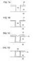
- FIG. 2illustrates the hydrolytic deposition of silanes.
- FIG. 3Aillustrates a reaction between surface-bound Si—OH groups and n-propyl trimethoxysilane (n-PTMS) in the presence of a Lewis base amine to form silane compounds.
- FIG. 3Billustrates the conversion of an alkoxy group into an Si—OH group.
- FIG. 3Cillustrates the formation of a horizontal network between adjacent silane compounds.
- FIGS. 4A-4Dillustrate the formation of a horizontal network between adjacent silane compounds in the presence of an organic acid.
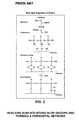
- FIG. 5Aillustrates a process chamber and chemical vapor delivery system for repairing and/or sealing semiconductor substrate with a nanoporous LKD material.
- FIG. 5Billustrates a chemical vapor delivery system for the vaporization and delivery of a liquid agent.
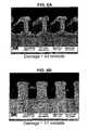
- FIGS. 6A-6Care scanning electron microscope (SEM) images characterizing the degree of repair along the sidewall of etched trenches for a vapor phase repaired sample, a supercritical CO 2 repaired sample and a sample with no repair.
- FIG. 7illustrates the ratio of carbon to silicon as a function of depth from a secondary ion mass spectrometry (SIMS) analysis for a vapor phase repaired sample, a supercritical CO 2 repaired sample, a sample with no repair and an as-deposited sample.
- SIMSsecondary ion mass spectrometry
- FIG. 1is an exemplary embodiment of a damascene manufacturing process.
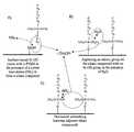
- FIG. 1Aillustrates a semiconductor substrate 100 with an overlying nanoporous LKD material layer 110 .
- openings 130are formed in nanoporous LKD material 110 .
- mask layer 120can be an organic photoresist and opening 130 can be formed by plasma etching.
- plasma etchingUpon the completion of plasma etching, mask layer 120 can be removed by ashing (i.e., dry etching in an oxygen-based plasma).
- barrier layer 140can be formed over the sidewall and bottom surfaces of opening 130 to protect the nanoporous LKD material 110 adjacent to the copper interconnects from being poisoned by copper atoms diffusing into the adjacent dielectric material.
- exemplary barrier materialsinclude titanium (Ti), titanium nitride (TiN), tantalum (Ta), tantalum nitride (TaN), ruthenium (Ru), ruthenium oxide (RuO x ) and alloys thereof.
- the barrier materialcan be coated by physical vapor deposition (PVD), atomic layer deposition (ALD), or the like.
- opening 130is filled with bulk copper layer 150 .
- bulk copper layer 150can be formed by depositing a seed layer, followed by electroless copper plating.
- the structureis planarized to remove the excess portion of bulk copper layer 150 by any suitable technique such as chemical mechanical planarization (CMP).
- CMPchemical mechanical planarization
- the damascene manufacturing processcan either be a single or double damascene process.
- either the via-first approach or the trench-first approachcan be used.
- openings 130e.g., vias or trenches
- the barrier material 140e.g., Ti, TiN, Ta, TaN, Ru or RuO x
- the barrier material 140can potential penetrate into interconnecting pores of nanoporous LKD material 110 , compromising the low dielectric value.
- structures formed from nanoporous LKD materialmay lack mechanical strength for subsequent processing steps (e.g., CMP). Thus, a need exists to repair damaged nanoporous LKD materials, sealing the surfaces of opening 130 , as well as enhancing the mechanical strength of LKD materials.
- At least a portion of carbon containing moietiescan be removed, resulting in nanoporous LKD materials having reduced hydrophobicity.
- carbon containing moietiesi.e., methyl or —CH 3 groups
- Si—C bondsare replaced with Si—OH (“silanol”) bonds or groups and the resulting dielectric layer loses its hydrophobicity as water molecules from the atmosphere or from subsequent wet cleaning steps form strong hydrogen-bonding interactions with the silanol groups.
- Si—C bondsSi—OH (“silanol”) bonds or groups
- si—OHSi—OH
- plasma damagecan extend to a depth of about 30 nm into the sidewalls of the openings.
- a depth of about 5 nm into the plasma damaged nanoporous LKD materialabout 25% of methyl groups (—CH 3 ) are lost (i.e., 25% of the Si—C bonds are replaced with Si—OH bonds or groups).
- Etch damaged nanoporous LKD materialscan be treated with alkoxysilane agents, which react with the Si—OH.
- alkoxysilane agentsone drawback of using alkoxysilane agents is that water is required to hydrolyze the alkoxy groups prior to condensation with the surface-bound Si—OH groups in a condensation step.
- one of the challenges associated with the use of compounds such as alkoxysilane agentsis the consistency of repair. This relates to the key role water plays in the chemical reaction between the alkoxysilane and the Si—OH groups. As illustrated in FIG. 2 , water is needed to hydrolyze the alkoxy groups prior to condensation with the Si—OH groups in a hydrolysis step.
- Lewis base aminese.g., ammonia, methyl amine, dimethyl amine or trimethyl amine
- the Lewis base aminesserve as a catalyst by forming a catalytic intermediary with the Si—OH groups.
- the catalytic intermediaryis formed because a hydrogen bond is developed between the Lewis base amine and the Si—OH group. The formation of this hydrogen bond drives the reaction forward, allowing the direct reaction of a Si—OH group with a alkoxy group of the alkoxysilane agent.
- the catalytic intermediaryis itself highly susceptible to reaction with the alkoxysilane agent.
- the reactionproduces the corresponding alcohol as a byproduct and the amine is freed to again hydrogen bond with additional Si—OH groups. Additionally, the alkoxysilane compounds can be horizontally networked to form three-dimensional horizontally networked structures, restoring the mechanical strength of the nanoporous LKD material.
- Organic acidscan also be used as catalysts by hydrolyzing alkoxysilanes to form Si—OH groups, which condense with surface-bound Si—OH groups in the presence of heat. Additionally, as illustrated in FIG. 4 , organic acids can be used to catalyze the reaction between water and substantially most of the residual alkoxy groups remaining on the repaired and/or horizontally networked nanoporous LKD material. In FIG. 4A , organic acids catalyze a hydrolytic reaction between water and the residual alkoxy groups, which produces Si—OH groups as shown in FIG. 4B . In FIG. 4C , Si—OH groups of adjacent silane compounds are then condensed to form the horizontal network.
- the organic acidcan be any organic acid having a pK a of up to about 7, more preferably up to about 4, and most preferably up to about 3.
- the organic acidscan include acetic acid, trifluoroacetic acid, trichloroacetic acid, citric acid, other fully halogenated or partially halogenated weak acids, and various combinations thereof.
- Alkoxysilane repair agentscan be characterized by smaller sized molecules, about 80 to about 125 atomic mass units (AMU) that can diffuse into the bulk of the nanoporous LKD materials via the interconnected porous network and react with silanol groups.
- AMUatomic mass units
- 50% or more of the lost methyl groupsare replenished with an alkyl group (e.g., ethyl, propyl, butyl groups), preferably about 75% to about 90% of the methyl groups are replenished.
- repair agentscan include methyl trimethoxysilane (CH 3 —Si—(O—CH 3 ) 3 ), dimethoxy dimethylsilane ((CH 3 ) 2 —Si—(OCH 3 ) 2 ), methoxy trimethylsilane ((CH 3 ) 3 —Si—OCH 3 ) or n-propyl trimethoxysilane (CH 3 —CH 2 —CH 2 —Si—(OCH 3 ) 3 or n-PTMS).
- CH 3 —Si—(O—CH 3 ) 3dimethoxy dimethylsilane
- methoxy trimethylsilane(CH 3 ) 3 —Si—OCH 3 ) or n-propyl trimethoxysilane (CH 3 —CH 2 —CH 2 —Si—(OCH 3 ) 3 or n-PTMS).
- Alkoxysilane sealing agentscan be characterized by larger sized molecules, from about 200 to about 400 AMU. Pore sealing of the nanoporous LKD material operates by the principal of size exclusion, in which the larger size of the alkoxysilane sealing agent has a reactive collision with a surface-bound Si—OH group, rather that passing through a pore opening of the nanoporous LKD material into a porous network. Alkoxysilane sealing agents react with surface silanol groups at a depth of less than about 3 to 4 nm, preferably at a depth of about 1 to 2 nm. Upon completion of the sealing process, the sidewall and bottom surfaces of the opening are covered with a film with a thickness of up to about 2 nm.
- This filmis effective to prevent the diffusion of overlying barrier materials into the interconnected pores of the nanoporous LKD material, however, it should be noted that vapor-phased catalysts can continue to diffuse into the nanoporous LKD material, due to their smaller molecular size.
- sealing agentscan include bis(dimethoxymethyl)siloxane, bis(methyldimethyloxysilylpropyl)-N-methylamine, bis(triethoxysilyl)ethane, 1,2-bis(trimethoxysilyl)hexane, bis(trimethoxysilylpropyl)amine or bis(3-triethoxysilyl)propyl)disulfide.
- Process chamber 200can be operational at pressures from about 1 mTorr to about 3750 Torr (i.e., about 5 bars) and at temperatures up to about 300° C.
- Nanoporous LKD material 110includes previously etched openings 130 (e.g., trenches or vias). Due to previous etching and/or removal of an overlying mask layer, the exposed surfaces of dielectric layer 110 are etch damaged. Although not illustrated in FIG. 5A , nanoporous LKD material 110 can overlie an intermediate layer such as a barrier layer and a conductive or semiconductive layer.
- nanoporous LKD materialcan include, but are not limited to, NANOGLASS® and HOSP® (manufactured by Honeywell International), carbon-doped oxides such as BLACK DIAMOND® (manufactured by APPLIED MATERIALS), CORAL® (manufactured by NOVELLUS), AURORA® (manufactured by ASM), ORION® (manufactured by Trikon), LKD-5109 (manufactured by JSR), and Nano-Clustered Silica or NCS (manufactured by FUJITSU).
- NANOGLASS® and HOSP®manufactured by Honeywell International
- carbon-doped oxidessuch as BLACK DIAMOND® (manufactured by APPLIED MATERIALS), CORAL® (manufactured by NOVELLUS), AURORA® (manufactured by ASM), ORION® (manufactured by Trikon), LKD-5109 (manufacture
- Substrate support 210can include an electrostatic chuck (ESC), mechanical clamp or other clamping mechanism and one or more heating elements for heating semiconductor substrate 100 to a temperature up to 300° C.
- ESCelectrostatic chuck
- Chemical vapor delivery systems 220 A, 220 B, 220 Ccan be used to sequentially deliver a catalyst, an alkoxysilane repair agent and an alkoxysilane sealing agent, respectively, to process chamber 200 .
- Vacuum pump 240can be used to evacuate gases from process chamber 200 once treatment with the catalyst, alkoxysilane repair agent or alkoxysilane sealing agent has been completed.
- the static gas pressureis maintained in process chamber 200 by backpressure regulator 250 , which functions to release the vapor into a chemical abatement system when the gas pressure exceeds a preselected pressure.
- FIG. 5Billustrates an embodiment of chemical vapor delivery system 220 for a liquid agent (e.g., catalyst, alkoxysilane repair agent or alkoxysilane sealing agent).
- a liquid agente.g., catalyst, alkoxysilane repair agent or alkoxysilane sealing agent.
- Liquid agent 222 from agent source 224can be placed in bubbler 226 , which is heated to an elevated temperature to vaporize the liquid agent 222 .
- An inert gase.g. nitrogen or argon
- gas source 228bubbles through the liquid agent 222 to deliver the vaporized agent to process chamber 200 through gas line 230 .
- Gas line 230can be heated to prevent the condensation of the vaporized agent within the gas line 230 .
- Semiconductor substrate 100is placed in contact with a vapor-phase catalyst prior to any repair and/or sealing process.
- the Lewis base amine or organic acid catalystfunctions to kinetically enhance the rate of condensation between alkoxysilanes and Si—OH groups without the primary hydrolysis step in the case of the Lewis base amine catalyst, and by accelerating hydrolysis in the case of the organic acid.
- the temperature of process chamber 200 and substrate support 210can be heated to a first temperature of about 60° C. to about 275° C., preferably about 100° C. to about 200° C.
- the temperature of the semiconductor substrate 100is preferably maintained at a temperature higher than the temperature of the vapor-phase agent throughout the entire process.
- the pressure of process chamber 200is maintained at a vacuum pressure to facilitate vaporization of the catalyst (e.g., about 0.5 Torr to about 10 Torr).
- Chemical vapor delivery system 220 Adelivers a vapor-phase catalyst to the process chamber 200 to treat semiconductor substrate 100 .
- Semiconductor substrate 100is placed in contact with the vapor-phase catalyst in an amount effective to interact with silanol groups in the etch damaged region.
- the vapor-phase catalystcan form a sub-monolayer or monolayer of the catalyst on the exterior surfaces of opening 130 (i.e., sidewall surfaces) and on interior surfaces of the interconnected pores in the nanoporous LKD material 110 .
- a plasma damaged regioncan extend to depth to about 30 nm into the sidewalls of the openings 130 .
- the catalystis delivered to the process chamber 200 to increase static pressure of the vapor-phase catalyst in process chamber 200 to about 20 Torr to about 1500 Torr (i.e., about 2 bars), preferably about 100 Torr to about 760 Torr.
- the volume of process chamber 200is about 1.1 liters.
- the contact time of the vapor-phase catalystcan be about 10 seconds to about 60 seconds, preferably about 20 to about 30 seconds.
- the remaining vapor-phase catalystis removed from the process chamber 200 either by dynamic flow of an inert gas or by vacuum pump 240 , until a pressure of below about 5 Torr is achieved.
- a dynamic vacuumcan be maintained by flowing the vapor-phase catalyst into processing chamber during the simultaneous operation of vacuum pump 240 and/or a back pressure regulator 250 .
- Exemplary Lewis base aminescan include ammonia (NH 3 ), methyl amine (CH 3 NH 2 ), dimethyl amine ((CH 3 ) 2 NH) or trimethyl amine (N(CH 3 ) 3 ), or corresponding primary, secondary, or tertiary ethyl substituted amines.
- Exemplary organic acidscan include acetic acid, trifluoroacetic acid, trichloroacetic acid, citric acid, other fully halogenated or partially halogenated weak acids.
- the organic acidcan be mixed with water to form an aqueous solution, which is vaporized.
- the temperature of the process chamber 200 and substrate support 210 and static pressureis selected to prevent condensation of the Lewis base amine catalyst or organic acid.
- an organic acid catalystis used, to maximize alkoxysilane reactions with surface-bound Si—OH groups, excess vapor phase organic acid is preferably evacuated before the introduction of alkoxysilane repair and/or sealing agents, to prevent reactions between the organic acid and alkoxysilane in the vapor phase.
- the pressure of the process chamber 200is decreased to a vacuum pressure to facilitate vaporization of the alkoxysilane repair agent (e.g., about 0.5 Torr to about 10 Torr).
- Process chamber 200can be optionally backfilled with an inert gas (e.g., nitrogen or argon) before evacuating to a vacuum pressure.
- the temperature of process chamber 200 and substrate support 210is maintained at the first temperature of about 60° C. to about 275° C., preferably about 100° C. to about 200° C.
- Chemical vapor delivery system 220 Bdelivers the alkoxysilane repair agent to the process chamber 200 to treat semiconductor substrate 100 .
- Semiconductor substrate 100is placed in contact with the alkoxysilane repair agent in an amount effective to restore at least 50% of the lost methyl groups with an alkyl group (e.g., ethyl, propyl, butyl groups), preferably about 75% to about 90% of the lost methyl groups.
- an alkyl groupe.g., ethyl, propyl, butyl groups
- a fixed amount of alkoxysilane repair agentis delivered such that the static pressure of repair agent in process chamber 200 is about 20 Torr to about 1500 Torr (i.e., about 2 bars), preferably about 100 Torr to about 760 Torr.
- the total contact time of semiconductor substrate 100 with the vapor-phase alkoxysilane repair agent at the first temperaturecan be about 10 seconds to about 180 seconds, preferably about 20 seconds to about 60 seconds.
- a dynamic vacuumcan be maintained by flowing the vapor-phase repair agent into processing chamber 200 during the simultaneous operation of vacuum pump 240 and/or a back-pressure regulator 250 .
- the nanoporous LKD material 110is preferably placed in contact with the alkoxysilane repair agent at a second temperature.
- the temperature of the wafer support 210can be increased from the first temperature to a second temperature of about 80° C. to about 300° C., preferably about 150° C. to about 250° C.
- the total contact time of semiconductor substrate 100 with the vapor-phase alkoxysilane repair agent at the second temperaturecan be about 10 seconds to about 180 seconds, preferably about 20 seconds to about 60 seconds.
- Exemplary alkoxysilane repair agentscan include methyl trimethoxysilane (CH 3 —Si—(O—CH 3 ) 3 ), dimethoxy dimethylsilane ((CH 3 ) 2 —Si—(OCH 3 ) 2 ), methoxy trimethylsilane ((CH 3 ) 3 —Si—OCH 3 ) or n-propyl trimethoxysilane (CH 3 —CH 2 —CH 2 —Si—(OCH 3 ) 3 or n-PTMS).
- the temperature of the process chamber 200 and substrate support 210 and static pressureis selected to prevent condensation of the alkoxysilane repair agent.
- Condensation of the alkoxysilane repair agent on the surface of the LKD materialcan be detrimental, preventing the uniform penetration of the alkoxysilane repair agent into the nanoporous LKD material.
- the nanoporous LKD materialis placed in contact with an agent below its saturation point (i.e., vapor pressure at a given temperature is less than 760 Torr). Under these conditions, no saturation (i.e., formation of liquid agent) can occur on the nanoporous LKD material.
- the pressure of vacuum chamberis decreased to about 0.5 Torr for about 30 seconds to about 180 seconds.
- the pressure in the chambercan be maintained at a static level and a dynamic flow of an inert flush gas can be used to remove the residual agent.
- the above described process steps for contacting the vapor-phase catalyst and vapor-phase alkoxysilane repair agent with the nanoporous LKD materialcan be repeated one or more times on the same semiconductor substrate 100 at the second temperature to increase the reactivity of the alkoxysilane repair agent.
- contacting the vapor-phase catalyst and the alkoxysilane repair agent with the nanoporous LKD materialcan be repeated up to ten times.
- the surface of the LKD material 110can be sealed by contacting semiconductor substrate 100 with an alkoxysilane sealing agent. As described above, this sealing step covers the sidewall and bottom surfaces of the openings with an alkoxysilane film with a thickness of up to about 2 nm, effective to prevent the diffusion of an overlying barrier material into the interconnected pores of the nanoporous LKD material.
- the LKD material 110can be optionally placed in contact with the vapor-phase catalyst prior to the sealing process.
- alkoxysilane sealing agentscan include bis(dimethoxymethyl)siloxane, bis(methyldimethoxysilylpropyl)-N-methylamine, bis(triethoxysilyl)ethane, 1,2-bis(trimethoxysilyl) hexane, bis(trimethoxysilylpropyl)amine or bis(3-(triethoxysilyl)propyl)disulfide.
- the surface of the LKD material 110can be sealed by contacting the surface with an alkoxysilane sealing agent without an initial repair step, if plasma damage to the sidewalls and bottom of opening 130 is minimal and repair is not desired. In this instance, the semiconductor substrate 100 and LKD material 110 would be placed in contact with the vapor-phase catalyst prior to the sealing process.
- the alkoxysilane compoundscan be horizontally networked to form three-dimensional horizontally networked structures, restoring the mechanical strength of the nanoporous LKD material.
- This horizontal networking stepcan be preformed by treating the LKD material with the organic acid (e.g., acetic acid, trifluoroacetic acid, trichloroacetic acid, citric acid) described above to catalyze a hydrolytic reaction between water and the residual alkoxy groups, as illustrated in FIG. 4 .
- the organic acid vaporcan be delivered to process chamber 200 using the chemical vapor delivery system 220 with the temperature range, pressure range and time range described above.
- the LKD materialis placed in contact with a vapor phase catalyst in an amount effective to horizontally network the alkoxysilane repair and/or sealing agents.
- the temperature of the semiconductor substrate 100is increased to about 200° C. to about 300° C. for about 60 seconds to about 360 seconds.
- This heating stepfacilitates condensation reaction between adjacent alkoxysilane molecules to form three-dimensional horizontally networked structures, restoring the mechanical strength of the nanoporous LKD material.
- This heating stepcan either occur inside process chamber 200 or semiconductor substrate 100 can be removed and heated on a hot plate.
- semiconductor substrate 100can be subjected to subsequent damascene processing steps, including the deposition of barrier layer 140 in opening 130 , formation of bulk metal layer 150 in opening 130 and planarization of the entire structure, as illustrated in FIGS. 1B-1D .
- the vapor-phase sealing of the sidewall and bottom surfaces of opening 130 in nanoporous LKD material 110prevents the materials used in forming barrier layer 140 (e.g., Ti, TiN, Ta, TaN, Ru or RuO x ) from penetrating into the interconnected pores of nanoporous LKD material 110 .
- Vapor-phase repair and sealing of nanoporous LKD material layer 110creates a more robust structure that can withstand further mechanical processing steps, including CMP.
- semiconductor substrate 100 with an etch damaged nanoporous LKD material 110is repaired using vapor-phase methyl trimethoxysilane (CH 3 —Si—(O—CH 3 ) 3 ) as a repair agent and vapor-phase diethyl amine ((CH 3 ) 2 NH) as a catalyst.
- vapor-phase methyl trimethoxysilaneCH 3 —Si—(O—CH 3 ) 3
- vapor-phase diethyl amine(CH 3 ) 2 NH)
- Semiconductor substrate 100 with an etch damaged low-k dielectric layer 110is placed on substrate support 210 of process chamber 200 .
- the process chamber 200is evacuated to a pressure below 50 Torr and the substrate support 210 and process chamber 200 are heated to a first temperature of about 100° C.
- Diethyl amine vaporis delivered to process chamber 200 to a static pressure of 700 Torr from chemical vapor delivery system 220 A.
- the semiconductor substrate 100is placed in contact with the diethyl amine vapor for about 20 seconds.
- the vaporis evacuated with vacuum pump 240 under a dynamic vacuum to reduce the pressure of the process chamber 200 to about 5 Torr or less, to remove residual amine and to facilitate vaporization of the methyl trimethoxysilane, which is a liquid under ambient conditions.
- Methyl trimethoxysilane vapor(CH 3 —Si—(O—CH 3 ) 3 ) is flowed into process chamber 200 from chemical vapor delivery system 220 B until a static pressure of 400 Torr is achieved.
- Semiconductor substrate 100is placed in contact with the vapor-phase methyl trimethoxysilane for about 20 seconds at the first temperature of about 100° C.
- the temperature of substrate support 210is increased from the first temperature of about 100° C. to a second temperature of about 150° C. and the semiconductor substrate 100 is placed in contact with the vapor-phase methyl trimethoxysilane for an additional 30 seconds.
- the vaporis evacuated with vacuum pump 240 under a dynamic vacuum to reduce the pressure of the process chamber 200 to about 0.5 Torr or less for about 60 seconds, to remove excess methyl trimethoxysilane vapor and reaction by-products.
- semiconductor substrate 100 with an etch damaged nanoporous LKD material 110is sealed using vapor-phase bis(3-methyldimethoxysilyl-propyl)-N-methylamine as a sealing agent with vapor-phase methyl amine (CH 3 NH 2 ) as a catalyst.
- Semiconductor substrate 100 with an etch damaged low-k dielectric layer 110is placed on substrate support 210 of process chamber 200 .
- the process chamber 200is evacuated to a pressure below 50 Torr and substrate support 210 and process chamber 200 are heated to a first temperature of about 150° C.
- Methyl amine vaporis delivered into process chamber 200 to a static pressure of 1800 Torr from chemical vapor delivery system 220 A.
- the semiconductor substrate 100is placed in contact with the methyl amine vapor for about 60 seconds.
- the vaporis evacuated with vacuum pump 240 under a dynamic vacuum to reduce the pressure of the process chamber 200 to about 300 Torr or less.
- Flowing bis(3-methyldimethoxysilyl-propyl)-N-methylamineis introduced into process chamber 200 from chemical vapor delivery system 220 C with dry nitrogen as a carrier gas at approximately 3000 sccm.
- the pressureis maintained to 400 Torr by the simultaneous operation of vacuum pump 240 .
- Semiconductor substrate 100is placed in contact with flowing bis(3-methyldimethoxysilyl-propyl)-N-methylamine for about 180 seconds at about 150° C.
- the vaporis evacuated with vacuum pump 240 under a dynamic vacuum to reduce the pressure of the process chamber 200 to about 2 Torr or less for about 60 seconds.
- Silicon substrate samples with an overlying nanoporous LKD material(JSR LKD-5109, manufactured by JSR Corporation) were prepared.
- the sampleswere coated with photoresist, patterned and subjected to reactive ion etching (RIE) to form trenches, followed by oxygen ashing to remove the photoresist.
- RIEreactive ion etching
- the RIE and photoresist removalresult in a plasma damaged region surrounding the etched openings in the patterned areas.
- a first sample with a plasma damaged JSR LKD-5109 layerwas placed in contact with a vapor phase trifluoroacetic acid catalyst prior to contact with a vapor-phase n-propyl trimethoxysilane (n-PTMS) repair agent.
- a second sample with a plasma damaged JSR LKD-5109 layerwas treated with an n-PTMS repair agent and a trifluoroacetic acid catalyst dissolved in supercritical CO 2 (SCCO 2 ).
- a third samplewas a control sample with an unrepaired plasma damaged JSR LKD-5109 layer.
- a fourth sampleis another control sample with an as-deposited JSR LKD-5109 layer (i.e., not subjected to plasma etching).
- Sampleswere analyzed by scanning electron microscopy (SEM) to characterize the degree of repair along the sidewalls of the etched trenches and secondary ion mass spectrometry (SIMS) to characterize the ratio of carbon to silicon over the surface of the JSR LKD-5109 layer to a depth of about 150 nm.
- SEMscanning electron microscopy
- SIMSsecondary ion mass spectrometry
- the first sample containing the plasma etch damaged JSR LKD-5109was placed on substrate support 210 of process chamber 200 .
- the process chamber 200was evacuated to a pressure below 50 Torr and the substrate support 210 and process chamber 200 are heated to a first temperature of about 135° C.
- a 3:1 mixture of trifluoroacetic acid to waterwas vaporized and introduced into process chamber 200 to a pressure of 900 Torr from chemical vapor delivery system 220 A.
- the first samplewas placed in contact with the trifluoroacetic acid vapor for about 120 seconds before process chamber 200 was backfilled with nitrogen and evacuated.
- Vapor-phase n-PTMS repair agentwas delivered into process chamber 200 by chemical vapor delivery system 220 B to treat the second sample for about 5 minutes at a static pressure of about 1000 Torr.
- the process chamber 200was backfilled with nitrogen gas and the first sample was maintained at a temperature of 135° C. for about 2 minutes.
- the first samplewas then removed from the process chamber and heated on a hotplate from about 120 seconds at about 250° C.
- the second samplewas placed in a heated pressure vessel (i.e., about 140° C.) which was subsequently sealed and pressurized to about 97,500 Torr (about 130 bar) with supercritical carbon dioxide (SCCO 2 ).
- SCCO 2supercritical carbon dioxide
- a 3:1 mixture of trifluoroacetic acid to waterwas added using a high-pressure injection loop by pumping additional SCCO 2 into the vessel and flushing catalyst into the vessel.
- the concentration of the catalyst after completion of additionwas approximately 1% by volume and the resulting pressure was about 150,000 Torr (about 200 bar) at about 140° C.
- the SCCO 2 solution containing acid catalystwas flushed from the chamber by addition of pure SCCO 2 .
- the flushingresulted in approximately 6 fluid turnovers (i.e., the amount of flow for a period of time required to equal the volume of the vessel) over a period of about 2 minutes.
- the pressure in the vesselwas reduced to about 97,500 Torr (about 130 bar) at about 140° C. by removal of SCCO 2 .
- An n-propyl trimethoxysilane (n-PTMS) repair agentwas then added to the vessel using a high-pressure injection loop by pumping additional SCCO 2 into the vessel.
- the concentration of the repair agentwas approximately 2% by volume and the final pressure in the vessel was about 150,000 Torr (about 200 bar) at 140° C.
- the vesselwas flushed with pure SCCO 2 for a period and at a flow rate to allow for 8 fluid turnovers over a period of about 2 minutes.
- the pressure in the vesselwas reduced to ambient and the second sample was removed.
- the first samplei.e., n-PTMS vapor-phase repaired
- second samplei.e., n-PTMS SCCO 2 repaired
- third samplei.e., no repair
- SEMSEM image of the first sample (i.e., n-PTMS vapor phase repaired) in which undercutting was measured at a depth of about 11 nm into the sidewall of the trench.
- FIG. 6Billustrates an SEM image of the second sample (i.e., n-PTMS SCCO 2 repaired) in which undercutting was measured at a depth of about 11 nm into the sidewall of the trench.
- FIG. 6Cillustrates an SEM image of the third sample (i.e., no repair), in which undercutting was measured at a depth of about 43 nm into the sidewall of the trench.
- FIGS. 6B-6Cillustrate that the vapor phase repair is as effective as SCCO 2 in repairing etch damaged nanoporous LKD materials.
- the first samplei.e., n-PTMS vapor-phase repaired
- second samplei.e., n-PTMS SCCO 2 repaired
- third samplei.e., no repair
- fourth samplei.e., as deposited JSR LKD-5109
- the carbon to silicon ratiodecreased to about 0.45 to about 0.55.
- the carbon to silicon ratioincreased to about 0.6 to about 0.8, above the carbon to silicon ratio of the as-deposited JSR LKD-5109. This is because the repair process replaces lost methyl groups (—CH 3 ) with propyl groups (—C 3 H 7 ), thus increasing the carbon to silicon ratio in the damaged regions.
- the first sample (filled circles in FIG. 7 )there is a significant increase in the carbon to silicon ratio of up to about 1.45. This is a possible indication that the vapor-phase repair more effectively densifies n-PTMS and/or sealing of the porous surface.
Landscapes
- Engineering & Computer Science (AREA)
- Physics & Mathematics (AREA)
- Condensed Matter Physics & Semiconductors (AREA)
- General Physics & Mathematics (AREA)
- Manufacturing & Machinery (AREA)
- Computer Hardware Design (AREA)
- Microelectronics & Electronic Packaging (AREA)
- Power Engineering (AREA)
- Plasma & Fusion (AREA)
- Internal Circuitry In Semiconductor Integrated Circuit Devices (AREA)
- Formation Of Insulating Films (AREA)
- Drying Of Semiconductors (AREA)
Abstract
Description
This application is a national stage application under 35 USC §371 of International Application Number PCT/US2008/013471, filed Dec. 8, 2008, the international Application being published in English. This application also claims priority under 35 USC §119 to U.S. Provisional Application No. 61/008,148, filed Dec. 19, 2007, the entire content of which is hereby incorporated by reference.
As the dimensions of integrated circuit devices continue to decrease, the time delay for the propagation of a signal between multiple transistors (i.e., propagation delay) has become an increasingly important parameter in determining device performance. Propagation delay is proportional to the product of the resistance of a metal interconnect line (R) and the capacitance of the interlevel dielectric insulation material (C) (also referred to as RC delay). Thus, to minimize propagation delay, it is beneficial to incorporate an insulating material with a low dielectric constant material in combination with a high conductivity metal (or low resistivity metal). Low-k dielectric (LKD) materials (k<3.0), such as organosilicate glass (OSG), organosilicate glass (OSG), tetraethylorthosilicate (TEOS), fluorinated silica glass (FSG) and carbon-doped oxides, are also gaining interest as alternatives to silicon oxide (k=3.8-4.0). To obtain lower dielectric values, the LKD material can contain an interconnected nanoporous structure, which entraps air (k=1) to lower the overall k value of the bulk LKD. Likewise, copper (Cu) has gained considerable interest as a metal for interconnect lines, as an alternative to the more conventional aluminum (Al) interconnect metal (R=3.0-5.0 μΩ-cm), because of its lower resistivity value (R<2 μΩ-cm).
Because copper does not readily form volatile by-products, conventional or subtractive etching techniques are inadequate. Thus, damascene manufacturing processes are necessary to form patterned copper interconnect lines, processes that involve depositing conductive material in previously patterned openings (e.g., trenches or vias). Thus, damascene processing necessitates the etching of previously patterned openings in the LKD material. This is performed by patterning openings in a mask layer, such as photoresist, on a dielectric layer in the shape of a trench or via, followed by wet or dry etching. However, the etching, ashing or cleaning of LKD materials can potentially damage the LKD material.
A method of treating a nanoporous low-k dielectric material formed on a semiconductor substrate is provided. The low-k dielectric material has etched openings with an etch damaged region containing silanol groups on exterior surfaces of the etched openings and on interior surfaces of interconnected pores. First, the low-k dielectric material is contacted with a vapor phase catalyst in an amount effective to form hydrogen bonds between the catalyst and the silanol groups in the etch damaged region, forming a catalytic intermediary. Second, the low-k dielectric material is contacted with a vapor phase alkoxysilane repair agent in an amount effective to react with about 50% or more of the silanol groups in the etch damaged region, such that the alkoxysilane repair agent reacts with the catalytic intermediary; and/or the low-k dielectric material is contacted with a vapor phase alkoxysilane sealing agent in an amount effective to prevent diffusion of an overlying barrier layer into the interconnected pores, such that the alkoxysilane sealing agent reacts with the catalytic intermediary.
In another embodiment, a method of treating a nanoporous low-k dielectric material formed on a semiconductor substrate is provided. The low-k dielectric material has etched openings with an etch damaged region containing silanol groups on exterior surfaces of the etched openings and on interior surfaces of interconnected pores. First, the low-k dielectric material is contacted with a vapor phase organic acid catalyst in an amount effective to form hydrogen bonds between the catalyst and the silanol groups in the etch damaged region, forming a catalytic intermediary. Second, the low-k dielectric material is contacted with a vapor phase alkoxysilane repair agent in an amount effective to react with about 50% or more of the silanol groups in the etch damaged region, such that the alkoxysilane repair agent reacts with the catalytic intermediary; and/or the low-k dielectric material is contacted with a vapor phase alkoxysilane sealing agent in an amount effective to prevent diffusion of an overlying barrier layer into the interconnected pores, such that the alkoxysilane sealing agent reacts with the catalytic intermediary.
InFIG. 1B ,barrier layer 140 can be formed over the sidewall and bottom surfaces of opening130 to protect thenanoporous LKD material 110 adjacent to the copper interconnects from being poisoned by copper atoms diffusing into the adjacent dielectric material. Exemplary barrier materials include titanium (Ti), titanium nitride (TiN), tantalum (Ta), tantalum nitride (TaN), ruthenium (Ru), ruthenium oxide (RuOx) and alloys thereof. For example, the barrier material can be coated by physical vapor deposition (PVD), atomic layer deposition (ALD), or the like.
InFIG. 1C , opening130 is filled withbulk copper layer 150. For example,bulk copper layer 150 can be formed by depositing a seed layer, followed by electroless copper plating. As illustrated inFIG. 1D , the structure is planarized to remove the excess portion ofbulk copper layer 150 by any suitable technique such as chemical mechanical planarization (CMP).
The damascene manufacturing process can either be a single or double damascene process. For the latter process, either the via-first approach or the trench-first approach can be used.
Prior to the successful implementation of nanoporous LKD material in a damascene structure, several obstacles must be overcome. First, the process of forming openings130 (e.g., vias or trenches) by etching and removal ofmask layer 120 by ashing can potentially damage the nanoporous LKD material. Second, the barrier material140 (e.g., Ti, TiN, Ta, TaN, Ru or RuOx) can potential penetrate into interconnecting pores ofnanoporous LKD material 110, compromising the low dielectric value. Third, due to the presence of interconnecting pores in many nanoporous LKD materials, structures formed from nanoporous LKD material may lack mechanical strength for subsequent processing steps (e.g., CMP). Thus, a need exists to repair damaged nanoporous LKD materials, sealing the surfaces of opening130, as well as enhancing the mechanical strength of LKD materials.
During plasma etching and ashing, at least a portion of carbon containing moieties (i.e., methyl or —CH3groups) can be removed, resulting in nanoporous LKD materials having reduced hydrophobicity. When the carbon containing moieties are removed from the nanoporous LKD materials, Si—C bonds are replaced with Si—OH (“silanol”) bonds or groups and the resulting dielectric layer loses its hydrophobicity as water molecules from the atmosphere or from subsequent wet cleaning steps form strong hydrogen-bonding interactions with the silanol groups. The presence of water, which has a k-value of about 70, results in a significant increase in the k-value of the nanoporous LKD material. For example, during the plasma etching of openings (e.g., vias or trenches) in the nanoporous LKD material, plasma damage can extend to a depth of about 30 nm into the sidewalls of the openings. At a depth of about 5 nm into the plasma damaged nanoporous LKD material, about 25% of methyl groups (—CH3) are lost (i.e., 25% of the Si—C bonds are replaced with Si—OH bonds or groups).
Etch damaged nanoporous LKD materials can be treated with alkoxysilane agents, which react with the Si—OH. However, one drawback of using alkoxysilane agents is that water is required to hydrolyze the alkoxy groups prior to condensation with the surface-bound Si—OH groups in a condensation step. Thus, one of the challenges associated with the use of compounds such as alkoxysilane agents is the consistency of repair. This relates to the key role water plays in the chemical reaction between the alkoxysilane and the Si—OH groups. As illustrated inFIG. 2 , water is needed to hydrolyze the alkoxy groups prior to condensation with the Si—OH groups in a hydrolysis step.
Differing levels of hydrogen-bonded water on surfaces, driven by atmospheric moisture, directly affect reaction efficiency. Without the use of catalysts, the chemical reaction between the alkoxysilanes and the Si—OH groups mandates the presence of some water. Further, if a consistent result is desired, substantially the same level of hydration has to be maintained from sample to sample.
Lewis base amines (e.g., ammonia, methyl amine, dimethyl amine or trimethyl amine) can be used as catalysts to enhance the rate of condensation between alkoxysilanes and Si—OH groups without the hydrolysis step. As illustrated inFIG. 3 , the Lewis base amines serve as a catalyst by forming a catalytic intermediary with the Si—OH groups. The catalytic intermediary is formed because a hydrogen bond is developed between the Lewis base amine and the Si—OH group. The formation of this hydrogen bond drives the reaction forward, allowing the direct reaction of a Si—OH group with a alkoxy group of the alkoxysilane agent. The catalytic intermediary is itself highly susceptible to reaction with the alkoxysilane agent. The reaction produces the corresponding alcohol as a byproduct and the amine is freed to again hydrogen bond with additional Si—OH groups. Additionally, the alkoxysilane compounds can be horizontally networked to form three-dimensional horizontally networked structures, restoring the mechanical strength of the nanoporous LKD material.
Organic acids can also be used as catalysts by hydrolyzing alkoxysilanes to form Si—OH groups, which condense with surface-bound Si—OH groups in the presence of heat. Additionally, as illustrated inFIG. 4 , organic acids can be used to catalyze the reaction between water and substantially most of the residual alkoxy groups remaining on the repaired and/or horizontally networked nanoporous LKD material. InFIG. 4A , organic acids catalyze a hydrolytic reaction between water and the residual alkoxy groups, which produces Si—OH groups as shown inFIG. 4B . InFIG. 4C , Si—OH groups of adjacent silane compounds are then condensed to form the horizontal network. The organic acid can be any organic acid having a pKaof up to about 7, more preferably up to about 4, and most preferably up to about 3. The organic acids can include acetic acid, trifluoroacetic acid, trichloroacetic acid, citric acid, other fully halogenated or partially halogenated weak acids, and various combinations thereof.
Such Lewis base amine and organic acid catalysts have been demonstrated to kinetically enhance the rate of condensation between alkoxysilanes and surface-bound Si—OH groups without the primary hydrolysis step in a supercritical CO2(or SCCO2) medium, as disclosed in commonly-assigned U.S. patent application Ser. No. 11/475,206, which is incorporated by reference in its entirety.
Described herein is a novel method of repairing and/or sealing etch damaged nanoporous LKD material using vapor-phase mono-, di- or tri-functional alkoxysilane agents coupled with vapor-phase Lewis base amine or organic acid catalysts. Repair agents and sealing agents can be generically represented as Si—(R)x(OR′)y, where y≧1, x+y=4, R is an alkyl, aryl or hydroxyl group and R′ is an alkyl or aryl group, preferably methyl or ethyl.
Alkoxysilane repair agents can be characterized by smaller sized molecules, about 80 to about 125 atomic mass units (AMU) that can diffuse into the bulk of the nanoporous LKD materials via the interconnected porous network and react with silanol groups. Upon the completion of repair, 50% or more of the lost methyl groups are replenished with an alkyl group (e.g., ethyl, propyl, butyl groups), preferably about 75% to about 90% of the methyl groups are replenished.
Examples of repair agents can include methyl trimethoxysilane (CH3—Si—(O—CH3)3), dimethoxy dimethylsilane ((CH3)2—Si—(OCH3)2), methoxy trimethylsilane ((CH3)3—Si—OCH3) or n-propyl trimethoxysilane (CH3—CH2—CH2—Si—(OCH3)3or n-PTMS).
Alkoxysilane sealing agents can be characterized by larger sized molecules, from about 200 to about 400 AMU. Pore sealing of the nanoporous LKD material operates by the principal of size exclusion, in which the larger size of the alkoxysilane sealing agent has a reactive collision with a surface-bound Si—OH group, rather that passing through a pore opening of the nanoporous LKD material into a porous network. Alkoxysilane sealing agents react with surface silanol groups at a depth of less than about 3 to 4 nm, preferably at a depth of about 1 to 2 nm. Upon completion of the sealing process, the sidewall and bottom surfaces of the opening are covered with a film with a thickness of up to about 2 nm. This film is effective to prevent the diffusion of overlying barrier materials into the interconnected pores of the nanoporous LKD material, however, it should be noted that vapor-phased catalysts can continue to diffuse into the nanoporous LKD material, due to their smaller molecular size.
Examples of sealing agents can include bis(dimethoxymethyl)siloxane, bis(methyldimethyloxysilylpropyl)-N-methylamine, bis(triethoxysilyl)ethane, 1,2-bis(trimethoxysilyl)hexane, bis(trimethoxysilylpropyl)amine or bis(3-triethoxysilyl)propyl)disulfide.
As illustrated inFIG. 5A ,semiconductor substrate 100 with ananoporous LKD material 110 is placed inprocess chamber 200 for the treatment of damage resulting from etching and/or photoresist ashing.Process chamber 200 can be operational at pressures from about 1 mTorr to about 3750 Torr (i.e., about 5 bars) and at temperatures up to about 300° C.
Examples of nanoporous LKD material can include, but are not limited to, NANOGLASS® and HOSP® (manufactured by Honeywell International), carbon-doped oxides such as BLACK DIAMOND® (manufactured by APPLIED MATERIALS), CORAL® (manufactured by NOVELLUS), AURORA® (manufactured by ASM), ORION® (manufactured by Trikon), LKD-5109 (manufactured by JSR), and Nano-Clustered Silica or NCS (manufactured by FUJITSU). One characteristic of many nanoporous LKD materials is the presence of an interconnected pore structure, which has a narrow pore size distribution with an average pore size of about 2 nanometers.
Chemicalvapor delivery systems chamber 200.Vacuum pump 240 can be used to evacuate gases fromprocess chamber 200 once treatment with the catalyst, alkoxysilane repair agent or alkoxysilane sealing agent has been completed. The static gas pressure is maintained inprocess chamber 200 bybackpressure regulator 250, which functions to release the vapor into a chemical abatement system when the gas pressure exceeds a preselected pressure.
Initially, the pressure ofprocess chamber 200 is maintained at a vacuum pressure to facilitate vaporization of the catalyst (e.g., about 0.5 Torr to about 10 Torr). Chemicalvapor delivery system 220A delivers a vapor-phase catalyst to theprocess chamber 200 to treatsemiconductor substrate 100.Semiconductor substrate 100 is placed in contact with the vapor-phase catalyst in an amount effective to interact with silanol groups in the etch damaged region. For example, the vapor-phase catalyst can form a sub-monolayer or monolayer of the catalyst on the exterior surfaces of opening130 (i.e., sidewall surfaces) and on interior surfaces of the interconnected pores in thenanoporous LKD material 110. In one embodiment, a plasma damaged region can extend to depth to about 30 nm into the sidewalls of theopenings 130.
In one embodiment, the catalyst is delivered to theprocess chamber 200 to increase static pressure of the vapor-phase catalyst inprocess chamber 200 to about 20 Torr to about 1500 Torr (i.e., about 2 bars), preferably about 100 Torr to about 760 Torr. The volume ofprocess chamber 200 is about 1.1 liters. The contact time of the vapor-phase catalyst can be about 10 seconds to about 60 seconds, preferably about 20 to about 30 seconds. After treatment with the vapor-phase catalyst has been completed, the remaining vapor-phase catalyst is removed from theprocess chamber 200 either by dynamic flow of an inert gas or byvacuum pump 240, until a pressure of below about 5 Torr is achieved. In another embodiment, a dynamic vacuum can be maintained by flowing the vapor-phase catalyst into processing chamber during the simultaneous operation ofvacuum pump 240 and/or aback pressure regulator 250.
Exemplary Lewis base amines can include ammonia (NH3), methyl amine (CH3NH2), dimethyl amine ((CH3)2NH) or trimethyl amine (N(CH3)3), or corresponding primary, secondary, or tertiary ethyl substituted amines. Exemplary organic acids can include acetic acid, trifluoroacetic acid, trichloroacetic acid, citric acid, other fully halogenated or partially halogenated weak acids. In one embodiment, the organic acid can be mixed with water to form an aqueous solution, which is vaporized. Depending upon the specific Lewis base amine or organic acid, the temperature of theprocess chamber 200 andsubstrate support 210 and static pressure is selected to prevent condensation of the Lewis base amine catalyst or organic acid. If an organic acid catalyst is used, to maximize alkoxysilane reactions with surface-bound Si—OH groups, excess vapor phase organic acid is preferably evacuated before the introduction of alkoxysilane repair and/or sealing agents, to prevent reactions between the organic acid and alkoxysilane in the vapor phase.
After treatment with the vapor-phase catalyst has been completed, the pressure of theprocess chamber 200 is decreased to a vacuum pressure to facilitate vaporization of the alkoxysilane repair agent (e.g., about 0.5 Torr to about 10 Torr).Process chamber 200 can be optionally backfilled with an inert gas (e.g., nitrogen or argon) before evacuating to a vacuum pressure. The temperature ofprocess chamber 200 andsubstrate support 210 is maintained at the first temperature of about 60° C. to about 275° C., preferably about 100° C. to about 200° C. Chemicalvapor delivery system 220B delivers the alkoxysilane repair agent to theprocess chamber 200 to treatsemiconductor substrate 100.Semiconductor substrate 100 is placed in contact with the alkoxysilane repair agent in an amount effective to restore at least 50% of the lost methyl groups with an alkyl group (e.g., ethyl, propyl, butyl groups), preferably about 75% to about 90% of the lost methyl groups.
In one embodiment, a fixed amount of alkoxysilane repair agent is delivered such that the static pressure of repair agent inprocess chamber 200 is about 20 Torr to about 1500 Torr (i.e., about 2 bars), preferably about 100 Torr to about 760 Torr. The total contact time ofsemiconductor substrate 100 with the vapor-phase alkoxysilane repair agent at the first temperature can be about 10 seconds to about 180 seconds, preferably about 20 seconds to about 60 seconds. In another embodiment, a dynamic vacuum can be maintained by flowing the vapor-phase repair agent intoprocessing chamber 200 during the simultaneous operation ofvacuum pump 240 and/or a back-pressure regulator 250.
To increase the reactivity of the alkoxysilane repair agent with the silanol groups in the bulk of thenanoporous LKD material 110, after contact with the alkoxysilane repair agent at a first temperature has been completed, thenanoporous LKD material 110 is preferably placed in contact with the alkoxysilane repair agent at a second temperature. The temperature of thewafer support 210 can be increased from the first temperature to a second temperature of about 80° C. to about 300° C., preferably about 150° C. to about 250° C. The total contact time ofsemiconductor substrate 100 with the vapor-phase alkoxysilane repair agent at the second temperature can be about 10 seconds to about 180 seconds, preferably about 20 seconds to about 60 seconds.
Exemplary alkoxysilane repair agents can include methyl trimethoxysilane (CH3—Si—(O—CH3)3), dimethoxy dimethylsilane ((CH3)2—Si—(OCH3)2), methoxy trimethylsilane ((CH3)3—Si—OCH3) or n-propyl trimethoxysilane (CH3—CH2—CH2—Si—(OCH3)3or n-PTMS). Depending upon the specific alkoxysilane repair agent, the temperature of theprocess chamber 200 andsubstrate support 210 and static pressure is selected to prevent condensation of the alkoxysilane repair agent. Condensation of the alkoxysilane repair agent on the surface of the LKD material can be detrimental, preventing the uniform penetration of the alkoxysilane repair agent into the nanoporous LKD material. To ensure that the agent is in its vapor state, the nanoporous LKD material is placed in contact with an agent below its saturation point (i.e., vapor pressure at a given temperature is less than 760 Torr). Under these conditions, no saturation (i.e., formation of liquid agent) can occur on the nanoporous LKD material.
For removal of excess agents and reaction by-products fromsemiconductor substrate 100, the pressure of vacuum chamber is decreased to about 0.5 Torr for about 30 seconds to about 180 seconds. Alternatively, the pressure in the chamber can be maintained at a static level and a dynamic flow of an inert flush gas can be used to remove the residual agent.
If desired, the above described process steps for contacting the vapor-phase catalyst and vapor-phase alkoxysilane repair agent with the nanoporous LKD material can be repeated one or more times on thesame semiconductor substrate 100 at the second temperature to increase the reactivity of the alkoxysilane repair agent. For example, contacting the vapor-phase catalyst and the alkoxysilane repair agent with the nanoporous LKD material can be repeated up to ten times.
Once treatment with the vapor-phase repair agent has been completed, the surface of theLKD material 110 can be sealed by contactingsemiconductor substrate 100 with an alkoxysilane sealing agent. As described above, this sealing step covers the sidewall and bottom surfaces of the openings with an alkoxysilane film with a thickness of up to about 2 nm, effective to prevent the diffusion of an overlying barrier material into the interconnected pores of the nanoporous LKD material. TheLKD material 110 can be optionally placed in contact with the vapor-phase catalyst prior to the sealing process.
The process of sealing is identical to the repair process described above, including treatment with the vapor-phase catalyst. However, an alkoxysilane sealing agent is used in place of the alkoxysilane repair agent. Exemplary alkoxysilane sealing agents can include bis(dimethoxymethyl)siloxane, bis(methyldimethoxysilylpropyl)-N-methylamine, bis(triethoxysilyl)ethane, 1,2-bis(trimethoxysilyl) hexane, bis(trimethoxysilylpropyl)amine or bis(3-(triethoxysilyl)propyl)disulfide.
The surface of theLKD material 110 can be sealed by contacting the surface with an alkoxysilane sealing agent without an initial repair step, if plasma damage to the sidewalls and bottom of opening130 is minimal and repair is not desired. In this instance, thesemiconductor substrate 100 andLKD material 110 would be placed in contact with the vapor-phase catalyst prior to the sealing process.
If desired, after the repair and/or sealing process has been completed, the alkoxysilane compounds can be horizontally networked to form three-dimensional horizontally networked structures, restoring the mechanical strength of the nanoporous LKD material. This horizontal networking step can be preformed by treating the LKD material with the organic acid (e.g., acetic acid, trifluoroacetic acid, trichloroacetic acid, citric acid) described above to catalyze a hydrolytic reaction between water and the residual alkoxy groups, as illustrated inFIG. 4 . In a preferred embodiment, the organic acid vapor can be delivered to processchamber 200 using the chemicalvapor delivery system 220 with the temperature range, pressure range and time range described above. The LKD material is placed in contact with a vapor phase catalyst in an amount effective to horizontally network the alkoxysilane repair and/or sealing agents.
After treatment with the organic acid vapor has been completed, the temperature of thesemiconductor substrate 100 is increased to about 200° C. to about 300° C. for about 60 seconds to about 360 seconds. This heating step facilitates condensation reaction between adjacent alkoxysilane molecules to form three-dimensional horizontally networked structures, restoring the mechanical strength of the nanoporous LKD material. This heating step can either occur insideprocess chamber 200 orsemiconductor substrate 100 can be removed and heated on a hot plate.
Upon the completion of vapor-phase repair and sealing,semiconductor substrate 100 can be subjected to subsequent damascene processing steps, including the deposition ofbarrier layer 140 inopening 130, formation ofbulk metal layer 150 inopening 130 and planarization of the entire structure, as illustrated inFIGS. 1B-1D . The vapor-phase sealing of the sidewall and bottom surfaces of opening130 innanoporous LKD material 110 prevents the materials used in forming barrier layer140 (e.g., Ti, TiN, Ta, TaN, Ru or RuOx) from penetrating into the interconnected pores ofnanoporous LKD material 110. Vapor-phase repair and sealing of nanoporousLKD material layer 110 creates a more robust structure that can withstand further mechanical processing steps, including CMP.
In an exemplary embodiment,semiconductor substrate 100 with an etch damagednanoporous LKD material 110 is repaired using vapor-phase methyl trimethoxysilane (CH3—Si—(O—CH3)3) as a repair agent and vapor-phase diethyl amine ((CH3)2NH) as a catalyst.
After the diethyl amine vapor treatment has been completed, the vapor is evacuated withvacuum pump 240 under a dynamic vacuum to reduce the pressure of theprocess chamber 200 to about 5 Torr or less, to remove residual amine and to facilitate vaporization of the methyl trimethoxysilane, which is a liquid under ambient conditions.
Methyl trimethoxysilane vapor (CH3—Si—(O—CH3)3) is flowed intoprocess chamber 200 from chemicalvapor delivery system 220B until a static pressure of 400 Torr is achieved.Semiconductor substrate 100 is placed in contact with the vapor-phase methyl trimethoxysilane for about 20 seconds at the first temperature of about 100° C.
The temperature ofsubstrate support 210 is increased from the first temperature of about 100° C. to a second temperature of about 150° C. and thesemiconductor substrate 100 is placed in contact with the vapor-phase methyl trimethoxysilane for an additional 30 seconds.
After the methyl trimethoxysilane vapor treatment has been completed, the vapor is evacuated withvacuum pump 240 under a dynamic vacuum to reduce the pressure of theprocess chamber 200 to about 0.5 Torr or less for about 60 seconds, to remove excess methyl trimethoxysilane vapor and reaction by-products.
In another embodiment,semiconductor substrate 100 with an etch damagednanoporous LKD material 110 is sealed using vapor-phase bis(3-methyldimethoxysilyl-propyl)-N-methylamine as a sealing agent with vapor-phase methyl amine (CH3NH2) as a catalyst.
After the methyl amine vapor treatment has been completed, the vapor is evacuated withvacuum pump 240 under a dynamic vacuum to reduce the pressure of theprocess chamber 200 to about 300 Torr or less.
Flowing bis(3-methyldimethoxysilyl-propyl)-N-methylamine is introduced intoprocess chamber 200 from chemicalvapor delivery system 220C with dry nitrogen as a carrier gas at approximately 3000 sccm. The pressure is maintained to 400 Torr by the simultaneous operation ofvacuum pump 240.Semiconductor substrate 100 is placed in contact with flowing bis(3-methyldimethoxysilyl-propyl)-N-methylamine for about 180 seconds at about 150° C.
After the bis(3-methyldimethoxysilyl-propyl)-N-methylamine vapor treatment has been completed, the vapor is evacuated withvacuum pump 240 under a dynamic vacuum to reduce the pressure of theprocess chamber 200 to about 2 Torr or less for about 60 seconds.
Silicon substrate samples with an overlying nanoporous LKD material (JSR LKD-5109, manufactured by JSR Corporation) were prepared. The samples were coated with photoresist, patterned and subjected to reactive ion etching (RIE) to form trenches, followed by oxygen ashing to remove the photoresist. The RIE and photoresist removal result in a plasma damaged region surrounding the etched openings in the patterned areas.
A first sample with a plasma damaged JSR LKD-5109 layer was placed in contact with a vapor phase trifluoroacetic acid catalyst prior to contact with a vapor-phase n-propyl trimethoxysilane (n-PTMS) repair agent. A second sample with a plasma damaged JSR LKD-5109 layer was treated with an n-PTMS repair agent and a trifluoroacetic acid catalyst dissolved in supercritical CO2(SCCO2). A third sample was a control sample with an unrepaired plasma damaged JSR LKD-5109 layer. A fourth sample is another control sample with an as-deposited JSR LKD-5109 layer (i.e., not subjected to plasma etching). Samples were analyzed by scanning electron microscopy (SEM) to characterize the degree of repair along the sidewalls of the etched trenches and secondary ion mass spectrometry (SIMS) to characterize the ratio of carbon to silicon over the surface of the JSR LKD-5109 layer to a depth of about 150 nm.
The first sample containing the plasma etch damaged JSR LKD-5109 was placed onsubstrate support 210 ofprocess chamber 200. Theprocess chamber 200 was evacuated to a pressure below 50 Torr and thesubstrate support 210 andprocess chamber 200 are heated to a first temperature of about 135° C. A 3:1 mixture of trifluoroacetic acid to water was vaporized and introduced intoprocess chamber 200 to a pressure of 900 Torr from chemicalvapor delivery system 220A. The first sample was placed in contact with the trifluoroacetic acid vapor for about 120 seconds beforeprocess chamber 200 was backfilled with nitrogen and evacuated. Vapor-phase n-PTMS repair agent was delivered intoprocess chamber 200 by chemicalvapor delivery system 220B to treat the second sample for about 5 minutes at a static pressure of about 1000 Torr. Theprocess chamber 200 was backfilled with nitrogen gas and the first sample was maintained at a temperature of 135° C. for about 2 minutes. The first sample was then removed from the process chamber and heated on a hotplate from about 120 seconds at about 250° C.
The second sample was placed in a heated pressure vessel (i.e., about 140° C.) which was subsequently sealed and pressurized to about 97,500 Torr (about 130 bar) with supercritical carbon dioxide (SCCO2). A 3:1 mixture of trifluoroacetic acid to water was added using a high-pressure injection loop by pumping additional SCCO2into the vessel and flushing catalyst into the vessel. The concentration of the catalyst after completion of addition was approximately 1% by volume and the resulting pressure was about 150,000 Torr (about 200 bar) at about 140° C. After a period of about 60 seconds, the SCCO2solution containing acid catalyst was flushed from the chamber by addition of pure SCCO2. The flushing resulted in approximately 6 fluid turnovers (i.e., the amount of flow for a period of time required to equal the volume of the vessel) over a period of about 2 minutes. After flushing, the pressure in the vessel was reduced to about 97,500 Torr (about 130 bar) at about 140° C. by removal of SCCO2. An n-propyl trimethoxysilane (n-PTMS) repair agent was then added to the vessel using a high-pressure injection loop by pumping additional SCCO2into the vessel. The concentration of the repair agent was approximately 2% by volume and the final pressure in the vessel was about 150,000 Torr (about 200 bar) at 140° C. After a period of 5 minutes, the vessel was flushed with pure SCCO2for a period and at a flow rate to allow for 8 fluid turnovers over a period of about 2 minutes. The pressure in the vessel was reduced to ambient and the second sample was removed.
The first sample (i.e., n-PTMS vapor-phase repaired), second sample (i.e., n-PTMS SCCO2repaired) and third sample (i.e., no repair) were characterized by SEM. Each sample was etched in a 1% HF solution for about 60 seconds and rinsed in deionized water. Because the 1% HF solution preferentially etches Si—OH groups from the nanoporous LKD material, the degree of repair can be quantified by the depth of the undercutting along the sidewall of the trench.FIG. 6A illustrates an SEM image of the first sample (i.e., n-PTMS vapor phase repaired) in which undercutting was measured at a depth of about 11 nm into the sidewall of the trench.FIG. 6B illustrates an SEM image of the second sample (i.e., n-PTMS SCCO2repaired) in which undercutting was measured at a depth of about 11 nm into the sidewall of the trench.FIG. 6C illustrates an SEM image of the third sample (i.e., no repair), in which undercutting was measured at a depth of about 43 nm into the sidewall of the trench. Thus,FIGS. 6B-6C illustrate that the vapor phase repair is as effective as SCCO2in repairing etch damaged nanoporous LKD materials.
The first sample (i.e., n-PTMS vapor-phase repaired), second sample (i.e., n-PTMS SCCO2repaired), third sample (i.e., no repair) and fourth sample (i.e., as deposited JSR LKD-5109) were characterized by SIMS to determine the ratio of carbon to silicon as a function of depth, in which the surface of each sample was sputtered and secondary ions formed during this sputtering were analyzed with a mass spectrometer.
As illustrated inFIG. 7 , the carbon to silicon ratio of the fourth sample (filled squares inFIG. 7 ), as-deposited JSR LKD-5109, was about 0.55. For the third sample (open squares inFIG. 7 ), after etching the trenches and photoresist removal had been completed, the carbon to silicon ratio decreased to about 0.45 to about 0.55. However, for the second sample (open circles inFIG. 7 ), the carbon to silicon ratio increased to about 0.6 to about 0.8, above the carbon to silicon ratio of the as-deposited JSR LKD-5109. This is because the repair process replaces lost methyl groups (—CH3) with propyl groups (—C3H7), thus increasing the carbon to silicon ratio in the damaged regions. For the first sample (filled circles inFIG. 7 ), there is a significant increase in the carbon to silicon ratio of up to about 1.45. This is a possible indication that the vapor-phase repair more effectively densifies n-PTMS and/or sealing of the porous surface.
While the invention has been described in detail with reference to specific embodiments thereof, it will be apparent to those skilled in the art that various changes and modifications can be made, and equivalents employed, without departing from the scope of the appended claims.
Claims (20)
1. A method of treating a nanoporous low-k dielectric material formed on a semiconductor substrate, the low-k dielectric material having etched openings with an etch damaged region containing silanol groups on exterior surfaces of the etched openings and on interior surfaces of interconnected pores, comprising:
(a) contacting the low-k dielectric material with a vapor phase catalyst in an amount effective to form hydrogen bonds between the catalyst and the silanol groups in the etch damaged region, forming a catalytic intermediary, followed by: at least one of
(b) contacting the low-k dielectric material with a vapor phase alkoxysilane repair agent in an amount effective to react with about 50% or more of the silanol groups in the etch damaged region, such that the alkoxysilane repair agent reacts with the catalytic intermediary; and
(c) contacting the low-k dielectric material with a vapor phase alkoxysilane sealing agent in an amount effective to prevent diffusion of an overlying barrier layer into the interconnected pores, such that the alkoxysilane sealing agent reacts with the catalytic intermediary.
2. The method ofclaim 1 , wherein: (i) the catalyst is a Lewis base amine or an organic acid; (ii) step (a) and step (b) are repeated up to ten times prior to step (c); (iii) the sealing agent forms an alkoxysilane film up to 2 nm in thickness on the exterior surfaces of the etched openings; and/or the alkoxysilane repair agent has an atom mass unit of about 80 to about 125 and the alkoxysilane sealing agent has an atomic mass unit of about 200 to about 400.
3. The method ofclaim 2 , wherein the Lewis base amine is ammonia (NH3), methyl amine (CH3NH2), dimethyl amine (CH3)2NH) or trimethyl amine (N(CH3)3); or the organic acid is an aqueous solution of acetic acid, trifluoroacetic acid, trichloroacetic acid or citric acid.
4. The method ofclaim 2 , further comprising after step (a) and before step (b) removing the organic acid vapor phase catalyst from the low-k dielectric material to prevent vapor phase reactions between: (i) the organic acid vapor phase catalyst and (ii) least one of the alkoxysilane repair agent and/or and the alkoxysilane sealing agent.
5. The method ofclaim 4 , wherein the alkoxysilane repair agent is methyl trimethoxysilane (CH3—Si—(O—CH3)3), dimethoxy dimethylsilane ((CH3)2—Si—(OCH3)2), methoxy trimethylsilane ((CH3)3—Si—OCH3) or n-propyl trimethoxysilane (CH3—CH2—CH2—Si—(OCH3)3); and the alkoxysilane sealing agent is bis(dimethoxymethyl)siloxane, bis(methyldimethyloxysilylpropyl)-N-methylamine, bis(triethoxysilyl)ethane, 1,2-bis(trimethoxysilyl)hexane, bis(trimethoxysilylpropyl)amine or bis(3-(triethoxysilyl)propyl)disulfide.
6. The method ofclaim 1 , further comprising repeating step (a) prior to step (c).
7. The method ofclaim 1 , wherein (a) contacting the low-k dielectric material with the vapor phase catalyst comprises:
placing the semiconductor substrate in a processing chamber and evacuating the processing chamber;
heating the semiconductor substrate to a first temperature of about 60° C. to about 275° C.;
introducing the catalyst into the chamber at a pressure of about 20 Torr to about 1500 Torr for a time of about 10 seconds to about 60 seconds; and
evacuating the chamber.
8. The method ofclaim 7 , wherein the first temperature is about 100° C. to about 200° C., the pressure is about 100 Torr to about 760 Torr and the time is about 20 seconds to about 30 seconds.
9. The method ofclaim 7 , wherein (b) contacting the low-k dielectric material with the vapor phase alkoxysilane repair agent or (c) contacting the low-k dielectric material with the vapor phase alkoxysilane sealing agent comprises:
heating the semiconductor substrate to a first temperature of about 60° C. to about 275° C.;
introducing the vapor phase alkoxysilane repair agent or the vapor phase alkoxysilane sealing agent into the chamber at a pressure of about 20 Torr to about 1500 Torr for a time of about 10 seconds to about 180 seconds; and
evacuating the chamber.
10. The method ofclaim 9 , wherein the first temperature is about 100° C. to about 200° C., the pressure is about 100 Torr to about 760 Torr and the time is about 20 seconds to about 60 seconds.
11. The method ofclaim 9 , wherein (b) contacting the low-k dielectric material with the vapor phase alkoxysilane repair agent or (c) contacting the low-k dielectric material with the vapor phase alkoxysilane sealing agent further comprises:
heating the semiconductor substrate to a second temperature of about 80° C. to about 300° C. for an additional time of about 10 seconds to about 180 seconds before evacuating the chamber; and maintaining the semiconductor substrate at the second temperature for about 10 seconds to about 180 seconds after evacuating the chamber.
12. The method ofclaim 11 , wherein the second temperature is about 150° C. to about 250° C. and the additional time is about 20 seconds to about 60 seconds.
13. The method ofclaim 7 , further comprising:
(d) contacting the low-k dielectric material with an organic acid vapor phase catalyst in an amount effective to horizontally network the vapor phase alkoxysilane repair agent or vapor phase alkoxysilane sealing agent; and
(e) heating the low-k dielectric material to a temperature effective to horizontally network the vapor phase alkoxysilane repair agent or the vapor phase alkoxysilane sealing agent.
14. The method ofclaim 13 , wherein (d) contacting the low-k dielectric material with an organic acid vapor phase catalyst in an amount effective to horizontally network the vapor phase alkoxysilane repair agent or the vapor phase alkoxysilane sealing agent comprises:
heating the semiconductor substrate to a first temperature of about 60° C. to about 275° C.;
introducing the organic acid vapor phase catalyst into the chamber at a pressure of about 20 Torr to about 1500 Torr for a time of about 10 seconds to about 60 seconds; and
evacuating the chamber.
15. The method ofclaim 13 , wherein (e) heating the low-k dielectric material to a temperature effective to horizontally network the vapor phase alkoxysilane repair agent or the vapor phase alkoxysilane sealing agent comprises:
heating the semiconductor substrate to a temperature of about 200° C. to about 300° C. for about 60 seconds to about 180 seconds in the chamber; or removing the semiconductor substrate from the chamber and placing the semiconductor substrate on a hotplate and heating the semiconductor substrate to a temperature of about 200° C. to about 300° C. for about 60 seconds to about 180 seconds.
16. A method of treating a nanoporous low-k dielectric material formed on a semiconductor substrate, the low-k dielectric material having etched openings with an etch damaged region containing silanol groups on exterior surfaces of the etched openings and on interior surfaces of interconnected pores, comprising:
(a) contacting the low-k dielectric material with a vapor phase organic acid catalyst in an amount effective to form hydrogen bonds between the catalyst and the silanol groups in the etch damaged region, forming a catalytic intermediary, followed by: at least one of
(b) contacting the low-k dielectric material with a vapor phase alkoxysilane repair agent in an amount effective to react with about 50% or more of the silanol groups in the etch damaged region, such that the alkoxysilane repair agent reacts with the catalytic intermediary; and
(c) contacting the low-k dielectric material with a vapor phase alkoxysilane sealing agent in an amount effective to prevent diffusion of an overlying barrier layer into the interconnected pores, such that the alkoxysilane sealing agent reacts with the catalytic intermediary.
17. The method ofclaim 16 , wherein the organic acid catalyst is an aqueous solution of acetic acid, trifluoroacetic acid, trichloroacetic acid or citric acid.
18. The method ofclaim 16 , wherein the vapor phase alkoxysilane repair agent is methyl trimethoxysilane (CH3—Si—(O—CH3)3), dimethoxy dimethylsilane ((CH3)2—Si—(OCH3)2), methoxy trimethylsilane ((CH3)3—Si—OCH3) or n-propyl trimethoxysilane (CH3—CH2—CH2—Si—(OCH3)3); and the vapor phase alkoxysilane sealing agent is bis(dimethoxymethyl)siloxane, bis(methyldimethyloxysilylpropyl)-N-methylamine, bis(triethoxysilyl)ethane, 1,2-bis(trimethoxysilyl)hexane, bis(trimethoxysilylpropyl)amine or bis(3-(triethoxysilyl)propyl)disulfide.
19. The method ofclaim 16 , wherein (a) contacting the low-k dielectric material with a vapor phase organic acid catalyst comprises:
placing the semiconductor substrate in a processing chamber and evacuating the processing chamber;
heating the semiconductor substrate to a first temperature of about 60° C. to about 275° C.;
introducing the vapor phase organic acid catalyst into the chamber at a pressure of about 20 Torr to about 1500 Torr for a time of about 10 seconds to about 60 seconds; and
evacuating the chamber.
20. The method ofclaim 16 , further comprising:
(d) contacting the low-k dielectric material with the vapor phase organic acid catalyst in an amount effective to horizontally network the vapor phase alkoxysilane repair agent or the vapor phase alkoxysilane sealing agent; and
(e) heating the low-k dielectric material to a temperature effective to horizontally network the vapor phase alkoxysilane repair agent or the vapor phase alkoxysilane sealing agent.
Priority Applications (1)
| Application Number | Priority Date | Filing Date | Title |
|---|---|---|---|
| US12/746,807US7998875B2 (en) | 2007-12-19 | 2008-12-08 | Vapor phase repair and pore sealing of low-K dielectric materials |
Applications Claiming Priority (3)
| Application Number | Priority Date | Filing Date | Title |
|---|---|---|---|
| US814807P | 2007-12-19 | 2007-12-19 | |
| US12/746,807US7998875B2 (en) | 2007-12-19 | 2008-12-08 | Vapor phase repair and pore sealing of low-K dielectric materials |
| PCT/US2008/013471WO2009085098A1 (en) | 2007-12-19 | 2008-12-08 | Vapor phase repair and pore sealing of low-k dielectric materials |
Publications (2)
| Publication Number | Publication Date |
|---|---|
| US20110020955A1 US20110020955A1 (en) | 2011-01-27 |
| US7998875B2true US7998875B2 (en) | 2011-08-16 |
Family
ID=40824589
Family Applications (1)
| Application Number | Title | Priority Date | Filing Date |
|---|---|---|---|
| US12/746,807ActiveUS7998875B2 (en) | 2007-12-19 | 2008-12-08 | Vapor phase repair and pore sealing of low-K dielectric materials |
Country Status (6)
| Country | Link |
|---|---|
| US (1) | US7998875B2 (en) |
| JP (1) | JP5449189B2 (en) |
| KR (1) | KR101542636B1 (en) |
| CN (1) | CN102089861B (en) |
| TW (1) | TWI497594B (en) |
| WO (1) | WO2009085098A1 (en) |
Cited By (390)
| Publication number | Priority date | Publication date | Assignee | Title |
|---|---|---|---|---|
| US9384987B2 (en) | 2012-04-04 | 2016-07-05 | Asm Ip Holding B.V. | Metal oxide protective layer for a semiconductor device |
| US9412564B2 (en) | 2013-07-22 | 2016-08-09 | Asm Ip Holding B.V. | Semiconductor reaction chamber with plasma capabilities |
| US9447498B2 (en) | 2014-03-18 | 2016-09-20 | Asm Ip Holding B.V. | Method for performing uniform processing in gas system-sharing multiple reaction chambers |
| US9455138B1 (en) | 2015-11-10 | 2016-09-27 | Asm Ip Holding B.V. | Method for forming dielectric film in trenches by PEALD using H-containing gas |
| US9478415B2 (en) | 2015-02-13 | 2016-10-25 | Asm Ip Holding B.V. | Method for forming film having low resistance and shallow junction depth |
| US9478414B2 (en) | 2014-09-26 | 2016-10-25 | Asm Ip Holding B.V. | Method for hydrophobization of surface of silicon-containing film by ALD |
| US9484191B2 (en) | 2013-03-08 | 2016-11-01 | Asm Ip Holding B.V. | Pulsed remote plasma method and system |
| US9543180B2 (en) | 2014-08-01 | 2017-01-10 | Asm Ip Holding B.V. | Apparatus and method for transporting wafers between wafer carrier and process tool under vacuum |
| US9558931B2 (en) | 2012-07-27 | 2017-01-31 | Asm Ip Holding B.V. | System and method for gas-phase sulfur passivation of a semiconductor surface |
| US9556516B2 (en) | 2013-10-09 | 2017-01-31 | ASM IP Holding B.V | Method for forming Ti-containing film by PEALD using TDMAT or TDEAT |
| US9576848B2 (en) | 2014-11-25 | 2017-02-21 | Samsung Electronics Co., Ltd. | Method of treating a porous dielectric layer and a method of fabricating a semiconductor device using the same |
| US9589770B2 (en) | 2013-03-08 | 2017-03-07 | Asm Ip Holding B.V. | Method and systems for in-situ formation of intermediate reactive species |
| US9605343B2 (en) | 2013-11-13 | 2017-03-28 | Asm Ip Holding B.V. | Method for forming conformal carbon films, structures conformal carbon film, and system of forming same |
| US9605342B2 (en) | 2012-09-12 | 2017-03-28 | Asm Ip Holding B.V. | Process gas management for an inductively-coupled plasma deposition reactor |
| US9607837B1 (en) | 2015-12-21 | 2017-03-28 | Asm Ip Holding B.V. | Method for forming silicon oxide cap layer for solid state diffusion process |
| US9627221B1 (en) | 2015-12-28 | 2017-04-18 | Asm Ip Holding B.V. | Continuous process incorporating atomic layer etching |
| US9640416B2 (en) | 2012-12-26 | 2017-05-02 | Asm Ip Holding B.V. | Single-and dual-chamber module-attachable wafer-handling chamber |
| US9647114B2 (en) | 2015-08-14 | 2017-05-09 | Asm Ip Holding B.V. | Methods of forming highly p-type doped germanium tin films and structures and devices including the films |
| US9657845B2 (en) | 2014-10-07 | 2017-05-23 | Asm Ip Holding B.V. | Variable conductance gas distribution apparatus and method |
| US9659799B2 (en) | 2012-08-28 | 2017-05-23 | Asm Ip Holding B.V. | Systems and methods for dynamic semiconductor process scheduling |
| US9666478B2 (en) | 2015-05-08 | 2017-05-30 | Samsung Electronics Co., Ltd. | Methods of forming wiring structures and methods of manufacturing semiconductor devices |
| US9711345B2 (en) | 2015-08-25 | 2017-07-18 | Asm Ip Holding B.V. | Method for forming aluminum nitride-based film by PEALD |
| US9735024B2 (en) | 2015-12-28 | 2017-08-15 | Asm Ip Holding B.V. | Method of atomic layer etching using functional group-containing fluorocarbon |
| US9754779B1 (en) | 2016-02-19 | 2017-09-05 | Asm Ip Holding B.V. | Method for forming silicon nitride film selectively on sidewalls or flat surfaces of trenches |
| US9790595B2 (en) | 2013-07-12 | 2017-10-17 | Asm Ip Holding B.V. | Method and system to reduce outgassing in a reaction chamber |
| US9793148B2 (en) | 2011-06-22 | 2017-10-17 | Asm Japan K.K. | Method for positioning wafers in multiple wafer transport |
| US9793135B1 (en) | 2016-07-14 | 2017-10-17 | ASM IP Holding B.V | Method of cyclic dry etching using etchant film |
| US9793115B2 (en) | 2013-08-14 | 2017-10-17 | Asm Ip Holding B.V. | Structures and devices including germanium-tin films and methods of forming same |
| US9812320B1 (en) | 2016-07-28 | 2017-11-07 | Asm Ip Holding B.V. | Method and apparatus for filling a gap |
| US9859151B1 (en) | 2016-07-08 | 2018-01-02 | Asm Ip Holding B.V. | Selective film deposition method to form air gaps |
| US9887082B1 (en) | 2016-07-28 | 2018-02-06 | Asm Ip Holding B.V. | Method and apparatus for filling a gap |
| US9890456B2 (en) | 2014-08-21 | 2018-02-13 | Asm Ip Holding B.V. | Method and system for in situ formation of gas-phase compounds |
| US9891521B2 (en) | 2014-11-19 | 2018-02-13 | Asm Ip Holding B.V. | Method for depositing thin film |
| US9899405B2 (en) | 2014-12-22 | 2018-02-20 | Asm Ip Holding B.V. | Semiconductor device and manufacturing method thereof |
| US9899291B2 (en) | 2015-07-13 | 2018-02-20 | Asm Ip Holding B.V. | Method for protecting layer by forming hydrocarbon-based extremely thin film |
| US9905420B2 (en) | 2015-12-01 | 2018-02-27 | Asm Ip Holding B.V. | Methods of forming silicon germanium tin films and structures and devices including the films |
| US9909214B2 (en) | 2015-10-15 | 2018-03-06 | Asm Ip Holding B.V. | Method for depositing dielectric film in trenches by PEALD |
| US9916980B1 (en) | 2016-12-15 | 2018-03-13 | Asm Ip Holding B.V. | Method of forming a structure on a substrate |
| US9960072B2 (en) | 2015-09-29 | 2018-05-01 | Asm Ip Holding B.V. | Variable adjustment for precise matching of multiple chamber cavity housings |
| US10032628B2 (en) | 2016-05-02 | 2018-07-24 | Asm Ip Holding B.V. | Source/drain performance through conformal solid state doping |
| US10043661B2 (en) | 2015-07-13 | 2018-08-07 | Asm Ip Holding B.V. | Method for protecting layer by forming hydrocarbon-based extremely thin film |
| US10083836B2 (en) | 2015-07-24 | 2018-09-25 | Asm Ip Holding B.V. | Formation of boron-doped titanium metal films with high work function |
| US10087525B2 (en) | 2015-08-04 | 2018-10-02 | Asm Ip Holding B.V. | Variable gap hard stop design |
| US10087522B2 (en) | 2016-04-21 | 2018-10-02 | Asm Ip Holding B.V. | Deposition of metal borides |
| US10090316B2 (en) | 2016-09-01 | 2018-10-02 | Asm Ip Holding B.V. | 3D stacked multilayer semiconductor memory using doped select transistor channel |
| US10096549B2 (en) | 2016-09-12 | 2018-10-09 | Samsung Electronics Co., Ltd. | Semiconductor devices having interconnection structure |
| USD830981S1 (en) | 2017-04-07 | 2018-10-16 | Asm Ip Holding B.V. | Susceptor for semiconductor substrate processing apparatus |
| US10103040B1 (en) | 2017-03-31 | 2018-10-16 | Asm Ip Holding B.V. | Apparatus and method for manufacturing a semiconductor device |
| US10134757B2 (en) | 2016-11-07 | 2018-11-20 | Asm Ip Holding B.V. | Method of processing a substrate and a device manufactured by using the method |
| US10177025B2 (en) | 2016-07-28 | 2019-01-08 | Asm Ip Holding B.V. | Method and apparatus for filling a gap |
| US10179947B2 (en) | 2013-11-26 | 2019-01-15 | Asm Ip Holding B.V. | Method for forming conformal nitrided, oxidized, or carbonized dielectric film by atomic layer deposition |
| US10190213B2 (en) | 2016-04-21 | 2019-01-29 | Asm Ip Holding B.V. | Deposition of metal borides |
| US10211308B2 (en) | 2015-10-21 | 2019-02-19 | Asm Ip Holding B.V. | NbMC layers |
| US10229833B2 (en) | 2016-11-01 | 2019-03-12 | Asm Ip Holding B.V. | Methods for forming a transition metal nitride film on a substrate by atomic layer deposition and related semiconductor device structures |
| US10236177B1 (en) | 2017-08-22 | 2019-03-19 | ASM IP Holding B.V.. | Methods for depositing a doped germanium tin semiconductor and related semiconductor device structures |
| US10249524B2 (en) | 2017-08-09 | 2019-04-02 | Asm Ip Holding B.V. | Cassette holder assembly for a substrate cassette and holding member for use in such assembly |
| US10249577B2 (en) | 2016-05-17 | 2019-04-02 | Asm Ip Holding B.V. | Method of forming metal interconnection and method of fabricating semiconductor apparatus using the method |
| US10262859B2 (en) | 2016-03-24 | 2019-04-16 | Asm Ip Holding B.V. | Process for forming a film on a substrate using multi-port injection assemblies |
| US10269558B2 (en) | 2016-12-22 | 2019-04-23 | Asm Ip Holding B.V. | Method of forming a structure on a substrate |
| US10276355B2 (en) | 2015-03-12 | 2019-04-30 | Asm Ip Holding B.V. | Multi-zone reactor, system including the reactor, and method of using the same |
| US10283353B2 (en) | 2017-03-29 | 2019-05-07 | Asm Ip Holding B.V. | Method of reforming insulating film deposited on substrate with recess pattern |
| US10290508B1 (en) | 2017-12-05 | 2019-05-14 | Asm Ip Holding B.V. | Method for forming vertical spacers for spacer-defined patterning |
| US10312055B2 (en) | 2017-07-26 | 2019-06-04 | Asm Ip Holding B.V. | Method of depositing film by PEALD using negative bias |
| US10319588B2 (en) | 2017-10-10 | 2019-06-11 | Asm Ip Holding B.V. | Method for depositing a metal chalcogenide on a substrate by cyclical deposition |
| US10322384B2 (en) | 2015-11-09 | 2019-06-18 | Asm Ip Holding B.V. | Counter flow mixer for process chamber |
| US10340135B2 (en) | 2016-11-28 | 2019-07-02 | Asm Ip Holding B.V. | Method of topologically restricted plasma-enhanced cyclic deposition of silicon or metal nitride |
| US10343920B2 (en) | 2016-03-18 | 2019-07-09 | Asm Ip Holding B.V. | Aligned carbon nanotubes |
| US10361201B2 (en) | 2013-09-27 | 2019-07-23 | Asm Ip Holding B.V. | Semiconductor structure and device formed using selective epitaxial process |
| US10364496B2 (en) | 2011-06-27 | 2019-07-30 | Asm Ip Holding B.V. | Dual section module having shared and unshared mass flow controllers |
| US10367080B2 (en) | 2016-05-02 | 2019-07-30 | Asm Ip Holding B.V. | Method of forming a germanium oxynitride film |
| US10378106B2 (en) | 2008-11-14 | 2019-08-13 | Asm Ip Holding B.V. | Method of forming insulation film by modified PEALD |
| US10381219B1 (en) | 2018-10-25 | 2019-08-13 | Asm Ip Holding B.V. | Methods for forming a silicon nitride film |
| US10381226B2 (en) | 2016-07-27 | 2019-08-13 | Asm Ip Holding B.V. | Method of processing substrate |
| US10388509B2 (en) | 2016-06-28 | 2019-08-20 | Asm Ip Holding B.V. | Formation of epitaxial layers via dislocation filtering |
| US10388513B1 (en) | 2018-07-03 | 2019-08-20 | Asm Ip Holding B.V. | Method for depositing silicon-free carbon-containing film as gap-fill layer by pulse plasma-assisted deposition |
| US10395919B2 (en) | 2016-07-28 | 2019-08-27 | Asm Ip Holding B.V. | Method and apparatus for filling a gap |
| US10403504B2 (en) | 2017-10-05 | 2019-09-03 | Asm Ip Holding B.V. | Method for selectively depositing a metallic film on a substrate |
| US10410943B2 (en) | 2016-10-13 | 2019-09-10 | Asm Ip Holding B.V. | Method for passivating a surface of a semiconductor and related systems |
| US10435790B2 (en) | 2016-11-01 | 2019-10-08 | Asm Ip Holding B.V. | Method of subatmospheric plasma-enhanced ALD using capacitively coupled electrodes with narrow gap |
| US10446393B2 (en) | 2017-05-08 | 2019-10-15 | Asm Ip Holding B.V. | Methods for forming silicon-containing epitaxial layers and related semiconductor device structures |
| US10458018B2 (en) | 2015-06-26 | 2019-10-29 | Asm Ip Holding B.V. | Structures including metal carbide material, devices including the structures, and methods of forming same |
| US10468261B2 (en) | 2017-02-15 | 2019-11-05 | Asm Ip Holding B.V. | Methods for forming a metallic film on a substrate by cyclical deposition and related semiconductor device structures |
| US10468251B2 (en) | 2016-02-19 | 2019-11-05 | Asm Ip Holding B.V. | Method for forming spacers using silicon nitride film for spacer-defined multiple patterning |
| US10480072B2 (en) | 2009-04-06 | 2019-11-19 | Asm Ip Holding B.V. | Semiconductor processing reactor and components thereof |
| US10483099B1 (en) | 2018-07-26 | 2019-11-19 | Asm Ip Holding B.V. | Method for forming thermally stable organosilicon polymer film |
| US10504742B2 (en) | 2017-05-31 | 2019-12-10 | Asm Ip Holding B.V. | Method of atomic layer etching using hydrogen plasma |
| US10501866B2 (en) | 2016-03-09 | 2019-12-10 | Asm Ip Holding B.V. | Gas distribution apparatus for improved film uniformity in an epitaxial system |
| US10510536B2 (en) | 2018-03-29 | 2019-12-17 | Asm Ip Holding B.V. | Method of depositing a co-doped polysilicon film on a surface of a substrate within a reaction chamber |
| US10529563B2 (en) | 2017-03-29 | 2020-01-07 | Asm Ip Holdings B.V. | Method for forming doped metal oxide films on a substrate by cyclical deposition and related semiconductor device structures |
| US10529542B2 (en) | 2015-03-11 | 2020-01-07 | Asm Ip Holdings B.V. | Cross-flow reactor and method |
| US10529554B2 (en) | 2016-02-19 | 2020-01-07 | Asm Ip Holding B.V. | Method for forming silicon nitride film selectively on sidewalls or flat surfaces of trenches |
| US10535516B2 (en) | 2018-02-01 | 2020-01-14 | Asm Ip Holdings B.V. | Method for depositing a semiconductor structure on a surface of a substrate and related semiconductor structures |
| US10541333B2 (en) | 2017-07-19 | 2020-01-21 | Asm Ip Holding B.V. | Method for depositing a group IV semiconductor and related semiconductor device structures |
| US10559458B1 (en) | 2018-11-26 | 2020-02-11 | Asm Ip Holding B.V. | Method of forming oxynitride film |
| US10590535B2 (en) | 2017-07-26 | 2020-03-17 | Asm Ip Holdings B.V. | Chemical treatment, deposition and/or infiltration apparatus and method for using the same |
| US10600673B2 (en) | 2015-07-07 | 2020-03-24 | Asm Ip Holding B.V. | Magnetic susceptor to baseplate seal |
| US10605530B2 (en) | 2017-07-26 | 2020-03-31 | Asm Ip Holding B.V. | Assembly of a liner and a flange for a vertical furnace as well as the liner and the vertical furnace |
| US10604847B2 (en) | 2014-03-18 | 2020-03-31 | Asm Ip Holding B.V. | Gas distribution system, reactor including the system, and methods of using the same |
| US10607895B2 (en) | 2017-09-18 | 2020-03-31 | Asm Ip Holdings B.V. | Method for forming a semiconductor device structure comprising a gate fill metal |
| USD880437S1 (en) | 2018-02-01 | 2020-04-07 | Asm Ip Holding B.V. | Gas supply plate for semiconductor manufacturing apparatus |
| US10612137B2 (en) | 2016-07-08 | 2020-04-07 | Asm Ip Holdings B.V. | Organic reactants for atomic layer deposition |
| US10612136B2 (en) | 2018-06-29 | 2020-04-07 | ASM IP Holding, B.V. | Temperature-controlled flange and reactor system including same |
| US10643826B2 (en) | 2016-10-26 | 2020-05-05 | Asm Ip Holdings B.V. | Methods for thermally calibrating reaction chambers |
| US10643904B2 (en) | 2016-11-01 | 2020-05-05 | Asm Ip Holdings B.V. | Methods for forming a semiconductor device and related semiconductor device structures |
| US10658181B2 (en) | 2018-02-20 | 2020-05-19 | Asm Ip Holding B.V. | Method of spacer-defined direct patterning in semiconductor fabrication |
| US10658205B2 (en) | 2017-09-28 | 2020-05-19 | Asm Ip Holdings B.V. | Chemical dispensing apparatus and methods for dispensing a chemical to a reaction chamber |
| US10655221B2 (en) | 2017-02-09 | 2020-05-19 | Asm Ip Holding B.V. | Method for depositing oxide film by thermal ALD and PEALD |
| US10683571B2 (en) | 2014-02-25 | 2020-06-16 | Asm Ip Holding B.V. | Gas supply manifold and method of supplying gases to chamber using same |
| US10685834B2 (en) | 2017-07-05 | 2020-06-16 | Asm Ip Holdings B.V. | Methods for forming a silicon germanium tin layer and related semiconductor device structures |
| US10692741B2 (en) | 2017-08-08 | 2020-06-23 | Asm Ip Holdings B.V. | Radiation shield |
| US10707106B2 (en) | 2011-06-06 | 2020-07-07 | Asm Ip Holding B.V. | High-throughput semiconductor-processing apparatus equipped with multiple dual-chamber modules |
| US10714335B2 (en) | 2017-04-25 | 2020-07-14 | Asm Ip Holding B.V. | Method of depositing thin film and method of manufacturing semiconductor device |
| US10714350B2 (en) | 2016-11-01 | 2020-07-14 | ASM IP Holdings, B.V. | Methods for forming a transition metal niobium nitride film on a substrate by atomic layer deposition and related semiconductor device structures |
| US10714315B2 (en) | 2012-10-12 | 2020-07-14 | Asm Ip Holdings B.V. | Semiconductor reaction chamber showerhead |
| US10714385B2 (en) | 2016-07-19 | 2020-07-14 | Asm Ip Holding B.V. | Selective deposition of tungsten |
| US10731249B2 (en) | 2018-02-15 | 2020-08-04 | Asm Ip Holding B.V. | Method of forming a transition metal containing film on a substrate by a cyclical deposition process, a method for supplying a transition metal halide compound to a reaction chamber, and related vapor deposition apparatus |
| US10734244B2 (en) | 2017-11-16 | 2020-08-04 | Asm Ip Holding B.V. | Method of processing a substrate and a device manufactured by the same |
| US10734497B2 (en) | 2017-07-18 | 2020-08-04 | Asm Ip Holding B.V. | Methods for forming a semiconductor device structure and related semiconductor device structures |
| US10755922B2 (en) | 2018-07-03 | 2020-08-25 | Asm Ip Holding B.V. | Method for depositing silicon-free carbon-containing film as gap-fill layer by pulse plasma-assisted deposition |
| US10770336B2 (en) | 2017-08-08 | 2020-09-08 | Asm Ip Holding B.V. | Substrate lift mechanism and reactor including same |
| US10770286B2 (en) | 2017-05-08 | 2020-09-08 | Asm Ip Holdings B.V. | Methods for selectively forming a silicon nitride film on a substrate and related semiconductor device structures |
| US10767789B2 (en) | 2018-07-16 | 2020-09-08 | Asm Ip Holding B.V. | Diaphragm valves, valve components, and methods for forming valve components |
| US10797133B2 (en) | 2018-06-21 | 2020-10-06 | Asm Ip Holding B.V. | Method for depositing a phosphorus doped silicon arsenide film and related semiconductor device structures |
| US10804098B2 (en) | 2009-08-14 | 2020-10-13 | Asm Ip Holding B.V. | Systems and methods for thin-film deposition of metal oxides using excited nitrogen-oxygen species |
| US10811256B2 (en) | 2018-10-16 | 2020-10-20 | Asm Ip Holding B.V. | Method for etching a carbon-containing feature |
| US10818758B2 (en) | 2018-11-16 | 2020-10-27 | Asm Ip Holding B.V. | Methods for forming a metal silicate film on a substrate in a reaction chamber and related semiconductor device structures |
| USD900036S1 (en) | 2017-08-24 | 2020-10-27 | Asm Ip Holding B.V. | Heater electrical connector and adapter |
| US10832903B2 (en) | 2011-10-28 | 2020-11-10 | Asm Ip Holding B.V. | Process feed management for semiconductor substrate processing |
| US10829852B2 (en) | 2018-08-16 | 2020-11-10 | Asm Ip Holding B.V. | Gas distribution device for a wafer processing apparatus |
| US10844484B2 (en) | 2017-09-22 | 2020-11-24 | Asm Ip Holding B.V. | Apparatus for dispensing a vapor phase reactant to a reaction chamber and related methods |
| US10847371B2 (en) | 2018-03-27 | 2020-11-24 | Asm Ip Holding B.V. | Method of forming an electrode on a substrate and a semiconductor device structure including an electrode |
| US10847365B2 (en) | 2018-10-11 | 2020-11-24 | Asm Ip Holding B.V. | Method of forming conformal silicon carbide film by cyclic CVD |
| US10847366B2 (en) | 2018-11-16 | 2020-11-24 | Asm Ip Holding B.V. | Methods for depositing a transition metal chalcogenide film on a substrate by a cyclical deposition process |
| USD903477S1 (en) | 2018-01-24 | 2020-12-01 | Asm Ip Holdings B.V. | Metal clamp |
| US10854498B2 (en) | 2011-07-15 | 2020-12-01 | Asm Ip Holding B.V. | Wafer-supporting device and method for producing same |
| US10858737B2 (en) | 2014-07-28 | 2020-12-08 | Asm Ip Holding B.V. | Showerhead assembly and components thereof |
| US10867788B2 (en) | 2016-12-28 | 2020-12-15 | Asm Ip Holding B.V. | Method of forming a structure on a substrate |
| US10865475B2 (en) | 2016-04-21 | 2020-12-15 | Asm Ip Holding B.V. | Deposition of metal borides and silicides |
| US10867786B2 (en) | 2018-03-30 | 2020-12-15 | Asm Ip Holding B.V. | Substrate processing method |
| US10872771B2 (en) | 2018-01-16 | 2020-12-22 | Asm Ip Holding B. V. | Method for depositing a material film on a substrate within a reaction chamber by a cyclical deposition process and related device structures |
| US10886123B2 (en) | 2017-06-02 | 2021-01-05 | Asm Ip Holding B.V. | Methods for forming low temperature semiconductor layers and related semiconductor device structures |
| US10883175B2 (en) | 2018-08-09 | 2021-01-05 | Asm Ip Holding B.V. | Vertical furnace for processing substrates and a liner for use therein |
| US10892156B2 (en) | 2017-05-08 | 2021-01-12 | Asm Ip Holding B.V. | Methods for forming a silicon nitride film on a substrate and related semiconductor device structures |
| US10896820B2 (en) | 2018-02-14 | 2021-01-19 | Asm Ip Holding B.V. | Method for depositing a ruthenium-containing film on a substrate by a cyclical deposition process |
| US10910262B2 (en) | 2017-11-16 | 2021-02-02 | Asm Ip Holding B.V. | Method of selectively depositing a capping layer structure on a semiconductor device structure |
| US10914004B2 (en) | 2018-06-29 | 2021-02-09 | Asm Ip Holding B.V. | Thin-film deposition method and manufacturing method of semiconductor device |
| US10923344B2 (en) | 2017-10-30 | 2021-02-16 | Asm Ip Holding B.V. | Methods for forming a semiconductor structure and related semiconductor structures |
| US10928731B2 (en) | 2017-09-21 | 2021-02-23 | Asm Ip Holding B.V. | Method of sequential infiltration synthesis treatment of infiltrateable material and structures and devices formed using same |
| US10934619B2 (en) | 2016-11-15 | 2021-03-02 | Asm Ip Holding B.V. | Gas supply unit and substrate processing apparatus including the gas supply unit |
| US10941490B2 (en) | 2014-10-07 | 2021-03-09 | Asm Ip Holding B.V. | Multiple temperature range susceptor, assembly, reactor and system including the susceptor, and methods of using the same |
| US10975470B2 (en) | 2018-02-23 | 2021-04-13 | Asm Ip Holding B.V. | Apparatus for detecting or monitoring for a chemical precursor in a high temperature environment |
| US11001925B2 (en) | 2016-12-19 | 2021-05-11 | Asm Ip Holding B.V. | Substrate processing apparatus |
| US11018002B2 (en) | 2017-07-19 | 2021-05-25 | Asm Ip Holding B.V. | Method for selectively depositing a Group IV semiconductor and related semiconductor device structures |
| US11018047B2 (en) | 2018-01-25 | 2021-05-25 | Asm Ip Holding B.V. | Hybrid lift pin |
| US11015245B2 (en) | 2014-03-19 | 2021-05-25 | Asm Ip Holding B.V. | Gas-phase reactor and system having exhaust plenum and components thereof |
| US11022879B2 (en) | 2017-11-24 | 2021-06-01 | Asm Ip Holding B.V. | Method of forming an enhanced unexposed photoresist layer |
| US11024523B2 (en) | 2018-09-11 | 2021-06-01 | Asm Ip Holding B.V. | Substrate processing apparatus and method |
| US11031242B2 (en) | 2018-11-07 | 2021-06-08 | Asm Ip Holding B.V. | Methods for depositing a boron doped silicon germanium film |
| USD922229S1 (en) | 2019-06-05 | 2021-06-15 | Asm Ip Holding B.V. | Device for controlling a temperature of a gas supply unit |
| US11049751B2 (en) | 2018-09-14 | 2021-06-29 | Asm Ip Holding B.V. | Cassette supply system to store and handle cassettes and processing apparatus equipped therewith |
| US11056567B2 (en) | 2018-05-11 | 2021-07-06 | Asm Ip Holding B.V. | Method of forming a doped metal carbide film on a substrate and related semiconductor device structures |
| US11053591B2 (en) | 2018-08-06 | 2021-07-06 | Asm Ip Holding B.V. | Multi-port gas injection system and reactor system including same |
| US11056344B2 (en) | 2017-08-30 | 2021-07-06 | Asm Ip Holding B.V. | Layer forming method |
| US11069510B2 (en) | 2017-08-30 | 2021-07-20 | Asm Ip Holding B.V. | Substrate processing apparatus |
| US11081345B2 (en) | 2018-02-06 | 2021-08-03 | Asm Ip Holding B.V. | Method of post-deposition treatment for silicon oxide film |
| US11087997B2 (en) | 2018-10-31 | 2021-08-10 | Asm Ip Holding B.V. | Substrate processing apparatus for processing substrates |
| US11088002B2 (en) | 2018-03-29 | 2021-08-10 | Asm Ip Holding B.V. | Substrate rack and a substrate processing system and method |
| US11114283B2 (en) | 2018-03-16 | 2021-09-07 | Asm Ip Holding B.V. | Reactor, system including the reactor, and methods of manufacturing and using same |
| US11114294B2 (en) | 2019-03-08 | 2021-09-07 | Asm Ip Holding B.V. | Structure including SiOC layer and method of forming same |
| USD930782S1 (en) | 2019-08-22 | 2021-09-14 | Asm Ip Holding B.V. | Gas distributor |
| US11127589B2 (en) | 2019-02-01 | 2021-09-21 | Asm Ip Holding B.V. | Method of topology-selective film formation of silicon oxide |
| US11127617B2 (en) | 2017-11-27 | 2021-09-21 | Asm Ip Holding B.V. | Storage device for storing wafer cassettes for use with a batch furnace |
| USD931978S1 (en) | 2019-06-27 | 2021-09-28 | Asm Ip Holding B.V. | Showerhead vacuum transport |
| US11139191B2 (en) | 2017-08-09 | 2021-10-05 | Asm Ip Holding B.V. | Storage apparatus for storing cassettes for substrates and processing apparatus equipped therewith |
| US11139308B2 (en) | 2015-12-29 | 2021-10-05 | Asm Ip Holding B.V. | Atomic layer deposition of III-V compounds to form V-NAND devices |
| US11158513B2 (en) | 2018-12-13 | 2021-10-26 | Asm Ip Holding B.V. | Methods for forming a rhenium-containing film on a substrate by a cyclical deposition process and related semiconductor device structures |
| USD935572S1 (en) | 2019-05-24 | 2021-11-09 | Asm Ip Holding B.V. | Gas channel plate |
| US11171025B2 (en) | 2019-01-22 | 2021-11-09 | Asm Ip Holding B.V. | Substrate processing device |
| US11205585B2 (en) | 2016-07-28 | 2021-12-21 | Asm Ip Holding B.V. | Substrate processing apparatus and method of operating the same |
| US11217444B2 (en) | 2018-11-30 | 2022-01-04 | Asm Ip Holding B.V. | Method for forming an ultraviolet radiation responsive metal oxide-containing film |
| US11222772B2 (en) | 2016-12-14 | 2022-01-11 | Asm Ip Holding B.V. | Substrate processing apparatus |
| USD940837S1 (en) | 2019-08-22 | 2022-01-11 | Asm Ip Holding B.V. | Electrode |
| US11227782B2 (en) | 2019-07-31 | 2022-01-18 | Asm Ip Holding B.V. | Vertical batch furnace assembly |
| US11227789B2 (en) | 2019-02-20 | 2022-01-18 | Asm Ip Holding B.V. | Method and apparatus for filling a recess formed within a substrate surface |
| US11230766B2 (en) | 2018-03-29 | 2022-01-25 | Asm Ip Holding B.V. | Substrate processing apparatus and method |
| US11232963B2 (en) | 2018-10-03 | 2022-01-25 | Asm Ip Holding B.V. | Substrate processing apparatus and method |
| US11251068B2 (en) | 2018-10-19 | 2022-02-15 | Asm Ip Holding B.V. | Substrate processing apparatus and substrate processing method |
| US11251040B2 (en) | 2019-02-20 | 2022-02-15 | Asm Ip Holding B.V. | Cyclical deposition method including treatment step and apparatus for same |
| USD944946S1 (en) | 2019-06-14 | 2022-03-01 | Asm Ip Holding B.V. | Shower plate |
| US11270899B2 (en) | 2018-06-04 | 2022-03-08 | Asm Ip Holding B.V. | Wafer handling chamber with moisture reduction |
| US11274369B2 (en) | 2018-09-11 | 2022-03-15 | Asm Ip Holding B.V. | Thin film deposition method |
| US11282698B2 (en) | 2019-07-19 | 2022-03-22 | Asm Ip Holding B.V. | Method of forming topology-controlled amorphous carbon polymer film |
| US11289326B2 (en) | 2019-05-07 | 2022-03-29 | Asm Ip Holding B.V. | Method for reforming amorphous carbon polymer film |
| US11286558B2 (en) | 2019-08-23 | 2022-03-29 | Asm Ip Holding B.V. | Methods for depositing a molybdenum nitride film on a surface of a substrate by a cyclical deposition process and related semiconductor device structures including a molybdenum nitride film |
| US11286562B2 (en) | 2018-06-08 | 2022-03-29 | Asm Ip Holding B.V. | Gas-phase chemical reactor and method of using same |
| US11295980B2 (en) | 2017-08-30 | 2022-04-05 | Asm Ip Holding B.V. | Methods for depositing a molybdenum metal film over a dielectric surface of a substrate by a cyclical deposition process and related semiconductor device structures |
| USD947913S1 (en) | 2019-05-17 | 2022-04-05 | Asm Ip Holding B.V. | Susceptor shaft |
| USD948463S1 (en) | 2018-10-24 | 2022-04-12 | Asm Ip Holding B.V. | Susceptor for semiconductor substrate supporting apparatus |
| USD949319S1 (en) | 2019-08-22 | 2022-04-19 | Asm Ip Holding B.V. | Exhaust duct |
| US11306395B2 (en) | 2017-06-28 | 2022-04-19 | Asm Ip Holding B.V. | Methods for depositing a transition metal nitride film on a substrate by atomic layer deposition and related deposition apparatus |
| US11315794B2 (en) | 2019-10-21 | 2022-04-26 | Asm Ip Holding B.V. | Apparatus and methods for selectively etching films |
| US11342216B2 (en) | 2019-02-20 | 2022-05-24 | Asm Ip Holding B.V. | Cyclical deposition method and apparatus for filling a recess formed within a substrate surface |
| US11339476B2 (en) | 2019-10-08 | 2022-05-24 | Asm Ip Holding B.V. | Substrate processing device having connection plates, substrate processing method |
| US11345999B2 (en) | 2019-06-06 | 2022-05-31 | Asm Ip Holding B.V. | Method of using a gas-phase reactor system including analyzing exhausted gas |
| US11355338B2 (en) | 2019-05-10 | 2022-06-07 | Asm Ip Holding B.V. | Method of depositing material onto a surface and structure formed according to the method |
| US11361990B2 (en) | 2018-05-28 | 2022-06-14 | Asm Ip Holding B.V. | Substrate processing method and device manufactured by using the same |
| US11374112B2 (en) | 2017-07-19 | 2022-06-28 | Asm Ip Holding B.V. | Method for depositing a group IV semiconductor and related semiconductor device structures |
| US11378337B2 (en) | 2019-03-28 | 2022-07-05 | Asm Ip Holding B.V. | Door opener and substrate processing apparatus provided therewith |
| US11390946B2 (en) | 2019-01-17 | 2022-07-19 | Asm Ip Holding B.V. | Methods of forming a transition metal containing film on a substrate by a cyclical deposition process |
| US11393690B2 (en) | 2018-01-19 | 2022-07-19 | Asm Ip Holding B.V. | Deposition method |
| US11390945B2 (en) | 2019-07-03 | 2022-07-19 | Asm Ip Holding B.V. | Temperature control assembly for substrate processing apparatus and method of using same |
| US11390950B2 (en) | 2017-01-10 | 2022-07-19 | Asm Ip Holding B.V. | Reactor system and method to reduce residue buildup during a film deposition process |
| US11401605B2 (en) | 2019-11-26 | 2022-08-02 | Asm Ip Holding B.V. | Substrate processing apparatus |
| US11414760B2 (en) | 2018-10-08 | 2022-08-16 | Asm Ip Holding B.V. | Substrate support unit, thin film deposition apparatus including the same, and substrate processing apparatus including the same |
| US11424119B2 (en) | 2019-03-08 | 2022-08-23 | Asm Ip Holding B.V. | Method for selective deposition of silicon nitride layer and structure including selectively-deposited silicon nitride layer |
| US11430674B2 (en) | 2018-08-22 | 2022-08-30 | Asm Ip Holding B.V. | Sensor array, apparatus for dispensing a vapor phase reactant to a reaction chamber and related methods |
| US11430640B2 (en) | 2019-07-30 | 2022-08-30 | Asm Ip Holding B.V. | Substrate processing apparatus |
| US11437241B2 (en) | 2020-04-08 | 2022-09-06 | Asm Ip Holding B.V. | Apparatus and methods for selectively etching silicon oxide films |
| US11443926B2 (en) | 2019-07-30 | 2022-09-13 | Asm Ip Holding B.V. | Substrate processing apparatus |
| US11447861B2 (en) | 2016-12-15 | 2022-09-20 | Asm Ip Holding B.V. | Sequential infiltration synthesis apparatus and a method of forming a patterned structure |
| US11447864B2 (en) | 2019-04-19 | 2022-09-20 | Asm Ip Holding B.V. | Layer forming method and apparatus |
| USD965044S1 (en) | 2019-08-19 | 2022-09-27 | Asm Ip Holding B.V. | Susceptor shaft |
| US11453943B2 (en) | 2016-05-25 | 2022-09-27 | Asm Ip Holding B.V. | Method for forming carbon-containing silicon/metal oxide or nitride film by ALD using silicon precursor and hydrocarbon precursor |
| USD965524S1 (en) | 2019-08-19 | 2022-10-04 | Asm Ip Holding B.V. | Susceptor support |
| US11469098B2 (en) | 2018-05-08 | 2022-10-11 | Asm Ip Holding B.V. | Methods for depositing an oxide film on a substrate by a cyclical deposition process and related device structures |
| US11473195B2 (en) | 2018-03-01 | 2022-10-18 | Asm Ip Holding B.V. | Semiconductor processing apparatus and a method for processing a substrate |
| US11476109B2 (en) | 2019-06-11 | 2022-10-18 | Asm Ip Holding B.V. | Method of forming an electronic structure using reforming gas, system for performing the method, and structure formed using the method |
| US11482418B2 (en) | 2018-02-20 | 2022-10-25 | Asm Ip Holding B.V. | Substrate processing method and apparatus |
| US11482533B2 (en) | 2019-02-20 | 2022-10-25 | Asm Ip Holding B.V. | Apparatus and methods for plug fill deposition in 3-D NAND applications |
| US11482412B2 (en) | 2018-01-19 | 2022-10-25 | Asm Ip Holding B.V. | Method for depositing a gap-fill layer by plasma-assisted deposition |
| US11488854B2 (en) | 2020-03-11 | 2022-11-01 | Asm Ip Holding B.V. | Substrate handling device with adjustable joints |
| US11488819B2 (en) | 2018-12-04 | 2022-11-01 | Asm Ip Holding B.V. | Method of cleaning substrate processing apparatus |
| US11495459B2 (en) | 2019-09-04 | 2022-11-08 | Asm Ip Holding B.V. | Methods for selective deposition using a sacrificial capping layer |
| US11492703B2 (en) | 2018-06-27 | 2022-11-08 | Asm Ip Holding B.V. | Cyclic deposition methods for forming metal-containing material and films and structures including the metal-containing material |
| US11501968B2 (en) | 2019-11-15 | 2022-11-15 | Asm Ip Holding B.V. | Method for providing a semiconductor device with silicon filled gaps |
| US11499226B2 (en) | 2018-11-02 | 2022-11-15 | Asm Ip Holding B.V. | Substrate supporting unit and a substrate processing device including the same |
| US11499222B2 (en) | 2018-06-27 | 2022-11-15 | Asm Ip Holding B.V. | Cyclic deposition methods for forming metal-containing material and films and structures including the metal-containing material |
| US11515187B2 (en) | 2020-05-01 | 2022-11-29 | Asm Ip Holding B.V. | Fast FOUP swapping with a FOUP handler |
| US11515188B2 (en) | 2019-05-16 | 2022-11-29 | Asm Ip Holding B.V. | Wafer boat handling device, vertical batch furnace and method |
| US11521851B2 (en) | 2020-02-03 | 2022-12-06 | Asm Ip Holding B.V. | Method of forming structures including a vanadium or indium layer |
| US11527400B2 (en) | 2019-08-23 | 2022-12-13 | Asm Ip Holding B.V. | Method for depositing silicon oxide film having improved quality by peald using bis(diethylamino)silane |
| US11527403B2 (en) | 2019-12-19 | 2022-12-13 | Asm Ip Holding B.V. | Methods for filling a gap feature on a substrate surface and related semiconductor structures |
| US11530876B2 (en) | 2020-04-24 | 2022-12-20 | Asm Ip Holding B.V. | Vertical batch furnace assembly comprising a cooling gas supply |
| US11532757B2 (en) | 2016-10-27 | 2022-12-20 | Asm Ip Holding B.V. | Deposition of charge trapping layers |
| US11530483B2 (en) | 2018-06-21 | 2022-12-20 | Asm Ip Holding B.V. | Substrate processing system |
| US11551912B2 (en) | 2020-01-20 | 2023-01-10 | Asm Ip Holding B.V. | Method of forming thin film and method of modifying surface of thin film |
| US11551925B2 (en) | 2019-04-01 | 2023-01-10 | Asm Ip Holding B.V. | Method for manufacturing a semiconductor device |
| USD975665S1 (en) | 2019-05-17 | 2023-01-17 | Asm Ip Holding B.V. | Susceptor shaft |
| US11557474B2 (en) | 2019-07-29 | 2023-01-17 | Asm Ip Holding B.V. | Methods for selective deposition utilizing n-type dopants and/or alternative dopants to achieve high dopant incorporation |
| US11562901B2 (en) | 2019-09-25 | 2023-01-24 | Asm Ip Holding B.V. | Substrate processing method |
| US11572620B2 (en) | 2018-11-06 | 2023-02-07 | Asm Ip Holding B.V. | Methods for selectively depositing an amorphous silicon film on a substrate |
| US11581186B2 (en) | 2016-12-15 | 2023-02-14 | Asm Ip Holding B.V. | Sequential infiltration synthesis apparatus |
| US11587815B2 (en) | 2019-07-31 | 2023-02-21 | Asm Ip Holding B.V. | Vertical batch furnace assembly |
| US11587814B2 (en) | 2019-07-31 | 2023-02-21 | Asm Ip Holding B.V. | Vertical batch furnace assembly |
| US11594600B2 (en) | 2019-11-05 | 2023-02-28 | Asm Ip Holding B.V. | Structures with doped semiconductor layers and methods and systems for forming same |
| USD979506S1 (en) | 2019-08-22 | 2023-02-28 | Asm Ip Holding B.V. | Insulator |
| US11594450B2 (en) | 2019-08-22 | 2023-02-28 | Asm Ip Holding B.V. | Method for forming a structure with a hole |
| USD980813S1 (en) | 2021-05-11 | 2023-03-14 | Asm Ip Holding B.V. | Gas flow control plate for substrate processing apparatus |
| US11605528B2 (en) | 2019-07-09 | 2023-03-14 | Asm Ip Holding B.V. | Plasma device using coaxial waveguide, and substrate treatment method |
| USD980814S1 (en) | 2021-05-11 | 2023-03-14 | Asm Ip Holding B.V. | Gas distributor for substrate processing apparatus |
| US11610774B2 (en) | 2019-10-02 | 2023-03-21 | Asm Ip Holding B.V. | Methods for forming a topographically selective silicon oxide film by a cyclical plasma-enhanced deposition process |
| USD981973S1 (en) | 2021-05-11 | 2023-03-28 | Asm Ip Holding B.V. | Reactor wall for substrate processing apparatus |
| US11615970B2 (en) | 2019-07-17 | 2023-03-28 | Asm Ip Holding B.V. | Radical assist ignition plasma system and method |
| US11626316B2 (en) | 2019-11-20 | 2023-04-11 | Asm Ip Holding B.V. | Method of depositing carbon-containing material on a surface of a substrate, structure formed using the method, and system for forming the structure |
| US11626308B2 (en) | 2020-05-13 | 2023-04-11 | Asm Ip Holding B.V. | Laser alignment fixture for a reactor system |
| US11629406B2 (en) | 2018-03-09 | 2023-04-18 | Asm Ip Holding B.V. | Semiconductor processing apparatus comprising one or more pyrometers for measuring a temperature of a substrate during transfer of the substrate |
| US11629407B2 (en) | 2019-02-22 | 2023-04-18 | Asm Ip Holding B.V. | Substrate processing apparatus and method for processing substrates |
| US11637011B2 (en) | 2019-10-16 | 2023-04-25 | Asm Ip Holding B.V. | Method of topology-selective film formation of silicon oxide |
| US11637014B2 (en) | 2019-10-17 | 2023-04-25 | Asm Ip Holding B.V. | Methods for selective deposition of doped semiconductor material |
| US11639811B2 (en) | 2017-11-27 | 2023-05-02 | Asm Ip Holding B.V. | Apparatus including a clean mini environment |
| US11639548B2 (en) | 2019-08-21 | 2023-05-02 | Asm Ip Holding B.V. | Film-forming material mixed-gas forming device and film forming device |
| US11646205B2 (en) | 2019-10-29 | 2023-05-09 | Asm Ip Holding B.V. | Methods of selectively forming n-type doped material on a surface, systems for selectively forming n-type doped material, and structures formed using same |
| US11644758B2 (en) | 2020-07-17 | 2023-05-09 | Asm Ip Holding B.V. | Structures and methods for use in photolithography |
| US11646184B2 (en) | 2019-11-29 | 2023-05-09 | Asm Ip Holding B.V. | Substrate processing apparatus |
| US11643724B2 (en) | 2019-07-18 | 2023-05-09 | Asm Ip Holding B.V. | Method of forming structures using a neutral beam |
| US11646204B2 (en) | 2020-06-24 | 2023-05-09 | Asm Ip Holding B.V. | Method for forming a layer provided with silicon |
| US11658029B2 (en) | 2018-12-14 | 2023-05-23 | Asm Ip Holding B.V. | Method of forming a device structure using selective deposition of gallium nitride and system for same |
| US11658035B2 (en) | 2020-06-30 | 2023-05-23 | Asm Ip Holding B.V. | Substrate processing method |
| US11664245B2 (en) | 2019-07-16 | 2023-05-30 | Asm Ip Holding B.V. | Substrate processing device |
| US11664267B2 (en) | 2019-07-10 | 2023-05-30 | Asm Ip Holding B.V. | Substrate support assembly and substrate processing device including the same |
| US11664199B2 (en) | 2018-10-19 | 2023-05-30 | Asm Ip Holding B.V. | Substrate processing apparatus and substrate processing method |
| US11674220B2 (en) | 2020-07-20 | 2023-06-13 | Asm Ip Holding B.V. | Method for depositing molybdenum layers using an underlayer |
| US11680839B2 (en) | 2019-08-05 | 2023-06-20 | Asm Ip Holding B.V. | Liquid level sensor for a chemical source vessel |
| US11685991B2 (en) | 2018-02-14 | 2023-06-27 | Asm Ip Holding B.V. | Method for depositing a ruthenium-containing film on a substrate by a cyclical deposition process |
| USD990441S1 (en) | 2021-09-07 | 2023-06-27 | Asm Ip Holding B.V. | Gas flow control plate |
| US11688603B2 (en) | 2019-07-17 | 2023-06-27 | Asm Ip Holding B.V. | Methods of forming silicon germanium structures |
| USD990534S1 (en) | 2020-09-11 | 2023-06-27 | Asm Ip Holding B.V. | Weighted lift pin |
| US11705333B2 (en) | 2020-05-21 | 2023-07-18 | Asm Ip Holding B.V. | Structures including multiple carbon layers and methods of forming and using same |
| US11718913B2 (en) | 2018-06-04 | 2023-08-08 | Asm Ip Holding B.V. | Gas distribution system and reactor system including same |
| US11725280B2 (en) | 2020-08-26 | 2023-08-15 | Asm Ip Holding B.V. | Method for forming metal silicon oxide and metal silicon oxynitride layers |
| US11725277B2 (en) | 2011-07-20 | 2023-08-15 | Asm Ip Holding B.V. | Pressure transmitter for a semiconductor processing environment |
| US11735422B2 (en) | 2019-10-10 | 2023-08-22 | Asm Ip Holding B.V. | Method of forming a photoresist underlayer and structure including same |
| US11742198B2 (en) | 2019-03-08 | 2023-08-29 | Asm Ip Holding B.V. | Structure including SiOCN layer and method of forming same |
| US11769682B2 (en) | 2017-08-09 | 2023-09-26 | Asm Ip Holding B.V. | Storage apparatus for storing cassettes for substrates and processing apparatus equipped therewith |
| US11767589B2 (en) | 2020-05-29 | 2023-09-26 | Asm Ip Holding B.V. | Substrate processing device |
| US11776846B2 (en) | 2020-02-07 | 2023-10-03 | Asm Ip Holding B.V. | Methods for depositing gap filling fluids and related systems and devices |
| US11781221B2 (en) | 2019-05-07 | 2023-10-10 | Asm Ip Holding B.V. | Chemical source vessel with dip tube |
| US11781243B2 (en) | 2020-02-17 | 2023-10-10 | Asm Ip Holding B.V. | Method for depositing low temperature phosphorous-doped silicon |
| US11804364B2 (en) | 2020-05-19 | 2023-10-31 | Asm Ip Holding B.V. | Substrate processing apparatus |
| US11814747B2 (en) | 2019-04-24 | 2023-11-14 | Asm Ip Holding B.V. | Gas-phase reactor system-with a reaction chamber, a solid precursor source vessel, a gas distribution system, and a flange assembly |
| US11823876B2 (en) | 2019-09-05 | 2023-11-21 | Asm Ip Holding B.V. | Substrate processing apparatus |
| US11823866B2 (en) | 2020-04-02 | 2023-11-21 | Asm Ip Holding B.V. | Thin film forming method |
| US11821078B2 (en) | 2020-04-15 | 2023-11-21 | Asm Ip Holding B.V. | Method for forming precoat film and method for forming silicon-containing film |
| US11827981B2 (en) | 2020-10-14 | 2023-11-28 | Asm Ip Holding B.V. | Method of depositing material on stepped structure |
| US11828707B2 (en) | 2020-02-04 | 2023-11-28 | Asm Ip Holding B.V. | Method and apparatus for transmittance measurements of large articles |
| US11830738B2 (en) | 2020-04-03 | 2023-11-28 | Asm Ip Holding B.V. | Method for forming barrier layer and method for manufacturing semiconductor device |
| US11830730B2 (en) | 2017-08-29 | 2023-11-28 | Asm Ip Holding B.V. | Layer forming method and apparatus |
| US11840761B2 (en) | 2019-12-04 | 2023-12-12 | Asm Ip Holding B.V. | Substrate processing apparatus |
| US11876356B2 (en) | 2020-03-11 | 2024-01-16 | Asm Ip Holding B.V. | Lockout tagout assembly and system and method of using same |
| US11873557B2 (en) | 2020-10-22 | 2024-01-16 | Asm Ip Holding B.V. | Method of depositing vanadium metal |
| US11887857B2 (en) | 2020-04-24 | 2024-01-30 | Asm Ip Holding B.V. | Methods and systems for depositing a layer comprising vanadium, nitrogen, and a further element |
| US11885020B2 (en) | 2020-12-22 | 2024-01-30 | Asm Ip Holding B.V. | Transition metal deposition method |
| US11885013B2 (en) | 2019-12-17 | 2024-01-30 | Asm Ip Holding B.V. | Method of forming vanadium nitride layer and structure including the vanadium nitride layer |
| US11885023B2 (en) | 2018-10-01 | 2024-01-30 | Asm Ip Holding B.V. | Substrate retaining apparatus, system including the apparatus, and method of using same |
| USD1012873S1 (en) | 2020-09-24 | 2024-01-30 | Asm Ip Holding B.V. | Electrode for semiconductor processing apparatus |
| US11891696B2 (en) | 2020-11-30 | 2024-02-06 | Asm Ip Holding B.V. | Injector configured for arrangement within a reaction chamber of a substrate processing apparatus |
| US11901179B2 (en) | 2020-10-28 | 2024-02-13 | Asm Ip Holding B.V. | Method and device for depositing silicon onto substrates |
| US11898243B2 (en) | 2020-04-24 | 2024-02-13 | Asm Ip Holding B.V. | Method of forming vanadium nitride-containing layer |
| US11915929B2 (en) | 2019-11-26 | 2024-02-27 | Asm Ip Holding B.V. | Methods for selectively forming a target film on a substrate comprising a first dielectric surface and a second metallic surface |
| US11923181B2 (en) | 2019-11-29 | 2024-03-05 | Asm Ip Holding B.V. | Substrate processing apparatus for minimizing the effect of a filling gas during substrate processing |
| US11929251B2 (en) | 2019-12-02 | 2024-03-12 | Asm Ip Holding B.V. | Substrate processing apparatus having electrostatic chuck and substrate processing method |
| US11946137B2 (en) | 2020-12-16 | 2024-04-02 | Asm Ip Holding B.V. | Runout and wobble measurement fixtures |
| US11961741B2 (en) | 2020-03-12 | 2024-04-16 | Asm Ip Holding B.V. | Method for fabricating layer structure having target topological profile |
| US11959168B2 (en) | 2020-04-29 | 2024-04-16 | Asm Ip Holding B.V. | Solid source precursor vessel |
| US11967488B2 (en) | 2013-02-01 | 2024-04-23 | Asm Ip Holding B.V. | Method for treatment of deposition reactor |
| USD1023959S1 (en) | 2021-05-11 | 2024-04-23 | Asm Ip Holding B.V. | Electrode for substrate processing apparatus |
| US11976359B2 (en) | 2020-01-06 | 2024-05-07 | Asm Ip Holding B.V. | Gas supply assembly, components thereof, and reactor system including same |
| US11987881B2 (en) | 2020-05-22 | 2024-05-21 | Asm Ip Holding B.V. | Apparatus for depositing thin films using hydrogen peroxide |
| US11986868B2 (en) | 2020-02-28 | 2024-05-21 | Asm Ip Holding B.V. | System dedicated for parts cleaning |
| US11996292B2 (en) | 2019-10-25 | 2024-05-28 | Asm Ip Holding B.V. | Methods for filling a gap feature on a substrate surface and related semiconductor structures |
| US11993843B2 (en) | 2017-08-31 | 2024-05-28 | Asm Ip Holding B.V. | Substrate processing apparatus |
| US11993847B2 (en) | 2020-01-08 | 2024-05-28 | Asm Ip Holding B.V. | Injector |
| US11996289B2 (en) | 2020-04-16 | 2024-05-28 | Asm Ip Holding B.V. | Methods of forming structures including silicon germanium and silicon layers, devices formed using the methods, and systems for performing the methods |
| US11996309B2 (en) | 2019-05-16 | 2024-05-28 | Asm Ip Holding B.V. | Wafer boat handling device, vertical batch furnace and method |
| US12009241B2 (en) | 2019-10-14 | 2024-06-11 | Asm Ip Holding B.V. | Vertical batch furnace assembly with detector to detect cassette |
| US12006572B2 (en) | 2019-10-08 | 2024-06-11 | Asm Ip Holding B.V. | Reactor system including a gas distribution assembly for use with activated species and method of using same |
| US12009224B2 (en) | 2020-09-29 | 2024-06-11 | Asm Ip Holding B.V. | Apparatus and method for etching metal nitrides |
| US12020934B2 (en) | 2020-07-08 | 2024-06-25 | Asm Ip Holding B.V. | Substrate processing method |
| US12025484B2 (en) | 2018-05-08 | 2024-07-02 | Asm Ip Holding B.V. | Thin film forming method |
| US12027365B2 (en) | 2020-11-24 | 2024-07-02 | Asm Ip Holding B.V. | Methods for filling a gap and related systems and devices |
| US12033885B2 (en) | 2020-01-06 | 2024-07-09 | Asm Ip Holding B.V. | Channeled lift pin |
| US12040199B2 (en) | 2018-11-28 | 2024-07-16 | Asm Ip Holding B.V. | Substrate processing apparatus for processing substrates |
| US12040177B2 (en) | 2020-08-18 | 2024-07-16 | Asm Ip Holding B.V. | Methods for forming a laminate film by cyclical plasma-enhanced deposition processes |
| US12040200B2 (en) | 2017-06-20 | 2024-07-16 | Asm Ip Holding B.V. | Semiconductor processing apparatus and methods for calibrating a semiconductor processing apparatus |
| US12051602B2 (en) | 2020-05-04 | 2024-07-30 | Asm Ip Holding B.V. | Substrate processing system for processing substrates with an electronics module located behind a door in a front wall of the substrate processing system |
| US12051567B2 (en) | 2020-10-07 | 2024-07-30 | Asm Ip Holding B.V. | Gas supply unit and substrate processing apparatus including gas supply unit |
| US12057314B2 (en) | 2020-05-15 | 2024-08-06 | Asm Ip Holding B.V. | Methods for silicon germanium uniformity control using multiple precursors |
| US12074022B2 (en) | 2020-08-27 | 2024-08-27 | Asm Ip Holding B.V. | Method and system for forming patterned structures using multiple patterning process |
| US12087586B2 (en) | 2020-04-15 | 2024-09-10 | Asm Ip Holding B.V. | Method of forming chromium nitride layer and structure including the chromium nitride layer |
| US12107005B2 (en) | 2020-10-06 | 2024-10-01 | Asm Ip Holding B.V. | Deposition method and an apparatus for depositing a silicon-containing material |
| US12106944B2 (en) | 2020-06-02 | 2024-10-01 | Asm Ip Holding B.V. | Rotating substrate support |
| US12112940B2 (en) | 2019-07-19 | 2024-10-08 | Asm Ip Holding B.V. | Method of forming topology-controlled amorphous carbon polymer film |
| US12125700B2 (en) | 2020-01-16 | 2024-10-22 | Asm Ip Holding B.V. | Method of forming high aspect ratio features |
| US12129545B2 (en) | 2020-12-22 | 2024-10-29 | Asm Ip Holding B.V. | Precursor capsule, a vessel and a method |
| US12131885B2 (en) | 2020-12-22 | 2024-10-29 | Asm Ip Holding B.V. | Plasma treatment device having matching box |
| US12148609B2 (en) | 2020-09-16 | 2024-11-19 | Asm Ip Holding B.V. | Silicon oxide deposition method |
| US12154824B2 (en) | 2020-08-14 | 2024-11-26 | Asm Ip Holding B.V. | Substrate processing method |
| US12159788B2 (en) | 2020-12-14 | 2024-12-03 | Asm Ip Holding B.V. | Method of forming structures for threshold voltage control |
| US12169361B2 (en) | 2019-07-30 | 2024-12-17 | Asm Ip Holding B.V. | Substrate processing apparatus and method |
| US12173404B2 (en) | 2020-03-17 | 2024-12-24 | Asm Ip Holding B.V. | Method of depositing epitaxial material, structure formed using the method, and system for performing the method |
| US12195852B2 (en) | 2020-11-23 | 2025-01-14 | Asm Ip Holding B.V. | Substrate processing apparatus with an injector |
| US12211742B2 (en) | 2020-09-10 | 2025-01-28 | Asm Ip Holding B.V. | Methods for depositing gap filling fluid |
| US12209308B2 (en) | 2020-11-12 | 2025-01-28 | Asm Ip Holding B.V. | Reactor and related methods |
| US12218269B2 (en) | 2020-02-13 | 2025-02-04 | Asm Ip Holding B.V. | Substrate processing apparatus including light receiving device and calibration method of light receiving device |
| USD1060598S1 (en) | 2021-12-03 | 2025-02-04 | Asm Ip Holding B.V. | Split showerhead cover |
| US12217954B2 (en) | 2020-08-25 | 2025-02-04 | Asm Ip Holding B.V. | Method of cleaning a surface |
| US12218000B2 (en) | 2020-09-25 | 2025-02-04 | Asm Ip Holding B.V. | Semiconductor processing method |
| US12217946B2 (en) | 2020-10-15 | 2025-02-04 | Asm Ip Holding B.V. | Method of manufacturing semiconductor device, and substrate treatment apparatus using ether-CAT |
| US12221357B2 (en) | 2020-04-24 | 2025-02-11 | Asm Ip Holding B.V. | Methods and apparatus for stabilizing vanadium compounds |
| US12230531B2 (en) | 2018-04-09 | 2025-02-18 | Asm Ip Holding B.V. | Substrate supporting apparatus, substrate processing apparatus including the same, and substrate processing method |
| US12243757B2 (en) | 2020-05-21 | 2025-03-04 | Asm Ip Holding B.V. | Flange and apparatus for processing substrates |
| US12241158B2 (en) | 2020-07-20 | 2025-03-04 | Asm Ip Holding B.V. | Method for forming structures including transition metal layers |
| US12243747B2 (en) | 2020-04-24 | 2025-03-04 | Asm Ip Holding B.V. | Methods of forming structures including vanadium boride and vanadium phosphide layers |
| US12243742B2 (en) | 2020-04-21 | 2025-03-04 | Asm Ip Holding B.V. | Method for processing a substrate |
| US12247286B2 (en) | 2019-08-09 | 2025-03-11 | Asm Ip Holding B.V. | Heater assembly including cooling apparatus and method of using same |
| US12255053B2 (en) | 2020-12-10 | 2025-03-18 | Asm Ip Holding B.V. | Methods and systems for depositing a layer |
| US12252785B2 (en) | 2019-06-10 | 2025-03-18 | Asm Ip Holding B.V. | Method for cleaning quartz epitaxial chambers |
| US12266524B2 (en) | 2020-06-16 | 2025-04-01 | Asm Ip Holding B.V. | Method for depositing boron containing silicon germanium layers |
| US12272527B2 (en) | 2018-05-09 | 2025-04-08 | Asm Ip Holding B.V. | Apparatus for use with hydrogen radicals and method of using same |
| US12278129B2 (en) | 2020-03-04 | 2025-04-15 | Asm Ip Holding B.V. | Alignment fixture for a reactor system |
| US12276023B2 (en) | 2017-08-04 | 2025-04-15 | Asm Ip Holding B.V. | Showerhead assembly for distributing a gas within a reaction chamber |
| US12288710B2 (en) | 2020-12-18 | 2025-04-29 | Asm Ip Holding B.V. | Wafer processing apparatus with a rotatable table |
| US12322591B2 (en) | 2020-07-27 | 2025-06-03 | Asm Ip Holding B.V. | Thin film deposition process |
| US12378665B2 (en) | 2018-10-26 | 2025-08-05 | Asm Ip Holding B.V. | High temperature coatings for a preclean and etch apparatus and related methods |
| US12406846B2 (en) | 2020-05-26 | 2025-09-02 | Asm Ip Holding B.V. | Method for depositing boron and gallium containing silicon germanium layers |
| US12410515B2 (en) | 2020-01-29 | 2025-09-09 | Asm Ip Holding B.V. | Contaminant trap system for a reactor system |
| US12428726B2 (en) | 2019-10-08 | 2025-09-30 | Asm Ip Holding B.V. | Gas injection system and reactor system including same |
| US12431354B2 (en) | 2020-07-01 | 2025-09-30 | Asm Ip Holding B.V. | Silicon nitride and silicon oxide deposition methods using fluorine inhibitor |
| US12431334B2 (en) | 2020-02-13 | 2025-09-30 | Asm Ip Holding B.V. | Gas distribution assembly |
| US12444599B2 (en) | 2021-12-08 | 2025-10-14 | Asm Ip Holding B.V. | Method for forming an ultraviolet radiation responsive metal oxide-containing film |
Families Citing this family (20)
| Publication number | Priority date | Publication date | Assignee | Title |
|---|---|---|---|---|
| SG174296A1 (en) | 2009-03-10 | 2011-10-28 | Air Liquide | Cyclic amino compounds for low-k silylation |
| JP5582710B2 (en)* | 2009-03-24 | 2014-09-03 | ルネサスエレクトロニクス株式会社 | Manufacturing method of semiconductor device |
| US7981699B2 (en)* | 2009-10-22 | 2011-07-19 | Lam Research Corporation | Method for tunably repairing low-k dielectric damage |
| JP5530744B2 (en)* | 2010-02-15 | 2014-06-25 | 大陽日酸株式会社 | Method for recovering damage of insulating film and insulating film whose damage has been recovered |
| CN103081076B (en)* | 2010-09-10 | 2015-11-25 | 三井化学株式会社 | The manufacture method of semiconductor device and flushing liquor |
| US9719169B2 (en) | 2010-12-20 | 2017-08-01 | Novellus Systems, Inc. | System and apparatus for flowable deposition in semiconductor fabrication |
| CN102624997B (en)* | 2011-02-01 | 2016-03-30 | 阿尔卡特朗讯 | For providing the method and apparatus of the voice service of gateway to charge for user |
| TW201403711A (en)* | 2012-07-02 | 2014-01-16 | Applied Materials Inc | Low-k dielectric damage repair by vapor-phase chemical exposure |
| US9847222B2 (en) | 2013-10-25 | 2017-12-19 | Lam Research Corporation | Treatment for flowable dielectric deposition on substrate surfaces |
| JP6094513B2 (en)* | 2014-02-28 | 2017-03-15 | 東京エレクトロン株式会社 | Processing gas generator, processing gas generation method, substrate processing method, and storage medium |
| KR101923835B1 (en)* | 2014-08-08 | 2018-11-29 | 미쓰이 가가쿠 가부시키가이샤 | Seal composition and production method for semiconductor device |
| US20160049293A1 (en)* | 2014-08-14 | 2016-02-18 | Air Products And Chemicals, Inc. | Method and composition for providing pore sealing layer on porous low dielectric constant films |
| US10049921B2 (en)* | 2014-08-20 | 2018-08-14 | Lam Research Corporation | Method for selectively sealing ultra low-k porous dielectric layer using flowable dielectric film formed from vapor phase dielectric precursor |
| US9502255B2 (en) | 2014-10-17 | 2016-11-22 | Lam Research Corporation | Low-k damage repair and pore sealing agents with photosensitive end groups |
| WO2017027430A1 (en)* | 2015-08-07 | 2017-02-16 | Sba Materials, Inc. | Plasma damage management |
| US10388546B2 (en) | 2015-11-16 | 2019-08-20 | Lam Research Corporation | Apparatus for UV flowable dielectric |
| US9916977B2 (en) | 2015-11-16 | 2018-03-13 | Lam Research Corporation | Low k dielectric deposition via UV driven photopolymerization |
| KR101932763B1 (en)* | 2017-03-22 | 2018-12-26 | 한국과학기술원 | Method of surface localized pore sealing of porous dielectric constant material |
| CN111954922B (en)* | 2018-04-09 | 2025-05-02 | 朗姆研究公司 | Modifying the hydrophobicity of wafer surfaces using organosilicon precursors |
| SG11202105182QA (en)* | 2018-12-04 | 2021-06-29 | Applied Materials Inc | Cure methods for cross-linking si-hydroxyl bonds |
Citations (4)
| Publication number | Priority date | Publication date | Assignee | Title |
|---|---|---|---|---|
| US6455130B1 (en) | 1997-04-17 | 2002-09-24 | Alliedsignal Inc. | Nanoporous dielectric films with graded density and process for making such films |
| US6495479B1 (en) | 2000-05-05 | 2002-12-17 | Honeywell International, Inc. | Simplified method to produce nanoporous silicon-based films |
| US6670022B1 (en) | 1997-04-17 | 2003-12-30 | Honeywell International, Inc. | Nanoporous dielectric films with graded density and process for making such films |
| US20070298163A1 (en) | 2006-06-27 | 2007-12-27 | Lam Research Corporation | Repairing and restoring strength of etch-damaged low-k dielectric materials |
Family Cites Families (5)
| Publication number | Priority date | Publication date | Assignee | Title |
|---|---|---|---|---|
| TW525268B (en)* | 1998-03-25 | 2003-03-21 | Honeywell Int Inc | Nanoporous dielectric films with graded density and process for making such films |
| US20030054115A1 (en) | 2001-09-14 | 2003-03-20 | Ralph Albano | Ultraviolet curing process for porous low-K materials |
| JP2006500769A (en) | 2002-09-20 | 2006-01-05 | ハネウェル・インターナショナル・インコーポレーテッド | Interlayer adhesion promoter for low-k materials |
| US7553769B2 (en)* | 2003-10-10 | 2009-06-30 | Tokyo Electron Limited | Method for treating a dielectric film |
| US7678712B2 (en) | 2005-03-22 | 2010-03-16 | Honeywell International, Inc. | Vapor phase treatment of dielectric materials |
- 2008
- 2008-12-08KRKR1020107015900Apatent/KR101542636B1/enactiveActive
- 2008-12-08CNCN2008801230605Apatent/CN102089861B/enactiveActive
- 2008-12-08WOPCT/US2008/013471patent/WO2009085098A1/enactiveApplication Filing
- 2008-12-08JPJP2010539431Apatent/JP5449189B2/enactiveActive
- 2008-12-08USUS12/746,807patent/US7998875B2/enactiveActive
- 2008-12-18TWTW097149366Apatent/TWI497594B/enactive
Patent Citations (4)
| Publication number | Priority date | Publication date | Assignee | Title |
|---|---|---|---|---|
| US6455130B1 (en) | 1997-04-17 | 2002-09-24 | Alliedsignal Inc. | Nanoporous dielectric films with graded density and process for making such films |
| US6670022B1 (en) | 1997-04-17 | 2003-12-30 | Honeywell International, Inc. | Nanoporous dielectric films with graded density and process for making such films |
| US6495479B1 (en) | 2000-05-05 | 2002-12-17 | Honeywell International, Inc. | Simplified method to produce nanoporous silicon-based films |
| US20070298163A1 (en) | 2006-06-27 | 2007-12-27 | Lam Research Corporation | Repairing and restoring strength of etch-damaged low-k dielectric materials |
Non-Patent Citations (1)
| Title |
|---|
| International Search Report and Written Opinion mailed Mar. 27, 2009 for PCT/US2008/013471. |
Cited By (505)
| Publication number | Priority date | Publication date | Assignee | Title |
|---|---|---|---|---|
| US10378106B2 (en) | 2008-11-14 | 2019-08-13 | Asm Ip Holding B.V. | Method of forming insulation film by modified PEALD |
| US10480072B2 (en) | 2009-04-06 | 2019-11-19 | Asm Ip Holding B.V. | Semiconductor processing reactor and components thereof |
| US10844486B2 (en) | 2009-04-06 | 2020-11-24 | Asm Ip Holding B.V. | Semiconductor processing reactor and components thereof |
| US10804098B2 (en) | 2009-08-14 | 2020-10-13 | Asm Ip Holding B.V. | Systems and methods for thin-film deposition of metal oxides using excited nitrogen-oxygen species |
| US10707106B2 (en) | 2011-06-06 | 2020-07-07 | Asm Ip Holding B.V. | High-throughput semiconductor-processing apparatus equipped with multiple dual-chamber modules |
| US9793148B2 (en) | 2011-06-22 | 2017-10-17 | Asm Japan K.K. | Method for positioning wafers in multiple wafer transport |
| US10364496B2 (en) | 2011-06-27 | 2019-07-30 | Asm Ip Holding B.V. | Dual section module having shared and unshared mass flow controllers |
| US10854498B2 (en) | 2011-07-15 | 2020-12-01 | Asm Ip Holding B.V. | Wafer-supporting device and method for producing same |
| US11725277B2 (en) | 2011-07-20 | 2023-08-15 | Asm Ip Holding B.V. | Pressure transmitter for a semiconductor processing environment |
| US10832903B2 (en) | 2011-10-28 | 2020-11-10 | Asm Ip Holding B.V. | Process feed management for semiconductor substrate processing |
| US9384987B2 (en) | 2012-04-04 | 2016-07-05 | Asm Ip Holding B.V. | Metal oxide protective layer for a semiconductor device |
| US9558931B2 (en) | 2012-07-27 | 2017-01-31 | Asm Ip Holding B.V. | System and method for gas-phase sulfur passivation of a semiconductor surface |
| US10566223B2 (en) | 2012-08-28 | 2020-02-18 | Asm Ip Holdings B.V. | Systems and methods for dynamic semiconductor process scheduling |
| US9659799B2 (en) | 2012-08-28 | 2017-05-23 | Asm Ip Holding B.V. | Systems and methods for dynamic semiconductor process scheduling |
| US9605342B2 (en) | 2012-09-12 | 2017-03-28 | Asm Ip Holding B.V. | Process gas management for an inductively-coupled plasma deposition reactor |
| US10023960B2 (en) | 2012-09-12 | 2018-07-17 | Asm Ip Holdings B.V. | Process gas management for an inductively-coupled plasma deposition reactor |
| US11501956B2 (en) | 2012-10-12 | 2022-11-15 | Asm Ip Holding B.V. | Semiconductor reaction chamber showerhead |
| US10714315B2 (en) | 2012-10-12 | 2020-07-14 | Asm Ip Holdings B.V. | Semiconductor reaction chamber showerhead |
| US9640416B2 (en) | 2012-12-26 | 2017-05-02 | Asm Ip Holding B.V. | Single-and dual-chamber module-attachable wafer-handling chamber |
| US11967488B2 (en) | 2013-02-01 | 2024-04-23 | Asm Ip Holding B.V. | Method for treatment of deposition reactor |
| US9484191B2 (en) | 2013-03-08 | 2016-11-01 | Asm Ip Holding B.V. | Pulsed remote plasma method and system |
| US10366864B2 (en) | 2013-03-08 | 2019-07-30 | Asm Ip Holding B.V. | Method and system for in-situ formation of intermediate reactive species |
| US10340125B2 (en) | 2013-03-08 | 2019-07-02 | Asm Ip Holding B.V. | Pulsed remote plasma method and system |
| US9589770B2 (en) | 2013-03-08 | 2017-03-07 | Asm Ip Holding B.V. | Method and systems for in-situ formation of intermediate reactive species |
| US9790595B2 (en) | 2013-07-12 | 2017-10-17 | Asm Ip Holding B.V. | Method and system to reduce outgassing in a reaction chamber |
| US9412564B2 (en) | 2013-07-22 | 2016-08-09 | Asm Ip Holding B.V. | Semiconductor reaction chamber with plasma capabilities |
| US9793115B2 (en) | 2013-08-14 | 2017-10-17 | Asm Ip Holding B.V. | Structures and devices including germanium-tin films and methods of forming same |
| US10361201B2 (en) | 2013-09-27 | 2019-07-23 | Asm Ip Holding B.V. | Semiconductor structure and device formed using selective epitaxial process |
| US9556516B2 (en) | 2013-10-09 | 2017-01-31 | ASM IP Holding B.V | Method for forming Ti-containing film by PEALD using TDMAT or TDEAT |
| US9605343B2 (en) | 2013-11-13 | 2017-03-28 | Asm Ip Holding B.V. | Method for forming conformal carbon films, structures conformal carbon film, and system of forming same |
| US10179947B2 (en) | 2013-11-26 | 2019-01-15 | Asm Ip Holding B.V. | Method for forming conformal nitrided, oxidized, or carbonized dielectric film by atomic layer deposition |
| US10683571B2 (en) | 2014-02-25 | 2020-06-16 | Asm Ip Holding B.V. | Gas supply manifold and method of supplying gases to chamber using same |
| US10604847B2 (en) | 2014-03-18 | 2020-03-31 | Asm Ip Holding B.V. | Gas distribution system, reactor including the system, and methods of using the same |
| US9447498B2 (en) | 2014-03-18 | 2016-09-20 | Asm Ip Holding B.V. | Method for performing uniform processing in gas system-sharing multiple reaction chambers |
| US11015245B2 (en) | 2014-03-19 | 2021-05-25 | Asm Ip Holding B.V. | Gas-phase reactor and system having exhaust plenum and components thereof |
| US10858737B2 (en) | 2014-07-28 | 2020-12-08 | Asm Ip Holding B.V. | Showerhead assembly and components thereof |
| US9543180B2 (en) | 2014-08-01 | 2017-01-10 | Asm Ip Holding B.V. | Apparatus and method for transporting wafers between wafer carrier and process tool under vacuum |
| US9890456B2 (en) | 2014-08-21 | 2018-02-13 | Asm Ip Holding B.V. | Method and system for in situ formation of gas-phase compounds |
| US10787741B2 (en) | 2014-08-21 | 2020-09-29 | Asm Ip Holding B.V. | Method and system for in situ formation of gas-phase compounds |
| US9478414B2 (en) | 2014-09-26 | 2016-10-25 | Asm Ip Holding B.V. | Method for hydrophobization of surface of silicon-containing film by ALD |
| US10561975B2 (en) | 2014-10-07 | 2020-02-18 | Asm Ip Holdings B.V. | Variable conductance gas distribution apparatus and method |
| US9657845B2 (en) | 2014-10-07 | 2017-05-23 | Asm Ip Holding B.V. | Variable conductance gas distribution apparatus and method |
| US10941490B2 (en) | 2014-10-07 | 2021-03-09 | Asm Ip Holding B.V. | Multiple temperature range susceptor, assembly, reactor and system including the susceptor, and methods of using the same |
| US11795545B2 (en) | 2014-10-07 | 2023-10-24 | Asm Ip Holding B.V. | Multiple temperature range susceptor, assembly, reactor and system including the susceptor, and methods of using the same |
| US9891521B2 (en) | 2014-11-19 | 2018-02-13 | Asm Ip Holding B.V. | Method for depositing thin film |
| US9576848B2 (en) | 2014-11-25 | 2017-02-21 | Samsung Electronics Co., Ltd. | Method of treating a porous dielectric layer and a method of fabricating a semiconductor device using the same |
| US10438965B2 (en) | 2014-12-22 | 2019-10-08 | Asm Ip Holding B.V. | Semiconductor device and manufacturing method thereof |
| US9899405B2 (en) | 2014-12-22 | 2018-02-20 | Asm Ip Holding B.V. | Semiconductor device and manufacturing method thereof |
| US9478415B2 (en) | 2015-02-13 | 2016-10-25 | Asm Ip Holding B.V. | Method for forming film having low resistance and shallow junction depth |
| US10529542B2 (en) | 2015-03-11 | 2020-01-07 | Asm Ip Holdings B.V. | Cross-flow reactor and method |
| US10276355B2 (en) | 2015-03-12 | 2019-04-30 | Asm Ip Holding B.V. | Multi-zone reactor, system including the reactor, and method of using the same |
| US11742189B2 (en) | 2015-03-12 | 2023-08-29 | Asm Ip Holding B.V. | Multi-zone reactor, system including the reactor, and method of using the same |
| US9666478B2 (en) | 2015-05-08 | 2017-05-30 | Samsung Electronics Co., Ltd. | Methods of forming wiring structures and methods of manufacturing semiconductor devices |
| US10458018B2 (en) | 2015-06-26 | 2019-10-29 | Asm Ip Holding B.V. | Structures including metal carbide material, devices including the structures, and methods of forming same |
| US11242598B2 (en) | 2015-06-26 | 2022-02-08 | Asm Ip Holding B.V. | Structures including metal carbide material, devices including the structures, and methods of forming same |
| US10600673B2 (en) | 2015-07-07 | 2020-03-24 | Asm Ip Holding B.V. | Magnetic susceptor to baseplate seal |
| US9899291B2 (en) | 2015-07-13 | 2018-02-20 | Asm Ip Holding B.V. | Method for protecting layer by forming hydrocarbon-based extremely thin film |
| US10043661B2 (en) | 2015-07-13 | 2018-08-07 | Asm Ip Holding B.V. | Method for protecting layer by forming hydrocarbon-based extremely thin film |
| US10083836B2 (en) | 2015-07-24 | 2018-09-25 | Asm Ip Holding B.V. | Formation of boron-doped titanium metal films with high work function |
| US10087525B2 (en) | 2015-08-04 | 2018-10-02 | Asm Ip Holding B.V. | Variable gap hard stop design |
| US9647114B2 (en) | 2015-08-14 | 2017-05-09 | Asm Ip Holding B.V. | Methods of forming highly p-type doped germanium tin films and structures and devices including the films |
| US9711345B2 (en) | 2015-08-25 | 2017-07-18 | Asm Ip Holding B.V. | Method for forming aluminum nitride-based film by PEALD |
| US9960072B2 (en) | 2015-09-29 | 2018-05-01 | Asm Ip Holding B.V. | Variable adjustment for precise matching of multiple chamber cavity housings |
| US10312129B2 (en) | 2015-09-29 | 2019-06-04 | Asm Ip Holding B.V. | Variable adjustment for precise matching of multiple chamber cavity housings |
| US9909214B2 (en) | 2015-10-15 | 2018-03-06 | Asm Ip Holding B.V. | Method for depositing dielectric film in trenches by PEALD |
| US10211308B2 (en) | 2015-10-21 | 2019-02-19 | Asm Ip Holding B.V. | NbMC layers |
| US11233133B2 (en) | 2015-10-21 | 2022-01-25 | Asm Ip Holding B.V. | NbMC layers |
| US10322384B2 (en) | 2015-11-09 | 2019-06-18 | Asm Ip Holding B.V. | Counter flow mixer for process chamber |
| US9455138B1 (en) | 2015-11-10 | 2016-09-27 | Asm Ip Holding B.V. | Method for forming dielectric film in trenches by PEALD using H-containing gas |
| US9905420B2 (en) | 2015-12-01 | 2018-02-27 | Asm Ip Holding B.V. | Methods of forming silicon germanium tin films and structures and devices including the films |
| US9607837B1 (en) | 2015-12-21 | 2017-03-28 | Asm Ip Holding B.V. | Method for forming silicon oxide cap layer for solid state diffusion process |
| US9627221B1 (en) | 2015-12-28 | 2017-04-18 | Asm Ip Holding B.V. | Continuous process incorporating atomic layer etching |
| US9735024B2 (en) | 2015-12-28 | 2017-08-15 | Asm Ip Holding B.V. | Method of atomic layer etching using functional group-containing fluorocarbon |
| US11956977B2 (en) | 2015-12-29 | 2024-04-09 | Asm Ip Holding B.V. | Atomic layer deposition of III-V compounds to form V-NAND devices |
| US11139308B2 (en) | 2015-12-29 | 2021-10-05 | Asm Ip Holding B.V. | Atomic layer deposition of III-V compounds to form V-NAND devices |
| US10529554B2 (en) | 2016-02-19 | 2020-01-07 | Asm Ip Holding B.V. | Method for forming silicon nitride film selectively on sidewalls or flat surfaces of trenches |
| US9754779B1 (en) | 2016-02-19 | 2017-09-05 | Asm Ip Holding B.V. | Method for forming silicon nitride film selectively on sidewalls or flat surfaces of trenches |
| US11676812B2 (en) | 2016-02-19 | 2023-06-13 | Asm Ip Holding B.V. | Method for forming silicon nitride film selectively on top/bottom portions |
| US10720322B2 (en) | 2016-02-19 | 2020-07-21 | Asm Ip Holding B.V. | Method for forming silicon nitride film selectively on top surface |
| US10468251B2 (en) | 2016-02-19 | 2019-11-05 | Asm Ip Holding B.V. | Method for forming spacers using silicon nitride film for spacer-defined multiple patterning |
| US10501866B2 (en) | 2016-03-09 | 2019-12-10 | Asm Ip Holding B.V. | Gas distribution apparatus for improved film uniformity in an epitaxial system |
| US12240760B2 (en) | 2016-03-18 | 2025-03-04 | Asm Ip Holding B.V. | Aligned carbon nanotubes |
| US10343920B2 (en) | 2016-03-18 | 2019-07-09 | Asm Ip Holding B.V. | Aligned carbon nanotubes |
| US10262859B2 (en) | 2016-03-24 | 2019-04-16 | Asm Ip Holding B.V. | Process for forming a film on a substrate using multi-port injection assemblies |
| US10851456B2 (en) | 2016-04-21 | 2020-12-01 | Asm Ip Holding B.V. | Deposition of metal borides |
| US10190213B2 (en) | 2016-04-21 | 2019-01-29 | Asm Ip Holding B.V. | Deposition of metal borides |
| US10087522B2 (en) | 2016-04-21 | 2018-10-02 | Asm Ip Holding B.V. | Deposition of metal borides |
| US10865475B2 (en) | 2016-04-21 | 2020-12-15 | Asm Ip Holding B.V. | Deposition of metal borides and silicides |
| US10032628B2 (en) | 2016-05-02 | 2018-07-24 | Asm Ip Holding B.V. | Source/drain performance through conformal solid state doping |
| US11101370B2 (en) | 2016-05-02 | 2021-08-24 | Asm Ip Holding B.V. | Method of forming a germanium oxynitride film |
| US10367080B2 (en) | 2016-05-02 | 2019-07-30 | Asm Ip Holding B.V. | Method of forming a germanium oxynitride film |
| US10665452B2 (en) | 2016-05-02 | 2020-05-26 | Asm Ip Holdings B.V. | Source/drain performance through conformal solid state doping |
| US10249577B2 (en) | 2016-05-17 | 2019-04-02 | Asm Ip Holding B.V. | Method of forming metal interconnection and method of fabricating semiconductor apparatus using the method |
| US11453943B2 (en) | 2016-05-25 | 2022-09-27 | Asm Ip Holding B.V. | Method for forming carbon-containing silicon/metal oxide or nitride film by ALD using silicon precursor and hydrocarbon precursor |
| US10388509B2 (en) | 2016-06-28 | 2019-08-20 | Asm Ip Holding B.V. | Formation of epitaxial layers via dislocation filtering |
| US11649546B2 (en) | 2016-07-08 | 2023-05-16 | Asm Ip Holding B.V. | Organic reactants for atomic layer deposition |
| US10612137B2 (en) | 2016-07-08 | 2020-04-07 | Asm Ip Holdings B.V. | Organic reactants for atomic layer deposition |
| US10541173B2 (en) | 2016-07-08 | 2020-01-21 | Asm Ip Holding B.V. | Selective deposition method to form air gaps |
| US9859151B1 (en) | 2016-07-08 | 2018-01-02 | Asm Ip Holding B.V. | Selective film deposition method to form air gaps |
| US11749562B2 (en) | 2016-07-08 | 2023-09-05 | Asm Ip Holding B.V. | Selective deposition method to form air gaps |
| US11094582B2 (en) | 2016-07-08 | 2021-08-17 | Asm Ip Holding B.V. | Selective deposition method to form air gaps |
| US9793135B1 (en) | 2016-07-14 | 2017-10-17 | ASM IP Holding B.V | Method of cyclic dry etching using etchant film |
| US10714385B2 (en) | 2016-07-19 | 2020-07-14 | Asm Ip Holding B.V. | Selective deposition of tungsten |
| US10381226B2 (en) | 2016-07-27 | 2019-08-13 | Asm Ip Holding B.V. | Method of processing substrate |
| US11694892B2 (en) | 2016-07-28 | 2023-07-04 | Asm Ip Holding B.V. | Method and apparatus for filling a gap |
| US11205585B2 (en) | 2016-07-28 | 2021-12-21 | Asm Ip Holding B.V. | Substrate processing apparatus and method of operating the same |
| US10395919B2 (en) | 2016-07-28 | 2019-08-27 | Asm Ip Holding B.V. | Method and apparatus for filling a gap |
| US11107676B2 (en) | 2016-07-28 | 2021-08-31 | Asm Ip Holding B.V. | Method and apparatus for filling a gap |
| US9887082B1 (en) | 2016-07-28 | 2018-02-06 | Asm Ip Holding B.V. | Method and apparatus for filling a gap |
| US10177025B2 (en) | 2016-07-28 | 2019-01-08 | Asm Ip Holding B.V. | Method and apparatus for filling a gap |
| US9812320B1 (en) | 2016-07-28 | 2017-11-07 | Asm Ip Holding B.V. | Method and apparatus for filling a gap |
| US11610775B2 (en) | 2016-07-28 | 2023-03-21 | Asm Ip Holding B.V. | Method and apparatus for filling a gap |
| US10741385B2 (en) | 2016-07-28 | 2020-08-11 | Asm Ip Holding B.V. | Method and apparatus for filling a gap |
| US10090316B2 (en) | 2016-09-01 | 2018-10-02 | Asm Ip Holding B.V. | 3D stacked multilayer semiconductor memory using doped select transistor channel |
| US10096549B2 (en) | 2016-09-12 | 2018-10-09 | Samsung Electronics Co., Ltd. | Semiconductor devices having interconnection structure |
| US10410943B2 (en) | 2016-10-13 | 2019-09-10 | Asm Ip Holding B.V. | Method for passivating a surface of a semiconductor and related systems |
| US10643826B2 (en) | 2016-10-26 | 2020-05-05 | Asm Ip Holdings B.V. | Methods for thermally calibrating reaction chambers |
| US10943771B2 (en) | 2016-10-26 | 2021-03-09 | Asm Ip Holding B.V. | Methods for thermally calibrating reaction chambers |
| US11532757B2 (en) | 2016-10-27 | 2022-12-20 | Asm Ip Holding B.V. | Deposition of charge trapping layers |
| US10643904B2 (en) | 2016-11-01 | 2020-05-05 | Asm Ip Holdings B.V. | Methods for forming a semiconductor device and related semiconductor device structures |
| US10714350B2 (en) | 2016-11-01 | 2020-07-14 | ASM IP Holdings, B.V. | Methods for forming a transition metal niobium nitride film on a substrate by atomic layer deposition and related semiconductor device structures |
| US10229833B2 (en) | 2016-11-01 | 2019-03-12 | Asm Ip Holding B.V. | Methods for forming a transition metal nitride film on a substrate by atomic layer deposition and related semiconductor device structures |
| US10720331B2 (en) | 2016-11-01 | 2020-07-21 | ASM IP Holdings, B.V. | Methods for forming a transition metal nitride film on a substrate by atomic layer deposition and related semiconductor device structures |
| US11810788B2 (en) | 2016-11-01 | 2023-11-07 | Asm Ip Holding B.V. | Methods for forming a transition metal niobium nitride film on a substrate by atomic layer deposition and related semiconductor device structures |
| US10435790B2 (en) | 2016-11-01 | 2019-10-08 | Asm Ip Holding B.V. | Method of subatmospheric plasma-enhanced ALD using capacitively coupled electrodes with narrow gap |
| US10644025B2 (en) | 2016-11-07 | 2020-05-05 | Asm Ip Holding B.V. | Method of processing a substrate and a device manufactured by using the method |
| US10134757B2 (en) | 2016-11-07 | 2018-11-20 | Asm Ip Holding B.V. | Method of processing a substrate and a device manufactured by using the method |
| US10622375B2 (en) | 2016-11-07 | 2020-04-14 | Asm Ip Holding B.V. | Method of processing a substrate and a device manufactured by using the method |
| US10934619B2 (en) | 2016-11-15 | 2021-03-02 | Asm Ip Holding B.V. | Gas supply unit and substrate processing apparatus including the gas supply unit |
| US11396702B2 (en) | 2016-11-15 | 2022-07-26 | Asm Ip Holding B.V. | Gas supply unit and substrate processing apparatus including the gas supply unit |
| US10340135B2 (en) | 2016-11-28 | 2019-07-02 | Asm Ip Holding B.V. | Method of topologically restricted plasma-enhanced cyclic deposition of silicon or metal nitride |
| US11222772B2 (en) | 2016-12-14 | 2022-01-11 | Asm Ip Holding B.V. | Substrate processing apparatus |
| US11447861B2 (en) | 2016-12-15 | 2022-09-20 | Asm Ip Holding B.V. | Sequential infiltration synthesis apparatus and a method of forming a patterned structure |
| US12000042B2 (en) | 2016-12-15 | 2024-06-04 | Asm Ip Holding B.V. | Sequential infiltration synthesis apparatus and a method of forming a patterned structure |
| US11970766B2 (en) | 2016-12-15 | 2024-04-30 | Asm Ip Holding B.V. | Sequential infiltration synthesis apparatus |
| US9916980B1 (en) | 2016-12-15 | 2018-03-13 | Asm Ip Holding B.V. | Method of forming a structure on a substrate |
| US11851755B2 (en) | 2016-12-15 | 2023-12-26 | Asm Ip Holding B.V. | Sequential infiltration synthesis apparatus and a method of forming a patterned structure |
| US11581186B2 (en) | 2016-12-15 | 2023-02-14 | Asm Ip Holding B.V. | Sequential infiltration synthesis apparatus |
| US11001925B2 (en) | 2016-12-19 | 2021-05-11 | Asm Ip Holding B.V. | Substrate processing apparatus |
| US11251035B2 (en) | 2016-12-22 | 2022-02-15 | Asm Ip Holding B.V. | Method of forming a structure on a substrate |
| US10784102B2 (en) | 2016-12-22 | 2020-09-22 | Asm Ip Holding B.V. | Method of forming a structure on a substrate |
| US10269558B2 (en) | 2016-12-22 | 2019-04-23 | Asm Ip Holding B.V. | Method of forming a structure on a substrate |
| US10867788B2 (en) | 2016-12-28 | 2020-12-15 | Asm Ip Holding B.V. | Method of forming a structure on a substrate |
| US12043899B2 (en) | 2017-01-10 | 2024-07-23 | Asm Ip Holding B.V. | Reactor system and method to reduce residue buildup during a film deposition process |
| US11390950B2 (en) | 2017-01-10 | 2022-07-19 | Asm Ip Holding B.V. | Reactor system and method to reduce residue buildup during a film deposition process |
| US10655221B2 (en) | 2017-02-09 | 2020-05-19 | Asm Ip Holding B.V. | Method for depositing oxide film by thermal ALD and PEALD |
| US10468262B2 (en) | 2017-02-15 | 2019-11-05 | Asm Ip Holding B.V. | Methods for forming a metallic film on a substrate by a cyclical deposition and related semiconductor device structures |
| US10468261B2 (en) | 2017-02-15 | 2019-11-05 | Asm Ip Holding B.V. | Methods for forming a metallic film on a substrate by cyclical deposition and related semiconductor device structures |
| US12106965B2 (en) | 2017-02-15 | 2024-10-01 | Asm Ip Holding B.V. | Methods for forming a metallic film on a substrate by cyclical deposition and related semiconductor device structures |
| US11410851B2 (en) | 2017-02-15 | 2022-08-09 | Asm Ip Holding B.V. | Methods for forming a metallic film on a substrate by cyclical deposition and related semiconductor device structures |
| US10283353B2 (en) | 2017-03-29 | 2019-05-07 | Asm Ip Holding B.V. | Method of reforming insulating film deposited on substrate with recess pattern |
| US11658030B2 (en) | 2017-03-29 | 2023-05-23 | Asm Ip Holding B.V. | Method for forming doped metal oxide films on a substrate by cyclical deposition and related semiconductor device structures |
| US10529563B2 (en) | 2017-03-29 | 2020-01-07 | Asm Ip Holdings B.V. | Method for forming doped metal oxide films on a substrate by cyclical deposition and related semiconductor device structures |
| US10103040B1 (en) | 2017-03-31 | 2018-10-16 | Asm Ip Holding B.V. | Apparatus and method for manufacturing a semiconductor device |
| USD830981S1 (en) | 2017-04-07 | 2018-10-16 | Asm Ip Holding B.V. | Susceptor for semiconductor substrate processing apparatus |
| US10714335B2 (en) | 2017-04-25 | 2020-07-14 | Asm Ip Holding B.V. | Method of depositing thin film and method of manufacturing semiconductor device |
| US10950432B2 (en) | 2017-04-25 | 2021-03-16 | Asm Ip Holding B.V. | Method of depositing thin film and method of manufacturing semiconductor device |
| US10770286B2 (en) | 2017-05-08 | 2020-09-08 | Asm Ip Holdings B.V. | Methods for selectively forming a silicon nitride film on a substrate and related semiconductor device structures |
| US10446393B2 (en) | 2017-05-08 | 2019-10-15 | Asm Ip Holding B.V. | Methods for forming silicon-containing epitaxial layers and related semiconductor device structures |
| US10892156B2 (en) | 2017-05-08 | 2021-01-12 | Asm Ip Holding B.V. | Methods for forming a silicon nitride film on a substrate and related semiconductor device structures |
| US11848200B2 (en) | 2017-05-08 | 2023-12-19 | Asm Ip Holding B.V. | Methods for selectively forming a silicon nitride film on a substrate and related semiconductor device structures |
| US10504742B2 (en) | 2017-05-31 | 2019-12-10 | Asm Ip Holding B.V. | Method of atomic layer etching using hydrogen plasma |
| US10886123B2 (en) | 2017-06-02 | 2021-01-05 | Asm Ip Holding B.V. | Methods for forming low temperature semiconductor layers and related semiconductor device structures |
| US12040200B2 (en) | 2017-06-20 | 2024-07-16 | Asm Ip Holding B.V. | Semiconductor processing apparatus and methods for calibrating a semiconductor processing apparatus |
| US11306395B2 (en) | 2017-06-28 | 2022-04-19 | Asm Ip Holding B.V. | Methods for depositing a transition metal nitride film on a substrate by atomic layer deposition and related deposition apparatus |
| US11976361B2 (en) | 2017-06-28 | 2024-05-07 | Asm Ip Holding B.V. | Methods for depositing a transition metal nitride film on a substrate by atomic layer deposition and related deposition apparatus |
| US10685834B2 (en) | 2017-07-05 | 2020-06-16 | Asm Ip Holdings B.V. | Methods for forming a silicon germanium tin layer and related semiconductor device structures |
| US11695054B2 (en) | 2017-07-18 | 2023-07-04 | Asm Ip Holding B.V. | Methods for forming a semiconductor device structure and related semiconductor device structures |
| US11164955B2 (en) | 2017-07-18 | 2021-11-02 | Asm Ip Holding B.V. | Methods for forming a semiconductor device structure and related semiconductor device structures |
| US10734497B2 (en) | 2017-07-18 | 2020-08-04 | Asm Ip Holding B.V. | Methods for forming a semiconductor device structure and related semiconductor device structures |
| US11374112B2 (en) | 2017-07-19 | 2022-06-28 | Asm Ip Holding B.V. | Method for depositing a group IV semiconductor and related semiconductor device structures |
| US12363960B2 (en) | 2017-07-19 | 2025-07-15 | Asm Ip Holding B.V. | Method for depositing a Group IV semiconductor and related semiconductor device structures |
| US10541333B2 (en) | 2017-07-19 | 2020-01-21 | Asm Ip Holding B.V. | Method for depositing a group IV semiconductor and related semiconductor device structures |
| US11004977B2 (en) | 2017-07-19 | 2021-05-11 | Asm Ip Holding B.V. | Method for depositing a group IV semiconductor and related semiconductor device structures |
| US11018002B2 (en) | 2017-07-19 | 2021-05-25 | Asm Ip Holding B.V. | Method for selectively depositing a Group IV semiconductor and related semiconductor device structures |
| US10590535B2 (en) | 2017-07-26 | 2020-03-17 | Asm Ip Holdings B.V. | Chemical treatment, deposition and/or infiltration apparatus and method for using the same |
| US10312055B2 (en) | 2017-07-26 | 2019-06-04 | Asm Ip Holding B.V. | Method of depositing film by PEALD using negative bias |
| US11802338B2 (en) | 2017-07-26 | 2023-10-31 | Asm Ip Holding B.V. | Chemical treatment, deposition and/or infiltration apparatus and method for using the same |
| US10605530B2 (en) | 2017-07-26 | 2020-03-31 | Asm Ip Holding B.V. | Assembly of a liner and a flange for a vertical furnace as well as the liner and the vertical furnace |
| US12276023B2 (en) | 2017-08-04 | 2025-04-15 | Asm Ip Holding B.V. | Showerhead assembly for distributing a gas within a reaction chamber |
| US10692741B2 (en) | 2017-08-08 | 2020-06-23 | Asm Ip Holdings B.V. | Radiation shield |
| US11417545B2 (en) | 2017-08-08 | 2022-08-16 | Asm Ip Holding B.V. | Radiation shield |
| US11587821B2 (en) | 2017-08-08 | 2023-02-21 | Asm Ip Holding B.V. | Substrate lift mechanism and reactor including same |
| US10770336B2 (en) | 2017-08-08 | 2020-09-08 | Asm Ip Holding B.V. | Substrate lift mechanism and reactor including same |
| US11139191B2 (en) | 2017-08-09 | 2021-10-05 | Asm Ip Holding B.V. | Storage apparatus for storing cassettes for substrates and processing apparatus equipped therewith |
| US10672636B2 (en) | 2017-08-09 | 2020-06-02 | Asm Ip Holding B.V. | Cassette holder assembly for a substrate cassette and holding member for use in such assembly |
| US11769682B2 (en) | 2017-08-09 | 2023-09-26 | Asm Ip Holding B.V. | Storage apparatus for storing cassettes for substrates and processing apparatus equipped therewith |
| US10249524B2 (en) | 2017-08-09 | 2019-04-02 | Asm Ip Holding B.V. | Cassette holder assembly for a substrate cassette and holding member for use in such assembly |
| US10236177B1 (en) | 2017-08-22 | 2019-03-19 | ASM IP Holding B.V.. | Methods for depositing a doped germanium tin semiconductor and related semiconductor device structures |
| USD900036S1 (en) | 2017-08-24 | 2020-10-27 | Asm Ip Holding B.V. | Heater electrical connector and adapter |
| US11830730B2 (en) | 2017-08-29 | 2023-11-28 | Asm Ip Holding B.V. | Layer forming method and apparatus |
| US11295980B2 (en) | 2017-08-30 | 2022-04-05 | Asm Ip Holding B.V. | Methods for depositing a molybdenum metal film over a dielectric surface of a substrate by a cyclical deposition process and related semiconductor device structures |
| US11069510B2 (en) | 2017-08-30 | 2021-07-20 | Asm Ip Holding B.V. | Substrate processing apparatus |
| US11056344B2 (en) | 2017-08-30 | 2021-07-06 | Asm Ip Holding B.V. | Layer forming method |
| US11581220B2 (en) | 2017-08-30 | 2023-02-14 | Asm Ip Holding B.V. | Methods for depositing a molybdenum metal film over a dielectric surface of a substrate by a cyclical deposition process and related semiconductor device structures |
| US11993843B2 (en) | 2017-08-31 | 2024-05-28 | Asm Ip Holding B.V. | Substrate processing apparatus |
| US10607895B2 (en) | 2017-09-18 | 2020-03-31 | Asm Ip Holdings B.V. | Method for forming a semiconductor device structure comprising a gate fill metal |
| US10928731B2 (en) | 2017-09-21 | 2021-02-23 | Asm Ip Holding B.V. | Method of sequential infiltration synthesis treatment of infiltrateable material and structures and devices formed using same |
| US10844484B2 (en) | 2017-09-22 | 2020-11-24 | Asm Ip Holding B.V. | Apparatus for dispensing a vapor phase reactant to a reaction chamber and related methods |
| US11387120B2 (en) | 2017-09-28 | 2022-07-12 | Asm Ip Holding B.V. | Chemical dispensing apparatus and methods for dispensing a chemical to a reaction chamber |
| US10658205B2 (en) | 2017-09-28 | 2020-05-19 | Asm Ip Holdings B.V. | Chemical dispensing apparatus and methods for dispensing a chemical to a reaction chamber |
| US11094546B2 (en) | 2017-10-05 | 2021-08-17 | Asm Ip Holding B.V. | Method for selectively depositing a metallic film on a substrate |
| US12033861B2 (en) | 2017-10-05 | 2024-07-09 | Asm Ip Holding B.V. | Method for selectively depositing a metallic film on a substrate |
| US10403504B2 (en) | 2017-10-05 | 2019-09-03 | Asm Ip Holding B.V. | Method for selectively depositing a metallic film on a substrate |
| US10734223B2 (en) | 2017-10-10 | 2020-08-04 | Asm Ip Holding B.V. | Method for depositing a metal chalcogenide on a substrate by cyclical deposition |
| US10319588B2 (en) | 2017-10-10 | 2019-06-11 | Asm Ip Holding B.V. | Method for depositing a metal chalcogenide on a substrate by cyclical deposition |
| US12040184B2 (en) | 2017-10-30 | 2024-07-16 | Asm Ip Holding B.V. | Methods for forming a semiconductor structure and related semiconductor structures |
| US10923344B2 (en) | 2017-10-30 | 2021-02-16 | Asm Ip Holding B.V. | Methods for forming a semiconductor structure and related semiconductor structures |
| US10734244B2 (en) | 2017-11-16 | 2020-08-04 | Asm Ip Holding B.V. | Method of processing a substrate and a device manufactured by the same |
| US10910262B2 (en) | 2017-11-16 | 2021-02-02 | Asm Ip Holding B.V. | Method of selectively depositing a capping layer structure on a semiconductor device structure |
| US11022879B2 (en) | 2017-11-24 | 2021-06-01 | Asm Ip Holding B.V. | Method of forming an enhanced unexposed photoresist layer |
| US11127617B2 (en) | 2017-11-27 | 2021-09-21 | Asm Ip Holding B.V. | Storage device for storing wafer cassettes for use with a batch furnace |
| US11639811B2 (en) | 2017-11-27 | 2023-05-02 | Asm Ip Holding B.V. | Apparatus including a clean mini environment |
| US11682572B2 (en) | 2017-11-27 | 2023-06-20 | Asm Ip Holdings B.V. | Storage device for storing wafer cassettes for use with a batch furnace |
| US10290508B1 (en) | 2017-12-05 | 2019-05-14 | Asm Ip Holding B.V. | Method for forming vertical spacers for spacer-defined patterning |
| US11501973B2 (en) | 2018-01-16 | 2022-11-15 | Asm Ip Holding B.V. | Method for depositing a material film on a substrate within a reaction chamber by a cyclical deposition process and related device structures |
| US10872771B2 (en) | 2018-01-16 | 2020-12-22 | Asm Ip Holding B. V. | Method for depositing a material film on a substrate within a reaction chamber by a cyclical deposition process and related device structures |
| US12119228B2 (en) | 2018-01-19 | 2024-10-15 | Asm Ip Holding B.V. | Deposition method |
| US11972944B2 (en) | 2018-01-19 | 2024-04-30 | Asm Ip Holding B.V. | Method for depositing a gap-fill layer by plasma-assisted deposition |
| US11393690B2 (en) | 2018-01-19 | 2022-07-19 | Asm Ip Holding B.V. | Deposition method |
| US11482412B2 (en) | 2018-01-19 | 2022-10-25 | Asm Ip Holding B.V. | Method for depositing a gap-fill layer by plasma-assisted deposition |
| USD903477S1 (en) | 2018-01-24 | 2020-12-01 | Asm Ip Holdings B.V. | Metal clamp |
| US11018047B2 (en) | 2018-01-25 | 2021-05-25 | Asm Ip Holding B.V. | Hybrid lift pin |
| USD913980S1 (en) | 2018-02-01 | 2021-03-23 | Asm Ip Holding B.V. | Gas supply plate for semiconductor manufacturing apparatus |
| US10535516B2 (en) | 2018-02-01 | 2020-01-14 | Asm Ip Holdings B.V. | Method for depositing a semiconductor structure on a surface of a substrate and related semiconductor structures |
| USD880437S1 (en) | 2018-02-01 | 2020-04-07 | Asm Ip Holding B.V. | Gas supply plate for semiconductor manufacturing apparatus |
| US11735414B2 (en) | 2018-02-06 | 2023-08-22 | Asm Ip Holding B.V. | Method of post-deposition treatment for silicon oxide film |
| US11081345B2 (en) | 2018-02-06 | 2021-08-03 | Asm Ip Holding B.V. | Method of post-deposition treatment for silicon oxide film |
| US10896820B2 (en) | 2018-02-14 | 2021-01-19 | Asm Ip Holding B.V. | Method for depositing a ruthenium-containing film on a substrate by a cyclical deposition process |
| US11685991B2 (en) | 2018-02-14 | 2023-06-27 | Asm Ip Holding B.V. | Method for depositing a ruthenium-containing film on a substrate by a cyclical deposition process |
| US11387106B2 (en) | 2018-02-14 | 2022-07-12 | Asm Ip Holding B.V. | Method for depositing a ruthenium-containing film on a substrate by a cyclical deposition process |
| US10731249B2 (en) | 2018-02-15 | 2020-08-04 | Asm Ip Holding B.V. | Method of forming a transition metal containing film on a substrate by a cyclical deposition process, a method for supplying a transition metal halide compound to a reaction chamber, and related vapor deposition apparatus |
| US12173402B2 (en) | 2018-02-15 | 2024-12-24 | Asm Ip Holding B.V. | Method of forming a transition metal containing film on a substrate by a cyclical deposition process, a method for supplying a transition metal halide compound to a reaction chamber, and related vapor deposition apparatus |
| US10658181B2 (en) | 2018-02-20 | 2020-05-19 | Asm Ip Holding B.V. | Method of spacer-defined direct patterning in semiconductor fabrication |
| US11482418B2 (en) | 2018-02-20 | 2022-10-25 | Asm Ip Holding B.V. | Substrate processing method and apparatus |
| US11939673B2 (en) | 2018-02-23 | 2024-03-26 | Asm Ip Holding B.V. | Apparatus for detecting or monitoring for a chemical precursor in a high temperature environment |
| US10975470B2 (en) | 2018-02-23 | 2021-04-13 | Asm Ip Holding B.V. | Apparatus for detecting or monitoring for a chemical precursor in a high temperature environment |
| US11473195B2 (en) | 2018-03-01 | 2022-10-18 | Asm Ip Holding B.V. | Semiconductor processing apparatus and a method for processing a substrate |
| US11629406B2 (en) | 2018-03-09 | 2023-04-18 | Asm Ip Holding B.V. | Semiconductor processing apparatus comprising one or more pyrometers for measuring a temperature of a substrate during transfer of the substrate |
| US11114283B2 (en) | 2018-03-16 | 2021-09-07 | Asm Ip Holding B.V. | Reactor, system including the reactor, and methods of manufacturing and using same |
| US11398382B2 (en) | 2018-03-27 | 2022-07-26 | Asm Ip Holding B.V. | Method of forming an electrode on a substrate and a semiconductor device structure including an electrode |
| US10847371B2 (en) | 2018-03-27 | 2020-11-24 | Asm Ip Holding B.V. | Method of forming an electrode on a substrate and a semiconductor device structure including an electrode |
| US12020938B2 (en) | 2018-03-27 | 2024-06-25 | Asm Ip Holding B.V. | Method of forming an electrode on a substrate and a semiconductor device structure including an electrode |
| US11230766B2 (en) | 2018-03-29 | 2022-01-25 | Asm Ip Holding B.V. | Substrate processing apparatus and method |
| US10510536B2 (en) | 2018-03-29 | 2019-12-17 | Asm Ip Holding B.V. | Method of depositing a co-doped polysilicon film on a surface of a substrate within a reaction chamber |
| US11088002B2 (en) | 2018-03-29 | 2021-08-10 | Asm Ip Holding B.V. | Substrate rack and a substrate processing system and method |
| US10867786B2 (en) | 2018-03-30 | 2020-12-15 | Asm Ip Holding B.V. | Substrate processing method |
| US12230531B2 (en) | 2018-04-09 | 2025-02-18 | Asm Ip Holding B.V. | Substrate supporting apparatus, substrate processing apparatus including the same, and substrate processing method |
| US11469098B2 (en) | 2018-05-08 | 2022-10-11 | Asm Ip Holding B.V. | Methods for depositing an oxide film on a substrate by a cyclical deposition process and related device structures |
| US12025484B2 (en) | 2018-05-08 | 2024-07-02 | Asm Ip Holding B.V. | Thin film forming method |
| US12272527B2 (en) | 2018-05-09 | 2025-04-08 | Asm Ip Holding B.V. | Apparatus for use with hydrogen radicals and method of using same |
| US11056567B2 (en) | 2018-05-11 | 2021-07-06 | Asm Ip Holding B.V. | Method of forming a doped metal carbide film on a substrate and related semiconductor device structures |
| US11908733B2 (en) | 2018-05-28 | 2024-02-20 | Asm Ip Holding B.V. | Substrate processing method and device manufactured by using the same |
| US11361990B2 (en) | 2018-05-28 | 2022-06-14 | Asm Ip Holding B.V. | Substrate processing method and device manufactured by using the same |
| US11270899B2 (en) | 2018-06-04 | 2022-03-08 | Asm Ip Holding B.V. | Wafer handling chamber with moisture reduction |
| US11837483B2 (en) | 2018-06-04 | 2023-12-05 | Asm Ip Holding B.V. | Wafer handling chamber with moisture reduction |
| US11718913B2 (en) | 2018-06-04 | 2023-08-08 | Asm Ip Holding B.V. | Gas distribution system and reactor system including same |
| US11286562B2 (en) | 2018-06-08 | 2022-03-29 | Asm Ip Holding B.V. | Gas-phase chemical reactor and method of using same |
| US10797133B2 (en) | 2018-06-21 | 2020-10-06 | Asm Ip Holding B.V. | Method for depositing a phosphorus doped silicon arsenide film and related semiconductor device structures |
| US11530483B2 (en) | 2018-06-21 | 2022-12-20 | Asm Ip Holding B.V. | Substrate processing system |
| US11296189B2 (en) | 2018-06-21 | 2022-04-05 | Asm Ip Holding B.V. | Method for depositing a phosphorus doped silicon arsenide film and related semiconductor device structures |
| US11952658B2 (en) | 2018-06-27 | 2024-04-09 | Asm Ip Holding B.V. | Cyclic deposition methods for forming metal-containing material and films and structures including the metal-containing material |
| US11814715B2 (en) | 2018-06-27 | 2023-11-14 | Asm Ip Holding B.V. | Cyclic deposition methods for forming metal-containing material and films and structures including the metal-containing material |
| US11492703B2 (en) | 2018-06-27 | 2022-11-08 | Asm Ip Holding B.V. | Cyclic deposition methods for forming metal-containing material and films and structures including the metal-containing material |
| US11499222B2 (en) | 2018-06-27 | 2022-11-15 | Asm Ip Holding B.V. | Cyclic deposition methods for forming metal-containing material and films and structures including the metal-containing material |
| US10914004B2 (en) | 2018-06-29 | 2021-02-09 | Asm Ip Holding B.V. | Thin-film deposition method and manufacturing method of semiconductor device |
| US11168395B2 (en) | 2018-06-29 | 2021-11-09 | Asm Ip Holding B.V. | Temperature-controlled flange and reactor system including same |
| US10612136B2 (en) | 2018-06-29 | 2020-04-07 | ASM IP Holding, B.V. | Temperature-controlled flange and reactor system including same |
| US10755923B2 (en) | 2018-07-03 | 2020-08-25 | Asm Ip Holding B.V. | Method for depositing silicon-free carbon-containing film as gap-fill layer by pulse plasma-assisted deposition |
| US10755922B2 (en) | 2018-07-03 | 2020-08-25 | Asm Ip Holding B.V. | Method for depositing silicon-free carbon-containing film as gap-fill layer by pulse plasma-assisted deposition |
| US10388513B1 (en) | 2018-07-03 | 2019-08-20 | Asm Ip Holding B.V. | Method for depositing silicon-free carbon-containing film as gap-fill layer by pulse plasma-assisted deposition |
| US11923190B2 (en) | 2018-07-03 | 2024-03-05 | Asm Ip Holding B.V. | Method for depositing silicon-free carbon-containing film as gap-fill layer by pulse plasma-assisted deposition |
| US11646197B2 (en) | 2018-07-03 | 2023-05-09 | Asm Ip Holding B.V. | Method for depositing silicon-free carbon-containing film as gap-fill layer by pulse plasma-assisted deposition |
| US10767789B2 (en) | 2018-07-16 | 2020-09-08 | Asm Ip Holding B.V. | Diaphragm valves, valve components, and methods for forming valve components |
| US10483099B1 (en) | 2018-07-26 | 2019-11-19 | Asm Ip Holding B.V. | Method for forming thermally stable organosilicon polymer film |
| US11053591B2 (en) | 2018-08-06 | 2021-07-06 | Asm Ip Holding B.V. | Multi-port gas injection system and reactor system including same |
| US10883175B2 (en) | 2018-08-09 | 2021-01-05 | Asm Ip Holding B.V. | Vertical furnace for processing substrates and a liner for use therein |
| US10829852B2 (en) | 2018-08-16 | 2020-11-10 | Asm Ip Holding B.V. | Gas distribution device for a wafer processing apparatus |
| US11430674B2 (en) | 2018-08-22 | 2022-08-30 | Asm Ip Holding B.V. | Sensor array, apparatus for dispensing a vapor phase reactant to a reaction chamber and related methods |
| US11804388B2 (en) | 2018-09-11 | 2023-10-31 | Asm Ip Holding B.V. | Substrate processing apparatus and method |
| US11024523B2 (en) | 2018-09-11 | 2021-06-01 | Asm Ip Holding B.V. | Substrate processing apparatus and method |
| US11274369B2 (en) | 2018-09-11 | 2022-03-15 | Asm Ip Holding B.V. | Thin film deposition method |
| US11049751B2 (en) | 2018-09-14 | 2021-06-29 | Asm Ip Holding B.V. | Cassette supply system to store and handle cassettes and processing apparatus equipped therewith |
| US11885023B2 (en) | 2018-10-01 | 2024-01-30 | Asm Ip Holding B.V. | Substrate retaining apparatus, system including the apparatus, and method of using same |
| US11232963B2 (en) | 2018-10-03 | 2022-01-25 | Asm Ip Holding B.V. | Substrate processing apparatus and method |
| US11414760B2 (en) | 2018-10-08 | 2022-08-16 | Asm Ip Holding B.V. | Substrate support unit, thin film deposition apparatus including the same, and substrate processing apparatus including the same |
| US10847365B2 (en) | 2018-10-11 | 2020-11-24 | Asm Ip Holding B.V. | Method of forming conformal silicon carbide film by cyclic CVD |
| US10811256B2 (en) | 2018-10-16 | 2020-10-20 | Asm Ip Holding B.V. | Method for etching a carbon-containing feature |
| US11251068B2 (en) | 2018-10-19 | 2022-02-15 | Asm Ip Holding B.V. | Substrate processing apparatus and substrate processing method |
| US11664199B2 (en) | 2018-10-19 | 2023-05-30 | Asm Ip Holding B.V. | Substrate processing apparatus and substrate processing method |
| USD948463S1 (en) | 2018-10-24 | 2022-04-12 | Asm Ip Holding B.V. | Susceptor for semiconductor substrate supporting apparatus |
| US10381219B1 (en) | 2018-10-25 | 2019-08-13 | Asm Ip Holding B.V. | Methods for forming a silicon nitride film |
| US12378665B2 (en) | 2018-10-26 | 2025-08-05 | Asm Ip Holding B.V. | High temperature coatings for a preclean and etch apparatus and related methods |
| US11735445B2 (en) | 2018-10-31 | 2023-08-22 | Asm Ip Holding B.V. | Substrate processing apparatus for processing substrates |
| US11087997B2 (en) | 2018-10-31 | 2021-08-10 | Asm Ip Holding B.V. | Substrate processing apparatus for processing substrates |
| US11499226B2 (en) | 2018-11-02 | 2022-11-15 | Asm Ip Holding B.V. | Substrate supporting unit and a substrate processing device including the same |
| US11866823B2 (en) | 2018-11-02 | 2024-01-09 | Asm Ip Holding B.V. | Substrate supporting unit and a substrate processing device including the same |
| US11572620B2 (en) | 2018-11-06 | 2023-02-07 | Asm Ip Holding B.V. | Methods for selectively depositing an amorphous silicon film on a substrate |
| US11031242B2 (en) | 2018-11-07 | 2021-06-08 | Asm Ip Holding B.V. | Methods for depositing a boron doped silicon germanium film |
| US11244825B2 (en) | 2018-11-16 | 2022-02-08 | Asm Ip Holding B.V. | Methods for depositing a transition metal chalcogenide film on a substrate by a cyclical deposition process |
| US10818758B2 (en) | 2018-11-16 | 2020-10-27 | Asm Ip Holding B.V. | Methods for forming a metal silicate film on a substrate in a reaction chamber and related semiconductor device structures |
| US11798999B2 (en) | 2018-11-16 | 2023-10-24 | Asm Ip Holding B.V. | Methods for forming a metal silicate film on a substrate in a reaction chamber and related semiconductor device structures |
| US11411088B2 (en) | 2018-11-16 | 2022-08-09 | Asm Ip Holding B.V. | Methods for forming a metal silicate film on a substrate in a reaction chamber and related semiconductor device structures |
| US10847366B2 (en) | 2018-11-16 | 2020-11-24 | Asm Ip Holding B.V. | Methods for depositing a transition metal chalcogenide film on a substrate by a cyclical deposition process |
| US10559458B1 (en) | 2018-11-26 | 2020-02-11 | Asm Ip Holding B.V. | Method of forming oxynitride film |
| US12040199B2 (en) | 2018-11-28 | 2024-07-16 | Asm Ip Holding B.V. | Substrate processing apparatus for processing substrates |
| US11217444B2 (en) | 2018-11-30 | 2022-01-04 | Asm Ip Holding B.V. | Method for forming an ultraviolet radiation responsive metal oxide-containing film |
| US11488819B2 (en) | 2018-12-04 | 2022-11-01 | Asm Ip Holding B.V. | Method of cleaning substrate processing apparatus |
| US11769670B2 (en) | 2018-12-13 | 2023-09-26 | Asm Ip Holding B.V. | Methods for forming a rhenium-containing film on a substrate by a cyclical deposition process and related semiconductor device structures |
| US11158513B2 (en) | 2018-12-13 | 2021-10-26 | Asm Ip Holding B.V. | Methods for forming a rhenium-containing film on a substrate by a cyclical deposition process and related semiconductor device structures |
| US11658029B2 (en) | 2018-12-14 | 2023-05-23 | Asm Ip Holding B.V. | Method of forming a device structure using selective deposition of gallium nitride and system for same |
| US11959171B2 (en) | 2019-01-17 | 2024-04-16 | Asm Ip Holding B.V. | Methods of forming a transition metal containing film on a substrate by a cyclical deposition process |
| US11390946B2 (en) | 2019-01-17 | 2022-07-19 | Asm Ip Holding B.V. | Methods of forming a transition metal containing film on a substrate by a cyclical deposition process |
| US11171025B2 (en) | 2019-01-22 | 2021-11-09 | Asm Ip Holding B.V. | Substrate processing device |
| US11127589B2 (en) | 2019-02-01 | 2021-09-21 | Asm Ip Holding B.V. | Method of topology-selective film formation of silicon oxide |
| US11227789B2 (en) | 2019-02-20 | 2022-01-18 | Asm Ip Holding B.V. | Method and apparatus for filling a recess formed within a substrate surface |
| US11342216B2 (en) | 2019-02-20 | 2022-05-24 | Asm Ip Holding B.V. | Cyclical deposition method and apparatus for filling a recess formed within a substrate surface |
| US11615980B2 (en) | 2019-02-20 | 2023-03-28 | Asm Ip Holding B.V. | Method and apparatus for filling a recess formed within a substrate surface |
| US11251040B2 (en) | 2019-02-20 | 2022-02-15 | Asm Ip Holding B.V. | Cyclical deposition method including treatment step and apparatus for same |
| US11798834B2 (en) | 2019-02-20 | 2023-10-24 | Asm Ip Holding B.V. | Cyclical deposition method and apparatus for filling a recess formed within a substrate surface |
| US11482533B2 (en) | 2019-02-20 | 2022-10-25 | Asm Ip Holding B.V. | Apparatus and methods for plug fill deposition in 3-D NAND applications |
| US12176243B2 (en) | 2019-02-20 | 2024-12-24 | Asm Ip Holding B.V. | Method and apparatus for filling a recess formed within a substrate surface |
| US12410522B2 (en) | 2019-02-22 | 2025-09-09 | Asm Ip Holding B.V. | Substrate processing apparatus and method for processing substrates |
| US11629407B2 (en) | 2019-02-22 | 2023-04-18 | Asm Ip Holding B.V. | Substrate processing apparatus and method for processing substrates |
| US11742198B2 (en) | 2019-03-08 | 2023-08-29 | Asm Ip Holding B.V. | Structure including SiOCN layer and method of forming same |
| US11114294B2 (en) | 2019-03-08 | 2021-09-07 | Asm Ip Holding B.V. | Structure including SiOC layer and method of forming same |
| US11424119B2 (en) | 2019-03-08 | 2022-08-23 | Asm Ip Holding B.V. | Method for selective deposition of silicon nitride layer and structure including selectively-deposited silicon nitride layer |
| US11901175B2 (en) | 2019-03-08 | 2024-02-13 | Asm Ip Holding B.V. | Method for selective deposition of silicon nitride layer and structure including selectively-deposited silicon nitride layer |
| US11378337B2 (en) | 2019-03-28 | 2022-07-05 | Asm Ip Holding B.V. | Door opener and substrate processing apparatus provided therewith |
| US11551925B2 (en) | 2019-04-01 | 2023-01-10 | Asm Ip Holding B.V. | Method for manufacturing a semiconductor device |
| US11447864B2 (en) | 2019-04-19 | 2022-09-20 | Asm Ip Holding B.V. | Layer forming method and apparatus |
| US11814747B2 (en) | 2019-04-24 | 2023-11-14 | Asm Ip Holding B.V. | Gas-phase reactor system-with a reaction chamber, a solid precursor source vessel, a gas distribution system, and a flange assembly |
| US11781221B2 (en) | 2019-05-07 | 2023-10-10 | Asm Ip Holding B.V. | Chemical source vessel with dip tube |
| US11289326B2 (en) | 2019-05-07 | 2022-03-29 | Asm Ip Holding B.V. | Method for reforming amorphous carbon polymer film |
| US11355338B2 (en) | 2019-05-10 | 2022-06-07 | Asm Ip Holding B.V. | Method of depositing material onto a surface and structure formed according to the method |
| US11515188B2 (en) | 2019-05-16 | 2022-11-29 | Asm Ip Holding B.V. | Wafer boat handling device, vertical batch furnace and method |
| US11996309B2 (en) | 2019-05-16 | 2024-05-28 | Asm Ip Holding B.V. | Wafer boat handling device, vertical batch furnace and method |
| USD975665S1 (en) | 2019-05-17 | 2023-01-17 | Asm Ip Holding B.V. | Susceptor shaft |
| USD947913S1 (en) | 2019-05-17 | 2022-04-05 | Asm Ip Holding B.V. | Susceptor shaft |
| USD935572S1 (en) | 2019-05-24 | 2021-11-09 | Asm Ip Holding B.V. | Gas channel plate |
| USD922229S1 (en) | 2019-06-05 | 2021-06-15 | Asm Ip Holding B.V. | Device for controlling a temperature of a gas supply unit |
| US12195855B2 (en) | 2019-06-06 | 2025-01-14 | Asm Ip Holding B.V. | Gas-phase reactor system including a gas detector |
| US11453946B2 (en) | 2019-06-06 | 2022-09-27 | Asm Ip Holding B.V. | Gas-phase reactor system including a gas detector |
| US11345999B2 (en) | 2019-06-06 | 2022-05-31 | Asm Ip Holding B.V. | Method of using a gas-phase reactor system including analyzing exhausted gas |
| US12252785B2 (en) | 2019-06-10 | 2025-03-18 | Asm Ip Holding B.V. | Method for cleaning quartz epitaxial chambers |
| US11476109B2 (en) | 2019-06-11 | 2022-10-18 | Asm Ip Holding B.V. | Method of forming an electronic structure using reforming gas, system for performing the method, and structure formed using the method |
| US11908684B2 (en) | 2019-06-11 | 2024-02-20 | Asm Ip Holding B.V. | Method of forming an electronic structure using reforming gas, system for performing the method, and structure formed using the method |
| USD944946S1 (en) | 2019-06-14 | 2022-03-01 | Asm Ip Holding B.V. | Shower plate |
| USD931978S1 (en) | 2019-06-27 | 2021-09-28 | Asm Ip Holding B.V. | Showerhead vacuum transport |
| US11746414B2 (en) | 2019-07-03 | 2023-09-05 | Asm Ip Holding B.V. | Temperature control assembly for substrate processing apparatus and method of using same |
| US11390945B2 (en) | 2019-07-03 | 2022-07-19 | Asm Ip Holding B.V. | Temperature control assembly for substrate processing apparatus and method of using same |
| US11605528B2 (en) | 2019-07-09 | 2023-03-14 | Asm Ip Holding B.V. | Plasma device using coaxial waveguide, and substrate treatment method |
| US11664267B2 (en) | 2019-07-10 | 2023-05-30 | Asm Ip Holding B.V. | Substrate support assembly and substrate processing device including the same |
| US12107000B2 (en) | 2019-07-10 | 2024-10-01 | Asm Ip Holding B.V. | Substrate support assembly and substrate processing device including the same |
| US11996304B2 (en) | 2019-07-16 | 2024-05-28 | Asm Ip Holding B.V. | Substrate processing device |
| US11664245B2 (en) | 2019-07-16 | 2023-05-30 | Asm Ip Holding B.V. | Substrate processing device |
| US11688603B2 (en) | 2019-07-17 | 2023-06-27 | Asm Ip Holding B.V. | Methods of forming silicon germanium structures |
| US11615970B2 (en) | 2019-07-17 | 2023-03-28 | Asm Ip Holding B.V. | Radical assist ignition plasma system and method |
| US12129548B2 (en) | 2019-07-18 | 2024-10-29 | Asm Ip Holding B.V. | Method of forming structures using a neutral beam |
| US11643724B2 (en) | 2019-07-18 | 2023-05-09 | Asm Ip Holding B.V. | Method of forming structures using a neutral beam |
| US11282698B2 (en) | 2019-07-19 | 2022-03-22 | Asm Ip Holding B.V. | Method of forming topology-controlled amorphous carbon polymer film |
| US12112940B2 (en) | 2019-07-19 | 2024-10-08 | Asm Ip Holding B.V. | Method of forming topology-controlled amorphous carbon polymer film |
| US11557474B2 (en) | 2019-07-29 | 2023-01-17 | Asm Ip Holding B.V. | Methods for selective deposition utilizing n-type dopants and/or alternative dopants to achieve high dopant incorporation |
| US12169361B2 (en) | 2019-07-30 | 2024-12-17 | Asm Ip Holding B.V. | Substrate processing apparatus and method |
| US11430640B2 (en) | 2019-07-30 | 2022-08-30 | Asm Ip Holding B.V. | Substrate processing apparatus |
| US11443926B2 (en) | 2019-07-30 | 2022-09-13 | Asm Ip Holding B.V. | Substrate processing apparatus |
| US11876008B2 (en) | 2019-07-31 | 2024-01-16 | Asm Ip Holding B.V. | Vertical batch furnace assembly |
| US11227782B2 (en) | 2019-07-31 | 2022-01-18 | Asm Ip Holding B.V. | Vertical batch furnace assembly |
| US11587815B2 (en) | 2019-07-31 | 2023-02-21 | Asm Ip Holding B.V. | Vertical batch furnace assembly |
| US11587814B2 (en) | 2019-07-31 | 2023-02-21 | Asm Ip Holding B.V. | Vertical batch furnace assembly |
| US11680839B2 (en) | 2019-08-05 | 2023-06-20 | Asm Ip Holding B.V. | Liquid level sensor for a chemical source vessel |
| US12247286B2 (en) | 2019-08-09 | 2025-03-11 | Asm Ip Holding B.V. | Heater assembly including cooling apparatus and method of using same |
| USD965044S1 (en) | 2019-08-19 | 2022-09-27 | Asm Ip Holding B.V. | Susceptor shaft |
| USD965524S1 (en) | 2019-08-19 | 2022-10-04 | Asm Ip Holding B.V. | Susceptor support |
| US11639548B2 (en) | 2019-08-21 | 2023-05-02 | Asm Ip Holding B.V. | Film-forming material mixed-gas forming device and film forming device |
| US11594450B2 (en) | 2019-08-22 | 2023-02-28 | Asm Ip Holding B.V. | Method for forming a structure with a hole |
| USD949319S1 (en) | 2019-08-22 | 2022-04-19 | Asm Ip Holding B.V. | Exhaust duct |
| USD930782S1 (en) | 2019-08-22 | 2021-09-14 | Asm Ip Holding B.V. | Gas distributor |
| USD979506S1 (en) | 2019-08-22 | 2023-02-28 | Asm Ip Holding B.V. | Insulator |
| US12040229B2 (en) | 2019-08-22 | 2024-07-16 | Asm Ip Holding B.V. | Method for forming a structure with a hole |
| USD940837S1 (en) | 2019-08-22 | 2022-01-11 | Asm Ip Holding B.V. | Electrode |
| US11286558B2 (en) | 2019-08-23 | 2022-03-29 | Asm Ip Holding B.V. | Methods for depositing a molybdenum nitride film on a surface of a substrate by a cyclical deposition process and related semiconductor device structures including a molybdenum nitride film |
| US11827978B2 (en) | 2019-08-23 | 2023-11-28 | Asm Ip Holding B.V. | Methods for depositing a molybdenum nitride film on a surface of a substrate by a cyclical deposition process and related semiconductor device structures including a molybdenum nitride film |
| US11898242B2 (en) | 2019-08-23 | 2024-02-13 | Asm Ip Holding B.V. | Methods for forming a polycrystalline molybdenum film over a surface of a substrate and related structures including a polycrystalline molybdenum film |
| US12033849B2 (en) | 2019-08-23 | 2024-07-09 | Asm Ip Holding B.V. | Method for depositing silicon oxide film having improved quality by PEALD using bis(diethylamino)silane |
| US11527400B2 (en) | 2019-08-23 | 2022-12-13 | Asm Ip Holding B.V. | Method for depositing silicon oxide film having improved quality by peald using bis(diethylamino)silane |
| US11495459B2 (en) | 2019-09-04 | 2022-11-08 | Asm Ip Holding B.V. | Methods for selective deposition using a sacrificial capping layer |
| US11823876B2 (en) | 2019-09-05 | 2023-11-21 | Asm Ip Holding B.V. | Substrate processing apparatus |
| US11562901B2 (en) | 2019-09-25 | 2023-01-24 | Asm Ip Holding B.V. | Substrate processing method |
| US11610774B2 (en) | 2019-10-02 | 2023-03-21 | Asm Ip Holding B.V. | Methods for forming a topographically selective silicon oxide film by a cyclical plasma-enhanced deposition process |
| US12230497B2 (en) | 2019-10-02 | 2025-02-18 | Asm Ip Holding B.V. | Methods for forming a topographically selective silicon oxide film by a cyclical plasma-enhanced deposition process |
| US12428726B2 (en) | 2019-10-08 | 2025-09-30 | Asm Ip Holding B.V. | Gas injection system and reactor system including same |
| US11339476B2 (en) | 2019-10-08 | 2022-05-24 | Asm Ip Holding B.V. | Substrate processing device having connection plates, substrate processing method |
| US12006572B2 (en) | 2019-10-08 | 2024-06-11 | Asm Ip Holding B.V. | Reactor system including a gas distribution assembly for use with activated species and method of using same |
| US11735422B2 (en) | 2019-10-10 | 2023-08-22 | Asm Ip Holding B.V. | Method of forming a photoresist underlayer and structure including same |
| US12009241B2 (en) | 2019-10-14 | 2024-06-11 | Asm Ip Holding B.V. | Vertical batch furnace assembly with detector to detect cassette |
| US11637011B2 (en) | 2019-10-16 | 2023-04-25 | Asm Ip Holding B.V. | Method of topology-selective film formation of silicon oxide |
| US11637014B2 (en) | 2019-10-17 | 2023-04-25 | Asm Ip Holding B.V. | Methods for selective deposition of doped semiconductor material |
| US11315794B2 (en) | 2019-10-21 | 2022-04-26 | Asm Ip Holding B.V. | Apparatus and methods for selectively etching films |
| US11996292B2 (en) | 2019-10-25 | 2024-05-28 | Asm Ip Holding B.V. | Methods for filling a gap feature on a substrate surface and related semiconductor structures |
| US11646205B2 (en) | 2019-10-29 | 2023-05-09 | Asm Ip Holding B.V. | Methods of selectively forming n-type doped material on a surface, systems for selectively forming n-type doped material, and structures formed using same |
| US12266695B2 (en) | 2019-11-05 | 2025-04-01 | Asm Ip Holding B.V. | Structures with doped semiconductor layers and methods and systems for forming same |
| US11594600B2 (en) | 2019-11-05 | 2023-02-28 | Asm Ip Holding B.V. | Structures with doped semiconductor layers and methods and systems for forming same |
| US11501968B2 (en) | 2019-11-15 | 2022-11-15 | Asm Ip Holding B.V. | Method for providing a semiconductor device with silicon filled gaps |
| US11626316B2 (en) | 2019-11-20 | 2023-04-11 | Asm Ip Holding B.V. | Method of depositing carbon-containing material on a surface of a substrate, structure formed using the method, and system for forming the structure |
| US11401605B2 (en) | 2019-11-26 | 2022-08-02 | Asm Ip Holding B.V. | Substrate processing apparatus |
| US11915929B2 (en) | 2019-11-26 | 2024-02-27 | Asm Ip Holding B.V. | Methods for selectively forming a target film on a substrate comprising a first dielectric surface and a second metallic surface |
| US11646184B2 (en) | 2019-11-29 | 2023-05-09 | Asm Ip Holding B.V. | Substrate processing apparatus |
| US11923181B2 (en) | 2019-11-29 | 2024-03-05 | Asm Ip Holding B.V. | Substrate processing apparatus for minimizing the effect of a filling gas during substrate processing |
| US11929251B2 (en) | 2019-12-02 | 2024-03-12 | Asm Ip Holding B.V. | Substrate processing apparatus having electrostatic chuck and substrate processing method |
| US11840761B2 (en) | 2019-12-04 | 2023-12-12 | Asm Ip Holding B.V. | Substrate processing apparatus |
| US11885013B2 (en) | 2019-12-17 | 2024-01-30 | Asm Ip Holding B.V. | Method of forming vanadium nitride layer and structure including the vanadium nitride layer |
| US12119220B2 (en) | 2019-12-19 | 2024-10-15 | Asm Ip Holding B.V. | Methods for filling a gap feature on a substrate surface and related semiconductor structures |
| US11527403B2 (en) | 2019-12-19 | 2022-12-13 | Asm Ip Holding B.V. | Methods for filling a gap feature on a substrate surface and related semiconductor structures |
| US11976359B2 (en) | 2020-01-06 | 2024-05-07 | Asm Ip Holding B.V. | Gas supply assembly, components thereof, and reactor system including same |
| US12033885B2 (en) | 2020-01-06 | 2024-07-09 | Asm Ip Holding B.V. | Channeled lift pin |
| US11993847B2 (en) | 2020-01-08 | 2024-05-28 | Asm Ip Holding B.V. | Injector |
| US12125700B2 (en) | 2020-01-16 | 2024-10-22 | Asm Ip Holding B.V. | Method of forming high aspect ratio features |
| US11551912B2 (en) | 2020-01-20 | 2023-01-10 | Asm Ip Holding B.V. | Method of forming thin film and method of modifying surface of thin film |
| US12410515B2 (en) | 2020-01-29 | 2025-09-09 | Asm Ip Holding B.V. | Contaminant trap system for a reactor system |
| US11521851B2 (en) | 2020-02-03 | 2022-12-06 | Asm Ip Holding B.V. | Method of forming structures including a vanadium or indium layer |
| US11828707B2 (en) | 2020-02-04 | 2023-11-28 | Asm Ip Holding B.V. | Method and apparatus for transmittance measurements of large articles |
| US11776846B2 (en) | 2020-02-07 | 2023-10-03 | Asm Ip Holding B.V. | Methods for depositing gap filling fluids and related systems and devices |
| US12218269B2 (en) | 2020-02-13 | 2025-02-04 | Asm Ip Holding B.V. | Substrate processing apparatus including light receiving device and calibration method of light receiving device |
| US12431334B2 (en) | 2020-02-13 | 2025-09-30 | Asm Ip Holding B.V. | Gas distribution assembly |
| US11781243B2 (en) | 2020-02-17 | 2023-10-10 | Asm Ip Holding B.V. | Method for depositing low temperature phosphorous-doped silicon |
| US11986868B2 (en) | 2020-02-28 | 2024-05-21 | Asm Ip Holding B.V. | System dedicated for parts cleaning |
| US12278129B2 (en) | 2020-03-04 | 2025-04-15 | Asm Ip Holding B.V. | Alignment fixture for a reactor system |
| US11876356B2 (en) | 2020-03-11 | 2024-01-16 | Asm Ip Holding B.V. | Lockout tagout assembly and system and method of using same |
| US11488854B2 (en) | 2020-03-11 | 2022-11-01 | Asm Ip Holding B.V. | Substrate handling device with adjustable joints |
| US11837494B2 (en) | 2020-03-11 | 2023-12-05 | Asm Ip Holding B.V. | Substrate handling device with adjustable joints |
| US11961741B2 (en) | 2020-03-12 | 2024-04-16 | Asm Ip Holding B.V. | Method for fabricating layer structure having target topological profile |
| US12173404B2 (en) | 2020-03-17 | 2024-12-24 | Asm Ip Holding B.V. | Method of depositing epitaxial material, structure formed using the method, and system for performing the method |
| US11823866B2 (en) | 2020-04-02 | 2023-11-21 | Asm Ip Holding B.V. | Thin film forming method |
| US11830738B2 (en) | 2020-04-03 | 2023-11-28 | Asm Ip Holding B.V. | Method for forming barrier layer and method for manufacturing semiconductor device |
| US11437241B2 (en) | 2020-04-08 | 2022-09-06 | Asm Ip Holding B.V. | Apparatus and methods for selectively etching silicon oxide films |
| US12087586B2 (en) | 2020-04-15 | 2024-09-10 | Asm Ip Holding B.V. | Method of forming chromium nitride layer and structure including the chromium nitride layer |
| US11821078B2 (en) | 2020-04-15 | 2023-11-21 | Asm Ip Holding B.V. | Method for forming precoat film and method for forming silicon-containing film |
| US11996289B2 (en) | 2020-04-16 | 2024-05-28 | Asm Ip Holding B.V. | Methods of forming structures including silicon germanium and silicon layers, devices formed using the methods, and systems for performing the methods |
| US12243742B2 (en) | 2020-04-21 | 2025-03-04 | Asm Ip Holding B.V. | Method for processing a substrate |
| US12243747B2 (en) | 2020-04-24 | 2025-03-04 | Asm Ip Holding B.V. | Methods of forming structures including vanadium boride and vanadium phosphide layers |
| US12130084B2 (en) | 2020-04-24 | 2024-10-29 | Asm Ip Holding B.V. | Vertical batch furnace assembly comprising a cooling gas supply |
| US12221357B2 (en) | 2020-04-24 | 2025-02-11 | Asm Ip Holding B.V. | Methods and apparatus for stabilizing vanadium compounds |
| US11898243B2 (en) | 2020-04-24 | 2024-02-13 | Asm Ip Holding B.V. | Method of forming vanadium nitride-containing layer |
| US11530876B2 (en) | 2020-04-24 | 2022-12-20 | Asm Ip Holding B.V. | Vertical batch furnace assembly comprising a cooling gas supply |
| US11887857B2 (en) | 2020-04-24 | 2024-01-30 | Asm Ip Holding B.V. | Methods and systems for depositing a layer comprising vanadium, nitrogen, and a further element |
| US11959168B2 (en) | 2020-04-29 | 2024-04-16 | Asm Ip Holding B.V. | Solid source precursor vessel |
| US11798830B2 (en) | 2020-05-01 | 2023-10-24 | Asm Ip Holding B.V. | Fast FOUP swapping with a FOUP handler |
| US11515187B2 (en) | 2020-05-01 | 2022-11-29 | Asm Ip Holding B.V. | Fast FOUP swapping with a FOUP handler |
| US12051602B2 (en) | 2020-05-04 | 2024-07-30 | Asm Ip Holding B.V. | Substrate processing system for processing substrates with an electronics module located behind a door in a front wall of the substrate processing system |
| US11626308B2 (en) | 2020-05-13 | 2023-04-11 | Asm Ip Holding B.V. | Laser alignment fixture for a reactor system |
| US12057314B2 (en) | 2020-05-15 | 2024-08-06 | Asm Ip Holding B.V. | Methods for silicon germanium uniformity control using multiple precursors |
| US11804364B2 (en) | 2020-05-19 | 2023-10-31 | Asm Ip Holding B.V. | Substrate processing apparatus |
| US11705333B2 (en) | 2020-05-21 | 2023-07-18 | Asm Ip Holding B.V. | Structures including multiple carbon layers and methods of forming and using same |
| US12243757B2 (en) | 2020-05-21 | 2025-03-04 | Asm Ip Holding B.V. | Flange and apparatus for processing substrates |
| US11987881B2 (en) | 2020-05-22 | 2024-05-21 | Asm Ip Holding B.V. | Apparatus for depositing thin films using hydrogen peroxide |
| US12406846B2 (en) | 2020-05-26 | 2025-09-02 | Asm Ip Holding B.V. | Method for depositing boron and gallium containing silicon germanium layers |
| US11767589B2 (en) | 2020-05-29 | 2023-09-26 | Asm Ip Holding B.V. | Substrate processing device |
| US12106944B2 (en) | 2020-06-02 | 2024-10-01 | Asm Ip Holding B.V. | Rotating substrate support |
| US12266524B2 (en) | 2020-06-16 | 2025-04-01 | Asm Ip Holding B.V. | Method for depositing boron containing silicon germanium layers |
| US11646204B2 (en) | 2020-06-24 | 2023-05-09 | Asm Ip Holding B.V. | Method for forming a layer provided with silicon |
| US11658035B2 (en) | 2020-06-30 | 2023-05-23 | Asm Ip Holding B.V. | Substrate processing method |
| US12431354B2 (en) | 2020-07-01 | 2025-09-30 | Asm Ip Holding B.V. | Silicon nitride and silicon oxide deposition methods using fluorine inhibitor |
| US12020934B2 (en) | 2020-07-08 | 2024-06-25 | Asm Ip Holding B.V. | Substrate processing method |
| US11644758B2 (en) | 2020-07-17 | 2023-05-09 | Asm Ip Holding B.V. | Structures and methods for use in photolithography |
| US12055863B2 (en) | 2020-07-17 | 2024-08-06 | Asm Ip Holding B.V. | Structures and methods for use in photolithography |
| US11674220B2 (en) | 2020-07-20 | 2023-06-13 | Asm Ip Holding B.V. | Method for depositing molybdenum layers using an underlayer |
| US12241158B2 (en) | 2020-07-20 | 2025-03-04 | Asm Ip Holding B.V. | Method for forming structures including transition metal layers |
| US12322591B2 (en) | 2020-07-27 | 2025-06-03 | Asm Ip Holding B.V. | Thin film deposition process |
| US12154824B2 (en) | 2020-08-14 | 2024-11-26 | Asm Ip Holding B.V. | Substrate processing method |
| US12040177B2 (en) | 2020-08-18 | 2024-07-16 | Asm Ip Holding B.V. | Methods for forming a laminate film by cyclical plasma-enhanced deposition processes |
| US12217954B2 (en) | 2020-08-25 | 2025-02-04 | Asm Ip Holding B.V. | Method of cleaning a surface |
| US11725280B2 (en) | 2020-08-26 | 2023-08-15 | Asm Ip Holding B.V. | Method for forming metal silicon oxide and metal silicon oxynitride layers |
| US12074022B2 (en) | 2020-08-27 | 2024-08-27 | Asm Ip Holding B.V. | Method and system for forming patterned structures using multiple patterning process |
| US12211742B2 (en) | 2020-09-10 | 2025-01-28 | Asm Ip Holding B.V. | Methods for depositing gap filling fluid |
| USD990534S1 (en) | 2020-09-11 | 2023-06-27 | Asm Ip Holding B.V. | Weighted lift pin |
| US12148609B2 (en) | 2020-09-16 | 2024-11-19 | Asm Ip Holding B.V. | Silicon oxide deposition method |
| USD1012873S1 (en) | 2020-09-24 | 2024-01-30 | Asm Ip Holding B.V. | Electrode for semiconductor processing apparatus |
| US12218000B2 (en) | 2020-09-25 | 2025-02-04 | Asm Ip Holding B.V. | Semiconductor processing method |
| US12009224B2 (en) | 2020-09-29 | 2024-06-11 | Asm Ip Holding B.V. | Apparatus and method for etching metal nitrides |
| US12107005B2 (en) | 2020-10-06 | 2024-10-01 | Asm Ip Holding B.V. | Deposition method and an apparatus for depositing a silicon-containing material |
| US12051567B2 (en) | 2020-10-07 | 2024-07-30 | Asm Ip Holding B.V. | Gas supply unit and substrate processing apparatus including gas supply unit |
| US11827981B2 (en) | 2020-10-14 | 2023-11-28 | Asm Ip Holding B.V. | Method of depositing material on stepped structure |
| US12217946B2 (en) | 2020-10-15 | 2025-02-04 | Asm Ip Holding B.V. | Method of manufacturing semiconductor device, and substrate treatment apparatus using ether-CAT |
| US11873557B2 (en) | 2020-10-22 | 2024-01-16 | Asm Ip Holding B.V. | Method of depositing vanadium metal |
| US11901179B2 (en) | 2020-10-28 | 2024-02-13 | Asm Ip Holding B.V. | Method and device for depositing silicon onto substrates |
| US12209308B2 (en) | 2020-11-12 | 2025-01-28 | Asm Ip Holding B.V. | Reactor and related methods |
| US12195852B2 (en) | 2020-11-23 | 2025-01-14 | Asm Ip Holding B.V. | Substrate processing apparatus with an injector |
| US12027365B2 (en) | 2020-11-24 | 2024-07-02 | Asm Ip Holding B.V. | Methods for filling a gap and related systems and devices |
| US11891696B2 (en) | 2020-11-30 | 2024-02-06 | Asm Ip Holding B.V. | Injector configured for arrangement within a reaction chamber of a substrate processing apparatus |
| US12255053B2 (en) | 2020-12-10 | 2025-03-18 | Asm Ip Holding B.V. | Methods and systems for depositing a layer |
| US12159788B2 (en) | 2020-12-14 | 2024-12-03 | Asm Ip Holding B.V. | Method of forming structures for threshold voltage control |
| US11946137B2 (en) | 2020-12-16 | 2024-04-02 | Asm Ip Holding B.V. | Runout and wobble measurement fixtures |
| US12288710B2 (en) | 2020-12-18 | 2025-04-29 | Asm Ip Holding B.V. | Wafer processing apparatus with a rotatable table |
| US11885020B2 (en) | 2020-12-22 | 2024-01-30 | Asm Ip Holding B.V. | Transition metal deposition method |
| US12129545B2 (en) | 2020-12-22 | 2024-10-29 | Asm Ip Holding B.V. | Precursor capsule, a vessel and a method |
| US12131885B2 (en) | 2020-12-22 | 2024-10-29 | Asm Ip Holding B.V. | Plasma treatment device having matching box |
| US12442082B2 (en) | 2021-05-04 | 2025-10-14 | Asm Ip Holding B.V. | Reactor system comprising a tuning circuit |
| USD981973S1 (en) | 2021-05-11 | 2023-03-28 | Asm Ip Holding B.V. | Reactor wall for substrate processing apparatus |
| USD980814S1 (en) | 2021-05-11 | 2023-03-14 | Asm Ip Holding B.V. | Gas distributor for substrate processing apparatus |
| USD980813S1 (en) | 2021-05-11 | 2023-03-14 | Asm Ip Holding B.V. | Gas flow control plate for substrate processing apparatus |
| USD1023959S1 (en) | 2021-05-11 | 2024-04-23 | Asm Ip Holding B.V. | Electrode for substrate processing apparatus |
| USD990441S1 (en) | 2021-09-07 | 2023-06-27 | Asm Ip Holding B.V. | Gas flow control plate |
| USD1060598S1 (en) | 2021-12-03 | 2025-02-04 | Asm Ip Holding B.V. | Split showerhead cover |
| US12444599B2 (en) | 2021-12-08 | 2025-10-14 | Asm Ip Holding B.V. | Method for forming an ultraviolet radiation responsive metal oxide-containing film |
Also Published As
| Publication number | Publication date |
|---|---|
| KR20100100976A (en) | 2010-09-15 |
| CN102089861A (en) | 2011-06-08 |
| WO2009085098A1 (en) | 2009-07-09 |
| CN102089861B (en) | 2013-03-27 |
| TW200943417A (en) | 2009-10-16 |
| KR101542636B1 (en) | 2015-08-06 |
| TWI497594B (en) | 2015-08-21 |
| US20110020955A1 (en) | 2011-01-27 |
| JP2011508420A (en) | 2011-03-10 |
| JP5449189B2 (en) | 2014-03-19 |
Similar Documents
| Publication | Publication Date | Title |
|---|---|---|
| US7998875B2 (en) | Vapor phase repair and pore sealing of low-K dielectric materials | |
| US7015150B2 (en) | Exposed pore sealing post patterning | |
| US7781332B2 (en) | Methods to mitigate plasma damage in organosilicate dielectrics using a protective sidewall spacer | |
| US7741224B2 (en) | Plasma treatment and repair processes for reducing sidewall damage in low-k dielectrics | |
| US7427563B2 (en) | Dielectric barrier films for use as copper barrier layers in semiconductor trench and via structures | |
| US7851384B2 (en) | Method to mitigate impact of UV and E-beam exposure on semiconductor device film properties by use of a bilayer film | |
| KR101063591B1 (en) | Recovery of hydrophobicity of low-k and ultra low-k organosilicate films used as inter metal dielectrics | |
| US6838300B2 (en) | Chemical treatment of low-k dielectric films | |
| JP4160277B2 (en) | Manufacturing method of semiconductor device | |
| EP1898455B1 (en) | Process for producing an interlayer insulating film | |
| CN102237272B (en) | Semiconductor device and manufacturing method for semiconductor device | |
| US20070287301A1 (en) | Method to minimize wet etch undercuts and provide pore sealing of extreme low k (k<2.5) dielectrics | |
| US20070249156A1 (en) | Method for enabling hard mask free integration of ultra low-k materials and structures produced thereby | |
| US20030162407A1 (en) | Anisotropic etching of organic-containing insulating layers | |
| JP5174435B2 (en) | Method for minimizing wet etch undercut and pore sealing ultra-low K (K <2.5) dielectrics | |
| KR20090025343A (en) | Repair and restore the strength of low-k dielectric materials damaged by etching | |
| US7314828B2 (en) | Repairing method for low-k dielectric materials | |
| US7232763B2 (en) | Method of manufacturing semiconductor device | |
| JP2004259753A (en) | Semiconductor device and method of manufacturing the same | |
| KR100935620B1 (en) | A method of restoring the hydrophobicity of low and extremely low thermal organosilicate films used as intermetallic dielectrics and articles made therefrom | |
| JP2004165660A (en) | Method for forming porous material film of semiconductor device | |
| Zhou et al. | Improvement of Rough Interface Between Barrier/Seed Layer and Porous Ultralow k Film for 28nm Technological Node and Beyond |
Legal Events
| Date | Code | Title | Description |
|---|---|---|---|
| AS | Assignment | Owner name:LAM RESEARCH CORPORATION, CALIFORNIA Free format text:ASSIGNMENT OF ASSIGNORS INTEREST;ASSIGNOR:DEYOUNG, JAMES;REEL/FRAME:025015/0997 Effective date:20100917 | |
| FEPP | Fee payment procedure | Free format text:PAYOR NUMBER ASSIGNED (ORIGINAL EVENT CODE: ASPN); ENTITY STATUS OF PATENT OWNER: LARGE ENTITY | |
| STCF | Information on status: patent grant | Free format text:PATENTED CASE | |
| FPAY | Fee payment | Year of fee payment:4 | |
| CC | Certificate of correction | ||
| MAFP | Maintenance fee payment | Free format text:PAYMENT OF MAINTENANCE FEE, 8TH YEAR, LARGE ENTITY (ORIGINAL EVENT CODE: M1552); ENTITY STATUS OF PATENT OWNER: LARGE ENTITY Year of fee payment:8 | |
| MAFP | Maintenance fee payment | Free format text:PAYMENT OF MAINTENANCE FEE, 12TH YEAR, LARGE ENTITY (ORIGINAL EVENT CODE: M1553); ENTITY STATUS OF PATENT OWNER: LARGE ENTITY Year of fee payment:12 |