US7998864B2 - Noble metal cap for interconnect structures - Google Patents
Noble metal cap for interconnect structuresDownload PDFInfo
- Publication number
- US7998864B2 US7998864B2US12/021,316US2131608AUS7998864B2US 7998864 B2US7998864 B2US 7998864B2US 2131608 AUS2131608 AUS 2131608AUS 7998864 B2US7998864 B2US 7998864B2
- Authority
- US
- United States
- Prior art keywords
- noble metal
- dielectric material
- metal cap
- conductive material
- dielectric
- Prior art date
- Legal status (The legal status is an assumption and is not a legal conclusion. Google has not performed a legal analysis and makes no representation as to the accuracy of the status listed.)
- Expired - Fee Related, expires
Links
Images


Classifications
- H—ELECTRICITY
- H01—ELECTRIC ELEMENTS
- H01L—SEMICONDUCTOR DEVICES NOT COVERED BY CLASS H10
- H01L21/00—Processes or apparatus adapted for the manufacture or treatment of semiconductor or solid state devices or of parts thereof
- H01L21/70—Manufacture or treatment of devices consisting of a plurality of solid state components formed in or on a common substrate or of parts thereof; Manufacture of integrated circuit devices or of parts thereof
- H01L21/71—Manufacture of specific parts of devices defined in group H01L21/70
- H01L21/768—Applying interconnections to be used for carrying current between separate components within a device comprising conductors and dielectrics
- H01L21/76801—Applying interconnections to be used for carrying current between separate components within a device comprising conductors and dielectrics characterised by the formation and the after-treatment of the dielectrics, e.g. smoothing
- H01L21/76822—Modification of the material of dielectric layers, e.g. grading, after-treatment to improve the stability of the layers, to increase their density etc.
- H01L21/76826—Modification of the material of dielectric layers, e.g. grading, after-treatment to improve the stability of the layers, to increase their density etc. by contacting the layer with gases, liquids or plasmas
- H—ELECTRICITY
- H01—ELECTRIC ELEMENTS
- H01L—SEMICONDUCTOR DEVICES NOT COVERED BY CLASS H10
- H01L21/00—Processes or apparatus adapted for the manufacture or treatment of semiconductor or solid state devices or of parts thereof
- H01L21/70—Manufacture or treatment of devices consisting of a plurality of solid state components formed in or on a common substrate or of parts thereof; Manufacture of integrated circuit devices or of parts thereof
- H01L21/71—Manufacture of specific parts of devices defined in group H01L21/70
- H01L21/768—Applying interconnections to be used for carrying current between separate components within a device comprising conductors and dielectrics
- H01L21/76838—Applying interconnections to be used for carrying current between separate components within a device comprising conductors and dielectrics characterised by the formation and the after-treatment of the conductors
- H01L21/76841—Barrier, adhesion or liner layers
- H01L21/76843—Barrier, adhesion or liner layers formed in openings in a dielectric
- H01L21/76849—Barrier, adhesion or liner layers formed in openings in a dielectric the layer being positioned on top of the main fill metal
- H—ELECTRICITY
- H01—ELECTRIC ELEMENTS
- H01L—SEMICONDUCTOR DEVICES NOT COVERED BY CLASS H10
- H01L21/00—Processes or apparatus adapted for the manufacture or treatment of semiconductor or solid state devices or of parts thereof
- H01L21/70—Manufacture or treatment of devices consisting of a plurality of solid state components formed in or on a common substrate or of parts thereof; Manufacture of integrated circuit devices or of parts thereof
- H01L21/71—Manufacture of specific parts of devices defined in group H01L21/70
- H01L21/768—Applying interconnections to be used for carrying current between separate components within a device comprising conductors and dielectrics
- H01L21/76838—Applying interconnections to be used for carrying current between separate components within a device comprising conductors and dielectrics characterised by the formation and the after-treatment of the conductors
- H01L21/76877—Filling of holes, grooves or trenches, e.g. vias, with conductive material
- H01L21/76883—Post-treatment or after-treatment of the conductive material
- H—ELECTRICITY
- H01—ELECTRIC ELEMENTS
- H01L—SEMICONDUCTOR DEVICES NOT COVERED BY CLASS H10
- H01L23/00—Details of semiconductor or other solid state devices
- H01L23/52—Arrangements for conducting electric current within the device in operation from one component to another, i.e. interconnections, e.g. wires, lead frames
- H01L23/522—Arrangements for conducting electric current within the device in operation from one component to another, i.e. interconnections, e.g. wires, lead frames including external interconnections consisting of a multilayer structure of conductive and insulating layers inseparably formed on the semiconductor body
- H01L23/532—Arrangements for conducting electric current within the device in operation from one component to another, i.e. interconnections, e.g. wires, lead frames including external interconnections consisting of a multilayer structure of conductive and insulating layers inseparably formed on the semiconductor body characterised by the materials
- H01L23/53204—Conductive materials
- H01L23/53209—Conductive materials based on metals, e.g. alloys, metal silicides
- H01L23/53228—Conductive materials based on metals, e.g. alloys, metal silicides the principal metal being copper
- H01L23/53238—Additional layers associated with copper layers, e.g. adhesion, barrier, cladding layers
- H—ELECTRICITY
- H01—ELECTRIC ELEMENTS
- H01L—SEMICONDUCTOR DEVICES NOT COVERED BY CLASS H10
- H01L2924/00—Indexing scheme for arrangements or methods for connecting or disconnecting semiconductor or solid-state bodies as covered by H01L24/00
- H01L2924/0001—Technical content checked by a classifier
- H01L2924/0002—Not covered by any one of groups H01L24/00, H01L24/00 and H01L2224/00
Definitions
- the present inventionrelates to a semiconductor interconnect structure, and a method of fabricating the same. More particularly, the present invention relates to a semiconductor interconnect structure having enhanced electromigration (EM) reliability in which the selectivity of the noble metal cap to a surface of a conductive material that is embedded within a low dielectric constant k dielectric material is enhanced.
- EMelectromigration
- semiconductor devicesinclude a plurality of circuits that form an integrated circuit (IC) fabricated on a semiconductor substrate.
- ICintegrated circuit
- a complex network of signal pathswill normally be routed to connect the circuit elements distributed on the surface of the substrate. Efficient routing of these signals across the device requires formation of multilevel or multilayered schemes, such as, for example, single or dual damascene wiring structures.
- the wiring structuretypically includes copper, Cu, since Cu based interconnects provide higher speed signal transmission between large numbers of transistors on a complex semiconductor chip as compared with aluminum, Al, based interconnects.
- metal viasrun perpendicular to the semiconductor substrate and metal lines run parallel to the semiconductor substrate. Further enhancement of the signal speed and reduction of signals in adjacent metal lines (known as “crosstalk”) are achieved in today's IC product chips by embedding the metal lines and metal vias (e.g., conductive features) in a dielectric material having a dielectric constant of less than 4.0.
- EMelectromigration
- VLSIvery large scale integrated
- metal atomssuch as Cu atoms
- the EM initial voidsfirst nucleate at the metal/dielectric cap interface and then grow in the direction to the bottom of the interconnect, which eventually results in a circuit dead opening.
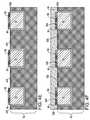
- FIGS. 1A-1Dare pictorial representations of a prior art interconnect structure at various stages of an EM failure.
- reference numeral 12denotes the dielectric cap
- reference numeral 10denotes the metal interconnect feature; all other components of the prior art interconnect structure are not labeled to avoid obscuring the EM problem.
- FIG. 1Ais at an initial stress stage.
- FIG. 1Bis at a time when void 14 nucleation initiates at the metal interconnect feature 10 /dielectric cap 12 interface.
- FIG. 1Cis at a time when the void 14 grows towards the bottom of the conductive feature 10
- FIG. 1Dis at a time in which the void 14 growth crosses the metal interconnect feature 10 causing a circuit dead opening.
- Prior art metal capsare typically comprised of a Co-containing alloy such as, for example, CoWP, which is selectively deposited atop of the Cu conductor region of the interconnect structure.
- CoWPCo-containing alloy
- One problem with utilizing such selective deposited metal capsis that some of the metal cap extends onto the adjoining surface of the interconnect dielectric material and, as such, electrical shorts between adjacent interconnects may arise. This is seen, for example, in FIG.
- reference numeral 20denotes a dielectric material
- reference numeral 22denotes a conductive material embedded within the dielectric material 20
- reference numeral 24denotes a Co-containing alloy metal cap
- reference numeral 25denotes metal residues from the Co-containing alloy cap process.
- the present inventionprovides a circuit interconnect structure that has improved EM reliability.
- the present inventionalso provides an interconnect structure in which electrical shorts between adjacent interconnect structures is avoided.
- the present inventionalso provides an interconnect structure that has better reliability and technology extendibility for the semiconductor industry.
- the present inventionprovides an interconnect structure in which a noble metal-containing cap layer is present directly on a non-recessed surface of a conductive material which is embedded within a low k dielectric material.
- low kis used throughout this application to denote an interconnect dielectric material having a dielectric constant of about 3.0 or less. Applicants have determined that by forming a hydrophobic surface layer within an exposed surface of a low k dielectric material prior to metal cap formation provides a means for controlling the selective formation of the metal cap directly on the non-recessed surface of a conductive material.
- the selective formation of the metal cap directly on the non-recessed surface of a conductive materialis enhanced since the formation rate of the metal cap on the non-recessed surface of a conductive material is greater than on the hydrophobic surface layer of the low k dielectric material.
- the interconnect structure of the present inventioncomprises:
- dielectric materialhaving a dielectric constant of about 3.0 or less, said dielectric material having a hydrophobic surface layer and at least one conductive material having an upper surface embedded within said dielectric material;
- a noble metal caplocated directly on said upper surface of said at least one conductive material, said noble metal cap does not substantially extend onto said hydrophobic surface layer of said dielectric material that is adjacent to said at least one conductive material and no noble metal residues are present on the hydrophobic surface layer of said dielectric material.
- the dielectric material which is present in the inventive interconnect structuremay be any interconnect dielectric material having a dielectric constant of about 3.0 or less.
- the dielectric material employed in the present inventioncomprises a silsesquioxane, a C doped oxide (i.e., an organosilicate) that includes at least atoms of Si, C, O and H, a thermosetting polyarylene ether, or multilayers thereof.
- the dielectric materialmay be porous, non-porous or contain regions and/or surfaces that are porous and other regions and/or surfaces that are non-porous.
- the hydrophobic surface layer that is present within the dielectric materialis formed in the present invention by treating the dielectric material with a hydrogen-containing plasma or, more preferably by thermal treatment in a hydrogen-containing ambient.
- the hydrophobic surface layerhas a depth, as measured from the top surface of the dielectric material into the interior of the dielectric material, of about 2 nm or less. Typically, the hydrophobic surface layer has a depth from about 1 to about 0.2 nm into the interior of the dielectric material.
- the conductive material which forms an embedded conductive region within the interconnect structureincludes any material that has the ability to transfer electricity.
- Examples of conductive material that can be present in the conductive regioninclude, for example, polySi, a conductive metal, a conductive metal alloy, a conductive metal silicide or combinations and multilayers thereof.
- the conductive materialincludes a conductive metal such as, for example, Cu, W, and/or Al.
- the conductive materialincludes a Cu-containing conductive material such as, for example, Cu, or a Cu alloy (such as AlCu).
- the conductive materialis typically separated from the dielectric material by a diffusion barrier.
- the diffusion barrierprevents diffusion of the conductive material into the dielectric material.
- Examples of diffusion barriers that can be present within the conductive regioninclude, for example, Ta, TaN, Ti, TiN, Ru, RuN, RuTa, RuTaN, IrTa, IrTaN, W, WN or combinations and multilayers thereof.
- the conductive materialmay be present within a via opening, a line opening, a combined via and line opening or any combination thereof.
- noble metalwhen referring to the cap located atop the at least one conductive material includes any metal that is resistant to corrosion or oxidation.
- the preferred noble metals that can be used in the present inventionare selected from the group consisting of Ru, Ir, Rh, Pt and alloys thereof. More preferably, the noble metal employed as the noble metal cap comprises Ru or a Ru alloy.
- the upper surface of the at least one conductive materialis substantially coplanar with the hydrophobic surface layer of the interconnect dielectric material. That is, the present invention provides structures in which the conductive material is non-recessed.
- the present inventionalso provides a method of fabricating the same.
- the applicantshave determined that improved selectivity of noble deposition onto the conductive material instead of the dielectric material can be obtained if the dielectric material including the embedded conductive material is treated to form a hydrophobic surface layer prior to the formation of the noble metal cap.
- the hydrophobic surface layercan be formed by treating the dielectric material with a hydrogen-containing plasma or, more preferably by thermal treatment in a hydrogen-containing ambient.
- the inventive methodincludes:
- dielectric materialhaving a dielectric constant of about 3.0 or less, said dielectric material having at least one conductive material having an upper surface embedded within said dielectric material;
- said noble metal capdirectly on said upper surface of said at least one conductive material, said noble metal cap does not substantially extend onto said hydrophobic surface layer that is adjacent to said at least one conductive material, said noble metal cap forming does not result in noble metal residues on the hydrophobic surface layer.
- FIGS. 1A-1Dare pictorial representations (through cross sectional views) illustrating the formation of a circuit dead opening in a prior art interconnect structure which is caused by EM failure.
- FIG. 2is a prior art interconnect structure including a Co-containing alloy metal cap located atop a conductive material that is embedded with a dielectric material, and metal residues from the Co-containing alloy cap process are present on the dielectric surface.
- FIG. 3is a pictorial representation of a prior art interconnect structure including a recessed conductive material embedded within a dielectric material.
- FIGS. 4A-4Fillustrate an interconnect structure through various processing steps of the present invention.
- the present inventionprovides an interconnect structure that includes a dielectric material having a dielectric constant of about 3.0 or less.
- This low k dielectric materialhas at least one conductive material having an upper surface embedded therein.
- the dielectric materialalso has a surface layer that is made hydrophobic prior to the formation of the noble metal cap.
- the noble metal capis located directly on the upper surface of the at least one conductive material. Because of the presence of the hydrophobic surface layer within the dielectric material, the noble metal cap does not substantially extend onto the hydrophobic surface layer that is adjacent to the at least one conductive material and no metal residues from the noble metal cap deposition form on this hydrophobic dielectric surface.
- the presentalso provides a method of fabricating such an interconnect structure in which exposed surfaces of a dielectric material including at least one conductive material embedded therein are made hydrophobic prior to the formation of the noble metal cap.
- the hydrophobic surface layer within the dielectric materialis achieved in the present invention by treating the dielectric material with a hydrogen-containing plasma or, more preferably by thermal treatment in a hydrogen-containing ambient. Such a treatment occurs after formation of the at least one conductive material embedded within the dielectric material, but prior to the formation of the noble metal cap.
- FIGS. 4A-4Fare pictorial representations (through cross sectional views) illustrating one exemplary interconnect structure of the present invention through various processing steps.
- FIG. 4Aillustrates an initial structure 50 that can be employed in the present invention in fabricating the inventive interconnect structure.
- the initial structure 50includes a dielectric material 52 having a pad stack 54 located on an upper surface thereof.
- the substratemay comprise a semiconducting material, an insulating material, a conductive material or any combination including multilayers thereof.
- any semiconductorsuch as Si, SiGe, SiGeC, SiC, Ge alloys, GaAs, InAs, InP and other III/V or II/VI compound semiconductors may be used.
- the present inventionalso contemplates cases in which the semiconductor substrate is a layered semiconductor such as, for example, Si/SiGe, Si/SiC, silicon-on-insulators (SOIs) or silicon germanium-on-insulators (SGOIs).
- the semiconductor substrateis a layered semiconductor such as, for example, Si/SiGe, Si/SiC, silicon-on-insulators (SOIs) or silicon germanium-on-insulators (SGOIs).
- the insulating materialcan be an organic insulator, an inorganic insulator or a combination thereof including multilayers.
- the substratemay include, for example, polySi, an elemental metal, alloys of elemental metals, a metal silicide, a metal nitride or combinations thereof including multilayers.
- the substratecomprises a semiconducting material, one or more semiconductor devices such as, for example, complementary metal oxide semiconductor (CMOS) devices can be fabricated thereon.
- CMOScomplementary metal oxide semiconductor
- the substratemay represent a first interconnect level of a multilayered interconnect structure.
- the dielectric material 52 of the initial structure 50comprises any interlevel or intralevel dielectric including inorganic dielectrics or organic dielectrics.
- the dielectric material 52may be porous, non-porous or contain regions and/or surfaces that are porous and other regions and/or surfaces that may be non-porous.
- suitable dielectricsinclude, but are not limited to: silsesquioxanes, C doped oxides (i.e., organosilicates) that include atoms of Si, C, O and H, thermosetting polyarylene ethers, or multilayers thereof.
- polyaryleneis used in this application to denote aryl moieties or inertly substituted aryl moieties which are linked together by bonds, fused rings, or inert linking groups such as, for example, oxygen, sulfur, sulfone, sulfoxide, carbonyl and the like.
- the dielectric material 52is formed utilizing any conventional deposition process including, but not limited to: chemical vapor deposition (CVD), plasma enhanced chemical vapor deposition (PECVD), evaporation, chemical solution deposition and spin-on coating.
- CVDchemical vapor deposition
- PECVDplasma enhanced chemical vapor deposition
- evaporationchemical solution deposition
- chemical solution depositionchemical solution deposition and spin-on coating.
- pad stack 54is formed on an exposed upper surface of dielectric material 52 .
- the pad stack 54comprises an oxide, nitride, oxynitride or multilayers thereof (e.g., a pad stack comprising a pad oxide and a pad nitride).
- the pad stack 54typically comprises a semiconductor oxide, semiconductor nitride and/or a semiconductor oxynitride.
- the pad stack 54comprises an oxide of silicon and/or a nitride of silicon.
- the pad stack 54may be formed utilizing any conventional deposition process including, for example, CVD, PECVD, evaporation, chemical solution deposition, physical vapor deposition (PVD) and atomic layer deposition.
- the pad stack 54is formed by a thermal process such as, for example, a thermal oxidation, a thermal nitridation and/or a thermal oxynitridation process.
- the pad stack 54is formed utilizing a combination of deposition and thermal processes.
- the thickness of the pad stack 54may vary depending on the number of materials within the pad stack itself as well as the technique that was used in forming the same. Typically, the pad stack 54 has a thickness from about 10 to about 80 nm.
- At least one opening 56is formed into the dielectric material 52 utilizing the pad stack 54 as a pattern mask.
- the resultant structure including the at least one opening 56is shown, for example, in FIG. 4B .
- the at least one opening 56may include a via opening, a line opening, a combined via and line opening, or any combinations thereof. In the drawings, three line openings are shown by way of a non-limiting example.
- the at least one opening 56is formed utilizing conventional lithography and etching.
- the lithographic stepincludes forming a photoresist (organic, inorganic or hybrid) atop the pad stack 54 utilizing a conventional deposition process such as, for example, CVD, PECVD and spin-on coating. Following formation of the photoresist, the photoresist is exposed to a desired pattern of radiation. Next, the exposed photoresist is developed utilizing a conventional resist development process.
- an etching stepis performed to transfer the pattern from the patterned photoresist into first the pad stack 54 and then the dielectric material 52 .
- the patterned photoresistis typically removed from the surface of the structure after transferring the pattern into the pad stack 54 utilizing a conventional resist stripping process such as, for example, ashing.
- the etching step used in forming the at least one opening 56comprises a dry etching process (including reactive ion etching, ion beam etching, plasma etching or laser ablation), a wet chemical etching process or any combination thereof. Typically, reactive ion etching is used to form the at least one opening 56 .
- the diffusion barrier 58comprises Ta, TaN, Ti, TiN, Ru, RuN, RuTa, RuTaN, IrTa, IrTaN, W, WN or any other material that can serve as a barrier to prevent conductive material from diffusing there through.
- the thickness of the diffusion barrier 58may vary depending on the deposition process used as well as the material employed. Typically, the diffusion barrier 58 has a thickness from about 4 to about 40 nm, with a thickness from about 7 to about 20 nm being more typical.
- the conductive material 60 used in forming the conductive region of the interconnect structureincludes, for example, polySi, a conductive metal, an alloy comprising at least one conductive metal, a conductive metal silicide or combinations thereof.
- the conductive material 60 that is used in forming the conductive regionis a conductive metal such as Cu, W or Al, with Cu or a Cu alloy (such as AlCu) being highly preferred in the present invention.
- the conductive material 60is formed into each of the openings 56 that are lined with the diffusion barrier 58 utilizing any conventional deposition process including, for example, CVD, PECVD, PVD, sputtering, plating, chemical solution deposition and electroless plating.
- a planarization processsuch as, for example, chemical mechanical polishing (CMP) and/or grinding.
- CMPchemical mechanical polishing
- the planarization processprovides a planar structure such as is shown in FIG. 4C in which the upper surfaces of the dielectric material 52 , the diffusion barrier 58 and the conductive material 60 are substantially coplanar with each other. It is noted that during the planarization process, the remaining pad stack 54 is removed from the structure.
- oxide and organic particleswhich are resulted from CMP slurry, denoted as reference numeral 61 can be formed on the surface of the conductive material.
- the presence of oxide and organic particles 61is undesirable in an interconnect structure since the same may degrade the adhesion between conductive material 60 and the capping layer 62 , FIG. 4E .
- Good adhesion between the conductive material 60 and the capping layer 62is required for good electromigration resistance.
- the presence of oxide and organic particles 61are undesirable in an interconnect structure since the same may degrade the selectivity of noble cap deposition between the conductive material 60 surface and the dielectric material 52 surface. For improved selectivity, a clean conductive material 60 surface is required.
- the surface (designed by reference numeral 52 A) of the dielectric material 52is hydrophilic at this point of the present invention.
- the oxide and organic particles 61can be removed from the surface of the conductive material 60 at the same time as creating a hydrophobic surface layer 52 B within the exposed portions of the dielectric material 52 not including conductive material 60 or diffusion barrier 58 .
- the hydrophobic surface layer 52 B that is present in the dielectric material 52is formed in the present invention by treating the dielectric material 52 with a hydrogen-containing plasma or, more preferably by thermal treatment in a hydrogen-containing ambient. Details concerning each of these treatments will be provided herein below.
- the hydrophobic surface layer 52 Bhas a depth as measured from the top surface of the dielectric material 52 into the interior of the dielectric material, of about 2 nm or less. Typically, the hydrophobic surface layer 52 B has a depth from about 1 to about 0.2 nm into the interior of the dielectric material.
- any hydrogen-containing sourcecan be used in generating a plasma including hydrogen.
- hydrogen-containing sourcesinclude, but are not limited to NH 3 and H 2 .
- the hydrogen-containing sourcemay be used alone or admixed with an inert gas such as, for example, He, Ar, Ne and mixtures thereof.
- the hydrogen-containing plasmamay contain a plasma including 100% hydrogen or the hydrogen content in the plasma may be in a range from about 2% up to 100% hydrogen.
- Plasma treatmentis performed at a temperature from about 100 to about 450° C., with a temperature from about 150 to about 300° C. being more preferred.
- the duration of plasma treatmentmay vary depending on the dielectric material being treated. Typically, plasma treatment is performed for a time period from about 10 seconds to about 5 minutes, with a duration of plasma treatment from about 30 seconds to about 2 minutes being more preferred.
- any hydrogen-containing sourcecan be used.
- hydrogen-containing sourcesinclude, but are not limited to NH 3 and H 2 .
- the hydrogen-containing sourcemay be used alone or admixed with an inert gas such as, for example, He, Ar, Ne and mixtures thereof.
- the hydrogen-containing ambientmay contain 100% hydrogen or the hydrogen may be in a range from about 2% up to 100% hydrogen.
- the hydrogenis preferably contained in an amount of from about 2% to about 90%, with a hydrogen content of from about 20% to about 70% being more typical.
- Thermal treating in a hydrogen-containing treatmentis performed at a temperature from about 100 to about 450° C., with a temperature from about 150 to about 300° C. being more preferred.
- the duration of thermal treatmentmay vary depending on the dielectric material being treated.
- thermal treatment in a hydrogen-containing ambientis performed for a time period from about 10 seconds to about 5 minutes, with a duration of thermal treatment from about 30 seconds to about 2 minutes being more preferred.
- a noble metal cap 62is selectively formed atop the conductive material 60 ; some of the noble metal cap 62 may extend onto the surface of the diffusion barrier 58 , but little or none of the noble metal cap 62 extends onto the hydrophobic surface layer 52 B of the dielectric material 52 that is laterally adjacent to said conductive material 60 . None of the noble metal cap 62 (or residues thereof) are deposited (or form) on the dielectric material 52 surface.
- the term “noble metal” when referring to the cap 62 located atop the at least one conductive region (i.e., conductive material 60 )includes any metal that is resistant to corrosion or oxidation.
- the preferred noble metals that can be used in the present inventionare selected from the group consisting of Ru, Ir, Rh, Pt and alloys thereof. More preferably, the noble metal employed as the noble metal cap comprises Ru or a Ru alloy. In some embodiments, the noble metal cap 62 is comprised of a multilayered noble metal or noble metal alloy stack.
- the thickness of the noble metal cap 62may vary depending on the type of noble metal present in the cap, the deposition technique and conditions used as well as the number of noble metals within the cap. Typically, the noble metal cap 62 has a thickness from about 1 to about 100 ⁇ , with a thickness from about 5 to about 50 ⁇ being more highly preferred.
- the noble metal cap 62is formed utilizing a low temperature deposition process including, for example, CVD, PECVD, low pressure CVD and ALD.
- low temperatureit is meant a deposition temperature of about 300° C. or less, with a deposition temperature between 150° C. and 250° C. being even more preferred.
- a dielectric capping layer 64is formed across the entire structure shown in FIG. 4E .
- the resultant structure including the dielectric capping layer 64is shown, for example, in FIG. 4F .
- the dielectric capping layer 64comprises any suitable dielectric capping material such as, for example, SiC, Si 4 NH 3 , SiO 2 , a carbon doped oxide, a nitrogen and hydrogen doped silicon carbide SiC(N,H) or multilayers thereof.
- the thickness of the dielectric capping layer 64may vary depending on the technique used to form the same as well as the material make-up of the layer. Typically, the dielectric capping layer 64 has a thickness from about 15 to about 100 nm, with a thickness from about 25 to about 45 nm being more typical.
- the dielectric capping layer 64is formed utilizing any conventional deposition process including, for example, CVD, PECVD, evaporation, spin-on coating, chemical solution deposition and PVD.
Landscapes
- Engineering & Computer Science (AREA)
- Physics & Mathematics (AREA)
- Condensed Matter Physics & Semiconductors (AREA)
- General Physics & Mathematics (AREA)
- Computer Hardware Design (AREA)
- Microelectronics & Electronic Packaging (AREA)
- Power Engineering (AREA)
- Manufacturing & Machinery (AREA)
- Plasma & Fusion (AREA)
- Internal Circuitry In Semiconductor Integrated Circuit Devices (AREA)
Abstract
Description
Claims (15)
Priority Applications (7)
| Application Number | Priority Date | Filing Date | Title |
|---|---|---|---|
| US12/021,316US7998864B2 (en) | 2008-01-29 | 2008-01-29 | Noble metal cap for interconnect structures |
| TW098101998ATW200952118A (en) | 2008-01-29 | 2009-01-20 | Noble metal cap for interconnect structures |
| JP2010544416AJP5441926B2 (en) | 2008-01-29 | 2009-01-22 | Noble metal cap for interconnect structure and method of forming the same (noble metal cap for interconnect structure) |
| KR1020107014649AKR20100098673A (en) | 2008-01-29 | 2009-01-22 | Noble metal cap for interconnect structures |
| PCT/US2009/031700WO2009097214A1 (en) | 2008-01-29 | 2009-01-22 | Noble metal cap for interconnect structures |
| EP09705024AEP2243155A4 (en) | 2008-01-29 | 2009-01-22 | Noble metal cap for interconnect structures |
| US13/191,090US8497580B2 (en) | 2008-01-29 | 2011-07-26 | Noble metal cap for interconnect structures |
Applications Claiming Priority (1)
| Application Number | Priority Date | Filing Date | Title |
|---|---|---|---|
| US12/021,316US7998864B2 (en) | 2008-01-29 | 2008-01-29 | Noble metal cap for interconnect structures |
Related Child Applications (1)
| Application Number | Title | Priority Date | Filing Date |
|---|---|---|---|
| US13/191,090DivisionUS8497580B2 (en) | 2008-01-29 | 2011-07-26 | Noble metal cap for interconnect structures |
Publications (2)
| Publication Number | Publication Date |
|---|---|
| US20090189287A1 US20090189287A1 (en) | 2009-07-30 |
| US7998864B2true US7998864B2 (en) | 2011-08-16 |
Family
ID=40898381
Family Applications (2)
| Application Number | Title | Priority Date | Filing Date |
|---|---|---|---|
| US12/021,316Expired - Fee RelatedUS7998864B2 (en) | 2008-01-29 | 2008-01-29 | Noble metal cap for interconnect structures |
| US13/191,090Active2028-02-11US8497580B2 (en) | 2008-01-29 | 2011-07-26 | Noble metal cap for interconnect structures |
Family Applications After (1)
| Application Number | Title | Priority Date | Filing Date |
|---|---|---|---|
| US13/191,090Active2028-02-11US8497580B2 (en) | 2008-01-29 | 2011-07-26 | Noble metal cap for interconnect structures |
Country Status (6)
| Country | Link |
|---|---|
| US (2) | US7998864B2 (en) |
| EP (1) | EP2243155A4 (en) |
| JP (1) | JP5441926B2 (en) |
| KR (1) | KR20100098673A (en) |
| TW (1) | TW200952118A (en) |
| WO (1) | WO2009097214A1 (en) |
Cited By (6)
| Publication number | Priority date | Publication date | Assignee | Title |
|---|---|---|---|---|
| US20120094469A1 (en)* | 2010-10-14 | 2012-04-19 | Didier Landru | Process for realising a connecting structure |
| US8796853B2 (en) | 2012-02-24 | 2014-08-05 | International Business Machines Corporation | Metallic capped interconnect structure with high electromigration resistance and low resistivity |
| US9059257B2 (en) | 2013-09-30 | 2015-06-16 | International Business Machines Corporation | Self-aligned vias formed using sacrificial metal caps |
| US9142456B2 (en) | 2013-07-30 | 2015-09-22 | Lam Research Corporation | Method for capping copper interconnect lines |
| US10643890B2 (en) | 2014-06-08 | 2020-05-05 | International Business Machines Corporation | Ultrathin multilayer metal alloy liner for nano Cu interconnects |
| US11289375B2 (en) | 2020-03-23 | 2022-03-29 | International Business Machines Corporation | Fully aligned interconnects with selective area deposition |
Families Citing this family (93)
| Publication number | Priority date | Publication date | Assignee | Title |
|---|---|---|---|---|
| US7830010B2 (en)* | 2008-04-03 | 2010-11-09 | International Business Machines Corporation | Surface treatment for selective metal cap applications |
| US8242019B2 (en)* | 2009-03-31 | 2012-08-14 | Tokyo Electron Limited | Selective deposition of metal-containing cap layers for semiconductor devices |
| US8178439B2 (en) | 2010-03-30 | 2012-05-15 | Tokyo Electron Limited | Surface cleaning and selective deposition of metal-containing cap layers for semiconductor devices |
| US8809183B2 (en) | 2010-09-21 | 2014-08-19 | International Business Machines Corporation | Interconnect structure with a planar interface between a selective conductive cap and a dielectric cap layer |
| US8912658B2 (en) | 2010-10-29 | 2014-12-16 | International Business Machines Corporation | Interconnect structure with enhanced reliability |
| US10283321B2 (en) | 2011-01-18 | 2019-05-07 | Applied Materials, Inc. | Semiconductor processing system and methods using capacitively coupled plasma |
| US8232200B1 (en)* | 2011-03-18 | 2012-07-31 | International Business Machines Corporation | Methods of forming integrated circuit devices having damascene interconnects therein with metal diffusion barrier layers and devices formed thereby |
| JP5862353B2 (en)* | 2011-08-05 | 2016-02-16 | 東京エレクトロン株式会社 | Manufacturing method of semiconductor device |
| WO2013070931A1 (en)* | 2011-11-08 | 2013-05-16 | Northeastern University | Damascene template for directed assembly and transfer of nanoelements |
| US9132436B2 (en) | 2012-09-21 | 2015-09-15 | Applied Materials, Inc. | Chemical control features in wafer process equipment |
| US9123726B2 (en)* | 2013-01-18 | 2015-09-01 | International Business Machines Corporation | Selective local metal cap layer formation for improved electromigration behavior |
| US9076847B2 (en) | 2013-01-18 | 2015-07-07 | International Business Machines Corporation | Selective local metal cap layer formation for improved electromigration behavior |
| US10256079B2 (en) | 2013-02-08 | 2019-04-09 | Applied Materials, Inc. | Semiconductor processing systems having multiple plasma configurations |
| US9362130B2 (en) | 2013-03-01 | 2016-06-07 | Applied Materials, Inc. | Enhanced etching processes using remote plasma sources |
| US9252049B2 (en)* | 2013-03-06 | 2016-02-02 | Taiwan Semiconductor Manufacturing Company, Ltd. | Method for forming interconnect structure that avoids via recess |
| WO2014189671A1 (en) | 2013-05-24 | 2014-11-27 | Applied Materials, Inc. | Cobalt selectivity improvement in selective cobalt process sequence |
| US20150206798A1 (en)* | 2014-01-17 | 2015-07-23 | Taiwan Semiconductor Manufacturing Company, Ltd. | Interconnect Structure And Method of Forming |
| US9309598B2 (en) | 2014-05-28 | 2016-04-12 | Applied Materials, Inc. | Oxide and metal removal |
| US9355922B2 (en) | 2014-10-14 | 2016-05-31 | Applied Materials, Inc. | Systems and methods for internal surface conditioning in plasma processing equipment |
| US9966240B2 (en) | 2014-10-14 | 2018-05-08 | Applied Materials, Inc. | Systems and methods for internal surface conditioning assessment in plasma processing equipment |
| US11637002B2 (en) | 2014-11-26 | 2023-04-25 | Applied Materials, Inc. | Methods and systems to enhance process uniformity |
| US10224210B2 (en) | 2014-12-09 | 2019-03-05 | Applied Materials, Inc. | Plasma processing system with direct outlet toroidal plasma source |
| US11257693B2 (en) | 2015-01-09 | 2022-02-22 | Applied Materials, Inc. | Methods and systems to improve pedestal temperature control |
| US20160225652A1 (en) | 2015-02-03 | 2016-08-04 | Applied Materials, Inc. | Low temperature chuck for plasma processing systems |
| US9728437B2 (en) | 2015-02-03 | 2017-08-08 | Applied Materials, Inc. | High temperature chuck for plasma processing systems |
| US9741593B2 (en) | 2015-08-06 | 2017-08-22 | Applied Materials, Inc. | Thermal management systems and methods for wafer processing systems |
| US9691645B2 (en) | 2015-08-06 | 2017-06-27 | Applied Materials, Inc. | Bolted wafer chuck thermal management systems and methods for wafer processing systems |
| US9349605B1 (en) | 2015-08-07 | 2016-05-24 | Applied Materials, Inc. | Oxide etch selectivity systems and methods |
| US10504700B2 (en) | 2015-08-27 | 2019-12-10 | Applied Materials, Inc. | Plasma etching systems and methods with secondary plasma injection |
| US10014213B2 (en) | 2015-10-15 | 2018-07-03 | Tokyo Electron Limited | Selective bottom-up metal feature filling for interconnects |
| US10504754B2 (en) | 2016-05-19 | 2019-12-10 | Applied Materials, Inc. | Systems and methods for improved semiconductor etching and component protection |
| US10522371B2 (en) | 2016-05-19 | 2019-12-31 | Applied Materials, Inc. | Systems and methods for improved semiconductor etching and component protection |
| US9865484B1 (en) | 2016-06-29 | 2018-01-09 | Applied Materials, Inc. | Selective etch using material modification and RF pulsing |
| US9911698B1 (en)* | 2016-08-25 | 2018-03-06 | International Business Machines Corporation | Metal alloy capping layers for metallic interconnect structures |
| US10629473B2 (en) | 2016-09-09 | 2020-04-21 | Applied Materials, Inc. | Footing removal for nitride spacer |
| US10062575B2 (en) | 2016-09-09 | 2018-08-28 | Applied Materials, Inc. | Poly directional etch by oxidation |
| US10546729B2 (en) | 2016-10-04 | 2020-01-28 | Applied Materials, Inc. | Dual-channel showerhead with improved profile |
| US9934942B1 (en) | 2016-10-04 | 2018-04-03 | Applied Materials, Inc. | Chamber with flow-through source |
| US10062579B2 (en) | 2016-10-07 | 2018-08-28 | Applied Materials, Inc. | Selective SiN lateral recess |
| US10163696B2 (en) | 2016-11-11 | 2018-12-25 | Applied Materials, Inc. | Selective cobalt removal for bottom up gapfill |
| US9768034B1 (en) | 2016-11-11 | 2017-09-19 | Applied Materials, Inc. | Removal methods for high aspect ratio structures |
| US10242908B2 (en) | 2016-11-14 | 2019-03-26 | Applied Materials, Inc. | Airgap formation with damage-free copper |
| US10026621B2 (en) | 2016-11-14 | 2018-07-17 | Applied Materials, Inc. | SiN spacer profile patterning |
| US10566206B2 (en) | 2016-12-27 | 2020-02-18 | Applied Materials, Inc. | Systems and methods for anisotropic material breakthrough |
| US10403507B2 (en) | 2017-02-03 | 2019-09-03 | Applied Materials, Inc. | Shaped etch profile with oxidation |
| US10431429B2 (en) | 2017-02-03 | 2019-10-01 | Applied Materials, Inc. | Systems and methods for radial and azimuthal control of plasma uniformity |
| US10319739B2 (en) | 2017-02-08 | 2019-06-11 | Applied Materials, Inc. | Accommodating imperfectly aligned memory holes |
| WO2018148659A1 (en) | 2017-02-10 | 2018-08-16 | Northeastern University | Damascene template for nanoelement printing fabricated without chemomechanical planarizaton |
| US10943834B2 (en) | 2017-03-13 | 2021-03-09 | Applied Materials, Inc. | Replacement contact process |
| US10319649B2 (en) | 2017-04-11 | 2019-06-11 | Applied Materials, Inc. | Optical emission spectroscopy (OES) for remote plasma monitoring |
| US11276590B2 (en) | 2017-05-17 | 2022-03-15 | Applied Materials, Inc. | Multi-zone semiconductor substrate supports |
| US11276559B2 (en) | 2017-05-17 | 2022-03-15 | Applied Materials, Inc. | Semiconductor processing chamber for multiple precursor flow |
| JP7176860B6 (en) | 2017-05-17 | 2022-12-16 | アプライド マテリアルズ インコーポレイテッド | Semiconductor processing chamber to improve precursor flow |
| US10497579B2 (en) | 2017-05-31 | 2019-12-03 | Applied Materials, Inc. | Water-free etching methods |
| US10049891B1 (en) | 2017-05-31 | 2018-08-14 | Applied Materials, Inc. | Selective in situ cobalt residue removal |
| US10920320B2 (en) | 2017-06-16 | 2021-02-16 | Applied Materials, Inc. | Plasma health determination in semiconductor substrate processing reactors |
| US10541246B2 (en) | 2017-06-26 | 2020-01-21 | Applied Materials, Inc. | 3D flash memory cells which discourage cross-cell electrical tunneling |
| US10727080B2 (en) | 2017-07-07 | 2020-07-28 | Applied Materials, Inc. | Tantalum-containing material removal |
| US10541184B2 (en) | 2017-07-11 | 2020-01-21 | Applied Materials, Inc. | Optical emission spectroscopic techniques for monitoring etching |
| US10354889B2 (en)* | 2017-07-17 | 2019-07-16 | Applied Materials, Inc. | Non-halogen etching of silicon-containing materials |
| US10043674B1 (en) | 2017-08-04 | 2018-08-07 | Applied Materials, Inc. | Germanium etching systems and methods |
| US10170336B1 (en) | 2017-08-04 | 2019-01-01 | Applied Materials, Inc. | Methods for anisotropic control of selective silicon removal |
| US10297458B2 (en) | 2017-08-07 | 2019-05-21 | Applied Materials, Inc. | Process window widening using coated parts in plasma etch processes |
| US10128086B1 (en) | 2017-10-24 | 2018-11-13 | Applied Materials, Inc. | Silicon pretreatment for nitride removal |
| US10424487B2 (en) | 2017-10-24 | 2019-09-24 | Applied Materials, Inc. | Atomic layer etching processes |
| US10283324B1 (en) | 2017-10-24 | 2019-05-07 | Applied Materials, Inc. | Oxygen treatment for nitride etching |
| US10256112B1 (en) | 2017-12-08 | 2019-04-09 | Applied Materials, Inc. | Selective tungsten removal |
| US10903054B2 (en) | 2017-12-19 | 2021-01-26 | Applied Materials, Inc. | Multi-zone gas distribution systems and methods |
| US11328909B2 (en) | 2017-12-22 | 2022-05-10 | Applied Materials, Inc. | Chamber conditioning and removal processes |
| US10854426B2 (en) | 2018-01-08 | 2020-12-01 | Applied Materials, Inc. | Metal recess for semiconductor structures |
| US10964512B2 (en) | 2018-02-15 | 2021-03-30 | Applied Materials, Inc. | Semiconductor processing chamber multistage mixing apparatus and methods |
| US10679870B2 (en) | 2018-02-15 | 2020-06-09 | Applied Materials, Inc. | Semiconductor processing chamber multistage mixing apparatus |
| TWI766433B (en) | 2018-02-28 | 2022-06-01 | 美商應用材料股份有限公司 | Systems and methods to form airgaps |
| US10593560B2 (en) | 2018-03-01 | 2020-03-17 | Applied Materials, Inc. | Magnetic induction plasma source for semiconductor processes and equipment |
| US10319600B1 (en) | 2018-03-12 | 2019-06-11 | Applied Materials, Inc. | Thermal silicon etch |
| US10497573B2 (en) | 2018-03-13 | 2019-12-03 | Applied Materials, Inc. | Selective atomic layer etching of semiconductor materials |
| US10573527B2 (en) | 2018-04-06 | 2020-02-25 | Applied Materials, Inc. | Gas-phase selective etching systems and methods |
| US10490406B2 (en) | 2018-04-10 | 2019-11-26 | Appled Materials, Inc. | Systems and methods for material breakthrough |
| US10699879B2 (en) | 2018-04-17 | 2020-06-30 | Applied Materials, Inc. | Two piece electrode assembly with gap for plasma control |
| US10886137B2 (en) | 2018-04-30 | 2021-01-05 | Applied Materials, Inc. | Selective nitride removal |
| US10872778B2 (en) | 2018-07-06 | 2020-12-22 | Applied Materials, Inc. | Systems and methods utilizing solid-phase etchants |
| US10755941B2 (en) | 2018-07-06 | 2020-08-25 | Applied Materials, Inc. | Self-limiting selective etching systems and methods |
| US10672642B2 (en) | 2018-07-24 | 2020-06-02 | Applied Materials, Inc. | Systems and methods for pedestal configuration |
| US11049755B2 (en) | 2018-09-14 | 2021-06-29 | Applied Materials, Inc. | Semiconductor substrate supports with embedded RF shield |
| US10892198B2 (en) | 2018-09-14 | 2021-01-12 | Applied Materials, Inc. | Systems and methods for improved performance in semiconductor processing |
| US11062887B2 (en) | 2018-09-17 | 2021-07-13 | Applied Materials, Inc. | High temperature RF heater pedestals |
| US11417534B2 (en) | 2018-09-21 | 2022-08-16 | Applied Materials, Inc. | Selective material removal |
| US11682560B2 (en) | 2018-10-11 | 2023-06-20 | Applied Materials, Inc. | Systems and methods for hafnium-containing film removal |
| US11121002B2 (en) | 2018-10-24 | 2021-09-14 | Applied Materials, Inc. | Systems and methods for etching metals and metal derivatives |
| US11437242B2 (en) | 2018-11-27 | 2022-09-06 | Applied Materials, Inc. | Selective removal of silicon-containing materials |
| US11721527B2 (en) | 2019-01-07 | 2023-08-08 | Applied Materials, Inc. | Processing chamber mixing systems |
| US10920319B2 (en) | 2019-01-11 | 2021-02-16 | Applied Materials, Inc. | Ceramic showerheads with conductive electrodes |
| US12341100B2 (en)* | 2021-10-11 | 2025-06-24 | International Business Machines Corporation | Copper interconnects with self-aligned hourglass-shaped metal cap |
Citations (11)
| Publication number | Priority date | Publication date | Assignee | Title |
|---|---|---|---|---|
| US5585673A (en) | 1992-02-26 | 1996-12-17 | International Business Machines Corporation | Refractory metal capped low resistivity metal conductor lines and vias |
| US5695810A (en) | 1996-11-20 | 1997-12-09 | Cornell Research Foundation, Inc. | Use of cobalt tungsten phosphide as a barrier material for copper metallization |
| US6342733B1 (en) | 1999-07-27 | 2002-01-29 | International Business Machines Corporation | Reduced electromigration and stressed induced migration of Cu wires by surface coating |
| US6706625B1 (en) | 2002-12-06 | 2004-03-16 | Chartered Semiconductor Manufacturing Ltd. | Copper recess formation using chemical process for fabricating barrier cap for lines and vias |
| US20040113279A1 (en) | 2002-12-16 | 2004-06-17 | International Business Machines Corporation | Copper recess process with application to selective capping and electroless plating |
| US6881437B2 (en)* | 2003-06-16 | 2005-04-19 | Blue29 Llc | Methods and system for processing a microelectronic topography |
| US20050085031A1 (en) | 2003-10-15 | 2005-04-21 | Applied Materials, Inc. | Heterogeneous activation layers formed by ionic and electroless reactions used for IC interconnect capping layers |
| US20060189133A1 (en) | 2005-02-22 | 2006-08-24 | International Business Machines Corporation | Reliable BEOL integration process with direct CMP of porous SiCOH dielectric |
| US7105445B2 (en) | 2005-01-14 | 2006-09-12 | International Business Machines Corporation | Interconnect structures with encasing cap and methods of making thereof |
| WO2007003223A1 (en) | 2005-07-04 | 2007-01-11 | Freescale Semiconductor, Inc. | Method and apparatus for forming a noble metal layer, notably on inlaid metal features |
| US20070077750A1 (en) | 2005-09-06 | 2007-04-05 | Paul Ma | Atomic layer deposition processes for ruthenium materials |
Family Cites Families (10)
| Publication number | Priority date | Publication date | Assignee | Title |
|---|---|---|---|---|
| JP4119542B2 (en)* | 1998-09-29 | 2008-07-16 | 松下電器産業株式会社 | Method for manufacturing semiconductor device and method for forming insulating film |
| JP2002353308A (en)* | 2001-05-28 | 2002-12-06 | Toshiba Corp | Semiconductor device and manufacturing method thereof |
| KR100519169B1 (en)* | 2003-05-09 | 2005-10-06 | 매그나칩 반도체 유한회사 | Method of forming metal line of semiconductor devices |
| JP2005056945A (en)* | 2003-08-08 | 2005-03-03 | Hitachi Ltd | Method of manufacturing semiconductor device |
| US7476618B2 (en)* | 2004-10-26 | 2009-01-13 | Asm Japan K.K. | Selective formation of metal layers in an integrated circuit |
| US20060113675A1 (en)* | 2004-12-01 | 2006-06-01 | Chung-Liang Chang | Barrier material and process for Cu interconnect |
| US7273814B2 (en)* | 2005-03-16 | 2007-09-25 | Tokyo Electron Limited | Method for forming a ruthenium metal layer on a patterned substrate |
| US7084060B1 (en)* | 2005-05-04 | 2006-08-01 | International Business Machines Corporation | Forming capping layer over metal wire structure using selective atomic layer deposition |
| CN101326630B (en)* | 2005-12-07 | 2011-07-20 | Nxp股份有限公司 | A method of forming a layer over a surface of a first material embedded in a second material in a structure for a semiconductor device |
| US8138604B2 (en)* | 2007-06-21 | 2012-03-20 | International Business Machines Corporation | Metal cap with ultra-low k dielectric material for circuit interconnect applications |
- 2008
- 2008-01-29USUS12/021,316patent/US7998864B2/ennot_activeExpired - Fee Related
- 2009
- 2009-01-20TWTW098101998Apatent/TW200952118A/enunknown
- 2009-01-22JPJP2010544416Apatent/JP5441926B2/ennot_activeExpired - Fee Related
- 2009-01-22KRKR1020107014649Apatent/KR20100098673A/ennot_activeAbandoned
- 2009-01-22EPEP09705024Apatent/EP2243155A4/ennot_activeWithdrawn
- 2009-01-22WOPCT/US2009/031700patent/WO2009097214A1/enactiveApplication Filing
- 2011
- 2011-07-26USUS13/191,090patent/US8497580B2/enactiveActive
Patent Citations (12)
| Publication number | Priority date | Publication date | Assignee | Title |
|---|---|---|---|---|
| US5585673A (en) | 1992-02-26 | 1996-12-17 | International Business Machines Corporation | Refractory metal capped low resistivity metal conductor lines and vias |
| US6323554B1 (en) | 1992-02-26 | 2001-11-27 | International Business Machines Corporation | Refractory metal capped low resistivity metal conductor lines and vias formed using PVD and CVD |
| US5695810A (en) | 1996-11-20 | 1997-12-09 | Cornell Research Foundation, Inc. | Use of cobalt tungsten phosphide as a barrier material for copper metallization |
| US6342733B1 (en) | 1999-07-27 | 2002-01-29 | International Business Machines Corporation | Reduced electromigration and stressed induced migration of Cu wires by surface coating |
| US6706625B1 (en) | 2002-12-06 | 2004-03-16 | Chartered Semiconductor Manufacturing Ltd. | Copper recess formation using chemical process for fabricating barrier cap for lines and vias |
| US20040113279A1 (en) | 2002-12-16 | 2004-06-17 | International Business Machines Corporation | Copper recess process with application to selective capping and electroless plating |
| US6881437B2 (en)* | 2003-06-16 | 2005-04-19 | Blue29 Llc | Methods and system for processing a microelectronic topography |
| US20050085031A1 (en) | 2003-10-15 | 2005-04-21 | Applied Materials, Inc. | Heterogeneous activation layers formed by ionic and electroless reactions used for IC interconnect capping layers |
| US7105445B2 (en) | 2005-01-14 | 2006-09-12 | International Business Machines Corporation | Interconnect structures with encasing cap and methods of making thereof |
| US20060189133A1 (en) | 2005-02-22 | 2006-08-24 | International Business Machines Corporation | Reliable BEOL integration process with direct CMP of porous SiCOH dielectric |
| WO2007003223A1 (en) | 2005-07-04 | 2007-01-11 | Freescale Semiconductor, Inc. | Method and apparatus for forming a noble metal layer, notably on inlaid metal features |
| US20070077750A1 (en) | 2005-09-06 | 2007-04-05 | Paul Ma | Atomic layer deposition processes for ruthenium materials |
Non-Patent Citations (2)
| Title |
|---|
| International Search Report dated Mar. 12, 2009. |
| U.S. Appl. No. 11/766,261 entitled "Metal Cap With Ultra-Low k Dielectric Material for Circuit Interconnect Applications," First Named Inventor: Chih-Chao Yang, filed on Jun. 21, 2007. |
Cited By (8)
| Publication number | Priority date | Publication date | Assignee | Title |
|---|---|---|---|---|
| US20120094469A1 (en)* | 2010-10-14 | 2012-04-19 | Didier Landru | Process for realising a connecting structure |
| US9224704B2 (en)* | 2010-10-14 | 2015-12-29 | Soitec | Process for realizing a connecting structure |
| US8796853B2 (en) | 2012-02-24 | 2014-08-05 | International Business Machines Corporation | Metallic capped interconnect structure with high electromigration resistance and low resistivity |
| US9142456B2 (en) | 2013-07-30 | 2015-09-22 | Lam Research Corporation | Method for capping copper interconnect lines |
| US9059257B2 (en) | 2013-09-30 | 2015-06-16 | International Business Machines Corporation | Self-aligned vias formed using sacrificial metal caps |
| US10643890B2 (en) | 2014-06-08 | 2020-05-05 | International Business Machines Corporation | Ultrathin multilayer metal alloy liner for nano Cu interconnects |
| US11177167B2 (en) | 2014-06-08 | 2021-11-16 | International Business Machines Corporation | Ultrathin multilayer metal alloy liner for nano Cu interconnects |
| US11289375B2 (en) | 2020-03-23 | 2022-03-29 | International Business Machines Corporation | Fully aligned interconnects with selective area deposition |
Also Published As
| Publication number | Publication date |
|---|---|
| US8497580B2 (en) | 2013-07-30 |
| KR20100098673A (en) | 2010-09-08 |
| US20090189287A1 (en) | 2009-07-30 |
| US20110285021A1 (en) | 2011-11-24 |
| EP2243155A4 (en) | 2012-07-25 |
| JP5441926B2 (en) | 2014-03-12 |
| TW200952118A (en) | 2009-12-16 |
| EP2243155A1 (en) | 2010-10-27 |
| WO2009097214A1 (en) | 2009-08-06 |
| JP2011511439A (en) | 2011-04-07 |
Similar Documents
| Publication | Publication Date | Title |
|---|---|---|
| US7998864B2 (en) | Noble metal cap for interconnect structures | |
| US8013446B2 (en) | Nitrogen-containing metal cap for interconnect structures | |
| US8669182B2 (en) | Metal cap with ultra-low κ dielectric material for circuit interconnect applications | |
| US8354751B2 (en) | Interconnect structure for electromigration enhancement | |
| US7834457B2 (en) | Bilayer metal capping layer for interconnect applications | |
| US8133767B2 (en) | Efficient interconnect structure for electrical fuse applications | |
| US8288276B2 (en) | Method of forming an interconnect structure including a metallic interfacial layer located at a bottom via portion | |
| US9006895B2 (en) | Interconnect structures containing nitrided metallic residues | |
| US8889546B2 (en) | Discontinuous/non-uniform metal cap structure and process for interconnect integration | |
| WO2011084667A2 (en) | Interconnect structure with a mushroom-shaped oxide capping layer and method for fabricating same | |
| US8802563B2 (en) | Surface repair structure and process for interconnect applications | |
| US20090072406A1 (en) | Interconnect structure with improved electromigration resistance and method of fabricating same | |
| US7687877B2 (en) | Interconnect structure with a mushroom-shaped oxide capping layer and method for fabricating same | |
| WO2010016958A1 (en) | Interconnect structure with metal cap self-aligned to a surface of an embedded conductive material |
Legal Events
| Date | Code | Title | Description |
|---|---|---|---|
| AS | Assignment | Owner name:INTERNATIONAL BUSINESS MACHINES CORPORATION, NEW Y Free format text:ASSIGNMENT OF ASSIGNORS INTEREST;ASSIGNORS:YANG, CHIH-CHAO;EDELSTEIN, DANIEL C.;MCFEELY, FENTON R.;REEL/FRAME:020430/0526;SIGNING DATES FROM 20080109 TO 20080120 Owner name:INTERNATIONAL BUSINESS MACHINES CORPORATION, NEW Y Free format text:ASSIGNMENT OF ASSIGNORS INTEREST;ASSIGNORS:YANG, CHIH-CHAO;EDELSTEIN, DANIEL C.;MCFEELY, FENTON R.;SIGNING DATES FROM 20080109 TO 20080120;REEL/FRAME:020430/0526 | |
| STCF | Information on status: patent grant | Free format text:PATENTED CASE | |
| REMI | Maintenance fee reminder mailed | ||
| FPAY | Fee payment | Year of fee payment:4 | |
| SULP | Surcharge for late payment | ||
| AS | Assignment | Owner name:GLOBALFOUNDRIES U.S. 2 LLC, NEW YORK Free format text:ASSIGNMENT OF ASSIGNORS INTEREST;ASSIGNOR:INTERNATIONAL BUSINESS MACHINES CORPORATION;REEL/FRAME:036550/0001 Effective date:20150629 | |
| AS | Assignment | Owner name:GLOBALFOUNDRIES INC., CAYMAN ISLANDS Free format text:ASSIGNMENT OF ASSIGNORS INTEREST;ASSIGNORS:GLOBALFOUNDRIES U.S. 2 LLC;GLOBALFOUNDRIES U.S. INC.;REEL/FRAME:036779/0001 Effective date:20150910 | |
| AS | Assignment | Owner name:WILMINGTON TRUST, NATIONAL ASSOCIATION, DELAWARE Free format text:SECURITY AGREEMENT;ASSIGNOR:GLOBALFOUNDRIES INC.;REEL/FRAME:049490/0001 Effective date:20181127 | |
| FEPP | Fee payment procedure | Free format text:MAINTENANCE FEE REMINDER MAILED (ORIGINAL EVENT CODE: REM.); ENTITY STATUS OF PATENT OWNER: LARGE ENTITY | |
| LAPS | Lapse for failure to pay maintenance fees | Free format text:PATENT EXPIRED FOR FAILURE TO PAY MAINTENANCE FEES (ORIGINAL EVENT CODE: EXP.); ENTITY STATUS OF PATENT OWNER: LARGE ENTITY | |
| STCH | Information on status: patent discontinuation | Free format text:PATENT EXPIRED DUE TO NONPAYMENT OF MAINTENANCE FEES UNDER 37 CFR 1.362 | |
| FP | Lapsed due to failure to pay maintenance fee | Effective date:20190816 | |
| AS | Assignment | Owner name:GLOBALFOUNDRIES INC., CAYMAN ISLANDS Free format text:RELEASE BY SECURED PARTY;ASSIGNOR:WILMINGTON TRUST, NATIONAL ASSOCIATION;REEL/FRAME:054636/0001 Effective date:20201117 | |
| AS | Assignment | Owner name:GLOBALFOUNDRIES U.S. INC., NEW YORK Free format text:RELEASE BY SECURED PARTY;ASSIGNOR:WILMINGTON TRUST, NATIONAL ASSOCIATION;REEL/FRAME:056987/0001 Effective date:20201117 |