US7996986B2 - Apparatus for forming magnetic recording heads - Google Patents
Apparatus for forming magnetic recording headsDownload PDFInfo
- Publication number
- US7996986B2 US7996986B2US12/370,976US37097609AUS7996986B2US 7996986 B2US7996986 B2US 7996986B2US 37097609 AUS37097609 AUS 37097609AUS 7996986 B2US7996986 B2US 7996986B2
- Authority
- US
- United States
- Prior art keywords
- lapping
- layer
- guides
- lapping guide
- guide
- Prior art date
- Legal status (The legal status is an assumption and is not a legal conclusion. Google has not performed a legal analysis and makes no representation as to the accuracy of the status listed.)
- Expired - Fee Related, expires
Links
Images


Classifications
- G—PHYSICS
- G11—INFORMATION STORAGE
- G11B—INFORMATION STORAGE BASED ON RELATIVE MOVEMENT BETWEEN RECORD CARRIER AND TRANSDUCER
- G11B5/00—Recording by magnetisation or demagnetisation of a record carrier; Reproducing by magnetic means; Record carriers therefor
- G11B5/127—Structure or manufacture of heads, e.g. inductive
- G11B5/31—Structure or manufacture of heads, e.g. inductive using thin films
- G11B5/3163—Fabrication methods or processes specially adapted for a particular head structure, e.g. using base layers for electroplating, using functional layers for masking, using energy or particle beams for shaping the structure or modifying the properties of the basic layers
- G11B5/3166—Testing or indicating in relation thereto, e.g. before the fabrication is completed
- G—PHYSICS
- G11—INFORMATION STORAGE
- G11B—INFORMATION STORAGE BASED ON RELATIVE MOVEMENT BETWEEN RECORD CARRIER AND TRANSDUCER
- G11B5/00—Recording by magnetisation or demagnetisation of a record carrier; Reproducing by magnetic means; Record carriers therefor
- G11B5/127—Structure or manufacture of heads, e.g. inductive
- G11B5/31—Structure or manufacture of heads, e.g. inductive using thin films
- G11B5/3109—Details
- G11B5/313—Disposition of layers
- G11B5/3133—Disposition of layers including layers not usually being a part of the electromagnetic transducer structure and providing additional features, e.g. for improving heat radiation, reduction of power dissipation, adaptations for measurement or indication of gap depth or other properties of the structure
- G11B5/314—Disposition of layers including layers not usually being a part of the electromagnetic transducer structure and providing additional features, e.g. for improving heat radiation, reduction of power dissipation, adaptations for measurement or indication of gap depth or other properties of the structure where the layers are extra layers normally not provided in the transducing structure, e.g. optical layers
- G—PHYSICS
- G11—INFORMATION STORAGE
- G11B—INFORMATION STORAGE BASED ON RELATIVE MOVEMENT BETWEEN RECORD CARRIER AND TRANSDUCER
- G11B5/00—Recording by magnetisation or demagnetisation of a record carrier; Reproducing by magnetic means; Record carriers therefor
- G11B5/127—Structure or manufacture of heads, e.g. inductive
- G11B5/31—Structure or manufacture of heads, e.g. inductive using thin films
- G11B5/3163—Fabrication methods or processes specially adapted for a particular head structure, e.g. using base layers for electroplating, using functional layers for masking, using energy or particle beams for shaping the structure or modifying the properties of the basic layers
- G11B5/3169—Working or finishing the interfacing surface of heads, e.g. lapping of heads
- G—PHYSICS
- G11—INFORMATION STORAGE
- G11B—INFORMATION STORAGE BASED ON RELATIVE MOVEMENT BETWEEN RECORD CARRIER AND TRANSDUCER
- G11B5/00—Recording by magnetisation or demagnetisation of a record carrier; Reproducing by magnetic means; Record carriers therefor
- G11B2005/0002—Special dispositions or recording techniques
- G11B2005/0005—Arrangements, methods or circuits
- G11B2005/0021—Thermally assisted recording using an auxiliary energy source for heating the recording layer locally to assist the magnetization reversal
- Y—GENERAL TAGGING OF NEW TECHNOLOGICAL DEVELOPMENTS; GENERAL TAGGING OF CROSS-SECTIONAL TECHNOLOGIES SPANNING OVER SEVERAL SECTIONS OF THE IPC; TECHNICAL SUBJECTS COVERED BY FORMER USPC CROSS-REFERENCE ART COLLECTIONS [XRACs] AND DIGESTS
- Y10—TECHNICAL SUBJECTS COVERED BY FORMER USPC
- Y10T—TECHNICAL SUBJECTS COVERED BY FORMER US CLASSIFICATION
- Y10T29/00—Metal working
- Y10T29/49—Method of mechanical manufacture
- Y10T29/49002—Electrical device making
- Y10T29/4902—Electromagnet, transformer or inductor
- Y10T29/49021—Magnetic recording reproducing transducer [e.g., tape head, core, etc.]
- Y10T29/49032—Fabricating head structure or component thereof
- Y10T29/49036—Fabricating head structure or component thereof including measuring or testing
- Y10T29/49043—Depositing magnetic layer or coating
- Y10T29/49044—Plural magnetic deposition layers
- Y—GENERAL TAGGING OF NEW TECHNOLOGICAL DEVELOPMENTS; GENERAL TAGGING OF CROSS-SECTIONAL TECHNOLOGIES SPANNING OVER SEVERAL SECTIONS OF THE IPC; TECHNICAL SUBJECTS COVERED BY FORMER USPC CROSS-REFERENCE ART COLLECTIONS [XRACs] AND DIGESTS
- Y10—TECHNICAL SUBJECTS COVERED BY FORMER USPC
- Y10T—TECHNICAL SUBJECTS COVERED BY FORMER US CLASSIFICATION
- Y10T29/00—Metal working
- Y10T29/49—Method of mechanical manufacture
- Y10T29/49002—Electrical device making
- Y10T29/4902—Electromagnet, transformer or inductor
- Y10T29/49021—Magnetic recording reproducing transducer [e.g., tape head, core, etc.]
- Y10T29/49032—Fabricating head structure or component thereof
- Y10T29/49036—Fabricating head structure or component thereof including measuring or testing
- Y10T29/49043—Depositing magnetic layer or coating
- Y10T29/49046—Depositing magnetic layer or coating with etching or machining of magnetic material
- Y—GENERAL TAGGING OF NEW TECHNOLOGICAL DEVELOPMENTS; GENERAL TAGGING OF CROSS-SECTIONAL TECHNOLOGIES SPANNING OVER SEVERAL SECTIONS OF THE IPC; TECHNICAL SUBJECTS COVERED BY FORMER USPC CROSS-REFERENCE ART COLLECTIONS [XRACs] AND DIGESTS
- Y10—TECHNICAL SUBJECTS COVERED BY FORMER USPC
- Y10T—TECHNICAL SUBJECTS COVERED BY FORMER US CLASSIFICATION
- Y10T29/00—Metal working
- Y10T29/49—Method of mechanical manufacture
- Y10T29/49002—Electrical device making
- Y10T29/4902—Electromagnet, transformer or inductor
- Y10T29/49021—Magnetic recording reproducing transducer [e.g., tape head, core, etc.]
- Y10T29/49032—Fabricating head structure or component thereof
- Y10T29/49048—Machining magnetic material [e.g., grinding, etching, polishing]
- Y10T29/49052—Machining magnetic material [e.g., grinding, etching, polishing] by etching
- Y—GENERAL TAGGING OF NEW TECHNOLOGICAL DEVELOPMENTS; GENERAL TAGGING OF CROSS-SECTIONAL TECHNOLOGIES SPANNING OVER SEVERAL SECTIONS OF THE IPC; TECHNICAL SUBJECTS COVERED BY FORMER USPC CROSS-REFERENCE ART COLLECTIONS [XRACs] AND DIGESTS
- Y10—TECHNICAL SUBJECTS COVERED BY FORMER USPC
- Y10T—TECHNICAL SUBJECTS COVERED BY FORMER US CLASSIFICATION
- Y10T29/00—Metal working
- Y10T29/53—Means to assemble or disassemble
- Y10T29/5313—Means to assemble electrical device
- Y10T29/53165—Magnetic memory device
Definitions
- a plurality of transducers and auxiliary circuitsare typically fabricated on a common substrate.
- features of the magnetic headsuch as the height of a magnetoresistive element (MRE) sensor or a throat height of a write pole are controlled within a very tight tolerance.
- MREmagnetoresistive element
- Thin film deposition techniquesare often used to fabricate magnetic read/write transducers.
- an array of transducers and electronic lapping guides (ELGs)are formed on a common substrate by a deposition of metallic and nonmetallic layers.
- the patterning of the array of transducers and ELGscan be accomplished using photolithography in combination with etching and lift-off processes.
- the finished array or wafercan be optically and electrically inspected and then sliced to produce bars, with one row of transducers in a side-by-side pattern on each bar. The bars are then lapped at the air bearing surface (ABS), which will eventually face the recording medium, to establish a specified sensor height.
- ABSair bearing surface
- the machined surfacemoves from a beginning position to a final position while reducing the height of the transducers.
- the primary function of the ELGsis to control the machining process such that the desired transducer height is achieved.
- the rows or barsare cut or diced into individual recording heads or sliders.
- Heat assisted magnetic recordinggenerally refers to the concept of locally heating a recording medium to reduce the coercivity of the recording medium so that the applied magnetic writing field can more easily direct the magnetization of the recording medium during the temporary magnetic softening of the recording medium caused by the heat source.
- HAMRheat assisted magnetic recording
- a tightly confined, high power laser light spotis used to preheat a portion of the recording medium to substantially reduce the coercivity of the heated portion.
- the heated portionis subjected to a magnetic field that sets the direction of magnetization of the heated portion.
- the coercivity of the medium at ambient temperaturecan be much higher than the coercivity during recording, thereby enabling stability of the recorded bits at much higher storage densities and with much smaller bit cells.
- the electronic lapping guidesare useful to lap recording heads to a target transducer height, there is no easy way to verify whether all the separate layers of a HAMR head are actually aligned both in a direction perpendicular to the ABS and in a cross-track direction. It would be desirable to determine the location of the elements in a HAMR recording head at the air bearing surface of the recording head.
- the inventionprovides a method including: fabricating a wafer having a plurality of layers, each including a feature of interest and a lapping guide positioned at a known location relative to the feature of interest, wherein the feature of interest and the lapping guide cross a common plane; lapping the wafer to the common plane to expose portions of the lapping guides; and measuring dimensions of the lapping guides and an offset of the lapping guides with respect to each other.
- the inventionprovides an apparatus including a first layer including a near field transducer positioned in a waveguide cladding adjacent to an air bearing surface, a second layer including a magnetic pole piece having an end positioned adjacent to the air bearing surface, a third layer including a solid immersion mirror, a first lapping guide positioned in the first layer at a known location relative to the near field transducer, a second lapping guide positioned in the second layer at a known location relative to the magnetic pole piece, and a third lapping guide positioned in the third layer at a known location relative to sidewalls of the solid immersion mirror.
- FIG. 1is a cross-sectional view of a recording head for use in heat assisted magnetic recording.
- FIG. 2is an enlarged view of a portion of the recording head of FIG. 1 .
- FIG. 3is an enlarged view of a portion of the air bearing surface of the recording head of FIG. 1 .
- FIG. 4is a cross-sectional view of the recording head of FIG. 1 taken along line 4 - 4 .
- FIG. 5is a cross-sectional view of the recording head of FIG. 1 taken along line 5 - 5 .
- FIG. 6is a cross-sectional view of the recording head of FIG. 1 taken along line 6 - 6 .
- FIG. 7is a cross-sectional view of a portion of a layer in a wafer that can be used in the fabrication of the recording head of FIG. 1 .
- FIG. 8is a cross-sectional view of a portion of another layer in a wafer that can be used in the fabrication of the recording head of FIG. 1 .
- FIG. 9is a cross-sectional view of a portion of another layer in a wafer that can be used in the fabrication of the recording head of FIG. 1 .
- FIG. 10is a plan view of an air bearing surface formed by lapping the layers of FIGS. 7-9 .
- FIG. 11is an enlarged plan view of one set of lapping guides from FIG. 10 at the air bearing surface formed by lapping the layers of FIGS. 7-9 .
- this inventionrelates generally to the batch fabrication of heat assisted magnetic recording heads, which include an optical waveguide and a near field transducer for data storage applications.
- the inventionrelates to methods and apparatus for determining the relative alignment of elements of a recording head at an air bearing surface in a cross-track direction.
- FIG. 1is a cross-sectional view of a recording head for use in heat assisted magnetic recording.
- the recording head of FIG. 1is an example of a recording head that can be constructed in accordance with an aspect of the invention. However, it should be understood that the invention is not limited to the particular structure shown in FIG. 1 .
- the recording head 10includes a substrate 12 , a base coat 14 on the substrate, a bottom pole 16 on the base coat, and a top pole 18 that is magnetically coupled to the bottom pole through a yoke or pedestal 20 .
- a waveguide 22in the form of a solid immersion mirror, is positioned between the top and bottom poles.
- the waveguideincludes a core layer 24 and cladding layers 26 and 28 on opposite sides of the core layer.
- a mirror 30is positioned adjacent to one of the cladding layers.
- the top poleis a two-piece pole that includes a first portion, or pole body 32 , having a first end 34 that is spaced from the air bearing surface 36 , and a second portion, or sloped pole piece 38 , extending from the first portion and tilted in a direction toward the bottom pole.
- the second portionis structured to include an end adjacent to the air bearing surface 36 of the recording head, with the end being closer to the waveguide than the first portion of the top pole.
- a planar coil 40also extends between the top and bottom poles and around the pedestal.
- a near field transducer (NFT) 42is positioned in the cladding layer 26 adjacent to the air bearing surface.
- An insulating material 44separates the coil turns.
- Another layer of insulating material 46is positioned adjacent to the top pole.
- FIG. 2is an enlarged view of a portion of the recording head of FIG. 1 .
- the recording headWhen used in a data storage device, the recording head is positioned adjacent to a data storage media 48 and separated from the storage media by an air bearing 50 .
- Lightis coupled into the waveguide and directed toward the storage media to heat a portion of the storage media, thereby reducing the coercivity of the heated portion.
- the near field transducerserves to concentrate the light into a small spot on the storage media.
- a magnetic field from the write poleis used to set the direction of magnetization of the heated portion of the storage media.
- FIG. 3is an enlarged view of a portion of the air bearing surface of the recording head of FIG. 1 .
- datais stored in tracks on the media.
- An approximate location of a data trackis illustrated as item 52 in FIG. 3 .
- this inventionprovides a method and apparatus for detecting misalignment of the end of the waveguide, the near field transducer and the end of the write pole in a cross-track direction 56 , as well as a direction perpendicular to the ABS.
- FIG. 4is a cross-sectional view of the recording head of FIG. 1 taken along line 4 - 4 in the core layer of the waveguide.
- the core layer 24is shown to include two different materials 60 and 62 , having different indexes of refraction.
- This structureforms a solid immersion mirror (SIM).
- Interfaces 64 and 66having a generally parabolic shape are formed between the materials, such that light in the core layer is reflected toward a focal point 68 near the air bearing surface, as illustrated by arrows 70 .
- the SIMhas a substantially flat end 72 at the air bearing surface 36 .
- the walls of material 60are coated with gold to reflect the light.
- FIG. 5is a cross-sectional view of the recording head of FIG. 1 taken along line 5 - 5 .
- the near field transducer 42is shown to be embedded in the cladding layer 26 .
- An end 74 of the near field transducer 42is positioned adjacent to the air bearing surface 36 .
- FIG. 6is a cross-sectional view of the recording head of FIG. 1 taken along line 6 - 6 .
- the pole piece 38is shown to be tapered such that its cross-sectional area decreases as it approaches the air bearing surface 36 .
- ABSair bearing surface
- Thin film deposition techniquescan be used to fabricate a plurality of layers on a wafer that is further processed to form an array of recording heads, such as the recording head of FIG. 1 .
- the patterningcan be accomplished using photolithography in combination with etching and lift-off processes.
- the finished arraycan be optically inspected and then sliced to produce bars, with one row of recording heads in a side-by-side pattern on each bar. The bars are then lapped at the air bearing surface (ABS) to establish a specified sensor height.
- ABSair bearing surface
- the machined surfacemoves from a beginning position to a final position while reducing the height of the transducers.
- the rows or barsare cut or diced into individual recording heads or sliders.
- FIG. 7is a cross-sectional view of a wafer layer 80 that can be used to form the core 24 of the waveguide in the recording head of FIG. 1 .
- the core layer 24is shown to include sides 64 and 66 having a generally parabolic shape.
- Triangular lapping guides 82 and 84are deposited or etched into layer 80 during the fabrication process. Using a lapping process, the lower portion 86 of the wafer layer 80 is removed up to a plane 88 , which will form the air bearing surface of the recording head.
- the relative location on the wafer of the waveguide sides 64 , 66 , and the sides of the lapping guidesare tightly controlled during fabrication.
- the absolute positions of the lapping guides and the feature of interest in the same layer as the lapping guidesare strongly correlated.
- the layer 70can be made of, for example, AlO, TaO, MgO, etc.
- the core 24 and insulating material 80are oxides, and a metal material (e.g., gold, aluminum, silver, or another alloy) is deposited on the sides 66 , 64 of the solid immersion mirror and the sides of the lapping guides (i.e., the triangles), resulting in a very high contrast when viewed with a scanning electron microscope from the air bearing surface (ABS).
- a metal materiale.g., gold, aluminum, silver, or another alloy
- FIG. 8is a cross-sectional view of a wafer layer 90 that can be used to form the cladding layer 26 of the waveguide in the recording head of FIG. 1 .
- a near field transducer 42is shown to be embedded in the cladding layer 26 .
- Triangular lapping guides 92 and 94are deposited or etched into layer 90 during the fabrication process. The relative positions of the transducer and the lapping guides are tightly controlled during fabrication. The absolute positions of the transducer and the lapping guides are therefore strongly correlated.
- the lower portion 96 of the wafer layer 90is removed up to the plane 88 , which will form the air bearing surface of the recording head.
- the layer 90can be made of, for example, AlO or any other transparent material, and the triangles can be made of, for example, gold, silver or other plasmonic material.
- FIG. 9is a cross-sectional view of a wafer layer 100 that can be used to form the top pole 18 of the recording head of FIG. 1 .
- Triangular lapping guides 102 and 104are deposited or etched into layer 100 during the fabrication process. The relative positions of the pole and the lapping guides are tightly controlled during fabrication. The absolute positions are therefore strongly correlated.
- the lower portion 106 of the wafer layer 100is removed up to the plane 88 , which will form the air bearing surface of the recording head.
- the pole pieceis shown to be tapered such that its cross-sectional area decreases as it approaches the air bearing surface.
- the layer 100can be made of, for example, AlO or any other transparent insulating material, and the triangle lapping guides and the pole can be made of, for example, CoFe or any other high moment magnetic material.
- the lapping guidesneed not have a triangular shape. In addition, only one lapping guide is needed in each layer having a feature of interest. However, it is desirable to use lapping guides that are all centered over each other in the layers having features of interest. While any shape lapping guides can be used for cross-track alignment, if the lapping guides are also used to determine throat height (i.e., the length of a pole portion near the ABS), then a triangular shape works well. In addition, using one triangle inverted with respect to the other in the same layer assists in the determining throat height.
- the lapping guidescould be outlines of the triangles, or outlines of other shapes.
- the lapping guidescould be thin features that are spaced apart in the plane of the layer, such as thin features positioned along the left and right sides of the triangles illustrated in the drawings.
- the SIM sidewallneeds to reflect all the light in the core layer, so the SIM etch is done last, and etches through all the other layers down to the mirror.
- the reflecting metalis then deposited on the sidewalls of the SIM, creating the goal-post like structure 106 shown in FIGS. 10 and 11 . Since the SIM etch is performed last in the wafer fabrication process, and etched through the pole layer, the transducer layer, the core layer, and the bottom cladding layer, the SIM lapping guides should be the largest so as not to etch away the other triangles.
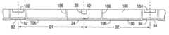
- Aligning the lapping guides along a common line perpendicular to the planes of the layersallows for easy diagnostic alignment measurement.
- the common linescould be positioned at distances D 1 and D 2 from the center of the recording head.
- the relative positions of the lapping guidesprovide offset information. For example, if the center of the near field transducer lapping guide is 20 nm to the left of the center of the SIM lapping guide, that probably means that there is an offset problem in the fabrication process.
- FIG. 10is a plan view of an air bearing surface 36 formed by lapping the layers of FIGS. 7-9 up to the plane 88 .
- the cross-sectional views of the triangular lapping guides 82 , 84 , 92 , 94 , 102 and 104 at the lapping planeare shown to have rectangular shapes.
- the SIM etchis done last, and then a thin layer of Au, Ag, or other metal is deposited creating the substantially vertical line 106 . Ideally the lines would be exactly perpendicular to the planes of the layers. This metal is the SIM sidewall that reflects the light in the SIM.
- FIG. 11is an enlarged view of one set of lapping guides of the structure of FIG. 10 .
- lapping guides 84 , 94 and 104would be centered on line 110 , which is oriented perpendicular to the planes of the layers. Since the lapping guides are positioned at a known, tightly controlled distance from the features of interest in the layers, the alignment of the lapping guides corresponds to alignment of the features of interest.
- Imaging analysis of the lapping guidescan be used to measure cross-track alignment of features in different layers and to measure the cross-track offset of such features with respect to each other.
- NFTwhich can be, for example, 50 nm wide
- SIMsolid immersion mirror
- the offset of each layer with respect to the ABScan be measured, and the cross-track offset of NFT to the center of the SIM can be measured.
- Imaging analysis of the offsetcan be implemented using a Critical Dimension Scanning Electron Microscope (CDSEM) and automated image analysis. Scanning of the beam across the exposed air bearing surface and subsequent collection of the reflected electrons enables measurement of the feature size.
- CDSEMCritical Dimension Scanning Electron Microscope
- Scanning of the beam across the exposed air bearing surface and subsequent collection of the reflected electronsenables measurement of the feature size.
- the SIM Width1, SIM Width2, NFT Width1, NFT Width2 and the offsetare measured.
- a commercial CDSEMsuch as from KLA-Tencor or FEI, can be used to image the set of lapping guides at a sufficiently high resolution, resulting in (for example) a 2 micron field of view with 4.16 nm pixels for each set of lapping guides.
- Commercially available automated image analysis softwaresuch as from National Instruments or from FEI can be used to measure the width of each lapping guide, and offsets between the lapping guides with respect to each other in a direction parallel to the planes of the layers (i.e., in the cross-track direction).
- NFT Width1NFT Width2
- SIM Width1SIM Width 2
- the lapping guidesare designed to be triangles where the height into the ABS is half the width of the base, the misalignment in a direction perpendicular to the ABS of the NFT is (NFT Width1 ⁇ NFT Width2)/4 and misalignment of the SIM is (SIM Width1 ⁇ SIM Width2)/4.
- the cross-track misalignment of the features of interestis equal to the measured offset of the corresponding lapping guides.
- the inventionprovides a method including the steps of fabricating a wafer having a plurality of layers, each including a feature of interest and a lapping guide structure positioned at a known location relative to the feature of interest, wherein the feature of interest and the lapping guide structure cross a common plane, and the features of interest in the plurality of layers are substantially aligned on a common line, lapping the wafer to the common plane to expose portions of the lapping guides, and measuring an offset of the lapping guides with respect to each other.
- the features of interestare the truncated end of the SIM core layer, the near field transducer, and the end of the write pole.
Landscapes
- Engineering & Computer Science (AREA)
- Manufacturing & Machinery (AREA)
- Physics & Mathematics (AREA)
- Electromagnetism (AREA)
- Magnetic Heads (AREA)
Abstract
Description
Claims (10)
Priority Applications (1)
| Application Number | Priority Date | Filing Date | Title |
|---|---|---|---|
| US12/370,976US7996986B2 (en) | 2009-02-13 | 2009-02-13 | Apparatus for forming magnetic recording heads |
Applications Claiming Priority (1)
| Application Number | Priority Date | Filing Date | Title |
|---|---|---|---|
| US12/370,976US7996986B2 (en) | 2009-02-13 | 2009-02-13 | Apparatus for forming magnetic recording heads |
Publications (2)
| Publication Number | Publication Date |
|---|---|
| US20100208391A1 US20100208391A1 (en) | 2010-08-19 |
| US7996986B2true US7996986B2 (en) | 2011-08-16 |
Family
ID=42559712
Family Applications (1)
| Application Number | Title | Priority Date | Filing Date |
|---|---|---|---|
| US12/370,976Expired - Fee RelatedUS7996986B2 (en) | 2009-02-13 | 2009-02-13 | Apparatus for forming magnetic recording heads |
Country Status (1)
| Country | Link |
|---|---|
| US (1) | US7996986B2 (en) |
Cited By (10)
| Publication number | Priority date | Publication date | Assignee | Title |
|---|---|---|---|---|
| US20110294398A1 (en)* | 2010-05-28 | 2011-12-01 | Western Digital (Fremont), Llc | Method and system for providing an electronic lapping guide corresponding to a near-field transducer of an energy assisted magnetic recording transducer |
| US8343364B1 (en) | 2010-06-08 | 2013-01-01 | Western Digital (Fremont), Llc | Double hard-mask mill back method of fabricating a near field transducer for energy assisted magnetic recording |
| US8526275B1 (en)* | 2012-04-27 | 2013-09-03 | Westerni Digital (Fremont), LLC | Systems and methods for dissipating heat from a near-field transducer in an energy assisted magnetic recording assembly |
| US8619512B1 (en) | 2012-06-22 | 2013-12-31 | Western Digital (Fremont), Llc | Stress buffer for near-field transducer in energy assisted magnetic recording and methods for fabricating the same |
| US8749790B1 (en) | 2011-12-08 | 2014-06-10 | Western Digital (Fremont), Llc | Structure and method to measure waveguide power absorption by surface plasmon element |
| US20140254339A1 (en)* | 2013-03-11 | 2014-09-11 | Seagate Technology Llc | Etch stop configuration |
| US8958271B1 (en) | 2013-09-03 | 2015-02-17 | Seagate Technology Llc | Peg height of near-field transducers |
| US9283651B2 (en) | 2013-09-06 | 2016-03-15 | Seagate Technology Llc | Apparatus including electrical lapping guide and methods of using the same |
| US9441938B1 (en) | 2013-10-08 | 2016-09-13 | Western Digital (Fremont), Llc | Test structures for measuring near field transducer disc length |
| US9881638B1 (en)* | 2014-12-17 | 2018-01-30 | Western Digital (Fremont), Llc | Method for providing a near-field transducer (NFT) for a heat assisted magnetic recording (HAMR) device |
Families Citing this family (20)
| Publication number | Priority date | Publication date | Assignee | Title |
|---|---|---|---|---|
| US8289650B2 (en)* | 2007-09-19 | 2012-10-16 | Seagate Technology Llc | HAMR recording head having a sloped wall pole |
| US8151441B1 (en) | 2008-03-27 | 2012-04-10 | Western Digital (Fremont), Llc | Method for providing and utilizing an electronic lapping guide in a magnetic recording transducer |
| US8165709B1 (en)* | 2009-02-26 | 2012-04-24 | Western Digital (Fremont), Llc | Four pad self-calibrating electronic lapping guide |
| US8291743B1 (en) | 2009-05-27 | 2012-10-23 | Western Digital (Fremont), Llc | Method and system for calibrating an electronic lapping guide for a beveled pole in a magnetic recording transducer |
| US8443510B1 (en) | 2009-05-28 | 2013-05-21 | Western Digital (Fremont), Llc | Method for utilizing an electronic lapping guide for a beveled pole in a magnetic recording transducer |
| US8307539B1 (en) | 2009-09-30 | 2012-11-13 | Western Digital (Fremont), Llc | Method for modeling devices in a wafer |
| US8385158B1 (en)* | 2009-10-06 | 2013-02-26 | Western Digital (Fremont), Llc | Method and system for providing a magnetic recording transducer having a planarized near-field transducer and a sloped pole |
| US8593914B2 (en) | 2010-12-22 | 2013-11-26 | Western Digital (Fremont), Llc | Method and system for optically coupling a laser with a transducer in an energy assisted magnetic recording disk drive |
| US8897103B2 (en) | 2011-09-27 | 2014-11-25 | Western Digital Technologies, Inc. | Disk drive calibrating a laser write power for heat assisted magnetic recording |
| US8861124B1 (en) | 2013-03-14 | 2014-10-14 | Western Digital (Fremont), Llc | Integrated sensor for monitoring laser power in a heat assisted magnetic recording disk drive |
| US8897102B1 (en) | 2013-04-02 | 2014-11-25 | Western Digital (Fremont), Llc | Method and system for measuring light delivery offsets in a heat assisted magnetic recording head |
| US9001628B1 (en) | 2013-12-16 | 2015-04-07 | Western Digital (Fremont), Llc | Assistant waveguides for evaluating main waveguide coupling efficiency and diode laser alignment tolerances for hard disk |
| US10290314B1 (en) | 2017-06-30 | 2019-05-14 | Seagate Technology Llc | Locating electrical contact pads on a slider body, and related row bars that include such slider bodies |
| US10672423B2 (en) | 2018-04-10 | 2020-06-02 | Seagate Technology Llc | Electronic test structures for one or more magnetoresistive elements, and related methods |
| US11389924B2 (en) | 2018-06-18 | 2022-07-19 | Seagate Technology Llc | Methods of lapping while heating one or more features, and related sliders, row bars, and systems |
| US11305397B2 (en) | 2018-06-18 | 2022-04-19 | Seagate Technology Llc | Lapping system that includes a lapping plate temperature control system, and related methods |
| US10468058B1 (en)* | 2018-06-28 | 2019-11-05 | Western Digital Technologies, Inc. | Magnetic write head with a tapered return pole |
| US10714128B2 (en) | 2018-10-11 | 2020-07-14 | Western Digital Technologies, Inc. | Magnetic write head with dual return pole |
| US11331765B1 (en)* | 2019-04-12 | 2022-05-17 | Seagate Technology Llc | Methods of lapping a substrate while heating at least a portion of the substrate, and related substrates and systems |
| US11094339B1 (en) | 2020-04-13 | 2021-08-17 | Seagate Technology Llc | Methods of manufacturing one or more sliders that includes a second lapping process after patterning, and related sliders |
Citations (11)
| Publication number | Priority date | Publication date | Assignee | Title |
|---|---|---|---|---|
| US4841625A (en) | 1982-05-07 | 1989-06-27 | Computer And Communications Technology Corporation | Automatic throat height control for film head |
| US5056353A (en)* | 1988-04-06 | 1991-10-15 | Sanyo Electric Co., Ltd. | Marker for detecting amount of working and process for producing thin film magnetic head |
| US5305559A (en)* | 1992-05-12 | 1994-04-26 | Ngk Insulators, Ltd. | Method of grinding core blank for magnetic heads, using markers for determining grinding depth for nominal magnetic gap depth |
| US5579717A (en) | 1994-10-13 | 1996-12-03 | International Business Machines Corporation | Method of grinding thin-film magnetic heads using optical grinding markers |
| US6003361A (en) | 1996-05-24 | 1999-12-21 | Seagate Technology, Inc. | System for predicting accurate MR sensor height |
| US6347983B1 (en) | 1999-06-09 | 2002-02-19 | Seagate Technology Llc | ELG for both MRE sensor height and resistance monitoring |
| US6884148B1 (en) | 2004-05-26 | 2005-04-26 | Headway Technologies, Inc. | Independently controlled read and write head stripe height parameters in slider back end process |
| US6935923B2 (en) | 2003-03-12 | 2005-08-30 | Seagate Technology Llc | Sensor stripe encapsulation layer in a read/write head |
| US20080141522A1 (en) | 2006-12-15 | 2008-06-19 | Hitachi Global Storage Technologies | Optical lapping guide for use in the manufacture of perpendicular magnetic write heads |
| US7610673B2 (en)* | 2004-04-05 | 2009-11-03 | Tdk Corporation | Method of manufacturing a vertical recording magnetic head |
| US7861400B2 (en)* | 2007-05-04 | 2011-01-04 | Hitachi Global Storage Technologies Netherlands, B.V. | Fabricating a write head with multiple electronic lapping guides |
- 2009
- 2009-02-13USUS12/370,976patent/US7996986B2/ennot_activeExpired - Fee Related
Patent Citations (11)
| Publication number | Priority date | Publication date | Assignee | Title |
|---|---|---|---|---|
| US4841625A (en) | 1982-05-07 | 1989-06-27 | Computer And Communications Technology Corporation | Automatic throat height control for film head |
| US5056353A (en)* | 1988-04-06 | 1991-10-15 | Sanyo Electric Co., Ltd. | Marker for detecting amount of working and process for producing thin film magnetic head |
| US5305559A (en)* | 1992-05-12 | 1994-04-26 | Ngk Insulators, Ltd. | Method of grinding core blank for magnetic heads, using markers for determining grinding depth for nominal magnetic gap depth |
| US5579717A (en) | 1994-10-13 | 1996-12-03 | International Business Machines Corporation | Method of grinding thin-film magnetic heads using optical grinding markers |
| US6003361A (en) | 1996-05-24 | 1999-12-21 | Seagate Technology, Inc. | System for predicting accurate MR sensor height |
| US6347983B1 (en) | 1999-06-09 | 2002-02-19 | Seagate Technology Llc | ELG for both MRE sensor height and resistance monitoring |
| US6935923B2 (en) | 2003-03-12 | 2005-08-30 | Seagate Technology Llc | Sensor stripe encapsulation layer in a read/write head |
| US7610673B2 (en)* | 2004-04-05 | 2009-11-03 | Tdk Corporation | Method of manufacturing a vertical recording magnetic head |
| US6884148B1 (en) | 2004-05-26 | 2005-04-26 | Headway Technologies, Inc. | Independently controlled read and write head stripe height parameters in slider back end process |
| US20080141522A1 (en) | 2006-12-15 | 2008-06-19 | Hitachi Global Storage Technologies | Optical lapping guide for use in the manufacture of perpendicular magnetic write heads |
| US7861400B2 (en)* | 2007-05-04 | 2011-01-04 | Hitachi Global Storage Technologies Netherlands, B.V. | Fabricating a write head with multiple electronic lapping guides |
Cited By (16)
| Publication number | Priority date | Publication date | Assignee | Title |
|---|---|---|---|---|
| US8964333B1 (en) | 2010-05-28 | 2015-02-24 | Western Digital (Fremont), Llc | Energy assisted magnetic recording transducer having an electronic lapping guide corresponding to a near-field transducer |
| US8375565B2 (en)* | 2010-05-28 | 2013-02-19 | Western Digital (Fremont), Llc | Method for providing an electronic lapping guide corresponding to a near-field transducer of an energy assisted magnetic recording transducer |
| US20110294398A1 (en)* | 2010-05-28 | 2011-12-01 | Western Digital (Fremont), Llc | Method and system for providing an electronic lapping guide corresponding to a near-field transducer of an energy assisted magnetic recording transducer |
| US8343364B1 (en) | 2010-06-08 | 2013-01-01 | Western Digital (Fremont), Llc | Double hard-mask mill back method of fabricating a near field transducer for energy assisted magnetic recording |
| US8749790B1 (en) | 2011-12-08 | 2014-06-10 | Western Digital (Fremont), Llc | Structure and method to measure waveguide power absorption by surface plasmon element |
| US8526275B1 (en)* | 2012-04-27 | 2013-09-03 | Westerni Digital (Fremont), LLC | Systems and methods for dissipating heat from a near-field transducer in an energy assisted magnetic recording assembly |
| US8619512B1 (en) | 2012-06-22 | 2013-12-31 | Western Digital (Fremont), Llc | Stress buffer for near-field transducer in energy assisted magnetic recording and methods for fabricating the same |
| US20140254339A1 (en)* | 2013-03-11 | 2014-09-11 | Seagate Technology Llc | Etch stop configuration |
| US9142231B2 (en)* | 2013-03-11 | 2015-09-22 | Seagate Technology Llc | Method of making a transducer head |
| US9437221B2 (en) | 2013-03-11 | 2016-09-06 | Seagate Technology Llc | Method of making a transducer head |
| US8958271B1 (en) | 2013-09-03 | 2015-02-17 | Seagate Technology Llc | Peg height of near-field transducers |
| US9396748B2 (en) | 2013-09-03 | 2016-07-19 | Seagate Technology Llc | Peg height of near-field transducers |
| US9283651B2 (en) | 2013-09-06 | 2016-03-15 | Seagate Technology Llc | Apparatus including electrical lapping guide and methods of using the same |
| US9441938B1 (en) | 2013-10-08 | 2016-09-13 | Western Digital (Fremont), Llc | Test structures for measuring near field transducer disc length |
| US9881638B1 (en)* | 2014-12-17 | 2018-01-30 | Western Digital (Fremont), Llc | Method for providing a near-field transducer (NFT) for a heat assisted magnetic recording (HAMR) device |
| US10553241B2 (en) | 2014-12-17 | 2020-02-04 | Western Digital Technologies, Inc. | Near-field transducer (NFT) for a heat assisted magnetic recording (HAMR) device |
Also Published As
| Publication number | Publication date |
|---|---|
| US20100208391A1 (en) | 2010-08-19 |
Similar Documents
| Publication | Publication Date | Title |
|---|---|---|
| US7996986B2 (en) | Apparatus for forming magnetic recording heads | |
| US8964333B1 (en) | Energy assisted magnetic recording transducer having an electronic lapping guide corresponding to a near-field transducer | |
| US8307540B1 (en) | Method for providing an energy assisted magnetic recording (EAMR) transducer | |
| JP4138777B2 (en) | Lapping guide system and magnetic recording / reproducing head array polishing method | |
| US7133253B1 (en) | Pole tip with sides flared at media-facing surface | |
| US8797686B1 (en) | Magnetic recording transducer with short effective throat height and method of fabrication | |
| US8065786B2 (en) | Manufacturing method of heat-assisted magnetic head constituted of slider and light source unit | |
| US8009386B2 (en) | Magnetic tape head with magnetic head layer formed on base substrate | |
| US8649245B2 (en) | Direct waveguide light delivery to NFT for heat assisted magnetic recording | |
| US7142391B2 (en) | Thin film head, producing method thereof and magnetic disk apparatus | |
| US8065787B2 (en) | Method of manufacturing a thermally assisted magnetic head | |
| US7603762B2 (en) | Optical lapping guide for use in the manufacture of perpendicular magnetic write heads | |
| US8493821B1 (en) | Thermally-assisted magnetic recording head including a shield | |
| US9142231B2 (en) | Method of making a transducer head | |
| JP2005317188A (en) | Flat type perpendicular recording head | |
| US8691102B1 (en) | Method of manufacturing plasmon generator | |
| US8454848B2 (en) | Method of manufacturing plasmon generator | |
| US7454828B2 (en) | Method for manufacturing a magnetic write head | |
| US8400884B1 (en) | Method of manufacturing plasmon generator | |
| US6744582B2 (en) | Thermal-assisted magnetic storage device and method for driving the reading/writing head thereof | |
| US8614863B2 (en) | Row bar with smart sensor for forming sliders and method of manufacturing slider | |
| US10290314B1 (en) | Locating electrical contact pads on a slider body, and related row bars that include such slider bodies | |
| US8472287B1 (en) | Thermally-assisted magnetic recording head having a groove for inserting into suspension | |
| JP2996562B2 (en) | Method for manufacturing thin-film magnetic head | |
| JP3410045B2 (en) | Method for manufacturing thin-film magnetic head |
Legal Events
| Date | Code | Title | Description |
|---|---|---|---|
| AS | Assignment | Owner name:SEAGATE TECHNOLOGY LLC, CALIFORNIA Free format text:ASSIGNMENT OF ASSIGNORS INTEREST;ASSIGNOR:GOKEMEIJER, NILS JAN;REEL/FRAME:022256/0155 Effective date:20090211 | |
| AS | Assignment | Owner name:WELLS FARGO BANK, NATIONAL ASSOCIATION, AS COLLATERAL AGENT AND SECOND PRIORITY REPRESENTATIVE, CALIFORNIA Free format text:SECURITY AGREEMENT;ASSIGNORS:MAXTOR CORPORATION;SEAGATE TECHNOLOGY LLC;SEAGATE TECHNOLOGY INTERNATIONAL;REEL/FRAME:022757/0017 Effective date:20090507 Owner name:JPMORGAN CHASE BANK, N.A., AS ADMINISTRATIVE AGENT AND FIRST PRIORITY REPRESENTATIVE, NEW YORK Free format text:SECURITY AGREEMENT;ASSIGNORS:MAXTOR CORPORATION;SEAGATE TECHNOLOGY LLC;SEAGATE TECHNOLOGY INTERNATIONAL;REEL/FRAME:022757/0017 Effective date:20090507 Owner name:JPMORGAN CHASE BANK, N.A., AS ADMINISTRATIVE AGENT Free format text:SECURITY AGREEMENT;ASSIGNORS:MAXTOR CORPORATION;SEAGATE TECHNOLOGY LLC;SEAGATE TECHNOLOGY INTERNATIONAL;REEL/FRAME:022757/0017 Effective date:20090507 Owner name:WELLS FARGO BANK, NATIONAL ASSOCIATION, AS COLLATE Free format text:SECURITY AGREEMENT;ASSIGNORS:MAXTOR CORPORATION;SEAGATE TECHNOLOGY LLC;SEAGATE TECHNOLOGY INTERNATIONAL;REEL/FRAME:022757/0017 Effective date:20090507 | |
| AS | Assignment | Owner name:SEAGATE TECHNOLOGY LLC, CALIFORNIA Free format text:RELEASE;ASSIGNOR:JPMORGAN CHASE BANK, N.A., AS ADMINISTRATIVE AGENT;REEL/FRAME:025662/0001 Effective date:20110114 Owner name:MAXTOR CORPORATION, CALIFORNIA Free format text:RELEASE;ASSIGNOR:JPMORGAN CHASE BANK, N.A., AS ADMINISTRATIVE AGENT;REEL/FRAME:025662/0001 Effective date:20110114 Owner name:SEAGATE TECHNOLOGY HDD HOLDINGS, CALIFORNIA Free format text:RELEASE;ASSIGNOR:JPMORGAN CHASE BANK, N.A., AS ADMINISTRATIVE AGENT;REEL/FRAME:025662/0001 Effective date:20110114 Owner name:SEAGATE TECHNOLOGY INTERNATIONAL, CALIFORNIA Free format text:RELEASE;ASSIGNOR:JPMORGAN CHASE BANK, N.A., AS ADMINISTRATIVE AGENT;REEL/FRAME:025662/0001 Effective date:20110114 | |
| AS | Assignment | Owner name:THE BANK OF NOVA SCOTIA, AS ADMINISTRATIVE AGENT, CANADA Free format text:SECURITY AGREEMENT;ASSIGNOR:SEAGATE TECHNOLOGY LLC;REEL/FRAME:026010/0350 Effective date:20110118 Owner name:THE BANK OF NOVA SCOTIA, AS ADMINISTRATIVE AGENT, Free format text:SECURITY AGREEMENT;ASSIGNOR:SEAGATE TECHNOLOGY LLC;REEL/FRAME:026010/0350 Effective date:20110118 | |
| ZAAA | Notice of allowance and fees due | Free format text:ORIGINAL CODE: NOA | |
| ZAAB | Notice of allowance mailed | Free format text:ORIGINAL CODE: MN/=. | |
| STCF | Information on status: patent grant | Free format text:PATENTED CASE | |
| AS | Assignment | Owner name:SEAGATE TECHNOLOGY LLC, CALIFORNIA Free format text:TERMINATION AND RELEASE OF SECURITY INTEREST IN PATENT RIGHTS;ASSIGNOR:WELLS FARGO BANK, NATIONAL ASSOCIATION, AS COLLATERAL AGENT AND SECOND PRIORITY REPRESENTATIVE;REEL/FRAME:030833/0001 Effective date:20130312 Owner name:EVAULT INC. (F/K/A I365 INC.), CALIFORNIA Free format text:TERMINATION AND RELEASE OF SECURITY INTEREST IN PATENT RIGHTS;ASSIGNOR:WELLS FARGO BANK, NATIONAL ASSOCIATION, AS COLLATERAL AGENT AND SECOND PRIORITY REPRESENTATIVE;REEL/FRAME:030833/0001 Effective date:20130312 Owner name:SEAGATE TECHNOLOGY INTERNATIONAL, CAYMAN ISLANDS Free format text:TERMINATION AND RELEASE OF SECURITY INTEREST IN PATENT RIGHTS;ASSIGNOR:WELLS FARGO BANK, NATIONAL ASSOCIATION, AS COLLATERAL AGENT AND SECOND PRIORITY REPRESENTATIVE;REEL/FRAME:030833/0001 Effective date:20130312 Owner name:SEAGATE TECHNOLOGY US HOLDINGS, INC., CALIFORNIA Free format text:TERMINATION AND RELEASE OF SECURITY INTEREST IN PATENT RIGHTS;ASSIGNOR:WELLS FARGO BANK, NATIONAL ASSOCIATION, AS COLLATERAL AGENT AND SECOND PRIORITY REPRESENTATIVE;REEL/FRAME:030833/0001 Effective date:20130312 | |
| FPAY | Fee payment | Year of fee payment:4 | |
| MAFP | Maintenance fee payment | Free format text:PAYMENT OF MAINTENANCE FEE, 8TH YEAR, LARGE ENTITY (ORIGINAL EVENT CODE: M1552); ENTITY STATUS OF PATENT OWNER: LARGE ENTITY Year of fee payment:8 | |
| FEPP | Fee payment procedure | Free format text:MAINTENANCE FEE REMINDER MAILED (ORIGINAL EVENT CODE: REM.); ENTITY STATUS OF PATENT OWNER: LARGE ENTITY | |
| LAPS | Lapse for failure to pay maintenance fees | Free format text:PATENT EXPIRED FOR FAILURE TO PAY MAINTENANCE FEES (ORIGINAL EVENT CODE: EXP.); ENTITY STATUS OF PATENT OWNER: LARGE ENTITY | |
| STCH | Information on status: patent discontinuation | Free format text:PATENT EXPIRED DUE TO NONPAYMENT OF MAINTENANCE FEES UNDER 37 CFR 1.362 | |
| FP | Lapsed due to failure to pay maintenance fee | Effective date:20230816 | |
| AS | Assignment | Owner name:SEAGATE TECHNOLOGY PUBLIC LIMITED COMPANY, CALIFORNIA Free format text:RELEASE BY SECURED PARTY;ASSIGNOR:THE BANK OF NOVA SCOTIA;REEL/FRAME:072193/0001 Effective date:20250303 Owner name:SEAGATE TECHNOLOGY, CALIFORNIA Free format text:RELEASE BY SECURED PARTY;ASSIGNOR:THE BANK OF NOVA SCOTIA;REEL/FRAME:072193/0001 Effective date:20250303 Owner name:SEAGATE TECHNOLOGY HDD HOLDINGS, CALIFORNIA Free format text:RELEASE BY SECURED PARTY;ASSIGNOR:THE BANK OF NOVA SCOTIA;REEL/FRAME:072193/0001 Effective date:20250303 Owner name:I365 INC., CALIFORNIA Free format text:RELEASE BY SECURED PARTY;ASSIGNOR:THE BANK OF NOVA SCOTIA;REEL/FRAME:072193/0001 Effective date:20250303 Owner name:SEAGATE TECHNOLOGY LLC, CALIFORNIA Free format text:RELEASE BY SECURED PARTY;ASSIGNOR:THE BANK OF NOVA SCOTIA;REEL/FRAME:072193/0001 Effective date:20250303 Owner name:SEAGATE TECHNOLOGY INTERNATIONAL, CAYMAN ISLANDS Free format text:RELEASE BY SECURED PARTY;ASSIGNOR:THE BANK OF NOVA SCOTIA;REEL/FRAME:072193/0001 Effective date:20250303 Owner name:SEAGATE HDD CAYMAN, CAYMAN ISLANDS Free format text:RELEASE BY SECURED PARTY;ASSIGNOR:THE BANK OF NOVA SCOTIA;REEL/FRAME:072193/0001 Effective date:20250303 Owner name:SEAGATE TECHNOLOGY (US) HOLDINGS, INC., CALIFORNIA Free format text:RELEASE BY SECURED PARTY;ASSIGNOR:THE BANK OF NOVA SCOTIA;REEL/FRAME:072193/0001 Effective date:20250303 |