US7994996B2 - Multi-beam antenna - Google Patents
Multi-beam antennaDownload PDFInfo
- Publication number
- US7994996B2 US7994996B2US11/627,369US62736907AUS7994996B2US 7994996 B2US7994996 B2US 7994996B2US 62736907 AUS62736907 AUS 62736907AUS 7994996 B2US7994996 B2US 7994996B2
- Authority
- US
- United States
- Prior art keywords
- antenna
- dielectric substrate
- fire
- elements
- lens
- Prior art date
- Legal status (The legal status is an assumption and is not a legal conclusion. Google has not performed a legal analysis and makes no representation as to the accuracy of the status listed.)
- Expired - Fee Related, expires
Links
Images

Classifications
- H—ELECTRICITY
- H01—ELECTRIC ELEMENTS
- H01Q—ANTENNAS, i.e. RADIO AERIALS
- H01Q13/00—Waveguide horns or mouths; Slot antennas; Leaky-waveguide antennas; Equivalent structures causing radiation along the transmission path of a guided wave
- H01Q13/08—Radiating ends of two-conductor microwave transmission lines, e.g. of coaxial lines, of microstrip lines
- H01Q13/085—Slot-line radiating ends
- H—ELECTRICITY
- H01—ELECTRIC ELEMENTS
- H01Q—ANTENNAS, i.e. RADIO AERIALS
- H01Q1/00—Details of, or arrangements associated with, antennas
- H01Q1/27—Adaptation for use in or on movable bodies
- H01Q1/32—Adaptation for use in or on road or rail vehicles
- H01Q1/3208—Adaptation for use in or on road or rail vehicles characterised by the application wherein the antenna is used
- H01Q1/3233—Adaptation for use in or on road or rail vehicles characterised by the application wherein the antenna is used particular used as part of a sensor or in a security system, e.g. for automotive radar, navigation systems
- H—ELECTRICITY
- H01—ELECTRIC ELEMENTS
- H01Q—ANTENNAS, i.e. RADIO AERIALS
- H01Q1/00—Details of, or arrangements associated with, antennas
- H01Q1/48—Earthing means; Earth screens; Counterpoises
- H—ELECTRICITY
- H01—ELECTRIC ELEMENTS
- H01Q—ANTENNAS, i.e. RADIO AERIALS
- H01Q19/00—Combinations of primary active antenna elements and units with secondary devices, e.g. with quasi-optical devices, for giving the antenna a desired directional characteristic
- H01Q19/06—Combinations of primary active antenna elements and units with secondary devices, e.g. with quasi-optical devices, for giving the antenna a desired directional characteristic using refracting or diffracting devices, e.g. lens
- H01Q19/062—Combinations of primary active antenna elements and units with secondary devices, e.g. with quasi-optical devices, for giving the antenna a desired directional characteristic using refracting or diffracting devices, e.g. lens for focusing
- H—ELECTRICITY
- H01—ELECTRIC ELEMENTS
- H01Q—ANTENNAS, i.e. RADIO AERIALS
- H01Q19/00—Combinations of primary active antenna elements and units with secondary devices, e.g. with quasi-optical devices, for giving the antenna a desired directional characteristic
- H01Q19/28—Combinations of primary active antenna elements and units with secondary devices, e.g. with quasi-optical devices, for giving the antenna a desired directional characteristic using a secondary device in the form of two or more substantially straight conductive elements
- H01Q19/30—Combinations of primary active antenna elements and units with secondary devices, e.g. with quasi-optical devices, for giving the antenna a desired directional characteristic using a secondary device in the form of two or more substantially straight conductive elements the primary active element being centre-fed and substantially straight, e.g. Yagi antenna
- H—ELECTRICITY
- H01—ELECTRIC ELEMENTS
- H01Q—ANTENNAS, i.e. RADIO AERIALS
- H01Q21/00—Antenna arrays or systems
- H01Q21/29—Combinations of different interacting antenna units for giving a desired directional characteristic
- H—ELECTRICITY
- H01—ELECTRIC ELEMENTS
- H01Q—ANTENNAS, i.e. RADIO AERIALS
- H01Q25/00—Antennas or antenna systems providing at least two radiating patterns
- H—ELECTRICITY
- H01—ELECTRIC ELEMENTS
- H01Q—ANTENNAS, i.e. RADIO AERIALS
- H01Q3/00—Arrangements for changing or varying the orientation or the shape of the directional pattern of the waves radiated from an antenna or antenna system
- H01Q3/24—Arrangements for changing or varying the orientation or the shape of the directional pattern of the waves radiated from an antenna or antenna system varying the orientation by switching energy from one active radiating element to another, e.g. for beam switching
- H01Q3/245—Arrangements for changing or varying the orientation or the shape of the directional pattern of the waves radiated from an antenna or antenna system varying the orientation by switching energy from one active radiating element to another, e.g. for beam switching in the focal plane of a focussing device
Definitions
- FIG. 1illustrates a top view of a first embodiment of a multi-beam antenna comprising an electromagnetic lens
- FIG. 2illustrates a fragmentary side cross-sectional view of the embodiment illustrated in FIG. 1 ;
- FIG. 3illustrates a fragmentary side cross-sectional view of the embodiment illustrated in FIG. 1 , incorporating a truncated electromagnetic lens;
- FIG. 4illustrates a fragmentary side cross-sectional view of an embodiment illustrating various locations of a dielectric substrate, relative to an electromagnetic lens
- FIG. 5illustrates an embodiment of a multi-beam antenna, wherein each antenna feed element is operatively coupled to a separate signal
- FIG. 6illustrates an embodiment of a multi-beam antenna, wherein the associated switching network is located separately from the dielectric substrate;
- FIG. 7illustrates a top view of a second embodiment of a multi-beam antenna comprising a plurality of electromagnetic lenses located proximate to one edge of a dielectric substrate;
- FIG. 8illustrates a top view of a third embodiment of a multi-beam antenna comprising a plurality of electromagnetic lenses located proximate to opposite edges of a dielectric substrate;
- FIG. 9illustrates a side view of the third embodiment illustrated in FIG. 8 , further comprising a plurality of reflectors;
- FIG. 10illustrates a fourth embodiment of a multi-beam antenna, comprising an electromagnetic lens and a reflector
- FIG. 11illustrates a fifth embodiment of a multi-beam antenna
- FIG. 12illustrates a top view of a sixth embodiment of a multi-beam antenna comprising a discrete lens array
- FIG. 13illustrates a fragmentary side cross-sectional view of the embodiment illustrated in FIG. 12 ;
- FIG. 14illustrates a block diagram of a lens element of a discrete lens array
- FIG. 15 aillustrates a first side of one embodiment of a planar discrete lens array
- FIG. 15 billustrates a second side of the embodiment of the planar discrete lens array illustrated in FIG. 15 a;
- FIG. 16illustrates a plot of delay as a function of radial location on the planar discrete lens array illustrated in FIGS. 15 a and 15 b;
- FIG. 17illustrates a fragmentary cross sectional isometric view of a first embodiment of a discrete lens antenna element
- FIG. 18illustrates an isometric view of the first embodiment of a discrete lens antenna element illustrated in FIG. 17 , isolated from associated dielectric substrates;
- FIG. 19illustrates an isometric view of a second embodiment of a discrete lens antenna element
- FIG. 20illustrates an isometric view of a third embodiment of a discrete lens antenna element, isolated from associated dielectric substrates;
- FIG. 21illustrates a cross sectional view of the third embodiment of the discrete lens antenna element
- FIG. 22illustrates a plan view of a second embodiment of a discrete lens array
- FIG. 23illustrates an isometric view of a fourth embodiment of a discrete lens antenna element, isolated from associated dielectric substrates;
- FIG. 24 aillustrates a cross sectional view of the fourth embodiment of the discrete lens antenna element of a third embodiment of a discrete lens array
- FIG. 24 billustrates a cross sectional view of the fourth embodiment of a discrete lens antenna element of a fourth embodiment of a discrete lens array
- FIG. 25illustrates a fragmentary cross sectional isometric view of a fifth embodiment of a discrete lens antenna element of a reflective discrete lens array
- FIG. 26illustrates a seventh embodiment of a multi-beam antenna, comprising a discrete lens array and a reflector
- FIG. 27illustrates an eighth embodiment of a multi-beam antenna.
- FIG. 28illustrates a top plan view of a first embodiment of a fifth aspect of a multi-beam antenna
- FIG. 29illustrates a side cross-sectional view of the embodiment of FIG. 28 ;
- FIG. 30illustrates a top plan view of an embodiment of the fifth aspect of the multi-beam antenna
- FIGS. 31 a - 31 fillustrate various embodiments of tapered slot antenna elements
- FIG. 32illustrates a tapered slot antenna element and an associated coordinate system
- FIG. 33illustrates a junction where a microstrip line is adapted to couple to a slotline feeding a tapered slot antenna
- FIG. 34illustrates a bottom view of the embodiment of the multi-beam antenna illustrated in FIG. 30 interfaced to an associated switch network;
- FIG. 35illustrates a bottom view of the embodiment of the multi-beam antenna illustrated in FIG. 30 with associated receiver circuitry
- FIG. 36illustrates a detailed view of the receiver circuitry for the embodiment illustrated in FIG. 35 ;
- FIG. 37illustrates an antenna gain pattern for the multi-beam antenna illustrated in FIGS. 30 and 35 ;
- FIG. 38 aillustrates an isometric view of an embodiment of a sixth aspect of a multi-beam antenna incorporating a bi-conical reflector
- FIG. 38 billustrates a cross-sectional view of the embodiment of the multi-beam antenna illustrated in FIG. 38 a incorporating a bi-conical reflector
- FIG. 39 aillustrates a top plan view of an embodiment of a seventh aspect of a multi-beam antenna incorporating a conformal cylindrical dielectric lens
- FIG. 39 billustrates a cross-sectional view of the embodiment of the multi-beam antenna illustrated in FIG. 39 a incorporating a circular cylindrical lens;
- FIG. 40 aillustrates a top plan view of an embodiment of an eighth aspect of a multi-beam antenna incorporating a discrete lens array
- FIG. 40 billustrates a cross-sectional view of the embodiment of the multi-beam antenna illustrated in FIG. 40 a incorporating a discrete lens array
- FIG. 41illustrates a first side of a planar discrete lens array
- FIG. 42illustrates a plot of delay as a function of transverse location on the planar discrete lens array of FIG. 41 ;
- FIG. 43 aillustrates a top plan view of an embodiment of a ninth aspect of a multi-beam antenna incorporating a dipole antenna adapted to cooperate with an associated corner reflector;
- FIG. 43 billustrates a cross-sectional view of the embodiment of the multi-beam antenna illustrated in FIG. 43 a incorporating a dipole antenna and an associated corner reflector;
- FIGS. 44 a and 44 billustrate a Yagi-Uda antenna element with a first embodiment of an associated feed circuit
- FIG. 45illustrates the operation of the Yagi-Uda antenna element illustrated in FIGS. 44 a and 44 b in cooperation with a dielectric lens having a circular profile;
- FIG. 46illustrates a Yagi-Uda antenna element with a second embodiment of an associated feed circuit
- FIG. 47illustrates an embodiment of a tenth aspect of a multi-beam antenna incorporating a plurality of Yagi-Uda antenna elements on a concave edge of a dielectric substrate;
- FIG. 48illustrates an embodiment of an eleventh aspect of a multi-beam antenna incorporating a plurality of Yagi-Uda antenna elements on a concave edge of a dielectric substrate, in cooperation with an at least partially spherical dielectric lens;
- FIGS. 49 a and 49 billustrate an embodiment of a twelfth aspect of a multi-beam antenna incorporating a plurality of endfire antenna elements on a concave edge of a dielectric substrate, in cooperation with an associated bi-conical reflector;
- FIG. 50illustrates a circular multi-beam antenna
- FIGS. 51 a and 51 billustrate a first non-planar embodiment of a thirteenth aspect of a multi-beam antenna
- FIGS. 52 a and 52 billustrate a second non-planar embodiment of the thirteenth aspect of a multi-beam antenna
- FIGS. 53 a and 53 billustrate an embodiment of a fourteenth aspect of a multi-beam antenna incorporating a plurality of monopole antennas with associated corner reflectors;
- FIGS. 54 a and 54 billustrate an embodiment of a fifteenth aspect of a multi-beam antenna incorporating a plurality of monopole antennas with associated corner reflectors;
- FIG. 55 aillustrates a plan view of a fifth embodiment discrete lens array
- FIG. 55 billustrates a side view of the fifth embodiment of the discrete lens array
- FIG. 55 cillustrates a side cross-sectional view of the fifth embodiment of the discrete lens array, illustrating a sixth embodiment of associated discrete lens antenna elements incorporated therein;
- FIG. 56illustrates an expanded fragmentary cross-sectional side view of a portion of the fifth embodiment of the discrete lens array, and the sixth embodiment of associated discrete lens antenna elements, illustrated in FIG. 55 c ;
- FIG. 57illustrates an expanded cross-sectional plan view of a portion of the sixth embodiment of associated discrete lens antenna element illustrated in FIG. 56 .
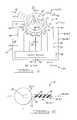
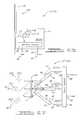
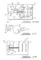
- a multi-beam antenna 10 , 10 . 1comprises at least one electromagnetic lens 12 and a plurality of antenna feed elements 14 on a dielectric substrate 16 proximate to a first edge 18 thereof, wherein the plurality of antenna feed elements 14 are adapted to radiate or receive a corresponding plurality of beams of electromagnetic energy 20 through the at least one electromagnetic lens 12 .
- the at least one electromagnetic lens 12has a first side 22 having a first contour 24 at an intersection of the first side 22 with a reference surface 26 , for example, a plane 26 . 1 .
- the at least one electromagnetic lens 12acts to diffract the electromagnetic wave from the respective antenna feed elements 14 , wherein different antenna feed elements 14 at different locations and in different directions relative to the at least one electromagnetic lens 12 generate different associated different beams of electromagnetic energy 20 .
- the at least one electromagnetic lens 12has a refractive index n different from free space, for example, a refractive index n greater than one (1).
- the at least one electromagnetic lens 12may be constructed of a material such as REXOLITETM, TEFLONTM, polyethylene, polystyrene or some other dielectric; or a plurality of different materials having different refractive indices, for example as in a Luneburg lens.
- the shape and size of the at least one electromagnetic lens 12 , the refractive index n thereof, and the relative position of the antenna feed elements 14 to the electromagnetic lens 12are adapted in accordance with the radiation patterns of the antenna feed elements 14 to provide a desired pattern of radiation of the respective beams of electromagnetic energy 20 exiting the second side 28 of the at least one electromagnetic lens 12 .
- the at least one electromagnetic lens 12is illustrated as a spherical lens 12 ′ in FIGS. 1 and 2
- the at least one electromagnetic lens 12is not limited to any one particular design, and may, for example, comprise either a spherical lens, a Luneburg lens, a spherical shell lens, a hemispherical lens, an at least partially spherical lens, an at least partially spherical shell lens, an elliptical lens, a cylindrical lens, or a rotational lens.
- one or more portions of the electromagnetic lens 12may be truncated for improved packaging, without significantly impacting the performance of the associated multi-beam antenna 10 , 10 . 1 .
- FIG. 3illustrates an at least partially spherical electromagnetic lens 12 ′′ with opposing first 27 and second 29 portions removed therefrom.
- the first edge 18 of the dielectric substrate 16comprises a second contour 30 that is proximate to the first contour 24 .
- the first edge 18 of the dielectric substrate 16is located on the reference surface 26 , and is positioned proximate to the first side 22 of one of the at least one electromagnetic lens 12 .
- the dielectric substrate 16is located relative to the electromagnetic lens 12 so as to provide for the diffraction by the at least one electromagnetic lens 12 necessary to form the beams of electromagnetic energy 20 .
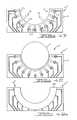
- a multi-beam antenna 10comprising a planar dielectric substrate 16 located on reference surface 26 comprising a plane 26 . 1 , in combination with an electromagnetic lens 12 having a center 32 , for example, a spherical lens 12 ′; the plane 26 .
- the dielectric substrate 16may also be displaced relative to the center 32 of the electromagnetic lens 12 , for example on one or the other side of the center 32 as illustrated by dielectric substrates 16 ′ and 16 ′′, which are located on respective reference surfaces 26 ′ and 26 ′′.
- the dielectric substrate 16is, for example, a material with low loss at an operating frequency, for example, DUROIDTM, a TEFLONTM containing material, a ceramic material, or a composite material such as an epoxy/fiberglass composite.
- the dielectric substrate 16comprises a dielectric 16 . 1 of a circuit board 34 , for example, a printed circuit board 34 . 1 comprising at least one conductive layer 36 adhered to the dielectric substrate 16 , from which the antenna feed elements 14 and other associated circuit traces 38 are formed, for example, by subtractive technology, for example, chemical or ion etching, or stamping; or additive techniques, for example, deposition, bonding or lamination.
- each antenna feed element 14comprises a least one conductor 40 operatively connected to the dielectric substrate 16 .
- at least one of the antenna feed elements 14comprises an end-fire antenna element 14 . 1 adapted to launch or receive electromagnetic waves in a direction 42 substantially towards or from the first side 22 of the at least one electromagnetic lens 12 , wherein different end-fire antenna elements 14 . 1 are located at different locations along the second contour 30 so as to launch or receive respective electromagnetic waves in different directions 42 .
- An end-fire antenna element 14is located on the dielectric substrate 16 along the second contour 30 of the first edge 18 , wherein each antenna feed element 14 comprises a least one conductor 40 operatively connected to the dielectric substrate 16 .
- at least one of the antenna feed elements 14comprises an end-fire antenna element 14 . 1 adapted to launch or receive electromagnetic waves in a direction 42 substantially towards or from the first side 22 of the at least one electromagnetic lens 12 , wherein different end-fire antenna elements 14 . 1 are located at different locations along the second contour 30 so as to launch or receive respective electromagnetic
- a Yagi-Uda antennamay, for example, comprise either a Yagi-Uda antenna, a coplanar horn antenna (also known as a tapered slot antenna), a Vivaldi antenna, a tapered dielectric rod, a slot antenna, a dipole antenna, or a helical antenna, each of which is capable of being formed on the dielectric substrate 16 , for example, from a printed circuit board 34 . 1 , for example, by subtractive technology, for example, chemical or ion etching, or stamping; or additive techniques, for example, deposition, bonding or lamination.
- the antenna feed elements 14may be used for transmitting, receiving or both transmitting and receiving.
- the direction 42 of the one or more beams of electromagnetic energy 20 , 20 ′, 20 ′′ through the electromagnetic lens 12 , 12 ′is responsive to the relative location of the dielectric substrate 16 , 16 ′ or 16 ′′ and the associated reference surface 26 , 26 ′ or 26 ′′ relative to the center 32 of the electromagnetic lens 12 .
- the directions 42 of the one or more beams of electromagnetic energy 20are nominally aligned with the reference surface 26 .
- the resulting one or more beams of electromagnetic energy 20 ′propagate in directions 42 ′ below the center 32 .
- the resulting one or more beams of electromagnetic energy 20 ′′propagate in directions 42 ′′ above the center 32 .
- the multi-beam antenna 10may further comprise at least one transmission line 44 on the dielectric substrate 16 operatively connected to a feed port 46 of one of the plurality of antenna feed elements 14 , for feeding a signal to the associated antenna feed element 14 .
- the at least one transmission line 44may comprise either a stripline, a microstrip line, an inverted microstrip line, a slotline, an image line, an insulated image line, a tapped image line, a coplanar stripline, or a coplanar waveguide line formed on the dielectric substrate 16 , for example, from a printed circuit board 34 . 1 , for example, by subtractive technology, for example, chemical or ion etching, or stamping; or additive techniques, for example, deposition, bonding or lamination.
- the multi-beam antenna 10may further comprise a switching network 48 having at least one input 50 and a plurality of outputs 52 , wherein the at least one input 50 is operatively connected—for example, via at least one above described transmission line 44 —to a corporate antenna feed port 54 , and each output 52 of the plurality of outputs 52 is connected—for example, via at least one above described transmission line 44 —to a respective feed port 46 of a different antenna feed element 14 of the plurality of antenna feed elements 14 .
- the switching network 48further comprises at least one control port 56 for controlling which outputs 52 are connected to the at least one input 50 at a given time.
- the switching network 48may, for example, comprise either a plurality of micro-mechanical switches, PIN diode switches, transistor switches, or a combination thereof, and may, for example, be operatively connected to the dielectric substrate 16 , for example, by surface mount to an associated conductive layer 36 of a printed circuit board 34 . 1 .
- a feed signal 58 applied to the corporate antenna feed port 54is either blocked—for example, by an open circuit, by reflection or by absorption,—or switched to the associated feed port 46 of one or more antenna feed elements 14 , via one or more associated transmission lines 44 , by the switching network 48 , responsive to a control signal 60 applied to the control port 56 .
- the feed signal 58may either comprise a single signal common to each antenna feed element 14 , or a plurality of signals associated with different antenna feed elements 14 .
- Each antenna feed element 14 to which the feed signal 58 is appliedlaunches an associated electromagnetic wave into the first side 22 of the associated electromagnetic lens 12 , which is diffracted thereby to form an associated beam of electromagnetic energy 20 .
- the associated beams of electromagnetic energy 20 launched by different antenna feed elements 14propagate in different associated directions 42 .
- the various beams of electromagnetic energy 20may be generated individually at different times so as to provide for a scanned beam of electromagnetic energy 20 . Alternately, two or more beams of electromagnetic energy 20 may be generated simultaneously.
- different antenna feed elements 14may be driven by different frequencies that, for example, are either directly switched to the respective antenna feed elements 14 , or switched via an associated switching network 48 having a plurality of inputs 50 , at least some of which are connected to different feed signals 58 .
- the multi-beam antenna 10 , 10 . 1may be adapted so that the respective signals are associated with the respective antenna feed elements 14 in a one-to-one relationship, thereby precluding the need for an associated switching network 48 .
- each antenna feed element 14can be operatively connected to an associated signal 59 through an associated processing element 61 .
- the respective antenna feed elements 14are used to receive electromagnetic energy, and the respective processing elements 61 comprise detectors.
- the respective antenna feed elements 14are used to both transmit and receive electromagnetic energy, and the respective processing elements 61 comprise transmit/receive modules or transceivers.
- the switching network 48if used, need not be collocated on a common dielectric substrate 16 , but can be separately located, as, for example, may be useful for low frequency applications, for example, for operating frequencies less than 20 GHz, e.g. 1-20 GHz.
- a multi-beam antenna 10 ′comprises at least first 12 . 1 and second 12 . 2 electromagnetic lenses, each having a first side 22 . 1 , 22 . 2 with a corresponding first contour 24 . 1 , 24 . 2 at an intersection of the respective first side 22 . 1 , 22 . 2 with the reference surface 26 .
- the dielectric substrate 16comprises at least a second edge 62 comprising a third contour 64 , wherein the second contour 30 is proximate to the first contour 24 . 1 of the first electromagnetic lens 12 . 1 and the third contour 64 is proximate to the first contour 24 . 2 of the second electromagnetic lens 12 . 2 .
- the second edge 62is the same as the first edge 18 and the second 30 and third 64 contours are displaced from one another along the first edge 18 of the dielectric substrate 16 .
- the second edge 62is different from the first edge 18 , and more particularly is opposite to the first edge 18 of the dielectric substrate 16 .
- a multi-beam antenna 10 ′′comprises at least one reflector 66 , wherein the reference surface 26 intersects the at least one reflector 66 and one of the at least one electromagnetic lens 12 is located between the dielectric substrate 16 and the reflector 66 .
- the at least one reflector 66is adapted to reflect electromagnetic energy propagated through the at least one electromagnetic lens 12 after being generated by at least one of the plurality of antenna feed elements 14 .
- the third embodiment of the multi-beam antenna 10comprises at least first 66 . 1 and second 66 . 2 reflectors wherein the first electromagnetic lens 12 . 1 is located between the dielectric substrate 16 and the first reflector 66 . 1 , the second electromagnetic lens 12 .
- the first reflector 66 . 1is adapted to reflect electromagnetic energy propagated through the first electromagnetic lens 12 . 1 after being generated by at least one of the plurality of antenna feed elements 14 on the second contour 30
- the second reflector 66 . 2is adapted to reflect electromagnetic energy propagated through the second electromagnetic lens 12 . 2 after being generated by at least one of the plurality of antenna feed elements 14 on the third contour 64 .
- the first 66 . 1 and second 66 . 2 reflectorsmay be oriented to direct the beams of electromagnetic energy 20 from each side in a common nominal direction, as illustrated in FIG. 9 . Referring to FIG.
- the multi-beam antenna 10 ′′ as illustratedwould provide for scanning in a direction normal to the plane of the illustration. If the dielectric substrate 16 were rotated by 90 degrees with respect to the reflectors 66 . 1 , 66 . 2 , about an axis connecting the respective electromagnetic lenses 12 . 1 , 12 . 1 , then the multi-beam antenna 10 ′′ would provide for scanning in a direction parallel to the plane of the illustration.
- a multi-beam antenna 10 ′′, 10 . 4comprises an at least partially spherical electromagnetic lens 12 ′′′, for example, a hemispherical electromagnetic lens, having a curved surface 68 and a boundary 70 , for example a flat boundary 70 . 1 .
- the multi-beam antenna 10 ′′, 10is
- the multi-beam antenna 10 ′′, 10 . 4further comprises a switching network 48 and a plurality of transmission lines 44 operatively connected to the antenna feed elements 14 as described hereinabove for the other embodiments.
- At least one feed signal 58 applied to a corporate antenna feed port 54is either blocked, or switched to the associated feed port 46 of one or more antenna feed elements 14 , via one or more associated transmission lines 44 , by the switching network 48 responsive to a control signal 60 applied to a control port 56 of the switching network 48 .
- Each antenna feed element 14 to which the feed signal 58 is appliedlaunches an associated electromagnetic wave into the first sector 74 of the associated electromagnetic lens 12 ′′′.
- the electromagnetic wavepropagates through—and is diffracted by—the curved surface 68 , and is then reflected by the reflector 66 proximate to the boundary 70 , whereafter the reflected electromagnetic wave propagates through the electromagnetic lens 12 ′′′ and exits—and is diffracted by—a second sector 76 as an associated beam of electromagnetic energy 20 .
- the reflector 66substantially normal to the reference surface 26 —as illustrated in FIG. 10 —the different beams of electromagnetic energy 20 are directed by the associated antenna feed elements 14 in different directions that are nominally substantially parallel to the reference surface 26 .
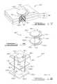
- a multi-beam antenna 10 ′′′, 10 . 5comprises an electromagnetic lens 12 and plurality of dielectric substrates 16 , each comprising a set of antenna feed elements 14 and operating in accordance with the description hereinabove.
- Each set of antenna feed elements 14generates (or is capable of generating) an associated set of beams of electromagnetic energy 20 . 1 , 20 . 2 and 20 . 3 , each having associated directions 42 . 1 , 42 . 2 and 42 . 3 , responsive to the associated feed 58 and control 60 signals.
- the associated feed 58 and control 60 signalsare either directly applied to the associated switch network 48 of the respective sets of antenna feed elements 14 , or are applied thereto through a second switch network 78 having associated feed 80 and control 82 ports, each comprising at least one associated signal. Accordingly, the multi-beam antenna 10 ′′′, 10 . 5 provides for transmitting or receiving one or more beams of electromagnetic energy over a three-dimensional space.
- the multi-beam antenna 10provides for a relatively wide field-of-view, and is suitable for a variety of applications, including but not limited to automotive radar, point-to-point communications systems and point-to-multi-point communication systems, over a wide range of frequencies for which the antenna feed elements 14 may be designed to radiate, for example, frequencies in the range of 1 to 200 GHz.
- the multi-beam antenna 10may be configured for either mono-static or bi-static operation.
- a dielectric electromagnetic lens 12When relatively a narrow beamwidth, i.e. a high gain, is desired at a relatively lower frequency, a dielectric electromagnetic lens 12 can become relatively large and heavy.
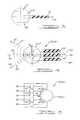
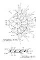
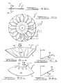
- the dielectric electromagnetic lens 12may be replaced with a discrete lens array 100 , e.g. a planar lens 100 . 1 , which can beneficially provide for setting the polarization, the ratio of focal length to diameter, and the focal surface shape, and can be more readily be made to conform to a surface.
- a discrete lens array 100can also be adapted to incorporate amplitude weighting so as to provide for control of sidelobes in the associates beams of electromagnetic energy 20 .
- the dielectric electromagnetic lens 12 of the first embodiment of the multi-beam antenna 10 , 10 . 1 illustrated in FIGS. 1 and 2is replaced with a planar lens 100 . 1 comprising a first set of patch antennas 102 . 1 on a first side 104 of the planar lens 100 . 1 , and a second set of patch antennas 102 . 2 on the second side 106 of the planar lens 100 . 1 , where the first 104 and second 106 sides are opposite one another.
- each patch antenna 102 , 102 . 1 on the first side 104 of the planar lens 100 . 1is operatively coupled via a delay element 108 to a corresponding patch antenna 102 , 102 . 2 on the second side 106 of the planar lens 100 . 1 , wherein the patch antenna 102 , 102 . 1 on the first side 104 of the planar lens 100 . 1 is substantially aligned with the corresponding patch antenna 102 , 102 . 2 on the second side 106 of the planar lens 100 . 1 .
- electromagnetic energy that is radiated upon one of the patch antennas 102e.g. a first patch antenna 102 . 1 on the first side 104 of the planar lens 100 . 1
- a signal responsive theretois coupled via—and delayed by—the delay element 108 to the corresponding patch antenna 102 , e.g. the second patch antenna 102 . 2 , wherein the amount of delay by the delay element 108 is dependent upon the location of the corresponding patch antennas 102 on the respective first 104 and second 106 sides of the planar lens 100 . 1 .
- the signal coupled to the second patch antenna 102 . 2is then radiated thereby from the second side 106 of the planar lens 100 . 1 .
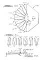
- the planar lens 100 . 1comprises a plurality of lens elements 110 , wherein each lens element 110 comprises a first patch antenna element 102 . 1 operatively coupled to a corresponding second patch antenna element 102 . 2 via at least one delay element 108 , wherein the first 102 . 1 and second 102 . 2 patch antenna elements are substantially opposed to one another on opposite sides of the planar lens 100 . 1 .
- the patch antennas 102 . 1 , 102 . 2comprise conductive surfaces on a dielectric substrate 112
- the delay element 108 coupling the patch antennas 102 . 1 , 102 . 2 of the first 104 and second 106 sides of the planar lens 100 . 1comprise delay lines 114 , e.g. microstrip or stipline structures, that are located adjacent to the associated patch antennas 102 . 1 , 102 . 2 on the underlying dielectric substrate 112 .
- the first ends 116 . 1 of the delay lines 114are connected to the corresponding patch antennas 102 .
- FIGS. 15 a and 15 billustrate the delay lines 114 arranged so as to provide for feeding the associated first 102 . 1 and second 102 . 2 sets of patch antennas at the same relative locations.
- the amount of delay caused by the associated delay elements 108is made dependent upon the location of the associated patch antenna 102 in the planar lens 100 . 1 , and, for example, is set by the length of the associated delay lines 114 , as illustrated by the configuration illustrated in FIGS. 15 a and 15 b , so as to emulate the phase properties of a convex electromagnetic lens 12 , e.g. a spherical lens 12 ′.
- the shape of the delay profile illustrated in FIG. 16can be of various configurations, for example, 1) uniform for all radial directions, thereby emulating a spherical lens 12 ′; 2) adapted to incorporate an azimuthal dependence, e.g. so as to emulate an elliptical lens; or 3) adapted to provide for focusing in one direction only, e.g. in the elevation plane of the multi-beam antenna 10 . 6 , e.g. so as to emulate a cylindrical lens.
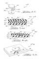
- a first embodiment of a lens element 110 I of the planar lens 100 . 1 illustrated in FIGS. 15 a and 15 bcomprises first 102 . 1 and second 102 . 2 patch antenna elements on the outer surfaces of a core assembly 120 comprising first 112 . 1 and second 112 . 2 dielectric substrates on both sides of a conductive ground plane 122 sandwiched therebetween.
- a first delay line 114 . 1 on the first side 104 of the planar lens 100 . 1extends circumferentially from a first location 124 . 1 on the periphery of the first patch antenna element 102 . 1 to a first end 118 .
- the combination of the first 114 . 1 and second 114 . 2 delay lines interconnected by the conductive via 118constitutes the associated delay element 108 of the lens element 110 , and the amount of delay of the delay element 108 is generally responsive to the cumulative circumferential lengths of the associated first 114 . 1 and second 114 . 2 delay lines and the conductive via 118 .
- the first 102 . 1 and second 102 . 2 patch antenna elementsmay be interconnected with one another so as to provide for dual polarization, for example, as disclosed in the technical paper “Multibeam Antennas with Polarization and Angle Diversity” by Darko Popovic and Zoya Popovic in IEEE Transactions on Antenna and Propagation , Vol. 50, No. 5, May 2002, which is incorporated herein by reference.
- a first location 126 . 1 on an edge of the first patch antenna element 102 . 1is connected via first 128 . 1 and second 128 . 2 delay lines to a first location 130 .
- first 128 . 1 and second 128 . 2 delay linesare interconnected with a first conductive via 132 . 1 that extends through associated first 134 .
- the first location 126 . 1 on the first patch antenna element 102 . 1is shown substantially orthogonal to the first location 130 . 1 on the second patch antenna element 102 . 2 so that the polarization of the radiation from the second patch antenna element 102 . 2 is orthogonal with respect to that of the radiation incident upon the first patch antenna element 102 . 1 .
- the first locations 126 . 1 and 130 . 1could be aligned with one another, or could be oriented at some other angle with respect to one another.
- one or more delay lines 114may be located between the first 102 . 1 and second 102 . 2 patch antenna elements—rather than adjacent thereto as in the first and second embodiments of the lens element 110 I , 110 II —so that the delay lines 114 are shadowed by the associated first 102 . 1 and second 102 . 2 patch antenna elements.
- the first patch antenna element 102 . 1 on a first side 136 . 1 of a first dielectric substrate 136is connected with a first conductive via 138 . 1 through the first dielectric substrate 136 to a first end 140 .
- a third conductive via 138 . 3interconnects the second ends 140 . 2 , 146 .
- first 140 and second 146 delay linesextends through the second 142 and fourth 148 dielectric substrates, and through a conductive ground plane 150 located between the second sides 142 . 2 , 148 . 2 of the second 142 and fourth 148 dielectric substrates.
- the first 140 and second 146 delay linesare shadowed by the first 102 . 1 and second 102 . 2 patch antenna elements, and therefore do not substantially affect the respective radiation patterns of the first 102 . 1 and second 102 . 2 patch antenna elements.
- the delay element 108may comprise at least one transmission line comprising either a stripline, a microstrip line, an inverted microstrip line, a slotline, an image line, an insulated image line, a tapped image line, a coplanar stripline, or a coplanar waveguide line formed on the dielectric substrate(s) 112 , 112 . 1 , 112 . 2 , for example, from a printed circuit board, for example, by subtractive technology, for example, chemical or ion etching, or stamping; or additive techniques, for example, deposition, bonding or lamination.
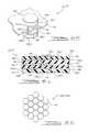
- the patch antennas 102are hexagonally shaped so as to provide for a more densely packed discrete lens array 100 ′.
- the particular shape of the individual patch antennas 102is not limiting, and for example, can be circular, rectangular, square, triangular, pentagonal, hexagonal, or some other polygonal shape or an arbitrary shape.
- FIGS. 13 , 15 a , 15 b , and 17 - 21illustrate a plurality of delay lines 114 . 1 , 114 . 2 , 128 . 1 , 128 . 2 , 128 . 3 , 128 . 4 , 140 , 146 interconnecting the first 102 . 1 and second 102 . 2 patch antenna elements
- a single delay line 114e.g. located on a surface of one of the dielectric substrates 112 , 134 , 136 , 142 , 144 —could be used, interconnected to the first 102 . 1 and second 102 . 2 patch antenna elements with associated conductive paths.
- the first 102 . 1 and second 102 . 2 patch antenna elementsare interconnected with a delay line 152 located therebetweeen, wherein a first end 152 . 1 of the delay line 152 is connected with a first conductive via 154 . 1 to the first patch antenna element 102 . 1 and a second end 152 . 2 of the delay line 152 is connected with a second conductive via 154 . 2 to the second patch antenna element 102 . 2 .
- FIG. 24 ain accordance with a third embodiment of a planar lens 100 .
- the first patch antenna element 102 . 1is located on a first side 156 . 1 of a first dielectric substrate 156
- the second patch antenna element 102 . 2is located on a first side 158 . 1 of a second dielectric substrate 158
- the delay line 152is located between the second side 156 . 2 of the first dielectric substrate 156 and a first side 160 . 1 of a third dielectric substrate 160 and the first conductive via 154 . 1 extends through the first dielectric substrate 156 .
- a conductive ground plane 162is located between the second sides 158 . 2 , 160 .
- a fourth embodiment of a planar lens 100 . 4incorporates the fourth embodiment of a lens element 110 IV′′ illustrated in FIG. 23 , without the third dielectric substrate 160 of the third embodiment of the planar lens 100 . 3 illustrated in FIG. 24 a , wherein the delay line 152 and the conductive ground plane 162 are coplanar between the second sides 156 . 2 , 158 . 2 of the first 156 and second 158 dielectric substrates, and are insulated or separated from one another.
- the discrete lens array 100does not necessarily have to incorporate a conductive ground plane 122 , 136 , 150 , 162 .
- the conductive ground plane 162is optional, particularly if a closely packed array of patch antennas 102 were used as illustrated in FIG. 22 .
- the first embodiment of a lens element 110 I illustrated in FIG. 18could be constructed with the first 102 . 1 and second 102 . 2 patch antenna elements on opposing sides of a single dielectric substrate 112 .
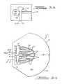
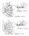
- a reflective discrete lens array 164comprises a plurality of patch antennas 102 located on a first side 166 . 1 of a dielectric substrate 166 and connected via corresponding delay lines 168 that are terminated either with an open or short circuit, e.g. by termination at an associated conductive ground plane 170 on the second side 166 . 2 of the dielectric substrate 166 , wherein the associated delays of the delay lines 168 are adapted—for example, as illustrated in FIG.
- the reflective discrete lens array 164acts as a reflector and provides for receiving electromagnetic energy in the associated patch antennas 102 , and then reradiating the electromagnetic energy from the patch antennas 102 after an associated location dependent delay, so as to provide for focusing the reradiated electromagnetic energy in a desired direction responsive to the synthetic structure formed by the phase front of the reradiated electromagnetic energy responsive to the location dependent delay lines.
- the discrete lens array 100 . 5comprises an assembly of a first set 300 . 1 of first broadside antenna elements 302 . 1 on a first side 304 . 1 of the discrete lens array 100 . 5 , and a corresponding second set 300 . 2 of second broadside antenna elements 302 . 2 on a second side 304 . 2 of the discrete lens array 100 . 5 , wherein the first 304 . 1 and second 304 . 2 sides face in opposing directions with respect to one another, and the first 302 . 1 and second 302 .
- first 302 . 1 and second 302 . 2 broadside antenna elements of each pair 306are adapted to communicate with one another through an associated delay element 108 , wherein the amount of delay, or phase shift, is a function of the location of the particular pair 306 of first 302 . 1 and second 302 . 2 broadside antenna elements in the discrete lens array 100 . 5 so as to emulate the behavior of an electromagnetic lens, for example, a spherical, plano-spherical, elliptical, cylindrical or plano-cylindrical lens.
- the delayas a function of location on the discrete lens array 100 .
- a transmit modefor transforming a diverging beam of beam of electromagnetic energy 20 from an associated antenna element 14 at a focal point to a corresponding substantially collimated beam exiting the discrete lens array 100 . 5 ; and vice versa in a receive mode.
- first set 300 . 1 of first broadside antenna elements 302 . 1are located on a first side 308 . 1 of a first dielectric substrate 308 and the second set 300 . 2 of second broadside antenna elements 302 . 2 , for example, patch antenna elements, are located on a first side 310 . 1 of a second dielectric substrate 310 , with the respective second sides 308 . 2 , 310 . 2 of the first 308 and second 310 dielectric substrates facing one another across opposing sides of a central conductive layer 312 that is provided with associated coupling slots 314 associated with each pair 306 of first 302 . 1 and second 302 .
- the coupling slots 314are “U-shaped”—i.e. similar to the end of a tuning fork—and in cooperation with the adjacent first 308 and second 310 dielectric substrates constitute a sandwiched coplanar-waveguide (CPW) resonant structure, wherein the associated phase delay can be adjusted by scaling the associated coupling slot 314 , and/or adjusting the position of the coupling slot 314 relative to the associated first 302 . 1 and second 302 . 2 broadside antenna elements.
- CPWcoplanar-waveguide
- first 302 . 1 and second 302 . 2 broadside antenna elements in combination with an associated delay element 108constitute a bandpass filter with radiative ports which can each be modeled as a three-pole filter based upon the corresponding three resonators of the associated first 302 . 1 and second 302 . 2 broadside antenna elements and the associated coupling slot 314 .
- This arrangementis also known as an Antenna-Filter-Antenna (AFA) configuration.
- AFAAntenna-Filter-Antenna
- the first 308 and second 310 dielectric substratesmay be constructed of a material with relatively low loss at an operating frequency, examples of which include DUROID®, a TEFLON® containing material, a ceramic material, depending upon the frequency of operation.
- the first 308 and second 310 dielectric substratescomprise DUROID® with a TEFLON® substrate of about 15-20 mil thickness and a relative dielectric constant of about 2.2, wherein the first 302 . 1 and second 302 .
- first 302 . 1 and second 302 . 2 broadside antenna elementsmay, for example, comprise microstrip patches, dipoles or slots.
- the patch antennas/patch antenna elements 102 . 1 , 102 . 2 of above-described lens elements 110 , 110 I - 110 V of the above-described discrete lens arrays 100 , 100 . 1 - 100 . 4could in general be broadside antennas/broadside antenna elements 302 . 1 , 302 . 2 , the latter of which may, for example, comprise microstrip patches, dipoles or slots.
- the discrete lens array 100 , 164is adapted to cooperate with a plurality of antenna feed elements 14 , e.g. end-fire antenna element 14 .
- antenna feed elements 14located along the edge of a dielectric substrate 16 having an edge contour 30 adapted to cooperate with the focal surface of the associated discrete lens array 100 , 164 , wherein the antenna feed elements 14 are fed with a feed signal 28 coupled thereto through an associated switching network 48 , whereby one or a combination of antenna feed elements 14 may be fed so as to provide for one or more beams of electromagnetic energy 20 , the direction of which can be controlled responsive to a control signal 60 applied to the switching network 48 .
- the discrete lens array 100can be adapted to cooperate with a plurality of dielectric substrates 16 , each comprising a set of antenna feed elements 14 and operating in accordance with the description hereinabove.
- Each set of antenna feed elements 14generates or receives (or is capable of generating or receiving) an associated set of beams of electromagnetic energy 20 . 1 , 20 . 2 and 20 . 3 , each having associated directions 42 . 1 , 42 . 2 and 42 .
- the multi-beam antenna 10 . 8provides for transmitting or receiving one or more beams of electromagnetic energy over a three-dimensional space.
- any of the above-described antenna embodimentscan be used for either transmission or reception or both transmission and reception of electromagnetic energy.
- the discrete lens array 100 , 164 in combination with planar, end-fire antenna elements 14 . 1 etched on a dielectric substrate 16provides for a multi-beam antenna 10 that can be manufactured using planar construction techniques, wherein the associated antenna feed elements 14 and the associated lens elements 110 are respectively economically fabricated and mounted as respective groups, so as to provide for an antenna system that is relatively small and relatively light weight.
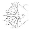
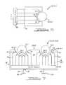
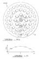
- a multi-beam antenna 10 ivcomprises a dielectric substrate 16 having a convex profile 202 —e.g. circular, semi-circular, quasi-circular, elliptical, or some other profile shape as may be required—with a plurality of end-fire antenna elements 14 . 1 etched into a first conductive layer 36 . 1 on the first side 16 . 1 of the dielectric substrate 16 .
- the plurality of end-fire antenna elements 14.
- the end-fire antenna elements 14 . 1are illustrated as abutting the convex profile 202 .
- the dielectric substrate 16is, for example, a material with relatively low loss at an operating frequency, for example, DUROID®, a TEFLON® containing material, a ceramic material, or a composite material such as an epoxy/fiberglass composite.
- the dielectric substrate 16comprises a dielectric 16 ′ of a circuit board 34 , for example, a printed or flexible circuit 34 . 1 ′ comprising at least one conductive layer 36 adhered to the dielectric substrate 16 , from which the end-fire antenna elements 14 . 1 and other associated circuit traces 38 are formed, for example, by subtractive technology, for example, chemical or ion etching, or stamping; or additive techniques, for example, deposition, bonding or lamination.
- the multi-beam antenna 10 iv illustrated in FIGS. 30 , 34 and 35was fabricated on an RT/DUROID® 5880 substrate with a copper layer of 17 micrometers thickness on either side with a fabrication process using a one-mask process with one lithography step.
- An end-fire antenna element 14 . 1may, for example, comprise either a Yagi-Uda antenna, a coplanar horn antenna (also known as a tapered slot antenna), a Vivaldi antenna, a tapered dielectric rod, a slot antenna, a dipole antenna, or a helical antenna, each of which is capable of being formed on the dielectric substrate 16 , for example, from a printed or flexible circuit 34 . 1 ′, for example, by subtractive technology, for example, chemical or ion etching, or stamping; or additive techniques, for example, deposition, bonding or lamination.
- the end-fire antenna element 14may, for example, comprise either a Yagi-Uda antenna, a coplanar horn antenna (also known as a tapered slot antenna), a Vivaldi antenna, a tapered dielectric rod, a slot antenna, a dipole antenna, or a helical antenna, each of which is capable of being formed on the dielectric substrate 16 , for example
- a monopole antennafor example, a monopole antenna element oriented either in-plane or out-of-plane with respect to the dielectric substrate 16 .
- the end-fire antenna elements 14 . 1may be used for transmitting, receiving or both.
- the embodiments illustrated in FIGS. 28 and 30incorporate tapered-slot antennas 14 . 1 ′ as the associated end-fire antenna elements 14 . 1 .
- the tapered-slot antenna 14 . 1 ′is a surface-wave traveling-wave antenna, which generally allows wider band operation in comparison with resonant structures, such as dipole or Yagi-Uda antennas.
- the directivity of a traveling-wave antennadepends mostly upon length and relatively little on its aperture.
- the apertureis typically larger than a half free space wavelength to provide for proper radiation and low reflection.
- the input impedancebecomes mismatched with respect to that of an associated slotline feed and considerable reflections may occur. Longer antennas generally provide for increased directivity. Traveling-wave antennas generally are substantially less susceptible to mutual coupling than resonant antennas, which makes it possible to place them in close proximity to each other without substantially disturbing the radiation pattern of the associated multi-beam antenna 10 iv .
- the tapered-slot antenna 14 . 1 ′comprises a slot in a conductive ground plane supported by a dielectric substrate 16 .
- the width of the slotincreases gradually in a certain fashion from the location of the feed to the location of interface with free space. As the width of the slot increases, the characteristic impedance increases as well, thus providing a smooth transition to the free space characteristic impedance of 120 times pi Ohms.
- FTSAFermi tapered slot antenna
- LTSAlinearly tapered slot antenna
- the tapered-slot antenna 14 . 1 ′exhibits an E-field polarization that is in the plane of the tapered-slot antenna 14 . 1 ′.
- tapered-slot antennas 14 . 1 ′exhibit corresponding different radiation patterns, also depending on the length and aperture of the slot and the supporting substrate.
- the beamwidthis smallest for the CWSA, followed by the LTSA, and then the Vivaldi.
- the sidelobesare highest for the CWSA, followed by the LTSA, and then the Vivaldi.
- the Vivaldihas theoretically the largest bandwidth due to its exponential structure.
- the BLTSAexhibits a wider ⁇ 3 dB beamwidth than the LTSA and the cross-polarization in the D-plane (diagonal plane) is about 2 dB lower compared to LTSA and CWSA.
- the DETSAhas a smaller ⁇ 3 dB beamwidth than the Vivaldi, but the sidelobe level is higher, although for higher frequency, the sidelobes can be suppressed.
- the DETSAgives an additional degree of freedom in design especially with regard to parasitic effects due to packaging.
- the FTSAexhibits very low and the most symmetrical sidelobe level in E and H-plane and the ⁇ 3 dB beamwidth is larger than the BLTSA.
- the multi-beam antenna 10 ivmay further comprise at least one transmission line 44 on the dielectric substrate 16 operatively connected to a corresponding at least one feed port 46 of a corresponding at least one of the plurality of end-fire antenna elements 14 . 1 for feeding a signal thereto or receiving a signal therefrom.
- the at least one transmission line 44may comprise either a stripline, a microstrip line, an inverted microstrip line, a slotline, an image line, an insulated image line, a tapped image line, a coplanar stripline, or a coplanar waveguide line formed on the dielectric substrate 16 , for example, of a printed or flexible circuit 34 . 1 ′, for example, by subtractive technology, for example, chemical or ion etching, or stamping; or additive techniques, for example, deposition, bonding or lamination.
- each of the tapered-slot endfire antenna elements 14 . 1 ′interface with an associated slotline 204 by which energy is coupled to or from the tapered-slot endfire antenna element 14 . 1 ′.
- the slotlines 204are terminated with at a terminus 206 on the first side 16 . 1 of the dielectric substrate 16 , proximate to which the slotlines 204 is electromagnetically coupled at a coupling location 208 to a microstrip line 210 on the opposite or second side 16 . 2 of the dielectric substrate 16 , wherein the first conductive layer 36 . 1 on the first side 16 .
- the dielectric substrate 16constitutes an associated conductive ground layer 212 of the microstrip line 210
- the conductor 214 of the microstrip line 210is formed from a second conductive layer 36 . 2 on the second side 16 . 2 of the dielectric substrate 16 .
- a transition between the microstrip line 210 and the slotline 204is formed by etching the slotline 204 into the conductive ground layer 212 of the microstrip line 210 and is crossed by the conductor 214 of the microstrip line 210 oriented substantially perpendicular to the axis of the slotline 204 , as is illustrated in detail in FIG. 33 .
- a transition distance of about one wavelengthprovides matching the 50 Ohm impedance of the microstrip line 210 to the 100 Ohm impedance of the slotline 204 .
- the coupling of the fields between the microstrip line 210 and slotline 204occurs through an associated magnetic field, and is strongest when the intersection of the conductor 214 and slotline 204 occurs proximate to a short circuit of the microstrip line 210 —where the current therein is a maximum—and an open circuit of the slotline 204 . Because short circuits in a microstrip line 210 require via holes, it is easier to terminate the microstrip line 210 in an open circuit a quarter guided wavelength from the transition intersection, where quarter guided wavelength is that of the microstrip line 210 . A quarter-wave radial stub 216 can provide for relatively wider bandwidth.
- An open circuit in the slotline 204is created by truncating the conductive ground layer 212 , which is generally impractical.
- the slotline 204is terminated with a short circuit and recessed from the intersection by a quarter guided wavelength of the slotline 204 .
- the bandwidthcan be increased by realizing the quarter-wave termination in a circular disc aperture 218 , which is an approximation of an open circuit of a slotline 204 .
- the open-circuit behaviorimproves with increasing radius of the circular disc aperture 218 .
- the circular disc aperture 218behaves like a resonator.
- the circular disc aperture 218is capacitive in nature, and behaves as an open circuit provided that the operating frequency is higher than the resonance frequency of the circular disc aperture 218 resonator.
- the multi-beam antenna 10 ivmay further comprise a switching network 48 having at least one first port 50 ′ and a plurality of second ports 52 ′, wherein the at least one first port 50 ′ is operatively connected—for example, via at least one above described transmission line 44 —to a corporate antenna feed port 54 , and each second port 52 ′ of the plurality of second ports 52 ′ is connected—for example, via at least one transmission line 44 —to a respective feed port 46 of a different end-fire antenna element 14 . 1 of the plurality of end-fire antenna elements 14 . 1 .
- the switching network 48further comprises at least one control port 56 for controlling which second ports 52 ′ are connected to the at least one first port 50 ′ at a given time.
- the switching network 48may, for example, comprise either a plurality of micro-mechanical switches, PIN diode switches, transistor switches, or a combination thereof, and may, for example, be operatively connected to the dielectric substrate 16 , for example, by surface mount to an associated conductive layer 36 of a printed or flexible circuit 34 . 1 ′, inboard of the end-fire antenna elements 14 . 1 .
- the switching network 48may be located proximate to the center 220 of the radius R of curvature of the dielectric substrate 16 so as to be proximate to the associated coupling locations 208 of the associated microstrip lines 210 .
- the switching network 48if used, need not be collocated on a common dielectric substrate 16 , but can be separately located, as, for example, may be useful for relatively lower frequency applications, for example, 1-20 GHz.
- a feed signal 58 applied to the corporate antenna feed port 54is either blocked—for example, by an open circuit, by reflection or by absorption,—or switched to the associated feed port 46 of one or more end-fire antenna elements 14 . 1 , via one or more associated transmission lines 44 , by the switching network 48 , responsive to a control signal 60 applied to the control port 56 .
- the feed signal 58may either comprise a single signal common to each end-fire antenna element 14 . 1 , or a plurality of signals associated with different end-fire antenna elements 14 . 1 .
- Each end-fire antenna element 14 . 1 to which the feed signal 58 is appliedlaunches an associated electromagnetic wave into space. The associated beams of electromagnetic energy 20 launched by different end-fire antenna elements 14 .
- the various beams of electromagnetic energy 20may be generated individually at different times so as to provide for a scanned beam of electromagnetic energy 20 . Alternatively, two or more beams of electromagnetic energy 20 may be generated simultaneously.
- different end-fire antenna elements 14 . 1may be driven by different frequencies that, for example, are either directly switched to the respective end-fire antenna elements 14 . 1 , or switched via an associated switching network 48 having a plurality of first ports 50 ′, at least some of which are each connected to different feed signals 58 .
- the multi-beam antenna 10 ivmay be adapted so that the respective signals are associated with the respective end-fire antenna elements 14 . 1 in a one-to-one relationship, thereby precluding the need for an associated switching network 48 .
- each end-fire antenna element 14 . 1can be operatively connected to an associated signal through an associated processing element.
- the respective end-fire antenna elements 14 . 1are used to receive electromagnetic energy, and the corresponding processing elements comprise detectors.
- the respective end-fire antenna elements 14 . 1are used to both transmit and receive electromagnetic energy, and the respective processing elements comprise transmit/receive modules or transceivers.
- a multi-beam antenna 10 ivis adapted with a plurality of detectors 224 for detecting signals received by associated end-fire antenna elements 14 . 1 of the multi-beam antenna 10 iv , for example, to provide for making associated radiation pattern measurements.
- Each detector 224comprises a planar silicon Schottky diode 224 . 1 mounted with an electrically conductive epoxy across a gap 226 in the microstrip line 210 .
- the diode 224 . 1is DC-biased.
- Two quarter wavelength-stub filters 228provide for maximizing the current at the location of the diode detector 224 . 1 while preventing leakage into the DC-path.
- FIG. 37illustrates an E-plane radiation pattern for the multi-beam antenna 10 iv illustrated in FIGS. 30 and 35 , configured as a receiving antenna.
- the tapered-slot endfire antenna elements 14 . 1 ′provide for relatively narrow individual E-plane beam-widths, but inherently exhibit relatively wider H-plane beam-widths, of the associated beams of electromagnetic energy 20 .
- the H-plane beam-widthmay be reduced, and the directivity of the multi-beam antenna 10 iv may be increased, by sandwiching the above-described multi-beam antenna 10 iv within a bi-conical reflector 230 , so as to provide for a horn-like antenna in the H-plane.
- the opening angle between the opposing faces 232 of the bi-conic reflectoris about ninety (90) degrees and the lateral dimensions coincide with that of the dielectric substrate 16 .
- the measured radiation patterns in E-plane of this embodimentexhibited a ⁇ 3 dB beamwidth of 26 degrees and the cross-over of adjacent beams occurs at the ⁇ 2.5 dB level.
- the sidelobe levelwas about ⁇ 6 dB, and compared to the array without a reflector, the depth of the nulls between main beam and sidelobes was substantially increased.
- the ⁇ 3 and ⁇ 10 dB beamwidthswere 35 degrees and 68 degrees respectively, respectively, and the sidelobe level was below ⁇ 20 dB.
- the presence of the bi-conical reflector 230increased the measured gain by 10 percent. Although the improvement in gain is relatively small, e.g. about 10 percent, the bi-conical reflector 230 is beneficial to the H-plane radiation pattern.
- the H-plane beam-widthmay be reduced, and the directivity of the multi-beam antenna 10 iv may be increased, by using a conformal cylindrical dielectric lens 234 which is bent along its cylindrical axis so as to conform to the convex profile 202 of the dielectric substrate 16 , so as to provide for focusing in the H-plane without substantially affecting the E-plane radiation pattern.
- the conformal cylindrical dielectric lens 234could be constructed from either RexoliteTM, TeflonTM, polyethylene, or polystyrene; or a plurality of different materials having different refractive indices.
- the conformal cylindrical dielectric lens 234could have a plano-cylindrical cross-section, rather than the circular cross-section as illustrated in FIG. 39 b .
- the conformal cylindrical dielectric lens 234may be adapted to also act as a radome so as to provide for protecting the multi-beam antenna 10 vi from the adverse environmental elements (e.g. rain or snow) and factors, or contamination (e.g. dirt).
- the H-plane beam-widthmay be reduced, and the directivity of the multi-beam antenna 10 iv may be increased, by using a discrete lens array 236 , the surface (e.g. planar surface) of which is oriented normal to the dielectric substrate 16 and—in a direction normal to the surface of the discrete lens array 236 —is adapted to conform to the convex profile 202 of the dielectric substrate 16 .
- a discrete lens array 236the surface (e.g. planar surface) of which is oriented normal to the dielectric substrate 16 and—in a direction normal to the surface of the discrete lens array 236 —is adapted to conform to the convex profile 202 of the dielectric substrate 16 .
- the discrete lens array 236would comprise a plurality of first patch antennas 102 . 1 on one side of an associated dielectric substrate 112 of the discrete lens array 236 that are connected via associated delay elements 114 ′, e.g. delay lines 114 , to a corresponding plurality of second patch antennas 102 . 2 on the opposites side of the associated dielectric substrate 112 of discrete lens array 236 , wherein the length of the delay lines 114 decreases with increasing distance—in a direction that is normal to the dielectric substrate 16 —from the center 238 of the discrete lens array 236 which is substantially aligned with the dielectric substrate 16 .
- associated delay elements 114 ′e.g. delay lines 114
- the delay lines 114can be constructed by forming meandering paths of appropriate length using printed circuit technology.
- a cylindrical lens arrayis described by D. Popovic and Z. Popovic in “Mutlibeam Antennas with Polarization and Angle Diversity”, IEEE Transactions on Antennas and Propagation, Vol. 50, No. 5, May 2002, which is incorporated herein by reference.
- the patch antennas 102 . 1 , 102 . 2comprise conductive surfaces on the dielectric substrate 112
- the delay element 114 ′ coupling the patch antennas 102 . 1 , 102 . 2 of the first 236 . 1 and second 236 . 2 sides of the discrete lens array 236comprise delay lines 114 , e.g. microstrip or stipline structures, that are located adjacent to the associated patch antennas 102 . 1 , 102 . 2 on the underlying dielectric substrate 112 .
- the first ends 238 . 1 of the delay lines 114are connected to the corresponding patch antennas 102 . 1 , 102 .
- FIG. 41illustrates the delay lines 114 arranged so as to provide for feeding the associated first 102 . 1 and second 102 . 2 sets of patch antennas at the same relative locations.
- the discrete lens array 236is adapted in accordance with an Antenna-Filter-Antenna configuration, for example, in accordance with the fifth embodiment of the discrete lens array 100 . 5 incorporating the sixth embodiment of the associated lens element 110 VI described hereinabove.
- the amount of delay caused by the associated delay lines 114is made dependent upon the location of the associated patch antenna 102 in the discrete lens array 236 , and, for example, is set by the length of the associated delay lines 114 , as illustrated by the configuration illustrated in FIG. 41 , so as to emulate the phase properties of a convex electromagnetic lens, e.g. a conformal cylindrical dielectric lens 234 .
- the shape of the delay profile illustrated in FIG. 42can be of various configurations, for example, 1) uniform for all radial directions, thereby emulating a spherical lens; 2) adapted to incorporate an azimuthal dependence, e.g.
- the dielectric substrate 16 with a plurality of associated end-fire antenna elements 14 . 1is combined with associated out-of-plane reflectors 240 above and below the dielectric substrate 16 , in addition to any that are etched into the dielectric substrate 16 itself, so as to provide for improved the radiation patterns of the etched end-fire antenna elements 14 . 1 .
- a dipole antenna 14 . 2 and an associated reflector portion 242can be etched in at least one conductive layer 36 on the dielectric substrate 16 .
- a Yagi-Uda elementcould used instead of the dipole antenna 14 . 2 .
- the etched reflector portion 242can also be extended away from the dielectric substrate 16 to form a planar corner reflector 244 , e.g. by attaching relatively thin conductive plates 246 to the associated first 36 . 1 and second 36 . 2 conductive layers, e.g. using solder or conductive epoxy. For example, this would be similar to the metallic enclosures currently used to limit electromagnetic emissions and susceptibility on circuit boards.
- the planar corner reflectors 244are each illustrated at an included angle of about forty-five (45) degrees relative to the associated conductive layers 36 on the dielectric substrate 16 .
- the reflectors 240could also be made of solid pieces that span across all of the end-fire antenna elements 14 .
- the multi-beam antenna 10 viiimay be adapted with fewer than two reflector portions 242 , for example, one or none, wherein the associated dipole antenna 14 . 2 , or alternative Yagi-Uda element, would then cooperate with the associated reflector portion 242 and, if present, one of the conductive plates 246 .
- a Yagi-Uda antenna 14 . 3may be used as an end-fire antenna element 14 . 1 of a multi-beam antenna 10 iv , as described in “A 24-GHz High-Gain Yagi-Uda Antenna Array” by P. R. Grajek, B. Schoenlinner and G. M. Rebeiz in Transactions on Antennas and Propagation, May, 2004, which is incorporated herein by reference.
- a Yagi-Uda antenna 14 . 3incorporates a dipole element 248 , two forward director elements 250 on the first side 16 . 1 of the dielectric substrate 16 —e.g.
- the dimensionsare then scaled to compensate for the affects of the DUROID® substrate, e.g. so as to provide for the correct resonant frequency.
- the feed gap Swas limited to a width of 0.15 mm due to the resolution of the etching process.
- the Yagi-Uda antenna 14 . 3is fed with a microstrip line 210 coupled to a coplanar stripline 256 coupled to the Yagi-Uda antenna 14 . 3 .
- a microstrip line 210coupled to a coplanar stripline 256 coupled to the Yagi-Uda antenna 14 . 3 .
- the transition between the microstrip line 210 and the coplanar stripline 256is provided by splitting the primary microstrip line 210 into two separate coplanar stripline 256 , one of which incorporates a balun 258 comprising a meanderline 260 of sufficient length to cause a 180 degree phase shift, so as to provide for exciting a quasi-TEM mode along the balanced coplanar striplines 256 connected to the dipole element 248 .
- a quarter-wave transformer section 262 between the microstrip line 210 and the coplanar striplines 256provides for matching the impedance of the coplanar stripline 256 /Yagi-Uda antenna 14 . 3 to that of the microstrip line 210 .
- the input impedanceis affected by the gap spacing Sm of the meanderline 260 through mutual coupling in the balun 258 , and by the proximity S T of the meanderline 260 to the edge 264 of the associated ground plane 266 , wherein fringing effects can occur if the meanderline 260 of the is too close to the edge 264 .
- the Yagi-Uda antenna 14 . 3is used as a receiving antenna in cooperation with a second embodiment of an associated feed circuit 270 , wherein a detector 224 is operatively coupled across the coplanar striplines 256 from the associated dipole element 248 , and ⁇ g/4 open-stubs 272 are operatively coupled to each coplanar stripline 256 at a distance of ⁇ g/4 from the detector 224 , which provides for an RF open circuit at the detector 224 , and which provides for a detected signal at nodes 274 operatively coupled to the associated coplanar striplines 256 beyond the ⁇ g/4 open-stubs 272 .
- a multi-beam antenna 10 ixcomprises a dielectric substrate 16 having a concave profile 276 —e.g. circular, semi-circular, quasi-circular, elliptical, or some other profile shape as may be required—with a plurality of end-fire antenna elements 14 . 1 , for example, Yagi-Uda antennas 14 . 3 constructed in accordance with the embodiment illustrated in FIGS. 44 a and 44 b , with a second embodiment of the feed circuit 270 as illustrated in FIG.
- a concave profile 276e.g. circular, semi-circular, quasi-circular, elliptical, or some other profile shape as may be required
- end-fire antenna elements 14 . 1for example, Yagi-Uda antennas 14 . 3 constructed in accordance with the embodiment illustrated in FIGS. 44 a and 44 b , with a second embodiment of the feed circuit 270 as illustrated in FIG.
- the embodiment of the multi-beam antenna 10 ix illustrated in FIG. 47comprises an 11-element array of Yagi-Uda antennas 14 . 3 that are evenly spaced with an angular separation of 18.7 degrees so as to provide for an associated ⁇ 6 dB beam cross-over.
- the multi-beam antenna 10 ix of the tenth aspectis adapted to cooperate with an at least partially spherical electromagnetic lens 12 ′, for example, a spherical TEFLON® lens, so as to provide for improved directivity, for example, as disclosed in U.S. Pat. No. 6,424,319, which is incorporated herein by reference.
- an at least partially spherical electromagnetic lens 12 ′for example, a spherical TEFLON® lens
- the multi-beam antenna 10 ix of the tenth aspectis adapted to cooperate with a concave bi-conical reflector 280 , so as to provide for reducing the associated beam-width in the H-plane, for example, as disclosed hereinabove in accordance with the embodiment illustrated in FIGS. 38 a and 38 b .
- concave bi-conical reflector 280may be replaced with out-of-plane reflectors 240 , for example, as disclosed hereinabove in accordance with the embodiment illustrated in FIGS. 43 a and 43 b.
- the multi-beam antenna 10 ivcomprises a dielectric substrate 16 with a convex profile 202 , for example, a circular, quasi-circular or elliptical profile, wherein an associated plurality end-fire antenna elements 14 . 1 etched into a first conductive layer 36 . 1 on the first side 16 . 1 of the dielectric substrate 16 are distributed around the edge 282 of the dielectric substrate 16 so as to provide for omni-directional operation.
- the plurality of end-fire antenna elements 14.
- the end-fire antenna elements 14 . 1are adapted to radiate a corresponding plurality of beams of electromagnetic energy 20 radially outwards from the convex profile 202 of the dielectric substrate 16 , or to receive a corresponding plurality of beams of electromagnetic energy 20 propagating towards the convex profile 202 of the dielectric substrate 16 .
- the end-fire antenna elements 14 . 1are arranged so that the associated radiation patterns intersect one another at power levels ranging from ⁇ 2 dB to ⁇ 6 dB, depending upon the particular application.
- the number of end-fire antenna elements 14 . 1would depend upon the associated beamwidths and the associated extent of total angular coverall required, which can range from the minimum azimuthal extent covered by two adjacent end-fire antenna elements 14 . 1 to 360 degrees for full omni-directional coverage.
- the switching network 48is fabricated using either a single integrated circuit or a plurality of integrated circuits, for example, a 1:2 switch followed by two 1:4 switches.
- the switching network 48may comprise either GaAs P-I-N diodes, Si P-I-N diodes, GaAs MESFET transistors, or RF MEMS switches, the latter of which may provide for higher isolation and lower insertion loss.
- the associated transmission line 44may be adapted to beneficially reduce the electromagnetic coupling between different transmission lines 44 , for example by using either vertical co-axial feed transmission lines 44 , coplanar-waveguide transmission lines 44 , suspended stripline transmission lines 44 , or microstrip transmission lines 44 . Otherwise, coupling between the associated transmission lines 44 can degrade the associated radiation patterns of the associated end-fire antenna elements 14 . 1 so as to cause a resulting ripple in the associated main-lobes and increased associated sidelobe levels thereof.
- An associated radar unitcan be located directly behind the switch matrix on either the same dielectric substrate 16 (or on a different substrate), so as to provide for reduced size and cost of an associated radar system. The resulting omni-directional radar system could be located on top of a vehicle so as to provide full azimuthal coverage with a single associated multi-beam antenna 10 iv .
- the dielectric substrate 16can be angled in the vertical direction, either upward or downward in elevation, for example, so as to provide for eliminating or reducing associated ground reflections, also known as clutter.
- the dielectric substrate 16 of a multi-beam antenna 10 iv with a convex profile 202may be provided with a conical shape so that each of the associated end-fire antenna elements 14 .
- the dielectric substrate 16 of a multi-beam antenna 10 iv with a concave profile 276may be provided with a conical shape so that each of the associated end-fire antenna elements 14 . 1 is oriented with an elevation angle towards the associated axis 284 of the conical surface 286 , for example, so as to provide for orienting the associated directivity of the associated end-fire antenna elements 14 . 1 upwards in elevation. Accordingly, the dielectric substrate 16 of the multi-beam antenna 10 iv-xii need not be planar.
- a multi-beam antenna 10 xiiiis similar to the fifth and ninth aspects described hereinabove, except that the associated end-fire antenna elements 14 . 1 comprise a plurality of monopole antennas 14 . 4 that are coupled to, and which extend from, the associated circuit traces 38 on the first side 16 . 1 of the dielectric substrate 16 of the associated transmission lines 44 that provide for feeding the monopole antennas 14 . 4 from the associated switch network 48 .
- each circuit trace 38 in cooperation with the second conductive layer 36 . 2 on the second side 16 . 2 of the dielectric substrate 16constitutes a microstrip line 210 that provides the associated transmission line 44 .
- the monopole antennas 14 . 4extend, from the first side 16 . 1 of the dielectric substrate 16 , substantially normal to the second conductive layer 36 . 2 on the second side 16 . 2 of the dielectric substrate 16 , which cooperates therewith as an associated ground plane thereof.
- Each monopole antenna 14 . 4also cooperates with an associated corner reflector 244 . 1 that extends from, and is coupled to—e.g. using solder or conductive epoxy,—or a continuation of, the first conductive layer 36 . 1 on the first side 16 . 1 of the dielectric substrate 16 , which, for example, may also be electrically connected to the second conductive layer 36 . 2 on the second side 16 .
- each corner reflector 244 . 1provides for azimuthally shaping the radiation pattern of associated monopole antenna 14 . 4 , which is directed outwards, for example, radially outwards, from the convex profile 202 of the dielectric substrate 16 .
- an associated reflector portion 242is etched in the first conductive layer 36 . 1 proximate to each monopole antenna 14 . 4 , wherein the edge of the reflector portion 242 is aligned with the associated corner reflector 244 . 1 .
- a multi-beam antenna 10 xivis similar to the multi-beam antenna 10 xiii in accordance with the fourteenth aspect, except that instead of, or in addition to, the corner reflector 244 . 1 of the fourteenth aspect, a planar corner reflector 244 . 2 extending from the first side 16 . 1 of the dielectric substrate 16 and coupled to—e.g. using solder or conductive epoxy,—or a continuation of, the first conductive layer 36 . 1 , provides for shaping the elevation radiation pattern of each associated monopole antenna 14 . 4 .
- the planar corner reflector 244.
- planar corner reflector 244 . 2may be used alone, or in combination with the corner reflector 244 . 1 of the fourteenth aspect illustrated in FIGS. 53 a and 53 b , so as to provide for both shaping both the azimuthal and elevational radiation patterns of the associated monopole antenna 14 . 4 .
- the planar corner reflectors 244 . 2could also be integrated into a solid piece that spans across all of the monopole antennas 14 . 4 , using a common shape, such as for the bi-conical reflector 230 described hereinabove.
- the multi-beam antenna 10 iv-xivprovides for a relatively wide field-of-view, and is suitable for a variety of applications.
- the multi-beam antenna 10 iv-xivprovides for a relatively inexpensive, relatively compact, relatively low-profile, and relatively wide field-of-view, electronically scanned antenna for automotive applications, including, but not limited to, automotive radar for forward, side, and rear impact protection, stop and go cruise control, parking aid, and blind spot monitoring.
- the multi-beam antenna 10 iv-xivcan be used for point-to-point communications systems and point-to-multi-point communication systems, over a wide range of frequencies for which the end-fire antenna elements 14 . 1 may be designed to radiate, for example, 1 to 200 GHz.
- the multi-beam antenna 10 iv-xivmay be configured for either mono-static or bi-static operation.
Landscapes
- Engineering & Computer Science (AREA)
- Computer Security & Cryptography (AREA)
- Radar, Positioning & Navigation (AREA)
- Remote Sensing (AREA)
- Aerials With Secondary Devices (AREA)
Abstract
Description
Claims (9)
Priority Applications (3)
| Application Number | Priority Date | Filing Date | Title |
|---|---|---|---|
| US11/627,369US7994996B2 (en) | 1999-11-18 | 2007-01-25 | Multi-beam antenna |
| US11/929,791US7800549B2 (en) | 1999-11-18 | 2007-10-30 | Multi-beam antenna |
| US11/931,625US7605768B2 (en) | 1999-11-18 | 2007-10-31 | Multi-beam antenna |
Applications Claiming Priority (9)
| Application Number | Priority Date | Filing Date | Title |
|---|---|---|---|
| US16623199P | 1999-11-18 | 1999-11-18 | |
| US09/716,736US6424319B2 (en) | 1999-11-18 | 2000-11-20 | Multi-beam antenna |
| US10/202,242US6606077B2 (en) | 1999-11-18 | 2002-07-23 | Multi-beam antenna |
| US10/604,716US7042420B2 (en) | 1999-11-18 | 2003-08-12 | Multi-beam antenna |
| US52128404P | 2004-03-26 | 2004-03-26 | |
| US52207704P | 2004-08-11 | 2004-08-11 | |
| US10/907,305US20050219126A1 (en) | 2004-03-26 | 2005-03-28 | Multi-beam antenna |
| US11/161,681US7358913B2 (en) | 1999-11-18 | 2005-08-11 | Multi-beam antenna |
| US11/627,369US7994996B2 (en) | 1999-11-18 | 2007-01-25 | Multi-beam antenna |
Related Parent Applications (3)
| Application Number | Title | Priority Date | Filing Date |
|---|---|---|---|
| US10/604,716Continuation-In-PartUS7042420B2 (en) | 1999-11-18 | 2003-08-12 | Multi-beam antenna |
| US10/907,305Continuation-In-PartUS20050219126A1 (en) | 1999-11-18 | 2005-03-28 | Multi-beam antenna |
| US11/161,681Continuation-In-PartUS7358913B2 (en) | 1999-11-18 | 2005-08-11 | Multi-beam antenna |
Related Child Applications (2)
| Application Number | Title | Priority Date | Filing Date |
|---|---|---|---|
| US11/929,791ContinuationUS7800549B2 (en) | 1999-11-18 | 2007-10-30 | Multi-beam antenna |
| US11/931,625ContinuationUS7605768B2 (en) | 1999-11-18 | 2007-10-31 | Multi-beam antenna |
Publications (2)
| Publication Number | Publication Date |
|---|---|
| US20070195004A1 US20070195004A1 (en) | 2007-08-23 |
| US7994996B2true US7994996B2 (en) | 2011-08-09 |
Family
ID=38427653
Family Applications (3)
| Application Number | Title | Priority Date | Filing Date |
|---|---|---|---|
| US11/627,369Expired - Fee RelatedUS7994996B2 (en) | 1999-11-18 | 2007-01-25 | Multi-beam antenna |
| US11/929,791Expired - Fee RelatedUS7800549B2 (en) | 1999-11-18 | 2007-10-30 | Multi-beam antenna |
| US11/931,625Expired - Fee RelatedUS7605768B2 (en) | 1999-11-18 | 2007-10-31 | Multi-beam antenna |
Family Applications After (2)
| Application Number | Title | Priority Date | Filing Date |
|---|---|---|---|
| US11/929,791Expired - Fee RelatedUS7800549B2 (en) | 1999-11-18 | 2007-10-30 | Multi-beam antenna |
| US11/931,625Expired - Fee RelatedUS7605768B2 (en) | 1999-11-18 | 2007-10-31 | Multi-beam antenna |
Country Status (1)
| Country | Link |
|---|---|
| US (3) | US7994996B2 (en) |
Cited By (152)
| Publication number | Priority date | Publication date | Assignee | Title |
|---|---|---|---|---|
| US20120146842A1 (en)* | 2010-12-13 | 2012-06-14 | Electronics And Telecommunications Research Institute | Rf transceiver for radar sensor |
| WO2014193922A1 (en)* | 2013-05-28 | 2014-12-04 | University Of Florida Research Foundation, Inc. | Dual function helix antenna |
| WO2015006314A3 (en)* | 2013-07-08 | 2015-10-29 | L-Com, Inc. | Antennas |
| US9608740B2 (en) | 2015-07-15 | 2017-03-28 | At&T Intellectual Property I, L.P. | Method and apparatus for launching a wave mode that mitigates interference |
| US9615269B2 (en) | 2014-10-02 | 2017-04-04 | At&T Intellectual Property I, L.P. | Method and apparatus that provides fault tolerance in a communication network |
| US9628116B2 (en) | 2015-07-14 | 2017-04-18 | At&T Intellectual Property I, L.P. | Apparatus and methods for transmitting wireless signals |
| US9640850B2 (en) | 2015-06-25 | 2017-05-02 | At&T Intellectual Property I, L.P. | Methods and apparatus for inducing a non-fundamental wave mode on a transmission medium |
| US9667317B2 (en) | 2015-06-15 | 2017-05-30 | At&T Intellectual Property I, L.P. | Method and apparatus for providing security using network traffic adjustments |
| US9674711B2 (en) | 2013-11-06 | 2017-06-06 | At&T Intellectual Property I, L.P. | Surface-wave communications and methods thereof |
| US9685992B2 (en) | 2014-10-03 | 2017-06-20 | At&T Intellectual Property I, L.P. | Circuit panel network and methods thereof |
| US9692101B2 (en) | 2014-08-26 | 2017-06-27 | At&T Intellectual Property I, L.P. | Guided wave couplers for coupling electromagnetic waves between a waveguide surface and a surface of a wire |
| US9699785B2 (en) | 2012-12-05 | 2017-07-04 | At&T Intellectual Property I, L.P. | Backhaul link for distributed antenna system |
| US9705610B2 (en) | 2014-10-21 | 2017-07-11 | At&T Intellectual Property I, L.P. | Transmission device with impairment compensation and methods for use therewith |
| US9705561B2 (en) | 2015-04-24 | 2017-07-11 | At&T Intellectual Property I, L.P. | Directional coupling device and methods for use therewith |
| US9722318B2 (en) | 2015-07-14 | 2017-08-01 | At&T Intellectual Property I, L.P. | Method and apparatus for coupling an antenna to a device |
| US9729197B2 (en) | 2015-10-01 | 2017-08-08 | At&T Intellectual Property I, L.P. | Method and apparatus for communicating network management traffic over a network |
| US9735833B2 (en) | 2015-07-31 | 2017-08-15 | At&T Intellectual Property I, L.P. | Method and apparatus for communications management in a neighborhood network |
| US9742521B2 (en) | 2014-11-20 | 2017-08-22 | At&T Intellectual Property I, L.P. | Transmission device with mode division multiplexing and methods for use therewith |
| US9742462B2 (en) | 2014-12-04 | 2017-08-22 | At&T Intellectual Property I, L.P. | Transmission medium and communication interfaces and methods for use therewith |
| US9749013B2 (en) | 2015-03-17 | 2017-08-29 | At&T Intellectual Property I, L.P. | Method and apparatus for reducing attenuation of electromagnetic waves guided by a transmission medium |
| US9748626B2 (en) | 2015-05-14 | 2017-08-29 | At&T Intellectual Property I, L.P. | Plurality of cables having different cross-sectional shapes which are bundled together to form a transmission medium |
| US9749053B2 (en) | 2015-07-23 | 2017-08-29 | At&T Intellectual Property I, L.P. | Node device, repeater and methods for use therewith |
| US9762289B2 (en) | 2014-10-14 | 2017-09-12 | At&T Intellectual Property I, L.P. | Method and apparatus for transmitting or receiving signals in a transportation system |
| US9768833B2 (en) | 2014-09-15 | 2017-09-19 | At&T Intellectual Property I, L.P. | Method and apparatus for sensing a condition in a transmission medium of electromagnetic waves |
| US9769020B2 (en) | 2014-10-21 | 2017-09-19 | At&T Intellectual Property I, L.P. | Method and apparatus for responding to events affecting communications in a communication network |
| US9769128B2 (en) | 2015-09-28 | 2017-09-19 | At&T Intellectual Property I, L.P. | Method and apparatus for encryption of communications over a network |
| US9780834B2 (en) | 2014-10-21 | 2017-10-03 | At&T Intellectual Property I, L.P. | Method and apparatus for transmitting electromagnetic waves |
| US9787412B2 (en) | 2015-06-25 | 2017-10-10 | At&T Intellectual Property I, L.P. | Methods and apparatus for inducing a fundamental wave mode on a transmission medium |
| US9793955B2 (en) | 2015-04-24 | 2017-10-17 | At&T Intellectual Property I, Lp | Passive electrical coupling device and methods for use therewith |
| US9793951B2 (en) | 2015-07-15 | 2017-10-17 | At&T Intellectual Property I, L.P. | Method and apparatus for launching a wave mode that mitigates interference |
| US9793954B2 (en) | 2015-04-28 | 2017-10-17 | At&T Intellectual Property I, L.P. | Magnetic coupling device and methods for use therewith |
| US9800327B2 (en) | 2014-11-20 | 2017-10-24 | At&T Intellectual Property I, L.P. | Apparatus for controlling operations of a communication device and methods thereof |
| US9820146B2 (en) | 2015-06-12 | 2017-11-14 | At&T Intellectual Property I, L.P. | Method and apparatus for authentication and identity management of communicating devices |
| US9838896B1 (en) | 2016-12-09 | 2017-12-05 | At&T Intellectual Property I, L.P. | Method and apparatus for assessing network coverage |
| US9838078B2 (en) | 2015-07-31 | 2017-12-05 | At&T Intellectual Property I, L.P. | Method and apparatus for exchanging communication signals |
| US9847850B2 (en) | 2014-10-14 | 2017-12-19 | At&T Intellectual Property I, L.P. | Method and apparatus for adjusting a mode of communication in a communication network |
| US9847566B2 (en) | 2015-07-14 | 2017-12-19 | At&T Intellectual Property I, L.P. | Method and apparatus for adjusting a field of a signal to mitigate interference |
| US9853342B2 (en) | 2015-07-14 | 2017-12-26 | At&T Intellectual Property I, L.P. | Dielectric transmission medium connector and methods for use therewith |
| US9860075B1 (en) | 2016-08-26 | 2018-01-02 | At&T Intellectual Property I, L.P. | Method and communication node for broadband distribution |
| US9866309B2 (en) | 2015-06-03 | 2018-01-09 | At&T Intellectual Property I, Lp | Host node device and methods for use therewith |
| US9865911B2 (en) | 2015-06-25 | 2018-01-09 | At&T Intellectual Property I, L.P. | Waveguide system for slot radiating first electromagnetic waves that are combined into a non-fundamental wave mode second electromagnetic wave on a transmission medium |
| US9866276B2 (en) | 2014-10-10 | 2018-01-09 | At&T Intellectual Property I, L.P. | Method and apparatus for arranging communication sessions in a communication system |
| US9871558B2 (en) | 2014-10-21 | 2018-01-16 | At&T Intellectual Property I, L.P. | Guided-wave transmission device and methods for use therewith |
| US9871282B2 (en) | 2015-05-14 | 2018-01-16 | At&T Intellectual Property I, L.P. | At least one transmission medium having a dielectric surface that is covered at least in part by a second dielectric |
| US9871283B2 (en) | 2015-07-23 | 2018-01-16 | At&T Intellectual Property I, Lp | Transmission medium having a dielectric core comprised of plural members connected by a ball and socket configuration |
| US9876264B2 (en) | 2015-10-02 | 2018-01-23 | At&T Intellectual Property I, Lp | Communication system, guided wave switch and methods for use therewith |
| US9876605B1 (en) | 2016-10-21 | 2018-01-23 | At&T Intellectual Property I, L.P. | Launcher and coupling system to support desired guided wave mode |
| US9876570B2 (en) | 2015-02-20 | 2018-01-23 | At&T Intellectual Property I, Lp | Guided-wave transmission device with non-fundamental mode propagation and methods for use therewith |
| US9882257B2 (en) | 2015-07-14 | 2018-01-30 | At&T Intellectual Property I, L.P. | Method and apparatus for launching a wave mode that mitigates interference |
| US9887447B2 (en) | 2015-05-14 | 2018-02-06 | At&T Intellectual Property I, L.P. | Transmission medium having multiple cores and methods for use therewith |
| US9893795B1 (en) | 2016-12-07 | 2018-02-13 | At&T Intellectual Property I, Lp | Method and repeater for broadband distribution |
| US9906269B2 (en) | 2014-09-17 | 2018-02-27 | At&T Intellectual Property I, L.P. | Monitoring and mitigating conditions in a communication network |
| US9904535B2 (en) | 2015-09-14 | 2018-02-27 | At&T Intellectual Property I, L.P. | Method and apparatus for distributing software |
| US9912033B2 (en) | 2014-10-21 | 2018-03-06 | At&T Intellectual Property I, Lp | Guided wave coupler, coupling module and methods for use therewith |
| US9912419B1 (en) | 2016-08-24 | 2018-03-06 | At&T Intellectual Property I, L.P. | Method and apparatus for managing a fault in a distributed antenna system |
| US9911020B1 (en) | 2016-12-08 | 2018-03-06 | At&T Intellectual Property I, L.P. | Method and apparatus for tracking via a radio frequency identification device |
| US9913139B2 (en) | 2015-06-09 | 2018-03-06 | At&T Intellectual Property I, L.P. | Signal fingerprinting for authentication of communicating devices |
| US9912027B2 (en) | 2015-07-23 | 2018-03-06 | At&T Intellectual Property I, L.P. | Method and apparatus for exchanging communication signals |
| US9912382B2 (en) | 2015-06-03 | 2018-03-06 | At&T Intellectual Property I, Lp | Network termination and methods for use therewith |
| US9917341B2 (en) | 2015-05-27 | 2018-03-13 | At&T Intellectual Property I, L.P. | Apparatus and method for launching electromagnetic waves and for modifying radial dimensions of the propagating electromagnetic waves |
| US9930668B2 (en) | 2013-05-31 | 2018-03-27 | At&T Intellectual Property I, L.P. | Remote distributed antenna system |
| US9927517B1 (en) | 2016-12-06 | 2018-03-27 | At&T Intellectual Property I, L.P. | Apparatus and methods for sensing rainfall |
| US9948354B2 (en) | 2015-04-28 | 2018-04-17 | At&T Intellectual Property I, L.P. | Magnetic coupling device with reflective plate and methods for use therewith |
| US9948333B2 (en) | 2015-07-23 | 2018-04-17 | At&T Intellectual Property I, L.P. | Method and apparatus for wireless communications to mitigate interference |
| US9948355B2 (en) | 2014-10-21 | 2018-04-17 | At&T Intellectual Property I, L.P. | Apparatus for providing communication services and methods thereof |
| US9954286B2 (en) | 2014-10-21 | 2018-04-24 | At&T Intellectual Property I, L.P. | Guided-wave transmission device with non-fundamental mode propagation and methods for use therewith |
| US9954287B2 (en) | 2014-11-20 | 2018-04-24 | At&T Intellectual Property I, L.P. | Apparatus for converting wireless signals and electromagnetic waves and methods thereof |
| US9967173B2 (en) | 2015-07-31 | 2018-05-08 | At&T Intellectual Property I, L.P. | Method and apparatus for authentication and identity management of communicating devices |
| US9973940B1 (en) | 2017-02-27 | 2018-05-15 | At&T Intellectual Property I, L.P. | Apparatus and methods for dynamic impedance matching of a guided wave launcher |
| US9991580B2 (en) | 2016-10-21 | 2018-06-05 | At&T Intellectual Property I, L.P. | Launcher and coupling system for guided wave mode cancellation |
| US9998870B1 (en) | 2016-12-08 | 2018-06-12 | At&T Intellectual Property I, L.P. | Method and apparatus for proximity sensing |
| US9999038B2 (en) | 2013-05-31 | 2018-06-12 | At&T Intellectual Property I, L.P. | Remote distributed antenna system |
| US9997819B2 (en) | 2015-06-09 | 2018-06-12 | At&T Intellectual Property I, L.P. | Transmission medium and method for facilitating propagation of electromagnetic waves via a core |
| US10009067B2 (en) | 2014-12-04 | 2018-06-26 | At&T Intellectual Property I, L.P. | Method and apparatus for configuring a communication interface |
| US10009063B2 (en) | 2015-09-16 | 2018-06-26 | At&T Intellectual Property I, L.P. | Method and apparatus for use with a radio distributed antenna system having an out-of-band reference signal |
| US10009065B2 (en) | 2012-12-05 | 2018-06-26 | At&T Intellectual Property I, L.P. | Backhaul link for distributed antenna system |
| US10020844B2 (en) | 2016-12-06 | 2018-07-10 | T&T Intellectual Property I, L.P. | Method and apparatus for broadcast communication via guided waves |
| US10027397B2 (en) | 2016-12-07 | 2018-07-17 | At&T Intellectual Property I, L.P. | Distributed antenna system and methods for use therewith |
| US10027398B2 (en) | 2015-06-11 | 2018-07-17 | At&T Intellectual Property I, Lp | Repeater and methods for use therewith |
| US10033107B2 (en) | 2015-07-14 | 2018-07-24 | At&T Intellectual Property I, L.P. | Method and apparatus for coupling an antenna to a device |
| US10033108B2 (en) | 2015-07-14 | 2018-07-24 | At&T Intellectual Property I, L.P. | Apparatus and methods for generating an electromagnetic wave having a wave mode that mitigates interference |
| US10044409B2 (en) | 2015-07-14 | 2018-08-07 | At&T Intellectual Property I, L.P. | Transmission medium and methods for use therewith |
| US10069535B2 (en) | 2016-12-08 | 2018-09-04 | At&T Intellectual Property I, L.P. | Apparatus and methods for launching electromagnetic waves having a certain electric field structure |
| US10079661B2 (en) | 2015-09-16 | 2018-09-18 | At&T Intellectual Property I, L.P. | Method and apparatus for use with a radio distributed antenna system having a clock reference |
| US10090606B2 (en) | 2015-07-15 | 2018-10-02 | At&T Intellectual Property I, L.P. | Antenna system with dielectric array and methods for use therewith |
| US10090594B2 (en) | 2016-11-23 | 2018-10-02 | At&T Intellectual Property I, L.P. | Antenna system having structural configurations for assembly |
| US10103422B2 (en) | 2016-12-08 | 2018-10-16 | At&T Intellectual Property I, L.P. | Method and apparatus for mounting network devices |
| US10103801B2 (en) | 2015-06-03 | 2018-10-16 | At&T Intellectual Property I, L.P. | Host node device and methods for use therewith |
| US10135147B2 (en) | 2016-10-18 | 2018-11-20 | At&T Intellectual Property I, L.P. | Apparatus and methods for launching guided waves via an antenna |
| US10135146B2 (en) | 2016-10-18 | 2018-11-20 | At&T Intellectual Property I, L.P. | Apparatus and methods for launching guided waves via circuits |
| US10136434B2 (en) | 2015-09-16 | 2018-11-20 | At&T Intellectual Property I, L.P. | Method and apparatus for use with a radio distributed antenna system having an ultra-wideband control channel |
| US10135145B2 (en) | 2016-12-06 | 2018-11-20 | At&T Intellectual Property I, L.P. | Apparatus and methods for generating an electromagnetic wave along a transmission medium |
| US10142086B2 (en) | 2015-06-11 | 2018-11-27 | At&T Intellectual Property I, L.P. | Repeater and methods for use therewith |
| US10139820B2 (en) | 2016-12-07 | 2018-11-27 | At&T Intellectual Property I, L.P. | Method and apparatus for deploying equipment of a communication system |
| US10144036B2 (en) | 2015-01-30 | 2018-12-04 | At&T Intellectual Property I, L.P. | Method and apparatus for mitigating interference affecting a propagation of electromagnetic waves guided by a transmission medium |
| US10148016B2 (en) | 2015-07-14 | 2018-12-04 | At&T Intellectual Property I, L.P. | Apparatus and methods for communicating utilizing an antenna array |
| US10168695B2 (en) | 2016-12-07 | 2019-01-01 | At&T Intellectual Property I, L.P. | Method and apparatus for controlling an unmanned aircraft |
| US10170840B2 (en) | 2015-07-14 | 2019-01-01 | At&T Intellectual Property I, L.P. | Apparatus and methods for sending or receiving electromagnetic signals |
| US10178445B2 (en) | 2016-11-23 | 2019-01-08 | At&T Intellectual Property I, L.P. | Methods, devices, and systems for load balancing between a plurality of waveguides |
| US10205655B2 (en) | 2015-07-14 | 2019-02-12 | At&T Intellectual Property I, L.P. | Apparatus and methods for communicating utilizing an antenna array and multiple communication paths |
| US10225025B2 (en) | 2016-11-03 | 2019-03-05 | At&T Intellectual Property I, L.P. | Method and apparatus for detecting a fault in a communication system |
| US10224634B2 (en) | 2016-11-03 | 2019-03-05 | At&T Intellectual Property I, L.P. | Methods and apparatus for adjusting an operational characteristic of an antenna |
| US10243784B2 (en) | 2014-11-20 | 2019-03-26 | At&T Intellectual Property I, L.P. | System for generating topology information and methods thereof |
| US10243270B2 (en) | 2016-12-07 | 2019-03-26 | At&T Intellectual Property I, L.P. | Beam adaptive multi-feed dielectric antenna system and methods for use therewith |
| US10264586B2 (en) | 2016-12-09 | 2019-04-16 | At&T Mobility Ii Llc | Cloud-based packet controller and methods for use therewith |
| US10291334B2 (en) | 2016-11-03 | 2019-05-14 | At&T Intellectual Property I, L.P. | System for detecting a fault in a communication system |
| US10291311B2 (en) | 2016-09-09 | 2019-05-14 | At&T Intellectual Property I, L.P. | Method and apparatus for mitigating a fault in a distributed antenna system |
| US10298293B2 (en) | 2017-03-13 | 2019-05-21 | At&T Intellectual Property I, L.P. | Apparatus of communication utilizing wireless network devices |
| US10305190B2 (en) | 2016-12-01 | 2019-05-28 | At&T Intellectual Property I, L.P. | Reflecting dielectric antenna system and methods for use therewith |
| US10312567B2 (en) | 2016-10-26 | 2019-06-04 | At&T Intellectual Property I, L.P. | Launcher with planar strip antenna and methods for use therewith |
| US10320586B2 (en) | 2015-07-14 | 2019-06-11 | At&T Intellectual Property I, L.P. | Apparatus and methods for generating non-interfering electromagnetic waves on an insulated transmission medium |
| US10326494B2 (en) | 2016-12-06 | 2019-06-18 | At&T Intellectual Property I, L.P. | Apparatus for measurement de-embedding and methods for use therewith |
| US10326689B2 (en) | 2016-12-08 | 2019-06-18 | At&T Intellectual Property I, L.P. | Method and system for providing alternative communication paths |
| US10340601B2 (en) | 2016-11-23 | 2019-07-02 | At&T Intellectual Property I, L.P. | Multi-antenna system and methods for use therewith |
| US10340600B2 (en) | 2016-10-18 | 2019-07-02 | At&T Intellectual Property I, L.P. | Apparatus and methods for launching guided waves via plural waveguide systems |
| US10340983B2 (en) | 2016-12-09 | 2019-07-02 | At&T Intellectual Property I, L.P. | Method and apparatus for surveying remote sites via guided wave communications |
| US10340602B2 (en) | 2016-12-02 | 2019-07-02 | Ching-Kuang C. Tzuang | Retro-directive quasi-optical system |
| US10340603B2 (en) | 2016-11-23 | 2019-07-02 | At&T Intellectual Property I, L.P. | Antenna system having shielded structural configurations for assembly |
| US10341142B2 (en) | 2015-07-14 | 2019-07-02 | At&T Intellectual Property I, L.P. | Apparatus and methods for generating non-interfering electromagnetic waves on an uninsulated conductor |
| US10340573B2 (en) | 2016-10-26 | 2019-07-02 | At&T Intellectual Property I, L.P. | Launcher with cylindrical coupling device and methods for use therewith |
| US10355367B2 (en) | 2015-10-16 | 2019-07-16 | At&T Intellectual Property I, L.P. | Antenna structure for exchanging wireless signals |
| US10361489B2 (en) | 2016-12-01 | 2019-07-23 | At&T Intellectual Property I, L.P. | Dielectric dish antenna system and methods for use therewith |
| US10359749B2 (en) | 2016-12-07 | 2019-07-23 | At&T Intellectual Property I, L.P. | Method and apparatus for utilities management via guided wave communication |
| US10374316B2 (en) | 2016-10-21 | 2019-08-06 | At&T Intellectual Property I, L.P. | System and dielectric antenna with non-uniform dielectric |
| US10382976B2 (en) | 2016-12-06 | 2019-08-13 | At&T Intellectual Property I, L.P. | Method and apparatus for managing wireless communications based on communication paths and network device positions |
| US10389029B2 (en) | 2016-12-07 | 2019-08-20 | At&T Intellectual Property I, L.P. | Multi-feed dielectric antenna system with core selection and methods for use therewith |
| US10389037B2 (en) | 2016-12-08 | 2019-08-20 | At&T Intellectual Property I, L.P. | Apparatus and methods for selecting sections of an antenna array and use therewith |
| US10411356B2 (en) | 2016-12-08 | 2019-09-10 | At&T Intellectual Property I, L.P. | Apparatus and methods for selectively targeting communication devices with an antenna array |
| US10439675B2 (en) | 2016-12-06 | 2019-10-08 | At&T Intellectual Property I, L.P. | Method and apparatus for repeating guided wave communication signals |
| US10446936B2 (en) | 2016-12-07 | 2019-10-15 | At&T Intellectual Property I, L.P. | Multi-feed dielectric antenna system and methods for use therewith |
| US10498044B2 (en) | 2016-11-03 | 2019-12-03 | At&T Intellectual Property I, L.P. | Apparatus for configuring a surface of an antenna |
| US10530505B2 (en) | 2016-12-08 | 2020-01-07 | At&T Intellectual Property I, L.P. | Apparatus and methods for launching electromagnetic waves along a transmission medium |
| US10535928B2 (en) | 2016-11-23 | 2020-01-14 | At&T Intellectual Property I, L.P. | Antenna system and methods for use therewith |
| US10547348B2 (en) | 2016-12-07 | 2020-01-28 | At&T Intellectual Property I, L.P. | Method and apparatus for switching transmission mediums in a communication system |
| US10601494B2 (en) | 2016-12-08 | 2020-03-24 | At&T Intellectual Property I, L.P. | Dual-band communication device and method for use therewith |
| US10637149B2 (en) | 2016-12-06 | 2020-04-28 | At&T Intellectual Property I, L.P. | Injection molded dielectric antenna and methods for use therewith |
| US10650940B2 (en) | 2015-05-15 | 2020-05-12 | At&T Intellectual Property I, L.P. | Transmission medium having a conductive material and methods for use therewith |
| US10665942B2 (en) | 2015-10-16 | 2020-05-26 | At&T Intellectual Property I, L.P. | Method and apparatus for adjusting wireless communications |
| US10694379B2 (en) | 2016-12-06 | 2020-06-23 | At&T Intellectual Property I, L.P. | Waveguide system with device-based authentication and methods for use therewith |
| US10727599B2 (en) | 2016-12-06 | 2020-07-28 | At&T Intellectual Property I, L.P. | Launcher with slot antenna and methods for use therewith |
| US10755542B2 (en) | 2016-12-06 | 2020-08-25 | At&T Intellectual Property I, L.P. | Method and apparatus for surveillance via guided wave communication |
| US10777873B2 (en) | 2016-12-08 | 2020-09-15 | At&T Intellectual Property I, L.P. | Method and apparatus for mounting network devices |
| US10797781B2 (en) | 2015-06-03 | 2020-10-06 | At&T Intellectual Property I, L.P. | Client node device and methods for use therewith |
| US10811767B2 (en) | 2016-10-21 | 2020-10-20 | At&T Intellectual Property I, L.P. | System and dielectric antenna with convex dielectric radome |
| US10819035B2 (en) | 2016-12-06 | 2020-10-27 | At&T Intellectual Property I, L.P. | Launcher with helical antenna and methods for use therewith |
| US10826196B1 (en) | 2019-04-11 | 2020-11-03 | The Boeing Company | Dielectric lens antenna |
| US10833415B2 (en) | 2019-04-11 | 2020-11-10 | The Boeing Company | Radio frequency circuit board with microstrip-to-waveguide transition |
| US10916969B2 (en) | 2016-12-08 | 2021-02-09 | At&T Intellectual Property I, L.P. | Method and apparatus for providing power using an inductive coupling |
| US10938108B2 (en) | 2016-12-08 | 2021-03-02 | At&T Intellectual Property I, L.P. | Frequency selective multi-feed dielectric antenna system and methods for use therewith |
| US11032819B2 (en) | 2016-09-15 | 2021-06-08 | At&T Intellectual Property I, L.P. | Method and apparatus for use with a radio distributed antenna system having a control channel reference signal |
| US11177548B1 (en) | 2020-05-04 | 2021-11-16 | The Boeing Company | Electromagnetic wave concentration |
| RU2807027C1 (en)* | 2023-01-27 | 2023-11-08 | Федеральное государственное автономное образовательное учреждение высшего образования "Санкт-Петербургский государственный электротехнический университет "ЛЭТИ" им. В.И. Ульянова (Ленина)" | Multi-beam feed-through antenna array |
Families Citing this family (97)
| Publication number | Priority date | Publication date | Assignee | Title |
|---|---|---|---|---|
| US7994996B2 (en)* | 1999-11-18 | 2011-08-09 | TK Holding Inc., Electronics | Multi-beam antenna |
| WO2006122040A2 (en)* | 2005-05-05 | 2006-11-16 | Automotive Systems Laboratory, Inc. | Antenna |
| WO2007051487A1 (en)* | 2005-11-03 | 2007-05-10 | Centre National De La Recherche Scientifique (C.N.R.S.) | A reflectarry and a millimetre wave radar |
| US8588220B2 (en)* | 2005-12-30 | 2013-11-19 | L-3 Communications Corporation | Method and apparatus for mitigating port swapping during signal tracking |
| US7791437B2 (en)* | 2007-02-15 | 2010-09-07 | Motorola, Inc. | High frequency coplanar strip transmission line on a lossy substrate |
| DE102007036262A1 (en)* | 2007-08-02 | 2009-02-05 | Robert Bosch Gmbh | Radar sensor for motor vehicles |
| US7786944B2 (en)* | 2007-10-25 | 2010-08-31 | Motorola, Inc. | High frequency communication device on multilayered substrate |
| US7830312B2 (en) | 2008-03-11 | 2010-11-09 | Intel Corporation | Wireless antenna array system architecture and methods to achieve 3D beam coverage |
| DE102008001467A1 (en)* | 2008-04-30 | 2009-11-05 | Robert Bosch Gmbh | Multibeam radar sensor |
| USD599333S1 (en)* | 2008-09-09 | 2009-09-01 | Albert Chao | UHF digital antenna |
| DE102009027433A1 (en)* | 2009-07-02 | 2011-01-05 | Robert Bosch Gmbh | Radar sensor for motor vehicles |
| US8581794B1 (en)* | 2010-03-04 | 2013-11-12 | Qualcomm Incorporated | Circular antenna array systems |
| US8228233B2 (en) | 2010-04-26 | 2012-07-24 | Dell Products, Lp | Directional antenna and methods thereof |
| US8345639B2 (en) | 2010-06-14 | 2013-01-01 | Raytheon Company | Broad propagation pattern antenna |
| US8811511B2 (en) | 2010-09-28 | 2014-08-19 | Wisconsin Alumni Research Foundation | Hybrid analog-digital phased MIMO transceiver system |
| TWI464958B (en)* | 2010-12-03 | 2014-12-11 | Ind Tech Res Inst | Antenna structure and multi-beam antenna array using the same |
| US8648768B2 (en) | 2011-01-31 | 2014-02-11 | Ball Aerospace & Technologies Corp. | Conical switched beam antenna method and apparatus |
| US9379437B1 (en) | 2011-01-31 | 2016-06-28 | Ball Aerospace & Technologies Corp. | Continuous horn circular array antenna system |
| EP2523256B1 (en) | 2011-05-13 | 2013-07-24 | Thomson Licensing | Multibeam antenna system |
| GB2492081B (en)* | 2011-06-20 | 2014-11-19 | Canon Kk | Antenna lens including holes and different permittivity layers |
| US20120326942A1 (en)* | 2011-06-21 | 2012-12-27 | Broadcom Corporation | Sectorized Antenna |
| FR2981207B1 (en)* | 2011-10-05 | 2014-03-07 | Centre Nat Etd Spatiales | MULTI-BEAM SOURCE |
| US20130120209A1 (en)* | 2011-11-15 | 2013-05-16 | Hong Kong Applied Science And Technology Research Institute Co., Ltd. | Systems and methods providing planar antennas including reflectors |
| US9780435B2 (en)* | 2011-12-05 | 2017-10-03 | Adasa Inc. | Aerial inventory antenna |
| US8912969B2 (en)* | 2012-01-04 | 2014-12-16 | Mediatek Inc. | Directional antenna and radiating pattern adjustment method |
| US8736503B2 (en)* | 2012-01-30 | 2014-05-27 | The United States Of America As Represented By The Secretary Of The Army | Compact Rotman lens using metamaterials |
| US10090603B2 (en) | 2012-05-30 | 2018-10-02 | Wisconsin Alumni Research Foundation | True-time delay, low pass lens |
| US8854257B2 (en)* | 2012-10-22 | 2014-10-07 | The United States Of America As Represented By The Secretary Of The Army | Conformal array, luneburg lens antenna system |
| KR20140059552A (en)* | 2012-11-08 | 2014-05-16 | 삼성전자주식회사 | End fire antenna apparatus and electronic apparatus having the same |
| GB2518883B (en)* | 2013-10-04 | 2018-08-01 | Canon Kk | Lens arrangement for an antenna system |
| US9397407B2 (en)* | 2012-12-20 | 2016-07-19 | Canon Kabushiki Kaisha | Antenna system |
| US9601834B2 (en) | 2013-03-15 | 2017-03-21 | Wal-Mart Stores, Inc. | Wide angle planar antenna assembly |
| US9147939B2 (en) | 2013-03-29 | 2015-09-29 | Alcatel Lucent | Broadside antenna systems |
| KR101490515B1 (en)* | 2013-05-27 | 2015-02-05 | 주식회사 이엠따블유 | Phase retardation cell and antenna including the same |
| US9413078B2 (en) | 2013-06-16 | 2016-08-09 | Siklu Communication ltd. | Millimeter-wave system with beam direction by switching sources |
| US9806428B2 (en) | 2013-06-16 | 2017-10-31 | Siklu Communication ltd. | Systems and methods for forming, directing, and narrowing communication beams |
| US9780457B2 (en)* | 2013-09-09 | 2017-10-03 | Commscope Technologies Llc | Multi-beam antenna with modular luneburg lens and method of lens manufacture |
| US9543662B2 (en)* | 2014-03-06 | 2017-01-10 | Raytheon Company | Electronic Rotman lens |
| US9763216B2 (en) | 2014-08-08 | 2017-09-12 | Wisconsin Alumni Research Foundation | Radiator localization |
| US10211526B2 (en)* | 2014-09-25 | 2019-02-19 | Texas Instruments Incorporated | PCB beam-forming antenna |
| US10862200B2 (en)* | 2014-12-29 | 2020-12-08 | Ricoh Co., Ltd. | Individual antenna element |
| US9640867B2 (en) | 2015-03-30 | 2017-05-02 | Wisconsin Alumni Research Foundation | Tunable spatial phase shifter |
| US10790593B2 (en) | 2015-07-14 | 2020-09-29 | At&T Intellectual Property I, L.P. | Method and apparatus including an antenna comprising a lens and a body coupled to a feedline having a structure that reduces reflections of electromagnetic waves |
| US10129057B2 (en) | 2015-07-14 | 2018-11-13 | At&T Intellectual Property I, L.P. | Apparatus and methods for inducing electromagnetic waves on a cable |
| US10439290B2 (en) | 2015-07-14 | 2019-10-08 | At&T Intellectual Property I, L.P. | Apparatus and methods for wireless communications |
| US10511346B2 (en) | 2015-07-14 | 2019-12-17 | At&T Intellectual Property I, L.P. | Apparatus and methods for inducing electromagnetic waves on an uninsulated conductor |
| US9577327B2 (en)* | 2015-07-20 | 2017-02-21 | Elwha Llc | Electromagnetic beam steering antenna |
| US10199739B2 (en) | 2015-08-05 | 2019-02-05 | Matsing, Inc. | Lens arrays configurations for improved signal performance |
| US11509057B2 (en) | 2015-08-05 | 2022-11-22 | Matsing, Inc. | RF lens antenna array with reduced grating lobes |
| US11431099B2 (en) | 2015-08-05 | 2022-08-30 | Matsing, Inc. | Antenna lens array for azimuth side lobe level reduction |
| US11050157B2 (en) | 2015-08-05 | 2021-06-29 | Matsing, Inc. | Antenna lens array for tracking multiple devices |
| US11394124B2 (en) | 2015-08-05 | 2022-07-19 | Matsing, Inc. | Antenna lens switched beam array for tracking satellites |
| US11509056B2 (en) | 2015-08-05 | 2022-11-22 | Matsing, Inc. | RF lens antenna array with reduced grating lobes |
| US10559886B2 (en)* | 2015-08-05 | 2020-02-11 | Matsing, Inc. | Antenna lens array for tracking multiple devices |
| US9728860B2 (en) | 2015-08-05 | 2017-08-08 | Matsing Inc. | Spherical lens array based multi-beam antennae |
| US11909113B2 (en) | 2015-08-05 | 2024-02-20 | Matsing, Inc. | Squinted feeds in lens-based array antennas |
| US10418716B2 (en)* | 2015-08-27 | 2019-09-17 | Commscope Technologies Llc | Lensed antennas for use in cellular and other communications systems |
| US9711849B1 (en)* | 2016-02-19 | 2017-07-18 | National Chung Shan Institute Of Science And Technology | Antenna reconfigurable circuit |
| US11431100B2 (en)* | 2016-03-25 | 2022-08-30 | Commscope Technologies Llc | Antennas having lenses formed of lightweight dielectric materials and related dielectric materials |
| US11283186B2 (en)* | 2016-03-25 | 2022-03-22 | Commscope Technologies Llc | Antennas having lenses formed of lightweight dielectric materials and related dielectric materials |
| WO2017173208A1 (en)* | 2016-03-31 | 2017-10-05 | Commscope Technologies Llc | Lensed antennas for use in wireless communications systems |
| US10333209B2 (en)* | 2016-07-19 | 2019-06-25 | Toyota Motor Engineering & Manufacturing North America, Inc. | Compact volume scan end-fire radar for vehicle applications |
| KR101860427B1 (en)* | 2016-12-19 | 2018-05-24 | 한국과학기술원 | Antenna device |
| WO2018119153A2 (en) | 2016-12-21 | 2018-06-28 | Intel Corporation | Wireless communication technology, apparatuses, and methods |
| US11894610B2 (en)* | 2016-12-22 | 2024-02-06 | All.Space Networks Limited | System and method for providing a compact, flat, microwave lens with wide angular field of regard and wideband operation |
| CN110178269B (en)* | 2017-01-12 | 2020-11-24 | 株式会社村田制作所 | Antenna module |
| WO2018132511A1 (en)* | 2017-01-13 | 2018-07-19 | Matsing Inc. | Multi-beam mimo antenna systems and methods |
| US10116051B2 (en) | 2017-03-17 | 2018-10-30 | Isotropic Systems Ltd. | Lens antenna system |
| FR3067535B1 (en)* | 2017-06-09 | 2023-03-03 | Airbus Defence & Space Sas | TELECOMMUNICATIONS SATELLITE, METHOD FOR BEAM FORMING AND METHOD FOR MAKING A SATELLITE PAYLOAD |
| US11204411B2 (en)* | 2017-06-22 | 2021-12-21 | Infineon Technologies Ag | Radar systems and methods of operation thereof |
| US10541476B1 (en) | 2017-08-10 | 2020-01-21 | Rockwell Collins, Inc. | Spherical space feed for antenna array systems and methods |
| CN111095674B (en) | 2017-09-15 | 2022-02-18 | 康普技术有限责任公司 | Method for preparing composite dielectric material |
| DE102017219372A1 (en)* | 2017-10-27 | 2019-05-02 | Robert Bosch Gmbh | Radar sensor with several main beam directions |
| FR3073347B1 (en)* | 2017-11-08 | 2021-03-19 | Airbus Defence & Space Sas | SATELLITE PAYLOAD INCLUDING A DOUBLE REFLECTIVE SURFACE REFLECTOR |
| JP6590264B2 (en)* | 2017-11-27 | 2019-10-16 | パナソニックIpマネジメント株式会社 | Antenna device |
| JP2020060485A (en)* | 2018-10-11 | 2020-04-16 | パナソニックIpマネジメント株式会社 | Radar device |
| US10985471B2 (en) | 2017-11-27 | 2021-04-20 | Panasonic Intellectual Property Management Co., Ltd. | Radar device |
| EP3735716A1 (en)* | 2018-01-05 | 2020-11-11 | Wispry, Inc. | Hybrid high gain antenna systems, devices, and methods |
| WO2019204367A1 (en) | 2018-04-16 | 2019-10-24 | Phase Sensitive Innovations, Inc. | Beam steering antenna transmitter, multi-user antenna mimo transmitter and related methods of communication |
| US20190334255A1 (en)* | 2018-04-25 | 2019-10-31 | Bae Systems Information And Electronic Systems Integration Inc. | Modular/scalable antenna array design |
| US10749270B2 (en) | 2018-05-11 | 2020-08-18 | Wisconsin Alumni Research Foundation | Polarization rotating phased array element |
| US10848204B2 (en)* | 2018-05-21 | 2020-11-24 | Boise State University | Reconfigurable antenna multiple access for millimeter wave systems |
| US10884105B2 (en)* | 2018-05-31 | 2021-01-05 | Eagle Technology, Llc | Optical system including an optical body with waveguides aligned along an imaginary curved surface for enhanced beam steering and related methods |
| US10978810B2 (en)* | 2018-10-29 | 2021-04-13 | Keysight Technologies, Inc. | Millimeter-wave detect or reflect array |
| US11035950B2 (en)* | 2018-10-29 | 2021-06-15 | Keysight Technologies, Inc. | Millimeter-wave detect or reflect array |
| EP3959775A1 (en) | 2019-04-26 | 2022-03-02 | Battelle Memorial Institute | Conformal/omni-directional differential segmented aperture |
| DE102019212553B4 (en)* | 2019-08-22 | 2021-10-07 | Audi Ag | Radar sensor, motor vehicle and method for operating a radar sensor |
| US11239555B2 (en) | 2019-10-08 | 2022-02-01 | Wisconsin Alumni Research Foundation | 2-bit phase quantization phased array element |
| AU2020367815B2 (en) | 2019-10-15 | 2024-03-07 | Matsing, Inc. | Anisotropic lenses for remote parameter adjustment |
| US11639993B2 (en)* | 2020-01-29 | 2023-05-02 | Panasonic Intellectual Property Management Co., Ltd. | Radar apparatus |
| US20240145909A1 (en)* | 2021-01-12 | 2024-05-02 | Galtronics Usa, Inc. | Ultrawideband hyperflat and mesh grid siso/mimo antenna |
| CN113140914B (en)* | 2021-04-27 | 2021-12-21 | 广东省计量科学研究院(华南国家计量测试中心) | 5G-oriented metamaterial structure broadband antipodal Vivaldi antenna and measuring method thereof |
| US12362460B2 (en) | 2021-05-28 | 2025-07-15 | Matsing, Inc. | Lensed multiple band multiple beam multiple column dual-polarized antenna |
| CN114447599B (en)* | 2022-01-07 | 2024-09-24 | 南京理工大学 | Electric scanning high-gain quasi-cone beam FP antenna based on multi-beam switching |
| CN116941128A (en) | 2022-02-21 | 2023-10-24 | 京东方科技集团股份有限公司 | Antenna and electronic device |
| CN116130943A (en)* | 2022-09-12 | 2023-05-16 | 南京理工大学 | A Ka-band Cone Beam Antenna |
| DE102023102084A1 (en) | 2023-01-27 | 2024-08-01 | Bea Sa | Imaging microwave radar sensor |
Citations (61)
| Publication number | Priority date | Publication date | Assignee | Title |
|---|---|---|---|---|
| US3170158A (en) | 1963-05-08 | 1965-02-16 | Rotman Walter | Multiple beam radar antenna system |
| US3713163A (en) | 1971-11-22 | 1973-01-23 | Nasa | Plural beam antenna |
| US3754270A (en) | 1972-03-24 | 1973-08-21 | Raytheon Co | Omnidirectional multibeam array antenna |
| US3761936A (en) | 1971-05-11 | 1973-09-25 | Raytheon Co | Multi-beam array antenna |
| US3852761A (en)* | 1973-04-23 | 1974-12-03 | Rca Corp | Lens fed antenna array system |
| US3984840A (en) | 1975-07-17 | 1976-10-05 | Hughes Aircraft Company | Bootlace lens having two plane surfaces |
| US4087822A (en) | 1976-08-26 | 1978-05-02 | Raytheon Company | Radio frequency antenna having microstrip feed network and flared radiating aperture |
| US4131896A (en)* | 1976-02-10 | 1978-12-26 | Westinghouse Electric Corp. | Dipole phased array with capacitance plate elements to compensate for impedance variations over the scan angle |
| US4222054A (en) | 1978-10-30 | 1980-09-09 | Raytheon Company | Radio frequency lens |
| US4268831A (en) | 1979-04-30 | 1981-05-19 | Sperry Corporation | Antenna for scanning a limited spatial sector |
| US4288795A (en) | 1979-10-25 | 1981-09-08 | The United States Of America As Represented By The Secretary Of The Navy | Anastigmatic three-dimensional bootlace lens |
| US4348678A (en) | 1978-11-20 | 1982-09-07 | Raytheon Company | Antenna with a curved lens and feed probes spaced on a curved surface |
| US4381509A (en) | 1981-02-23 | 1983-04-26 | The United States Of America As Represented By The Secretary Of The Air Force | Cylindrical microwave lens antenna for wideband scanning applications |
| US4568944A (en)* | 1982-07-28 | 1986-02-04 | U.S. Philips Corporation | Y-Shaped dipole antenna |
| US4641144A (en) | 1984-12-31 | 1987-02-03 | Raytheon Company | Broad beamwidth lens feed |
| US4845507A (en) | 1987-08-07 | 1989-07-04 | Raytheon Company | Modular multibeam radio frequency array antenna system |
| US4905014A (en) | 1988-04-05 | 1990-02-27 | Malibu Research Associates, Inc. | Microwave phasing structures for electromagnetically emulating reflective surfaces and focusing elements of selected geometry |
| JPH02113604A (en)* | 1988-10-21 | 1990-04-25 | Tokyo Keiki Co Ltd | Manufacture of conical spiral antenna and conical spiral antenna and curved line-shaped plane dielectric substrate used for manufacture |
| US5099253A (en) | 1989-11-06 | 1992-03-24 | Raytheon Company | Constant beamwidth scanning array |
| WO1992013373A1 (en) | 1991-01-28 | 1992-08-06 | Thomson Consumer Electronics S.A. | Antenna system |
| US5274389A (en) | 1990-06-21 | 1993-12-28 | Raytheon Company | Broadband direction finding system |
| US5347287A (en) | 1991-04-19 | 1994-09-13 | Hughes Missile Systems Company | Conformal phased array antenna |
| US5428364A (en) | 1993-05-20 | 1995-06-27 | Hughes Aircraft Company | Wide band dipole radiating element with a slot line feed having a Klopfenstein impedance taper |
| US5446470A (en) | 1992-05-19 | 1995-08-29 | Thomson-Csf | Low-cost compact microwave antenna for a transmitter and/or receiver system mounted in a vehicle |
| US5486832A (en) | 1994-07-01 | 1996-01-23 | Hughes Missile Systems Company | RF sensor and radar for automotive speed and collision avoidance applications |
| EP0483686B1 (en) | 1990-10-31 | 1996-04-10 | Rockwell International Corporation | Multiple beam antenna system |
| US5576721A (en) | 1993-03-31 | 1996-11-19 | Space Systems/Loral, Inc. | Composite multi-beam and shaped beam antenna system |
| US5583511A (en) | 1995-06-06 | 1996-12-10 | Hughes Missile Systems Company | Stepped beam active array antenna and radar system employing same |
| US5712643A (en) | 1995-12-05 | 1998-01-27 | Cushcraft Corporation | Planar microstrip Yagi Antenna array |
| US5821908A (en) | 1996-03-22 | 1998-10-13 | Ball Aerospace And Technologies Corp. | Spherical lens antenna having an electronically steerable beam |
| US5874915A (en) | 1997-08-08 | 1999-02-23 | Raytheon Company | Wideband cylindrical UHF array |
| US5892487A (en) | 1993-02-28 | 1999-04-06 | Thomson Multimedia S.A. | Antenna system |
| US5894288A (en) | 1997-08-08 | 1999-04-13 | Raytheon Company | Wideband end-fire array |
| GB2331185A (en) | 1983-03-05 | 1999-05-12 | Emi Ltd | Antenna arrangement |
| US5926134A (en) | 1995-09-19 | 1999-07-20 | Dassault Electronique | Electronic scanning antenna |
| US5933109A (en) | 1996-05-02 | 1999-08-03 | Honda Giken Kabushiki Kaisha | Multibeam radar system |
| US5959578A (en) | 1998-01-09 | 1999-09-28 | Motorola, Inc. | Antenna architecture for dynamic beam-forming and beam reconfigurability with space feed |
| US5963172A (en) | 1996-02-29 | 1999-10-05 | Robert Bosch Gmbh | Head lamp with integrated microwave antenna |
| US6031483A (en) | 1997-04-01 | 2000-02-29 | Honda Giken Kogyo Kabushiki Kaisha | FM radar system |
| US6031501A (en) | 1997-03-19 | 2000-02-29 | Georgia Tech Research Corporation | Low cost compact electronically scanned millimeter wave lens and method |
| US6037894A (en) | 1995-07-01 | 2000-03-14 | Robert Bosch Gmbh | Monostatic FMCW radar sensor |
| US6043772A (en) | 1996-11-21 | 2000-03-28 | Robert Bosch Gmbh | Multi-beam automobile radar system |
| US6046703A (en) | 1998-11-10 | 2000-04-04 | Nutex Communication Corp. | Compact wireless transceiver board with directional printed circuit antenna |
| US6061035A (en) | 1997-04-02 | 2000-05-09 | The United States Of America As Represented By The Secretary Of The Army | Frequency-scanned end-fire phased-aray antenna |
| US6198449B1 (en) | 1994-09-01 | 2001-03-06 | E*Star, Inc. | Multiple beam antenna system for simultaneously receiving multiple satellite signals |
| US6317094B1 (en) | 1999-05-24 | 2001-11-13 | Litva Antenna Enterprises Inc. | Feed structures for tapered slot antennas |
| US6362788B1 (en) | 1997-12-31 | 2002-03-26 | Thomson Licensing S.A. | Electromagnetic wave transmitter/receiver |
| US6424319B2 (en) | 1999-11-18 | 2002-07-23 | Automotive Systems Laboratory, Inc. | Multi-beam antenna |
| US6426814B1 (en) | 1999-10-13 | 2002-07-30 | Caly Corporation | Spatially switched router for wireless data packets |
| US6590544B1 (en) | 1998-09-01 | 2003-07-08 | Qualcomm, Inc. | Dielectric lens assembly for a feed antenna |
| US6606077B2 (en) | 1999-11-18 | 2003-08-12 | Automotive Systems Laboratory, Inc. | Multi-beam antenna |
| US6867741B2 (en) | 2001-08-30 | 2005-03-15 | Hrl Laboratories, Llc | Antenna system and RF signal interference abatement method |
| US6897819B2 (en) | 2003-09-23 | 2005-05-24 | Delphi Technologies, Inc. | Apparatus for shaping the radiation pattern of a planar antenna near-field radar system |
| US20050219126A1 (en) | 2004-03-26 | 2005-10-06 | Automotive Systems Laboratory, Inc. | Multi-beam antenna |
| US6982676B2 (en) | 2003-04-18 | 2006-01-03 | Hrl Laboratories, Llc | Plano-convex rotman lenses, an ultra wideband array employing a hybrid long slot aperture and a quasi-optic beam former |
| US20060028386A1 (en) | 1999-11-18 | 2006-02-09 | Ebling James P | Multi-beam antenna |
| US7042420B2 (en) | 1999-11-18 | 2006-05-09 | Automotive Systems Laboratory, Inc. | Multi-beam antenna |
| US7075485B2 (en) | 2003-11-24 | 2006-07-11 | Hong Kong Applied Science And Technology Research Institute Co., Ltd. | Low cost multi-beam, multi-band and multi-diversity antenna systems and methods for wireless communications |
| US20070001918A1 (en) | 2005-05-05 | 2007-01-04 | Ebling James P | Antenna |
| US20080048921A1 (en) | 1999-11-18 | 2008-02-28 | Gabriel Rebeiz | Multi-beam antenna |
| US7411542B2 (en) | 2005-02-10 | 2008-08-12 | Automotive Systems Laboratory, Inc. | Automotive radar system with guard beam |
Family Cites Families (7)
| Publication number | Priority date | Publication date | Assignee | Title |
|---|---|---|---|---|
| US4087522A (en)* | 1976-09-08 | 1978-05-02 | Abbott Laboratories | Amides of phosphonoacetic acid for treating herpes simplex virus type 1 and 2 infections |
| US4931808A (en)* | 1989-01-10 | 1990-06-05 | Ball Corporation | Embedded surface wave antenna |
| US5451969A (en)* | 1993-03-22 | 1995-09-19 | Raytheon Company | Dual polarized dual band antenna |
| US6043722A (en)* | 1998-04-09 | 2000-03-28 | Harris Corporation | Microstrip phase shifter including a power divider and a coupled line filter |
| US6822622B2 (en)* | 2002-07-29 | 2004-11-23 | Ball Aerospace & Technologies Corp | Electronically reconfigurable microwave lens and shutter using cascaded frequency selective surfaces and polyimide macro-electro-mechanical systems |
| US7227501B2 (en)* | 2004-11-02 | 2007-06-05 | The Aerospace Corporation | Compensating structures and reflector antenna systems employing the same |
| WO2008061107A2 (en) | 2006-11-10 | 2008-05-22 | Tk Holdings, Inc. | Antenna |
- 2007
- 2007-01-25USUS11/627,369patent/US7994996B2/ennot_activeExpired - Fee Related
- 2007-10-30USUS11/929,791patent/US7800549B2/ennot_activeExpired - Fee Related
- 2007-10-31USUS11/931,625patent/US7605768B2/ennot_activeExpired - Fee Related
Patent Citations (66)
| Publication number | Priority date | Publication date | Assignee | Title |
|---|---|---|---|---|
| US3170158A (en) | 1963-05-08 | 1965-02-16 | Rotman Walter | Multiple beam radar antenna system |
| US3761936A (en) | 1971-05-11 | 1973-09-25 | Raytheon Co | Multi-beam array antenna |
| US3713163A (en) | 1971-11-22 | 1973-01-23 | Nasa | Plural beam antenna |
| US3754270A (en) | 1972-03-24 | 1973-08-21 | Raytheon Co | Omnidirectional multibeam array antenna |
| US3852761A (en)* | 1973-04-23 | 1974-12-03 | Rca Corp | Lens fed antenna array system |
| US3984840A (en) | 1975-07-17 | 1976-10-05 | Hughes Aircraft Company | Bootlace lens having two plane surfaces |
| US4131896A (en)* | 1976-02-10 | 1978-12-26 | Westinghouse Electric Corp. | Dipole phased array with capacitance plate elements to compensate for impedance variations over the scan angle |
| US4087822A (en) | 1976-08-26 | 1978-05-02 | Raytheon Company | Radio frequency antenna having microstrip feed network and flared radiating aperture |
| US4222054A (en) | 1978-10-30 | 1980-09-09 | Raytheon Company | Radio frequency lens |
| US4348678A (en) | 1978-11-20 | 1982-09-07 | Raytheon Company | Antenna with a curved lens and feed probes spaced on a curved surface |
| US4268831A (en) | 1979-04-30 | 1981-05-19 | Sperry Corporation | Antenna for scanning a limited spatial sector |
| US4288795A (en) | 1979-10-25 | 1981-09-08 | The United States Of America As Represented By The Secretary Of The Navy | Anastigmatic three-dimensional bootlace lens |
| US4381509A (en) | 1981-02-23 | 1983-04-26 | The United States Of America As Represented By The Secretary Of The Air Force | Cylindrical microwave lens antenna for wideband scanning applications |
| US4568944A (en)* | 1982-07-28 | 1986-02-04 | U.S. Philips Corporation | Y-Shaped dipole antenna |
| GB2331185A (en) | 1983-03-05 | 1999-05-12 | Emi Ltd | Antenna arrangement |
| US4641144A (en) | 1984-12-31 | 1987-02-03 | Raytheon Company | Broad beamwidth lens feed |
| US4845507A (en) | 1987-08-07 | 1989-07-04 | Raytheon Company | Modular multibeam radio frequency array antenna system |
| US4905014A (en) | 1988-04-05 | 1990-02-27 | Malibu Research Associates, Inc. | Microwave phasing structures for electromagnetically emulating reflective surfaces and focusing elements of selected geometry |
| JPH02113604A (en)* | 1988-10-21 | 1990-04-25 | Tokyo Keiki Co Ltd | Manufacture of conical spiral antenna and conical spiral antenna and curved line-shaped plane dielectric substrate used for manufacture |
| US5099253A (en) | 1989-11-06 | 1992-03-24 | Raytheon Company | Constant beamwidth scanning array |
| EP0427470B1 (en) | 1989-11-06 | 1996-09-25 | Raytheon Company | Constant beamwidth scanning array |
| US5274389A (en) | 1990-06-21 | 1993-12-28 | Raytheon Company | Broadband direction finding system |
| EP0483686B1 (en) | 1990-10-31 | 1996-04-10 | Rockwell International Corporation | Multiple beam antenna system |
| WO1992013373A1 (en) | 1991-01-28 | 1992-08-06 | Thomson Consumer Electronics S.A. | Antenna system |
| US5347287A (en) | 1991-04-19 | 1994-09-13 | Hughes Missile Systems Company | Conformal phased array antenna |
| US5446470A (en) | 1992-05-19 | 1995-08-29 | Thomson-Csf | Low-cost compact microwave antenna for a transmitter and/or receiver system mounted in a vehicle |
| US5892487A (en) | 1993-02-28 | 1999-04-06 | Thomson Multimedia S.A. | Antenna system |
| US5576721A (en) | 1993-03-31 | 1996-11-19 | Space Systems/Loral, Inc. | Composite multi-beam and shaped beam antenna system |
| US5428364A (en) | 1993-05-20 | 1995-06-27 | Hughes Aircraft Company | Wide band dipole radiating element with a slot line feed having a Klopfenstein impedance taper |
| US5486832A (en) | 1994-07-01 | 1996-01-23 | Hughes Missile Systems Company | RF sensor and radar for automotive speed and collision avoidance applications |
| US6198449B1 (en) | 1994-09-01 | 2001-03-06 | E*Star, Inc. | Multiple beam antenna system for simultaneously receiving multiple satellite signals |
| US5583511A (en) | 1995-06-06 | 1996-12-10 | Hughes Missile Systems Company | Stepped beam active array antenna and radar system employing same |
| US6037894A (en) | 1995-07-01 | 2000-03-14 | Robert Bosch Gmbh | Monostatic FMCW radar sensor |
| US5926134A (en) | 1995-09-19 | 1999-07-20 | Dassault Electronique | Electronic scanning antenna |
| US5913549A (en) | 1995-12-05 | 1999-06-22 | Cushcraft Corporation | Planar microstrip Yagi antenna array and process for making same |
| US5712643A (en) | 1995-12-05 | 1998-01-27 | Cushcraft Corporation | Planar microstrip Yagi Antenna array |
| US5963172A (en) | 1996-02-29 | 1999-10-05 | Robert Bosch Gmbh | Head lamp with integrated microwave antenna |
| US5821908A (en) | 1996-03-22 | 1998-10-13 | Ball Aerospace And Technologies Corp. | Spherical lens antenna having an electronically steerable beam |
| US5933109A (en) | 1996-05-02 | 1999-08-03 | Honda Giken Kabushiki Kaisha | Multibeam radar system |
| US6137434A (en) | 1996-05-02 | 2000-10-24 | Honda Giken Kogyo Kabushiki Kaisha | Multibeam radar system |
| US6043772A (en) | 1996-11-21 | 2000-03-28 | Robert Bosch Gmbh | Multi-beam automobile radar system |
| US6031501A (en) | 1997-03-19 | 2000-02-29 | Georgia Tech Research Corporation | Low cost compact electronically scanned millimeter wave lens and method |
| US6031483A (en) | 1997-04-01 | 2000-02-29 | Honda Giken Kogyo Kabushiki Kaisha | FM radar system |
| US6061035A (en) | 1997-04-02 | 2000-05-09 | The United States Of America As Represented By The Secretary Of The Army | Frequency-scanned end-fire phased-aray antenna |
| US5874915A (en) | 1997-08-08 | 1999-02-23 | Raytheon Company | Wideband cylindrical UHF array |
| US5894288A (en) | 1997-08-08 | 1999-04-13 | Raytheon Company | Wideband end-fire array |
| US6362788B1 (en) | 1997-12-31 | 2002-03-26 | Thomson Licensing S.A. | Electromagnetic wave transmitter/receiver |
| US5959578A (en) | 1998-01-09 | 1999-09-28 | Motorola, Inc. | Antenna architecture for dynamic beam-forming and beam reconfigurability with space feed |
| US6590544B1 (en) | 1998-09-01 | 2003-07-08 | Qualcomm, Inc. | Dielectric lens assembly for a feed antenna |
| US6046703A (en) | 1998-11-10 | 2000-04-04 | Nutex Communication Corp. | Compact wireless transceiver board with directional printed circuit antenna |
| US6317094B1 (en) | 1999-05-24 | 2001-11-13 | Litva Antenna Enterprises Inc. | Feed structures for tapered slot antennas |
| US6426814B1 (en) | 1999-10-13 | 2002-07-30 | Caly Corporation | Spatially switched router for wireless data packets |
| US6606077B2 (en) | 1999-11-18 | 2003-08-12 | Automotive Systems Laboratory, Inc. | Multi-beam antenna |
| US20080048921A1 (en) | 1999-11-18 | 2008-02-28 | Gabriel Rebeiz | Multi-beam antenna |
| US6424319B2 (en) | 1999-11-18 | 2002-07-23 | Automotive Systems Laboratory, Inc. | Multi-beam antenna |
| US7358913B2 (en) | 1999-11-18 | 2008-04-15 | Automotive Systems Laboratory, Inc. | Multi-beam antenna |
| US20060028386A1 (en) | 1999-11-18 | 2006-02-09 | Ebling James P | Multi-beam antenna |
| US7042420B2 (en) | 1999-11-18 | 2006-05-09 | Automotive Systems Laboratory, Inc. | Multi-beam antenna |
| US20080055175A1 (en) | 1999-11-18 | 2008-03-06 | Gabriel Rebeiz | Multi-beam antenna |
| US6867741B2 (en) | 2001-08-30 | 2005-03-15 | Hrl Laboratories, Llc | Antenna system and RF signal interference abatement method |
| US6982676B2 (en) | 2003-04-18 | 2006-01-03 | Hrl Laboratories, Llc | Plano-convex rotman lenses, an ultra wideband array employing a hybrid long slot aperture and a quasi-optic beam former |
| US6897819B2 (en) | 2003-09-23 | 2005-05-24 | Delphi Technologies, Inc. | Apparatus for shaping the radiation pattern of a planar antenna near-field radar system |
| US7075485B2 (en) | 2003-11-24 | 2006-07-11 | Hong Kong Applied Science And Technology Research Institute Co., Ltd. | Low cost multi-beam, multi-band and multi-diversity antenna systems and methods for wireless communications |
| US20050219126A1 (en) | 2004-03-26 | 2005-10-06 | Automotive Systems Laboratory, Inc. | Multi-beam antenna |
| US7411542B2 (en) | 2005-02-10 | 2008-08-12 | Automotive Systems Laboratory, Inc. | Automotive radar system with guard beam |
| US20070001918A1 (en) | 2005-05-05 | 2007-01-04 | Ebling James P | Antenna |
Non-Patent Citations (37)
| Title |
|---|
| Abbaspour-Tamijani et al., "AntennaFilterAtnenna Arrays as a Class of Bandpass Frequency-Selective Surfaces," IEEE Trans. Microwave Theory Tech., vol. 52, No. 8, pp. 1781-1789, Aug. 2004. |
| Abbaspour-Tamijani et al.,"A planar filter-lens-array for millimeter-wave applications," IEEE 2004 AP-S Int. Symp. Dig., Monterey, CA, Jun. 2004. |
| Abbaspour-Tamijani, A., "Novel Components for Integrated Millimeter-Wave Front-Ends," Ph.D. Dissertation, University of Michigan, Jan./Feb. 2004. |
| Barrow et al., "Biconical electromagnetic horns," in Proceedings IRE, Dec. 1939, vol. 27, pp. 769-779. |
| Deal et al., "A new quasi-yagi antenna for planar active antenna arrays," IEEE Trans. Microwave Theory Tech., vol. 48, No. 6, Jun. 2000, pp. 910-918. |
| Demmerle et al., "A bi-conical multibeam antenna for space division multiple access," IEEE Antennas and Propagation Society International Symposium, Montreal, Aug. 1997, pp. 1082-1085. |
| Gouker et al., "A Millimeter-Wave Integrated-Circuit Antenna Based on the Fresnel Zone Plate," IEEE Transactions on Microwave Theory and Techniques, vol. 40, No. 5, May 1992, pp. 968-977. |
| Grajek et al., "A 24-GHz High-Gain Yagi-Uda Antenna Array," IEEE Transactions on Antennas and Propagation, May 2004, pp. 1257-1261. |
| Gresham et al., "A compact manufactureable 76-77-GHz radar module for commercial ACC applications," IEEE Trans. on Microwave Theory and Techniques, vol. 49, No. 1, Jan. 2001, pp. 44-58. |
| Hollung et al., "A Bi-Directional Quasi-Optical Lens Amplifier", IEEE Transactions on Microwave Theory and Techniques, vol. 45, No. 12, Dec. 1997, pp. 2352-2357. |
| McGrath, D. T ., "Planar Three-Dimensional Constrained Lenses," IEEE Trans. Antennas Prop., vol. AP-34, No. 1, pp. 46-50, Jan. 1986. |
| Menzel et al., "A 76 GHz multiple-beam planar relfector antenna," 32nd European Microwave Conf. Proc., Sep. 2001, pp. 977-980. |
| Office Action in U.S. Appl. No. 10/907,305, Mailed on Jul. 25, 2006. |
| Office Action in U.S. Appl. No. 11/931,625, Mailed on Feb. 13, 2009, Search information and Examiner's search strategy and results, 12 pp. |
| PCT/US05/10596 International Search Report and Written Opinion of the International Searching Authority, Dec. 6, 2006, 10 pages. |
| Popovic et al., "Multibeam Antennas with Polarization and Angle Diversity", IEEE Transactions on Antennas and Propogation, vol. 50, No. 5, May 2002, pp. 651-657. |
| Popovic et al.,"Quasi-Optical Transmit/Receive Front Ends", IEEE Transactions on Microwave Theory and Techniques, vol. 46, No. 11, Nov. 1998, pp. 1964-1975. |
| Pozar et al., "Design of Millimeter Wave Microstrip Reflectarrays," IEEE Trans. Antennas Prop., vol. 45, No. 2, pp. 287-296, Feb. 1997. |
| Pozar et al., "Scan Blindness in Infinite Phased Arrays of Printed Dipoles," IEEE Trans. Antennas Prop., vol. AP-32, No. 6, pp. 602-610, Jun. 1984. |
| Pozar, D. M., "Flat lens antenna concept using aperture coupled microstrip patches," Electronic Letters, vol. 32, pp. 2109-2111, Nov. 1996. |
| Romisch et al., "Multi-Beam Discrete Lens Arrays with Amplitude Controlled Steering", IEEE International Microwave Symposium Digest, vol. 1-3, TH4B-1, Jun. 9-11, 2003, pp. 1669-1672. |
| Schoenberg et al., "Two-Level Power Combining Using a Lens Amplifier," IEEE Transactions on Microwave Theory and Techniques, vol. 42, No. 12, Dec. 1994, pp. 2480-2485. |
| Schoenlinner et al., "77 GHz Transceiver Module Using a Low Dielectric Constant Multilayer Structure," 30th European Microwave Conference Paris France 2.-6.10.2000, Oct. 2000, pp. 245-248. |
| Schoenlinner et al., "Compact Multibeam Imaging Antenna for Automotive Radars," 2002 IEEE MTT-S Digest, Jun. 2002, pp. 1373-1376. |
| Schoenlinner et al., "Spherical-Lens Antennas for Millimeter Wave Radars," European Microwave Week 2001 Proc., vol. 3, Sep. 2001, pp. 317-320. |
| Schoenlinner et al., "Wide-Scan Spherical-Lens Antennas for Automotive Radars," IEEE Transactions on Microwave Theory and Techniques, vol. 50, No. 9, Sep. 2002, pp. 2166-2175. |
| Schoenlinner, B., "Compact Wide Scan Angle Antennas for Automotive Applications and RF MEMS Switchable Frequency Selective Surfaces", Ph.D. Dissertation, University of Michigan, Feb. 2004. |
| Siegel et al., "The Dielectric-Filled Parabola: A New Millimeter/Submillimeter Wavelength Receiver/Transmitter Front End," IEEE Transactions on Antennas and Propagation, vol. 39, No. 1, Jan. 1991, pp. 40-47. |
| Simmons et al., "Radial Microstrip Slotline Feed Network for Circular Mobile Communications Array," in 1994 IEEE AP-S Int. Symp. Dig., Seattle, WA, Jun. 1994, 1024-1027. |
| Sugawara et al., "A mm-wave tapered slot antenna with improved radiation pattern," 1997 IEEE MTT-S Int. Micorwave Symp. Dig., Anaheim, CA, Jun. 1997, pp. 959-962. |
| Vaughan et al., "28 GHz Omni-Directinal Quasi-Optical Transmitter Array", IEEE Trans. Microwave Theory Tech., vol. 43, No. 10, Oct. 1995, pp. 2507-2509. |
| Vaughan et al., "Improved radiation pattern for 28 GHz omni-directional quasi-optical oscillator array," IEEE Antennas and Propagation Society International Symposium, Jun. 1995, vol. 3, pp. 1372-1375. |
| Vaughan et al., "InP-based 28 GHz integrated antennas for point-to-multipoint distribution", in IEEE Proc. Advanced Concepts in High Speed Semiconductor Devices and Circuits, Aug. 1995, pp. 75-84. |
| Vian et al., "A Transmit/Receive Active Antenna with Fast Low-Power Optical Switching", IEEE Transactions on Microwave Theory and Techniques, vol. 48, No. 12, Dec. 2000, pp. 2686-2691. |
| White et al.; "A wide-scan printed planar K-band microwave lens," Antennas and Propagation Society International Symposium, 2005 IEEE, vol. 4A, Jul. 3-8, 2005 pp. 313-316 vol. 4A. |
| Wu et al., "Design and Characterization of Single and Multiple Beam MM-Wave Circularly Polarized Substrate Lens Antennas for Wireless Communications," IEEE Antennas and Propagation Society International Symposium, 1999 Digest, APS, Orlando, Florida, Jul. 11-16, 1999, New York, NY : IEEE, US, vol. 4, Jul. 11, 1999, pp. 2408-2411, XP000935569, ISBN: 0-7803-5640-3. |
| Yngvesson et al., "The tapered slot antenna-a new integrated element for mm-wave applications," IEEE Trans. on Microwave Theory and Techniques, MTT-37, No. 2, Feb. 1989, pp. 365-374. |
Cited By (180)
| Publication number | Priority date | Publication date | Assignee | Title |
|---|---|---|---|---|
| US20120146842A1 (en)* | 2010-12-13 | 2012-06-14 | Electronics And Telecommunications Research Institute | Rf transceiver for radar sensor |
| US10009065B2 (en) | 2012-12-05 | 2018-06-26 | At&T Intellectual Property I, L.P. | Backhaul link for distributed antenna system |
| US10194437B2 (en) | 2012-12-05 | 2019-01-29 | At&T Intellectual Property I, L.P. | Backhaul link for distributed antenna system |
| US9699785B2 (en) | 2012-12-05 | 2017-07-04 | At&T Intellectual Property I, L.P. | Backhaul link for distributed antenna system |
| US9788326B2 (en) | 2012-12-05 | 2017-10-10 | At&T Intellectual Property I, L.P. | Backhaul link for distributed antenna system |
| WO2014193922A1 (en)* | 2013-05-28 | 2014-12-04 | University Of Florida Research Foundation, Inc. | Dual function helix antenna |
| US10396446B2 (en) | 2013-05-28 | 2019-08-27 | University Of Florida Research Foundation, Inc. | Dual function helix antenna |
| US10051630B2 (en) | 2013-05-31 | 2018-08-14 | At&T Intellectual Property I, L.P. | Remote distributed antenna system |
| US9999038B2 (en) | 2013-05-31 | 2018-06-12 | At&T Intellectual Property I, L.P. | Remote distributed antenna system |
| US9930668B2 (en) | 2013-05-31 | 2018-03-27 | At&T Intellectual Property I, L.P. | Remote distributed antenna system |
| US10091787B2 (en) | 2013-05-31 | 2018-10-02 | At&T Intellectual Property I, L.P. | Remote distributed antenna system |
| WO2015006314A3 (en)* | 2013-07-08 | 2015-10-29 | L-Com, Inc. | Antennas |
| US9674711B2 (en) | 2013-11-06 | 2017-06-06 | At&T Intellectual Property I, L.P. | Surface-wave communications and methods thereof |
| US10096881B2 (en) | 2014-08-26 | 2018-10-09 | At&T Intellectual Property I, L.P. | Guided wave couplers for coupling electromagnetic waves to an outer surface of a transmission medium |
| US9692101B2 (en) | 2014-08-26 | 2017-06-27 | At&T Intellectual Property I, L.P. | Guided wave couplers for coupling electromagnetic waves between a waveguide surface and a surface of a wire |
| US9768833B2 (en) | 2014-09-15 | 2017-09-19 | At&T Intellectual Property I, L.P. | Method and apparatus for sensing a condition in a transmission medium of electromagnetic waves |
| US9906269B2 (en) | 2014-09-17 | 2018-02-27 | At&T Intellectual Property I, L.P. | Monitoring and mitigating conditions in a communication network |
| US10063280B2 (en) | 2014-09-17 | 2018-08-28 | At&T Intellectual Property I, L.P. | Monitoring and mitigating conditions in a communication network |
| US9998932B2 (en) | 2014-10-02 | 2018-06-12 | At&T Intellectual Property I, L.P. | Method and apparatus that provides fault tolerance in a communication network |
| US9615269B2 (en) | 2014-10-02 | 2017-04-04 | At&T Intellectual Property I, L.P. | Method and apparatus that provides fault tolerance in a communication network |
| US9973416B2 (en) | 2014-10-02 | 2018-05-15 | At&T Intellectual Property I, L.P. | Method and apparatus that provides fault tolerance in a communication network |
| US9685992B2 (en) | 2014-10-03 | 2017-06-20 | At&T Intellectual Property I, L.P. | Circuit panel network and methods thereof |
| US9866276B2 (en) | 2014-10-10 | 2018-01-09 | At&T Intellectual Property I, L.P. | Method and apparatus for arranging communication sessions in a communication system |
| US9973299B2 (en) | 2014-10-14 | 2018-05-15 | At&T Intellectual Property I, L.P. | Method and apparatus for adjusting a mode of communication in a communication network |
| US9762289B2 (en) | 2014-10-14 | 2017-09-12 | At&T Intellectual Property I, L.P. | Method and apparatus for transmitting or receiving signals in a transportation system |
| US9847850B2 (en) | 2014-10-14 | 2017-12-19 | At&T Intellectual Property I, L.P. | Method and apparatus for adjusting a mode of communication in a communication network |
| US9954286B2 (en) | 2014-10-21 | 2018-04-24 | At&T Intellectual Property I, L.P. | Guided-wave transmission device with non-fundamental mode propagation and methods for use therewith |
| US9912033B2 (en) | 2014-10-21 | 2018-03-06 | At&T Intellectual Property I, Lp | Guided wave coupler, coupling module and methods for use therewith |
| US9960808B2 (en) | 2014-10-21 | 2018-05-01 | At&T Intellectual Property I, L.P. | Guided-wave transmission device and methods for use therewith |
| US9705610B2 (en) | 2014-10-21 | 2017-07-11 | At&T Intellectual Property I, L.P. | Transmission device with impairment compensation and methods for use therewith |
| US9769020B2 (en) | 2014-10-21 | 2017-09-19 | At&T Intellectual Property I, L.P. | Method and apparatus for responding to events affecting communications in a communication network |
| US9948355B2 (en) | 2014-10-21 | 2018-04-17 | At&T Intellectual Property I, L.P. | Apparatus for providing communication services and methods thereof |
| US9871558B2 (en) | 2014-10-21 | 2018-01-16 | At&T Intellectual Property I, L.P. | Guided-wave transmission device and methods for use therewith |
| US9876587B2 (en) | 2014-10-21 | 2018-01-23 | At&T Intellectual Property I, L.P. | Transmission device with impairment compensation and methods for use therewith |
| US9780834B2 (en) | 2014-10-21 | 2017-10-03 | At&T Intellectual Property I, L.P. | Method and apparatus for transmitting electromagnetic waves |
| US9749083B2 (en) | 2014-11-20 | 2017-08-29 | At&T Intellectual Property I, L.P. | Transmission device with mode division multiplexing and methods for use therewith |
| US10243784B2 (en) | 2014-11-20 | 2019-03-26 | At&T Intellectual Property I, L.P. | System for generating topology information and methods thereof |
| US9742521B2 (en) | 2014-11-20 | 2017-08-22 | At&T Intellectual Property I, L.P. | Transmission device with mode division multiplexing and methods for use therewith |
| US9800327B2 (en) | 2014-11-20 | 2017-10-24 | At&T Intellectual Property I, L.P. | Apparatus for controlling operations of a communication device and methods thereof |
| US9954287B2 (en) | 2014-11-20 | 2018-04-24 | At&T Intellectual Property I, L.P. | Apparatus for converting wireless signals and electromagnetic waves and methods thereof |
| US9742462B2 (en) | 2014-12-04 | 2017-08-22 | At&T Intellectual Property I, L.P. | Transmission medium and communication interfaces and methods for use therewith |
| US10009067B2 (en) | 2014-12-04 | 2018-06-26 | At&T Intellectual Property I, L.P. | Method and apparatus for configuring a communication interface |
| US10144036B2 (en) | 2015-01-30 | 2018-12-04 | At&T Intellectual Property I, L.P. | Method and apparatus for mitigating interference affecting a propagation of electromagnetic waves guided by a transmission medium |
| US9876571B2 (en) | 2015-02-20 | 2018-01-23 | At&T Intellectual Property I, Lp | Guided-wave transmission device with non-fundamental mode propagation and methods for use therewith |
| US9876570B2 (en) | 2015-02-20 | 2018-01-23 | At&T Intellectual Property I, Lp | Guided-wave transmission device with non-fundamental mode propagation and methods for use therewith |
| US9749013B2 (en) | 2015-03-17 | 2017-08-29 | At&T Intellectual Property I, L.P. | Method and apparatus for reducing attenuation of electromagnetic waves guided by a transmission medium |
| US9793955B2 (en) | 2015-04-24 | 2017-10-17 | At&T Intellectual Property I, Lp | Passive electrical coupling device and methods for use therewith |
| US9831912B2 (en) | 2015-04-24 | 2017-11-28 | At&T Intellectual Property I, Lp | Directional coupling device and methods for use therewith |
| US9705561B2 (en) | 2015-04-24 | 2017-07-11 | At&T Intellectual Property I, L.P. | Directional coupling device and methods for use therewith |
| US10224981B2 (en) | 2015-04-24 | 2019-03-05 | At&T Intellectual Property I, Lp | Passive electrical coupling device and methods for use therewith |
| US9793954B2 (en) | 2015-04-28 | 2017-10-17 | At&T Intellectual Property I, L.P. | Magnetic coupling device and methods for use therewith |
| US9948354B2 (en) | 2015-04-28 | 2018-04-17 | At&T Intellectual Property I, L.P. | Magnetic coupling device with reflective plate and methods for use therewith |
| US9871282B2 (en) | 2015-05-14 | 2018-01-16 | At&T Intellectual Property I, L.P. | At least one transmission medium having a dielectric surface that is covered at least in part by a second dielectric |
| US9748626B2 (en) | 2015-05-14 | 2017-08-29 | At&T Intellectual Property I, L.P. | Plurality of cables having different cross-sectional shapes which are bundled together to form a transmission medium |
| US9887447B2 (en) | 2015-05-14 | 2018-02-06 | At&T Intellectual Property I, L.P. | Transmission medium having multiple cores and methods for use therewith |
| US10650940B2 (en) | 2015-05-15 | 2020-05-12 | At&T Intellectual Property I, L.P. | Transmission medium having a conductive material and methods for use therewith |
| US9917341B2 (en) | 2015-05-27 | 2018-03-13 | At&T Intellectual Property I, L.P. | Apparatus and method for launching electromagnetic waves and for modifying radial dimensions of the propagating electromagnetic waves |
| US9912382B2 (en) | 2015-06-03 | 2018-03-06 | At&T Intellectual Property I, Lp | Network termination and methods for use therewith |
| US10050697B2 (en) | 2015-06-03 | 2018-08-14 | At&T Intellectual Property I, L.P. | Host node device and methods for use therewith |
| US10812174B2 (en) | 2015-06-03 | 2020-10-20 | At&T Intellectual Property I, L.P. | Client node device and methods for use therewith |
| US9935703B2 (en) | 2015-06-03 | 2018-04-03 | At&T Intellectual Property I, L.P. | Host node device and methods for use therewith |
| US9866309B2 (en) | 2015-06-03 | 2018-01-09 | At&T Intellectual Property I, Lp | Host node device and methods for use therewith |
| US10103801B2 (en) | 2015-06-03 | 2018-10-16 | At&T Intellectual Property I, L.P. | Host node device and methods for use therewith |
| US10797781B2 (en) | 2015-06-03 | 2020-10-06 | At&T Intellectual Property I, L.P. | Client node device and methods for use therewith |
| US9967002B2 (en) | 2015-06-03 | 2018-05-08 | At&T Intellectual I, Lp | Network termination and methods for use therewith |
| US9912381B2 (en) | 2015-06-03 | 2018-03-06 | At&T Intellectual Property I, Lp | Network termination and methods for use therewith |
| US9997819B2 (en) | 2015-06-09 | 2018-06-12 | At&T Intellectual Property I, L.P. | Transmission medium and method for facilitating propagation of electromagnetic waves via a core |
| US9913139B2 (en) | 2015-06-09 | 2018-03-06 | At&T Intellectual Property I, L.P. | Signal fingerprinting for authentication of communicating devices |
| US10027398B2 (en) | 2015-06-11 | 2018-07-17 | At&T Intellectual Property I, Lp | Repeater and methods for use therewith |
| US10142086B2 (en) | 2015-06-11 | 2018-11-27 | At&T Intellectual Property I, L.P. | Repeater and methods for use therewith |
| US10142010B2 (en) | 2015-06-11 | 2018-11-27 | At&T Intellectual Property I, L.P. | Repeater and methods for use therewith |
| US9820146B2 (en) | 2015-06-12 | 2017-11-14 | At&T Intellectual Property I, L.P. | Method and apparatus for authentication and identity management of communicating devices |
| US9667317B2 (en) | 2015-06-15 | 2017-05-30 | At&T Intellectual Property I, L.P. | Method and apparatus for providing security using network traffic adjustments |
| US10069185B2 (en) | 2015-06-25 | 2018-09-04 | At&T Intellectual Property I, L.P. | Methods and apparatus for inducing a non-fundamental wave mode on a transmission medium |
| US9865911B2 (en) | 2015-06-25 | 2018-01-09 | At&T Intellectual Property I, L.P. | Waveguide system for slot radiating first electromagnetic waves that are combined into a non-fundamental wave mode second electromagnetic wave on a transmission medium |
| US9882657B2 (en) | 2015-06-25 | 2018-01-30 | At&T Intellectual Property I, L.P. | Methods and apparatus for inducing a fundamental wave mode on a transmission medium |
| US9787412B2 (en) | 2015-06-25 | 2017-10-10 | At&T Intellectual Property I, L.P. | Methods and apparatus for inducing a fundamental wave mode on a transmission medium |
| US9640850B2 (en) | 2015-06-25 | 2017-05-02 | At&T Intellectual Property I, L.P. | Methods and apparatus for inducing a non-fundamental wave mode on a transmission medium |
| US9722318B2 (en) | 2015-07-14 | 2017-08-01 | At&T Intellectual Property I, L.P. | Method and apparatus for coupling an antenna to a device |
| US10320586B2 (en) | 2015-07-14 | 2019-06-11 | At&T Intellectual Property I, L.P. | Apparatus and methods for generating non-interfering electromagnetic waves on an insulated transmission medium |
| US10170840B2 (en) | 2015-07-14 | 2019-01-01 | At&T Intellectual Property I, L.P. | Apparatus and methods for sending or receiving electromagnetic signals |
| US10033107B2 (en) | 2015-07-14 | 2018-07-24 | At&T Intellectual Property I, L.P. | Method and apparatus for coupling an antenna to a device |
| US10205655B2 (en) | 2015-07-14 | 2019-02-12 | At&T Intellectual Property I, L.P. | Apparatus and methods for communicating utilizing an antenna array and multiple communication paths |
| US10148016B2 (en) | 2015-07-14 | 2018-12-04 | At&T Intellectual Property I, L.P. | Apparatus and methods for communicating utilizing an antenna array |
| US9628116B2 (en) | 2015-07-14 | 2017-04-18 | At&T Intellectual Property I, L.P. | Apparatus and methods for transmitting wireless signals |
| US9929755B2 (en) | 2015-07-14 | 2018-03-27 | At&T Intellectual Property I, L.P. | Method and apparatus for coupling an antenna to a device |
| US9882257B2 (en) | 2015-07-14 | 2018-01-30 | At&T Intellectual Property I, L.P. | Method and apparatus for launching a wave mode that mitigates interference |
| US9847566B2 (en) | 2015-07-14 | 2017-12-19 | At&T Intellectual Property I, L.P. | Method and apparatus for adjusting a field of a signal to mitigate interference |
| US10033108B2 (en) | 2015-07-14 | 2018-07-24 | At&T Intellectual Property I, L.P. | Apparatus and methods for generating an electromagnetic wave having a wave mode that mitigates interference |
| US10044409B2 (en) | 2015-07-14 | 2018-08-07 | At&T Intellectual Property I, L.P. | Transmission medium and methods for use therewith |
| US10341142B2 (en) | 2015-07-14 | 2019-07-02 | At&T Intellectual Property I, L.P. | Apparatus and methods for generating non-interfering electromagnetic waves on an uninsulated conductor |
| US9853342B2 (en) | 2015-07-14 | 2017-12-26 | At&T Intellectual Property I, L.P. | Dielectric transmission medium connector and methods for use therewith |
| US9793951B2 (en) | 2015-07-15 | 2017-10-17 | At&T Intellectual Property I, L.P. | Method and apparatus for launching a wave mode that mitigates interference |
| US10090606B2 (en) | 2015-07-15 | 2018-10-02 | At&T Intellectual Property I, L.P. | Antenna system with dielectric array and methods for use therewith |
| US9608740B2 (en) | 2015-07-15 | 2017-03-28 | At&T Intellectual Property I, L.P. | Method and apparatus for launching a wave mode that mitigates interference |
| US9871283B2 (en) | 2015-07-23 | 2018-01-16 | At&T Intellectual Property I, Lp | Transmission medium having a dielectric core comprised of plural members connected by a ball and socket configuration |
| US9948333B2 (en) | 2015-07-23 | 2018-04-17 | At&T Intellectual Property I, L.P. | Method and apparatus for wireless communications to mitigate interference |
| US9749053B2 (en) | 2015-07-23 | 2017-08-29 | At&T Intellectual Property I, L.P. | Node device, repeater and methods for use therewith |
| US9912027B2 (en) | 2015-07-23 | 2018-03-06 | At&T Intellectual Property I, L.P. | Method and apparatus for exchanging communication signals |
| US10074886B2 (en) | 2015-07-23 | 2018-09-11 | At&T Intellectual Property I, L.P. | Dielectric transmission medium comprising a plurality of rigid dielectric members coupled together in a ball and socket configuration |
| US9806818B2 (en) | 2015-07-23 | 2017-10-31 | At&T Intellectual Property I, Lp | Node device, repeater and methods for use therewith |
| US9838078B2 (en) | 2015-07-31 | 2017-12-05 | At&T Intellectual Property I, L.P. | Method and apparatus for exchanging communication signals |
| US9735833B2 (en) | 2015-07-31 | 2017-08-15 | At&T Intellectual Property I, L.P. | Method and apparatus for communications management in a neighborhood network |
| US9967173B2 (en) | 2015-07-31 | 2018-05-08 | At&T Intellectual Property I, L.P. | Method and apparatus for authentication and identity management of communicating devices |
| US9904535B2 (en) | 2015-09-14 | 2018-02-27 | At&T Intellectual Property I, L.P. | Method and apparatus for distributing software |
| US10009063B2 (en) | 2015-09-16 | 2018-06-26 | At&T Intellectual Property I, L.P. | Method and apparatus for use with a radio distributed antenna system having an out-of-band reference signal |
| US10079661B2 (en) | 2015-09-16 | 2018-09-18 | At&T Intellectual Property I, L.P. | Method and apparatus for use with a radio distributed antenna system having a clock reference |
| US10136434B2 (en) | 2015-09-16 | 2018-11-20 | At&T Intellectual Property I, L.P. | Method and apparatus for use with a radio distributed antenna system having an ultra-wideband control channel |
| US9769128B2 (en) | 2015-09-28 | 2017-09-19 | At&T Intellectual Property I, L.P. | Method and apparatus for encryption of communications over a network |
| US9729197B2 (en) | 2015-10-01 | 2017-08-08 | At&T Intellectual Property I, L.P. | Method and apparatus for communicating network management traffic over a network |
| US9876264B2 (en) | 2015-10-02 | 2018-01-23 | At&T Intellectual Property I, Lp | Communication system, guided wave switch and methods for use therewith |
| US10355367B2 (en) | 2015-10-16 | 2019-07-16 | At&T Intellectual Property I, L.P. | Antenna structure for exchanging wireless signals |
| US10665942B2 (en) | 2015-10-16 | 2020-05-26 | At&T Intellectual Property I, L.P. | Method and apparatus for adjusting wireless communications |
| US9912419B1 (en) | 2016-08-24 | 2018-03-06 | At&T Intellectual Property I, L.P. | Method and apparatus for managing a fault in a distributed antenna system |
| US9860075B1 (en) | 2016-08-26 | 2018-01-02 | At&T Intellectual Property I, L.P. | Method and communication node for broadband distribution |
| US10291311B2 (en) | 2016-09-09 | 2019-05-14 | At&T Intellectual Property I, L.P. | Method and apparatus for mitigating a fault in a distributed antenna system |
| US11032819B2 (en) | 2016-09-15 | 2021-06-08 | At&T Intellectual Property I, L.P. | Method and apparatus for use with a radio distributed antenna system having a control channel reference signal |
| US10135147B2 (en) | 2016-10-18 | 2018-11-20 | At&T Intellectual Property I, L.P. | Apparatus and methods for launching guided waves via an antenna |
| US10135146B2 (en) | 2016-10-18 | 2018-11-20 | At&T Intellectual Property I, L.P. | Apparatus and methods for launching guided waves via circuits |
| US10340600B2 (en) | 2016-10-18 | 2019-07-02 | At&T Intellectual Property I, L.P. | Apparatus and methods for launching guided waves via plural waveguide systems |
| US9991580B2 (en) | 2016-10-21 | 2018-06-05 | At&T Intellectual Property I, L.P. | Launcher and coupling system for guided wave mode cancellation |
| US10811767B2 (en) | 2016-10-21 | 2020-10-20 | At&T Intellectual Property I, L.P. | System and dielectric antenna with convex dielectric radome |
| US10374316B2 (en) | 2016-10-21 | 2019-08-06 | At&T Intellectual Property I, L.P. | System and dielectric antenna with non-uniform dielectric |
| US9876605B1 (en) | 2016-10-21 | 2018-01-23 | At&T Intellectual Property I, L.P. | Launcher and coupling system to support desired guided wave mode |
| US10340573B2 (en) | 2016-10-26 | 2019-07-02 | At&T Intellectual Property I, L.P. | Launcher with cylindrical coupling device and methods for use therewith |
| US10312567B2 (en) | 2016-10-26 | 2019-06-04 | At&T Intellectual Property I, L.P. | Launcher with planar strip antenna and methods for use therewith |
| US10291334B2 (en) | 2016-11-03 | 2019-05-14 | At&T Intellectual Property I, L.P. | System for detecting a fault in a communication system |
| US10225025B2 (en) | 2016-11-03 | 2019-03-05 | At&T Intellectual Property I, L.P. | Method and apparatus for detecting a fault in a communication system |
| US10224634B2 (en) | 2016-11-03 | 2019-03-05 | At&T Intellectual Property I, L.P. | Methods and apparatus for adjusting an operational characteristic of an antenna |
| US10498044B2 (en) | 2016-11-03 | 2019-12-03 | At&T Intellectual Property I, L.P. | Apparatus for configuring a surface of an antenna |
| US10340603B2 (en) | 2016-11-23 | 2019-07-02 | At&T Intellectual Property I, L.P. | Antenna system having shielded structural configurations for assembly |
| US10340601B2 (en) | 2016-11-23 | 2019-07-02 | At&T Intellectual Property I, L.P. | Multi-antenna system and methods for use therewith |
| US10535928B2 (en) | 2016-11-23 | 2020-01-14 | At&T Intellectual Property I, L.P. | Antenna system and methods for use therewith |
| US10178445B2 (en) | 2016-11-23 | 2019-01-08 | At&T Intellectual Property I, L.P. | Methods, devices, and systems for load balancing between a plurality of waveguides |
| US10090594B2 (en) | 2016-11-23 | 2018-10-02 | At&T Intellectual Property I, L.P. | Antenna system having structural configurations for assembly |
| US10361489B2 (en) | 2016-12-01 | 2019-07-23 | At&T Intellectual Property I, L.P. | Dielectric dish antenna system and methods for use therewith |
| US10305190B2 (en) | 2016-12-01 | 2019-05-28 | At&T Intellectual Property I, L.P. | Reflecting dielectric antenna system and methods for use therewith |
| US10340602B2 (en) | 2016-12-02 | 2019-07-02 | Ching-Kuang C. Tzuang | Retro-directive quasi-optical system |
| US10694379B2 (en) | 2016-12-06 | 2020-06-23 | At&T Intellectual Property I, L.P. | Waveguide system with device-based authentication and methods for use therewith |
| US10382976B2 (en) | 2016-12-06 | 2019-08-13 | At&T Intellectual Property I, L.P. | Method and apparatus for managing wireless communications based on communication paths and network device positions |
| US10637149B2 (en) | 2016-12-06 | 2020-04-28 | At&T Intellectual Property I, L.P. | Injection molded dielectric antenna and methods for use therewith |
| US10727599B2 (en) | 2016-12-06 | 2020-07-28 | At&T Intellectual Property I, L.P. | Launcher with slot antenna and methods for use therewith |
| US10326494B2 (en) | 2016-12-06 | 2019-06-18 | At&T Intellectual Property I, L.P. | Apparatus for measurement de-embedding and methods for use therewith |
| US9927517B1 (en) | 2016-12-06 | 2018-03-27 | At&T Intellectual Property I, L.P. | Apparatus and methods for sensing rainfall |
| US10755542B2 (en) | 2016-12-06 | 2020-08-25 | At&T Intellectual Property I, L.P. | Method and apparatus for surveillance via guided wave communication |
| US10135145B2 (en) | 2016-12-06 | 2018-11-20 | At&T Intellectual Property I, L.P. | Apparatus and methods for generating an electromagnetic wave along a transmission medium |
| US10819035B2 (en) | 2016-12-06 | 2020-10-27 | At&T Intellectual Property I, L.P. | Launcher with helical antenna and methods for use therewith |
| US10020844B2 (en) | 2016-12-06 | 2018-07-10 | T&T Intellectual Property I, L.P. | Method and apparatus for broadcast communication via guided waves |
| US10439675B2 (en) | 2016-12-06 | 2019-10-08 | At&T Intellectual Property I, L.P. | Method and apparatus for repeating guided wave communication signals |
| US10446936B2 (en) | 2016-12-07 | 2019-10-15 | At&T Intellectual Property I, L.P. | Multi-feed dielectric antenna system and methods for use therewith |
| US10547348B2 (en) | 2016-12-07 | 2020-01-28 | At&T Intellectual Property I, L.P. | Method and apparatus for switching transmission mediums in a communication system |
| US10931018B2 (en) | 2016-12-07 | 2021-02-23 | At&T Intellectual Property I, L.P. | Multi-feed dielectric antenna system with core selection and methods for use therewith |
| US10243270B2 (en) | 2016-12-07 | 2019-03-26 | At&T Intellectual Property I, L.P. | Beam adaptive multi-feed dielectric antenna system and methods for use therewith |
| US10027397B2 (en) | 2016-12-07 | 2018-07-17 | At&T Intellectual Property I, L.P. | Distributed antenna system and methods for use therewith |
| US10168695B2 (en) | 2016-12-07 | 2019-01-01 | At&T Intellectual Property I, L.P. | Method and apparatus for controlling an unmanned aircraft |
| US9893795B1 (en) | 2016-12-07 | 2018-02-13 | At&T Intellectual Property I, Lp | Method and repeater for broadband distribution |
| US10359749B2 (en) | 2016-12-07 | 2019-07-23 | At&T Intellectual Property I, L.P. | Method and apparatus for utilities management via guided wave communication |
| US10389029B2 (en) | 2016-12-07 | 2019-08-20 | At&T Intellectual Property I, L.P. | Multi-feed dielectric antenna system with core selection and methods for use therewith |
| US10139820B2 (en) | 2016-12-07 | 2018-11-27 | At&T Intellectual Property I, L.P. | Method and apparatus for deploying equipment of a communication system |
| US9911020B1 (en) | 2016-12-08 | 2018-03-06 | At&T Intellectual Property I, L.P. | Method and apparatus for tracking via a radio frequency identification device |
| US10069535B2 (en) | 2016-12-08 | 2018-09-04 | At&T Intellectual Property I, L.P. | Apparatus and methods for launching electromagnetic waves having a certain electric field structure |
| US10103422B2 (en) | 2016-12-08 | 2018-10-16 | At&T Intellectual Property I, L.P. | Method and apparatus for mounting network devices |
| US10938108B2 (en) | 2016-12-08 | 2021-03-02 | At&T Intellectual Property I, L.P. | Frequency selective multi-feed dielectric antenna system and methods for use therewith |
| US10389037B2 (en) | 2016-12-08 | 2019-08-20 | At&T Intellectual Property I, L.P. | Apparatus and methods for selecting sections of an antenna array and use therewith |
| US10530505B2 (en) | 2016-12-08 | 2020-01-07 | At&T Intellectual Property I, L.P. | Apparatus and methods for launching electromagnetic waves along a transmission medium |
| US10326689B2 (en) | 2016-12-08 | 2019-06-18 | At&T Intellectual Property I, L.P. | Method and system for providing alternative communication paths |
| US10916969B2 (en) | 2016-12-08 | 2021-02-09 | At&T Intellectual Property I, L.P. | Method and apparatus for providing power using an inductive coupling |
| US10777873B2 (en) | 2016-12-08 | 2020-09-15 | At&T Intellectual Property I, L.P. | Method and apparatus for mounting network devices |
| US10411356B2 (en) | 2016-12-08 | 2019-09-10 | At&T Intellectual Property I, L.P. | Apparatus and methods for selectively targeting communication devices with an antenna array |
| US9998870B1 (en) | 2016-12-08 | 2018-06-12 | At&T Intellectual Property I, L.P. | Method and apparatus for proximity sensing |
| US10601494B2 (en) | 2016-12-08 | 2020-03-24 | At&T Intellectual Property I, L.P. | Dual-band communication device and method for use therewith |
| US10264586B2 (en) | 2016-12-09 | 2019-04-16 | At&T Mobility Ii Llc | Cloud-based packet controller and methods for use therewith |
| US9838896B1 (en) | 2016-12-09 | 2017-12-05 | At&T Intellectual Property I, L.P. | Method and apparatus for assessing network coverage |
| US10340983B2 (en) | 2016-12-09 | 2019-07-02 | At&T Intellectual Property I, L.P. | Method and apparatus for surveying remote sites via guided wave communications |
| US9973940B1 (en) | 2017-02-27 | 2018-05-15 | At&T Intellectual Property I, L.P. | Apparatus and methods for dynamic impedance matching of a guided wave launcher |
| US10298293B2 (en) | 2017-03-13 | 2019-05-21 | At&T Intellectual Property I, L.P. | Apparatus of communication utilizing wireless network devices |
| US10826196B1 (en) | 2019-04-11 | 2020-11-03 | The Boeing Company | Dielectric lens antenna |
| US10833415B2 (en) | 2019-04-11 | 2020-11-10 | The Boeing Company | Radio frequency circuit board with microstrip-to-waveguide transition |
| US11177548B1 (en) | 2020-05-04 | 2021-11-16 | The Boeing Company | Electromagnetic wave concentration |
| RU2807027C1 (en)* | 2023-01-27 | 2023-11-08 | Федеральное государственное автономное образовательное учреждение высшего образования "Санкт-Петербургский государственный электротехнический университет "ЛЭТИ" им. В.И. Ульянова (Ленина)" | Multi-beam feed-through antenna array |
Also Published As
| Publication number | Publication date |
|---|---|
| US20080055175A1 (en) | 2008-03-06 |
| US20070195004A1 (en) | 2007-08-23 |
| US20080048921A1 (en) | 2008-02-28 |
| US7605768B2 (en) | 2009-10-20 |
| US7800549B2 (en) | 2010-09-21 |
Similar Documents
| Publication | Publication Date | Title |
|---|---|---|
| US7994996B2 (en) | Multi-beam antenna | |
| US20050219126A1 (en) | Multi-beam antenna | |
| US7898480B2 (en) | Antenna | |
| US7358913B2 (en) | Multi-beam antenna | |
| Hirokawa et al. | Efficiency of 76-GHz post-wall waveguide-fed parallel-plate slot arrays | |
| US5070340A (en) | Broadband microstrip-fed antenna | |
| EP0377858B1 (en) | Embedded surface wave antenna | |
| US6008770A (en) | Planar antenna and antenna array | |
| EP1738432A2 (en) | Multi-beam antenna | |
| JP3534410B2 (en) | Radiation sensor | |
| WO2008061107A2 (en) | Antenna | |
| Ko et al. | A compact dual-band pattern diversity antenna by dual-band reconfigurable frequency-selective reflectors with a minimum number of switches | |
| EP2120293A1 (en) | Improved broadband multi-dipole antenna with frequency-independent radiation characteristics | |
| CN112117532A (en) | Compact low-coupling triple-polarization backtracking array and triple-polarization MIMO antenna unit based on microstrip antenna | |
| Xiao et al. | Lightweight, solderless, ultrawideband transmitarray antenna with true-time-delay line | |
| Sun et al. | Research progress in Yagi antennas | |
| Luo et al. | Low‐Cost Beam‐Reconfigurable Directional Antennas for Advanced Communications | |
| US20010050653A1 (en) | Apparatus and method for reducing polarization cross-coupling in cross dipole reflectarrays | |
| EP1886383A2 (en) | Antenna | |
| JPH05275920A (en) | Mirrored antenna | |
| Chaharmir et al. | Single-band and dual-band multilayer transmitarray antennas | |
| CN114614270A (en) | Dual-polarized reflecting surface antenna based on reconfigurability | |
| Robinson et al. | An X-band passive reflect-array using dual-feed aperture-coupled patch antennas | |
| Sun et al. | A review of microwave electronically scanned array: Concepts and applications | |
| Zhang | Antennas |
Legal Events
| Date | Code | Title | Description |
|---|---|---|---|
| AS | Assignment | Owner name:TK HOLDING INC. ELECTRONICS, MICHIGAN Free format text:ASSIGNMENT OF ASSIGNORS INTEREST;ASSIGNORS:REBEIZ, GABRIEL M.;EBLING, JAMES P.;SCHOENLINNER, BERNHARD;SIGNING DATES FROM 20070402 TO 20070418;REEL/FRAME:019210/0466 Owner name:TK HOLDING INC. ELECTRONICS, MICHIGAN Free format text:ASSIGNMENT OF ASSIGNORS INTEREST;ASSIGNORS:REBEIZ, GABRIEL M.;EBLING, JAMES P.;SCHOENLINNER, BERNHARD;REEL/FRAME:019210/0466;SIGNING DATES FROM 20070402 TO 20070418 | |
| STCF | Information on status: patent grant | Free format text:PATENTED CASE | |
| FEPP | Fee payment procedure | Free format text:PAYOR NUMBER ASSIGNED (ORIGINAL EVENT CODE: ASPN); ENTITY STATUS OF PATENT OWNER: LARGE ENTITY | |
| AS | Assignment | Owner name:TK HOLDINGS INC., MICHIGAN Free format text:MERGER AND CHANGE OF NAME;ASSIGNORS:TK HOLDINGS, INC. ELECTRONICS;TK HOLDINGS INC.;REEL/FRAME:033851/0716 Effective date:20060922 | |
| FPAY | Fee payment | Year of fee payment:4 | |
| AS | Assignment | Owner name:DEUTSCHE BANK TRUST COMPANY AMERICAS, NEW YORK Free format text:INTELLECTUAL PROPERTY SECURITY AGREEMENT SUPPLEMENT;ASSIGNOR:JOYSON SAFETY SYSTEMS ACQUISITION LLC;REEL/FRAME:045959/0305 Effective date:20180410 | |
| AS | Assignment | Owner name:JOYSON SAFETY SYSTEMS ACQUISITION LLC, MICHIGAN Free format text:ASSIGNMENT OF ASSIGNORS INTEREST;ASSIGNOR:TK HOLDINGS INC.;REEL/FRAME:046173/0180 Effective date:20180410 | |
| MAFP | Maintenance fee payment | Free format text:PAYMENT OF MAINTENANCE FEE, 8TH YEAR, LARGE ENTITY (ORIGINAL EVENT CODE: M1552); ENTITY STATUS OF PATENT OWNER: LARGE ENTITY Year of fee payment:8 | |
| AS | Assignment | Owner name:DEUTSCHE BANK TRUST COMPANY AMERICAS, AS SECURITY AGENT FOR THE SECURED PARTIES, NEW YORK Free format text:SECURITY INTEREST;ASSIGNOR:JOYSON SAFETY SYSTEMS ACQUISITION LLC;REEL/FRAME:057828/0411 Effective date:20211004 Owner name:JOYSON SAFETY SYSTEMS ACQUISITION LLC, MICHIGAN Free format text:RELEASE BY SECURED PARTY;ASSIGNOR:DEUTSCHE BANK TRUST COMPANY AMERICAS, AS SECURITY AGENT FOR THE SECURED PARTIES;REEL/FRAME:057775/0726 Effective date:20211004 | |
| FEPP | Fee payment procedure | Free format text:MAINTENANCE FEE REMINDER MAILED (ORIGINAL EVENT CODE: REM.); ENTITY STATUS OF PATENT OWNER: LARGE ENTITY | |
| LAPS | Lapse for failure to pay maintenance fees | Free format text:PATENT EXPIRED FOR FAILURE TO PAY MAINTENANCE FEES (ORIGINAL EVENT CODE: EXP.); ENTITY STATUS OF PATENT OWNER: LARGE ENTITY | |
| STCH | Information on status: patent discontinuation | Free format text:PATENT EXPIRED DUE TO NONPAYMENT OF MAINTENANCE FEES UNDER 37 CFR 1.362 | |
| FP | Lapsed due to failure to pay maintenance fee | Effective date:20230809 |