US7994521B2 - Light emitting devices - Google Patents
Light emitting devicesDownload PDFInfo
- Publication number
- US7994521B2 US7994521B2US12/248,870US24887008AUS7994521B2US 7994521 B2US7994521 B2US 7994521B2US 24887008 AUS24887008 AUS 24887008AUS 7994521 B2US7994521 B2US 7994521B2
- Authority
- US
- United States
- Prior art keywords
- light
- layer
- semiconductor layer
- led
- light emitting
- Prior art date
- Legal status (The legal status is an assumption and is not a legal conclusion. Google has not performed a legal analysis and makes no representation as to the accuracy of the status listed.)
- Expired - Fee Related, expires
Links
Images


Classifications
- H—ELECTRICITY
- H10—SEMICONDUCTOR DEVICES; ELECTRIC SOLID-STATE DEVICES NOT OTHERWISE PROVIDED FOR
- H10H—INORGANIC LIGHT-EMITTING SEMICONDUCTOR DEVICES HAVING POTENTIAL BARRIERS
- H10H20/00—Individual inorganic light-emitting semiconductor devices having potential barriers, e.g. light-emitting diodes [LED]
- H10H20/80—Constructional details
- H10H20/81—Bodies
- H10H20/819—Bodies characterised by their shape, e.g. curved or truncated substrates
- H—ELECTRICITY
- H10—SEMICONDUCTOR DEVICES; ELECTRIC SOLID-STATE DEVICES NOT OTHERWISE PROVIDED FOR
- H10H—INORGANIC LIGHT-EMITTING SEMICONDUCTOR DEVICES HAVING POTENTIAL BARRIERS
- H10H20/00—Individual inorganic light-emitting semiconductor devices having potential barriers, e.g. light-emitting diodes [LED]
- H10H20/80—Constructional details
- H10H20/81—Bodies
- H10H20/814—Bodies having reflecting means, e.g. semiconductor Bragg reflectors
- H—ELECTRICITY
- H01—ELECTRIC ELEMENTS
- H01S—DEVICES USING THE PROCESS OF LIGHT AMPLIFICATION BY STIMULATED EMISSION OF RADIATION [LASER] TO AMPLIFY OR GENERATE LIGHT; DEVICES USING STIMULATED EMISSION OF ELECTROMAGNETIC RADIATION IN WAVE RANGES OTHER THAN OPTICAL
- H01S5/00—Semiconductor lasers
- H01S5/10—Construction or shape of the optical resonator, e.g. extended or external cavity, coupled cavities, bent-guide, varying width, thickness or composition of the active region
- H01S5/11—Comprising a photonic bandgap structure
- H—ELECTRICITY
- H10—SEMICONDUCTOR DEVICES; ELECTRIC SOLID-STATE DEVICES NOT OTHERWISE PROVIDED FOR
- H10H—INORGANIC LIGHT-EMITTING SEMICONDUCTOR DEVICES HAVING POTENTIAL BARRIERS
- H10H20/00—Individual inorganic light-emitting semiconductor devices having potential barriers, e.g. light-emitting diodes [LED]
- H10H20/01—Manufacture or treatment
- H10H20/011—Manufacture or treatment of bodies, e.g. forming semiconductor layers
- H10H20/018—Bonding of wafers
- H—ELECTRICITY
- H10—SEMICONDUCTOR DEVICES; ELECTRIC SOLID-STATE DEVICES NOT OTHERWISE PROVIDED FOR
- H10H—INORGANIC LIGHT-EMITTING SEMICONDUCTOR DEVICES HAVING POTENTIAL BARRIERS
- H10H20/00—Individual inorganic light-emitting semiconductor devices having potential barriers, e.g. light-emitting diodes [LED]
- H10H20/80—Constructional details
- H10H20/81—Bodies
- H10H20/822—Materials of the light-emitting regions
- H10H20/824—Materials of the light-emitting regions comprising only Group III-V materials, e.g. GaP
- H10H20/825—Materials of the light-emitting regions comprising only Group III-V materials, e.g. GaP containing nitrogen, e.g. GaN
- H—ELECTRICITY
- H10—SEMICONDUCTOR DEVICES; ELECTRIC SOLID-STATE DEVICES NOT OTHERWISE PROVIDED FOR
- H10H—INORGANIC LIGHT-EMITTING SEMICONDUCTOR DEVICES HAVING POTENTIAL BARRIERS
- H10H20/00—Individual inorganic light-emitting semiconductor devices having potential barriers, e.g. light-emitting diodes [LED]
- H10H20/80—Constructional details
- H10H20/872—Periodic patterns for optical field-shaping, e.g. photonic bandgap structures
Definitions
- the inventionrelates to light-emitting devices, and related components, systems and methods.
- a light emitting diodeoften can provide light in a more efficient manner than an incandescent light source and/or a fluorescent light source.
- the relatively high power efficiency associated with LEDshas created an interest in using LEDs to displace conventional light sources in a variety of lighting applications. For example, in some instances LEDs are being used as traffic lights and to illuminate cell phone keypads and displays.
- an LEDis formed of multiple layers, with at least some of the layers being formed of different materials.
- the materials and thicknesses selected for the layersdetermine the wavelength(s) of light emitted by the LED.
- the chemical composition of the layerscan be selected to try to isolate injected electrical charge carriers into regions (commonly referred to as quantum wells) for relatively efficient conversion to optical power.
- the layers on one side of the junction where a quantum well is grownare doped with donor atoms that result in high electron concentration (such layers are commonly referred to as n-type layers), and the layers on the opposite side are doped with acceptor atoms that result in a relatively high hole concentration (such layers are commonly referred to as p-type layers).
- a common approach to preparing an LEDis as follows.
- the layers of materialare prepared in the form of a wafer.
- the layersare formed using an epitaxial deposition technique, such as metal-organic chemical vapor deposition (MOCVD), with the initially deposited layer being formed on a growth substrate.
- MOCVDmetal-organic chemical vapor deposition
- the layersare then exposed to various etching and metallization techniques to form contacts for electrical current injection, and the wafer is subsequently sectioned into individual LED chips.
- the LED chipsare packaged.
- electrical energyis usually injected into an LED and then converted into electromagnetic radiation (light), some of which is extracted from the LED.
- the inventionrelates to light-emitting devices, and related components, systems and methods.
- the inventionfeatures a light-emitting device that includes a multi-layer stack of materials.
- the multi-layer stack of materialsincludes a light-generating region and a first layer supported by the light-generating region.
- the surface of the first layeris configured so that light generated by the light-generating region can emerge from the light-emitting device via the surface of the first layer.
- the surface of the first layerhas a dielectric function that varies spatially according to a pattern, and the pattern has an ideal lattice constant and a detuning parameter with a value greater than zero.
- the inventionfeatures a light-emitting device that includes a multi-layer stack of materials.
- the multi-layer stack of materialsincludes a light-generating region and a first layer supported by the light-generating region.
- the surface of the first layeris configured so that light generated by the light-generating region can emerge from the light-emitting device via the surface of the first layer, and the surface has a dielectric function that varies spatially according to a nonperiodic pattern.
- the inventionfeatures a light-emitting device that includes a multi-layer stack of materials.
- the multi-layer stack of materialsincludes a light-generating region and a first layer supported by the light-generating region.
- the surface of the first layeris configured so that light generated by the light-generating region can emerge from the light-emitting device via the surface of the first layer, and the surface has a dielectric function that varies spatially according to a complex periodic pattern.
- the inventionfeatures a light-emitting device that includes a multi-layer stack of materials.
- the multi-layer stack of materialsincludes a layer of n-doped material, a layer of p-doped material, and a light-generating region.
- the light-emitting devicealso includes a layer of reflective material that is capable of reflecting at least about 50% of light generated by the light-generating region that impinges on the layer of reflective material.
- the surface of the layer of n-doped materialis configured so that light generated by the light-generating region can emerge from the light-emitting device via the surface of the layer of n-doped material.
- the surface of the layer of n-doped materialhas a dielectric function that varies spatially according to a pattern, and the distance between the layer of p-doped material and the layer of reflective material is less than the distance between the layer of n-doped material and the layer of reflective material.
- the inventionfeatures a light-emitting device that includes a multi-layer stack of materials including a light-generating region and a first layer supported by the light-generating region.
- the surface of the first layeris configured so that light generated by the light-generating region can emerge from the light-emitting device via the surface of the first layer, and the surface of the first layer has a dielectric function that varies spatially according to a pattern.
- the light-emitting devicealso includes a layer of reflective material that is capable of reflecting at least about 50% of light generated by the light-generating region that impinges on the layer of reflective material.
- the light-generating regionis between the layer of reflective material and the first layer, and the pattern does not extend beyond the first layer.
- the inventionfeatures a light-emitting device that includes a multi-layer stack of materials.
- the multi-layer stack of materialsincludes a light-generating region, and a first layer supported by the light-generating region.
- the surface of the first layeris configured so that light generated by the light-generating region can emerge from the light-emitting device via the surface of the first layer.
- the light-emitting devicealso includes a material in contact with the surface of the first layer, where the material has an index of refraction less than about 1.5.
- the light emitting deviceis packaged.
- the inventionfeatures a light-emitting device that includes a multi-layer stack of materials.
- the multi-layer stack of materialsincludes a light-generating region and a first layer supported by the light-generating region.
- the surface of the first layeris configured so that light generated by the light-generating region can emerge from the light-emitting device via the surface of the first layer.
- the surface of the first layerhas a dielectric function that varies spatially according to a pattern.
- the light-emitting devicealso includes a phosphor material supported by the surface of the first layer. The sidewalls of the light-emitting device are substantially devoid of the phosphor material.
- the inventionfeatures a method of making a wafer.
- the methodincludes disposing a phosphor material on a surface of the wafer.
- the waferincludes a plurality of light-emitting devices.
- Each light-emitting deviceincludes a multi-layer stack of materials including a light-generating region and a first layer supported by the light-generating region.
- the surface of the first layeris configured so that light generated by the light-generating region can emerge from the light-emitting device via the surface of the first layer, and the surface of the first layer has a dielectric function that varies spatially according to a pattern.
- the inventionfeatures a light-emitting device that includes a multi-layer stack of materials.
- the multi-layer stack of materialsincludes a light-generating region and a first layer supported by the light-generating region.
- the surface of the first layeris configured so that light generated by the light-generating region can emerge from the light-emitting device via the surface of the first layer, and the surface of the first layer has a dielectric function that varies spatially according to a pattern.
- the light-emitting devicealso includes a phosphor material configured so that light generated by the light-generating region that emerges via the surface of the first layer interacts with the phosphor material so that light that emerges from the phosphor layer is substantially white light.
- the ratio of the height of the light-emitting device to an area of the light-emitting deviceis sufficiently small enough for the white light to extend in all directions.
- the inventionfeatures a light-emitting device that includes a multi-layer stack of materials.
- the multi-layer stack of materialsincludes a light-generating region, and a first layer supported by the light-generating region.
- the surface of the first layeris configured so that light generated by the light-generating region can emerge from the light-emitting device via the surface of the first layer.
- the light-emitting devicealso includes a first sheet formed of a material that is substantially transparent to light that emerges from the light-emitting device, and a second sheet that includes a phosphor material.
- the second sheetis adjacent the first sheet.
- the light-emitting deviceis packaged, and the first and second sheets form a portion of the package for the light-emitting device.
- the inventionfeatures a light-emitting device that includes a multi-layer stack of materials including a light-generating region and a first layer supported by the light-generating region.
- the surface of the first layeris configured so that light generated by the light-generating region can emerge from the light-emitting device via the surface of the first layer.
- the surface of the first layerhas a dielectric function that varies spatially according to a pattern, and the pattern is configured so that light generated by the light-generating region that emerges from the light-emitting device via the surface of the first layer is more collimated than a lambertian distribution of light.
- the inventionfeatures a wafer that includes a plurality of light-emitting devices. At least some of the light-emitting devices include a multi-layer stack of materials.
- the multi-layer stack of materialsincludes a light-generating region and a first layer supported by the light-generating region.
- the surface of the first layeris configured so that light generated by the light-generating region can emerge from the light-emitting device via the surface of the first layer.
- the surface of the first layerhas a dielectric function that varies spatially according to a pattern, and the pattern is configured so that light generated by the light-generating region that emerges from the light-emitting device via the surface of the first layer is more collimated than a lambertian distribution of light.
- the waferhas at least about five (e.g., at least about 25, at least about 50) light-emitting devices per square centimeter.
- the inventionfeatures a light-emitting device that includes a multi-layer stack of materials.
- the multi-layer stack of materialsincludes a light-generating region and a first layer supported by the light-generating region so that, during use of the light-emitting device, light generated by the light-generating region can emerge from the light-emitting device via a surface of the first layer.
- the surface of the first layerhas a dielectric function that varies spatially according to a pattern, and at least about 45% (e.g., at least about 50%, at least about 60%, at least about 70%) of the total amount of light generated by the light-generating region that emerges from the light-emitting device emerges via the surface of the light-emitting device.
- the inventionfeatures a light-emitting device that includes a multi-layer stack of materials.
- the multi-layer stack of materialsincludes a light-generating region and a first layer supported by the light-generating region so that, during use of the light-emitting device, light generated by the light-generating region can emerge from the light-emitting device via a surface of the first layer.
- the light-emitting devicehas an edge which is at least about one millimeter (e.g., at least about 1.5 millimeters, at least about tow millimeters, at least about 2.5 millimeters) long, and the light-emitting device is designed so that the extraction efficiency of the light-emitting device is substantially independent of the length of the edge of the length of the edge.
- the inventionfeatures a light-emitting device that includes a multi-layer stack of materials.
- the multi-layer stack of materialsincludes a light-generating region and a first layer supported by the light-generating region so that, during use of the light-emitting device, light generated by the light-generating region can emerge from the light-emitting device via a surface of the first layer.
- the light-emitting devicehas an edge which is at least about one millimeter (e.g., at least about 1.5 millimeters, at least about tow millimeters, at least about 2.5 millimeters) long, and the light-emitting device is designed so that the quantum efficiency of the light-emitting device is substantially independent of the length of the edge of the length of the edge.
- the inventionfeatures a light-emitting device that includes a multi-layer stack of materials.
- the multi-layer stack of materialsincludes a light-generating region and a first layer supported by the light-generating region so that, during use of the light-emitting device, light generated by the light-generating region can emerge from the light-emitting device via a surface of the first layer.
- the light-emitting devicehas an edge which is at least about one millimeter (e.g., at least about 1.5 millimeters, at least about tow millimeters, at least about 2.5 millimeters) long, and the light-emitting device is designed so that the wall plug efficiency of the light-emitting device is substantially independent of the length of the edge of the length of the edge.
- the inventionfeatures a method of making a light-emitting device.
- the methodincludes bonding a layer of a reflective material with a layer of p-doped material.
- the light-emitting deviceincludes a multi-layer stack of materials including the layer of p-doped material, a light-generating region, and a first layer.
- the first layerincludes a surface having a dielectric function that varies spatially according to a pattern, and the reflective material is capable of reflecting at least about 50% of light generated by the light-generating region that impinges on the layer of reflective material.
- the inventionfeatures a method of making a light-emitting device.
- the methodincludes disbanding a substrate bonded with a first layer.
- the first layerforms a portion of a multi-layer stack of materials that includes a light-generating region, and the method forms a light-emitting device in which a surface of the first layer has a surface with a dielectric function that varies spatially according to a pattern.
- Embodimentscan feature one or more of the following aspects.
- the multi-layer stack of materialscan be formed of a multi-layer stack of semiconductor materials.
- the first layercan be a layer of n-doped semiconductor material, and the multi-layer stack can further include a layer of p-doped semiconductor material.
- the light-generating regioncan be between the layer of n-doped semiconductor material and the layer of p-doped semiconductor material.
- the light-emitting devicecan further include a support that supports the multi-layer stack of materials.
- the light-emitting devicecan further include a layer of reflective material that is capable of reflecting at least about 50% of light generated by the light-generating region that impinges on the layer of reflective material.
- the layer of reflective materialcan be between the support and the multi-layer stack of materials.
- the distance between the layer of p-doped semiconductor material and the layer of reflective materialcan be less than a distance between the layer of n-doped semiconductor material and the layer of reflective material.
- the light-emitting devicecan further include a p-ohmic contact layer between the layer of p-doped material and the layer of reflective material.
- the light-emitting devicecan further include a current-spreading layer between the first layer and the light-generating region.
- the multi-layer stack of materialscan be formed of semiconductor materials, such as, for example, III-V semiconductor materials, organic semiconductor materials and/or silicon.
- the patterndoes not extend into the light-generating region.
- the patterndoes not extend beyond the first layer.
- the patternextends beyond the first layer.
- the light-emitting devicecan further include electrical contacts configured to inject current into the light-emitting device.
- the electrical contactscan be configured to vertically inject electrical current into the light-emitting device.
- the patterncan be partially formed of a component selected from, for example, holes in the surface of the first layer, pillars in the first layer, continuous veins in the first layer, discontinuous veins in the first layer and combinations thereof.
- the patterncan be selected from triangular patterns, square patterns, and grating patterns.
- the patterncan be selected from aperiodic patterns, quasicrystalline patterns, Robinson patterns, and Amman patterns. In some embodiments, the pattern is a Penrose pattern.
- the patternis selected from honeycomb patterns and Archimidean patterns.
- a patterne.g., a honeycomb pattern
- the patterncan be partially formed of holes in the surface of the first layer.
- the detuning parametercan be, for example, at least about 1% of the ideal lattice constant and/or at most about 25% of the ideal lattice constant.
- the patterncan correspond to a substantially randomly detuned ideal pattern.
- the patterncan be configured so that light emitted by the surface of the first layer has a spectrum of radiation modes, and the spectrum of radiation modes is substantially the same as a characteristic emission spectrum of the light-generating region.
- the light-emitting devicecan be, for example, a light-emitting diode, a laser, or an optical amplifier.
- Examples of light-emitting devicesinclude organic light-emitting devices (OLEDs), flat surface-emitting LEDs, and high brightness light-emitting devices (HBLEDs).
- the surface of the first layerhas features with a size of less than about ⁇ /5, where ⁇ is a wavelength of light that can be emitted by the first layer.
- the light-emitting deviceis packaged (e.g., in the form of a packaged die).
- a packaged light-emitting devicecan be free of an encapsulant material.
- the material in contact with the surface of the first layeris a gas (e.g., air).
- the gascan have a pressure of less than about 100 Torr.
- the material in contact with the surface of the first layerhas an index of refraction of at least about one.
- a packaged LEDincludes a cover.
- the covercan include a phosphor material.
- the covercan be configured so that light generated by the light-generating region that emerges via the surface of the first layer can interact with the phosphor material, and so that light that emerges via the surface of the first layer and interacts with the phosphor material emerges from the cover as substantially white light.
- the light-emitting devicefurther includes a first sheet comprising a material that is substantially transparent to light that emerges from the light-emitting device, and a second sheet that includes a phosphor material.
- the second sheetcan be adjacent the first sheet, and a material having an index of refraction of less than about 1.5 can be between the first sheet and the surface of the first layer.
- the first and second sheetscan be configured so that light generated by the light-generating region that emerges via the surface of the first layer can interact with the phosphor material, and so that light that emerges via the surface of the first layer and interacts with the phosphor material emerges from the second sheet as substantially white light.
- the phosphor materialcan be disposed on the surface of the first layer.
- Methods of making a wafercan include disposing the phosphor material to form of a layer having a thickness that varies by less than about 20%.
- the methodscan include flattening the layer of the phosphor material so that a thickness of the layer of the phosphor material varies by less than about 20%.
- the methodscan also include flattening the phosphor material after disposing the phosphor material on the surface of the first layer.
- the phosphor materialcan be, for example, spin-coated on the surface of the wafer.
- the methodscan include forming a plurality of the light emitting devices from the wafer, and separating at least some of the light-emitting devices from each other.
- the light-generating regionwhen light generated by the light-generating region emerges from the light-emitting device via the surface of the first layer, at least about 40% of the light emerging via the surface of the first layer emerges within at most about 300 of an angle normal to the surface of the first layer.
- the filling factor of the light-emitting deviceis at least about 10% and/or at most about 75%.
- Methods of making a light-emitting devicecan further include, before bonding the layer of the reflective material with the layer of p-doped material, bonding the first layer with a substrate, the multi-layer stack of materials being between the substrate and the layer of reflective material.
- the methodscan also include forming a bonding layer between the first layer and the substrate.
- the methodscan also include removing the substrate.
- the methodscan further include lapping and polishing steps after removing the substrate.
- the substratecan be removed after bonding the layer of the reflective material with the first layer. Removing the substrate can include heating a bonding layer disposed between the first layer and the substrate. Heating the bonding layer can decompose at least a portion of the bonding layer.
- Heating the bonding layercan include exposing the bonding layer to radiation emitted by a laser.
- Removing the substratecan include exposing the substrate using a laser liftoff process. Removing the substrate can result in the surface of the first layer becoming substantially flat.
- the methodscan further include, before forming the pattern in the surface of the first layer, planarizing the surface of the first layer after the first substrate is removed. Planarizing the surface of the first layer can include chemical-mechanical polishing the surface of the first layer. Planarizing the surface of the first layer can reduce the roughness of the surface of the first layer to greater than about ⁇ /5, where ⁇ is a wavelength of light that can be emitted by the first layer. Forming the pattern can include using nanolithography.
- the methodscan also include disposing a substrate on the layer of reflective material.
- the methodscan further include disposing a current-spreading layer between the first layer and the light-generating region.
- Embodimentscan feature one or more of the following advantages.
- an LED and/or a relatively large LED chipcan exhibit relatively high light extraction.
- an LED and/or a relatively large LED chipcan exhibit relatively high surface brightness, relatively high average surface brightness, relatively low need for heat dissipation or relatively high rate of heat dissipation, relatively low etendue and/or relatively high power efficiency.
- an LED and/or a relatively large LED chipcan be designed so that relatively little light emitted by the LED/LED chip is absorbed by packaging.
- a packaged LED(e.g., a relatively large packaged LED) can be prepared without using an encapsulant material. This can result in a packaged LED that avoids certain problems associated with the use of certain encapsulant materials, such as reduced performance and/or inconsistent performance as a function of time, thereby providing a packaged LED that can exhibit relatively good and/or reliable performance over a relatively long period of time.
- an LEDe.g., a packaged LED, which can be a relatively large packaged LED
- an LEDcan include a relatively uniform coating of a phosphor material.
- an LEDe.g., a packaged LED, which can be a relatively large packaged LED
- an LEDcan be designed to provide a desired light output within a particular angular range (e.g., within a particular angular range relative to the LED surface normal).
- an LED and/or a relatively large LED chipcan be prepared by a process that is relatively inexpensive.
- an LED and/or a relatively large LED chipcan be prepared by a process that can be conducted on a commercial scale without incurring costs that render the process economically unfeasible.
- FIG. 1is a side view of an LED with a patterned surface.
- FIG. 2is a top view the patterned surface of the LED of FIG. 1 .
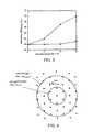
- FIG. 3is a graph of an extraction efficiency of an LED with a patterned surface as function of a detuning parameter.
- FIG. 4is a schematic representation of the Fourier transformation of a patterned surface of an LED.
- FIG. 5is a graph of an extraction efficiency of an LED with a patterned surface as function of nearest neighbor distance.
- FIG. 6is a graph of an extraction efficiency of an LED with a patterned surface as function of a filling factor.
- FIG. 7is a top view a patterned surface of an LED.
- FIG. 8is a graph of an extraction efficiency of LEDs with different surface patterns.
- FIG. 9is a graph of an extraction efficiency of LEDs with different surface patterns.
- FIG. 10is a graph of an extraction efficiency of LEDs with different surface patterns.
- FIG. 11is a graph of an extraction efficiency of LEDs with different surface patterns.
- FIG. 12is a schematic representation of the Fourier transformation two LEDs having different patterned surfaces compared with the radiation emission spectrum of the LEDs.
- FIG. 13is a graph of an extraction efficiency of LEDs having different surface patterns as a function of angle.
- FIG. 14is a side view of an LED with a patterned surface and a phosphor layer on the patterned surface.
- FIG. 15is a side view of a epitaxial layer precursor to an LED with a patterned surface.
- FIG. 16is a side view of a epitaxial layer precursor to an LED with a patterned surface.
- FIG. 17is a side view of a epitaxial layer precursor to an LED with a patterned surface.
- FIG. 18is a side view of a epitaxial layer precursor to an LED with a patterned surface.
- FIG. 19is a side view of a epitaxial layer precursor to an LED with a patterned surface.
- FIG. 1shows a side view of an LED 100 in the form of a packaged die.
- LED 100includes a multi-layer stack 122 disposed on a submount 120 .
- Multi-layer stack 122includes a 320 nm thick silicon doped (n-doped) GaN layer 134 having a pattern of openings 150 in its upper surface 110 .
- Multi-layer stack 122also includes a bonding layer 124 , a 100 nm thick silver layer 126 , a 40 nm thick magnesium doped (p-doped) GaN layer 128 , a 120 nm thick light-generating region 130 formed of multiple InGaN/GaN quantum wells, and a AlGaN layer 132 .
- An n-side contact pad 136is disposed on layer 134
- a p-side contact pad 138is disposed on layer 126 .
- An encapsulant material (epoxy having an index of refraction of 1.5) 144is present between layer 134 and a cover slip 140 and supports 142 . Layer 144 does not extend into openings 150 .
- Lightis generated by LED 100 as follows.
- P-side contact pad 138is held at a positive potential relative to n-side contact pad 136 , which causes electrical current to be injected into LED 100 .
- As the electrical current passes through light-generating region 130electrons from n-doped layer 134 combine in region 130 with holes from p-doped layer 128 , which causes region 130 to generate light.
- Light-generating region 130contains a multitude of point dipole radiation sources that emit light (e.g., isotropically) within the region 130 with a spectrum of wavelengths characteristic of the material from which light-generating region 130 is formed.
- the spectrum of wavelengths of light generated by region 130can have a peak wavelength of about 445 nanometers (nm) and a full width at half maximum (FWHM) of about 30 nm.
- the charge carriers in p-doped layer 126have relatively low mobility compared to the charge carriers in the n-doped semiconductor layer 134 .
- placing silver layer 126 (which is conductive) along the surface of p-doped layer 128can enhance the uniformity of charge injection from contact pad 138 into p-doped layer 128 and light-generating region 130 . This can also reduce the electrical resistance of device 100 and/or increase the injection efficiency of device 100 .
- Because of the relatively high charge carrier mobility of the n-doped layer 134electrons can spread relatively quickly from n-side contact pad 136 throughout layers 132 and 134 , so that the current density within the light-generating region 130 is substantially uniform across the region 130 .
- silver layer 126has relatively high thermal conductivity, allowing layer 126 to act as a heat sink for LED 100 (to transfer heat vertically from the multi-layer stack 122 to submount 120 ).
- At least some of the light that is generated by region 130is directed toward silver layer 126 .
- This lightcan be reflected by layer 126 and emerge from LED 100 via surface 110 , or can be reflected by layer 126 and then absorbed within the semiconductor material in LED 100 to produce an electron-hole pair that can combine in region 130 , causing region 130 to generate light.
- at least some of the light that is generated by region 130is directed toward pad 136 .
- the underside of pad 136is formed of a material (e.g., a Ti/Al/Ni/Au alloy) that can reflect at least some of the light generated by light-generating region 130 .
- the light that is directed to pad 136can be reflected by pad 136 and subsequently emerge from LED 100 via surface 110 (e.g., by being reflected from silver layer 126 ), or the light that is directed to pad 136 can be reflected by pad 136 and then absorbed within the semiconductor material in LED 100 to produce an electron-hole pair that can combine in region 130 , causing region 130 to generate light (e.g., with or without being reflected by silver layer 126 ).
- surface 110 of LED 100is not flat but consists of a modified triangular pattern of openings 150 .
- various valuescan be selected for the depth of openings 150 , the diameter of openings 150 and the spacing between nearest neighbors in openings 150 can vary.
- openings 150have a depth 146 equal to about 280 nm, a non-zero diameter of about 160 nm, a spacing between nearest neighbors or about 220 nm, and an index of refraction equal to 1.0.
- the triangular patternis detuned so that the nearest neighbors in pattern 150 have a center-to-center distance with a value between (a ⁇ a) and (a+ ⁇ a), where “a” is the lattice constant for an ideal triangular pattern and “ ⁇ a” is a detuning parameter with dimensions of length and where the detuning can occur in random directions.
- detuning parameter, ⁇ ais generally at least about one percent (e.g., at least about two percent, at least about three percent, at least about four percent, at least about five percent) of ideal lattice constant, a, and/or at most about 25% (e.g., at most about 20%, at most about 15%, at most about 10%) of ideal lattice constant, a.
- the nearest neighbor spacingsvary substantially randomly between (a ⁇ a) and (a+ ⁇ a), such that pattern 150 is substantially randomly detuned.
- the extraction efficiency data shown in FIG. 3are calculated by using a three-dimensional finite-difference time-domain (FDTD) method to approximate solutions to Maxwell's equations for the light within and outside of LED 100 .
- FDTDfinite-difference time-domain
- input parameters in a FDTD calculationinclude the center frequency and bandwidth of the light emitted by the point dipole radiation sources in light-generating region 130 , the dimensions and dielectric properties of the layers within multilayer stack 122 , and the diameters, depths, and nearest neighbor distances (NND) between openings in pattern 150 .
- extraction efficiency data for LED 100are calculated using an FDTD method as follows.
- the FDTD methodis used to solve the full-vector time-dependent Maxwell's equations:
- the individual ⁇ right arrow over (P) ⁇ m termsare empirically derived values of different contributions to the overall polarizability of a material (e.g., the polarization response for bound electron oscillations, the polarization response for free electron oscillations).
- a materiale.g., the polarization response for bound electron oscillations, the polarization response for free electron oscillations.
- ⁇ ⁇ ( ⁇ )⁇ ⁇ + ⁇ m ⁇ s m ⁇ m 2 - ⁇ 2 - i ⁇ m ⁇ ⁇ .
- the only layers that are consideredare encapsulant 144 , silver layer 126 and layers between encapsulant 144 and silver layer 126 . This approximation is based on the assumption that encapsulant 144 and layer 126 are thick enough so that surrounding layers do not influence the optical performance of LED 100 .
- the relevant structures within LED 100 that are assumed to have a frequency dependent dielectric constantare silver layer 126 and light-generating region 130 .
- the other relevant layers within LED 100are assumed to not have frequency dependent dielectric constants. It is to be noted that in embodiments in which LED 100 includes additional metal layers between encapsulant 144 and silver layer 126 , each of the additional metal layers will have a corresponding frequency dependent dielectric constant.
- silver layer 126(and any other metal layer in LED 100 ) has a frequency dependent term for both bound electrons and free electrons, whereas light-generating region 130 has a frequency dependent term for bound electrons but does not have a frequency dependent term for free electrons.
- other termscan be included when modeling the frequency dependence of the dielectric constant. Such terms may include, for example, electron-phonon interactions, atomic polarizations, ionic polarizations and/or molecular polarizations.
- the emission of light from the quantum well region of light-generating region 130is modeled by incorporating a number of randomly-placed, constant-current dipole sources within the light-generating region 130 , each emitting short Gaussian pulses of spectral width equal to that of the actual quantum well, each with random initial phase and start-time.
- a large supercell in the lateral directionis used, along with periodic boundary conditions. This can assist in simulating relatively large (e.g., greater than 0.01 mm on edge) device sizes.
- the full evolution equationsare solved in time, long after all dipole sources have emitted their energy, until no energy remains in the system.
- the total energy emitted, the energy flux extracted through top surface 110 , and the energy absorbed by the quantum wells and the n-doped layeris monitored. Through Fourier transforms both in time and space, frequency and angle resolved data of the extracted flux are obtained, and therefore an angle- and frequency-resolved extraction efficiency can be calculated.
- absolute angle-resolved extraction in lumens/per solid angle/per chip area for given electrical inputis obtained.
- the detuned pattern 150can enhance the efficiency with which light generated in region 130 emerges from LED 100 via surface 110 because openings 150 create a dielectric function that varies spatially in layer 134 according to pattern 150 . It is believed that this alters the density of radiation modes (i.e., light modes that emerge from surface 110 ) and guided modes (i.e., light modes that are confined within multi-layer stack 122 ) within LED 100 , and that this alteration to the density of radiation modes and guided modes within LED 100 results in some light that would otherwise be emitted into guided modes in the absence of pattern 150 being scattered (e.g., Bragg scattered) into modes that can leak into radiation modes. In certain embodiments, it is believed that pattern 150 (e.g., the pattern discussed above, or one of the patterns discussed below) can eliminate all of the guided modes within LED 100 .
- pattern 150e.g., the pattern discussed above, or one of the patterns discussed below
- the effect of detuning of the latticecan be understood by considering Bragg scattering off of a crystal having point scattering sites.
- the Bragg conditioncan be relaxed by detuning the spacing of between lattice sites by a detuning parameter ⁇ a. It is believed that detuning the lattice increases the scattering effectiveness and angular acceptance of the pattern over the spectral bandwidth and spatial emission profile of the source.
- modified triangular pattern 150 having a non-zero detuning parameter ⁇ ahas been described that can enhance light extraction from LED 100
- other patternscan also be used to enhance light extraction from LED 100 .
- physical insightmay first be used to approximate a basic pattern that can enhance light extraction before conducting such numerical calculations.
- the extraction efficiency of LED 100can be further understood (e.g., in the weak scattering regime) by considering the Fourier transform of the dielectric function that varies spatially according to pattern 150 .
- the extraction efficiencyis proportional to the magnitude of the corresponding Fourier component (F k ) of the dielectric function ⁇ G given by
- the maximum G to be consideredis fixed by the frequency ( ⁇ ) emitted by the light-generating region and the dielectric constant of the light-generating region. As shown in FIG. 4 , this defines a ring in reciprocal space which is often called the light line.
- the light linewill be an annulus due to the finite bandwidth of the light-generating region but for sake of clarity we illustrate the light line of a monochromatic source.
- light propagating within the encapsulantis bounded by a light line (the inner circle in FIG. 4 ).
- the extraction efficiencyis improved by increasing F k for all directions k that lie within the encapsulant light-line which amounts to increasing the number of G points within the encapsulant light line and increasing the scattering strength ⁇ G for G points which lie within the material light line. This physical insight can be used when selecting patterns that can improve extraction efficiency.
- FIG. 5shows the effect of increasing lattice constant for an ideal triangular pattern.
- the data shown in FIG. 5are calculated using the parameters given for LED 100 shown in FIG. 1 , except that the emitted light has a peak wavelength of 450 nm, and the depth of the holes, the diameter of the holes, and the thickness of the n-doped layer 134 scale with the nearest neighbor distance, a, as 1.27 a, 0.72 a, and 1.27 a+40 nm, respectively.
- Increasing the lattice constantincreases the density of G points within the light-line of the encapsulant.
- a clear trend in extraction efficiency with NNDis observed. It is believed that the maximum extraction efficiency occurs for NND approximately equal to the wavelength of light in vacuum. The reason a maximum is achieved, is that as the NND becomes much larger than the wavelength of light, the scattering effect is reduced because the material becomes more uniform.
- FIG. 6shows the effect of increasing hole size or filling factor.
- the filling factor for a triangular patternis given by (2 ⁇ / ⁇ 3)*(r/a) 2 , where r is the radius of a hole.
- the data shown in FIG. 6are calculated using the parameters given for the LED 100 shown in FIG. 1 , except that the diameter of the openings is changed according the filling factor value given on the x-axis of the graph.
- the extraction efficiencyincreases with filling factor as the scattering strengths ( ⁇ G ) increase. A maximum is observed for this particular system at a filling factor of ⁇ 48%.
- LED 100has a filling factor of at least about 10% (e.g., at least about 15%, at least about 20%) and/or at most about 90% (e.g., at most about 80%, at most about 70%, at most about 60%).
- a modified (detuned) triangular patternmay also be achieved by modifying the holes in an ideal triangular pattern while keeping the centers at the positions for an ideal triangular pattern.
- FIG. 7shows an embodiment of such a pattern.
- the enhancement in light extraction, the methodology for conducting the corresponding numerical calculation, and the physical explanation of the enhanced light extraction for a light-emitting device having the pattern shown in FIG. 7is generally the same as described above.
- a modified (detuned) patterncan have openings that are displaced from the ideal locations and openings at the ideal locations but with varying diameters.
- enhanced light extraction from a light-emitting devicecan be achieved by using different types of patterns, including, for example, complex periodic patterns and nonperiodic patterns.
- a complex periodic patternis a pattern that has more than one feature in each unit cell that repeats in a periodic fashion.
- Examples of complex periodic patternsinclude honeycomb patterns, honeycomb base patterns, (2 ⁇ 2) base patterns, ring patterns, and Archimidean patterns.
- a complex periodic patterncan have certain openings with one diameter and other openings with a smaller diameter.
- a nonperiodic patternis a pattern that has no translational symmetry over a unit cell that has a length that is at least 50 times the peak wavelength of light generated by region 130 .
- Examples of nonperiodic patternsinclude aperiodic patterns, quasicrystalline patterns, Robinson patterns, and Amman patterns.
- FIG. 8shows numerical calculations for LED 100 for two different complex periodic patterns in which certain openings in the patterns have a particular diameter, and other openings in the patterns have smaller diameters.
- the numerical calculations represented in FIG. 8show the behavior of the extraction efficiency (larger holes with a diameter of 80 nm) as the diameter of the smaller holes (dR) is varied from zero nm to 95 nm.
- the data shown in FIG. 6are calculated using the parameters given for the LED 100 shown in FIG. 1 , except that the diameter of the openings is changed according the filling factor value given on the x-axis of the graph.
- multiple hole sizesallow scattering from multiple periodicities within the pattern, therefore increasing the angular acceptance and spectral effectiveness of the pattern.
- the enhancement in light extraction, the methodology for conducting the corresponding numerical calculation, and the physical explanation of the enhanced light extraction for a light-emitting device having the pattern shown in FIG. 8is generally the same as described above.
- FIG. 9shows numerical calculations for LED 100 having different ring patterns (complex periodic patterns).
- the number of holes in the first ring surrounding the central holeis different (six, eight or 10) for the different ring patterns.
- the data shown in FIG. 9are calculated using the parameters given for the LED 100 shown in FIG. 1 , except that the emitted light has a peak wavelength of 450 nm.
- the numerical calculations represented in FIG. 9show the extraction efficiency of LED 100 as the number of ring patterns per unit cell that is repeated across a unit cell is varied from two to four.
- the enhancement in light extraction, the methodology for conducting the corresponding numerical calculation, and the physical explanation of the enhanced light extraction for a light-emitting device having the pattern shown in FIG. 9is generally the same as described above.
- FIG. 10shows numerical calculations for LED 100 having an Archimidean pattern.
- the Archimidean tiling A19consists of 19 equally-spaced holes with a NND of a.
- the holesare arranged in the form of an inner hexagon of seven holes, and outer hexagon of 12 holes, and a central hole within the inner hexagon.
- the enhancement in light extraction, the methodology for conducting the corresponding numerical calculation, and the physical explanation of the enhanced light extraction for a light-emitting device having the pattern shown in FIG. 10is generally the same as described above. As shown in FIG. 10 the extraction efficiency for A7 and A19 is about 77%.
- the data shown in FIG. 10are calculated using the parameters given for the LED 100 shown in FIG. 1 , except that the emitted light has a peak wavelength of 450 and except that the NND is defined as the distance between openings within an individual cell.
- FIG. 11shows numerical calculation data for LED 100 having a quasicrystalline pattern.
- Quasicrystalline patternsare described, for example, in M. Senechal, Quasicrystals and Geometry (Cambridge University Press, Cambridge, England 1996), which is hereby incorporated by reference.
- the numerical calculationsshow the behavior of the extraction efficiency as the class of 8-fold based quasi-periodic structure is varied. It is believed that quasicrystalline patterns exhibit high extraction efficiency due to high degree of in-plane rotational symmetries allowed by such structures.
- the enhancement in light extraction, the methodology for conducting the corresponding numerical calculation, and the physical explanation of the enhanced light extraction for a light-emitting device having the pattern shown in FIG. 11is generally the same as described above. Results from FDTD calculations shown in FIG.
- FIG. 11indicate that the extraction efficiency of quasicrystalline structures reaches about 82%.
- the data shown in FIG. 11are calculated using the parameters given for the LED 100 shown in FIG. 1 , except that the emitted light has a peak wavelength of 450 and except that the NND is defined as the distance between openings within an individual cell.
- At least about 45%e.g., at least about 50%, at least about 55%, at least about 60%, at least about 70%, at least about 80%, at least about 90%, at least about 95%) of the total amount of light generated by light-generating region 130 that emerges from LED 100 emerges via surface 110 .
- the cross-sectional area of LED 100can be relatively large, while still exhibiting efficient light extraction from LED 100 .
- one or more edges of LED 100can be at least about one millimeter (e.g., at least about 1.5 millimeters, at least about two millimeters, at least about 2.5 millimeters, at least about three millimeters), and at least about 45% (e.g., at least about 50%, at least about 55%, at least about 60%, at least about 70%, at least about 80%, at least about 90%, at least about 95%) of the total amount of light generated by light-generating region 130 that emerges from LED 100 emerges via surface 110 .
- Thiscan allow for an LED to have a relatively large cross-section (e.g., at least about one millimeter by at least about one millimeter) while exhibiting good power conversion efficiency.
- the extraction efficiency of an LED having the design of LED 100is substantially independent of the length of the edge of the LED.
- the difference between the extraction efficiency of an LED having the design of LED 100 and one or more edges having a length of about 0.25 millimeter and the extraction efficiency of LED having the design of LED 100 and one or more edges having a length of one millimetercan vary by less than about 10% (e.g., less than about 8%, less than about 5%, less than about 3%).
- the extraction efficiency of an LEDis the ratio of the light emitted by the LED to the amount of light generated by the device (which can be measured in terms of energy or photons). This can allow for an LED to have a relatively large cross-section (e.g., at least about one millimeter by at least about one millimeter) while exhibiting good power conversion efficiency.
- the quantum efficiency of an LED having the design of LED 100is substantially independent of the length of the edge of the LED.
- the difference between the quantum efficiency of an LED having the design of LED 100 and one or more edges having a length of about 0.25 millimeter and the quantum efficiency of LED having the design of LED 100 and one or more edges having a length of one millimetercan vary by less than about 10% (e.g., less than about 8%, less than about 5%, less than about 3%).
- the quantum efficiency of an LEDis the ratio of the number of photons generated by the LED to the number of electron-hole recombinations that occur in the LED. This can allow for an LED to have a relatively large cross-section (e.g., at least about one millimeter by at least about one millimeter) while exhibiting good performance.
- the wall plug efficiency of an LED having the design of LED 100is substantially independent of the length of the edge of the LED.
- the difference between the wall plug efficiency of an LED having the design of LED 100 and one or more edges having a length of about 0.25 millimeter and the wall plug efficiency of LED having the design of LED 100 and one or more edges having a length of one millimetercan vary by less than about 10% (e.g., less than about 8%, less than about 5%, less than about 3%).
- the wall plug efficiency of an LEDis the product of the injection efficiency of the LED (the ratio of the numbers of carriers injected into the device to the number of carriers that recombine in the light-generating region of the device), the radiative efficiency of the LED (the ratio of electron-hole recombinations that result in a radiative event to the total number of electron-hole recombinations), and the extraction efficiency of the LED (the ratio of photons that are extracted from the LED to the total number of photons created).
- Thiscan allow for an LED to have a relatively large cross-section (e.g., at least about one millimeter by at least about one millimeter) while exhibiting good performance.
- a given solid anglee.g., into a solid angle around the direction normal to surface 110
- FIG. 12shows the Fourier transform construction for two ideal triangular lattices of different lattice constant.
- ⁇ Gscattering strengths of G points
- FIG. 13which shows extraction efficiency into a solid angle (given by the collection half-angle in the diagram).
- the data shown in FIG. 13are calculated using the parameters given for the LED 100 shown in FIG. 1 , except that the emitted light has a peak wavelength of 530 nm and a bandwidth of 34 nm, the index of refraction of the encapsulant was 1.0, the thickness of the p-doped layer was 160 nm, the light generating layer was 30 nm thick, the NND (a) for the three curves is shown on FIG. 13 , and the depth, hole diameter, and n-doped layer thickness scaled with a, as 1.27 a, 0.72 a, and 1.27 a+40 nm, respectively.
- the approachis especially applicable for reducing the source etendue which is believed to often be proportional to n 2 , where n is the index of refraction of the surrounding material (e.g., the encapsulant). It is therefore believed that reducing the index of refraction of the encapsulating layer for LED 100 can lead to more collimated emission, a lower source etendue, and therefore to a higher surface brightness (here defined as the total lumens extracted into the etendue of the source). In some embodiments then, using an encapsulant of air will reduce the source etendue while increasing extraction efficiency into a given collection angle centered around the normal direction.
- the distribution of lightis more collimated than a lambertian distribution.
- at least about 40%e.g., at least about 50%, at least about 70%, at least about 90%
- the light emerging via the surface of the dielectric layeremerges within at most about 30° (e.g., at most about 25°, at most about 20°, at most about 15°) of an angle normal to surface 110 .
- a waferhas at least about five LEDs (e.g., at least about 25 LEDs, at least about 50 LEDs) per square centimeter.
- an LED 300 having a layer containing a phosphor material 180can be disposed on surface 110 .
- the phosphor materialcan interact with light at the wavelength(s) generated by region 130 to provide light at desired wavelength(s).
- the phosphor material in layer 180can be formed of, for example, a (Y,Gd)(Al,Ga)G:Ce 3+ or “YAG” (yttrium, aluminum, garnet) phosphor.
- the phosphor material in layer 180can be activated and emit light (e.g., isotropically) with a broad spectrum centered around yellow wavelengths.
- a viewer of the total light spectrum emerging from packaged LED 100sees the yellow phosphor broad emission spectrum and the blue InGaN narrow emission spectrum and typically mixes the two spectra to perceive white.
- layer 180can be substantially uniformly disposed on surface 110 .
- the distance between the top 151 of pattern 150 and the top 181 of layer 180can vary by less than about 20% (e.g., less than about 10%, less than about 5%, less than about 2%) across surface 110 .
- the thickness of layer 180is small compared to the cross-sectional dimensions of surface 130 of LED 100 , which are typically about one millimeter (mm) by one mm. Because layer 180 is substantially uniformly deposited on surface 110 , the phosphor material in layer 180 can be substantially uniformly pumped by light emerging via surface 110 .
- the phosphor layer 180is relatively thin compared to the dimensions of the surface 110 of the LED 100 , such that light emitted by the light-generating region 130 is converted into lower wavelength light within the phosphor layer 180 approximately uniformly over the entire surface 110 of LED 100 .
- the relatively thin, uniform phosphor layer 180produces a uniform spectrum of white light emitted from the LED 100 as a function of position on surface 110 .
- LED 100can be fabricated as desired. Typically, fabrication of LED 100 involves various deposition, laser processing, lithography, and etching steps.
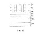
- a LED wafer 500 containing an LED layer stack of material deposited on a sapphire substrateis readily available and can be purchased from a commercial vendor.
- a buffer layer 504On the sapphire substrate 502 are disposed, consecutively, a buffer layer 504 , an n-doped Si:GaN layer 506 , an AlGaN/GaN heterojunction or superlattice that provides a current spreading layer 508 , an InGaN/GaN multi-quantum well light-generating region 510 , and a p-doped Mg:GaN layer 512 .
- the commercially available LED waferis about 2-3 inches in diameter and multiple LED dice can be cut from the wafer to form individual devices after the wafer has been processed. Before dicing the wafer, a number of wafer scale processing steps are used to position the p-doped layer 128 on the same side of the light-generating region 130 as the mirror layer 126 .
- a relatively thin nickel layer 520is deposited (e.g., using electron-beam evaporation) on p-doped layer 512 to form a p-type ohmic contact to p-doped layer 512 .
- a silver layer 522is deposited (e.g., using electron-beam evaporation) on nickel layer 520 .
- a relatively thick nickel layer 524is deposited on silver layer 522 (e.g., using electron-beam evaporation). Layer 524 can act as diffusion barrier to reduce the diffusion of contaminants into silver layer 522 .
- a gold layer 526is deposited on nickel layer 524 (e.g., using resistance evaporation). Wafer 500 is then annealed at a temperature between 400 and 600 degrees Celsius for between 30 and 300 seconds in a nitrogen, oxygen, air, or forming gas to achieve an ohmic contact.
- a submount wafer 600is prepared by depositing on a p-doped silicon wafer 602 , consecutively (e.g., using electron-beam evaporation) an aluminum contact layer 604 .
- a gold layer 608is deposited (e.g., using thermal evaporation) onto layer 604
- a AuSn bonding layer 610is deposited (e.g., using thermal evaporation) onto layer 608 .
- Submount wafer 600is annealed at a temperature between 350 and 500 degrees Celsius for between 30 and 300 seconds in a nitrogen, oxygen, air, or forming gas to achieve an ohmic contact.
- Wafer 500 and 600are bonded together by bringing the layer 526 into contact with layer 610 of the submount wafer 600 (e.g., using a thermal-mechanical press) using pressures from 0 to 0.5 MPa and temperatures ranging from 200-400 degrees Celsius. Layer 510 and layer 610 form a eutectic bond. The combined wafer sandwich is cooled and the bonded sandwich is removed from the press.
- substrate 502is removed from the combined structure by a laser liftoff process.
- Laser liftoff processesare disclosed, for example, in U.S. Pat. Nos. 6,420,242 and 6,071,795, which are hereby incorporated by reference.
- a 248 nm laser beamis shined through substrate 502 to locally heat n-doped Si:GaN layer 506 near its interface with sapphire substrate 502 , decomposing a sublayer of n-doped layer 506 .
- the wafer sandwichis then heated to above the melting point of gallium, at which point sapphire substrate 502 is removed from the sandwich by applying a lateral force to it (e.g., using a cotton swab).
- the exposed GaN surfaceis then cleaned (e.g., using a hydrochloric acid bath) to remove liquid gallium from the surface.
- sapphire substrate 502is removed from the GaN epitaxial layer stack
- strain that was present in the stacke.g., due to the lattice mismatch between substrate 502 and the stack
- the coefficient of thermal expansionis considered when choosing the submount to avoid cracking in the laser liftoff process.
- crackingcan be reduced during laser-liftoff by substantially overlapping fields in the step and repeat process.
- the exposed surface of n-doped Si:GaN layer 506is etched back (e.g., using a reactive ion etching process) to achieve a desired thickness for the layer to be used in the final device ( FIG. 19 ).
- the surface of the etched GaN layer 506has a roughened surface texture 700 due to the etching.
- Roughened surface 700can be planarized and thinned (e.g., using a chemical-mechanical process) to achieve a final thickness for layer 506 and surface smoothness of less than about 5 nm root mean square (rms).
- roughened surface 700can be maintained in order to aid in increasing the extraction efficiency of the device by introducing a locally non-planar interface to the device 100 .
- the roughened surfaceincreases the probability, with respect to a microscopically smooth surface, that a light ray that strikes surface 700 multiple times will eventually strike the surface at an angle that less than the critical angle given by Snell's law and will be extracted through the surface 700 .
- a planarization layer 702 of a materiale.g., a polymer
- a resist layer 704is disposed (e.g., spin-coated) onto planarization layer 702 .
- the pattern that forms the photonic lattice in the LEDis then created in n-doped layer 506 by a nanoimprint lithography and etching process.
- a mold that defines a portion of the desired patternis pressed into the resist layer 704 and stepped across the entire surface of the wafer in a portion-by-portion manner to print the features of the pattern 150 and leaving regions for depositing n-contacts later on in the process flow.
- the surface of n-doped layer 506is substantially flat during this portion of the process.
- X-ray lithography or deep ultraviolet lithography, for example,can also be used to create the pattern in resist layer 704 .
- a predeposited etch maskcan be laid down on the surface of layer 506 .
- Patterned layer 704is used as a mask to transfer the pattern into the planarization layer 702 (e.g., using a reactive-ion etching process). Planarization layer is subsequently used as a mask to transfer the pattern into the n-doped layer 506 . Following etching of GaN layer 506 , the planarization layer is removed (e.g., using an oxygen-based reactive ion etch).
- a layer of phosphor materialcan optionally be disposed (e.g., spin-coated) onto the patterned surface of n-doped layer 506 .
- the phosphorcan conformally coat the patterned surface (coat with substantially no voids present along the bottoms and sidewalls of the openings in the patterned surface).
- a layer of encapsulant materialcan be disposed on the surface of patterned n-doped layer 506 (e.g. by CVD, sputtering, suspension by liquid binder that is subsequently evaporated).
- the encapsulantcan contain one or more phosphor materials.
- the phosphorcan be compressed to achieve thickness uniformity less that 20%, less than 15%, less than 10%, less than 5%, or less than 2% of the average thickness of the phosphor.
- the phosphor-containing encapsulantcan conformally coat the patterned surface.
- individual LED dicecan be cut from the wafer. Once wafer processing and wafer testing is complete, individual LED dice are separated and prepared for packaging and testing. A sidewall passivation step and/or a pre-separation deep mesa etching step may be used to reduce potential damage to the electrical and/or optical properties of the patterned LED incurred during wafer cutting.
- the individual LEDscan be any size up to the size of the wafer itself, but individual LEDs are typically square or rectangular, with sides having a length between about 0.5 mm to 5 mm.
- standard photolithographyis used to define the location of contact pads on the wafer for energizing the device, and ohmic contacts are evaporated (e.g. using electron beam evaporation) onto the desired locations.
- the packageshould generally be capable of facilitating light collection while also providing mechanical and environmental protection of the die.
- a transparent covercan be packaged on the LED die to protect the patterned surface of the 506 when an encapsulant is not used.
- the cover slipis attached to supports 142 using a glassy frit that is melted in a furnace.
- the opposite ends of the supportsare connected using a cap weld or an epoxy for example.
- Supportsare typically Ni-plated to facilitate welding to an Au plated surface of the package. It believed that the absence of an encapsulant layer allows higher tolerable power loads per unit area in the patterned surface LED 100 . Degradation of the encapsulant can be a common failure mechanism for standard LEDs and is avoided not using an encapsulant layer.
- the LEDsare cut from a large area flat wafer, their light output per area does not decrease with area. Also, because the cross section of an individual LEDs cut from a wafer is only slightly larger than the light-emitting surface area of the LED, many individual, and separately addressable LEDs can be packed closely together in an array. If one LED does not function (e.g., due to a large defect), then it does not significant diminish the performance of the array because the individual devices are closely packed.
- the light-emitting devicecan have any desired thickness, and the individual layers within the light-emitting device can have any desired thickness.
- the thicknesses of the layers within multi-layer stack 122are chosen so as to increase the spatial overlap of the optical modes with light-generating region 130 , to increase the output from light generated in region 130 .
- Exemplary thicknesses for certain layers in a light-emitting deviceinclude the following.
- layer 134can have a thickness of at least about 100 nm (e.g., at least about 200 nm, at least about 300 nm, at least about 400 nm, at least about 500 nm) and/or at most about 10 microns (e.g., at most about five microns, at most about three microns, at most about one micron).
- layer 128has a thickness of at least about 10 nm (e.g., at least about 25 nm, at least about 40 nm) and/or at most about one micron (e.g., at most about 500 nm, at most about 100 nm).
- layer 126has a thickness of at least about 10 nm (e.g., at least about 50 nm, at least about 100 nm) and/or at most about one micron (e.g., at most about 500 nm, at most about 250 nm).
- light-generating region 130has a thickness of at least about 10 nm (e.g., at least about 25 nm, at least about 50 nm, at least about 100 nm) and/or at most about 500 nm (e.g., at most about 250 nm, at most about 150 nm).
- light-emitting diodeAs an example, while a light-emitting diode has been described, other light-emitting devices having the above-described features (e.g., patterns, processes) can be used. Such light-emitting devices include lasers and optical amplifiers.
- a current spreading layercan be integral with (e.g., a portion of) layer 134 .
- the current spreading layercan be a relatively highly n-doped portion of layer 134 or a heterojunction between (e.g. AlGaN/GaN) to form a 2D electron gas.
- any semiconductor materialse.g., III-V semiconductor materials, organic semiconductor materials, silicon
- any semiconductor materialscan be used that can be used in a light-emitting device.
- Examples of other light-generating materialsinclude InGaAsP, AlInGaN, AlGaAs, InGaAlP.
- Organic light-emitting materialsinclude small molecules such as aluminum tris-8-hydroxyquinoline (Alq 3 ) and conjugated polymers such as poly[2-methoxy-5-(2-ethylhexyloxy)-1,4-vinylenephenylene] or MEH-PPV.
- the LEDscan also be small area LEDs (e.g., LEDs smaller than the standard about 300 microns on edge).
- a dielectric function that varies spatially according to a patternhas been described in which the pattern is formed of holes, the pattern can also be formed in other ways.
- a patterncan be formed continuous veins and/or discontinuous veins in the appropriate layer.
- the pattern in varying dielectric functioncan be achieved without using holes or veins.
- materials having different dielectric functionscan be patterned in the appropriate layer. Combinations of such patterns can also be used.
- layer 126has been described as being formed of silver, other materials can also be used.
- layer 126is formed of a material that can reflect at least about 50% of light generated by the light-generating region that impinges on the layer of reflective material, the layer of reflective material being between the support and the multi-layer stack of materials. Examples of such materials include distributed Bragg reflector stacks and various metals and alloys, such as aluminum and aluminum-containing alloys.
- support 120can be formed of a variety of materials. Examples of materials from which support 120 can be formed include copper, copper-tungsten, aluminum nitride, silicon carbide, beryllium-oxide, diamonds, TEC and aluminum.
- a light-emitting devicecan include a separate layer (e.g., disposed between layer 126 and submount 120 ) that serves as a heat sink.
- layer 126may or may not be formed of a material that can serve as a heat sink.
- the varying pattern in dielectric functionhas been described as extending into n-doped layer 134 only (which can substantially reduce the likelihood of surface recombination carrier losses) in addition to making use of the entire light-generating region, in some embodiments, the varying pattern in dielectric function can extend beyond n-doped layer (e.g., into current spreading layer 132 , light-generating region 130 , and/or p-doped layer 128 ).
- aircan be disposed between surface 110 can cover slip 140
- materials other than, or in an addition to, aircan be disposed between surface 110 and cover slip 140 .
- such materialshave an index of refraction of at least about one and less than about 1.5 (e.g., less than about 1.4, less than about 1.3, less than about 1.2, less than about 1.1).
- examples of such materialsinclude nitrogen, air, or some higher thermal conductivity gas.
- surface 110may or may not be patterned.
- surface 110may be non-patterned but may be roughened (i.e., having randomly distributed features of various sizes and shapes less than ⁇ /5).
- a light-emitting devicecan include a layer of a phosphor material coated on surface 110 , cover layer 140 and supports 142 .
- a light-emitting devicecan include a cover layer 140 that has a phosphor material disposed therein.
- surface 110may or may not be patterned.
- the light emitted by the light-generating region 130is UV (or violet, or blue) and the phosphor layer 180 includes a mixture of a red phosphor material (e.g., L 2 O 2 S:Eu 3+ ), a green phosphor material (e.g, ZnS:Cu, Al, Mn), and blue phosphor material (e.g, (Sr, Ca, Ba, Mg) 10 (PO 4 ) 6 Cl:Eu 2+ ).
- a red phosphor materiale.g., L 2 O 2 S:Eu 3+
- a green phosphor materiale.g, ZnS:Cu, Al, Mn
- blue phosphor materiale.g, (Sr, Ca, Ba, Mg) 10 (PO 4 ) 6 Cl:Eu 2+
Landscapes
- Led Devices (AREA)
- Led Device Packages (AREA)
- Electroluminescent Light Sources (AREA)
- Semiconductor Lasers (AREA)
Abstract
Description
where the polarizability {right arrow over (P)}={right arrow over (P)}1+{right arrow over (P)}2+ . . . +{right arrow over (P)}mcaptures the frequency-dependent response of the quantum well light-generating
where the polarization corresponds to a dielectric constant
Claims (12)
Priority Applications (2)
| Application Number | Priority Date | Filing Date | Title |
|---|---|---|---|
| US12/248,870US7994521B2 (en) | 2003-04-15 | 2008-10-09 | Light emitting devices |
| US13/170,777US8513692B2 (en) | 2003-04-15 | 2011-06-28 | Light emitting devices |
Applications Claiming Priority (14)
| Application Number | Priority Date | Filing Date | Title |
|---|---|---|---|
| US46288903P | 2003-04-15 | 2003-04-15 | |
| US47419903P | 2003-05-29 | 2003-05-29 | |
| US47568203P | 2003-06-04 | 2003-06-04 | |
| US50366103P | 2003-09-17 | 2003-09-17 | |
| US50367103P | 2003-09-17 | 2003-09-17 | |
| US50365303P | 2003-09-17 | 2003-09-17 | |
| US50365403P | 2003-09-17 | 2003-09-17 | |
| US50367203P | 2003-09-17 | 2003-09-17 | |
| US51380703P | 2003-10-23 | 2003-10-23 | |
| US51476403P | 2003-10-27 | 2003-10-27 | |
| US10/724,004US6831302B2 (en) | 2003-04-15 | 2003-11-26 | Light emitting devices with improved extraction efficiency |
| US10/993,342US7166870B2 (en) | 2003-04-15 | 2004-11-19 | Light emitting devices with improved extraction efficiency |
| US11/409,510US7719019B2 (en) | 2003-04-15 | 2006-04-22 | Light emitting devices |
| US12/248,870US7994521B2 (en) | 2003-04-15 | 2008-10-09 | Light emitting devices |
Related Parent Applications (1)
| Application Number | Title | Priority Date | Filing Date |
|---|---|---|---|
| US11/409,510ContinuationUS7719019B2 (en) | 2003-04-15 | 2006-04-22 | Light emitting devices |
Related Child Applications (1)
| Application Number | Title | Priority Date | Filing Date |
|---|---|---|---|
| US13/170,777ContinuationUS8513692B2 (en) | 2003-04-15 | 2011-06-28 | Light emitting devices |
Publications (2)
| Publication Number | Publication Date |
|---|---|
| US20090121243A1 US20090121243A1 (en) | 2009-05-14 |
| US7994521B2true US7994521B2 (en) | 2011-08-09 |
Family
ID=33163345
Family Applications (9)
| Application Number | Title | Priority Date | Filing Date |
|---|---|---|---|
| US10/724,004Expired - LifetimeUS6831302B2 (en) | 2003-04-15 | 2003-11-26 | Light emitting devices with improved extraction efficiency |
| US10/993,342Expired - LifetimeUS7166870B2 (en) | 2003-04-15 | 2004-11-19 | Light emitting devices with improved extraction efficiency |
| US11/409,510Active2026-03-06US7719019B2 (en) | 2003-04-15 | 2006-04-22 | Light emitting devices |
| US11/521,571Expired - LifetimeUS7495260B2 (en) | 2003-04-15 | 2006-09-14 | Light emitting devices |
| US11/879,035Expired - Fee RelatedUS7504669B2 (en) | 2003-04-15 | 2007-07-13 | Light emitting devices |
| US11/881,446AbandonedUS20080067525A1 (en) | 2003-04-15 | 2007-07-27 | Light emitting devices |
| US12/248,870Expired - Fee RelatedUS7994521B2 (en) | 2003-04-15 | 2008-10-09 | Light emitting devices |
| US12/370,074AbandonedUS20090206355A1 (en) | 2003-04-15 | 2009-02-12 | Light emitting devices |
| US13/170,777Expired - Fee RelatedUS8513692B2 (en) | 2003-04-15 | 2011-06-28 | Light emitting devices |
Family Applications Before (6)
| Application Number | Title | Priority Date | Filing Date |
|---|---|---|---|
| US10/724,004Expired - LifetimeUS6831302B2 (en) | 2003-04-15 | 2003-11-26 | Light emitting devices with improved extraction efficiency |
| US10/993,342Expired - LifetimeUS7166870B2 (en) | 2003-04-15 | 2004-11-19 | Light emitting devices with improved extraction efficiency |
| US11/409,510Active2026-03-06US7719019B2 (en) | 2003-04-15 | 2006-04-22 | Light emitting devices |
| US11/521,571Expired - LifetimeUS7495260B2 (en) | 2003-04-15 | 2006-09-14 | Light emitting devices |
| US11/879,035Expired - Fee RelatedUS7504669B2 (en) | 2003-04-15 | 2007-07-13 | Light emitting devices |
| US11/881,446AbandonedUS20080067525A1 (en) | 2003-04-15 | 2007-07-27 | Light emitting devices |
Family Applications After (2)
| Application Number | Title | Priority Date | Filing Date |
|---|---|---|---|
| US12/370,074AbandonedUS20090206355A1 (en) | 2003-04-15 | 2009-02-12 | Light emitting devices |
| US13/170,777Expired - Fee RelatedUS8513692B2 (en) | 2003-04-15 | 2011-06-28 | Light emitting devices |
Country Status (6)
| Country | Link |
|---|---|
| US (9) | US6831302B2 (en) |
| EP (1) | EP1614160A4 (en) |
| JP (2) | JP2007525817A (en) |
| KR (1) | KR100892957B1 (en) |
| TW (1) | TWI332715B (en) |
| WO (1) | WO2004093143A2 (en) |
Cited By (1)
| Publication number | Priority date | Publication date | Assignee | Title |
|---|---|---|---|---|
| US8513692B2 (en) | 2003-04-15 | 2013-08-20 | Luminus Devices, Inc. | Light emitting devices |
Families Citing this family (199)
| Publication number | Priority date | Publication date | Assignee | Title |
|---|---|---|---|---|
| US7211833B2 (en) | 2001-07-23 | 2007-05-01 | Cree, Inc. | Light emitting diodes including barrier layers/sublayers |
| US20060005763A1 (en) | 2001-12-24 | 2006-01-12 | Crystal Is, Inc. | Method and apparatus for producing large, single-crystals of aluminum nitride |
| US8545629B2 (en) | 2001-12-24 | 2013-10-01 | Crystal Is, Inc. | Method and apparatus for producing large, single-crystals of aluminum nitride |
| US7638346B2 (en) | 2001-12-24 | 2009-12-29 | Crystal Is, Inc. | Nitride semiconductor heterostructures and related methods |
| KR101030068B1 (en)* | 2002-07-08 | 2011-04-19 | 니치아 카가쿠 고교 가부시키가이샤 | Nitride semiconductor device manufacturing method and nitride semiconductor device |
| US7667238B2 (en) | 2003-04-15 | 2010-02-23 | Luminus Devices, Inc. | Light emitting devices for liquid crystal displays |
| US7274043B2 (en) | 2003-04-15 | 2007-09-25 | Luminus Devices, Inc. | Light emitting diode systems |
| US7262550B2 (en)* | 2003-04-15 | 2007-08-28 | Luminus Devices, Inc. | Light emitting diode utilizing a physical pattern |
| US7083993B2 (en) | 2003-04-15 | 2006-08-01 | Luminus Devices, Inc. | Methods of making multi-layer light emitting devices |
| US7105861B2 (en) | 2003-04-15 | 2006-09-12 | Luminus Devices, Inc. | Electronic device contact structures |
| US7166871B2 (en)* | 2003-04-15 | 2007-01-23 | Luminus Devices, Inc. | Light emitting systems |
| US7098589B2 (en) | 2003-04-15 | 2006-08-29 | Luminus Devices, Inc. | Light emitting devices with high light collimation |
| US7211831B2 (en)* | 2003-04-15 | 2007-05-01 | Luminus Devices, Inc. | Light emitting device with patterned surfaces |
| US20040259279A1 (en)* | 2003-04-15 | 2004-12-23 | Erchak Alexei A. | Light emitting device methods |
| US7521854B2 (en) | 2003-04-15 | 2009-04-21 | Luminus Devices, Inc. | Patterned light emitting devices and extraction efficiencies related to the same |
| US7084434B2 (en)* | 2003-04-15 | 2006-08-01 | Luminus Devices, Inc. | Uniform color phosphor-coated light-emitting diode |
| US7074631B2 (en) | 2003-04-15 | 2006-07-11 | Luminus Devices, Inc. | Light emitting device methods |
| US7777235B2 (en) | 2003-05-05 | 2010-08-17 | Lighting Science Group Corporation | Light emitting diodes with improved light collimation |
| US7633093B2 (en) | 2003-05-05 | 2009-12-15 | Lighting Science Group Corporation | Method of making optical light engines with elevated LEDs and resulting product |
| US7528421B2 (en)* | 2003-05-05 | 2009-05-05 | Lamina Lighting, Inc. | Surface mountable light emitting diode assemblies packaged for high temperature operation |
| US7157745B2 (en)* | 2004-04-09 | 2007-01-02 | Blonder Greg E | Illumination devices comprising white light emitting diodes and diode arrays and method and apparatus for making them |
| US7360936B2 (en)* | 2003-06-10 | 2008-04-22 | Abu-Ageel Nayef M | Method and system of LED light extraction using optical elements |
| US7400805B2 (en)* | 2003-06-10 | 2008-07-15 | Abu-Ageel Nayef M | Compact light collection system and method |
| DE102004036295A1 (en)* | 2003-07-29 | 2005-03-03 | GELcore, LLC (n.d.Ges.d. Staates Delaware), Valley View | Fabrication of flip-chip light emitting diode device by fabricating light emitting diode devices on epitaxial wafer, dicing the epitaxial wafer, flip chip bonding the device die to mount, and reducing thickness of growth substrate |
| US7344903B2 (en)* | 2003-09-17 | 2008-03-18 | Luminus Devices, Inc. | Light emitting device processes |
| US7341880B2 (en)* | 2003-09-17 | 2008-03-11 | Luminus Devices, Inc. | Light emitting device processes |
| US7012279B2 (en)* | 2003-10-21 | 2006-03-14 | Lumileds Lighting U.S., Llc | Photonic crystal light emitting device |
| FR2862424B1 (en)* | 2003-11-18 | 2006-10-20 | Valeo Electronique Sys Liaison | DEVICE FOR COOLING AN ELECTRICAL COMPONENT AND METHOD FOR MANUFACTURING THE SAME |
| US7450311B2 (en) | 2003-12-12 | 2008-11-11 | Luminus Devices, Inc. | Optical display systems and methods |
| US7189591B2 (en)* | 2003-12-19 | 2007-03-13 | Nitto Denko Corporation | Process for producing light-emitting semiconductor device |
| JP4557542B2 (en)* | 2003-12-24 | 2010-10-06 | ▲さん▼圓光電股▲ふん▼有限公司 | Nitride light emitting device and high luminous efficiency nitride light emitting device |
| WO2005062905A2 (en)* | 2003-12-24 | 2005-07-14 | Gelcore Llc | Laser lift-off of sapphire from a nitride flip-chip |
| US20050152417A1 (en)* | 2004-01-08 | 2005-07-14 | Chung-Hsiang Lin | Light emitting device with an omnidirectional photonic crystal |
| US6969626B2 (en)* | 2004-02-05 | 2005-11-29 | Advanced Epitaxy Technology | Method for forming LED by a substrate removal process |
| US20050173714A1 (en)* | 2004-02-06 | 2005-08-11 | Ho-Shang Lee | Lighting system with high and improved extraction efficiency |
| US7250635B2 (en)* | 2004-02-06 | 2007-07-31 | Dicon Fiberoptics, Inc. | Light emitting system with high extraction efficency |
| US20050205883A1 (en)* | 2004-03-19 | 2005-09-22 | Wierer Jonathan J Jr | Photonic crystal light emitting device |
| DE102004021233A1 (en)* | 2004-04-30 | 2005-12-01 | Osram Opto Semiconductors Gmbh | LED array |
| US20070267646A1 (en)* | 2004-06-03 | 2007-11-22 | Philips Lumileds Lighting Company, Llc | Light Emitting Device Including a Photonic Crystal and a Luminescent Ceramic |
| US7582910B2 (en)* | 2005-02-28 | 2009-09-01 | The Regents Of The University Of California | High efficiency light emitting diode (LED) with optimized photonic crystal extractor |
| US7795623B2 (en) | 2004-06-30 | 2010-09-14 | Cree, Inc. | Light emitting devices having current reducing structures and methods of forming light emitting devices having current reducing structures |
| US20090023239A1 (en)* | 2004-07-22 | 2009-01-22 | Luminus Devices, Inc. | Light emitting device processes |
| US7557380B2 (en) | 2004-07-27 | 2009-07-07 | Cree, Inc. | Light emitting devices having a reflective bond pad and methods of fabricating light emitting devices having reflective bond pads |
| US7442964B2 (en)* | 2004-08-04 | 2008-10-28 | Philips Lumileds Lighting Company, Llc | Photonic crystal light emitting device with multiple lattices |
| US20060038188A1 (en)* | 2004-08-20 | 2006-02-23 | Erchak Alexei A | Light emitting diode systems |
| US20060043400A1 (en)* | 2004-08-31 | 2006-03-02 | Erchak Alexei A | Polarized light emitting device |
| US8174037B2 (en) | 2004-09-22 | 2012-05-08 | Cree, Inc. | High efficiency group III nitride LED with lenticular surface |
| US7509012B2 (en)* | 2004-09-22 | 2009-03-24 | Luxtaltek Corporation | Light emitting diode structures |
| US7737459B2 (en) | 2004-09-22 | 2010-06-15 | Cree, Inc. | High output group III nitride light emitting diodes |
| US7327924B2 (en)* | 2004-09-23 | 2008-02-05 | Stc.Unm | Generalized transverse bragg waveguide |
| US7256483B2 (en)* | 2004-10-28 | 2007-08-14 | Philips Lumileds Lighting Company, Llc | Package-integrated thin film LED |
| US7692207B2 (en)* | 2005-01-21 | 2010-04-06 | Luminus Devices, Inc. | Packaging designs for LEDs |
| US7170100B2 (en) | 2005-01-21 | 2007-01-30 | Luminus Devices, Inc. | Packaging designs for LEDs |
| US7335920B2 (en) | 2005-01-24 | 2008-02-26 | Cree, Inc. | LED with current confinement structure and surface roughening |
| US20060204865A1 (en)* | 2005-03-08 | 2006-09-14 | Luminus Devices, Inc. | Patterned light-emitting devices |
| US20070045640A1 (en)* | 2005-08-23 | 2007-03-01 | Erchak Alexei A | Light emitting devices for liquid crystal displays |
| US7125734B2 (en)* | 2005-03-09 | 2006-10-24 | Gelcore, Llc | Increased light extraction from a nitride LED |
| JP2008311687A (en)* | 2005-03-28 | 2008-12-25 | Stanley Electric Co Ltd | Self-luminous device |
| JP2006310721A (en)* | 2005-03-28 | 2006-11-09 | Yokohama National Univ | Self-luminous device |
| TW200643472A (en)* | 2005-04-07 | 2006-12-16 | Accent Optical Tech Inc | Apparatus and methods for scatterometry of optical devices |
| EP1880425B1 (en)* | 2005-05-03 | 2013-07-31 | IHP GmbH-Innovations for High Performance Microelectronics / Leibniz-Institut für innovative Mikroelektronik | Dislocation-based light emitter |
| KR100588377B1 (en)* | 2005-05-10 | 2006-06-09 | 삼성전기주식회사 | Vertical structure gallium nitride-based light emitting diode device and manufacturing method thereof |
| DE102005048408B4 (en)* | 2005-06-10 | 2015-03-19 | Osram Opto Semiconductors Gmbh | Thin-film semiconductor body |
| US7592637B2 (en)* | 2005-06-17 | 2009-09-22 | Goldeneye, Inc. | Light emitting diodes with reflective electrode and side electrode |
| US8163575B2 (en) | 2005-06-17 | 2012-04-24 | Philips Lumileds Lighting Company Llc | Grown photonic crystals in semiconductor light emitting devices |
| TWI282629B (en)* | 2005-06-21 | 2007-06-11 | Unit Light Technology Inc | Method for fabricating LED |
| WO2007005013A1 (en)* | 2005-07-01 | 2007-01-11 | Lamina Lighting, Inc. | Illumination devices comprising white light emitting diodes and diode arrays and method and apparatus for making them |
| US20070018186A1 (en)* | 2005-07-19 | 2007-01-25 | Lg Chem, Ltd. | Light emitting diode device having advanced light extraction efficiency and preparation method thereof |
| US20070024809A1 (en)* | 2005-07-28 | 2007-02-01 | Victor Company Of Japan, Limited | Polarizing illuminant apparatus and image display apparatus |
| KR101154744B1 (en)* | 2005-08-01 | 2012-06-08 | 엘지이노텍 주식회사 | Nitride light emitting device and fabrication method thereof |
| JP2007103689A (en)* | 2005-10-05 | 2007-04-19 | Matsushita Electric Ind Co Ltd | Semiconductor light emitting device |
| US7348603B2 (en)* | 2005-10-17 | 2008-03-25 | Luminus Devices, Inc. | Anisotropic collimation devices and related methods |
| US7388233B2 (en)* | 2005-10-17 | 2008-06-17 | Luminus Devices, Inc. | Patchwork patterned devices and related methods |
| US7391059B2 (en) | 2005-10-17 | 2008-06-24 | Luminus Devices, Inc. | Isotropic collimation devices and related methods |
| US20070085098A1 (en)* | 2005-10-17 | 2007-04-19 | Luminus Devices, Inc. | Patterned devices and related methods |
| US20080099777A1 (en)* | 2005-10-19 | 2008-05-01 | Luminus Devices, Inc. | Light-emitting devices and related systems |
| US8100567B2 (en)* | 2005-10-19 | 2012-01-24 | Rambus International Ltd. | Light-emitting devices and related systems |
| US9530940B2 (en) | 2005-10-19 | 2016-12-27 | Epistar Corporation | Light-emitting device with high light extraction |
| TWI276208B (en)* | 2005-10-21 | 2007-03-11 | Advanced Semiconductor Eng | Semiconductor package having an optical device and the method of making the same |
| US20070153864A1 (en)* | 2005-11-02 | 2007-07-05 | Luminus Devices, Inc. | Lasers and methods associated with the same |
| US7598531B2 (en)* | 2005-11-18 | 2009-10-06 | Luminus Devices, Inc. | Electronic device contact structures |
| JP5281408B2 (en) | 2005-12-02 | 2013-09-04 | クリスタル・イズ,インコーポレイテッド | Doped aluminum nitride crystal and method for producing the same |
| US7772604B2 (en) | 2006-01-05 | 2010-08-10 | Illumitex | Separate optical device for directing light from an LED |
| KR100658970B1 (en)* | 2006-01-09 | 2006-12-19 | 주식회사 메디아나전자 | Light Emitting Diodes Generate Complex Light |
| US7717343B2 (en)* | 2006-01-12 | 2010-05-18 | Hand Held Products, Inc. | High-efficiency illumination in data collection devices |
| US20070211184A1 (en)* | 2006-03-10 | 2007-09-13 | Luminus Devices, Inc. | Liquid crystal display systems including LEDs |
| US20070211182A1 (en)* | 2006-03-10 | 2007-09-13 | Luminus Devices, Inc. | Optical system thermal management methods and systems |
| US20070211183A1 (en)* | 2006-03-10 | 2007-09-13 | Luminus Devices, Inc. | LCD thermal management methods and systems |
| US8012257B2 (en) | 2006-03-30 | 2011-09-06 | Crystal Is, Inc. | Methods for controllable doping of aluminum nitride bulk crystals |
| US9034103B2 (en) | 2006-03-30 | 2015-05-19 | Crystal Is, Inc. | Aluminum nitride bulk crystals having high transparency to ultraviolet light and methods of forming them |
| US8469760B2 (en)* | 2006-03-31 | 2013-06-25 | Dowa Electronics Materials Co., Ltd. | Light emitting device and method for producing same |
| KR100783251B1 (en)* | 2006-04-10 | 2007-12-06 | 삼성전기주식회사 | Multi-layered White Light Emitting Diode Using Quantum Dots and Manufacturing Method Thereof |
| US7955531B1 (en)* | 2006-04-26 | 2011-06-07 | Rohm And Haas Electronic Materials Llc | Patterned light extraction sheet and method of making same |
| US7521727B2 (en)* | 2006-04-26 | 2009-04-21 | Rohm And Haas Company | Light emitting device having improved light extraction efficiency and method of making same |
| KR100736623B1 (en)* | 2006-05-08 | 2007-07-09 | 엘지전자 주식회사 | Vertical light emitting device and manufacturing method |
| US20070262341A1 (en)* | 2006-05-09 | 2007-11-15 | Wen-Huang Liu | Vertical led with eutectic layer |
| US20070267642A1 (en)* | 2006-05-16 | 2007-11-22 | Luminus Devices, Inc. | Light-emitting devices and methods for manufacturing the same |
| KR101113878B1 (en)* | 2006-06-23 | 2012-03-09 | 엘지이노텍 주식회사 | Light emitting diode having vertical topology and method of making the same |
| US7959341B2 (en) | 2006-07-20 | 2011-06-14 | Rambus International Ltd. | LED color management and display systems |
| WO2008027692A2 (en)* | 2006-08-02 | 2008-03-06 | Abu-Ageel Nayef M | Led-based illumination system |
| US7915624B2 (en) | 2006-08-06 | 2011-03-29 | Lightwave Photonics, Inc. | III-nitride light-emitting devices with one or more resonance reflectors and reflective engineered growth templates for such devices, and methods |
| US7829905B2 (en)* | 2006-09-07 | 2010-11-09 | Hong Kong Applied Science And Technology Research Institute Co., Ltd. | Semiconductor light emitting device |
| US8362603B2 (en)* | 2006-09-14 | 2013-01-29 | Luminus Devices, Inc. | Flexible circuit light-emitting structures |
| JP5186093B2 (en)* | 2006-09-26 | 2013-04-17 | スタンレー電気株式会社 | Semiconductor light emitting device |
| JP2008084973A (en)* | 2006-09-26 | 2008-04-10 | Stanley Electric Co Ltd | Semiconductor light emitting device |
| US7745843B2 (en)* | 2006-09-26 | 2010-06-29 | Stanley Electric Co., Ltd. | Semiconductor light emitting device |
| US7697584B2 (en)* | 2006-10-02 | 2010-04-13 | Philips Lumileds Lighting Company, Llc | Light emitting device including arrayed emitters defined by a photonic crystal |
| WO2008042351A2 (en) | 2006-10-02 | 2008-04-10 | Illumitex, Inc. | Led system and method |
| US7847306B2 (en)* | 2006-10-23 | 2010-12-07 | Hong Kong Applied Science and Technology Research Insitute Company, Ltd. | Light emitting diode device, method of fabrication and use thereof |
| US20080101062A1 (en)* | 2006-10-27 | 2008-05-01 | Hong Kong Applied Science and Technology Research Institute Company Limited | Lighting device for projecting a beam of light |
| KR100809227B1 (en)* | 2006-10-27 | 2008-03-05 | 삼성전기주식회사 | Nitride semiconductor light emitting device and manufacturing method |
| US9318327B2 (en)* | 2006-11-28 | 2016-04-19 | Cree, Inc. | Semiconductor devices having low threading dislocations and improved light extraction and methods of making the same |
| US8110838B2 (en)* | 2006-12-08 | 2012-02-07 | Luminus Devices, Inc. | Spatial localization of light-generating portions in LEDs |
| US9771666B2 (en) | 2007-01-17 | 2017-09-26 | Crystal Is, Inc. | Defect reduction in seeded aluminum nitride crystal growth |
| US8323406B2 (en) | 2007-01-17 | 2012-12-04 | Crystal Is, Inc. | Defect reduction in seeded aluminum nitride crystal growth |
| WO2008094464A2 (en) | 2007-01-26 | 2008-08-07 | Crystal Is, Inc. | Thick pseudomorphic nitride epitaxial layers |
| US8080833B2 (en) | 2007-01-26 | 2011-12-20 | Crystal Is, Inc. | Thick pseudomorphic nitride epitaxial layers |
| US20080205078A1 (en)* | 2007-02-23 | 2008-08-28 | Luminus Devices, Inc. | Illumination tiles and related methods |
| US8110425B2 (en) | 2007-03-20 | 2012-02-07 | Luminus Devices, Inc. | Laser liftoff structure and related methods |
| US7781779B2 (en)* | 2007-05-08 | 2010-08-24 | Luminus Devices, Inc. | Light emitting devices including wavelength converting material |
| TWI447933B (en)* | 2007-05-17 | 2014-08-01 | Semi Photonics Co Ltd | Vertical led with eutectic layer |
| US8088220B2 (en) | 2007-05-24 | 2012-01-03 | Crystal Is, Inc. | Deep-eutectic melt growth of nitride crystals |
| US8278190B2 (en)* | 2007-05-30 | 2012-10-02 | Luminus Devices, Inc. | Methods of forming light-emitting structures |
| US7868341B2 (en)* | 2007-06-27 | 2011-01-11 | The Regents Of The University Of California | Optical designs for high-efficacy white-light emitting diodes |
| US8179034B2 (en) | 2007-07-13 | 2012-05-15 | 3M Innovative Properties Company | Light extraction film for organic light emitting diode display and lighting devices |
| US20090050905A1 (en)* | 2007-08-20 | 2009-02-26 | Abu-Ageel Nayef M | Highly Efficient Light-Emitting Diode |
| GB0722054D0 (en)* | 2007-11-09 | 2007-12-19 | Photonstar Led Ltd | LED with enhanced light extraction |
| US8872204B2 (en)* | 2007-11-23 | 2014-10-28 | Epistar Corporation | Light-emitting device having a trench in a semiconductor layer |
| WO2009075753A2 (en)* | 2007-12-06 | 2009-06-18 | Paul Panaccione | Chip-scale packaged light-emitting devices |
| US8362703B2 (en)* | 2007-12-20 | 2013-01-29 | Luminus Devices, Inc. | Light-emitting devices |
| US20090309114A1 (en) | 2008-01-16 | 2009-12-17 | Luminus Devices, Inc. | Wavelength converting light-emitting devices and methods of making the same |
| JP2011512037A (en) | 2008-02-08 | 2011-04-14 | イルミテックス, インコーポレイテッド | System and method for emitter layer shaping |
| US20100038670A1 (en)* | 2008-08-18 | 2010-02-18 | Luminus Devices, Inc. | Illumination assembly including chip-scale packaged light-emitting device |
| US20110156002A1 (en)* | 2008-09-04 | 2011-06-30 | Leatherdale Catherine A | Light source having light blocking components |
| JP2012502474A (en)* | 2008-09-04 | 2012-01-26 | スリーエム イノベイティブ プロパティズ カンパニー | Monochromatic light source with high aspect ratio |
| CN102197499A (en)* | 2008-09-04 | 2011-09-21 | 3M创新有限公司 | Light source with improved monochromaticity |
| JP2012502473A (en)* | 2008-09-04 | 2012-01-26 | スリーエム イノベイティブ プロパティズ カンパニー | II-VI multiple quantum well vertical cavity surface emitting laser on a heat sink optically pumped by a gallium nitride laser diode |
| CN102197554A (en)* | 2008-09-04 | 2011-09-21 | 3M创新有限公司 | Monochromatic light source |
| US7741134B2 (en)* | 2008-09-15 | 2010-06-22 | Bridgelux, Inc. | Inverted LED structure with improved light extraction |
| CN102265401B (en)* | 2008-09-24 | 2016-11-09 | 发光装置公司 | Light emitting device including independently electrically addressable segments |
| KR20110080165A (en)* | 2008-10-17 | 2011-07-12 | 루미너스 디바이시즈, 아이엔씨. | Remote lighting assembly and method |
| US20100148199A1 (en)* | 2008-11-04 | 2010-06-17 | Samsung Led Co., Ltd. | Light emitting device with fine pattern |
| KR101064016B1 (en)* | 2008-11-26 | 2011-09-08 | 엘지이노텍 주식회사 | Light emitting device and manufacturing method |
| TW201034256A (en) | 2008-12-11 | 2010-09-16 | Illumitex Inc | Systems and methods for packaging light-emitting diode devices |
| US7957621B2 (en) | 2008-12-17 | 2011-06-07 | 3M Innovative Properties Company | Light extraction film with nanoparticle coatings |
| GB0902569D0 (en)* | 2009-02-16 | 2009-04-01 | Univ Southampton | An optical device |
| WO2010098848A2 (en)* | 2009-02-25 | 2010-09-02 | Air Motion Systems, Inc. | An efficient irradiation system using curved reflective surfaces |
| KR101134810B1 (en)* | 2009-03-03 | 2012-04-13 | 엘지이노텍 주식회사 | Light emitting device and method for fabricating the same |
| KR100969160B1 (en)* | 2009-03-10 | 2010-07-21 | 엘지이노텍 주식회사 | Light emitting device and method for fabricating the same |
| TWI478372B (en)* | 2009-03-20 | 2015-03-21 | Huga Optotech Inc | Light-emitting element having a columnar structure having a hollow structure and method of forming the same |
| JP4818464B2 (en)* | 2009-07-30 | 2011-11-16 | キヤノン株式会社 | Microstructure manufacturing method |
| US8449128B2 (en) | 2009-08-20 | 2013-05-28 | Illumitex, Inc. | System and method for a lens and phosphor layer |
| US8585253B2 (en) | 2009-08-20 | 2013-11-19 | Illumitex, Inc. | System and method for color mixing lens array |
| CN102596641A (en)* | 2009-10-01 | 2012-07-18 | 发光装置公司 | Light emitting device array |
| US20110121726A1 (en)* | 2009-11-23 | 2011-05-26 | Luminus Devices, Inc. | Solid-state lamp |
| US20110119949A1 (en)* | 2009-11-24 | 2011-05-26 | Luminus Devices, Inc. | Controllable curing systems and methods including an led source |
| US10290788B2 (en)* | 2009-11-24 | 2019-05-14 | Luminus Devices, Inc. | Systems and methods for managing heat from an LED |
| KR100969100B1 (en)* | 2010-02-12 | 2010-07-09 | 엘지이노텍 주식회사 | Light emitting device, manufacturing method and light emitting device package |
| KR100993077B1 (en)* | 2010-02-17 | 2010-11-08 | 엘지이노텍 주식회사 | Semiconductor light emitting device, fabrication method of the semiconductor light emitting device, and light emitting device package |
| US8378367B2 (en) | 2010-04-16 | 2013-02-19 | Invenlux Limited | Light-emitting devices with vertical light-extraction mechanism and method for fabricating the same |
| US9558954B2 (en) | 2010-04-22 | 2017-01-31 | Luminus Devices, Inc. | Selective wet etching and textured surface planarization processes |
| US8538224B2 (en) | 2010-04-22 | 2013-09-17 | 3M Innovative Properties Company | OLED light extraction films having internal nanostructures and external microstructures |
| KR101047720B1 (en)* | 2010-04-23 | 2011-07-08 | 엘지이노텍 주식회사 | Light emitting device, method of manufacturing light emitting device, |
| SG185547A1 (en)* | 2010-05-18 | 2012-12-28 | Agency Science Tech & Res | Method of forming a light emitting diode structure and a light emitting diode structure |
| CN105951177B (en) | 2010-06-30 | 2018-11-02 | 晶体公司 | Use the growth for the bulk aluminum nitride single crystal that thermal gradient controls |
| US8476652B2 (en) | 2010-07-30 | 2013-07-02 | Invenlux Corporation | Three-dimensional light-emitting devices and method for fabricating the same |
| US8723201B2 (en) | 2010-08-20 | 2014-05-13 | Invenlux Corporation | Light-emitting devices with substrate coated with optically denser material |
| KR101795053B1 (en)* | 2010-08-26 | 2017-11-07 | 엘지이노텍 주식회사 | Light emitting device, light emitting device package, light unit |
| JP5016712B2 (en)* | 2010-09-21 | 2012-09-05 | 三井金属鉱業株式会社 | Electrode foil and organic device |
| US20120119241A1 (en)* | 2010-11-17 | 2012-05-17 | Luminus Devices, Inc. | Etendue and Light Extraction System and Method |
| CN102487111B (en)* | 2010-12-04 | 2014-08-27 | 展晶科技(深圳)有限公司 | Manufacture method for semiconductor light-emitting chip |
| JP2012186414A (en)* | 2011-03-08 | 2012-09-27 | Toshiba Corp | Light-emitting device |
| US8872217B2 (en) | 2011-04-15 | 2014-10-28 | Luminus Devices, Inc. | Electronic device contact structures |
| EP2727156B1 (en) | 2011-06-28 | 2021-03-24 | Luminus Devices, Inc. | Light-emitting diode architectures for enhanced performance |
| US8962359B2 (en) | 2011-07-19 | 2015-02-24 | Crystal Is, Inc. | Photon extraction from nitride ultraviolet light-emitting devices |
| US20140191194A1 (en)* | 2011-08-09 | 2014-07-10 | Samsung Electronics Co., Ltd. | Nitride semiconductor light-emitting element |
| US9064980B2 (en)* | 2011-08-25 | 2015-06-23 | Palo Alto Research Center Incorporated | Devices having removed aluminum nitride sections |
| US8896010B2 (en) | 2012-01-24 | 2014-11-25 | Cooledge Lighting Inc. | Wafer-level flip chip device packages and related methods |
| US8907362B2 (en) | 2012-01-24 | 2014-12-09 | Cooledge Lighting Inc. | Light-emitting dies incorporating wavelength-conversion materials and related methods |
| WO2013112435A1 (en) | 2012-01-24 | 2013-08-01 | Cooledge Lighting Inc. | Light - emitting devices having discrete phosphor chips and fabrication methods |
| WO2013112298A1 (en)* | 2012-01-27 | 2013-08-01 | Wake Forest University | Electroluminescent devices and applications thereof |
| US9088133B2 (en)* | 2012-02-28 | 2015-07-21 | Kyoto University | Two-dimensional photonic crystal surface emitting laser |
| US20140008660A1 (en)* | 2012-03-14 | 2014-01-09 | Lightwave Photonics, Inc. | Materials, structures, and methods for optical and electrical iii-nitride semiconductor devices |
| TWI470833B (en)* | 2012-06-04 | 2015-01-21 | Phostek Inc | Semiconductor device and method of manufacturing same |
| US9147816B2 (en) | 2012-08-24 | 2015-09-29 | Luminus Devices, Inc. | Wavelength converting material deposition methods and associated articles |
| USD777121S1 (en) | 2013-03-05 | 2017-01-24 | Luminus Devices, Inc. | LED package |
| US20150280057A1 (en) | 2013-03-15 | 2015-10-01 | James R. Grandusky | Methods of forming planar contacts to pseudomorphic electronic and optoelectronic devices |
| US9048387B2 (en) | 2013-08-09 | 2015-06-02 | Qingdao Jason Electric Co., Ltd. | Light-emitting device with improved light extraction efficiency |
| US9343443B2 (en) | 2014-02-05 | 2016-05-17 | Cooledge Lighting, Inc. | Light-emitting dies incorporating wavelength-conversion materials and related methods |
| JP6538648B2 (en)* | 2014-02-28 | 2019-07-03 | 国立研究開発法人科学技術振興機構 | Thermal radiation source and two-dimensional photonic crystal used for the source |
| US10361343B2 (en) | 2014-07-02 | 2019-07-23 | Trustees Of Boston University | Ultraviolet light emitting diodes |
| CN104332524B (en)* | 2014-08-26 | 2018-01-09 | 日月光半导体制造股份有限公司 | electronic device, optical module and manufacturing method thereof |
| DE102015102857A1 (en)* | 2015-02-27 | 2016-09-01 | Osram Opto Semiconductors Gmbh | Optoelectronic semiconductor component, method for producing an electrical contact and method for producing a semiconductor component |
| US9412907B1 (en)* | 2015-04-17 | 2016-08-09 | Cree, Inc. | Graded vias for LED chip P- and N- contacts |
| US10263144B2 (en) | 2015-10-16 | 2019-04-16 | Robbie J. Jorgenson | System and method for light-emitting devices on lattice-matched metal substrates |
| KR102383837B1 (en) | 2016-05-26 | 2022-04-07 | 로비 조젠슨 | Group 3A nitride growth system and method |
| JP7227060B2 (en)* | 2018-04-13 | 2023-02-21 | 浜松ホトニクス株式会社 | semiconductor light emitting device |
| GB2593181B (en) | 2020-03-17 | 2023-11-15 | Plessey Semiconductors Ltd | Micro-LED device |
| GB2595715B (en) | 2020-06-04 | 2022-08-17 | Plessey Semiconductors Ltd | Enhanced colour conversion and collimation of micro-LED devices |
Citations (126)
| Publication number | Priority date | Publication date | Assignee | Title |
|---|---|---|---|---|
| US3293513A (en) | 1962-08-08 | 1966-12-20 | Texas Instruments Inc | Semiconductor radiant diode |
| US3739217A (en) | 1969-06-23 | 1973-06-12 | Bell Telephone Labor Inc | Surface roughening of electroluminescent diodes |
| US3922706A (en) | 1965-07-31 | 1975-11-25 | Telefunken Patent | Transistor having emitter with high circumference-surface area ratio |
| US4032945A (en)* | 1975-07-30 | 1977-06-28 | Hitachi, Ltd. | Light emitting semiconductor diode |
| US4864370A (en) | 1987-11-16 | 1989-09-05 | Motorola, Inc. | Electrical contact for an LED |
| US5073041A (en) | 1990-11-13 | 1991-12-17 | Bell Communications Research, Inc. | Integrated assembly comprising vertical cavity surface-emitting laser array with Fresnel microlenses |
| US5126231A (en) | 1990-02-26 | 1992-06-30 | Applied Materials, Inc. | Process for multi-layer photoresist etching with minimal feature undercut and unchanging photoresist load during etch |
| US5132751A (en) | 1990-06-08 | 1992-07-21 | Eastman Kodak Company | Light-emitting diode array with projections |
| US5162878A (en) | 1991-02-20 | 1992-11-10 | Eastman Kodak Company | Light-emitting diode array with projections |
| US5359345A (en) | 1992-08-05 | 1994-10-25 | Cree Research, Inc. | Shuttered and cycled light emitting diode display and method of producing the same |
| US5363009A (en) | 1992-08-10 | 1994-11-08 | Mark Monto | Incandescent light with parallel grooves encompassing a bulbous portion |
| US5374564A (en) | 1991-09-18 | 1994-12-20 | Commissariat A L'energie Atomique | Process for the production of thin semiconductor material films |
| US5376580A (en) | 1993-03-19 | 1994-12-27 | Hewlett-Packard Company | Wafer bonding of light emitting diode layers |
| US5426657A (en) | 1993-03-04 | 1995-06-20 | At&T Corp. | Article comprising a focusing semiconductor laser |
| US5453405A (en) | 1991-01-18 | 1995-09-26 | Kopin Corporation | Method of making light emitting diode bars and arrays |
| US5491350A (en) | 1993-06-30 | 1996-02-13 | Hitachi Cable Ltd. | Light emitting diode and process for fabricating the same |
| US5528057A (en) | 1993-05-28 | 1996-06-18 | Omron Corporation | Semiconductor luminous element with light reflection and focusing configuration |
| US5600483A (en) | 1994-05-10 | 1997-02-04 | Massachusetts Institute Of Technology | Three-dimensional periodic dielectric structures having photonic bandgaps |
| US5631190A (en) | 1994-10-07 | 1997-05-20 | Cree Research, Inc. | Method for producing high efficiency light-emitting diodes and resulting diode structures |
| US5633527A (en) | 1995-02-06 | 1997-05-27 | Sandia Corporation | Unitary lens semiconductor device |
| US5707745A (en) | 1994-12-13 | 1998-01-13 | The Trustees Of Princeton University | Multicolor organic light emitting devices |
| US5724062A (en) | 1992-08-05 | 1998-03-03 | Cree Research, Inc. | High resolution, high brightness light emitting diode display and method and producing the same |
| US5779924A (en) | 1996-03-22 | 1998-07-14 | Hewlett-Packard Company | Ordered interface texturing for a light emitting device |
| US5793062A (en) | 1995-08-10 | 1998-08-11 | Hewlett-Packard Company | Transparent substrate light emitting diodes with directed light output |
| US5814839A (en) | 1995-02-16 | 1998-09-29 | Sharp Kabushiki Kaisha | Semiconductor light-emitting device having a current adjusting layer and a uneven shape light emitting region, and method for producing same |
| US5834331A (en) | 1996-10-17 | 1998-11-10 | Northwestern University | Method for making III-Nitride laser and detection device |
| US5955749A (en) | 1996-12-02 | 1999-09-21 | Massachusetts Institute Of Technology | Light emitting device utilizing a periodic dielectric structure |
| US6071795A (en) | 1998-01-23 | 2000-06-06 | The Regents Of The University Of California | Separation of thin films from transparent substrates by selective optical processing |
| US6072628A (en) | 1997-01-29 | 2000-06-06 | Thomson Multimedia S.A. | Optical polarisation device |
| US6091085A (en) | 1998-02-19 | 2000-07-18 | Agilent Technologies, Inc. | GaN LEDs with improved output coupling efficiency |
| US6122103A (en) | 1999-06-22 | 2000-09-19 | Moxtech | Broadband wire grid polarizer for the visible spectrum |
| US6156581A (en) | 1994-01-27 | 2000-12-05 | Advanced Technology Materials, Inc. | GaN-based devices using (Ga, AL, In)N base layers |
| US6222207B1 (en) | 1999-05-24 | 2001-04-24 | Lumileds Lighting, U.S. Llc | Diffusion barrier for increased mirror reflectivity in reflective solderable contacts on high power LED chip |
| US6265820B1 (en) | 1998-01-29 | 2001-07-24 | Emagin Corporation | Heat removal system for use in organic light emitting diode displays having high brightness |
| US6288840B1 (en) | 1999-06-22 | 2001-09-11 | Moxtek | Imbedded wire grid polarizer for the visible spectrum |
| US6287882B1 (en) | 1999-10-04 | 2001-09-11 | Visual Photonics Epitaxy Co., Ltd. | Light emitting diode with a metal-coated reflective permanent substrate and the method for manufacturing the same |
| US6303405B1 (en) | 1998-09-25 | 2001-10-16 | Kabushiki Kaisha Toshiba | Semiconductor light emitting element, and its manufacturing method |
| US6307218B1 (en) | 1998-11-20 | 2001-10-23 | Lumileds Lighting, U.S., Llc | Electrode structures for light emitting devices |
| US6335548B1 (en) | 1999-03-15 | 2002-01-01 | Gentex Corporation | Semiconductor radiation emitter package |
| US6340824B1 (en) | 1997-09-01 | 2002-01-22 | Kabushiki Kaisha Toshiba | Semiconductor light emitting device including a fluorescent material |
| US6363096B1 (en) | 1999-08-30 | 2002-03-26 | Lucent Technologies Inc. | Article comprising a plastic laser |
| US6388264B1 (en) | 1997-03-28 | 2002-05-14 | Benedict G Pace | Optocoupler package being hermetically sealed |
| US6410348B1 (en) | 2000-07-20 | 2002-06-25 | United Epitaxxy Company, Ltd. | Interface texturing for light-emitting device |
| US6410942B1 (en) | 1999-12-03 | 2002-06-25 | Cree Lighting Company | Enhanced light extraction through the use of micro-LED arrays |
| US20020079497A1 (en) | 2000-09-18 | 2002-06-27 | Anand Gopinath | Vertical cavity surface emitting laser with single mode confinement |
| US6426515B2 (en) | 2000-04-21 | 2002-07-30 | Fujitsu Limited | Semiconductor light-emitting device |
| US20020110172A1 (en) | 2000-06-02 | 2002-08-15 | Ghulam Hasnain | Efficiency GaN-based light emitting devices |
| US20020117672A1 (en) | 2001-02-23 | 2002-08-29 | Ming-Sung Chu | High-brightness blue-light emitting crystalline structure |
| US6465808B2 (en) | 2000-11-24 | 2002-10-15 | Highlink Technology Corporation | Method and structure for forming an electrode on a light emitting device |
| US6468824B2 (en) | 2001-03-22 | 2002-10-22 | Uni Light Technology Inc. | Method for forming a semiconductor device having a metallic substrate |
| US6469324B1 (en) | 1999-05-25 | 2002-10-22 | Tien Yang Wang | Semiconductor light-emitting device and method for manufacturing the same |
| US6504180B1 (en) | 1998-07-28 | 2003-01-07 | Imec Vzw And Vrije Universiteit | Method of manufacturing surface textured high-efficiency radiating devices and devices obtained therefrom |
| US6522063B2 (en) | 2001-03-28 | 2003-02-18 | Epitech Corporation | Light emitting diode |
| JP2003073311A (en) | 2001-09-04 | 2003-03-12 | Matsushita Electric Ind Co Ltd | Aromatic methylidene compounds, aromatic aldehyde compounds for producing the same, methylstyryl compounds, and methods for producing them |
| US6534798B1 (en) | 1999-09-08 | 2003-03-18 | California Institute Of Technology | Surface plasmon enhanced light emitting diode and method of operation for the same |
| US6559075B1 (en) | 1996-10-01 | 2003-05-06 | Siemens Aktiengesellschaft | Method of separating two layers of material from one another and electronic components produced using this process |
| US6574383B1 (en) | 2001-04-30 | 2003-06-03 | Massachusetts Institute Of Technology | Input light coupler using a pattern of dielectric contrast distributed in at least two dimensions |
| US6573537B1 (en) | 1999-12-22 | 2003-06-03 | Lumileds Lighting, U.S., Llc | Highly reflective ohmic contacts to III-nitride flip-chip LEDs |
| US20030141563A1 (en) | 2002-01-28 | 2003-07-31 | Bily Wang | Light emitting diode package with fluorescent cover |
| US20030141507A1 (en)* | 2002-01-28 | 2003-07-31 | Krames Michael R. | LED efficiency using photonic crystal structure |
| US20030143772A1 (en) | 2002-01-30 | 2003-07-31 | United Epitaxy Co., Ltd. | High efficiency light emitting diode and method of making the same |
| US6627521B2 (en) | 1999-12-21 | 2003-09-30 | Kabushiki Kaisha Toshiba | Semiconductor light emitting element and manufacturing method thereof |
| US6642618B2 (en) | 2000-12-21 | 2003-11-04 | Lumileds Lighting U.S., Llc | Light-emitting device and production thereof |
| JP2003318443A (en) | 2002-04-23 | 2003-11-07 | Sharp Corp | Nitride-based semiconductor light-emitting device and method for manufacturing the same |
| US6649437B1 (en) | 2002-08-20 | 2003-11-18 | United Epitaxy Company, Ltd. | Method of manufacturing high-power light emitting diodes |
| US6657236B1 (en) | 1999-12-03 | 2003-12-02 | Cree Lighting Company | Enhanced light extraction in LEDs through the use of internal and external optical elements |
| US20030222263A1 (en) | 2002-06-04 | 2003-12-04 | Kopin Corporation | High-efficiency light-emitting diodes |
| US6661028B2 (en) | 2000-08-01 | 2003-12-09 | United Epitaxy Company, Ltd. | Interface texturing for light-emitting device |
| EP1387413A2 (en) | 2002-07-29 | 2004-02-04 | Matsushita Electric Works, Ltd. | Light emitting diode with enhanced light radiation capability |
| US6690268B2 (en) | 2000-03-02 | 2004-02-10 | Donnelly Corporation | Video mirror systems incorporating an accessory module |
| US20040027062A1 (en) | 2001-01-16 | 2004-02-12 | General Electric Company | Organic electroluminescent device with a ceramic output coupler and method of making the same |
| US20040043524A1 (en) | 2002-08-28 | 2004-03-04 | Arima Optoelectronics Corp. | Method for fabricating light emitting diode with transparent substrate |
| US6704343B2 (en) | 2002-07-18 | 2004-03-09 | Finisar Corporation | High power single mode vertical cavity surface emitting laser |
| US6711200B1 (en) | 1999-09-07 | 2004-03-23 | California Institute Of Technology | Tuneable photonic crystal lasers and a method of fabricating the same |
| US6735230B1 (en) | 1998-09-10 | 2004-05-11 | Rohm, Co., Ltd | Semiconductor luminous elements and semiconductor laser |
| US6740906B2 (en) | 2001-07-23 | 2004-05-25 | Cree, Inc. | Light emitting diodes including modifications for submount bonding |
| US6742907B2 (en) | 1996-09-24 | 2004-06-01 | Seiko Epson Corporation | Illumination device and display device using it |
| US20040110856A1 (en) | 2002-12-04 | 2004-06-10 | Young Jung Gun | Polymer solution for nanoimprint lithography to reduce imprint temperature and pressure |
| US20040130263A1 (en) | 2003-01-02 | 2004-07-08 | Ray-Hua Horng | High brightness led and method for producing the same |
| US6762069B2 (en) | 2002-11-19 | 2004-07-13 | United Epitaxy Company, Ltd. | Method for manufacturing light-emitting element on non-transparent substrate |
| US20040135155A1 (en) | 2002-02-08 | 2004-07-15 | Matsushita Electric Industrial Co., Ltd. | Semiconductor light emitting device and method of fabricating the same |
| US20040144985A1 (en) | 2001-06-25 | 2004-07-29 | Zhibo Zhang | Optoelectronic devices having arrays of quantum-dot compound semiconductor superlattices therein |
| US6777871B2 (en) | 2000-03-31 | 2004-08-17 | General Electric Company | Organic electroluminescent devices with enhanced light extraction |
| US6778746B2 (en) | 1997-05-16 | 2004-08-17 | Btg International Limited | Optical devices and methods of fabrication thereof |
| US20040165850A1 (en) | 2003-02-10 | 2004-08-26 | Kyoto University | Two-dimensional photonic crystal cavity and channel add/drop filter |
| US6784027B2 (en) | 2001-11-30 | 2004-08-31 | Osram Opto Semiconductors Gmbh | Light-emitting semiconductor component |
| US6784463B2 (en) | 1997-06-03 | 2004-08-31 | Lumileds Lighting U.S., Llc | III-Phospide and III-Arsenide flip chip light-emitting devices |
| US6791117B2 (en) | 2002-01-15 | 2004-09-14 | Kabushiki Kaisha Toshiba | Semiconductor light emission device and manufacturing method thereof |
| US6791259B1 (en) | 1998-11-30 | 2004-09-14 | General Electric Company | Solid state illumination system containing a light emitting diode, a light scattering material and a luminescent material |
| US6791119B2 (en) | 2001-02-01 | 2004-09-14 | Cree, Inc. | Light emitting diodes including modifications for light extraction |
| US6794684B2 (en) | 2001-02-01 | 2004-09-21 | Cree, Inc. | Reflective ohmic contacts for silicon carbide including a layer consisting essentially of nickel, methods of fabricating same, and light emitting devices including the same |
| US20040182914A1 (en) | 2003-03-19 | 2004-09-23 | Emcore Corporation | Flip-chip light emitting diode with a thermally stable multiple layer reflective p-type contact |
| US6800500B2 (en) | 1999-02-05 | 2004-10-05 | Lumileds Lighting U.S., Llc | III-nitride light emitting devices fabricated by substrate removal |
| US20040206971A1 (en) | 2003-04-15 | 2004-10-21 | Erchak Alexei A. | Light emitting devices |
| US20040207319A1 (en) | 2003-04-15 | 2004-10-21 | Erchak Alexei A. | Light emitting devices |
| US20040206962A1 (en) | 2003-04-15 | 2004-10-21 | Erchak Alexei A. | Light emitting devices |
| US20040207320A1 (en) | 2003-04-15 | 2004-10-21 | Erchak Alexei A. | Light emitting devices |
| US20040207323A1 (en) | 2003-04-15 | 2004-10-21 | Erchak Alexei A. | Light emitting devices |
| US20040207310A1 (en) | 2003-04-15 | 2004-10-21 | Erchak Alexei A. | Light emitting devices |
| US6812503B2 (en) | 2001-11-29 | 2004-11-02 | Highlink Technology Corporation | Light-emitting device with improved reliability |
| US6818531B1 (en) | 2003-06-03 | 2004-11-16 | Samsung Electro-Mechanics Co., Ltd. | Method for manufacturing vertical GaN light emitting diodes |
| US6825502B2 (en) | 2000-06-30 | 2004-11-30 | Kabushiki Kaisha Toshiba | Light emitting element, method of manufacturing the same, and semiconductor device having light emitting element |
| US6828597B2 (en) | 2001-09-28 | 2004-12-07 | Osram Opto Semiconductors Gmbh | Radiation-emitting semiconductor component |
| US6828724B2 (en) | 2000-05-17 | 2004-12-07 | Cambridge Display Technology Limited | Light-emitting devices |
| US6831302B2 (en) | 2003-04-15 | 2004-12-14 | Luminus Devices, Inc. | Light emitting devices with improved extraction efficiency |
| US20040259279A1 (en) | 2003-04-15 | 2004-12-23 | Erchak Alexei A. | Light emitting device methods |
| US20040259285A1 (en) | 2003-04-15 | 2004-12-23 | Erchak Alexei A. | Light emitting device methods |
| US6847057B1 (en) | 2003-08-01 | 2005-01-25 | Lumileds Lighting U.S., Llc | Semiconductor light emitting devices |
| US6849558B2 (en) | 2002-05-22 | 2005-02-01 | The Board Of Trustees Of The Leland Stanford Junior University | Replication and transfer of microstructures and nanostructures |
| US20050035354A1 (en) | 2003-08-14 | 2005-02-17 | Dicon Fiberoptics, Inc | Light emiting diodes with current spreading layer |
| US20050040424A1 (en) | 2003-04-15 | 2005-02-24 | Erchak Alexei A. | Light emitting diode systems |
| US20050051785A1 (en) | 2003-04-15 | 2005-03-10 | Erchak Alexei A. | Electronic device contact structures |
| US20050059178A1 (en) | 2003-09-17 | 2005-03-17 | Erchak Alexei A. | Light emitting device processes |
| US20050059179A1 (en) | 2003-09-17 | 2005-03-17 | Erchak Alexei A. | Light emitting device processes |
| US20050082545A1 (en) | 2003-10-21 | 2005-04-21 | Wierer Jonathan J.Jr. | Photonic crystal light emitting device |
| US20050087754A1 (en) | 2003-04-15 | 2005-04-28 | Erchak Alexei A. | Light emitting systems |
| US6891203B2 (en) | 2001-01-10 | 2005-05-10 | Toyoda Gosei Co., Ltd. | Light emitting device |
| US20050112886A1 (en) | 2001-12-28 | 2005-05-26 | Kabushiki Kaisha Toshiba | Light-emitting device and method for manufacturing the same |
| US6900587B2 (en) | 2001-06-28 | 2005-05-31 | Toyoda Gosei Co., Ltd. | Light-emitting diode |
| US20050127375A1 (en) | 2003-12-12 | 2005-06-16 | Erchak Alexei A. | Optical display systems and methods |
| US6924136B2 (en) | 2000-05-23 | 2005-08-02 | Nihon Shokuhin Kako Co. Ltd. | Cyclodextrin glucanotransferase and its method of manufacture |
| US20050173717A1 (en) | 2004-02-06 | 2005-08-11 | Ho-Shang Lee | Light emitting system with high extraction efficency |
| US6943379B2 (en) | 2002-04-04 | 2005-09-13 | Toyoda Gosei Co., Ltd. | Light emitting diode |
| US20050205883A1 (en) | 2004-03-19 | 2005-09-22 | Wierer Jonathan J Jr | Photonic crystal light emitting device |
| US6949395B2 (en) | 2001-10-22 | 2005-09-27 | Oriol, Inc. | Method of making diode having reflective layer |
| EP1471583B1 (en) | 2002-01-28 | 2009-10-07 | Nichia Corporation | Nitride semiconductor device having support substrate and its manufacturing method |
Family Cites Families (15)
| Publication number | Priority date | Publication date | Assignee | Title |
|---|---|---|---|---|
| WO1994005948A1 (en)* | 1992-09-09 | 1994-03-17 | Massachusetts Institute Of Technology | Replicated-in-place internal viscous shear damper for machine structures and components |
| JPH11251629A (en)* | 1998-02-27 | 1999-09-17 | Daido Steel Co Ltd | Method for manufacturing semiconductor light emitting device |
| JP5019664B2 (en)* | 1998-07-28 | 2012-09-05 | アイメック | Devices that emit light with high efficiency and methods for manufacturing such devices |
| JP3469484B2 (en) | 1998-12-24 | 2003-11-25 | 株式会社東芝 | Semiconductor light emitting device and method of manufacturing the same |
| US6486499B1 (en)* | 1999-12-22 | 2002-11-26 | Lumileds Lighting U.S., Llc | III-nitride light-emitting device with increased light generating capability |
| US6885035B2 (en)* | 1999-12-22 | 2005-04-26 | Lumileds Lighting U.S., Llc | Multi-chip semiconductor LED assembly |
| CN1252837C (en) | 2000-04-26 | 2006-04-19 | 奥斯兰姆奥普托半导体股份有限两合公司 | Light emitting diode chip on GaN substrate and method of manufacturing light emitting diode element using light emitting diode chip on GaN substrate |
| EP2270875B1 (en)* | 2000-04-26 | 2018-01-10 | OSRAM Opto Semiconductors GmbH | Sermiconductor light emitting device and method of manufacturing the same |
| WO2002041406A1 (en) | 2000-11-16 | 2002-05-23 | Emcore Corporation | Microelectronic package having improved light extraction |
| WO2002071450A2 (en) | 2001-03-06 | 2002-09-12 | Emcore Corporation | Led lead for improved light extraction |
| ATE551731T1 (en) | 2001-04-23 | 2012-04-15 | Panasonic Corp | LIGHT-EMITTING DEVICE HAVING A LIGHT-EMITTING DIODE CHIP |
| FR2824228B1 (en)* | 2001-04-26 | 2003-08-01 | Centre Nat Rech Scient | ELECTROLUMINESCENT DEVICE WITH LIGHT EXTRACTOR |
| JP4077312B2 (en)* | 2001-12-28 | 2008-04-16 | 株式会社東芝 | LIGHT EMITTING DEVICE MANUFACTURING METHOD AND LIGHT EMITTING DEVICE |
| US6883407B2 (en)* | 2002-08-30 | 2005-04-26 | Hardinge Inc. | Expanding collet assembly for pick-off spindle |
| JP4325232B2 (en)* | 2003-03-18 | 2009-09-02 | 日亜化学工業株式会社 | Nitride semiconductor device |
- 2003
- 2003-11-26USUS10/724,004patent/US6831302B2/ennot_activeExpired - Lifetime
- 2004
- 2004-04-08KRKR1020057019416Apatent/KR100892957B1/ennot_activeExpired - Fee Related
- 2004-04-08JPJP2006509844Apatent/JP2007525817A/enactivePending
- 2004-04-08WOPCT/US2004/010936patent/WO2004093143A2/enactiveApplication Filing
- 2004-04-08EPEP04749905Apatent/EP1614160A4/ennot_activeWithdrawn
- 2004-04-13TWTW093110210Apatent/TWI332715B/ennot_activeIP Right Cessation
- 2004-11-19USUS10/993,342patent/US7166870B2/ennot_activeExpired - Lifetime
- 2006
- 2006-04-22USUS11/409,510patent/US7719019B2/enactiveActive
- 2006-09-14USUS11/521,571patent/US7495260B2/ennot_activeExpired - Lifetime
- 2007
- 2007-07-13USUS11/879,035patent/US7504669B2/ennot_activeExpired - Fee Related
- 2007-07-27USUS11/881,446patent/US20080067525A1/ennot_activeAbandoned
- 2008
- 2008-10-09USUS12/248,870patent/US7994521B2/ennot_activeExpired - Fee Related
- 2009
- 2009-02-12USUS12/370,074patent/US20090206355A1/ennot_activeAbandoned
- 2011
- 2011-05-24JPJP2011116160Apatent/JP2011187982A/enactivePending
- 2011-06-28USUS13/170,777patent/US8513692B2/ennot_activeExpired - Fee Related
Patent Citations (144)
| Publication number | Priority date | Publication date | Assignee | Title |
|---|---|---|---|---|
| US3293513A (en) | 1962-08-08 | 1966-12-20 | Texas Instruments Inc | Semiconductor radiant diode |
| US3922706A (en) | 1965-07-31 | 1975-11-25 | Telefunken Patent | Transistor having emitter with high circumference-surface area ratio |
| US3739217A (en) | 1969-06-23 | 1973-06-12 | Bell Telephone Labor Inc | Surface roughening of electroluminescent diodes |
| US4032945A (en)* | 1975-07-30 | 1977-06-28 | Hitachi, Ltd. | Light emitting semiconductor diode |
| US4864370A (en) | 1987-11-16 | 1989-09-05 | Motorola, Inc. | Electrical contact for an LED |
| US5126231A (en) | 1990-02-26 | 1992-06-30 | Applied Materials, Inc. | Process for multi-layer photoresist etching with minimal feature undercut and unchanging photoresist load during etch |
| US5132751A (en) | 1990-06-08 | 1992-07-21 | Eastman Kodak Company | Light-emitting diode array with projections |
| US5073041A (en) | 1990-11-13 | 1991-12-17 | Bell Communications Research, Inc. | Integrated assembly comprising vertical cavity surface-emitting laser array with Fresnel microlenses |
| US5453405A (en) | 1991-01-18 | 1995-09-26 | Kopin Corporation | Method of making light emitting diode bars and arrays |
| US5162878A (en) | 1991-02-20 | 1992-11-10 | Eastman Kodak Company | Light-emitting diode array with projections |
| US5374564A (en) | 1991-09-18 | 1994-12-20 | Commissariat A L'energie Atomique | Process for the production of thin semiconductor material films |
| US5359345A (en) | 1992-08-05 | 1994-10-25 | Cree Research, Inc. | Shuttered and cycled light emitting diode display and method of producing the same |
| US5724062A (en) | 1992-08-05 | 1998-03-03 | Cree Research, Inc. | High resolution, high brightness light emitting diode display and method and producing the same |
| US5363009A (en) | 1992-08-10 | 1994-11-08 | Mark Monto | Incandescent light with parallel grooves encompassing a bulbous portion |
| US5426657A (en) | 1993-03-04 | 1995-06-20 | At&T Corp. | Article comprising a focusing semiconductor laser |
| US5376580A (en) | 1993-03-19 | 1994-12-27 | Hewlett-Packard Company | Wafer bonding of light emitting diode layers |
| US5528057A (en) | 1993-05-28 | 1996-06-18 | Omron Corporation | Semiconductor luminous element with light reflection and focusing configuration |
| US5491350A (en) | 1993-06-30 | 1996-02-13 | Hitachi Cable Ltd. | Light emitting diode and process for fabricating the same |
| US6156581A (en) | 1994-01-27 | 2000-12-05 | Advanced Technology Materials, Inc. | GaN-based devices using (Ga, AL, In)N base layers |
| US5600483A (en) | 1994-05-10 | 1997-02-04 | Massachusetts Institute Of Technology | Three-dimensional periodic dielectric structures having photonic bandgaps |
| US5631190A (en) | 1994-10-07 | 1997-05-20 | Cree Research, Inc. | Method for producing high efficiency light-emitting diodes and resulting diode structures |
| US5707745A (en) | 1994-12-13 | 1998-01-13 | The Trustees Of Princeton University | Multicolor organic light emitting devices |
| US5633527A (en) | 1995-02-06 | 1997-05-27 | Sandia Corporation | Unitary lens semiconductor device |
| US5814839A (en) | 1995-02-16 | 1998-09-29 | Sharp Kabushiki Kaisha | Semiconductor light-emitting device having a current adjusting layer and a uneven shape light emitting region, and method for producing same |
| US5793062A (en) | 1995-08-10 | 1998-08-11 | Hewlett-Packard Company | Transparent substrate light emitting diodes with directed light output |
| US5779924A (en) | 1996-03-22 | 1998-07-14 | Hewlett-Packard Company | Ordered interface texturing for a light emitting device |
| US6742907B2 (en) | 1996-09-24 | 2004-06-01 | Seiko Epson Corporation | Illumination device and display device using it |
| US6559075B1 (en) | 1996-10-01 | 2003-05-06 | Siemens Aktiengesellschaft | Method of separating two layers of material from one another and electronic components produced using this process |
| US5834331A (en) | 1996-10-17 | 1998-11-10 | Northwestern University | Method for making III-Nitride laser and detection device |
| US5955749A (en) | 1996-12-02 | 1999-09-21 | Massachusetts Institute Of Technology | Light emitting device utilizing a periodic dielectric structure |
| US6072628A (en) | 1997-01-29 | 2000-06-06 | Thomson Multimedia S.A. | Optical polarisation device |
| US6388264B1 (en) | 1997-03-28 | 2002-05-14 | Benedict G Pace | Optocoupler package being hermetically sealed |
| US6778746B2 (en) | 1997-05-16 | 2004-08-17 | Btg International Limited | Optical devices and methods of fabrication thereof |
| US6784463B2 (en) | 1997-06-03 | 2004-08-31 | Lumileds Lighting U.S., Llc | III-Phospide and III-Arsenide flip chip light-emitting devices |
| US6340824B1 (en) | 1997-09-01 | 2002-01-22 | Kabushiki Kaisha Toshiba | Semiconductor light emitting device including a fluorescent material |
| US6071795A (en) | 1998-01-23 | 2000-06-06 | The Regents Of The University Of California | Separation of thin films from transparent substrates by selective optical processing |
| US6420242B1 (en) | 1998-01-23 | 2002-07-16 | The Regents Of The University Of California | Separation of thin films from transparent substrates by selective optical processing |
| US6265820B1 (en) | 1998-01-29 | 2001-07-24 | Emagin Corporation | Heat removal system for use in organic light emitting diode displays having high brightness |
| US6091085A (en) | 1998-02-19 | 2000-07-18 | Agilent Technologies, Inc. | GaN LEDs with improved output coupling efficiency |
| US6504180B1 (en) | 1998-07-28 | 2003-01-07 | Imec Vzw And Vrije Universiteit | Method of manufacturing surface textured high-efficiency radiating devices and devices obtained therefrom |
| US6735230B1 (en) | 1998-09-10 | 2004-05-11 | Rohm, Co., Ltd | Semiconductor luminous elements and semiconductor laser |
| US6303405B1 (en) | 1998-09-25 | 2001-10-16 | Kabushiki Kaisha Toshiba | Semiconductor light emitting element, and its manufacturing method |
| US6307218B1 (en) | 1998-11-20 | 2001-10-23 | Lumileds Lighting, U.S., Llc | Electrode structures for light emitting devices |
| US6791259B1 (en) | 1998-11-30 | 2004-09-14 | General Electric Company | Solid state illumination system containing a light emitting diode, a light scattering material and a luminescent material |
| US6800500B2 (en) | 1999-02-05 | 2004-10-05 | Lumileds Lighting U.S., Llc | III-nitride light emitting devices fabricated by substrate removal |
| US6335548B1 (en) | 1999-03-15 | 2002-01-01 | Gentex Corporation | Semiconductor radiation emitter package |
| US6593160B2 (en) | 1999-05-24 | 2003-07-15 | Lumileds Lighting, U.S., Llc | Diffusion barrier for increased mirror reflectivity in reflective solderable contacts on high power led chip |
| US6222207B1 (en) | 1999-05-24 | 2001-04-24 | Lumileds Lighting, U.S. Llc | Diffusion barrier for increased mirror reflectivity in reflective solderable contacts on high power LED chip |
| US6469324B1 (en) | 1999-05-25 | 2002-10-22 | Tien Yang Wang | Semiconductor light-emitting device and method for manufacturing the same |
| US6288840B1 (en) | 1999-06-22 | 2001-09-11 | Moxtek | Imbedded wire grid polarizer for the visible spectrum |
| US6122103A (en) | 1999-06-22 | 2000-09-19 | Moxtech | Broadband wire grid polarizer for the visible spectrum |
| US6363096B1 (en) | 1999-08-30 | 2002-03-26 | Lucent Technologies Inc. | Article comprising a plastic laser |
| US6711200B1 (en) | 1999-09-07 | 2004-03-23 | California Institute Of Technology | Tuneable photonic crystal lasers and a method of fabricating the same |
| US6534798B1 (en) | 1999-09-08 | 2003-03-18 | California Institute Of Technology | Surface plasmon enhanced light emitting diode and method of operation for the same |
| US6287882B1 (en) | 1999-10-04 | 2001-09-11 | Visual Photonics Epitaxy Co., Ltd. | Light emitting diode with a metal-coated reflective permanent substrate and the method for manufacturing the same |
| US6410942B1 (en) | 1999-12-03 | 2002-06-25 | Cree Lighting Company | Enhanced light extraction through the use of micro-LED arrays |
| US6657236B1 (en) | 1999-12-03 | 2003-12-02 | Cree Lighting Company | Enhanced light extraction in LEDs through the use of internal and external optical elements |
| US6627521B2 (en) | 1999-12-21 | 2003-09-30 | Kabushiki Kaisha Toshiba | Semiconductor light emitting element and manufacturing method thereof |
| US6573537B1 (en) | 1999-12-22 | 2003-06-03 | Lumileds Lighting, U.S., Llc | Highly reflective ohmic contacts to III-nitride flip-chip LEDs |
| US6690268B2 (en) | 2000-03-02 | 2004-02-10 | Donnelly Corporation | Video mirror systems incorporating an accessory module |
| US6777871B2 (en) | 2000-03-31 | 2004-08-17 | General Electric Company | Organic electroluminescent devices with enhanced light extraction |
| US6426515B2 (en) | 2000-04-21 | 2002-07-30 | Fujitsu Limited | Semiconductor light-emitting device |
| US6828724B2 (en) | 2000-05-17 | 2004-12-07 | Cambridge Display Technology Limited | Light-emitting devices |
| US6924136B2 (en) | 2000-05-23 | 2005-08-02 | Nihon Shokuhin Kako Co. Ltd. | Cyclodextrin glucanotransferase and its method of manufacture |
| US20020110172A1 (en) | 2000-06-02 | 2002-08-15 | Ghulam Hasnain | Efficiency GaN-based light emitting devices |
| US6825502B2 (en) | 2000-06-30 | 2004-11-30 | Kabushiki Kaisha Toshiba | Light emitting element, method of manufacturing the same, and semiconductor device having light emitting element |
| US6410348B1 (en) | 2000-07-20 | 2002-06-25 | United Epitaxxy Company, Ltd. | Interface texturing for light-emitting device |
| US6661028B2 (en) | 2000-08-01 | 2003-12-09 | United Epitaxy Company, Ltd. | Interface texturing for light-emitting device |
| US20020079497A1 (en) | 2000-09-18 | 2002-06-27 | Anand Gopinath | Vertical cavity surface emitting laser with single mode confinement |
| US6465808B2 (en) | 2000-11-24 | 2002-10-15 | Highlink Technology Corporation | Method and structure for forming an electrode on a light emitting device |
| US6642618B2 (en) | 2000-12-21 | 2003-11-04 | Lumileds Lighting U.S., Llc | Light-emitting device and production thereof |
| US6891203B2 (en) | 2001-01-10 | 2005-05-10 | Toyoda Gosei Co., Ltd. | Light emitting device |
| US20040027062A1 (en) | 2001-01-16 | 2004-02-12 | General Electric Company | Organic electroluminescent device with a ceramic output coupler and method of making the same |
| US6794684B2 (en) | 2001-02-01 | 2004-09-21 | Cree, Inc. | Reflective ohmic contacts for silicon carbide including a layer consisting essentially of nickel, methods of fabricating same, and light emitting devices including the same |
| US6791119B2 (en) | 2001-02-01 | 2004-09-14 | Cree, Inc. | Light emitting diodes including modifications for light extraction |
| US20020117672A1 (en) | 2001-02-23 | 2002-08-29 | Ming-Sung Chu | High-brightness blue-light emitting crystalline structure |
| US6468824B2 (en) | 2001-03-22 | 2002-10-22 | Uni Light Technology Inc. | Method for forming a semiconductor device having a metallic substrate |
| US6522063B2 (en) | 2001-03-28 | 2003-02-18 | Epitech Corporation | Light emitting diode |
| US6574383B1 (en) | 2001-04-30 | 2003-06-03 | Massachusetts Institute Of Technology | Input light coupler using a pattern of dielectric contrast distributed in at least two dimensions |
| US20040144985A1 (en) | 2001-06-25 | 2004-07-29 | Zhibo Zhang | Optoelectronic devices having arrays of quantum-dot compound semiconductor superlattices therein |
| US6900587B2 (en) | 2001-06-28 | 2005-05-31 | Toyoda Gosei Co., Ltd. | Light-emitting diode |
| US6740906B2 (en) | 2001-07-23 | 2004-05-25 | Cree, Inc. | Light emitting diodes including modifications for submount bonding |
| US20050019971A1 (en) | 2001-07-23 | 2005-01-27 | Slater David B. | Methods of fabricating light emitting devices using mesa regions and passivation layers |
| JP2003073311A (en) | 2001-09-04 | 2003-03-12 | Matsushita Electric Ind Co Ltd | Aromatic methylidene compounds, aromatic aldehyde compounds for producing the same, methylstyryl compounds, and methods for producing them |
| US6828597B2 (en) | 2001-09-28 | 2004-12-07 | Osram Opto Semiconductors Gmbh | Radiation-emitting semiconductor component |
| US6949395B2 (en) | 2001-10-22 | 2005-09-27 | Oriol, Inc. | Method of making diode having reflective layer |
| US6812503B2 (en) | 2001-11-29 | 2004-11-02 | Highlink Technology Corporation | Light-emitting device with improved reliability |
| US6784027B2 (en) | 2001-11-30 | 2004-08-31 | Osram Opto Semiconductors Gmbh | Light-emitting semiconductor component |
| US20050112886A1 (en) | 2001-12-28 | 2005-05-26 | Kabushiki Kaisha Toshiba | Light-emitting device and method for manufacturing the same |
| US6791117B2 (en) | 2002-01-15 | 2004-09-14 | Kabushiki Kaisha Toshiba | Semiconductor light emission device and manufacturing method thereof |
| US20030141507A1 (en)* | 2002-01-28 | 2003-07-31 | Krames Michael R. | LED efficiency using photonic crystal structure |
| US20030141563A1 (en) | 2002-01-28 | 2003-07-31 | Bily Wang | Light emitting diode package with fluorescent cover |
| EP1471583B1 (en) | 2002-01-28 | 2009-10-07 | Nichia Corporation | Nitride semiconductor device having support substrate and its manufacturing method |
| US20030143772A1 (en) | 2002-01-30 | 2003-07-31 | United Epitaxy Co., Ltd. | High efficiency light emitting diode and method of making the same |
| US20040135155A1 (en) | 2002-02-08 | 2004-07-15 | Matsushita Electric Industrial Co., Ltd. | Semiconductor light emitting device and method of fabricating the same |
| US6943379B2 (en) | 2002-04-04 | 2005-09-13 | Toyoda Gosei Co., Ltd. | Light emitting diode |
| US7154125B2 (en) | 2002-04-23 | 2006-12-26 | Sharp Kabushiki Kaisha | Nitride-based semiconductor light-emitting device and manufacturing method thereof |
| JP2003318443A (en) | 2002-04-23 | 2003-11-07 | Sharp Corp | Nitride-based semiconductor light-emitting device and method for manufacturing the same |
| US6849558B2 (en) | 2002-05-22 | 2005-02-01 | The Board Of Trustees Of The Leland Stanford Junior University | Replication and transfer of microstructures and nanostructures |
| US20030222263A1 (en) | 2002-06-04 | 2003-12-04 | Kopin Corporation | High-efficiency light-emitting diodes |
| US6704343B2 (en) | 2002-07-18 | 2004-03-09 | Finisar Corporation | High power single mode vertical cavity surface emitting laser |
| EP1387413A2 (en) | 2002-07-29 | 2004-02-04 | Matsushita Electric Works, Ltd. | Light emitting diode with enhanced light radiation capability |
| US6878969B2 (en) | 2002-07-29 | 2005-04-12 | Matsushita Electric Works, Ltd. | Light emitting device |
| US6649437B1 (en) | 2002-08-20 | 2003-11-18 | United Epitaxy Company, Ltd. | Method of manufacturing high-power light emitting diodes |
| US20040043524A1 (en) | 2002-08-28 | 2004-03-04 | Arima Optoelectronics Corp. | Method for fabricating light emitting diode with transparent substrate |
| US6762069B2 (en) | 2002-11-19 | 2004-07-13 | United Epitaxy Company, Ltd. | Method for manufacturing light-emitting element on non-transparent substrate |
| US20040110856A1 (en) | 2002-12-04 | 2004-06-10 | Young Jung Gun | Polymer solution for nanoimprint lithography to reduce imprint temperature and pressure |
| US20040130263A1 (en) | 2003-01-02 | 2004-07-08 | Ray-Hua Horng | High brightness led and method for producing the same |
| US20040165850A1 (en) | 2003-02-10 | 2004-08-26 | Kyoto University | Two-dimensional photonic crystal cavity and channel add/drop filter |
| US20040182914A1 (en) | 2003-03-19 | 2004-09-23 | Emcore Corporation | Flip-chip light emitting diode with a thermally stable multiple layer reflective p-type contact |
| US20040259279A1 (en) | 2003-04-15 | 2004-12-23 | Erchak Alexei A. | Light emitting device methods |
| US20090206355A1 (en) | 2003-04-15 | 2009-08-20 | Luminus Devices, Inc. | Light emitting devices |
| US20040207319A1 (en) | 2003-04-15 | 2004-10-21 | Erchak Alexei A. | Light emitting devices |
| US20050040424A1 (en) | 2003-04-15 | 2005-02-24 | Erchak Alexei A. | Light emitting diode systems |
| US20050051785A1 (en) | 2003-04-15 | 2005-03-10 | Erchak Alexei A. | Electronic device contact structures |
| US20050051787A1 (en) | 2003-04-15 | 2005-03-10 | Luminus Devices, Inc., A Delaware Corporation | Light emitting devices |
| US20080067525A1 (en) | 2003-04-15 | 2008-03-20 | Luminus Devices, Inc. | Light emitting devices |
| US7495260B2 (en) | 2003-04-15 | 2009-02-24 | Luminus Devices, Inc. | Light emitting devices |
| US20040259285A1 (en) | 2003-04-15 | 2004-12-23 | Erchak Alexei A. | Light emitting device methods |
| US7504669B2 (en) | 2003-04-15 | 2009-03-17 | Luminus Devices, Inc. | Light emitting devices |
| US20050087754A1 (en) | 2003-04-15 | 2005-04-28 | Erchak Alexei A. | Light emitting systems |
| US6831302B2 (en) | 2003-04-15 | 2004-12-14 | Luminus Devices, Inc. | Light emitting devices with improved extraction efficiency |
| US20040206962A1 (en) | 2003-04-15 | 2004-10-21 | Erchak Alexei A. | Light emitting devices |
| US20040207310A1 (en) | 2003-04-15 | 2004-10-21 | Erchak Alexei A. | Light emitting devices |
| US7719019B2 (en) | 2003-04-15 | 2010-05-18 | Luminus Devices, Inc. | Light emitting devices |
| US20050151125A1 (en) | 2003-04-15 | 2005-07-14 | Luminus Device Inc., A Delaware Corporation | Light emitting devices |
| US20040207323A1 (en) | 2003-04-15 | 2004-10-21 | Erchak Alexei A. | Light emitting devices |
| US20040206971A1 (en) | 2003-04-15 | 2004-10-21 | Erchak Alexei A. | Light emitting devices |
| US20040207320A1 (en) | 2003-04-15 | 2004-10-21 | Erchak Alexei A. | Light emitting devices |
| US7166870B2 (en) | 2003-04-15 | 2007-01-23 | Luminus Devices, Inc. | Light emitting devices with improved extraction efficiency |
| US6818531B1 (en) | 2003-06-03 | 2004-11-16 | Samsung Electro-Mechanics Co., Ltd. | Method for manufacturing vertical GaN light emitting diodes |
| US6847057B1 (en) | 2003-08-01 | 2005-01-25 | Lumileds Lighting U.S., Llc | Semiconductor light emitting devices |
| US6958494B2 (en) | 2003-08-14 | 2005-10-25 | Dicon Fiberoptics, Inc. | Light emitting diodes with current spreading layer |
| US20050035354A1 (en) | 2003-08-14 | 2005-02-17 | Dicon Fiberoptics, Inc | Light emiting diodes with current spreading layer |
| US20050059179A1 (en) | 2003-09-17 | 2005-03-17 | Erchak Alexei A. | Light emitting device processes |
| US20050059178A1 (en) | 2003-09-17 | 2005-03-17 | Erchak Alexei A. | Light emitting device processes |
| US20050082545A1 (en) | 2003-10-21 | 2005-04-21 | Wierer Jonathan J.Jr. | Photonic crystal light emitting device |
| US7294862B2 (en) | 2003-10-21 | 2007-11-13 | Philips Lumileds Lighting Company, Llc | Photonic crystal light emitting device |
| US20060151794A1 (en) | 2003-10-21 | 2006-07-13 | Wierer Jonathan J Jr | Photonic crystal light emitting device |
| US7012279B2 (en) | 2003-10-21 | 2006-03-14 | Lumileds Lighting U.S., Llc | Photonic crystal light emitting device |
| US20050127375A1 (en) | 2003-12-12 | 2005-06-16 | Erchak Alexei A. | Optical display systems and methods |
| US20050173717A1 (en) | 2004-02-06 | 2005-08-11 | Ho-Shang Lee | Light emitting system with high extraction efficency |
| US20060163606A1 (en) | 2004-03-19 | 2006-07-27 | Wierer Jonathan J Jr | Photonic crystal light emitting device |
| US20050205883A1 (en) | 2004-03-19 | 2005-09-22 | Wierer Jonathan J Jr | Photonic crystal light emitting device |
Non-Patent Citations (30)
| Title |
|---|
| Boroditsky, M., et al., "Light extraction from optically pumped light-emitting diode by thin-slab photonic crystals", Appl. Phys. Lett. 75(8), Aug. 23,1999, pp. 1036-1038. |
| Bulu, I., et al., "Highly directive radiation from sources embedded inside photonic crystals", Appl. Phys. Lett. 83(16), Oct. 20, 2003, pp. 3263-3265. |
| Chen, L., et al., "Fabrication of 50-100 nm Patterned InGaN Blue Light Emitting Heterostructures", Phys. Tat. Sol. (a), 188(1), 2001, pp. 135-138. |
| Erchak, A., et al., "Enhanced coupling to vertical radiation using a two-dimensional photonic crystal in a semiconductor light-emitting diode", Appl. Phys. Lett. 78(5), Jan. 29, 2001 pp. 565-565. |
| Gourley, P., et al., "Optical Bloch waves in a semiconductor photonic lattice", Appl. Phys. Lett. 60(22), Jun. 1, 1992, pp. 2714-2716. |
| Gourley, P., et al., "Optical properties of two-dimensional photonic lattices fabricated as honeycomb nanostructures in compound semiconductors", Appl. Phys. Lett. 64(6), Feb. 7, 1994, pp. 687-689. |
| Ishimori, M., et al., "Subwavelength Antireflection Gratings for Light Emitting Diodes and Photodiodes Fabricated by Fast Atom Beam Etching", Japanese Journal of Applied Physics, vol. 41, No. 6B, Part 1, Jun. 1, 2002, pp. 4346-4349. |
| Kelly, M. K., et al., "Optical patterning of GaN films", Appl. Phys. Lett. 68(12), Sep. 16, 1996, pp. 1749-1751. |
| Kelly, M. K., et al., "Optical process for liftoff of Group III-nitride films", Physica Status Solidi; Rapid Research Note, Nov. 28, 1996, 2 pages. |
| Koch, T. L., et al., "1.55-mu InGaAsP distributed feedback vapor phase transported buried heterostructure lasers", Appl. Phys. Lett. 47(1), Jul. 1, 1985, pp. 12-14. |
| Koch, T. L., et al., "1.55-μ InGaAsP distributed feedback vapor phase transported buried heterostructure lasers", Appl. Phys. Lett. 47(1), Jul. 1, 1985, pp. 12-14. |
| Köck, A., et al. "Novel surface emitting gaAs/A1GaAs laser diodes based on surface mode emission", Appl. Phys. Lett. 63(9), Aug. 30, 1993, pp. 1164-1167. |
| Köck, A., et al., "Strongly directional emission from A1GaAs/GaAs light-emitting diodes", Appl. Phys. Lett. 57(22), Nov. 26, 1990, pp. 2327-2329. |
| Krames, M., et al., "Introduction to the Issue on High-Efficiency Light-Emitting Diodes", IEEE Journal on selected topic in quantum electronics, vol. 8, No. 2 Mar./Apr. 2002, pp. 185-188. |
| Lee, Y. J., et al., "A high-extraction-efficiency nanopatterned organic light-emitting diode", Appl. Phys. Lett. 82(21), May 26, 2003, pp. 3779-3781. |
| Oder, T. N., et al., "III-nitride photonic crystals", Appl. Phys. Lett. 83(6), Aug. 11, 2003, pp. 1231-1233. |
| Office Action from Japanese Application No. 2006-509844, mailed Mar. 23, 2010. |
| Office Action from Japanese Application No. 2006-509844, mailed Nov. 24, 2010. |
| Office Action from Taiwan Application No. 093110210. |
| Okai, M., et al., "Novel method to fabricate corrugation for a lambda/4-shifted distributed feedback laser using a granting photomask". Appl. Phys. Lett. 55(5), Jul. 31, 1989, pp. 415-417. |
| Okai, M., et al., "Novel method to fabricate corrugation for a λ/4-shifted distributed feedback laser using a granting photomask". Appl. Phys. Lett. 55(5), Jul. 31, 1989, pp. 415-417. |
| Prosecution History Documents from U.S. Patent No. 7,279,718. |
| Rattier, M., et al., "Omindirectional and compact guided light extraction from Archimedian ponotonic lattices", Appl. Phys. Lett. 83(7), Aug. 18, 2003, pp. 283-285. |
| Schnitzer, I., et al., "30% external quantum efficiency from surface textured, thin-film lightemitting diodes", Appl. Phys. Left. 63(18), Oct. 18, 1993, pp. 2174-2176. |
| Search Report from European Application No. 04749905.8, mailed Nov. 8, 2010. |
| Streubel, K., et al., "High Brightness A1GaInP Light-Emitting Diodes", IEEE Journal on selected topic in quantum electronics, vol. 8, No. 2, Mar./Apr. 2002, pp. 321-332. |
| Tsang, W. T., et al., "Semiconductor distributed feedback lasers with quantum well or superlattice grating for index or gain-coupled optical feedback", Appl. Phys. Left. 60(21), May 25, 1992, pp. 258-2582. |
| Wendt, et al., "Nanofabrication of photonic lattice structures in GaAs/A1GaAs", J. Vac. Sci. Technol. B 11(6), Nov/Dec 1993, pp. 2637-2640. |
| Wong, W. S., et al., "Damage-free separation of GaN thin films from sapphire substrates", Appl. Phys. Lett. 72 (5), Feb. 2, 1998, pp. 599-601. |
| Zelsmann, M., et al., "Seventy-fold enhancement of light extraction from a defectless photonic crystal made on silicon-on-insulator", Appl. Phys. Lett. 83(13), Sep. 29, 2003, pp. 2542- 2544. |
Cited By (1)
| Publication number | Priority date | Publication date | Assignee | Title |
|---|---|---|---|---|
| US8513692B2 (en) | 2003-04-15 | 2013-08-20 | Luminus Devices, Inc. | Light emitting devices |
Also Published As
| Publication number | Publication date |
|---|---|
| US7495260B2 (en) | 2009-02-24 |
| KR100892957B1 (en) | 2009-04-09 |
| US20040206972A1 (en) | 2004-10-21 |
| US7504669B2 (en) | 2009-03-17 |
| US20090121243A1 (en) | 2009-05-14 |
| TW200423441A (en) | 2004-11-01 |
| KR20050119693A (en) | 2005-12-21 |
| US20080017874A1 (en) | 2008-01-24 |
| US20090206355A1 (en) | 2009-08-20 |
| US20050087757A1 (en) | 2005-04-28 |
| US7719019B2 (en) | 2010-05-18 |
| US20080067525A1 (en) | 2008-03-20 |
| US6831302B2 (en) | 2004-12-14 |
| US7166870B2 (en) | 2007-01-23 |
| US8513692B2 (en) | 2013-08-20 |
| WO2004093143A2 (en) | 2004-10-28 |
| US20070114546A1 (en) | 2007-05-24 |
| JP2011187982A (en) | 2011-09-22 |
| TWI332715B (en) | 2010-11-01 |
| EP1614160A2 (en) | 2006-01-11 |
| US20120018756A1 (en) | 2012-01-26 |
| EP1614160A4 (en) | 2010-12-08 |
| WO2004093143A3 (en) | 2005-04-14 |
| JP2007525817A (en) | 2007-09-06 |
| US20080217601A1 (en) | 2008-09-11 |
Similar Documents
| Publication | Publication Date | Title |
|---|---|---|
| US9698306B2 (en) | Large emission area light-emitting devices | |
| US7994521B2 (en) | Light emitting devices | |
| US7915679B2 (en) | Light-emitting devices including a nonperiodic pattern | |
| US7733007B2 (en) | Patterned light emitting devices | |
| US7083993B2 (en) | Methods of making multi-layer light emitting devices | |
| US7084434B2 (en) | Uniform color phosphor-coated light-emitting diode | |
| US7262550B2 (en) | Light emitting diode utilizing a physical pattern |
Legal Events
| Date | Code | Title | Description |
|---|---|---|---|
| AS | Assignment | Owner name:LUMINUS DEVICES, INC., MASSACHUSETTS Free format text:ASSIGNMENT OF ASSIGNORS INTEREST;ASSIGNORS:ERCHAK, ALEXEI A.;LIDORIKIS, ELEFTERIOS;LUO, CHIYAN;REEL/FRAME:022319/0891;SIGNING DATES FROM 20060710 TO 20060730 Owner name:LUMINUS DEVICES, INC., MASSACHUSETTS Free format text:ASSIGNMENT OF ASSIGNORS INTEREST;ASSIGNORS:ERCHAK, ALEXEI A.;LIDORIKIS, ELEFTERIOS;LUO, CHIYAN;SIGNING DATES FROM 20060710 TO 20060730;REEL/FRAME:022319/0891 | |
| STCF | Information on status: patent grant | Free format text:PATENTED CASE | |
| REMI | Maintenance fee reminder mailed | ||
| FPAY | Fee payment | Year of fee payment:4 | |
| SULP | Surcharge for late payment | ||
| AS | Assignment | Owner name:EAST WEST BANK, CALIFORNIA Free format text:SECURITY INTEREST;ASSIGNOR:LUMINUS DEVICES, INC.;REEL/FRAME:036869/0355 Effective date:20151008 | |
| AS | Assignment | Owner name:LUMINUS DEVICES, INC., CALIFORNIA Free format text:RELEASE BY SECURED PARTY;ASSIGNOR:EAST WEST BANK;REEL/FRAME:045020/0103 Effective date:20180108 | |
| FEPP | Fee payment procedure | Free format text:MAINTENANCE FEE REMINDER MAILED (ORIGINAL EVENT CODE: REM.); ENTITY STATUS OF PATENT OWNER: LARGE ENTITY | |
| FEPP | Fee payment procedure | Free format text:7.5 YR SURCHARGE - LATE PMT W/IN 6 MO, LARGE ENTITY (ORIGINAL EVENT CODE: M1555); ENTITY STATUS OF PATENT OWNER: LARGE ENTITY | |
| MAFP | Maintenance fee payment | Free format text:PAYMENT OF MAINTENANCE FEE, 8TH YEAR, LARGE ENTITY (ORIGINAL EVENT CODE: M1552); ENTITY STATUS OF PATENT OWNER: LARGE ENTITY Year of fee payment:8 | |
| FEPP | Fee payment procedure | Free format text:MAINTENANCE FEE REMINDER MAILED (ORIGINAL EVENT CODE: REM.); ENTITY STATUS OF PATENT OWNER: LARGE ENTITY | |
| LAPS | Lapse for failure to pay maintenance fees | Free format text:PATENT EXPIRED FOR FAILURE TO PAY MAINTENANCE FEES (ORIGINAL EVENT CODE: EXP.); ENTITY STATUS OF PATENT OWNER: LARGE ENTITY | |
| STCH | Information on status: patent discontinuation | Free format text:PATENT EXPIRED DUE TO NONPAYMENT OF MAINTENANCE FEES UNDER 37 CFR 1.362 | |
| FP | Lapsed due to failure to pay maintenance fee | Effective date:20230809 |