US7993950B2 - System and method of encapsulation - Google Patents
System and method of encapsulationDownload PDFInfo
- Publication number
- US7993950B2 US7993950B2US12/266,457US26645708AUS7993950B2US 7993950 B2US7993950 B2US 7993950B2US 26645708 AUS26645708 AUS 26645708AUS 7993950 B2US7993950 B2US 7993950B2
- Authority
- US
- United States
- Prior art keywords
- layer
- encapsulating
- sacrificial
- encapsulating layer
- cavity
- Prior art date
- Legal status (The legal status is an assumption and is not a legal conclusion. Google has not performed a legal analysis and makes no representation as to the accuracy of the status listed.)
- Active, expires
Links
Images


Classifications
- B—PERFORMING OPERATIONS; TRANSPORTING
- B81—MICROSTRUCTURAL TECHNOLOGY
- B81C—PROCESSES OR APPARATUS SPECIALLY ADAPTED FOR THE MANUFACTURE OR TREATMENT OF MICROSTRUCTURAL DEVICES OR SYSTEMS
- B81C1/00—Manufacture or treatment of devices or systems in or on a substrate
- B81C1/00015—Manufacture or treatment of devices or systems in or on a substrate for manufacturing microsystems
- B81C1/00261—Processes for packaging MEMS devices
- B81C1/00333—Aspects relating to packaging of MEMS devices, not covered by groups B81C1/00269 - B81C1/00325
- B—PERFORMING OPERATIONS; TRANSPORTING
- B81—MICROSTRUCTURAL TECHNOLOGY
- B81C—PROCESSES OR APPARATUS SPECIALLY ADAPTED FOR THE MANUFACTURE OR TREATMENT OF MICROSTRUCTURAL DEVICES OR SYSTEMS
- B81C2203/00—Forming microstructural systems
- B81C2203/01—Packaging MEMS
- B81C2203/0145—Hermetically sealing an opening in the lid
- B—PERFORMING OPERATIONS; TRANSPORTING
- B81—MICROSTRUCTURAL TECHNOLOGY
- B81C—PROCESSES OR APPARATUS SPECIALLY ADAPTED FOR THE MANUFACTURE OR TREATMENT OF MICROSTRUCTURAL DEVICES OR SYSTEMS
- B81C2203/00—Forming microstructural systems
- B81C2203/01—Packaging MEMS
- B81C2203/0154—Moulding a cap over the MEMS device
Definitions
- Embodiments of the present inventiongenerally relate to a method of encapsulating a micro-electromechanical system (MEMS) device, and the device formed thereby.
- MEMSmicro-electromechanical system
- CMOScomplementary metal-oxide semiconductor
- these methodscomprise layering a MEMS device between two sacrificial layers and covering the top sacrificial layer with an insulating layer. After the insulating layer is deposited, release holes are created in the insulting layer and a gas etching process is used to remove the sacrificial layers surrounding the MEMS device, thereby defining a cavity in which the MEMS device is contained.
- a problem with these methodsis that, in order to remove the sacrificial layers, it is necessary to create release holes using complex masking steps. The use of such extra steps increases the overall complexity of the CMOS process and, ultimately, the cost of the resulting device.
- Embodiments of the present inventiongenerally include methods of fabricating MEMS devices.
- the MEMS devicemay be formed at any point within the structure.
- the MEMS devicemay be formed above the CMOS structure.
- the MEMS devicemay be formed within a stack such that additional layers of the structure (i.e., not the MEMS device) may be present above the MEMS device.
- the MEMS devicemay be used in the back end of line (BEOL) processing of a metal system.
- BEOLback end of line
- the MEMS devicemay also be formed in the back end of line of any other semiconductor front end technology, such as a bipolar process, or a bi-CMOS, or a SiGe, or a GaAs, GaAlAs or other III/V or II/VI, or any other front end semiconductor process.
- the cavitymay be formed by depositing an encapsulating layer over the sacrificial layers that enclose the MEMS device.
- the encapsulating layermay then be etched to expose portions of the sacrificial layers.
- the sacrificial layersare exposed because they extend through the sidewalls of the encapsulating layer. Therefore, no release holes are etched through the top of the encapsulating layer.
- An etchantthen removes the sacrificial layers to free the MEMS device and form the cavity and an opening through the sidewall of the encapsulating layer.
- Another encapsulating layermay then be deposited to seal the cavity and the opening.
- a method for encapsulating a deviceincludes depositing one or more sacrificial layers over a substrate and depositing a first encapsulating layer over the one or more sacrificial layers.
- the first encapsulating layermay be in contact with the substrate.
- the methodmay further include etching the first encapsulating layer to expose a first portion of the one or more sacrificial layers and to form a first encapsulating sidewall extending from a top of the first encapsulating layer to the substrate. After the etching, the one or more sacrificial layers may extend beyond the first encapsulating sidewall.
- the methodmay also include etching the one or more sacrificial layers to form an opening between the first encapsulating layer and the substrate and a first cavity between the substrate, the first encapsulating layer, and the first encapsulating sidewall.
- the methodmay additionally include depositing a second encapsulating layer over the first encapsulating layer to seal the opening.
- a method of encapsulating a deviceincludes depositing one or more sacrificial layers over a substrate and depositing a first encapsulating layer over the one or more sacrificial layers.
- the first encapsulating layermay have a top surface and sidewalls extending between the top surface and a top surface of the substrate.
- the first encapsulating layermay also have one or more openings therethrough with at least one opening having a first portion of the one or more sacrificial layers extending therethrough and beyond a respective sidewall.
- the methodmay also include removing the one or more sacrificial layers to form a cavity between the top surface of the first encapsulating layer, the sidewalls of the first encapsulating layer, and the top surface of the structure.
- the methodmay additionally include depositing a second encapsulating layer over the first encapsulating layer to seal each of the at least one openings.
- a method of encapsulating a deviceincludes depositing a first sacrificial layer over the structure, depositing a second sacrificial layer over the first sacrificial layer, and etching the second sacrificial layer and the first sacrificial layer to form a patterned first sacrificial layer and a patterned second sacrificial layer. At least one of the patterned first sacrificial layer and the patterned second sacrificial layer may have a first portion and one or more second portions extending from the first portion.
- the methodmay also include depositing a first encapsulating layer over the second sacrificial layer.
- the first encapsulating layermay be in contact with the structure, the patterned second sacrificial layer and the one or more second portions.
- the methodmay additionally include etching the first encapsulating layer to expose a top surface of the one or more second portions and etching the patterned second sacrificial layer and the patterned first sacrificial layer to form a cavity between the first encapsulating layer and the structure and one or more openings through the first encapsulating layer at an area corresponding to the one or more second portions.
- the methodmay also include depositing a second encapsulating layer over the first encapsulating layer and the one or more openings to seal the cavity, the second encapsulating layer bordering the cavity.
- a method of encapsulating a device above a structureincludes forming one or more electrodes on one or more metal contacts of the structure, depositing a first sacrificial layer over the structure, and depositing a first encapsulating layer over the first sacrificial layer.
- the first encapsulating layermay have a top surface and sidewalls that extend from the top surface to the structure.
- the sidewallsmay have one or more openings therethrough that expose the first sacrificial layer.
- the first encapsulating layermay be in contact with the one or more electrodes.
- the methodmay also include introducing an etchant through the one or more openings, etching the first sacrificial layer to form a cavity between the first encapsulating layer and the structure, and depositing a second encapsulating layer over the first encapsulating layer and the one or more openings to seal the cavity.
- a method of encapsulating a device above a structuremay include forming one or more electrodes on one or more metal contacts of the structure, depositing a first sacrificial layer over the structure, and depositing an electrically conductive encapsulating layer over the first sacrificial layer.
- the electrically conductive encapsulating layermay have a top surface and sidewalls that extend from the top surface to the structure.
- the electrically conductive encapsulating layermay be in contact with at least one of the one or more electrodes.
- the methodmay also include etching the electrically conductive encapsulating layer to expose a portion of the first sacrificial layer through the sidewalls, introducing an etchant through the one or more openings, etching the first sacrificial layer to form a cavity between the electrically conductive encapsulating layer and the structure, and depositing a dielectric layer over the electrically conductive encapsulating layer and the one or more openings to seal the cavity.
- a method of encapsulating a device above a structuremay include forming one or more electrodes on one or more metal contacts of the structure, depositing a first sacrificial layer over the structure, depositing a second sacrificial layer over the first sacrificial layer, and depositing a first encapsulating layer over the second sacrificial layer and the one or more electrodes.
- the methodmay also include etching the first encapsulating layer to expose at least a portion of the first sacrificial layer, introducing an etchant through a sidewall of the first encapsulating layer, etching the first sacrificial layer and the second sacrificial layer to create a cavity between the first encapsulating layer and the structure, and sputter depositing or otherwise a second encapsulating layer over first encapsulating layer to seal the cavity.
- a semiconductor devicemay include a substrate, one or more electrodes electrically coupled to the substrate, and a first encapsulating layer formed over the substrate and in contact with the one or more electrodes.
- the first encapsulating layermay be spaced from the substrate to form a cavity therebetween. Additionally, the first encapsulating layer may have sidewalls with one or more openings therethrough to the cavity.
- the devicemay also include a second encapsulating layer formed over the first encapsulating layer and sealing the openings.
- a semiconductor devicemay include a complementary metal oxide semiconductor structure and a first encapsulating layer formed over the structure and spaced from the structure to form a cavity therebetween.
- the first encapsulating layermay have sidewalls extending between a top surface and the structure with one or more openings extending through the sidewalls.
- the devicemay also include a second encapsulating layer formed over the first encapsulating layer and the one or more openings, the second encapsulating layer in contact with the structure.
- a semiconductor devicemay include a plurality of first metal interconnects disposed in a first dielectric layer, a plurality of first vias disposed within the first dielectric layer and filled with metal, and a first electrode coupled with one of the first vias of the plurality of first vias.
- the devicemay also include a first encapsulating layer coupled with the first dielectric layer and enclosing a first cavity, the first electrode, the first encapsulating layer having sidewalls with at least one opening therethrough.
- the devicemay also include a second dielectric layer disposed over the first encapsulating layer and sealing the at least one opening, a plurality of second metal interconnect coupled with the first vias, and a plurality of second vias disposed within the second dielectric layer and filled with metal.
- the plurality of second viasmay extend above the first cavity.
- a second electrodemay be coupled with one of the second vias of the plurality of second vias.
- a second encapsulating layermay be coupled with the second dielectric layer and enclosing a second cavity. Additionally, a third encapsulating layer may be disposed over the second encapsulating layer.
- FIGS. 1A-1Ishow of an encapsulation method in accordance with an embodiment of the present invention.
- FIG. 2represents a prior art embodiment of release holes in a structure.
- FIG. 3represents an embodiment of how release tabs can be created in accordance with an embodiment of the present invention.
- FIG. 4Arepresents line-of-site release tab structures having full height sacrificial layers in accordance with an embodiment of the present invention.
- FIG. 4Brepresents dog-legged release tab structures in accordance with an embodiment of the present invention.
- FIG. 4Cshows a single sided, multi tab release channels in accordance with an embodiment of the present invention.
- FIG. 4Dshows a dual ended release channel in accordance with an embodiment of the present invention.
- FIG. 5Arepresents a single layered metal blocking structure in accordance with an embodiment of the present invention.
- FIG. 5Brepresents a double layered metal blocking structure in accordance with an embodiment of the present invention.
- FIG. 6represents the formation of a channel in the bottom sacrificial layer at the same time as the patterning of the interconnect via, in accordance with one embodiment of the present invention.
- FIGS. 7A-7Frepresent the formation of release channels in accordance with one embodiment of the present invention.
- FIGS. 8-11represent structures which can be implemented using the method of the present invention.
- FIGS. 12A-12Grepresents an encapsulation method in accordance with an embodiment of the present invention.
- FIG. 13represents another structure which can be implemented using the method of the present invention.
- FIG. 14represents another structure which can be implemented using the method of the present invention.
- the MEMS devicemay be formed at any point within the structure.
- the MEMS devicemay be formed above a CMOS structure.
- the MEMS devicemay be formed within a stack such that additional layers of the structure (i.e., not the MEMS device) may be present above the MEMS device.
- the MEMS devicemay be used in the BEOL processing of a metal system. In addition it could be formed in the BEOL of a bipolar process or a III/V or II/IV system.
- the MEMS devicemay be formed in a cavity above the CMOS BEOL structure, and additional metallization may occur above the MEMS device.
- the cavitymay be formed by depositing an encapsulating layer over the sacrificial layers that enclose the MEMS device.
- the encapsulating layermay then be etched to expose portions of the sacrificial layers.
- the sacrificial layersare exposed because they extend through the sidewalls of the encapsulating layer. Therefore, no release holes are etched through the top of the encapsulating layer.
- An etchantthen removes the sacrificial layers to free the MEMS device and form the cavity and an opening through the sidewall of the encapsulating layer.
- Another encapsulating layermay then be deposited to seal the cavity and the opening.
- the method in accordance with the first embodiment of the present inventionrelates to the fabrication of a micro-cavity within a 180 nm aluminum CMOS BEOL.
- the embodiment described hereaftercomprises a MEMS cantilever.
- any other suitable devicecould be encapsulated in the micro-cavity.
- the embodiment described hereaftercan be fabricated in any aluminum BEOL that employs Chemical-Mechanical Planarization (CMP) of Inter-metal Dielectric (IMD) films.
- CMPChemical-Mechanical Planarization
- IMDInter-metal Dielectric
- FIG. 1Ashows the result of the first step of a method in accordance with the present invention.
- the first stepconsists of using known CMOS process steps to fabricate a wafer up to a predetermined metal level within the aluminum CMOS BEOL.
- the CMOS BEOLcomprises an inter-metal dielectric layer 102 having metal channels 104 therein.
- the dielectric layer 102may comprise silicon dioxide.
- the vias 106are fabricated using known methods such as conventional lithography and etch processes.
- the vias 106may comprise a liner layer and a metal fill.
- the linermay comprise titanium.
- the linermay comprise titanium nitride.
- the fill materialmay comprise tungsten.
- the fill materialmay comprise copper.
- the fill materialmay comprise aluminum.
- the vias 106may be capped with a titanium and/or titanium nitride layer.
- the titanium and/or titanium nitride layermay be patterned using conventional lithography and etch processes to form a plurality of electrodes 108 , one of which will be the lower electrode of the MEMS cantilever device.
- FIG. 1Bshows the result of the second step of the method.
- This stepcomprises coating the lower half of the first sacrificial layer 110 on the wafer surface over the patterned electrodes 108 .
- this layeris the first sacrificial layer 110
- its thicknesswill be chosen to permit the operation of the device within the resulting cavity.
- the first sacrificial layer 110may have a thickness between about 30 nm and about 500 nm.
- the first sacrificial layer 110may comprise a high temperature spin-on organic film.
- other spin-on films and Plasma Enhanced Chemical Vapor Deposition (PECVD) materialssuch as silicon nitride, silicon dioxide, amorphous silicon and amorphous carbon, can be employed to the same effect.
- PECVDPlasma Enhanced Chemical Vapor Deposition
- FIG. 1Cshows the result of the third step of the method.
- the third stepcomprises the patterning of a via structure 112 in the first sacrificial layer 110 to form an interconnect from the underlying CMOS to the anchor point of the cantilever device.
- FIG. 1Dshows the result of the fourth step of the method, which comprises the deposition of a conductive layer on top of the first sacrificial layer 110 .
- the conductive layermay comprise titanium nitride.
- the conductive layermay comprise a titanium aluminum compound, a titanium aluminum nitride compound, polysilicon, silicon, any conductive material, and combinations thereof. In another embodiment this layer may be made of a combination of conducting and insulating parts.
- the conductive layerwill form the cantilever of the cantilever device.
- the conductive layermay be patterned using conventional lithography and etch processes in order to form the shape of the cantilever 114 .
- the conductive layeris patterned by depositing a photoresist layer thereon, exposing the photoresist, developing the photoresist, removing the developed (or undeveloped photoresist) to form a mask, and then exposing the conductive layer through the mask to an etchant to remove undesired portions of the conductive layer. Thereafter, the mask may be removed.
- a hard maskmay be used.
- FIG. 1Eshows the result of the fifth step of the method, which comprises coating the wafer surface with the second sacrificial layer 116 in order to cover the patterned cantilever 114 .
- the depositing of this second sacrificial layer 116effectively seals the MEMS element prior to the creation of the micro-cavity.
- the second sacrificial layer 116may be deposited in a manner similar to the method of depositing the first sacrificial layer 110 .
- the second sacrificial layer 116may comprise one or more of a high temperature spin-on organic film, silicon nitride, silicon dioxide, amorphous silicon or amorphous carbon.
- the second sacrificial layer 116may comprise the same material as the first sacrificial layer 110 .
- the second sacrificial layer 116may comprise a material different than the first sacrificial layer 110 .
- FIG. 1Fshows the result of the sixth step of the method, which comprises the patterning of the first sacrificial layer 110 and the second sacrificial layer 116 in order to form shape of the micro-cavity 118 .
- the shape and dimensions of the patterned micro-cavity 118depend on the structure which is to be fabricated.
- the first sacrificial layer 110 and the second sacrificial layer 116may be patterned by depositing conventional lithography and etching methods. For example, a photoresist layer may be deposited over the second sacrificial layer 116 . Then, the photoresist may be exposed and developed. Thereafter, the developed (or undeveloped) photoresist may be removed to form a mask.
- the second sacrificial layer 116may be exposed to an etchant through the mask to remove undesired portions of the second sacrificial layer 116 .
- the first sacrificial layer 110may be etched in the same step as the second sacrificial layer 116 .
- the same etchantmay be used.
- different materialsare used, then different etchants may be needed to etch the separate layers.
- FIG. 1Gshows the result of the seventh step of the method.
- the CMOS BEOL flowis continued and the next metal layer 120 is deposited.
- the metal layer 120may be blanket deposited over the CMOS BEOL and the patterned second sacrificial layer 116 followed by an etching process.
- the metal layer 120may be pattern deposited through a mask.
- the metal layer 120may be in contact with one or more electrodes 108 as well as the dielectric layer 102 .
- the metal layer 120may encapsulate the micro-cavity 118 .
- the metal layer 120is then patterned and etched using conventional lithography and etch processes discussed above.
- the metal layer 120may be in contact with an electrode 108 outside of the cavity area 118 so provide the electrical connection to metallization layers to be formed above the micro-cavity 118 .
- the metal layer 120after etching, may have one or more openings through the sidewalls that are filled with either the second sacrificial layer 116 , the first sacrificial layer 110 , or both. The opening in the sidewall permits an etchant to reach the micro-cavity 118 and remove the first and second sacrificial layers 110 and 116 .
- portions of either the second sacrificial layer 116 , the first sacrificial layer 110 , or bothmay extend beyond the sidewalls of the metal layer 120 as release tabs. The release tabs that may be used will be discussed below.
- This stepcomprises the removal of the patterned sacrificial layer from the wafer surface in order to leave the freestanding MEMS device 122 .
- the first sacrificial layer 110 and the second sacrificial layer 116may be removed using a dry plasma etch.
- the first sacrificial layer 110 and the second sacrificial layer 116may be removed using the same etchant.
- the first sacrificial layer 110 and the second sacrificial layer 116may be removed using different etchants.
- the etchants used to remove the first sacrificial layer 110 and the second sacrificial layer 116may be the same etchants used to pattern the first sacrificial layer 110 and the second sacrificial layer 116 .
- the etchant or etchantsare delivered to the first sacrificial layer 110 and the second sacrificial layer 116 through the sidewalls of the metal layer 120 or directly to release tabs discussed below.
- FIG. 1Ishows the result of the ninth step of the method.
- This stepcomprises depositing an IMD or dielectric layer 122 in order to effectively seal the fabricated micro-cavity 118 within the CMOS BEOL.
- the dielectric layer 122may comprise silicon dioxide.
- the dielectric layer 122seals any openings into the micro-cavity 118 to encapsulate the cantilever.
- the final shape of the micro-cavityis dependent upon the structure which is to be contained within it.
- the height of the micro-cavity 118is less than the total height of the dielectric layer 122 such that the micro-cavity 118 fits within the dielectric layer 122 .
- the micro-cavity 118may be formed in a structure without altering the process flow for later metallization layers. By fitting the micro-cavity 118 within the dielectric layer 122 , no additional processing above the dielectric layer 122 is necessary than would occur in absence of the micro-cavity 118 .
- the cavitymay take up a height of more than one interlayer dielectric where it lies on top of metal layer m and under metal layer m+2. The subsequent metal layers can then run on top undisturbed.
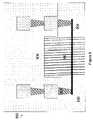
- FIG. 2shows the result of a process in accordance with the prior art.
- vias 202are patterned in the top of the cavity encapsulation layer 204 over the substrate 206 , either at the same time as the cavity encapsulation layer 204 is formed or with a separate release hole mask. After the release etch is performed, the vias 202 are then sealed by depositing a layer of the seal material on top of the cavity encapsulation layer 204 , thereby plugging the vias 202 .
- FIG. 3shows the result of a process in accordance with one embodiment of the present invention.
- the sacrificial materialis patterned in such a way as to leave release tabs 302 on the side of the cavity body which protrude from the cavity encapsulation layer 304 over the substrate 306 .
- lateral release channelsare created in select locations which are positioned underneath the cavity encapsulation layer 304 .
- the cavity encapsulation layer 304is deposited and then etched to remove undesired portions of the cavity encapsulation layer 304 and leave portions of the cavity encapsulation layer 304 that will enclose the cavity.
- the release channelsare exposed because they extend beyond the final structure of structure of the cavity encapsulation layer 304 .
- a release etchis then performed to remove the sacrificial layers.
- the channelsare then sealed by depositing a layer of seal material (as described in above) on the cavity encapsulation layer 304 , thereby plugging the channels.
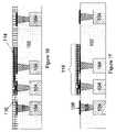
- FIG. 4Ashows top and cross-sectional views of the release tabs 402 in accordance with one embodiment of the present invention.
- the release tabs 402may be of a height equal to the height of both sacrificial layers and extend from the cavity 406 . As explained below however, thinner release channels can also be created.
- the release tabs 402extend beyond the sidewalls of the encapsulating layer 404 . In the embodiment shown in FIG. 4A , the release tabs 402 are substantially straight such that there is a direct line of sight path from the release tabs 402 to the cavity 406 .
- FIG. 4Bshows another release tab 412 configuration, where the channels 418 extending from the release tabs 412 to the cavity 416 are dog-legged or zig-zagged in shape.
- the release tabs 412extend from the sidewalls of the encapsulating layer 414 .
- This designwill impede the line-of-site of the release channel 418 , thereby helping to seal the cavity 416 without sealing material being deposited on the device contained therein.
- the dashed linethere is no line of sight path from the release tabs 412 to the cavity 416 .
- the molecules of the sealing layerduring deposition, may travel in a substantially linear path without scattering and thus deposit on the walls leading to the cavity 416 rather than within the cavity 416 itself.
- FIG. 4Cshows a single sided, multi tab 422 release channels 428 extending from the cavity 426 through the sidewalls of the encapsulating layer 424 in accordance with another embodiment of the present invention.
- FIG. 4Dshows a dual ended release tab 432 extending through the sidewalls of the encapsulating layer 434 to the cavity 436 in accordance with another embodiment of the present invention.
- FIGS. 5A and 5Bshow additional release channel configurations.
- the release channels 502 , 512 formed through the sidewalls of the encapsulating layers 506 , 516are blocked by deposited metal layers 504 , 514 , 518 .
- These metal layers 504 , 514 , 518effectively reduce the height of the release channels 502 , 512 .
- the metal layers 504 , 514 , 518reduce the opening of the release channels 502 , 512 and thus reduce the amount of sealing material that may deposit within the release channels 502 , 512 and cavity during the second encapsulating layer deposition.
- This configurationcan be achieved by having a single layer ( FIG. 5A ) or multiple layers ( FIG.
- the metal layers 504 , 514 , 518may be formed by blanket depositing a metal layer, depositing a photoresist layer thereon, exposing the photoresist, developing the photoresist, removing the developed (or undeveloped photoresist) to form a mask, and then exposing the metal layers 504 , 514 , 518 through the mask to an etchant to remove undesired portions of the metal layers 504 , 514 , 518 . Thereafter, the mask may be removed.
- the benefit of the metal layers 504 , 514 , 518is that after the sacrificial layers have been removed, the material used for the sealing layer may not enter into the cavity.
- the metal layers 504 , 514 , 518make the entrance into the cavity smaller and reduce the amount of material that may enter the cavity. If material enters into the cavity, it may adversely affect the performance of the device contained therein.
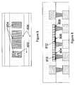
- FIG. 6shows another release channel configuration where the height of the release channel has been controlled by removal of material from the release channel itself.
- a guard ring trench 602is etched into the structure during the patterning of the interconnect via between the landing electrodes 604 and the cantilever in the lower sacrificial layer 606 .
- the trench 602is etched to remove the lower sacrificial layer in the region of the subsequent release channels underneath the cap metal.
- the second sacrificial layeris deposited in the trench 602 .
- the trench 602which will serve as the release channel, is as thick as the second sacrificial layer rather than both the first and second sacrificial layers. The smaller thickness decreases may reduce the amount of encapsulating material that enters into the cavity when the cavity is sealed.
- the sacrificial layermust be able to be selectively etched with respect to the embedded cantilever and encapsulation material.
- the cantilever, electrodes and encapsulation materialsare selected from the group of materials comprising Al, Cu, Ti, TiN, Ta, TaN, Ru, Pt, WN, WNC or any combination thereof.
- the potential sacrificial layers which can be usedare Si, SiN (using a Fluorine plasma based release etch), organic, polyimide, amorphous-Carbon (using a Hydrogen or Oxygen plasma based release etch) or SiO 2 (using a wet HF etch or vapor HF release etch).
- the encapsulation layercan be made from another material, for example, SiO 2 , in which case a SiO 2 sacrificial layer cannot be used.
- the release layermay be deposited in multiple steps to form a sacrificial layer at the bottom and top of the cantilever.
- the height of the release channelmay be determined by the total thickness of the sacrificial layers deposited (i.e., both top and bottom layers).
- the bottom sacrificial layercan be patterned to anchor or connect the cantilever to the underlying metal.
- small contact bumpsmay be formed by performing a multi-step deposition of the sacrificial layer with an intermediate patterning step between depositions.
- the sacrificial layer in the release channelcan also be patterned and etched without incurring any extra mask cost or complexity. This allows thinner release channels to be used. As will be appreciated, thinner release channels will help the sealing process.
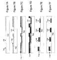
- FIGS. 7A-7Frepresent the formation of release channels in accordance with one embodiment of the present invention.
- a first sacrificial layer 704is deposited over a substrate 702 and then a via 706 is formed through the sacrificial layer 704 .
- the sacrificial layer 704may be deposited by a spin-on process.
- the via 706may be formed by conventional patterning and etching as described above.
- a second sacrificial layer 708may be deposited over the first sacrificial layer 704 .
- a via 710may be formed in the second sacrificial layer 708 .
- a third sacrificial layer 712may be deposited.
- a fourth sacrificial layer 714may also be deposited over the third sacrificial layer 712 .
- a via 716may be formed in the third sacrificial layer 712 prior to depositing the fourth sacrificial layer 714 .
- the sacrificial layers 704 , 708 , 712 , 714may then be patterned and an encapsulating layer 720 may be deposited thereon so that a plurality of release channels 718 A- 718 D are formed of varying height.
- the height of the release tabsmay be less than the height of the cavity.
- the release tabsmay be formed by N sacrificial layers extending out from the cavity where N is less than M.
- FIGS. 8-11show the results of a different aluminum BEOL cavities which can be implemented using the above discussed embodiments.
- the MEMS devices used in these examplesare all cantilever devices. As will be appreciated however, other MEMS/NEMS devices can be added and connected to surrounding interconnects, as required. Examples of other MEMS/NEMS devices include, but are not limited to, resonators, gyroscopes, accelerometers and pressure sensors.
- FIG. 8shows a cantilever 812 in contact with a first electrode 804 and movable between a position in contact with a second electrode 808 and a position away from the second electrode 808 .
- a third electrode 806is also present within the cavity 810 .
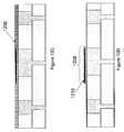
- FIG. 9shows a structure 900 having a cavity 902 that extends to a height greater than a single dielectric layer 906 .
- An element 904may connect vias 908 through the cavity 902 .
- the element 904may be a MEMS device.
- the cavity 902may have a height greater than a single dielectric layer 906 to permit bigger elements 904 to be within the cavity 902 .
- the cavity 902may span more than the height of a single dielectric layer 906 .
- the cavity 902may span a height of one or more dielectric layers 906 and thus, one or more interconnect layers.
- the device within the cavity 902may be positioned to be either horizontally placed or vertically placed. By horizontally placed, it is understood that the device will lie in a plane substantially parallel to the substrate upon which the device is formed. By vertically placed, it is understood that the device will lie in a plan substantially perpendicular to the substrate upon which the device is formed.
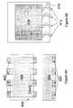
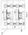
- FIG. 10shows a plurality of cavities 1002 within a structure 1000 having a plurality of metal interconnects 1004 , vias 1006 , and inter-metal dielectric layers 1008 .
- the cavities 1002may be encapsulated by a metal encapsulating layer 1010 .
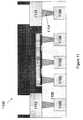
- FIG. 11shows a structure 1100 having a cavity 1102 formed above a plurality of vias 1104 , interconnects 1106 , and a dielectric layer 1108 .
- the cavity 1102may be encapsulated by a passivation layer 1110 such as silicon dioxide or silicon nitride.
- the passivation layer 1110may be adjacent to a plurality of bond pads 1112 .
- FIGS. 12A-12Ganother embodiment of the encapsulating method will now be described.
- the embodimentdescribes the fabrication of a micro-cavity in a 90 nm copper CMOS BEOL.
- this embodimentwill be described using the formation of a cantilever device as an example of a MEMS device which may be encapsulated.
- the embodiment described belowis suitable for the encapsulation of any Cu BEOL technology node.
- FIG. 12Adescribes the first step of the method. More specifically, the first step comprises using normal CMOS process steps to fabricate a wafer up to a predetermined level within a copper CMOS BEOL. The step further comprises depositing a first sacrificial layer 1202 . Similarly to the previous embodiment, the thickness of the sacrificial layer is chosen to permit correct operation of the enclosed MEMS device.
- a conductive layeris deposited over the lower sacrificial layer to form the cantilever 1204 of the cantilever device.
- the conductive layercomprises titanium nitride.
- the conductive layeris then patterned using conventional lithography and etch processes in order to form the desired cantilever 1204 .
- the third step in the methodis shown in FIG. 12C .
- a second sacrificial layer 1206is deposited on the wafer surface over the patterned cantilever 1204 .
- the coating of this second sacrificial layer 1206effectively seals the MEMS element prior to the fabrication of the micro-cavity 1208 .
- FIG. 12Dshows the result of the fourth step of the method.
- a via structure 1210is patterned in the upper sacrificial layer to form an interconnect from the underlying CMOS to the anchor point of the cantilever device.
- FIG. 12EThe result of the fifth step of the present invention is shown in FIG. 12E .
- This stepcomprises the formation of the anchor 1212 and electrode 1214 of the cantilever 1204 .
- a thick layer of metalis deposited and then patterned and etched to form the required electrode areas for the device.
- An additionally electrode 1216may also be present.
- FIG. 12Fshows the sixth step of the method in accordance with the present invention.
- a typical CMOS BEOL sequenceis continued.
- the deposited IMD layerseffectively seal the, as of yet, unreleased micro-cavity 1208 within the BEOL materials.
- Dual damascene interconnectionsare made to the electrodes patterned in the previous step in order to connect the device out to the underlying CMOS.
- Viasare then patterned and etched down to the buried micro-cavity sacrificial layer.
- the sacrificial layeris then removed by using a dry plasma etch to leave behind free standing MEMS element 1218 .
- the micro-cavityis effectively sealed with the deposition of the next interconnect IMD.
- FIGS. 13 and 14Other configurations for copper BEOL cavity implementations are shown in FIGS. 13 and 14 .
- the MEMS devices used in these examplesare all cantilever devices. As will be appreciated however, other MEMS/NEMS devices can be added and connected to surrounding interconnects, as required. Examples of other MEMS/NEMS devices include, but are not limited to, resonators, gyroscopes, accelerometers and pressure sensors.
- three electrodes 1302are present in the cavity 1306 .
- a plurality of vias 1304are present that connect the interconnects 1308 to the interconnects 1310 above the cavity 1306 .
- FIG. 14shows a plurality of cavities 1402 each with a cantilevers 1410 .
- An anchor 1404 and a plurality of electrodes 1408 , 1406may be present.
- multiple devicesmay be within a single cavity.
- the multiple devicesmay be capable of performing the same purpose or function that a single device may perform.
- the multiple devicesmay also be capable of performing different purposes or functions such that a plurality of devices within a same cavity.
- multiple devices placed within multiple cavitiesmay be present with each device capable of performing the same or different function.
- Each of the cavities discussed hereinmay fit within the interlayer dielectric layer.
- release tabsBy patterning the sacrificial layers to form release tabs that extend beyond the sidewall of the encapsulating layer, additional masking steps to pattern and etch release holes through the top of the encapsulating layer are not necessary.
- the release tabscan be formed during the initial patterning of the sacrificial layers and encapsulating layer. Thus, a cavity may be formed in a more efficient manner according to the embodiments described herein.
Landscapes
- Engineering & Computer Science (AREA)
- Microelectronics & Electronic Packaging (AREA)
- Manufacturing & Machinery (AREA)
- Micromachines (AREA)
Abstract
Description
Claims (18)
Priority Applications (3)
| Application Number | Priority Date | Filing Date | Title |
|---|---|---|---|
| US12/266,457US7993950B2 (en) | 2008-04-30 | 2008-11-06 | System and method of encapsulation |
| PCT/US2009/042028WO2009134838A2 (en) | 2008-04-30 | 2009-04-29 | System and method of encapsulation |
| TW098114440ATWI353339B (en) | 2008-04-30 | 2009-04-30 | System and method of encapsulation |
Applications Claiming Priority (2)
| Application Number | Priority Date | Filing Date | Title |
|---|---|---|---|
| US12607208P | 2008-04-30 | 2008-04-30 | |
| US12/266,457US7993950B2 (en) | 2008-04-30 | 2008-11-06 | System and method of encapsulation |
Publications (2)
| Publication Number | Publication Date |
|---|---|
| US20090275163A1 US20090275163A1 (en) | 2009-11-05 |
| US7993950B2true US7993950B2 (en) | 2011-08-09 |
Family
ID=41255745
Family Applications (1)
| Application Number | Title | Priority Date | Filing Date |
|---|---|---|---|
| US12/266,457Active2029-06-25US7993950B2 (en) | 2008-04-30 | 2008-11-06 | System and method of encapsulation |
Country Status (3)
| Country | Link |
|---|---|
| US (1) | US7993950B2 (en) |
| TW (1) | TWI353339B (en) |
| WO (1) | WO2009134838A2 (en) |
Cited By (3)
| Publication number | Priority date | Publication date | Assignee | Title |
|---|---|---|---|---|
| US20100127340A1 (en)* | 2008-11-21 | 2010-05-27 | Kabushiki Kaisha Toshiba | Mems package and method of manufacturing the mems package |
| US9209778B2 (en) | 2013-03-15 | 2015-12-08 | Infineon Technologies Dresden Gmbh | Microelectromechanical resonators |
| US9511560B2 (en) | 2012-04-13 | 2016-12-06 | Infineon Technologies Ag | Processing a sacrificial material during manufacture of a microfabricated product |
Families Citing this family (42)
| Publication number | Priority date | Publication date | Assignee | Title |
|---|---|---|---|---|
| US7943410B2 (en)* | 2008-12-10 | 2011-05-17 | Stmicroelectronics, Inc. | Embedded microelectromechanical systems (MEMS) semiconductor substrate and related method of forming |
| WO2010111601A2 (en)* | 2009-03-26 | 2010-09-30 | Semprius, Inc. | Methods of forming printable integrated circuit devices and devices formed thereby |
| TWI559388B (en)* | 2010-03-01 | 2016-11-21 | 煙草動力學股份有限公司 | Cmp process flow for mems |
| KR20130100232A (en)* | 2010-04-09 | 2013-09-10 | 퀄컴 엠이엠에스 테크놀로지스, 인크. | Mechanical layer of an electromechanical device and methods of forming the same |
| US8956903B2 (en) | 2010-06-25 | 2015-02-17 | International Business Machines Corporation | Planar cavity MEMS and related structures, methods of manufacture and design structures |
| US8535966B2 (en)* | 2010-07-27 | 2013-09-17 | International Business Machines Corporation | Horizontal coplanar switches and methods of manufacture |
| US8906750B2 (en) | 2011-01-04 | 2014-12-09 | Commissariat A L'energie Atomique Et Aux Energies Alternatives | Method of encapsulation of a microcomponent |
| FR2970116B1 (en)* | 2011-01-04 | 2013-08-16 | Commissariat Energie Atomique | METHOD FOR ENCAPSULATING A MICROCOMPONENT |
| US8963159B2 (en) | 2011-04-04 | 2015-02-24 | Qualcomm Mems Technologies, Inc. | Pixel via and methods of forming the same |
| US9134527B2 (en) | 2011-04-04 | 2015-09-15 | Qualcomm Mems Technologies, Inc. | Pixel via and methods of forming the same |
| US9112003B2 (en) | 2011-12-09 | 2015-08-18 | Asm International N.V. | Selective formation of metallic films on metallic surfaces |
| TWI661072B (en) | 2014-02-04 | 2019-06-01 | 荷蘭商Asm Ip控股公司 | Selective deposition of metals, metal oxides, and dielectrics |
| US10047435B2 (en) | 2014-04-16 | 2018-08-14 | Asm Ip Holding B.V. | Dual selective deposition |
| US9637371B2 (en)* | 2014-07-25 | 2017-05-02 | Semiconductor Manufacturing International (Shanghai) Corporation | Membrane transducer structures and methods of manufacturing same using thin-film encapsulation |
| US9490145B2 (en) | 2015-02-23 | 2016-11-08 | Asm Ip Holding B.V. | Removal of surface passivation |
| US10428421B2 (en) | 2015-08-03 | 2019-10-01 | Asm Ip Holding B.V. | Selective deposition on metal or metallic surfaces relative to dielectric surfaces |
| US10121699B2 (en) | 2015-08-05 | 2018-11-06 | Asm Ip Holding B.V. | Selective deposition of aluminum and nitrogen containing material |
| US10343186B2 (en) | 2015-10-09 | 2019-07-09 | Asm Ip Holding B.V. | Vapor phase deposition of organic films |
| US10695794B2 (en) | 2015-10-09 | 2020-06-30 | Asm Ip Holding B.V. | Vapor phase deposition of organic films |
| US10814349B2 (en) | 2015-10-09 | 2020-10-27 | Asm Ip Holding B.V. | Vapor phase deposition of organic films |
| US10461047B2 (en)* | 2015-10-29 | 2019-10-29 | Intel Corporation | Metal-free frame design for silicon bridges for semiconductor packages |
| KR102182550B1 (en) | 2016-04-18 | 2020-11-25 | 에이에스엠 아이피 홀딩 비.브이. | Method of forming induced self-assembly layer on a substrate |
| US10204782B2 (en) | 2016-04-18 | 2019-02-12 | Imec Vzw | Combined anneal and selective deposition process |
| US11081342B2 (en) | 2016-05-05 | 2021-08-03 | Asm Ip Holding B.V. | Selective deposition using hydrophobic precursors |
| US10453701B2 (en) | 2016-06-01 | 2019-10-22 | Asm Ip Holding B.V. | Deposition of organic films |
| US10373820B2 (en) | 2016-06-01 | 2019-08-06 | Asm Ip Holding B.V. | Deposition of organic films |
| US11430656B2 (en) | 2016-11-29 | 2022-08-30 | Asm Ip Holding B.V. | Deposition of oxide thin films |
| JP7169072B2 (en) | 2017-02-14 | 2022-11-10 | エーエスエム アイピー ホールディング ビー.ブイ. | Selective passivation and selective deposition |
| US11501965B2 (en) | 2017-05-05 | 2022-11-15 | Asm Ip Holding B.V. | Plasma enhanced deposition processes for controlled formation of metal oxide thin films |
| KR102684628B1 (en) | 2017-05-16 | 2024-07-15 | 에이에스엠 아이피 홀딩 비.브이. | Selective PEALD of oxides on dielectrics |
| US10900120B2 (en) | 2017-07-14 | 2021-01-26 | Asm Ip Holding B.V. | Passivation against vapor deposition |
| JP7146690B2 (en) | 2018-05-02 | 2022-10-04 | エーエスエム アイピー ホールディング ビー.ブイ. | Selective layer formation using deposition and removal |
| JP2020056104A (en) | 2018-10-02 | 2020-04-09 | エーエスエム アイピー ホールディング ビー.ブイ. | Selective passivation and selective deposition |
| US11965238B2 (en) | 2019-04-12 | 2024-04-23 | Asm Ip Holding B.V. | Selective deposition of metal oxides on metal surfaces |
| US11139163B2 (en) | 2019-10-31 | 2021-10-05 | Asm Ip Holding B.V. | Selective deposition of SiOC thin films |
| CN113086937B (en)* | 2019-12-23 | 2024-03-19 | 财团法人工业技术研究院 | MEMS device and method for manufacturing the same |
| US11939212B2 (en) | 2019-12-23 | 2024-03-26 | Industrial Technology Research Institute | MEMS device, manufacturing method of the same, and integrated MEMS module using the same |
| TWI865747B (en) | 2020-03-30 | 2024-12-11 | 荷蘭商Asm Ip私人控股有限公司 | Simultaneous selective deposition of two different materials on two different surfaces |
| TW202140832A (en) | 2020-03-30 | 2021-11-01 | 荷蘭商Asm Ip私人控股有限公司 | Selective deposition of silicon oxide on metal surfaces |
| TWI862807B (en) | 2020-03-30 | 2024-11-21 | 荷蘭商Asm Ip私人控股有限公司 | Selective deposition of silicon oxide on dielectric surfaces relative to metal surfaces |
| JP7519248B2 (en)* | 2020-09-18 | 2024-07-19 | 新光電気工業株式会社 | Wiring board and manufacturing method thereof |
| DE102023207522B3 (en) | 2023-08-04 | 2024-10-31 | Fraunhofer-Gesellschaft zur Förderung der angewandten Forschung eingetragener Verein | Method for producing an electrically conductive channel structure in a substrate |
Citations (79)
| Publication number | Priority date | Publication date | Assignee | Title |
|---|---|---|---|---|
| US4761219A (en) | 1987-01-23 | 1988-08-02 | Anelva Corporation | Magnetron sputtering etching apparatus |
| JPS63198378A (en) | 1987-02-13 | 1988-08-17 | Nissan Motor Co Ltd | Vibration sensor manufacturing method |
| JPS63307758A (en) | 1987-06-09 | 1988-12-15 | Nec Corp | Integrated circuit device |
| JPH05297413A (en) | 1991-12-19 | 1993-11-12 | Sony Corp | Liquid crystal display device |
| US5270264A (en) | 1991-12-20 | 1993-12-14 | Intel Corporation | Process for filling submicron spaces with dielectric |
| US5279669A (en) | 1991-12-13 | 1994-01-18 | International Business Machines Corporation | Plasma reactor for processing substrates comprising means for inducing electron cyclotron resonance (ECR) and ion cyclotron resonance (ICR) conditions |
| US5292370A (en) | 1992-08-14 | 1994-03-08 | Martin Marietta Energy Systems, Inc. | Coupled microwave ECR and radio-frequency plasma source for plasma processing |
| US5346578A (en) | 1992-11-04 | 1994-09-13 | Novellus Systems, Inc. | Induction plasma source |
| US5504026A (en) | 1995-04-14 | 1996-04-02 | Analog Devices, Inc. | Methods for planarization and encapsulation of micromechanical devices in semiconductor processes |
| US5589082A (en)* | 1992-12-11 | 1996-12-31 | The Regents Of The University Of California | Microelectromechanical signal processor fabrication |
| EP0751546A2 (en) | 1995-06-22 | 1997-01-02 | Rockwell International Corporation | Micro electromechanical RF switch |
| WO1997007517A2 (en) | 1995-08-21 | 1997-02-27 | Honeywell, Inc. | Electrostatically operated, micromechanical capacitor |
| US5614055A (en) | 1993-08-27 | 1997-03-25 | Applied Materials, Inc. | High density plasma CVD and etching reactor |
| EP0783182A2 (en) | 1996-01-08 | 1997-07-09 | Siemens Aktiengesellschaft | Fuse in a semiconductor integrated circuit |
| JPH09257618A (en) | 1996-03-26 | 1997-10-03 | Toyota Central Res & Dev Lab Inc | Capacitive pressure sensor and manufacturing method thereof |
| US5872058A (en) | 1997-06-17 | 1999-02-16 | Novellus Systems, Inc. | High aspect ratio gapfill process by using HDP |
| JPH11177067A (en) | 1997-12-09 | 1999-07-02 | Sony Corp | Memory element and memory array |
| US5919548A (en) | 1996-10-11 | 1999-07-06 | Sandia Corporation | Chemical-mechanical polishing of recessed microelectromechanical devices |
| US6012336A (en) | 1995-09-06 | 2000-01-11 | Sandia Corporation | Capacitance pressure sensor |
| US6051121A (en) | 1996-01-22 | 2000-04-18 | Micron Technology Inc | Deposition chamber with a biased substrate configuration |
| WO2000024021A1 (en) | 1998-10-22 | 2000-04-27 | Northeastern University | Micromechanical switching devices |
| WO2000033089A2 (en) | 1998-12-02 | 2000-06-08 | Formfactor, Inc. | Lithographic contact elements |
| JP2000186931A (en) | 1998-12-21 | 2000-07-04 | Murata Mfg Co Ltd | Small-sized electronic component and its manufacture, and via hole forming method for the small-sized electronic component |
| EP1041629A1 (en) | 1999-03-31 | 2000-10-04 | International Business Machines Corporation | Manufacturing of cavity fuses on gate conductor level |
| US6174820B1 (en) | 1999-02-16 | 2001-01-16 | Sandia Corporation | Use of silicon oxynitride as a sacrificial material for microelectromechanical devices |
| US6174850B1 (en) | 1998-07-24 | 2001-01-16 | Atofina | Cleaning or drying compositions based on 1,1,1,2,3,4,4,5,5,5-decafluoropentane |
| WO2001031664A1 (en) | 1999-10-28 | 2001-05-03 | Hrl Laboratories, Llc. | Optically controlled mem switches |
| JP2001133703A (en) | 1999-11-04 | 2001-05-18 | Seiko Epson Corp | Method and apparatus for manufacturing device having structure on semiconductor substrate |
| WO2001056066A1 (en) | 2000-01-28 | 2001-08-02 | Reflectivity, Inc. | A method for forming a micromechanical device |
| US20010023991A1 (en) | 1997-02-27 | 2001-09-27 | Yumi Kakuhara | Semiconductor device and method of its fabrication |
| WO2001083363A1 (en) | 2000-05-04 | 2001-11-08 | Silverbrook Research Pty Ltd | Improved thermal bend actuator |
| WO2001092842A2 (en) | 2000-05-30 | 2001-12-06 | Ic Mechanics, Inc. | Manufacture of mems structures in sealed cavity using dry-release mems device encapsulation |
| US20020011645A1 (en) | 1999-04-30 | 2002-01-31 | Claude L. Bertin | Electronic fuse structure and method of manufacturing |
| WO2002016150A1 (en) | 2000-08-23 | 2002-02-28 | Reflectivity, Inc. | Transition metal dielectric alloy materials for mems |
| US6391150B1 (en) | 1997-09-26 | 2002-05-21 | Sca Hygiene Products Gmbh | Process for treating waste paper to form a spore-free base tissue |
| DE10056716A1 (en) | 2000-11-15 | 2002-05-23 | Bosch Gmbh Robert | Microstructured component used as a micromechanical sensor element comprises a microstructure with a layer system consisting of a hermetically sealed layer and a polymer layer |
| US6395150B1 (en) | 1998-04-01 | 2002-05-28 | Novellus Systems, Inc. | Very high aspect ratio gapfill using HDP |
| US20020064906A1 (en) | 2000-03-22 | 2002-05-30 | Ziptronix | Three dimensional device integration method and integrated device |
| WO2002063657A2 (en) | 2000-11-07 | 2002-08-15 | Sarnoff Corporation | Microelectronic mechanical system (mems) switch and method of fabrication |
| JP2002280470A (en) | 2001-03-22 | 2002-09-27 | Aisin Seiki Co Ltd | Semiconductor device and manufacturing method thereof |
| US20020193037A1 (en) | 1997-05-14 | 2002-12-19 | Hofmann James J. | Anodically bonded elements for flat-panel display |
| US20030001221A1 (en) | 2001-02-03 | 2003-01-02 | Frank Fischer | Micromechanical component as well as a method for producing a micromechanical component |
| JP2003035874A (en) | 2001-07-23 | 2003-02-07 | Nikon Corp | Thin film slide connection mechanism, method of manufacturing the same, mirror device and optical switch using the same |
| JP2003506871A (en) | 1999-08-02 | 2003-02-18 | ハネウエル・インコーポレーテッド | Dual wafer attachment method |
| WO2003028059A1 (en) | 2001-09-21 | 2003-04-03 | Hrl Laboratories, Llc | Mems switches and methods of making same |
| US20030138986A1 (en) | 2001-09-13 | 2003-07-24 | Mike Bruner | Microelectronic mechanical system and methods |
| US20030148550A1 (en) | 2001-11-07 | 2003-08-07 | International Business Machines Corporation | Method of fabricating micro-electromechanical switches on cmos compatible substrates |
| US20030153116A1 (en)* | 2000-05-30 | 2003-08-14 | Carley L. Richard | Encapsulation of MEMS devices using pillar-supported caps |
| WO2003069645A1 (en) | 2002-02-11 | 2003-08-21 | Memscap | Method for the production of a microswitch-type micro component |
| WO2003085719A2 (en) | 2002-04-02 | 2003-10-16 | Dow Global Technologies Inc. | Process for making air gap containing semiconducting devices and resulting semiconducting device |
| US6635509B1 (en) | 2002-04-12 | 2003-10-21 | Dalsa Semiconductor Inc. | Wafer-level MEMS packaging |
| US20040157426A1 (en) | 2003-02-07 | 2004-08-12 | Luc Ouellet | Fabrication of advanced silicon-based MEMS devices |
| US20040159532A1 (en) | 2002-07-18 | 2004-08-19 | Svetlana Tatic-Lucic | Recessed electrode for electrostatically actuated structures |
| EP1450406A1 (en) | 2003-02-19 | 2004-08-25 | Cavendish Kinetics Limited | Micro fuse |
| US20040166603A1 (en)* | 2003-02-25 | 2004-08-26 | Carley L. Richard | Micromachined assembly with a multi-layer cap defining a cavity |
| US20040188785A1 (en) | 2001-11-09 | 2004-09-30 | Cunningham Shawn Jay | Trilayered beam MEMS device and related methods |
| WO2004096696A1 (en) | 2003-04-25 | 2004-11-11 | Cavendish Kinetics Ltd | Method of manufacturing a micro-mechanical element |
| US20040245588A1 (en) | 2003-06-03 | 2004-12-09 | Nikkel Eric L. | MEMS device and method of forming MEMS device |
| US20050017313A1 (en) | 2002-08-07 | 2005-01-27 | Chang-Feng Wan | System and method of fabricating micro cavities |
| US20050037608A1 (en) | 2003-08-13 | 2005-02-17 | Ibm | Deep filled vias |
| US6861277B1 (en) | 2003-10-02 | 2005-03-01 | Hewlett-Packard Development Company, L.P. | Method of forming MEMS device |
| WO2005060002A1 (en) | 2003-12-18 | 2005-06-30 | Canon Kabushiki Kaisha | Semiconductor integrated circuit, operating method thereof, and ic card including the circuit |
| WO2005061376A1 (en) | 2003-12-24 | 2005-07-07 | Cavendish Kinetics Limited | Method for containing a device and a corresponding device |
| US20050164127A1 (en) | 2001-06-15 | 2005-07-28 | Reid Jason S. | Method for removing a sacrificial material with a compressed fluid |
| US6936494B2 (en) | 2002-10-23 | 2005-08-30 | Rutgers, The State University Of New Jersey | Processes for hermetically packaging wafer level microscopic structures |
| FR2874213A1 (en) | 2004-08-13 | 2006-02-17 | Commissariat Energie Atomique | Fabrication of a device incorporating an encapsulated micro-system for microelectromechanical systems such as radiofrequency devices, comprises providing micro-system, sacrificial material, depositing and flattening encapsulation layer |
| US20060108675A1 (en) | 2004-11-19 | 2006-05-25 | International Business Machines Incorporated | Apparatus and methods for encapsulating microelectromechanical (MEM) devices on a wafer scale |
| US20060134825A1 (en) | 2004-12-20 | 2006-06-22 | Dcamp Jon B | Injection-molded package for MEMS inertial sensor |
| WO2006077565A1 (en) | 2005-01-24 | 2006-07-27 | University College Cork - National University Of Ireland, Cork; | Packaging of micro devices |
| US20060220173A1 (en) | 2005-04-01 | 2006-10-05 | Skyworks Solutions, Inc. | Wafer level package including a device wafer integrated with a passive component |
| US7163896B1 (en) | 2003-12-10 | 2007-01-16 | Novellus Systems, Inc. | Biased H2 etch process in deposition-etch-deposition gap fill |
| WO2007015097A1 (en) | 2005-08-03 | 2007-02-08 | Cavendish Kinetics Ltd | Memory bitcell and method of using the same |
| WO2007017672A1 (en) | 2005-08-05 | 2007-02-15 | Cavendish Kinetics Ltd | Method of integrating an element |
| US7211525B1 (en) | 2005-03-16 | 2007-05-01 | Novellus Systems, Inc. | Hydrogen treatment enhanced gap fill |
| WO2007060416A1 (en) | 2005-11-22 | 2007-05-31 | Cavendish Kinetics Limited | A micro-electromechanical device and method of making the same |
| WO2007060414A1 (en) | 2005-11-22 | 2007-05-31 | Cavendish Kinetics Limited | Method of enclosing a micro-electromechanical element |
| US7235281B2 (en) | 2002-12-24 | 2007-06-26 | Interuniversitair Microelektronica Centrum (Imec) | Method for the closure of openings in a film |
| US7329586B2 (en) | 2005-06-24 | 2008-02-12 | Applied Materials, Inc. | Gapfill using deposition-etch sequence |
| US7344996B1 (en) | 2005-06-22 | 2008-03-18 | Novellus Systems, Inc. | Helium-based etch process in deposition-etch-deposition gap fill |
- 2008
- 2008-11-06USUS12/266,457patent/US7993950B2/enactiveActive
- 2009
- 2009-04-29WOPCT/US2009/042028patent/WO2009134838A2/enactiveApplication Filing
- 2009-04-30TWTW098114440Apatent/TWI353339B/enactive
Patent Citations (82)
| Publication number | Priority date | Publication date | Assignee | Title |
|---|---|---|---|---|
| US4761219A (en) | 1987-01-23 | 1988-08-02 | Anelva Corporation | Magnetron sputtering etching apparatus |
| JPS63198378A (en) | 1987-02-13 | 1988-08-17 | Nissan Motor Co Ltd | Vibration sensor manufacturing method |
| JPS63307758A (en) | 1987-06-09 | 1988-12-15 | Nec Corp | Integrated circuit device |
| US5279669A (en) | 1991-12-13 | 1994-01-18 | International Business Machines Corporation | Plasma reactor for processing substrates comprising means for inducing electron cyclotron resonance (ECR) and ion cyclotron resonance (ICR) conditions |
| JPH05297413A (en) | 1991-12-19 | 1993-11-12 | Sony Corp | Liquid crystal display device |
| US5270264A (en) | 1991-12-20 | 1993-12-14 | Intel Corporation | Process for filling submicron spaces with dielectric |
| US5292370A (en) | 1992-08-14 | 1994-03-08 | Martin Marietta Energy Systems, Inc. | Coupled microwave ECR and radio-frequency plasma source for plasma processing |
| US5346578A (en) | 1992-11-04 | 1994-09-13 | Novellus Systems, Inc. | Induction plasma source |
| US5589082A (en)* | 1992-12-11 | 1996-12-31 | The Regents Of The University Of California | Microelectromechanical signal processor fabrication |
| US5614055A (en) | 1993-08-27 | 1997-03-25 | Applied Materials, Inc. | High density plasma CVD and etching reactor |
| US5504026A (en) | 1995-04-14 | 1996-04-02 | Analog Devices, Inc. | Methods for planarization and encapsulation of micromechanical devices in semiconductor processes |
| EP0751546A2 (en) | 1995-06-22 | 1997-01-02 | Rockwell International Corporation | Micro electromechanical RF switch |
| WO1997007517A2 (en) | 1995-08-21 | 1997-02-27 | Honeywell, Inc. | Electrostatically operated, micromechanical capacitor |
| US6012336A (en) | 1995-09-06 | 2000-01-11 | Sandia Corporation | Capacitance pressure sensor |
| EP0783182A2 (en) | 1996-01-08 | 1997-07-09 | Siemens Aktiengesellschaft | Fuse in a semiconductor integrated circuit |
| US6051121A (en) | 1996-01-22 | 2000-04-18 | Micron Technology Inc | Deposition chamber with a biased substrate configuration |
| JPH09257618A (en) | 1996-03-26 | 1997-10-03 | Toyota Central Res & Dev Lab Inc | Capacitive pressure sensor and manufacturing method thereof |
| US5919548A (en) | 1996-10-11 | 1999-07-06 | Sandia Corporation | Chemical-mechanical polishing of recessed microelectromechanical devices |
| US20010023991A1 (en) | 1997-02-27 | 2001-09-27 | Yumi Kakuhara | Semiconductor device and method of its fabrication |
| US20020193037A1 (en) | 1997-05-14 | 2002-12-19 | Hofmann James J. | Anodically bonded elements for flat-panel display |
| US5872058A (en) | 1997-06-17 | 1999-02-16 | Novellus Systems, Inc. | High aspect ratio gapfill process by using HDP |
| US6391150B1 (en) | 1997-09-26 | 2002-05-21 | Sca Hygiene Products Gmbh | Process for treating waste paper to form a spore-free base tissue |
| JPH11177067A (en) | 1997-12-09 | 1999-07-02 | Sony Corp | Memory element and memory array |
| US6395150B1 (en) | 1998-04-01 | 2002-05-28 | Novellus Systems, Inc. | Very high aspect ratio gapfill using HDP |
| US6174850B1 (en) | 1998-07-24 | 2001-01-16 | Atofina | Cleaning or drying compositions based on 1,1,1,2,3,4,4,5,5,5-decafluoropentane |
| WO2000024021A1 (en) | 1998-10-22 | 2000-04-27 | Northeastern University | Micromechanical switching devices |
| WO2000033089A2 (en) | 1998-12-02 | 2000-06-08 | Formfactor, Inc. | Lithographic contact elements |
| JP2000186931A (en) | 1998-12-21 | 2000-07-04 | Murata Mfg Co Ltd | Small-sized electronic component and its manufacture, and via hole forming method for the small-sized electronic component |
| US6174820B1 (en) | 1999-02-16 | 2001-01-16 | Sandia Corporation | Use of silicon oxynitride as a sacrificial material for microelectromechanical devices |
| EP1041629A1 (en) | 1999-03-31 | 2000-10-04 | International Business Machines Corporation | Manufacturing of cavity fuses on gate conductor level |
| US20020011645A1 (en) | 1999-04-30 | 2002-01-31 | Claude L. Bertin | Electronic fuse structure and method of manufacturing |
| JP2003506871A (en) | 1999-08-02 | 2003-02-18 | ハネウエル・インコーポレーテッド | Dual wafer attachment method |
| WO2001031664A1 (en) | 1999-10-28 | 2001-05-03 | Hrl Laboratories, Llc. | Optically controlled mem switches |
| JP2001133703A (en) | 1999-11-04 | 2001-05-18 | Seiko Epson Corp | Method and apparatus for manufacturing device having structure on semiconductor substrate |
| WO2001056066A1 (en) | 2000-01-28 | 2001-08-02 | Reflectivity, Inc. | A method for forming a micromechanical device |
| US20020064906A1 (en) | 2000-03-22 | 2002-05-30 | Ziptronix | Three dimensional device integration method and integrated device |
| WO2001083363A1 (en) | 2000-05-04 | 2001-11-08 | Silverbrook Research Pty Ltd | Improved thermal bend actuator |
| US7008812B1 (en)* | 2000-05-30 | 2006-03-07 | Ic Mechanics, Inc. | Manufacture of MEMS structures in sealed cavity using dry-release MEMS device encapsulation |
| WO2001092842A2 (en) | 2000-05-30 | 2001-12-06 | Ic Mechanics, Inc. | Manufacture of mems structures in sealed cavity using dry-release mems device encapsulation |
| US20030153116A1 (en)* | 2000-05-30 | 2003-08-14 | Carley L. Richard | Encapsulation of MEMS devices using pillar-supported caps |
| WO2002016150A1 (en) | 2000-08-23 | 2002-02-28 | Reflectivity, Inc. | Transition metal dielectric alloy materials for mems |
| WO2002063657A2 (en) | 2000-11-07 | 2002-08-15 | Sarnoff Corporation | Microelectronic mechanical system (mems) switch and method of fabrication |
| DE10056716A1 (en) | 2000-11-15 | 2002-05-23 | Bosch Gmbh Robert | Microstructured component used as a micromechanical sensor element comprises a microstructure with a layer system consisting of a hermetically sealed layer and a polymer layer |
| US20030001221A1 (en) | 2001-02-03 | 2003-01-02 | Frank Fischer | Micromechanical component as well as a method for producing a micromechanical component |
| JP2002280470A (en) | 2001-03-22 | 2002-09-27 | Aisin Seiki Co Ltd | Semiconductor device and manufacturing method thereof |
| US20050164127A1 (en) | 2001-06-15 | 2005-07-28 | Reid Jason S. | Method for removing a sacrificial material with a compressed fluid |
| JP2003035874A (en) | 2001-07-23 | 2003-02-07 | Nikon Corp | Thin film slide connection mechanism, method of manufacturing the same, mirror device and optical switch using the same |
| US20030138986A1 (en) | 2001-09-13 | 2003-07-24 | Mike Bruner | Microelectronic mechanical system and methods |
| WO2003028059A1 (en) | 2001-09-21 | 2003-04-03 | Hrl Laboratories, Llc | Mems switches and methods of making same |
| US20030148550A1 (en) | 2001-11-07 | 2003-08-07 | International Business Machines Corporation | Method of fabricating micro-electromechanical switches on cmos compatible substrates |
| US20040188785A1 (en) | 2001-11-09 | 2004-09-30 | Cunningham Shawn Jay | Trilayered beam MEMS device and related methods |
| WO2003069645A1 (en) | 2002-02-11 | 2003-08-21 | Memscap | Method for the production of a microswitch-type micro component |
| WO2003085719A2 (en) | 2002-04-02 | 2003-10-16 | Dow Global Technologies Inc. | Process for making air gap containing semiconducting devices and resulting semiconducting device |
| US6635509B1 (en) | 2002-04-12 | 2003-10-21 | Dalsa Semiconductor Inc. | Wafer-level MEMS packaging |
| US20040159532A1 (en) | 2002-07-18 | 2004-08-19 | Svetlana Tatic-Lucic | Recessed electrode for electrostatically actuated structures |
| US20050017313A1 (en) | 2002-08-07 | 2005-01-27 | Chang-Feng Wan | System and method of fabricating micro cavities |
| US20080308920A1 (en)* | 2002-08-07 | 2008-12-18 | Chang-Feng Wan | System and method of fabricating micro cavities |
| US6936494B2 (en) | 2002-10-23 | 2005-08-30 | Rutgers, The State University Of New Jersey | Processes for hermetically packaging wafer level microscopic structures |
| US7235281B2 (en) | 2002-12-24 | 2007-06-26 | Interuniversitair Microelektronica Centrum (Imec) | Method for the closure of openings in a film |
| US20040157426A1 (en) | 2003-02-07 | 2004-08-12 | Luc Ouellet | Fabrication of advanced silicon-based MEMS devices |
| EP1450406A1 (en) | 2003-02-19 | 2004-08-25 | Cavendish Kinetics Limited | Micro fuse |
| US20040166603A1 (en)* | 2003-02-25 | 2004-08-26 | Carley L. Richard | Micromachined assembly with a multi-layer cap defining a cavity |
| WO2004096696A1 (en) | 2003-04-25 | 2004-11-11 | Cavendish Kinetics Ltd | Method of manufacturing a micro-mechanical element |
| US20040245588A1 (en) | 2003-06-03 | 2004-12-09 | Nikkel Eric L. | MEMS device and method of forming MEMS device |
| US20050037608A1 (en) | 2003-08-13 | 2005-02-17 | Ibm | Deep filled vias |
| US6861277B1 (en) | 2003-10-02 | 2005-03-01 | Hewlett-Packard Development Company, L.P. | Method of forming MEMS device |
| US7163896B1 (en) | 2003-12-10 | 2007-01-16 | Novellus Systems, Inc. | Biased H2 etch process in deposition-etch-deposition gap fill |
| WO2005060002A1 (en) | 2003-12-18 | 2005-06-30 | Canon Kabushiki Kaisha | Semiconductor integrated circuit, operating method thereof, and ic card including the circuit |
| WO2005061376A1 (en) | 2003-12-24 | 2005-07-07 | Cavendish Kinetics Limited | Method for containing a device and a corresponding device |
| US20070004096A1 (en)* | 2003-12-24 | 2007-01-04 | Heuvelman Willem M | Method for containing a device and a corresponding device |
| FR2874213A1 (en) | 2004-08-13 | 2006-02-17 | Commissariat Energie Atomique | Fabrication of a device incorporating an encapsulated micro-system for microelectromechanical systems such as radiofrequency devices, comprises providing micro-system, sacrificial material, depositing and flattening encapsulation layer |
| US20060108675A1 (en) | 2004-11-19 | 2006-05-25 | International Business Machines Incorporated | Apparatus and methods for encapsulating microelectromechanical (MEM) devices on a wafer scale |
| US20060134825A1 (en) | 2004-12-20 | 2006-06-22 | Dcamp Jon B | Injection-molded package for MEMS inertial sensor |
| WO2006077565A1 (en) | 2005-01-24 | 2006-07-27 | University College Cork - National University Of Ireland, Cork; | Packaging of micro devices |
| US7211525B1 (en) | 2005-03-16 | 2007-05-01 | Novellus Systems, Inc. | Hydrogen treatment enhanced gap fill |
| US20060220173A1 (en) | 2005-04-01 | 2006-10-05 | Skyworks Solutions, Inc. | Wafer level package including a device wafer integrated with a passive component |
| US7344996B1 (en) | 2005-06-22 | 2008-03-18 | Novellus Systems, Inc. | Helium-based etch process in deposition-etch-deposition gap fill |
| US7329586B2 (en) | 2005-06-24 | 2008-02-12 | Applied Materials, Inc. | Gapfill using deposition-etch sequence |
| WO2007015097A1 (en) | 2005-08-03 | 2007-02-08 | Cavendish Kinetics Ltd | Memory bitcell and method of using the same |
| WO2007017672A1 (en) | 2005-08-05 | 2007-02-15 | Cavendish Kinetics Ltd | Method of integrating an element |
| WO2007060416A1 (en) | 2005-11-22 | 2007-05-31 | Cavendish Kinetics Limited | A micro-electromechanical device and method of making the same |
| WO2007060414A1 (en) | 2005-11-22 | 2007-05-31 | Cavendish Kinetics Limited | Method of enclosing a micro-electromechanical element |
Non-Patent Citations (23)
| Title |
|---|
| Chan, et al., "Comprehensive Static Characterization of Vertical Electrostatically Actuated Polysilicon Beams", vol. 16, No. 4, Oct. 1999, pp. 58-65. |
| International Preliminary Report and Written Opinion for International Application No. PCT/GB2006/004350 dated May 27, 2008. |
| International Preliminary Report and Written Opinion for International Application No. PCT/GB2006/004354 dated May 27, 2008. |
| International Preliminary Report and Written Opinion for International Application No. PCT/GB2006/2959 dated Feb. 5, 2008. |
| International Preliminary Report on Patentability for International Application No. PCT/GB2004/001773 dated Jun. 22, 2008. |
| International Preliminary Report on Patentability for International Application No. PCT/GB2004/005122 dated Nov. 16, 2005. |
| International search report and written opinion for PCT/US2009/042028 (CK056PCT) dated May 4, 2010. |
| International Search Report for International Application No. PCT/GB2004/001773 dated Sep. 6, 2004. |
| International Search Report for International Application No. PCT/GB2004/005122 dated Mar. 2, 2005. |
| International Search Report for International Application No. PCT/GB2006/002959 dated Oct. 25, 2006. |
| International Search Report for International Application No. PCT/GB2006/004350 dated Mar. 12, 2007. |
| International Search Report for International Application No. PCT/GB2006/004354 dated Mar. 12, 2007. |
| Liu et al., "Sealing of micro machined cavities using chemical vapour deposition methods: characterisation and optimisation", J. MEMS, 8, pp. 135-145, 1999. |
| Logan, "RF Diode Sputter Etching and Deposition," Handbook of Plasma Processing Technology, pp. 140-159. |
| Mercado et al., "A mechanical approach to overcome RF MEMS switch stiction problem", vol. conf. 53, dated May 27, 2003, pp. 377-384. |
| Notification of Reasons for Rejection dated Feb. 17, 2009 for Japanese Patent Application No. 2006-546296 (CK004JP) and English translation thereof. |
| Notification of the First Office Action for Chinese Patent Application No. 200480039028.0 (CK004-China) dated Feb. 27, 2009. |
| Office Action for European Patent Application No. 04805944.8 dated Jun. 22, 2009 (CK004EP). |
| Park et al., "Wafer-scale film encapsulation of micromachined accelerometers", The 12th Int. Conf. on Solid State Sensors, Actuators and Microsystems, Boston, Jun. 8-12, 2003, pp. 1903-1906. |
| Stahl et al., "Thin film encapsulation of acceleration sensors using polysilicon sacrificial layers", The 12th int. Conf. on Solid State Sensors, Actuators and Microsystems, Boston, Jun. 8-12, 2003, pp. 1899-1902. |
| Written Opinion for International Application No. PCT/GB2004/001773 dated Sep. 6, 2004. |
| Written Opinion for International Application No. PCT/GB2004/005122 dated Feb. 28, 2005. |
| Zavracky et al., "Micromechanical Switches Fabricated Using Nickel Surface Micromachining", Journal of Microelectromechanical Systems, IEEE Service Center, Piscataway, NJ, US, vol. 6, No. 1, dated Mar. 1997. |
Cited By (5)
| Publication number | Priority date | Publication date | Assignee | Title |
|---|---|---|---|---|
| US20100127340A1 (en)* | 2008-11-21 | 2010-05-27 | Kabushiki Kaisha Toshiba | Mems package and method of manufacturing the mems package |
| US8283737B2 (en)* | 2008-11-21 | 2012-10-09 | Kabushiki Kaisha Toshiba | MEMS package and method of manufacturing the MEMS package |
| US9511560B2 (en) | 2012-04-13 | 2016-12-06 | Infineon Technologies Ag | Processing a sacrificial material during manufacture of a microfabricated product |
| US9209778B2 (en) | 2013-03-15 | 2015-12-08 | Infineon Technologies Dresden Gmbh | Microelectromechanical resonators |
| US9641153B2 (en) | 2013-03-15 | 2017-05-02 | Infineon Technologies Dresden Gmbh | Method of forming a resonator |
Also Published As
| Publication number | Publication date |
|---|---|
| WO2009134838A2 (en) | 2009-11-05 |
| TW200951062A (en) | 2009-12-16 |
| US20090275163A1 (en) | 2009-11-05 |
| TWI353339B (en) | 2011-12-01 |
| WO2009134838A3 (en) | 2010-06-17 |
Similar Documents
| Publication | Publication Date | Title |
|---|---|---|
| US7993950B2 (en) | System and method of encapsulation | |
| JP4658966B2 (en) | Method for housing micromechanical element and method for forming micromechanical element | |
| US9988264B2 (en) | Method of fabricating integrated structure for MEMS device and semiconductor device | |
| US9859818B2 (en) | Micro-device with a cavity | |
| KR100367137B1 (en) | Integrated circuits with borderless vias | |
| US9472504B2 (en) | Semiconductor having a high aspect ratio via | |
| EP1734001B1 (en) | Method of packaging MEMS at wafer level | |
| US9708177B2 (en) | MEMS device anchoring | |
| EP2542499B1 (en) | Cmp process flow for mems | |
| JP2011049303A (en) | Electric component and method of manufacturing the same | |
| US20250074766A1 (en) | Method and system for fabricating a mems device | |
| EP2584598B1 (en) | Method of producing a semiconductor device comprising a through-substrate via and a capping layer and corresponding semiconductor device | |
| KR101366554B1 (en) | A semiconductor device and a method of manufacturing the same | |
| JP2007311797A (en) | Semiconductor device including sealed nanotube structure and method for manufacturing the same | |
| JPH104092A (en) | Method of fabricating semiconductor device | |
| KR101391290B1 (en) | A semiconductor device and a method of manufacturing the same | |
| US9156681B2 (en) | Semiconductor device and method for manufacturing the same | |
| KR101366553B1 (en) | A semiconductor device and a method of manufacturing the same | |
| KR100607815B1 (en) | Method for Forming Metal Line of Semiconductor Device | |
| KR20070069883A (en) | Semiconductor device and manufacturing method |
Legal Events
| Date | Code | Title | Description |
|---|---|---|---|
| AS | Assignment | Owner name:CAVENDISH KINETICS, LTD., UNITED KINGDOM Free format text:ASSIGNMENT OF ASSIGNORS INTEREST;ASSIGNORS:LACEY, JOSEPH DAMIAN GORDON, MR.;RENAULT, MICKAEL, MR.;JOSHI, VIKRAM, MR.;AND OTHERS;REEL/FRAME:021799/0916;SIGNING DATES FROM 20081028 TO 20081029 Owner name:CAVENDISH KINETICS, LTD., UNITED KINGDOM Free format text:ASSIGNMENT OF ASSIGNORS INTEREST;ASSIGNORS:LACEY, JOSEPH DAMIAN GORDON, MR.;RENAULT, MICKAEL, MR.;JOSHI, VIKRAM, MR.;AND OTHERS;SIGNING DATES FROM 20081028 TO 20081029;REEL/FRAME:021799/0916 | |
| STCF | Information on status: patent grant | Free format text:PATENTED CASE | |
| FEPP | Fee payment procedure | Free format text:PAT HOLDER CLAIMS SMALL ENTITY STATUS, ENTITY STATUS SET TO SMALL (ORIGINAL EVENT CODE: LTOS); ENTITY STATUS OF PATENT OWNER: SMALL ENTITY | |
| FPAY | Fee payment | Year of fee payment:4 | |
| MAFP | Maintenance fee payment | Free format text:PAYMENT OF MAINTENANCE FEE, 8TH YR, SMALL ENTITY (ORIGINAL EVENT CODE: M2552); ENTITY STATUS OF PATENT OWNER: SMALL ENTITY Year of fee payment:8 | |
| AS | Assignment | Owner name:QORVO US, INC., NORTH CAROLINA Free format text:INTANGIBLE PROPERTY PURCHASE AGREEMENT;ASSIGNOR:CAVENDISH KINETICS LIMITED;REEL/FRAME:058983/0599 Effective date:20200622 | |
| FEPP | Fee payment procedure | Free format text:ENTITY STATUS SET TO UNDISCOUNTED (ORIGINAL EVENT CODE: BIG.); ENTITY STATUS OF PATENT OWNER: LARGE ENTITY | |
| MAFP | Maintenance fee payment | Free format text:PAYMENT OF MAINTENANCE FEE, 12TH YEAR, LARGE ENTITY (ORIGINAL EVENT CODE: M1553); ENTITY STATUS OF PATENT OWNER: LARGE ENTITY Year of fee payment:12 |