US7990025B1 - Silicon package with embedded oscillator - Google Patents
Silicon package with embedded oscillatorDownload PDFInfo
- Publication number
- US7990025B1 US7990025B1US11/698,480US69848007AUS7990025B1US 7990025 B1US7990025 B1US 7990025B1US 69848007 AUS69848007 AUS 69848007AUS 7990025 B1US7990025 B1US 7990025B1
- Authority
- US
- United States
- Prior art keywords
- enclosure
- cover
- silicon
- elements
- base member
- Prior art date
- Legal status (The legal status is an assumption and is not a legal conclusion. Google has not performed a legal analysis and makes no representation as to the accuracy of the status listed.)
- Expired - Fee Related, expires
Links
- 239000010703siliconSubstances0.000titleclaimsabstractdescription34
- 229910052710siliconInorganic materials0.000titleclaimsabstractdescription34
- XUIMIQQOPSSXEZ-UHFFFAOYSA-NSiliconChemical compound[Si]XUIMIQQOPSSXEZ-UHFFFAOYSA-N0.000titleclaimsabstractdescription29
- BASFCYQUMIYNBI-UHFFFAOYSA-NplatinumChemical compound[Pt]BASFCYQUMIYNBI-UHFFFAOYSA-N0.000claimsdescription22
- 239000013078crystalSubstances0.000claimsdescription14
- 238000010438heat treatmentMethods0.000claimsdescription14
- 239000000463materialSubstances0.000claimsdescription14
- 229910052697platinumInorganic materials0.000claimsdescription11
- MCMNRKCIXSYSNV-UHFFFAOYSA-NZirconium dioxideChemical compoundO=[Zr]=OMCMNRKCIXSYSNV-UHFFFAOYSA-N0.000claimsdescription8
- IJGRMHOSHXDMSA-UHFFFAOYSA-NAtomic nitrogenChemical compoundN#NIJGRMHOSHXDMSA-UHFFFAOYSA-N0.000claimsdescription6
- 238000007906compressionMethods0.000claimsdescription5
- PCHJSUWPFVWCPO-UHFFFAOYSA-NgoldChemical compound[Au]PCHJSUWPFVWCPO-UHFFFAOYSA-N0.000claimsdescription5
- 229910052737goldInorganic materials0.000claimsdescription5
- 239000010931goldSubstances0.000claimsdescription5
- RTAQQCXQSZGOHL-UHFFFAOYSA-NTitaniumChemical compound[Ti]RTAQQCXQSZGOHL-UHFFFAOYSA-N0.000claimsdescription4
- 229910052594sapphireInorganic materials0.000claimsdescription4
- 239000010980sapphireSubstances0.000claimsdescription4
- HBMJWWWQQXIZIP-UHFFFAOYSA-Nsilicon carbideChemical compound[Si+]#[C-]HBMJWWWQQXIZIP-UHFFFAOYSA-N0.000claimsdescription4
- 229910010271silicon carbideInorganic materials0.000claimsdescription4
- 229910052715tantalumInorganic materials0.000claimsdescription4
- GUVRBAGPIYLISA-UHFFFAOYSA-Ntantalum atomChemical compound[Ta]GUVRBAGPIYLISA-UHFFFAOYSA-N0.000claimsdescription4
- 229910052719titaniumInorganic materials0.000claimsdescription4
- 239000010936titaniumSubstances0.000claimsdescription4
- 239000007789gasSubstances0.000claimsdescription3
- 239000001307heliumSubstances0.000claimsdescription3
- 229910052734heliumInorganic materials0.000claimsdescription3
- SWQJXJOGLNCZEY-UHFFFAOYSA-Nhelium atomChemical compound[He]SWQJXJOGLNCZEY-UHFFFAOYSA-N0.000claimsdescription3
- 239000001257hydrogenSubstances0.000claimsdescription3
- 229910052739hydrogenInorganic materials0.000claimsdescription3
- 125000004435hydrogen atomChemical class[H]*0.000claimsdescription3
- 239000011261inert gasSubstances0.000claimsdescription3
- 229910052757nitrogenInorganic materials0.000claimsdescription3
- 238000013022ventingMethods0.000claimsdescription2
- NJPPVKZQTLUDBO-UHFFFAOYSA-NnovaluronChemical compoundC1=C(Cl)C(OC(F)(F)C(OC(F)(F)F)F)=CC=C1NC(=O)NC(=O)C1=C(F)C=CC=C1FNJPPVKZQTLUDBO-UHFFFAOYSA-N0.000abstract1
- 238000000034methodMethods0.000description9
- 239000010453quartzSubstances0.000description6
- VYPSYNLAJGMNEJ-UHFFFAOYSA-Nsilicon dioxideInorganic materialsO=[Si]=OVYPSYNLAJGMNEJ-UHFFFAOYSA-N0.000description6
- 239000011521glassSubstances0.000description4
- 230000008901benefitEffects0.000description3
- 230000015556catabolic processEffects0.000description3
- 239000000356contaminantSubstances0.000description3
- 238000006731degradation reactionMethods0.000description3
- 230000006866deteriorationEffects0.000description3
- 238000007373indentationMethods0.000description3
- 238000004519manufacturing processMethods0.000description3
- RYGMFSIKBFXOCR-UHFFFAOYSA-NCopperChemical compound[Cu]RYGMFSIKBFXOCR-UHFFFAOYSA-N0.000description2
- 230000015572biosynthetic processEffects0.000description2
- 238000005219brazingMethods0.000description2
- 229910052802copperInorganic materials0.000description2
- 239000010949copperSubstances0.000description2
- 239000006023eutectic alloySubstances0.000description2
- GPYPVKIFOKLUGD-UHFFFAOYSA-Ngold indiumChemical compound[In].[Au]GPYPVKIFOKLUGD-UHFFFAOYSA-N0.000description2
- 229910052751metalInorganic materials0.000description2
- 239000002184metalSubstances0.000description2
- 238000012986modificationMethods0.000description2
- 230000004048modificationEffects0.000description2
- 238000003466weldingMethods0.000description2
- 241000321453Paranthias colonusSpecies0.000description1
- 230000009286beneficial effectEffects0.000description1
- 238000011109contaminationMethods0.000description1
- 230000001627detrimental effectEffects0.000description1
- 239000003344environmental pollutantSubstances0.000description1
- 229910000154gallium phosphateInorganic materials0.000description1
- 230000006698inductionEffects0.000description1
- GQYHUHYESMUTHG-UHFFFAOYSA-Nlithium niobateChemical compound[Li+].[O-][Nb](=O)=OGQYHUHYESMUTHG-UHFFFAOYSA-N0.000description1
- 150000002739metalsChemical class0.000description1
- 229910021421monocrystalline siliconInorganic materials0.000description1
- 231100000719pollutantToxicity0.000description1
- 150000003376siliconChemical class0.000description1
- 239000007787solidSubstances0.000description1
- 238000010897surface acoustic wave methodMethods0.000description1
Images


Classifications
- H—ELECTRICITY
- H03—ELECTRONIC CIRCUITRY
- H03H—IMPEDANCE NETWORKS, e.g. RESONANT CIRCUITS; RESONATORS
- H03H9/00—Networks comprising electromechanical or electro-acoustic elements; Electromechanical resonators
- H03H9/02—Details
- H03H9/05—Holders or supports
- H03H9/10—Mounting in enclosures
- H03H9/1007—Mounting in enclosures for bulk acoustic wave [BAW] devices
- H03H9/1014—Mounting in enclosures for bulk acoustic wave [BAW] devices the enclosure being defined by a frame built on a substrate and a cap, the frame having no mechanical contact with the BAW device
- H—ELECTRICITY
- H01—ELECTRIC ELEMENTS
- H01L—SEMICONDUCTOR DEVICES NOT COVERED BY CLASS H10
- H01L23/00—Details of semiconductor or other solid state devices
- H01L23/02—Containers; Seals
- H01L23/04—Containers; Seals characterised by the shape of the container or parts, e.g. caps, walls
- H—ELECTRICITY
- H03—ELECTRONIC CIRCUITRY
- H03H—IMPEDANCE NETWORKS, e.g. RESONANT CIRCUITS; RESONATORS
- H03H9/00—Networks comprising electromechanical or electro-acoustic elements; Electromechanical resonators
- H03H9/02—Details
- H03H9/05—Holders or supports
- H03H9/0504—Holders or supports for bulk acoustic wave devices
- H03H9/0514—Holders or supports for bulk acoustic wave devices consisting of mounting pads or bumps
- H—ELECTRICITY
- H03—ELECTRONIC CIRCUITRY
- H03H—IMPEDANCE NETWORKS, e.g. RESONANT CIRCUITS; RESONATORS
- H03H9/00—Networks comprising electromechanical or electro-acoustic elements; Electromechanical resonators
- H03H9/02—Details
- H03H9/05—Holders or supports
- H03H9/0538—Constructional combinations of supports or holders with electromechanical or other electronic elements
- H03H9/0547—Constructional combinations of supports or holders with electromechanical or other electronic elements consisting of a vertical arrangement
- H03H9/0552—Constructional combinations of supports or holders with electromechanical or other electronic elements consisting of a vertical arrangement the device and the other elements being mounted on opposite sides of a common substrate
- H—ELECTRICITY
- H01—ELECTRIC ELEMENTS
- H01L—SEMICONDUCTOR DEVICES NOT COVERED BY CLASS H10
- H01L2924/00—Indexing scheme for arrangements or methods for connecting or disconnecting semiconductor or solid-state bodies as covered by H01L24/00
- H01L2924/0001—Technical content checked by a classifier
- H01L2924/0002—Not covered by any one of groups H01L24/00, H01L24/00 and H01L2224/00
Definitions
- the present inventionis directed to the field of electronic devices, such as piezoelectric devices.
- piezoelectric deviceincludes resonators, filters and surface acoustic wave devices. More particularly, the present invention is directed to a hermetic silicon package for such devices and a method of making a surface mountable electronic component utilizing such a package.
- piezoelectric devicessuch as quartz resonators, packaged in a glass housing, for use in aerospace applications.
- the glass bubblecan be replaced by a copper housing.
- copper packagesare subject to collapse as the metal reaches a softening point and the internal vacuum may draw contaminants into the cavity. This permits the piezoelectric device housed therein to be subject to whatever contaminants may be contained in the ambient environment, leading to degradation of its properties.
- the proposed deviceinvolves silicon-quartz-silicon bonding, a difficult proposition at best, given the dissimilarity of the materials, made all the more risky by doubling the extent of circumferential area subject to failure by doubling the number of bonds needed. For many applications, this bond failure may not significantly impact the performance of the housed components but, as has been noted, in the demanding environment of aerospace, even the slightest degradation must be resisted as intolerable.
- a hermetically packaged electronic devicecomprising a) an enclosure made of a plurality of elements each made of a material selected from a group consisting of silicon, titanium, zirconia, silicon carbide, sapphire, and tantalum, including a base element and a cover element, the cover element having contoured edges; b) means bonding the plurality of elements together; c) an Application Specific Integrated Circuit (ASIC) oscillator embedded in the enclosure; d) a piezoelectric device secured within the enclosure; e) a metallic layer bonded to an upper surface of the lower element, the contoured edges of the cover element exposing end portions of the metallic layer to permit easy connection to electronic circuitry outside the enclosure.
- the materialis silicon.
- the vacated enclosuremay be filled with a gas selected from a group consisting of hydrogen, nitrogen, helium, and other inert gases.
- the plurality of elements forming the enclosureis secured together by thermo-compression bonding means performed at high temperature.
- the base member and the coverprovide means of electrical contact to the piezoelectric device obviating need for leads and wires within and protruding through a wall portion of the package.
- the coveris contoured to leave portions of the heating element exposed so that electrical connection can be made thereto.
- the base member and the coverare each comprised of single metallic silicon crystals.
- the heating elementcomprises a non-venting, electrically conductive element bonded to an upper surface of the base member which is preferably secured to the base member by the same bonding means used to secure the plurality of enclosure elements together.
- the heating elementis made from a material selected from the group consisting of platinum and gold, most preferably platinum so that the same element may also function as a temperature sensing means.
- the thermo-compression bonding meansis performed in a temperature range of between 300° C. and 800° C.
- FIG. 1Ais top view of a first embodiment of the silicon package of the present invention with the cover removed;
- FIG. 1Bis a cross-sectional view of the first embodiment as seen along line 1 B- 1 B in FIG. 1A ;
- FIG. 1Cis a cross-sectional view of the first embodiment as seen along line 1 C- 1 C in FIG. 1A ;
- FIG. 2Ais a top view of the cover of the first embodiment of the silicon package
- FIG. 2Bis a side view of the cover of the first embodiment of the silicon package
- FIG. 3Ais a top view of a second embodiment of the silicon package of the present invention with the cover removed;
- FIG. 3Bis a cross-sectional side view of the base member of the second embodiment as seen along line 3 B- 3 B of FIG. 3A ;
- FIG. 3Cis a cross-sectional side view of the base member of the second embodiment as seen along line 3 C- 3 C of FIG. 3A ;
- FIG. 4Ais a top view of a second embodiment of the cover of the present invention.
- FIG. 4Bis a side view of the cover for the second embodiment
- FIG. 5Ais a cross-sectional bottom view taken along line 5 - 5 in FIG. 5B ;
- FIG. 5Bis a cross-sectional side view of the cover depicted in FIG. 5A ;
- FIG. 6is schematic depiction of a layout for forming a plurality of covers of a third embodiment.
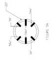
- FIG. 1BA first embodiment of a first embodiment of the silicon package incorporating an embedded Application Specific Integrated Circuit (ASIC) oscillator of the present invention is depicted in FIG. 1B generally at 20 .
- Silicon package 20includes a base member 22 manufactured from a single crystal of metallic silicon.
- the term “metallic silicon”means having zero valence.
- the cover 32is manufactured from a single crystal of metallic silicon. Cover 32 has a hollowed out region 34 to receive the piezoelectric device, in this case a quartz crystal resonator 40 .
- base member 22has a pair of electrodes 28 , 28 A which may be gold ribbon, first electrode 28 providing electrical connection to embedded ASIC oscillator circuit 25 and second electrode 28 A providing electrical connection to thermal control circuit 26 .
- electrodes 28 , 28 Amay be platinum.
- a third circuit 29 A, 29 Bprovide electric feed through for resonator 40 which sits atop and is bonded to circuit elements 29 A, 29 B.
- the term “embedded”indicates that ASIC oscillator circuit 25 is actually etched in the silicon of base member 22 and is not a separate chip which must be bonded to the base member 22 .
- cover 32is contoured with three sets of indentations 36 A, 36 B, and 36 C being formed on each lateral edge 35 , 37 , respectively.
- These sets of indentations 36 A, 36 B, and 36 Coverlie and, therefore, expose the end portions of electrodes 28 A, 28 B, 29 A, and 29 B to enable connection to the electrical power source external to the hermetically sealed cavity after the vacuum has been formed in a manner consistent with that described below.
- An array 60 of covers 32are depicted in FIG. 6 .
- a similar array (not shown) of base members 22is configured with electrodes 28 A, 28 B, 29 A, and 29 B in place.
- Quartz crystal resonator 40is attached to base member 22 by any of a variety of known high temperature methods performed in a temperature range from 300° C. and 800° C., a brazing technique using a gold indium eutectic alloy performed at a temperature of 495° C. being preferred.
- each cover 32 in array 60is attached to each base member 22 within a vacuum chamber capable of pulling a vacuum in the range of between 1 ⁇ 10 ⁇ 6 and 1 ⁇ 10 ⁇ 10 torr to remove all potential pollutants from the cavity created by the hollowed out portion 34 as well as from the elements mounted therein. It will be understood that should a technological advance be made in the area of vacuum equipment where a vacuum of 1 ⁇ 10 ⁇ 11 torr or less would be possible, such a vacuum would also not depart from the scope of this invention.
- FIGS. 3A-3CA second embodiment of the surface mountable electronic component including a hermetic package is shown in FIGS. 3A-3C generally at 20 ′.
- the base member 22 ′has a hollowed out region 24 ′.
- the hollowed out regionis provided with shoulders 21 ′ which can support the resonator 40 ′ above and in non-contacting relationship to the ASIC oscillator circuit 25 ′ and the thermal control circuit 26 ′.
- the p-doping processrenders the silicon non-conductive.
- the ends of the electronic circuits 28 ′A, 28 ′B, 29 ′A and 29 ′Bextend up on the rim 23 ′ of the hollowed out region 24 ′.
- the cover 32 ′which is, in this case, flat, is contoured defining indentations 36 ′A, 36 ′B, 36 ′C overlie and expose the ends of electronic circuits 28 ′A, 28 ′B, 29 ′A and 29 ′B to enable attachment to the electronic power source external to the hermetically sealed container 20 ′ after its formation.
- first and second embodimentshave been described as having base members and covers made of single crystal silicon brazed using gold indium eutectic alloy, it is contemplated that other materials could be used.
- siliconis the preferred material, other materials including titanium, zirconia, silicon carbide, sapphire, and tantalum could be used.
- the brazing technique set forth hereinis preferred method of affixing the two halves of the package together as well as fixing the electronic component in place, it is contemplated other bonding techniques including laser welding, E-beam welding, anodic bonding, and induction heating could be used.
- the preferred electronic componentis an ultra-stable oscillator in the form of a quartz crystal
- other electronic componentsincluding a gallium orthophosphate crystal and a lithium niobate crystal, could be utilized in this hermetic package.
- FIGS. 5A and 5BA third embodiment is shown in FIGS. 5A and 5B generally at 20 ′′.
- three single crystal metallic silicon elements 22 ′′, 32 ′′ and 52 ′′are bonded together using the techniques described with respect to the first and second embodiments.
- a metallic layer 50 ′′is bonded to the lower surface 33 ′′ of cover 32 ′′ within the hermetically sealed chamber 55 ′′.
- Material for metallic layer 50 ′′will be selected from a group consisting of gold and platinum. Both of these metals are suitable for use as heaters for chamber 55 ′′ by running a large current there through.
- An added benefit of a platinum metallic layer 50 ′′is that platinum can double as a thermal sensor within chamber 55 ′′by subjecting it to a lower amperage current.
- Cradle 52 ′′provides space for mounting oscillator 59 ′′ and electrical controls external to the hermetic chamber 55 ′′.
- the electronic component or device 57 ′′may be a piezoelectric component such as a quartz crystal or may take another form.
- oscillator 59 ′′ and associated electrical control elementsare mounted external to the hermetically sealed chamber 55 ′′ and electrical contacts 56 ′′ extend through element 52 ′′ to make connection with silicon element 32 ′′.
- Ribbons 58 ′′are wrapped around to the upper surface of cover 32 ′′ ( FIG. 5 a ) with ribbons 58 a ′′ providing electrical connection for heating/sensing element 50 ′′, ribbons 58 b ′′ providing electrical connection for electrical device 57 ′′ and the remaining ribbons 58 ′′ provided for another component which may be mounted within chamber 55 ′′.
- chamber 55 ′′it may be beneficial to fill chamber 55 ′′ with helium, hydrogen, nitrogen or an inert gas.
- the presence of the gascan facilitate the heating of the elements within the chamber to a uniform temperature.
Landscapes
- Physics & Mathematics (AREA)
- Acoustics & Sound (AREA)
- Condensed Matter Physics & Semiconductors (AREA)
- General Physics & Mathematics (AREA)
- Engineering & Computer Science (AREA)
- Computer Hardware Design (AREA)
- Microelectronics & Electronic Packaging (AREA)
- Power Engineering (AREA)
- Piezo-Electric Or Mechanical Vibrators, Or Delay Or Filter Circuits (AREA)
Abstract
Description
Claims (20)
Priority Applications (1)
| Application Number | Priority Date | Filing Date | Title |
|---|---|---|---|
| US11/698,480US7990025B1 (en) | 2004-09-01 | 2007-01-25 | Silicon package with embedded oscillator |
Applications Claiming Priority (3)
| Application Number | Priority Date | Filing Date | Title |
|---|---|---|---|
| US10/931,663US7061086B2 (en) | 2004-09-01 | 2004-09-01 | Silicon package for piezoelectric device |
| US11/156,353US7196405B1 (en) | 2004-09-01 | 2005-06-17 | Silicon package with integral heater |
| US11/698,480US7990025B1 (en) | 2004-09-01 | 2007-01-25 | Silicon package with embedded oscillator |
Related Parent Applications (1)
| Application Number | Title | Priority Date | Filing Date |
|---|---|---|---|
| US11/156,353Continuation-In-PartUS7196405B1 (en) | 2004-09-01 | 2005-06-17 | Silicon package with integral heater |
Publications (1)
| Publication Number | Publication Date |
|---|---|
| US7990025B1true US7990025B1 (en) | 2011-08-02 |
Family
ID=44314358
Family Applications (1)
| Application Number | Title | Priority Date | Filing Date |
|---|---|---|---|
| US11/698,480Expired - Fee RelatedUS7990025B1 (en) | 2004-09-01 | 2007-01-25 | Silicon package with embedded oscillator |
Country Status (1)
| Country | Link |
|---|---|
| US (1) | US7990025B1 (en) |
Cited By (4)
| Publication number | Priority date | Publication date | Assignee | Title |
|---|---|---|---|---|
| JP2013146003A (en)* | 2012-01-16 | 2013-07-25 | Seiko Epson Corp | Vibration device and electronic apparatus |
| US8610336B1 (en)* | 2011-09-30 | 2013-12-17 | Integrated Device Technology Inc | Microelectromechanical resonators having resistive heating elements therein configured to provide frequency tuning through convective heating of resonator bodies |
| US20170016859A1 (en)* | 2014-02-26 | 2017-01-19 | Aixtron Se | Device and method for determining the concentration of a vapor by means of an oscillating body sensor |
| US20220116018A1 (en)* | 2020-10-08 | 2022-04-14 | Samsung Electro-Mechanics Co., Ltd. | Bulk-acoustic wave filter device |
Citations (10)
| Publication number | Priority date | Publication date | Assignee | Title |
|---|---|---|---|---|
| US3969640A (en)* | 1972-03-22 | 1976-07-13 | Statek Corporation | Microresonator packaging and tuning |
| US5198716A (en)* | 1991-12-09 | 1993-03-30 | The United States Of America As Represented By The United States Department Of Energy | Micro-machined resonator |
| US5548178A (en)* | 1992-07-08 | 1996-08-20 | Matsushita Electric Industrial Co., Ltd. | Piezoelectric vibrator and manufacturing method thereof |
| US5919383A (en)* | 1996-12-06 | 1999-07-06 | Corning Incorporated | Package for a temperature-sensitive optical component with inner and outer containers and resistive element therein |
| US6060692A (en)* | 1998-09-02 | 2000-05-09 | Cts Corporation | Low power compact heater for piezoelectric device |
| US6507097B1 (en)* | 2001-11-29 | 2003-01-14 | Clarisay, Inc. | Hermetic package for pyroelectric-sensitive electronic device and method of manufacturing the same |
| US20040017004A1 (en)* | 2001-08-17 | 2004-01-29 | Takao Kasai | Electronic device and production method therefor |
| US6806557B2 (en)* | 2002-09-30 | 2004-10-19 | Motorola, Inc. | Hermetically sealed microdevices having a single crystalline silicon getter for maintaining vacuum |
| US20040217673A1 (en)* | 2003-03-20 | 2004-11-04 | Seiko Epson Corporation | Piezoelectric resonator |
| US20050056917A1 (en)* | 2003-09-15 | 2005-03-17 | Kwon Jong Oh | Wafer level package type FBAR device and manufacturing method thereof |
- 2007
- 2007-01-25USUS11/698,480patent/US7990025B1/ennot_activeExpired - Fee Related
Patent Citations (10)
| Publication number | Priority date | Publication date | Assignee | Title |
|---|---|---|---|---|
| US3969640A (en)* | 1972-03-22 | 1976-07-13 | Statek Corporation | Microresonator packaging and tuning |
| US5198716A (en)* | 1991-12-09 | 1993-03-30 | The United States Of America As Represented By The United States Department Of Energy | Micro-machined resonator |
| US5548178A (en)* | 1992-07-08 | 1996-08-20 | Matsushita Electric Industrial Co., Ltd. | Piezoelectric vibrator and manufacturing method thereof |
| US5919383A (en)* | 1996-12-06 | 1999-07-06 | Corning Incorporated | Package for a temperature-sensitive optical component with inner and outer containers and resistive element therein |
| US6060692A (en)* | 1998-09-02 | 2000-05-09 | Cts Corporation | Low power compact heater for piezoelectric device |
| US20040017004A1 (en)* | 2001-08-17 | 2004-01-29 | Takao Kasai | Electronic device and production method therefor |
| US6507097B1 (en)* | 2001-11-29 | 2003-01-14 | Clarisay, Inc. | Hermetic package for pyroelectric-sensitive electronic device and method of manufacturing the same |
| US6806557B2 (en)* | 2002-09-30 | 2004-10-19 | Motorola, Inc. | Hermetically sealed microdevices having a single crystalline silicon getter for maintaining vacuum |
| US20040217673A1 (en)* | 2003-03-20 | 2004-11-04 | Seiko Epson Corporation | Piezoelectric resonator |
| US20050056917A1 (en)* | 2003-09-15 | 2005-03-17 | Kwon Jong Oh | Wafer level package type FBAR device and manufacturing method thereof |
Non-Patent Citations (1)
| Title |
|---|
| Richard C. Jaeger, Introduction to Microelectronic Fabrication, 2002, Prentice Hall, Second Edition, pp. 1 and 2.* |
Cited By (6)
| Publication number | Priority date | Publication date | Assignee | Title |
|---|---|---|---|---|
| US8610336B1 (en)* | 2011-09-30 | 2013-12-17 | Integrated Device Technology Inc | Microelectromechanical resonators having resistive heating elements therein configured to provide frequency tuning through convective heating of resonator bodies |
| JP2013146003A (en)* | 2012-01-16 | 2013-07-25 | Seiko Epson Corp | Vibration device and electronic apparatus |
| US20170016859A1 (en)* | 2014-02-26 | 2017-01-19 | Aixtron Se | Device and method for determining the concentration of a vapor by means of an oscillating body sensor |
| US10267768B2 (en)* | 2014-02-26 | 2019-04-23 | Aixtron Se | Device and method for determining the concentration of a vapor by means of an oscillating body sensor |
| TWI658269B (en)* | 2014-02-26 | 2019-05-01 | Aixtron Se | Device and method for measuring steam concentration or partial pressure |
| US20220116018A1 (en)* | 2020-10-08 | 2022-04-14 | Samsung Electro-Mechanics Co., Ltd. | Bulk-acoustic wave filter device |
Similar Documents
| Publication | Publication Date | Title |
|---|---|---|
| US6700313B2 (en) | Piezoelectric resonator and assembly comprising the same enclosed in a case | |
| JP6247006B2 (en) | Electronic device, oscillator, and method of manufacturing electronic device | |
| US6606772B1 (en) | Method for manufacturing piezoelectric oscillator | |
| US20110241492A1 (en) | Quartz Crystal Device Using At-Cut Quartz Substrate and Manufacturing the Same | |
| JP2009165006A (en) | Piezoelectric vibrating piece, piezoelectric device, and tuning fork type piezoelectric vibrator frequency adjusting method | |
| JP2006279872A (en) | Piezoelectric vibrator, manufacturing method thereof, and manufacturing method of piezoelectric oscillator using the piezoelectric vibrator | |
| US7196405B1 (en) | Silicon package with integral heater | |
| US7990025B1 (en) | Silicon package with embedded oscillator | |
| JP2011218462A (en) | Mems device | |
| JP2007274610A (en) | Quartz crystal unit and crystal unit package | |
| WO2003044857A1 (en) | Package for electronic component, and piezoelectric vibrating device using the package for electronic component | |
| CN101552243B (en) | Crystal unit | |
| JP4545004B2 (en) | Piezoelectric oscillator | |
| JP5807755B2 (en) | Piezoelectric device | |
| JP2004214799A (en) | Piezoelectric oscillator and method of measuring piezoelectric oscillator | |
| JP2008131197A (en) | Piezoelectric vibrator and method for manufacturing the piezoelectric vibrator | |
| JP5123139B2 (en) | Piezoelectric device | |
| JP2005051513A (en) | Crystal oscillator | |
| JP4578231B2 (en) | Piezoelectric oscillator and manufacturing method thereof | |
| JP2009100213A (en) | Method of manufacturing piezoelectric vibrating apparatus | |
| JP4585908B2 (en) | Method for manufacturing piezoelectric device | |
| JP2007180885A (en) | Piezoelectric device | |
| US20250070748A1 (en) | Piezoelectric device | |
| JP2003133886A (en) | Crystal oscillator | |
| TWI449331B (en) | Crystal Oscillator |
Legal Events
| Date | Code | Title | Description |
|---|---|---|---|
| AS | Assignment | Owner name:BLILEY TECHNOLOGIES, INC., PENNSYLVANIA Free format text:ASSIGNMENT OF ASSIGNORS INTEREST;ASSIGNORS:FERREIRO, PABLO;MARTIN, KENNETH;CLINE, JOHN;REEL/FRAME:018848/0512 Effective date:20070125 | |
| AS | Assignment | Owner name:FIRST NATIONAL BANK OF PENNSYLVANIA, PENNSYLVANIA Free format text:SECURITY AGREEMENT;ASSIGNOR:BLILEY TECHNOLOGIES INCORPORATED;REEL/FRAME:023832/0662 Effective date:20100108 | |
| STCF | Information on status: patent grant | Free format text:PATENTED CASE | |
| FPAY | Fee payment | Year of fee payment:4 | |
| FEPP | Fee payment procedure | Free format text:MAINTENANCE FEE REMINDER MAILED (ORIGINAL EVENT CODE: REM.); ENTITY STATUS OF PATENT OWNER: SMALL ENTITY | |
| LAPS | Lapse for failure to pay maintenance fees | Free format text:PATENT EXPIRED FOR FAILURE TO PAY MAINTENANCE FEES (ORIGINAL EVENT CODE: EXP.); ENTITY STATUS OF PATENT OWNER: SMALL ENTITY | |
| STCH | Information on status: patent discontinuation | Free format text:PATENT EXPIRED DUE TO NONPAYMENT OF MAINTENANCE FEES UNDER 37 CFR 1.362 | |
| AS | Assignment | Owner name:BLILEY TECHNOLOGIES INCORPORATED, PENNSYLVANIA Free format text:RELEASE BY SECURED PARTY;ASSIGNOR:FIRST NATIONAL BANK OF PENNSYLVANIA;REEL/FRAME:050435/0156 Effective date:20190909 | |
| FP | Lapsed due to failure to pay maintenance fee | Effective date:20190802 |