US7989902B2 - Scavenging metal stack for a high-k gate dielectric - Google Patents
Scavenging metal stack for a high-k gate dielectricDownload PDFInfo
- Publication number
- US7989902B2 US7989902B2US12/487,248US48724809AUS7989902B2US 7989902 B2US7989902 B2US 7989902B2US 48724809 AUS48724809 AUS 48724809AUS 7989902 B2US7989902 B2US 7989902B2
- Authority
- US
- United States
- Prior art keywords
- metal layer
- metal
- metallic compound
- oxide
- layer
- Prior art date
- Legal status (The legal status is an assumption and is not a legal conclusion. Google has not performed a legal analysis and makes no representation as to the accuracy of the status listed.)
- Active, expires
Links
- 229910052751metalInorganic materials0.000titleclaimsabstractdescription250
- 239000002184metalSubstances0.000titleclaimsabstractdescription242
- 230000002000scavenging effectEffects0.000titleclaimsabstractdescription84
- 125000004430oxygen atomChemical groupO*0.000claimsabstractdescription48
- 239000000463materialSubstances0.000claimsabstractdescription47
- 230000015572biosynthetic processEffects0.000claimsabstractdescription39
- VYPSYNLAJGMNEJ-UHFFFAOYSA-NSilicium dioxideChemical compoundO=[Si]=OVYPSYNLAJGMNEJ-UHFFFAOYSA-N0.000claimsabstractdescription24
- 229910052814silicon oxideInorganic materials0.000claimsabstractdescription14
- 230000008859changeEffects0.000claimsabstractdescription13
- 238000006243chemical reactionMethods0.000claimsabstractdescription12
- 239000004065semiconductorSubstances0.000claimsdescription135
- 229910000765intermetallicInorganic materials0.000claimsdescription58
- 239000000758substrateSubstances0.000claimsdescription46
- 239000000126substanceSubstances0.000claimsdescription30
- ATJFFYVFTNAWJD-UHFFFAOYSA-NTinChemical compound[Sn]ATJFFYVFTNAWJD-UHFFFAOYSA-N0.000claimsdescription19
- 229910052723transition metalInorganic materials0.000claimsdescription18
- QVGXLLKOCUKJST-UHFFFAOYSA-Natomic oxygenChemical compound[O]QVGXLLKOCUKJST-UHFFFAOYSA-N0.000claimsdescription16
- 239000001301oxygenSubstances0.000claimsdescription16
- 229910052760oxygenInorganic materials0.000claimsdescription16
- 229910052782aluminiumInorganic materials0.000claimsdescription14
- 150000003624transition metalsChemical class0.000claimsdescription14
- 229910021419crystalline siliconInorganic materials0.000claimsdescription12
- 229910052684CeriumInorganic materials0.000claimsdescription11
- 229910052790berylliumInorganic materials0.000claimsdescription11
- 229910052791calciumInorganic materials0.000claimsdescription11
- 229910052735hafniumInorganic materials0.000claimsdescription11
- 229910052746lanthanumInorganic materials0.000claimsdescription11
- 229910052749magnesiumInorganic materials0.000claimsdescription11
- 229910052712strontiumInorganic materials0.000claimsdescription11
- 229910052727yttriumInorganic materials0.000claimsdescription11
- 229910052726zirconiumInorganic materials0.000claimsdescription11
- XUIMIQQOPSSXEZ-UHFFFAOYSA-NSiliconChemical group[Si]XUIMIQQOPSSXEZ-UHFFFAOYSA-N0.000claimsdescription10
- 229910052710siliconInorganic materials0.000claimsdescription10
- 125000006850spacer groupChemical group0.000claimsdescription10
- 229910045601alloyInorganic materials0.000claimsdescription8
- 239000000956alloySubstances0.000claimsdescription8
- 229910001339C alloyInorganic materials0.000claimsdescription7
- 229910052719titaniumInorganic materials0.000claimsdescription7
- -1HfOxNyInorganic materials0.000claimsdescription6
- GWEVSGVZZGPLCZ-UHFFFAOYSA-NTitan oxideChemical compoundO=[Ti]=OGWEVSGVZZGPLCZ-UHFFFAOYSA-N0.000claimsdescription6
- MCMNRKCIXSYSNV-UHFFFAOYSA-NZirconium dioxideChemical compoundO=[Zr]=OMCMNRKCIXSYSNV-UHFFFAOYSA-N0.000claimsdescription6
- 229910044991metal oxideInorganic materials0.000claimsdescription5
- 150000004706metal oxidesChemical class0.000claimsdescription5
- AXQKVSDUCKWEKE-UHFFFAOYSA-N[C].[Ge].[Si]Chemical compound[C].[Ge].[Si]AXQKVSDUCKWEKE-UHFFFAOYSA-N0.000claimsdescription4
- LEVVHYCKPQWKOP-UHFFFAOYSA-N[Si].[Ge]Chemical compound[Si].[Ge]LEVVHYCKPQWKOP-UHFFFAOYSA-N0.000claimsdescription4
- CJNBYAVZURUTKZ-UHFFFAOYSA-Nhafnium(IV) oxideInorganic materialsO=[Hf]=OCJNBYAVZURUTKZ-UHFFFAOYSA-N0.000claimsdescription4
- 230000002093peripheral effectEffects0.000claimsdescription4
- 229910000927Ge alloyInorganic materials0.000claimsdescription3
- HMDDXIMCDZRSNE-UHFFFAOYSA-N[C].[Si]Chemical compound[C].[Si]HMDDXIMCDZRSNE-UHFFFAOYSA-N0.000claimsdescription3
- XAGFODPZIPBFFR-UHFFFAOYSA-NaluminiumChemical group[Al]XAGFODPZIPBFFR-UHFFFAOYSA-N0.000claimsdescription3
- PNEYBMLMFCGWSK-UHFFFAOYSA-Naluminium oxideInorganic materials[O-2].[O-2].[O-2].[Al+3].[Al+3]PNEYBMLMFCGWSK-UHFFFAOYSA-N0.000claimsdescription3
- 229910052593corundumInorganic materials0.000claimsdescription3
- MRELNEQAGSRDBK-UHFFFAOYSA-Nlanthanum oxideInorganic materials[O-2].[O-2].[O-2].[La+3].[La+3]MRELNEQAGSRDBK-UHFFFAOYSA-N0.000claimsdescription3
- KTUFCUMIWABKDW-UHFFFAOYSA-Noxo(oxolanthaniooxy)lanthanumChemical compoundO=[La]O[La]=OKTUFCUMIWABKDW-UHFFFAOYSA-N0.000claimsdescription3
- 229910001845yogo sapphireInorganic materials0.000claimsdescription3
- RUDFQVOCFDJEEF-UHFFFAOYSA-Nyttrium(III) oxideInorganic materials[O-2].[O-2].[O-2].[Y+3].[Y+3]RUDFQVOCFDJEEF-UHFFFAOYSA-N0.000claimsdescription3
- 229910002244LaAlO3Inorganic materials0.000claimsdescription2
- BPQQTUXANYXVAA-UHFFFAOYSA-NOrthosilicateChemical compound[O-][Si]([O-])([O-])[O-]BPQQTUXANYXVAA-UHFFFAOYSA-N0.000claimsdescription2
- 229910002370SrTiO3Inorganic materials0.000claimsdescription2
- 229910010303TiOxNyInorganic materials0.000claimsdescription2
- 229910003134ZrOxInorganic materials0.000claimsdescription2
- 230000005669field effectEffects0.000abstractdescription10
- 238000000034methodMethods0.000abstractdescription10
- 229910016287MxOyInorganic materials0.000abstractdescription5
- 229910052681coesiteInorganic materials0.000abstractdescription5
- 229910052906cristobaliteInorganic materials0.000abstractdescription5
- 239000000377silicon dioxideSubstances0.000abstractdescription5
- 229910052682stishoviteInorganic materials0.000abstractdescription5
- 229910052905tridymiteInorganic materials0.000abstractdescription5
- 230000008569processEffects0.000abstractdescription4
- 230000010354integrationEffects0.000abstractdescription2
- 239000003989dielectric materialSubstances0.000description19
- 238000005229chemical vapour depositionMethods0.000description12
- 239000002019doping agentSubstances0.000description12
- 238000000231atomic layer depositionMethods0.000description10
- 238000005240physical vapour depositionMethods0.000description8
- 239000010936titaniumSubstances0.000description8
- 239000010703siliconSubstances0.000description7
- 150000001875compoundsChemical class0.000description6
- 238000001465metallisationMethods0.000description6
- 238000007254oxidation reactionMethods0.000description6
- 229910052581Si3N4Inorganic materials0.000description5
- 230000004913activationEffects0.000description5
- 150000002739metalsChemical class0.000description5
- 230000003647oxidationEffects0.000description5
- 229920002120photoresistant polymerPolymers0.000description5
- HQVNEWCFYHHQES-UHFFFAOYSA-Nsilicon nitrideChemical compoundN12[Si]34N5[Si]62N3[Si]51N64HQVNEWCFYHHQES-UHFFFAOYSA-N0.000description5
- IJGRMHOSHXDMSA-UHFFFAOYSA-NAtomic nitrogenChemical compoundN#NIJGRMHOSHXDMSA-UHFFFAOYSA-N0.000description4
- 125000004429atomChemical group0.000description4
- 238000000151depositionMethods0.000description4
- 230000008021depositionEffects0.000description4
- 238000002513implantationMethods0.000description4
- 230000001590oxidative effectEffects0.000description4
- 238000000059patterningMethods0.000description4
- 229910021420polycrystalline siliconInorganic materials0.000description4
- 239000002131composite materialSubstances0.000description3
- 239000011521glassSubstances0.000description3
- 239000012535impuritySubstances0.000description3
- 238000005468ion implantationMethods0.000description3
- 150000002500ionsChemical class0.000description3
- 238000002955isolationMethods0.000description3
- 229910052757nitrogenInorganic materials0.000description3
- 239000000376reactantSubstances0.000description3
- OKTJSMMVPCPJKN-UHFFFAOYSA-NCarbonChemical group[C]OKTJSMMVPCPJKN-UHFFFAOYSA-N0.000description2
- KRHYYFGTRYWZRS-UHFFFAOYSA-NFluoraneChemical compoundFKRHYYFGTRYWZRS-UHFFFAOYSA-N0.000description2
- MHAJPDPJQMAIIY-UHFFFAOYSA-NHydrogen peroxideChemical compoundOOMHAJPDPJQMAIIY-UHFFFAOYSA-N0.000description2
- UQSXHKLRYXJYBZ-UHFFFAOYSA-NIron oxideChemical compound[Fe]=OUQSXHKLRYXJYBZ-UHFFFAOYSA-N0.000description2
- PXHVJJICTQNCMI-UHFFFAOYSA-NNickelChemical compound[Ni]PXHVJJICTQNCMI-UHFFFAOYSA-N0.000description2
- KDLHZDBZIXYQEI-UHFFFAOYSA-NPalladiumChemical compound[Pd]KDLHZDBZIXYQEI-UHFFFAOYSA-N0.000description2
- 229910052784alkaline earth metalInorganic materials0.000description2
- 150000001342alkaline earth metalsChemical class0.000description2
- 230000004888barrier functionEffects0.000description2
- WMWLMWRWZQELOS-UHFFFAOYSA-Nbismuth(iii) oxideChemical compoundO=[Bi]O[Bi]=OWMWLMWRWZQELOS-UHFFFAOYSA-N0.000description2
- 239000005380borophosphosilicate glassSubstances0.000description2
- 239000005388borosilicate glassSubstances0.000description2
- 229910052799carbonInorganic materials0.000description2
- QDOXWKRWXJOMAK-UHFFFAOYSA-Ndichromium trioxideChemical compoundO=[Cr]O[Cr]=OQDOXWKRWXJOMAK-UHFFFAOYSA-N0.000description2
- QXYJCZRRLLQGCR-UHFFFAOYSA-NdioxomolybdenumChemical compoundO=[Mo]=OQXYJCZRRLLQGCR-UHFFFAOYSA-N0.000description2
- SZVJSHCCFOBDDC-UHFFFAOYSA-Nferrosoferric oxideChemical compoundO=[Fe]O[Fe]O[Fe]=OSZVJSHCCFOBDDC-UHFFFAOYSA-N0.000description2
- YBMRDBCBODYGJE-UHFFFAOYSA-Ngermanium dioxideChemical compoundO=[Ge]=OYBMRDBCBODYGJE-UHFFFAOYSA-N0.000description2
- 238000004518low pressure chemical vapour depositionMethods0.000description2
- 238000004519manufacturing processMethods0.000description2
- 150000002736metal compoundsChemical class0.000description2
- 239000000203mixtureSubstances0.000description2
- JKQOBWVOAYFWKG-UHFFFAOYSA-Nmolybdenum trioxideChemical compoundO=[Mo](=O)=OJKQOBWVOAYFWKG-UHFFFAOYSA-N0.000description2
- ZKATWMILCYLAPD-UHFFFAOYSA-Nniobium pentoxideChemical compoundO=[Nb](=O)O[Nb](=O)=OZKATWMILCYLAPD-UHFFFAOYSA-N0.000description2
- QJGQUHMNIGDVPM-UHFFFAOYSA-Nnitrogen groupChemical group[N]QJGQUHMNIGDVPM-UHFFFAOYSA-N0.000description2
- 239000005360phosphosilicate glassSubstances0.000description2
- 238000000623plasma-assisted chemical vapour depositionMethods0.000description2
- BASFCYQUMIYNBI-UHFFFAOYSA-NplatinumChemical compound[Pt]BASFCYQUMIYNBI-UHFFFAOYSA-N0.000description2
- 238000004549pulsed laser depositionMethods0.000description2
- 238000001289rapid thermal chemical vapour depositionMethods0.000description2
- WOCIAKWEIIZHES-UHFFFAOYSA-Nruthenium(iv) oxideChemical compoundO=[Ru]=OWOCIAKWEIIZHES-UHFFFAOYSA-N0.000description2
- 229910052715tantalumInorganic materials0.000description2
- XOLBLPGZBRYERU-UHFFFAOYSA-Ntin dioxideChemical compoundO=[Sn]=OXOLBLPGZBRYERU-UHFFFAOYSA-N0.000description2
- VHUUQVKOLVNVRT-UHFFFAOYSA-NAmmonium hydroxideChemical compound[NH4+].[OH-]VHUUQVKOLVNVRT-UHFFFAOYSA-N0.000description1
- JBRZTFJDHDCESZ-UHFFFAOYSA-NAsGaChemical compound[As]#[Ga]JBRZTFJDHDCESZ-UHFFFAOYSA-N0.000description1
- 229910001218Gallium arsenideInorganic materials0.000description1
- 229910000673Indium arsenideInorganic materials0.000description1
- GPXJNWSHGFTCBW-UHFFFAOYSA-NIndium phosphideChemical compound[In]#PGPXJNWSHGFTCBW-UHFFFAOYSA-N0.000description1
- FUJCRWPEOMXPAD-UHFFFAOYSA-NLi2OInorganic materials[Li+].[Li+].[O-2]FUJCRWPEOMXPAD-UHFFFAOYSA-N0.000description1
- KKCBUQHMOMHUOY-UHFFFAOYSA-NNa2OInorganic materials[O-2].[Na+].[Na+]KKCBUQHMOMHUOY-UHFFFAOYSA-N0.000description1
- CBENFWSGALASAD-UHFFFAOYSA-NOzoneChemical compound[O-][O+]=OCBENFWSGALASAD-UHFFFAOYSA-N0.000description1
- 229910019599ReO2Inorganic materials0.000description1
- 229910019603Rh2O3Inorganic materials0.000description1
- 229910000577Silicon-germaniumInorganic materials0.000description1
- 229910003069TeO2Inorganic materials0.000description1
- 229910004369ThO2Inorganic materials0.000description1
- 229910009973Ti2O3Inorganic materials0.000description1
- RTAQQCXQSZGOHL-UHFFFAOYSA-NTitaniumChemical compound[Ti]RTAQQCXQSZGOHL-UHFFFAOYSA-N0.000description1
- 229910052768actinideInorganic materials0.000description1
- 150000001255actinidesChemical class0.000description1
- 239000000908ammonium hydroxideSubstances0.000description1
- 229910000411antimony tetroxideInorganic materials0.000description1
- QZPSXPBJTPJTSZ-UHFFFAOYSA-Naqua regiaChemical compoundCl.O[N+]([O-])=OQZPSXPBJTPJTSZ-UHFFFAOYSA-N0.000description1
- 239000007864aqueous solutionSubstances0.000description1
- 238000004380ashingMethods0.000description1
- 230000015556catabolic processEffects0.000description1
- CETPSERCERDGAM-UHFFFAOYSA-Nceric oxideChemical compoundO=[Ce]=OCETPSERCERDGAM-UHFFFAOYSA-N0.000description1
- 229910000421cerium(III) oxideInorganic materials0.000description1
- 229910000422cerium(IV) oxideInorganic materials0.000description1
- 238000005234chemical depositionMethods0.000description1
- 229910017052cobaltInorganic materials0.000description1
- 239000010941cobaltSubstances0.000description1
- GUTLYIVDDKVIGB-UHFFFAOYSA-Ncobalt atomChemical compound[Co]GUTLYIVDDKVIGB-UHFFFAOYSA-N0.000description1
- 230000001010compromised effectEffects0.000description1
- BERDEBHAJNAUOM-UHFFFAOYSA-Ncopper(I) oxideInorganic materials[Cu]O[Cu]BERDEBHAJNAUOM-UHFFFAOYSA-N0.000description1
- KRFJLUBVMFXRPN-UHFFFAOYSA-Ncuprous oxideChemical compound[O-2].[Cu+].[Cu+]KRFJLUBVMFXRPN-UHFFFAOYSA-N0.000description1
- 238000006731degradation reactionMethods0.000description1
- 238000009792diffusion processMethods0.000description1
- XUCJHNOBJLKZNU-UHFFFAOYSA-Mdilithium;hydroxideChemical compound[Li+].[Li+].[OH-]XUCJHNOBJLKZNU-UHFFFAOYSA-M0.000description1
- NLQFUUYNQFMIJW-UHFFFAOYSA-Ndysprosium(III) oxideInorganic materialsO=[Dy]O[Dy]=ONLQFUUYNQFMIJW-UHFFFAOYSA-N0.000description1
- 230000002708enhancing effectEffects0.000description1
- VQCBHWLJZDBHOS-UHFFFAOYSA-Nerbium(III) oxideInorganic materialsO=[Er]O[Er]=OVQCBHWLJZDBHOS-UHFFFAOYSA-N0.000description1
- RSEIMSPAXMNYFJ-UHFFFAOYSA-Neuropium(III) oxideInorganic materialsO=[Eu]O[Eu]=ORSEIMSPAXMNYFJ-UHFFFAOYSA-N0.000description1
- 229940104869fluorosilicateDrugs0.000description1
- CMIHHWBVHJVIGI-UHFFFAOYSA-Ngadolinium(III) oxideInorganic materials[O-2].[O-2].[O-2].[Gd+3].[Gd+3]CMIHHWBVHJVIGI-UHFFFAOYSA-N0.000description1
- QZQVBEXLDFYHSR-UHFFFAOYSA-Ngallium(III) oxideInorganic materialsO=[Ga]O[Ga]=OQZQVBEXLDFYHSR-UHFFFAOYSA-N0.000description1
- 239000007789gasSubstances0.000description1
- 229910052732germaniumInorganic materials0.000description1
- GNPVGFCGXDBREM-UHFFFAOYSA-Ngermanium atomChemical compound[Ge]GNPVGFCGXDBREM-UHFFFAOYSA-N0.000description1
- 125000005843halogen groupChemical group0.000description1
- 238000010438heat treatmentMethods0.000description1
- JYTUFVYWTIKZGR-UHFFFAOYSA-Nholmium oxideInorganic materials[O][Ho]O[Ho][O]JYTUFVYWTIKZGR-UHFFFAOYSA-N0.000description1
- 238000011065in-situ storageMethods0.000description1
- RPQDHPTXJYYUPQ-UHFFFAOYSA-Nindium arsenideChemical compound[In]#[As]RPQDHPTXJYYUPQ-UHFFFAOYSA-N0.000description1
- PJXISJQVUVHSOJ-UHFFFAOYSA-Nindium(III) oxideInorganic materials[O-2].[O-2].[O-2].[In+3].[In+3]PJXISJQVUVHSOJ-UHFFFAOYSA-N0.000description1
- 239000011261inert gasSubstances0.000description1
- 239000012212insulatorSubstances0.000description1
- HTXDPTMKBJXEOW-UHFFFAOYSA-Niridium(IV) oxideInorganic materialsO=[Ir]=OHTXDPTMKBJXEOW-UHFFFAOYSA-N0.000description1
- JEIPFZHSYJVQDO-UHFFFAOYSA-Niron(III) oxideInorganic materialsO=[Fe]O[Fe]=OJEIPFZHSYJVQDO-UHFFFAOYSA-N0.000description1
- 229910052747lanthanoidInorganic materials0.000description1
- 150000002602lanthanoidsChemical class0.000description1
- YADSGOSSYOOKMP-UHFFFAOYSA-Nlead dioxideInorganic materialsO=[Pb]=OYADSGOSSYOOKMP-UHFFFAOYSA-N0.000description1
- XMFOQHDPRMAJNU-UHFFFAOYSA-Nlead(II,IV) oxideInorganic materialsO1[Pb]O[Pb]11O[Pb]O1XMFOQHDPRMAJNU-UHFFFAOYSA-N0.000description1
- 239000007788liquidSubstances0.000description1
- 229910003443lutetium oxideInorganic materials0.000description1
- AMWRITDGCCNYAT-UHFFFAOYSA-Lmanganese oxideInorganic materials[Mn].O[Mn]=O.O[Mn]=OAMWRITDGCCNYAT-UHFFFAOYSA-L0.000description1
- GEYXPJBPASPPLI-UHFFFAOYSA-Nmanganese(III) oxideInorganic materialsO=[Mn]O[Mn]=OGEYXPJBPASPPLI-UHFFFAOYSA-N0.000description1
- 230000007246mechanismEffects0.000description1
- PLDDOISOJJCEMH-UHFFFAOYSA-Nneodymium oxideInorganic materials[O-2].[O-2].[O-2].[Nd+3].[Nd+3]PLDDOISOJJCEMH-UHFFFAOYSA-N0.000description1
- 229910052759nickelInorganic materials0.000description1
- HFLAMWCKUFHSAZ-UHFFFAOYSA-Nniobium dioxideInorganic materialsO=[Nb]=OHFLAMWCKUFHSAZ-UHFFFAOYSA-N0.000description1
- XSXHWVKGUXMUQE-UHFFFAOYSA-Nosmium dioxideInorganic materialsO=[Os]=OXSXHWVKGUXMUQE-UHFFFAOYSA-N0.000description1
- 229910052763palladiumInorganic materials0.000description1
- 230000000737periodic effectEffects0.000description1
- 229910052697platinumInorganic materials0.000description1
- 229920005591polysiliconPolymers0.000description1
- 239000002516radical scavengerSubstances0.000description1
- 230000009467reductionEffects0.000description1
- FKTOIHSPIPYAPE-UHFFFAOYSA-Nsamarium(III) oxideInorganic materials[O-2].[O-2].[O-2].[Sm+3].[Sm+3]FKTOIHSPIPYAPE-UHFFFAOYSA-N0.000description1
- HYXGAEYDKFCVMU-UHFFFAOYSA-Nscandium(III) oxideInorganic materialsO=[Sc]O[Sc]=OHYXGAEYDKFCVMU-UHFFFAOYSA-N0.000description1
- 239000005368silicate glassSubstances0.000description1
- 229910021332silicideInorganic materials0.000description1
- FVBUAEGBCNSCDD-UHFFFAOYSA-Nsilicide(4-)Chemical group[Si-4]FVBUAEGBCNSCDD-UHFFFAOYSA-N0.000description1
- 229910021483silicon-carbon alloyInorganic materials0.000description1
- 238000000992sputter etchingMethods0.000description1
- GUVRBAGPIYLISA-UHFFFAOYSA-Ntantalum atomChemical compound[Ta]GUVRBAGPIYLISA-UHFFFAOYSA-N0.000description1
- PBCFLUZVCVVTBY-UHFFFAOYSA-Ntantalum pentoxideInorganic materialsO=[Ta](=O)O[Ta](=O)=OPBCFLUZVCVVTBY-UHFFFAOYSA-N0.000description1
- CVKJXWOUXWRRJT-UHFFFAOYSA-Ntechnetium dioxideChemical compoundO=[Tc]=OCVKJXWOUXWRRJT-UHFFFAOYSA-N0.000description1
- LAJZODKXOMJMPK-UHFFFAOYSA-Ntellurium dioxideChemical compoundO=[Te]=OLAJZODKXOMJMPK-UHFFFAOYSA-N0.000description1
- 230000008719thickeningEffects0.000description1
- ZCUFMDLYAMJYST-UHFFFAOYSA-Nthorium dioxideChemical compoundO=[Th]=OZCUFMDLYAMJYST-UHFFFAOYSA-N0.000description1
- ZIKATJAYWZUJPY-UHFFFAOYSA-Nthulium (III) oxideInorganic materials[O-2].[O-2].[O-2].[Tm+3].[Tm+3]ZIKATJAYWZUJPY-UHFFFAOYSA-N0.000description1
- OGIDPMRJRNCKJF-UHFFFAOYSA-Ntitanium oxideInorganic materials[Ti]=OOGIDPMRJRNCKJF-UHFFFAOYSA-N0.000description1
- GQUJEMVIKWQAEH-UHFFFAOYSA-Ntitanium(III) oxideChemical compoundO=[Ti]O[Ti]=OGQUJEMVIKWQAEH-UHFFFAOYSA-N0.000description1
- XLYOFNOQVPJJNP-UHFFFAOYSA-NwaterSubstancesOXLYOFNOQVPJJNP-UHFFFAOYSA-N0.000description1
- FIXNOXLJNSSSLJ-UHFFFAOYSA-Nytterbium(III) oxideInorganic materialsO=[Yb]O[Yb]=OFIXNOXLJNSSSLJ-UHFFFAOYSA-N0.000description1
Images


Classifications
- H—ELECTRICITY
- H01—ELECTRIC ELEMENTS
- H01L—SEMICONDUCTOR DEVICES NOT COVERED BY CLASS H10
- H01L21/00—Processes or apparatus adapted for the manufacture or treatment of semiconductor or solid state devices or of parts thereof
- H01L21/02—Manufacture or treatment of semiconductor devices or of parts thereof
- H01L21/04—Manufacture or treatment of semiconductor devices or of parts thereof the devices having potential barriers, e.g. a PN junction, depletion layer or carrier concentration layer
- H01L21/18—Manufacture or treatment of semiconductor devices or of parts thereof the devices having potential barriers, e.g. a PN junction, depletion layer or carrier concentration layer the devices having semiconductor bodies comprising elements of Group IV of the Periodic Table or AIIIBV compounds with or without impurities, e.g. doping materials
- H01L21/28—Manufacture of electrodes on semiconductor bodies using processes or apparatus not provided for in groups H01L21/20 - H01L21/268
- H01L21/28008—Making conductor-insulator-semiconductor electrodes
- H01L21/28017—Making conductor-insulator-semiconductor electrodes the insulator being formed after the semiconductor body, the semiconductor being silicon
- H01L21/28026—Making conductor-insulator-semiconductor electrodes the insulator being formed after the semiconductor body, the semiconductor being silicon characterised by the conductor
- H01L21/28088—Making conductor-insulator-semiconductor electrodes the insulator being formed after the semiconductor body, the semiconductor being silicon characterised by the conductor the final conductor layer next to the insulator being a composite, e.g. TiN
- H—ELECTRICITY
- H10—SEMICONDUCTOR DEVICES; ELECTRIC SOLID-STATE DEVICES NOT OTHERWISE PROVIDED FOR
- H10D—INORGANIC ELECTRIC SEMICONDUCTOR DEVICES
- H10D30/00—Field-effect transistors [FET]
- H10D30/01—Manufacture or treatment
- H10D30/021—Manufacture or treatment of FETs having insulated gates [IGFET]
- H10D30/0212—Manufacture or treatment of FETs having insulated gates [IGFET] using self-aligned silicidation
- H—ELECTRICITY
- H10—SEMICONDUCTOR DEVICES; ELECTRIC SOLID-STATE DEVICES NOT OTHERWISE PROVIDED FOR
- H10D—INORGANIC ELECTRIC SEMICONDUCTOR DEVICES
- H10D30/00—Field-effect transistors [FET]
- H10D30/01—Manufacture or treatment
- H10D30/021—Manufacture or treatment of FETs having insulated gates [IGFET]
- H10D30/0223—Manufacture or treatment of FETs having insulated gates [IGFET] having source and drain regions or source and drain extensions self-aligned to sides of the gate
- H10D30/0227—Manufacture or treatment of FETs having insulated gates [IGFET] having source and drain regions or source and drain extensions self-aligned to sides of the gate having both lightly-doped source and drain extensions and source and drain regions self-aligned to the sides of the gate, e.g. lightly-doped drain [LDD] MOSFET or double-diffused drain [DDD] MOSFET
- H—ELECTRICITY
- H10—SEMICONDUCTOR DEVICES; ELECTRIC SOLID-STATE DEVICES NOT OTHERWISE PROVIDED FOR
- H10D—INORGANIC ELECTRIC SEMICONDUCTOR DEVICES
- H10D30/00—Field-effect transistors [FET]
- H10D30/60—Insulated-gate field-effect transistors [IGFET]
- H10D30/601—Insulated-gate field-effect transistors [IGFET] having lightly-doped drain or source extensions, e.g. LDD IGFETs or DDD IGFETs
- H—ELECTRICITY
- H10—SEMICONDUCTOR DEVICES; ELECTRIC SOLID-STATE DEVICES NOT OTHERWISE PROVIDED FOR
- H10D—INORGANIC ELECTRIC SEMICONDUCTOR DEVICES
- H10D64/00—Electrodes of devices having potential barriers
- H10D64/20—Electrodes characterised by their shapes, relative sizes or dispositions
- H10D64/27—Electrodes not carrying the current to be rectified, amplified, oscillated or switched, e.g. gates
- H10D64/311—Gate electrodes for field-effect devices
- H—ELECTRICITY
- H10—SEMICONDUCTOR DEVICES; ELECTRIC SOLID-STATE DEVICES NOT OTHERWISE PROVIDED FOR
- H10D—INORGANIC ELECTRIC SEMICONDUCTOR DEVICES
- H10D64/00—Electrodes of devices having potential barriers
- H10D64/60—Electrodes characterised by their materials
- H10D64/66—Electrodes having a conductor capacitively coupled to a semiconductor by an insulator, e.g. MIS electrodes
- H10D64/667—Electrodes having a conductor capacitively coupled to a semiconductor by an insulator, e.g. MIS electrodes the conductor comprising a layer of alloy material, compound material or organic material contacting the insulator, e.g. TiN workfunction layers
- H—ELECTRICITY
- H10—SEMICONDUCTOR DEVICES; ELECTRIC SOLID-STATE DEVICES NOT OTHERWISE PROVIDED FOR
- H10D—INORGANIC ELECTRIC SEMICONDUCTOR DEVICES
- H10D64/00—Electrodes of devices having potential barriers
- H10D64/60—Electrodes characterised by their materials
- H10D64/66—Electrodes having a conductor capacitively coupled to a semiconductor by an insulator, e.g. MIS electrodes
- H10D64/68—Electrodes having a conductor capacitively coupled to a semiconductor by an insulator, e.g. MIS electrodes characterised by the insulator, e.g. by the gate insulator
- H10D64/691—Electrodes having a conductor capacitively coupled to a semiconductor by an insulator, e.g. MIS electrodes characterised by the insulator, e.g. by the gate insulator comprising metallic compounds, e.g. metal oxides or metal silicates
- H—ELECTRICITY
- H10—SEMICONDUCTOR DEVICES; ELECTRIC SOLID-STATE DEVICES NOT OTHERWISE PROVIDED FOR
- H10D—INORGANIC ELECTRIC SEMICONDUCTOR DEVICES
- H10D64/00—Electrodes of devices having potential barriers
- H10D64/60—Electrodes characterised by their materials
- H10D64/66—Electrodes having a conductor capacitively coupled to a semiconductor by an insulator, e.g. MIS electrodes
- H10D64/68—Electrodes having a conductor capacitively coupled to a semiconductor by an insulator, e.g. MIS electrodes characterised by the insulator, e.g. by the gate insulator
- H10D64/693—Electrodes having a conductor capacitively coupled to a semiconductor by an insulator, e.g. MIS electrodes characterised by the insulator, e.g. by the gate insulator the insulator comprising nitrogen, e.g. nitrides, oxynitrides or nitrogen-doped materials
Definitions
- the present inventiongenerally relates to semiconductor devices, and particularly to a metal gate stack included in an electrode over a high-k gate dielectric, and methods of manufacturing the same.
- Scaling of the gate dielectricis a challenge in improving performance of advanced field effect transistors.
- the leakage current through the gate dielectricincreases exponentially with the decrease in the thickness of the gate dielectric.
- Such devicestypically become too leaky to provide high performance at or below the thickness of 1.1 nm for the silicon oxide gate dielectric.
- High-k gate dielectricprovides a way of scaling down the thickness of the gate dielectric without an excessive increase in the gate leakage current.
- high-k gate dielectric materialsare prone to a change in the effective oxide thickness (EOT) because high-k gate dielectric materials react with oxygen that diffuses through the gate electrode or gate spacers.
- EOTeffective oxide thickness
- Regrowth of a silicon oxide interfacial layer between a silicon substrate and the high-k gate dielectric during high-temperature processing stepsis a major obstacle to successful effective oxide thickness scaling.
- typical stacks of a high-k gate dielectric and a metal gateis known to be susceptible to a high temperature anneal in an oxygen ambient. Such a high temperature anneal in oxygen ambient results in regrowth of the silicon oxide interfacial layer and produces instability of the threshold voltage of field effect transistors.
- the present inventionprovides a stack of a high-k gate dielectric and a metal gate structure includes a lower metal layer, a scavenging metal layer, and an upper metal layer.
- the scavenging metal layermeets the following two criteria 1) a metal (M) for which the Gibbs free energy change of the reaction Si+2/y M x O y ⁇ 2x/y M+SiO 2 is positive 2) a metal that has a more negative Gibbs free energy per oxygen atom for formation of oxide than the material of the lower metal layer and the material of the upper metal layer.
- the scavenging metal layer meeting these criteriacaptures oxygen atoms as the oxygen atoms diffuse through the gate electrode toward the high-k gate dielectric.
- the scavenging metal layerremotely reduces the thickness of a silicon oxide interfacial layer underneath the high-k dielectric.
- the equivalent oxide thickness (EOT) of the total gate dielectricis reduced and the field effect transistor maintains a constant threshold voltage even after high temperature processes during CMOS integration.
- a semiconductor structurewhich includes: a semiconductor substrate comprising a semiconductor material; a gate dielectric comprising a high dielectric constant (high-k) dielectric layer having a dielectric constant greater than 7.5 and located on the semiconductor substrate; and a gate electrode abutting the gate dielectric and including a lower metal layer abutting the gate dielectric, a scavenging metal layer abutting the lower metal layer, and an upper metal layer abutting the scavenging metal layer, wherein the scavenging metal layer includes a metal (M) for which the Gibbs free energy change of the reaction, Si+2/y M x O y ⁇ 2x/y M+SiO 2 , is positive, and wherein Gibbs free energy per oxygen atom for formation of an oxide for the metal is equal to or more negative than Gibbs free energy per oxygen atom for formation of an oxide of a first elemental metal within a first metallic compound in the lower metal layer and is equal to or more
- Mmetal
- a method of forming a semiconductor structureincludes: forming a gate dielectric including a high dielectric constant (high-k) dielectric layer having a dielectric constant greater than 7.5 on a semiconductor substrate; forming a stack including, from bottom to top, a lower metal layer, a scavenging metal layer, and an upper metal layer, wherein Gibbs free energy per oxygen atom for formation of an oxide for the scavenging metal layer is equal to or more negative than Gibbs free energy per oxygen atom for formation of an oxide of an first elemental metal within a first metallic compound for the lower metal layer and Gibbs free energy per oxygen atom for formation of an oxide of a second elemental metal within a second metallic compound for the upper metal layer; and forming a gate electrode and a gate dielectric, wherein the gate electrode is formed by patterning the stack, and wherein the gate dielectric includes a portion of the high-k dielectric layer.
- high-khigh dielectric constant
- FIG. 1is a vertical cross-sectional view of a first exemplary semiconductor structure after formation of a high-k dielectric layer, a lower metal layer, a scavenger metal layer, an upper metal layer, and a polycrystalline semiconductor layer according to the present invention.
- FIG. 2is a vertical cross-sectional view of the first exemplary semiconductor structure after patterning of a gate dielectric and a gate electrode according to the present invention.
- FIG. 3is a vertical cross-sectional view of the first exemplary semiconductor structure after formation of a gate spacer and source and drain extension regions.
- FIG. 4is a vertical cross-sectional view of the first exemplary semiconductor structure after formation of silicide regions, a dielectric material layer, and contact vias.
- FIG. 5is a graph showing the amount of change in Gibbs free energy during oxidation of various metals.
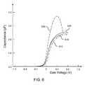
- FIG. 6is a graph showing capacitance as a function of the gate voltage for four types of metal gate electrodes.
- the present inventionrelates to a metal gate stack included in an electrode over a high-k gate dielectric, and methods of manufacturing the same, which are now described in detail with accompanying figures. It is noted that like and corresponding elements are referred to by like reference numerals. The drawings are not drawn to scale.
- an exemplary semiconductor structurecomprises a semiconductor substrate 8 and a stack of material layers formed thereupon.
- the semiconductor substrate 8contains a substrate semiconductor layer 10 and shallow trench isolation structures 12 .
- the substrate semiconductor layer 10has a semiconductor material, which may be selected from, but is not limited to, silicon, germanium, silicon-germanium alloy, silicon carbon alloy, silicon-germanium-carbon alloy, gallium arsenide, indium arsenide, indium phosphide, III-V compound semiconductor materials, II-VI compound semiconductor materials, organic semiconductor materials, and other compound semiconductor materials.
- the semiconductor material of the substrate semiconductor layer 10comprises silicon, and more typically, the semiconductor material of the substrate semiconductor layer 10 is silicon.
- the single crystalline silicon-containing semiconductor materialis preferably selected from single crystalline silicon, a single crystalline silicon carbon alloy, a single crystalline silicon germanium alloy, and a single crystalline silicon germanium carbon alloy.
- the semiconductor material of the substrate semiconductor layer 10may be appropriately doped either with p-type dopant atoms or with n-type dopant atoms.
- the dopant concentration of the substrate semiconductor layer 10may be from 1.0 ⁇ 10 15 /cm 3 to 1.0 ⁇ 10 19 /cm 3 , and typically from 1.0 ⁇ 10 16 /cm 3 to 3.0 ⁇ 10 18 /cm 3 , although lesser and greater dopant concentrations are contemplated herein also.
- the substrate semiconductor layer 10is single crystalline.
- the semiconductor substrate 8may be a bulk substrate, a semiconductor-on-insulator (SOI) substrate, or a hybrid substrate.
- SOIsemiconductor-on-insulator
- the shallow trench isolation structure 12comprises a dielectric material such as silicon oxide or silicon nitride, and is formed by methods well known in the art.
- An unpatterned chemical oxide layer 20 Lmay be formed on the exposed semiconductor surface of the substrate semiconductor layer 10 .
- An unpatterned high dielectric constant (high-k) dielectric layer 30 Lis formed directly on the top surface of the unpatterned chemical oxide layer 20 L. Even in the case the unpatterned chemical oxide layer 20 L is not formed, the deposition of the unpatterned high dielectric constant (high-k) dielectric layer 30 L and subsequent thermal processes lead to the formation of pre-existing interfacial layer between the substrate semiconductor layer 10 and the unpatterned high dielectric constant (high-k) dielectric layer 30 L
- the unpatterned chemical oxide layer 20 Lmay be formed by treatment of exposed semiconductor surfaces with a chemical.
- the process step for this wet chemical oxidationmay include treating a cleaned semiconductor surface (such as a semiconductor surface treated with hydrofluoric acid) with a mixture of ammonium hydroxide, hydrogen peroxide and water (in a 1:1:5 ratio) at 65° C.
- the chemical oxide layercan also be formed by treating the HF-last semiconductor surface in ozonated aqueous solutions, with the ozone concentration usually varying from, but not limited to: 2 parts per million (ppm) to 40 ppm
- the unpatterned chemical oxide layer 20 Lhelps minimize mobility degradation in the substrate semiconductor layer 10 due to high-k dielectric material in the unpatterned high-k dielectric layer 30 L.
- the thickness of the unpatterned chemical oxide layer 20 Lis thicker than necessary and increases the effective oxide thickness (EOT) of a composite dielectric stack, which includes the unpatterned chemical oxide layer 20 L and the unpatterned high-k dielectric layer 30 L.
- EOTeffective oxide thickness
- the scalability of EOTis severely limited by the thickness of the unpatterned chemical oxide layer 20 L.
- the substrate semiconductor layeris a silicon layer
- the unpatterned chemical oxide layer 20 Lis a silicon oxide layer.
- the thickness of the unpatterned chemical oxide layer 20 Lis from 0.1 nm to 0.4 nm, although lesser and greater thicknesses are also contemplated herein.
- a high dielectric constant (high-k) dielectric layer 30 Lis formed on a top surface of the semiconductor substrate 8 .
- the unpatterned high-k dielectric layer 30 Lcomprises a high dielectric constant (high-k) material comprising a dielectric metal oxide and having a dielectric constant that is greater than the dielectric constant of silicon nitride of 7.5.
- the unpatterned high-k dielectric layer 30 Lmay be formed by methods well known in the art including, for example, chemical vapor deposition (CVD), atomic layer deposition (ALD), molecular beam deposition (MBD), pulsed laser deposition (PLD), liquid source misted chemical deposition (LSMCD), etc.
- the dielectric metal oxidecomprises a metal and oxygen, and optionally nitrogen and/or silicon.
- Exemplary high-k dielectric materialsinclude HfO 2 , ZrO 2 , La 2 O 3 , Al 2 O 3 , TiO 2 , SrTiO 3 , LaAlO 3 , Y 2 O 3 , HfO x N y , ZrO x N y , La 2 O x N y , Al 2 O x N y , TiO x N y , SrTiO x N y , LaAlO x N y , Y 2 O x N y , a silicate thereof, and an alloy thereof.
- the thickness of the unpatterned high-k dielectric layer 30 Lmay be from 1 nm to 10 nm, and preferably from 1.5 nm to 3 nm.
- the unpatterned high-k dielectric layer 30 Lmay have an effective oxide thickness (EOT) on the order of, or less than, 1 nm.
- An unpatterned lower metal layer 40 Lis deposited directly on the top surface of the unpatterned high-k dielectric layer 30 L.
- the unpatterned lower metal layer 40 Lmay be formed, for example, by chemical vapor deposition (CVD), physical vapor deposition (PVD), or atomic layer deposition (ALD).
- CVDchemical vapor deposition
- PVDphysical vapor deposition
- ALDatomic layer deposition
- the material of the unpatterned lower metal layer 40 Lis herein referred to as a “first metallic compound” which may be a conductive transition metal nitride or a conductive transition metal carbide.
- the first metallic compoundis a compound of a first metallic element selected from transition metals and a non-metallic element. If the non-metallic element is nitrogen, the first metallic compound is a transition metal nitride. If the non-metallic element is carbon, the first metallic compound is a transition metal carbide.
- the first metallic compoundmay be selected from TiN, TiC, TaN, TaC, and a combination thereof.
- transition metalsinclude elements from Group 3B, 4B, 5B, 6B, 7B, 8B, 1B, and 2B and Lanthanides and Actinides in the Periodic Table of the Elements.
- the thickness of the unpatterned lower metal layer 40 Lmay be from 1 nm to 10 nm, and preferably from 3 nm to 10 nm, although lesser and greater thicknesses are also contemplated herein.
- An unpatterned scavenging metal layer 50 Lis deposited directly on the top surface of the unpatterned lower metal layer 40 L.
- the unpatterned scavenging metal layer 50 Lmay be formed, for example, by chemical vapor deposition (CVD), physical vapor deposition (PVD), or atomic layer deposition (ALD).
- CVDchemical vapor deposition
- PVDphysical vapor deposition
- ALDatomic layer deposition
- the first exemplary semiconductor structureis transferred from a processing chamber that deposits the unpatterned lower metal layer 40 L to another processing chamber that deposits the unpatterned scavenging metal layer 50 L without breaking vacuum to prevent formation of any interfacial layer by oxidation or introduction of oxygen into the unpatterned lower metal layer 40 L.
- the material of the unpatterned scavenging metal layer 50 L“scavenges” impurity oxygen from neighboring metallic layers during subsequent processing. For the unpatterned scavenging metal layer 50 L to effectively scavenge impurity oxygen in subsequent processing steps, it is necessary that introduction of oxygen into the unpatterned scavenging metal layer 50 L is suppressed during die formation step. Further, it is necessary to select the material for the unpatterned scavenging metal layer 50 L so that the material of the unpatterned scavenging metal layer 50 L effectively scavenges impurity oxygen atoms from the unpatterned lower metal layer 40 L and an unpatterned upper metal layer 60 L to be subsequently formed.
- the unpatterned scavenging metal layer 50 Lmay include a metal in an elemental form. Typical elemental metals that may be selected for the unpatterned scavenging metal layer 50 L include, but are not limited to, Al, Be, Mg, Ca, Sr, Ba, Sc, Y, La, Ti, Zr, Hf, Dy, Lu, Er, Pr, and Ce. In one embodiment, the unpatterned scavenging metal layer 50 consists of at least one alkaline earth metal. In another embodiment, the unpatterned scavenging metal layer 50 consists of at least one transition metal. In yet another embodiment, the unpatterned scavenging metal layer 50 consists of a mixture of at least one alkaline earth metal and at least one transition metal. Preferably, the thickness of the unpatterned scavenging metal layer 50 L may be from 0.1 nm to 3.0 nm, although lesser and greater thicknesses are also contemplated herein.
- An unpatterned upper metal layer 60 Lis deposited directly on the top surface of the unpatterned scavenging metal layer 50 L.
- the unpatterned upper metal layer 60 Lmay be formed, for example, by chemical vapor deposition (CVD), physical vapor deposition (PVD), or atomic layer deposition (ALD).
- CVDchemical vapor deposition
- PVDphysical vapor deposition
- ALDatomic layer deposition
- the first exemplary semiconductor structureis transferred from the processing chamber that deposits the unpatterned scavenging metal layer 50 L to a processing chamber that deposits the unpatterned upper metal layer 60 L without breaking vacuum to prevent formation of any interfacial layer by oxidation or introduction of oxygen into the unpatterned scavenging metal layer 50 L.
- the material of the unpatterned upper metal layer 60 Lis herein referred to as a “second metallic compound” which may be a conductive transition metal nitride or a conductive transition metal carbide.
- the second metallic compoundis a compound of a second metallic element selected from transition metals and a non-metallic element. If the non-metallic element is nitrogen, the second metallic compound is a transition metal nitride. If the non-metallic element is carbon, the second metallic compound is a transition metal carbide.
- the second metallic compoundmay be selected from TiN, TiC, TaN, TaC, and a combination thereof.
- the thickness of the unpatterned upper metal layer 60 Lmay be from lower from 1 nm to 100 nm, and preferably from 3 nm to 10 nm, although lesser and greater thicknesses are also contemplated herein.
- first metallic compound and the second metallic compoundare the same material. In another case, the first metal compound and the second metal compound are different materials.
- the material for the unpatterned scavenging metal layer 50 Lis selected such that Gibbs free energy per oxygen atom for formation of an oxide for the unpatterned scavenging metal layer 50 L is equal to or more negative than Gibbs free energy per oxygen atom for formation of an oxide of the first elemental metal within the first metallic compound for the unpatterned lower metal layer 40 L. Further, the material for the unpatterned scavenging metal layer 50 L is selected such that Gibbs free energy per oxygen atom for formation of an oxide for the unpatterned scavenging metal layer 50 L is equal to or more negative than Gibbs free energy per oxygen atom for formation of an oxide of the second elemental metal within the second metallic compound for the unpatterned upper metal layer 60 L.
- the first and second metallic compoundsmay be selected from TiN, TiC, TaN, TaC, and a combination thereof.
- the unpatterned scavenging metal layer 50 Lincludes at least one of Al, Be, Mg, Ca, Sr, Ba, Sc, Y, La, Ti, Zr, Hf, Dy, Lu, Er, Pr, and Ce.
- the material for the unpatterned scavenging metal layer 50 Lis selected such that Gibbs free energy per oxygen atom for formation of an oxide for the unpatterned scavenging metal layer 50 L is more negative than Gibbs free energy per oxygen atom for formation of an oxide of the first elemental metal within the first metallic compound for the unpatterned lower metal layer 40 L. Further, the material for the unpatterned scavenging metal layer 50 L is selected such that Gibbs free energy per oxygen atom for formation of an oxide for the unpatterned scavenging metal layer 50 L is more negative than Gibbs free energy per oxygen atom for formation of an oxide of the second elemental metal within the second metallic compound for the unpatterned upper metal layer 60 L.
- each of the first metallic compound and the second metallic compoundmay be selected from TaN, TaC, and a combination thereof.
- the unpatterned scavenging metal layer 50 Lmay comprise a metal in an elemental form and selected from Al, Be, Mg, Ca, Sr, Ba, Sc, Y, La, Ti, Zr, Hf, Dy, Lu, Er, Pr, and Ce in this illustrative example.
- At least one of the first metallic compound and the second metallic compoundmay be selected from TiN, TiC, and a combination thereof.
- the unpatterned scavenging metal layer 50 Lmay include a metal in an elemental form and selected from Al, Be, Mg, Ca, Sr, Ba, Sc, Y, La, Zr, Hf, Dy, Lu, Er, Pr, and Ce in this illustrative example.
- the first metallic compound of the unpatterned lower metal layer 40 L and the second metallic compound of the unpatterned upper metal layer 60 Lare TiN and the unpatterned scavenging metal layer 50 L is an aluminum layer including aluminum in elemental metal form.
- an unpatterned polycrystalline semiconductor layer 70 Lis deposited directly on the top surface of the unpatterned upper metal layer 60 L, for example, by low pressure chemical vapor deposition (LPCVD), rapid thermal chemical vapor deposition (RTCVD), or plasma enhanced chemical vapor deposition (PECVD).
- the unpatterned polycrystalline semiconductor layer 70 Lmay comprise polysilicon, a polycrystalline silicon germanium alloy, a polycrystalline silicon carbon alloy, or a polycrystalline silicon germanium carbon alloy.
- the unpatterned polycrystalline semiconductor layer 70 Lmay be formed as a doped polycrystalline semiconductor layer through in-situ doping.
- the unpatterned polycrystalline semiconductor layer 70 Lmay be doped by ion implantation of dopant atoms after deposition of the unpatterned polycrystalline semiconductor layer 70 L and prior to patterning of a gate electrode. Yet alternately, implantation of dopant ions may be performed on a remaining portion of the unpatterned polycrystalline semiconductor layer 70 L after patterning of the gate electrode.
- the thickness of the unpatterned polycrystalline semiconductor layer 70 Lmay be from 10 nm to 300 nm, and typically from 50 nm to 100 nm, although lesser and greater thicknesses are also contemplated herein.
- Embodiments in which the unpatterned polycrystalline semiconductor layer 70 L is not formed and the stack of the unpatterned lower metal layer 40 L, unpatterned scavenging metal layer 50 L, and unpatterned upper metal layer 60 Lconstitutes a gate electrode layer.
- a photoresist layer(not shown) is applied to the top surface of the unpatterned polycrystalline semiconductor layer 70 L and lithographically patterned to form a photoresist portion 77 (See FIG. 2 ), which has the shape of a gate electrode to be subsequently formed.
- the pattern in the photoresist portion 77is transferred into the stack of the unpatterned polycrystalline semiconductor layer 70 L, the unpatterned upper metal layer 60 L, the unpatterned scavenging metal layer 50 L, the unpatterned lower metal layer 40 L, the unpatterned high-k dielectric layer 30 L, and the unpatterned chemical oxide layer 20 L.
- the pattern transfermay be effected by an anisotropic etch that employs the photoresist portion 77 as an etch mask.
- the remaining portions of the unpatterned polycrystalline semiconductor layer 70 L, the unpatterned upper metal layer 60 L, the unpatterned scavenging metal layer 50 L, the unpatterned lower metal layer 40 Lconstitute a gate electrode, which include a polycrystalline semiconductor layer 70 , an upper metal layer 60 , a scavenging metal layer 50 , and lower metal layer 40 .
- the gate electrode ( 40 , 50 , 60 , 70 )is typically patterned as a line having a width, which is the width of the lower metal layer 40 as shown in FIG. 2 and is referred to as a “gate length.”
- the gate lengthdepends on the device characteristics and may be from the lithographically printable smallest dimension to 10 microns. Typically, the gate length is from 32 nm to 1 micron, although lesser and greater gate lengths are also contemplated herein.
- the remaining portion of the unpatterned high-k dielectric layer 30 Lis herein referred to as a high-k dielectric layer 30
- the remaining portion of the unpatterned chemical oxide layer 20 Lis herein referred to as a chemical oxide layer 20
- the high-k dielectric layer 30 and the chemical oxide layer 20collectively constitute a gate dielectric ( 20 , 30 ).
- the gate dielectric ( 20 , 30 )has an effective oxide thickness (EOT) less than 1.2 nm, and may have an EOT less than 1.0 nm.
- EOTeffective oxide thickness
- the photoresist portion 77is subsequently removed, for example, by ashing.
- the sidewalls of the gate electrode ( 40 , 50 , 60 , 70 ) and the gate dielectric ( 20 , 30 )are typically substantially vertical, i.e., parallel to the surface normal of the exposed surface of the substrate semiconductor layer 10 . Further, the sidewalls of the gate electrode ( 40 , 50 , 60 , 70 ) and the gate dielectric ( 20 , 30 ) are typically substantially vertically coincident with each other.
- source and drain extension regions 18are formed by ion implantation that employs the gate electrode ( 40 , 50 , 60 , 70 ) and the gate dielectric ( 20 , 30 ) as an implantation mask.
- the source and drain extension regions 18have a doping of the opposite conductivity type of the doping of the substrate semiconductor layer 10 .
- the substrate semiconductor layer 10has a p-type doping
- the source and drain extension regions 18have an n-type doping, and vice versa.
- the dopant concentration of the source and drain extension regions 18may be from 1.0 ⁇ 10 19 /cm 3 to 1.0 ⁇ 10 21 /cm 3 , although lesser and greater dopant concentrations are contemplated herein also.
- Each of the source and drain extension regions 18abut peripheral portions of the gate dielectric ( 20 , 30 ).
- a halo implantationmay be performed at this step to introduce dopants of the same conductivity type as the doping of the substrate semiconductor layer 10 to volumes of the substrate semiconductor layer 10 located underneath peripheral portions of the gate electrode ( 40 , 50 , 60 , 70 ) and the gate dielectric ( 20 , 30 ).
- a gate spacer 80 laterally abutting the sidewalls of the gate electrode ( 40 , 50 , 60 , 70 ) and the sidewalls of the gate dielectric ( 20 , 30 )is formed, for example, by deposition of a conformal dielectric material layer followed by an anisotropic ion etching.
- the portion of the dielectric material layer that is formed directly on the sidewalls of the gate electrode ( 40 , 50 , 60 , 70 ) and the gate dielectric ( 20 , 30 )remain after the anisotropic etch to constitute a gate spacer 80 that laterally surrounds the gate electrode ( 40 , 50 , 60 , 70 ) and the gate dielectric ( 20 , 30 ).
- the gate spacer 80includes an oxygen-impermeable material such as silicon nitride.
- source and drain regions 19are formed by ion implantation that employs the gate electrode ( 40 , 50 , 60 , 70 ) and the gate spacer 80 as an implantation mask.
- the source and drain regions 19have a doping of the same conductivity type as the doping of the source and drain extension regions 18 .
- the dopant concentration of the source and drain regions 19may be from 1.0 ⁇ 10 19 /cm 3 to 1.0 ⁇ 10 21 /cm 3 , although lesser and greater dopant concentrations are contemplated herein also.
- An activation annealis thereafter performed to activate electrical dopants implanted within the source and drain extension regions 18 and the source and drain regions 19 .
- Such an activation annealis typically performed in an oxidizing ambient during which the compositional integrity of the high-k dielectric layer may be compromised in prior art semiconductor structures.
- the thickening of the chemical oxide layer 20if present, is prevented in the exemplary semiconductor structure in FIG. 4 because the scavenging metal layer 50 consumes oxygen that diffused downward from the polycrystalline semiconductor layer 70 .
- a chemical oxide layer 20is absent in the exemplary structure of the present invention, formation of an interfacial semiconductor oxide layer between the substrate semiconductor layer 10 and the high-k dielectric layer 30 is prevented by the same mechanism. Therefore, the flat band voltage of the structure including the substrate semiconductor layer 10 , the gate dielectric ( 20 , 30 ), and the lower metal gate 40 is not affected during the activation anneal or in any other thermal processing step in an oxidizing ambient.
- a metal layer(not shown) is formed over the entire exposed top surfaces of the exemplary semiconductor structure and reacted with exposed semiconductor materials to form various metal semiconductor alloy regions.
- the metal layercomprises a metal that reacts with the semiconductor material in the source and drain regions 19 and the polycrystalline semiconductor layer 70 .
- Non-limiting exemplary materials for the metal layerinclude nickel, platinum, palladium, cobalt or a combination thereof.
- the formation of the metal layermay be effected by physical vapor deposition (PVD), chemical vapor deposition (CVD), or atomic layer deposition (ALD).
- PVDphysical vapor deposition
- CVDchemical vapor deposition
- ALDatomic layer deposition
- the metal layermay be deposited in a conformal or non-conformal manner. Preferably, the metal deposition is substantially conformal.
- the exposed semiconductor surfaces in direct contact with the metal layerare metallized by reacting with the metal in the metal layer during a metallization anneal.
- the metallizationis effected by an anneal at a temperature from 350° C. to 550° C., which is typically performed in an inert gas atmosphere, e.g., He, Ar, N 2 , or forming gas.
- the annealis performed at a temperature from 400° C. to 500° C.
- a continuous heating at a constant temperature or various ramping in temperaturemay be employed.
- the metallizationmay further be effected by an additional anneal at a temperature from 400° C. to 750° C., and preferably from 500° C. to 700° C.
- etchwhich may be a wet etch.
- a typical etchant for such a wet etchemploys aqua regia.
- the metallizationforms source and drain metal semiconductor alloy regions 89 directly on each of the source and drain regions 19 . Further, a gate metal semiconductor alloy region 87 is formed directly on the top surface of the polycrystalline semiconductor layer 70 .
- a dielectric material layer 92is deposited over the entirety of the top surfaces of the exemplary semiconductor structure.
- the dielectric material layer 60comprises a dielectric material such as silicon oxide, silicon nitride, silicon oxynitride, or a combination thereof.
- the dielectric material layer 60includes a mobile ion barrier layer (not shown).
- the mobile ion barrier layertypically comprises an impervious dielectric material such as silicon nitride and directly contacts the various metal semiconductor alloy regions ( 89 , 87 ).
- the dielectric material layer 60may additionally include, for example, a spin-on-glass and/or chemical vapor deposition (CVD) oxide such as undoped silicate glass (USG), borosilicate glass (BSG), phosphosilicate glass (PSG), fluorosilicate glass (FSG), borophosphosilicate glass (BPSG), or a combination thereof.
- CVDchemical vapor deposition
- the dielectric material layer 60may comprise a low-k dielectric material having a dielectric constant less than 3.9 (the dielectric constant of silicon oxide), and preferably less than 2.5.
- exemplary low-k dielectric materialsinclude organosilicate glass (OSG) and SiLKTM.
- the dielectric material layer 60is subsequently planarized to form a substantially planar top surface.
- Source and drain contact vias 93 and a gate contact via 95are formed through the dielectric material layer 60 to provide electrical contact to the source and drain regions 19 , respectively, and to the gate electrode ( 40 , 50 , 60 , 70 ).
- the exemplary semiconductor structure in FIG. 4functions as a field effect transistor having a high-k gate dielectric and a metal gate.
- the presence of the scavenging metal layer 50 within the gate electrode ( 40 , 50 , 60 , 70 )prevents oxygen atoms that diffuse down the polycrystalline semiconductor layer 70 from passing into the lower metal layer 40 because the oxygen atoms are scavenged by the scavenging metal layer 50 . Therefore, the field effect transistor of the present invention provides a superior reliability against oxygen diffusion that may degrade or alter the device parameters of the field effect transistor.
- the amount of change in Gibbs free energy per oxygen atom during oxidation of various metalsis shown within a temperature range from 300 K to 2,200 K.
- a reaction having a more negative change in Gibbs free energy per oxygen atomcompetes with another reaction having a less negative change in Gibbs free energy per oxygen atom for a limited supply of reactants, the reaction with the more negative change in Gibbs free energy dominates the reaction and consumes a prevailing majority of the available reactants.
- oxygen atoms or oxygen molecules that diffuse through the polycrystalline semiconductor layer 70See FIG.
- elemental metalssuch as Al, Be, Mg, Ca, Sr, Ba, Sc, Y, La, Zr, Hf, Dy, Lu, Er, Pr, and Ce have more negative changes in Gibbs free energy relative to typical transition metals such as Ti and Ta. Therefore, elemental metals such as Al, Be, Mg, Ca, Sr, Ba, Sc, Y, La, Zr, Hf, Dy, Lu, Er, Pr, and Ce effectively function as the scavenging material for the scavenging metal layer 50 (See FIG. 4 ).
- a first curve 610shows the capacitance for a reference gate electrode including an 8 nm thick TiN layer and a polycrystalline semiconductor layer formed directly thereupon according to the prior art.
- a second curve 620shows the capacitance for an exemplary gate electrode according to the present invention that includes a stack, from bottom to top, of a 3.5 nm thick TiN layer as a lower metal layer, a 1.0 nm Ti layer as a scavenging metal layer, a 3.5 nm thick TiN layer an upper metal layer, and a polycrystalline semiconductor layer.
- a third curve 630shows the capacitance for another exemplary gate electrode according to the present invention that includes a stack, from bottom to top, of a 3.5 nm thick TiN layer as a lower metal layer, a 1.0 nm Al layer as a scavenging metal layer, a 3.5 nm thick TiN layer an upper metal layer, and a polycrystalline semiconductor layer.
- a fourth curve 640shows the capacitance for an counterexample gate electrode that was formed against the teaching of the instant invention by includes a stack, from bottom to top, of a 3.5 nm thick TiN layer as a lower metal layer, a 1.0 nm Ta layer as a scavenging metal layer, a 3.5 nm thick TiN layer an upper metal layer, and a polycrystalline semiconductor layer.
- Tahas less decrease in Gibbs free energy than Ti so that use of Ta as a scavenging material layer should be avoided if the lower metal layer and the upper metal layer include TiN according to the present invention.
- the structure of the counterexample gate electrodeis not desirable.
- a HfO 2 layerwas employed as a high-k dielectric layer, which was formed between a substrate semiconductor layer and each gate electrode. All four gate electrode structures were subjected to an activation anneal at a temperature about 1,000° C. in an oxidizing ambient.
- the effective capacitance achieved by the counterexample gate stacksis less than the capacitance achieved by the prior art gate stack, as demonstrated by the first curve 610 .
- the effective oxide thickness (EOT) achieved by the counterexample gate stackis greater than the EOT achieved by the prior art gate stack, providing worse performance.
- EOTeffective oxide thickness
- use of the wrong type of material that is taught away from in the present invention for a scavenging layerresulted in increase of EOT compared with the prior art reference structure that employs a single metal layer instead.
- the importance of the selection of the material for the scavenging metal layeris underscored by the counterexample.
- the scavenging metal layer 50captures oxygen atoms from above and from below, i.e, the scavenging metal layer 50 captures oxygen atoms as the oxygen atoms diffuse through the polycrystalline semiconductor layer 70 and the upper metal layer 60 in the gate electrode toward the high-k gate dielectric 30 . Because the scavenging metal layer is more prone to oxide formation than the lower metal layer 40 and the upper metal layer 50 , the oxygen atoms are consumed within the scavenging metal layer 50 and the oxygen atoms do not reach the high-k gate dielectric 30 .
- the scavenging metal layer 50actively reduces the thickness of the chemical oxide layer 20 underneath the high-k dielectric 30 as additional oxygen atoms migrate toward the chemical oxide layer 20 from below or from the side of the chemical oxide layer 20 .
- Such migrating oxygen atomsare captured by the scavenging metal layer 50 instead of being incorporated into the chemical oxide layer 20 .
- the thickness of the chemical oxide layer 20is reduced as a significant portion of the the oxygen atoms in the chemical oxide layer 20 is consumed by the scavenging metal layer 50 .
- the field effect transistormaintains a constant threshold voltage even after a high temperature anneal in oxygen ambient.
- the effective oxide thickness (EOT) of a composite gate dielectric stackis reduced, thereby enhancing the scalability of the composite gate dielectric stack and performance of the field effect transistor.
Landscapes
- Engineering & Computer Science (AREA)
- Manufacturing & Machinery (AREA)
- Physics & Mathematics (AREA)
- Composite Materials (AREA)
- Condensed Matter Physics & Semiconductors (AREA)
- General Physics & Mathematics (AREA)
- Chemical & Material Sciences (AREA)
- Computer Hardware Design (AREA)
- Microelectronics & Electronic Packaging (AREA)
- Power Engineering (AREA)
- Insulated Gate Type Field-Effect Transistor (AREA)
- Electrodes Of Semiconductors (AREA)
- Thin Film Transistor (AREA)
Abstract
Description
| TABLE 1 |
| The Gibbs free energy change at 1000 K for the reaction Si + 2/yMxOy→ 2x/yM + |
| SiO2, wherein M is the elemental metal. |
| Oxide | Li2O | Na2O | K2O | BeO | MgO | CaO | SrO | BaO |
| ΔG | +24.298 | −20.061 | −33.749 | +32.405 | +30.572 | +39.914 | +30.821 | +21.338 |
| Oxide | Sc2O3 | Y2O3 | La2O3 | Ce2O3 | CeO2 | Pr2O3 | PrO2 | Nd2O3 |
| ΔG | +123.11 | +116.82 | +98.470 | +104.95 | +36.209 | +105.76 | +13.559 | +101.69 |
| Oxide | Sm2O3 | EnO | Eu2O3 | Gd2O3 | Tb2O3 | TbO1.72 | Dy2O3 | Ho2O3 |
| ΔG | +103.94 | +33.238 | +61.901 | +101.55 | +114.76 | +38.273 | +112.44 | +118.45 |
| Oxide | Er2O3 | Tm2O3 | Yb2O3 | Lu2O3 | ThO2 | UO2 | TiO | Ti2O3 |
| ΔG | +112.03 | +116.65 | +103.83 | +116.97 | +75.513 | +43.670 | +17.749 | +35.432 |
| Oxide | TiO2 | ZrO2 | HfO2 | VO | V2O3 | VO2 | NbO | NbO2 |
| ΔG | +7.527 | +42.326 | +47.648 | −5.314 | −30.197 | −43.280 | −10.132 | −13.872 |
| Oxide | Nb2O5 | Ta2O5 | Cr2O3 | MoO2 | MoO3 | WO2 | WO2.72 | WO3 |
| ΔG | −86.228 | −52.533 | −55.275 | −76.902 | −143.78 | −77.126 | −107.20 | −121.81 |
| Oxide | MnO | Mn3O4 | Mn2O3 | TcO2 | ReO2 | FeO | Fe3O4 | Fe2O3 |
| ΔG | −12.752 | −100.60 | −94.689 | −112.91 | −126.66 | −37.774 | −160.08 | −127.47 |
| Oxide | RuO2 | OsO2 | CoO | Rh2O3 | IrO2 | NiO | PdO | Cu2O |
| ΔG | −142.27 | −147.25 | −48.041 | −235.15 | −159.47 | −51.377 | −86.066 | −64.284 |
| Oxide | CuO | ZnO | CdO | Al2O3 | Ga2O3 | In2O3 | GeO2 | SnO |
| ΔG | −71.375 | −28.461 | −49.433 | +63.399 | −79.411 | −117.72 | −82.124 | −43.514 |
| Oxide | SnO2 | PbO | Pb3O4 | PbO2 | SbO2 | Bi2O3 | TeO2 |
| ΔG | −84.977 | −59.249 | −269.62 | −155.79 | −110.52 | −191.85 | −140.95 |
Claims (25)
Priority Applications (7)
| Application Number | Priority Date | Filing Date | Title |
|---|---|---|---|
| US12/487,248US7989902B2 (en) | 2009-06-18 | 2009-06-18 | Scavenging metal stack for a high-k gate dielectric |
| KR1020100044266AKR101606210B1 (en) | 2009-06-18 | 2010-05-12 | Scavenging metal stack for a high-k gate dielectric |
| CN2010102051781ACN101930996B (en) | 2009-06-18 | 2010-06-13 | Semiconductor structure and forming method thereof |
| JP2010136861AJP5811432B2 (en) | 2009-06-18 | 2010-06-16 | Semiconductor structure for trapping impurity oxygen for high-k gate dielectric and method for forming the structure (trapping metal stack for high-k gate dielectric) |
| US13/099,790US8367496B2 (en) | 2009-06-18 | 2011-05-03 | Scavanging metal stack for a high-k gate dielectric |
| US13/630,235US9105745B2 (en) | 2009-06-18 | 2012-09-28 | Fabrication of low threshold voltage and inversion oxide thickness scaling for a high-k metal gate p-type MOSFET |
| US14/699,264US20150243662A1 (en) | 2009-06-18 | 2015-04-29 | Low Threshold Voltage and Inversion Oxide Thickness Scaling for a High-K Metal Gate P-Type MOSFET |
Applications Claiming Priority (1)
| Application Number | Priority Date | Filing Date | Title |
|---|---|---|---|
| US12/487,248US7989902B2 (en) | 2009-06-18 | 2009-06-18 | Scavenging metal stack for a high-k gate dielectric |
Related Child Applications (1)
| Application Number | Title | Priority Date | Filing Date |
|---|---|---|---|
| US13/099,790DivisionUS8367496B2 (en) | 2009-06-18 | 2011-05-03 | Scavanging metal stack for a high-k gate dielectric |
Publications (2)
| Publication Number | Publication Date |
|---|---|
| US20100320547A1 US20100320547A1 (en) | 2010-12-23 |
| US7989902B2true US7989902B2 (en) | 2011-08-02 |
Family
ID=43353519
Family Applications (2)
| Application Number | Title | Priority Date | Filing Date |
|---|---|---|---|
| US12/487,248Active2029-07-11US7989902B2 (en) | 2009-06-18 | 2009-06-18 | Scavenging metal stack for a high-k gate dielectric |
| US13/099,790ActiveUS8367496B2 (en) | 2009-06-18 | 2011-05-03 | Scavanging metal stack for a high-k gate dielectric |
Family Applications After (1)
| Application Number | Title | Priority Date | Filing Date |
|---|---|---|---|
| US13/099,790ActiveUS8367496B2 (en) | 2009-06-18 | 2011-05-03 | Scavanging metal stack for a high-k gate dielectric |
Country Status (4)
| Country | Link |
|---|---|
| US (2) | US7989902B2 (en) |
| JP (1) | JP5811432B2 (en) |
| KR (1) | KR101606210B1 (en) |
| CN (1) | CN101930996B (en) |
Cited By (21)
| Publication number | Priority date | Publication date | Assignee | Title |
|---|---|---|---|---|
| US20110298053A1 (en)* | 2010-06-03 | 2011-12-08 | Institute of Microelectronics, Chinese Academy of Sciences | Manufacturing method of gate stack and semiconductor device |
| US8541867B2 (en) | 2011-06-28 | 2013-09-24 | International Business Machines Corporation | Metal insulator metal structure with remote oxygen scavenging |
| US20140004674A1 (en)* | 2012-06-28 | 2014-01-02 | International Business Machines Corporation | Reducing the inversion oxide thickness of a high-k stack fabricated on high mobility semiconductor material |
| US8716088B2 (en) | 2012-06-27 | 2014-05-06 | International Business Machines Corporation | Scavenging metal stack for a high-K gate dielectric |
| US8772116B2 (en) | 2012-11-20 | 2014-07-08 | International Business Machines Corporation | Dielectric equivalent thickness and capacitance scaling for semiconductor devices |
| US20140246734A1 (en)* | 2013-03-01 | 2014-09-04 | Globalfoundries Inc. | Replacement metal gate with mulitiple titanium nitride laters |
| US8900952B2 (en)* | 2013-03-11 | 2014-12-02 | International Business Machines Corporation | Gate stack including a high-k gate dielectric that is optimized for low voltage applications |
| US8912061B2 (en) | 2011-06-28 | 2014-12-16 | International Business Machines Corporation | Floating gate device with oxygen scavenging element |
| US9093495B2 (en) | 2012-01-03 | 2015-07-28 | International Business Machines Corporation | Method and structure to reduce FET threshold voltage shift due to oxygen diffusion |
| US9099336B2 (en) | 2013-02-25 | 2015-08-04 | Samsung Electronics Co., Ltd. | Semiconductor device and fabricating method thereof |
| US9257349B2 (en) | 2011-09-22 | 2016-02-09 | Taiwan Semiconductor Manufacturing Company, Ltd. | Method of scavenging impurities in forming a gate stack having an interfacial layer |
| US9443910B1 (en) | 2015-07-09 | 2016-09-13 | Sandisk Technologies Llc | Silicided bit line for reversible-resistivity memory |
| US9647094B2 (en) | 2013-08-02 | 2017-05-09 | University Of Kentucky Research Foundation | Method of manufacturing a semiconductor heteroepitaxy structure |
| US9653462B2 (en) | 2014-12-26 | 2017-05-16 | Samsung Electronics Co., Ltd. | Semiconductor device and method for fabricating the same |
| US9711399B2 (en) | 2013-12-26 | 2017-07-18 | Intel Corporation | Direct plasma densification process and semiconductor devices |
| US9947668B2 (en) | 2014-04-21 | 2018-04-17 | Samsung Electronics Co., Ltd. | Semiconductor devices and methods of forming the same |
| US10096513B2 (en) | 2013-12-26 | 2018-10-09 | Intel Corporation | Direct plasma densification process and semiconductor devices |
| US11121259B2 (en) | 2019-07-17 | 2021-09-14 | International Business Machines Corporation | Metal-oxide-based neuromorphic device |
| US11568927B2 (en) | 2021-03-30 | 2023-01-31 | International Business Machines Corporation | Two-terminal non-volatile memory cell for decoupled read and write operations |
| US11569444B2 (en) | 2021-03-30 | 2023-01-31 | International Business Machines Corporation | Three-dimensional confined memory cell with decoupled read-write |
| US12369330B2 (en) | 2021-11-19 | 2025-07-22 | International Business Machines Corporation | Self-aligned crossbar-compatible electrochemical memory structure |
Families Citing this family (46)
| Publication number | Priority date | Publication date | Assignee | Title |
|---|---|---|---|---|
| US20130032886A1 (en) | 2011-08-01 | 2013-02-07 | International Business Machines Corporation | Low Threshold Voltage And Inversion Oxide Thickness Scaling For A High-K Metal Gate P-Type MOSFET |
| US8437174B2 (en) | 2010-02-15 | 2013-05-07 | Micron Technology, Inc. | Memcapacitor devices, field effect transistor devices, non-volatile memory arrays, and methods of programming |
| US8416609B2 (en) | 2010-02-15 | 2013-04-09 | Micron Technology, Inc. | Cross-point memory cells, non-volatile memory arrays, methods of reading a memory cell, methods of programming a memory cell, methods of writing to and reading from a memory cell, and computer systems |
| US8343839B2 (en) | 2010-05-27 | 2013-01-01 | International Business Machines Corporation | Scaled equivalent oxide thickness for field effect transistor devices |
| US8634224B2 (en) | 2010-08-12 | 2014-01-21 | Micron Technology, Inc. | Memory cells, non-volatile memory arrays, methods of operating memory cells, methods of writing to and reading from a memory cell, and methods of programming a memory cell |
| FR2965661A1 (en)* | 2010-10-04 | 2012-04-06 | St Microelectronics Crolles 2 | METHOD FOR MANUFACTURING MOS TRANSISTORS WITH DIFFERENT TYPES OF GRID STACKS |
| JP5626010B2 (en)* | 2011-02-25 | 2014-11-19 | 富士通株式会社 | Semiconductor device, manufacturing method thereof, and power supply device |
| CN102651313B (en)* | 2011-02-25 | 2014-12-24 | 中国科学院微电子研究所 | Preparation of PMOS device laminated structure and gate work function adjusting method |
| US20120280288A1 (en) | 2011-05-04 | 2012-11-08 | International Business Machines Corporation | Inversion thickness reduction in high-k gate stacks formed by replacement gate processes |
| US8860143B2 (en) | 2011-05-16 | 2014-10-14 | Tsinghua University | High-K gate dielectric with work function adjustment metal layer |
| WO2012155392A1 (en)* | 2011-05-16 | 2012-11-22 | Tsinghua University | Semiconductor structure and method for forming the same |
| US9396946B2 (en)* | 2011-06-27 | 2016-07-19 | Cree, Inc. | Wet chemistry processes for fabricating a semiconductor device with increased channel mobility |
| US8440520B2 (en) | 2011-08-23 | 2013-05-14 | Tokyo Electron Limited | Diffused cap layers for modifying high-k gate dielectrics and interface layers |
| US8597995B2 (en)* | 2011-09-24 | 2013-12-03 | Taiwan Semiconductor Manufacturing Company, Ltd. | Metal gate device with low temperature oxygen scavenging |
| US9059211B2 (en)* | 2011-10-03 | 2015-06-16 | International Business Machines Corporation | Oxygen scavenging spacer for a gate electrode |
| US8633118B2 (en) | 2012-02-01 | 2014-01-21 | Tokyo Electron Limited | Method of forming thin metal and semi-metal layers by thermal remote oxygen scavenging |
| US8865538B2 (en) | 2012-03-30 | 2014-10-21 | Tokyo Electron Limited | Method of integrating buried threshold voltage adjustment layers for CMOS processing |
| JP5960491B2 (en)* | 2012-04-27 | 2016-08-02 | キヤノンアネルバ株式会社 | Semiconductor device and manufacturing method thereof |
| CN102779852B (en)* | 2012-07-18 | 2014-09-10 | 电子科技大学 | SiC vertical double diffusion metal oxide semiconductor structure (VDMOS) device with composite gate dielectric structure |
| US8836037B2 (en)* | 2012-08-13 | 2014-09-16 | International Business Machines Corporation | Structure and method to form input/output devices |
| US8865581B2 (en) | 2012-10-19 | 2014-10-21 | Tokyo Electron Limited | Hybrid gate last integration scheme for multi-layer high-k gate stacks |
| US9190409B2 (en) | 2013-02-25 | 2015-11-17 | Renesas Electronics Corporation | Replacement metal gate transistor with controlled threshold voltage |
| US8802527B1 (en)* | 2013-03-15 | 2014-08-12 | International Business Machines Corporation | Gate electrode optimized for low voltage operation |
| US8981332B2 (en) | 2013-03-15 | 2015-03-17 | Intermolecular, Inc. | Nonvolatile resistive memory element with an oxygen-gettering layer |
| US20160064285A1 (en)* | 2013-03-27 | 2016-03-03 | Ps4 Luxco S.A.R.L.) | Manufacturing method for semiconductor device |
| FR3005201A1 (en) | 2013-04-24 | 2014-10-31 | St Microelectronics Crolles 2 | METHOD FOR MAKING A METAL GRID MOS TRANSISTOR, ESPECIALLY A PMOS TRANSISTOR, AND CORRESPONDING INTEGRATED CIRCUIT |
| CN104134691B (en)* | 2013-05-03 | 2017-09-08 | 中国科学院微电子研究所 | Semiconductor device and method for manufacturing the same |
| KR20140139340A (en)* | 2013-05-27 | 2014-12-05 | 삼성전자주식회사 | Semiconductor device and method for fabricating the same |
| KR102099881B1 (en)* | 2013-09-03 | 2020-05-15 | 삼성전자 주식회사 | Semiconductor device and method of fabricating the same |
| US9231098B2 (en)* | 2013-10-30 | 2016-01-05 | Taiwan Semiconductor Manufacturing Co., Ltd. | Mechanism for forming metal gate structure |
| KR102084657B1 (en)* | 2013-11-04 | 2020-03-04 | 에스케이하이닉스 주식회사 | Method and gate ructure for threshold voltage modulation in transistors |
| US9349823B2 (en)* | 2013-11-14 | 2016-05-24 | GlobalFoundries, Inc. | Methods of scaling thickness of a gate dielectric structure, methods of forming an integrated circuit, and integrated circuits |
| US9449827B2 (en) | 2014-02-04 | 2016-09-20 | International Business Machines Corporation | Metal semiconductor alloy contact resistance improvement |
| US9379214B2 (en)* | 2014-02-14 | 2016-06-28 | Semi Solutions Llc | Reduced variation MOSFET using a drain-extension-last process |
| CN105206531B (en)* | 2014-06-30 | 2018-08-10 | 中芯国际集成电路制造(上海)有限公司 | Transistor and forming method thereof |
| JP6194516B2 (en) | 2014-08-29 | 2017-09-13 | 豊田合成株式会社 | MIS type semiconductor device |
| KR102342850B1 (en)* | 2015-04-17 | 2021-12-23 | 삼성전자주식회사 | Curing method of dielectric layer for manufacturing semiconductor device |
| JP6367152B2 (en) | 2015-06-08 | 2018-08-01 | 東芝メモリ株式会社 | Storage device |
| US9595593B2 (en)* | 2015-06-29 | 2017-03-14 | Taiwan Semiconductor Manufacturing Co., Ltd. | Semiconductor structure with interfacial layer and method for manufacturing the same |
| US9865703B2 (en) | 2015-12-31 | 2018-01-09 | International Business Machines Corporation | High-K layer chamfering to prevent oxygen ingress in replacement metal gate (RMG) process |
| US9559016B1 (en)* | 2016-01-15 | 2017-01-31 | International Business Machines Corporation | Semiconductor device having a gate stack with tunable work function |
| US9583400B1 (en)* | 2016-01-15 | 2017-02-28 | International Business Machines Corporation | Gate stack with tunable work function |
| US9793397B1 (en)* | 2016-09-23 | 2017-10-17 | International Business Machines Corporation | Ferroelectric gate dielectric with scaled interfacial layer for steep sub-threshold slope field-effect transistor |
| CN117397386A (en)* | 2021-04-21 | 2024-01-12 | 无锡舜铭存储科技有限公司 | Ferroelectric memory and method for manufacturing the same |
| CN113956033B (en)* | 2021-12-06 | 2023-05-02 | 武汉理工大学 | Medium high Q value microwave dielectric ceramic and preparation method thereof |
| KR102603515B1 (en)* | 2022-11-03 | 2023-11-20 | (주)이큐테크플러스 | Method for forming improved interfaces and thin films using high-density radicals |
Citations (2)
| Publication number | Priority date | Publication date | Assignee | Title |
|---|---|---|---|---|
| US20040185198A1 (en)* | 2003-01-31 | 2004-09-23 | Sisson Edwin A. | Oxygen-scavenging articles devoid of visual spots upon oxidation and related methods |
| US20100187643A1 (en)* | 2009-01-26 | 2010-07-29 | International Business Machines Corporation | Method for tuning the threshold voltage of a metal gate and high-k device |
Family Cites Families (17)
| Publication number | Priority date | Publication date | Assignee | Title |
|---|---|---|---|---|
| JP3724915B2 (en)* | 1997-05-15 | 2005-12-07 | パイオニア株式会社 | Electron emission device and display device using the same |
| US6228277B1 (en)* | 1998-10-14 | 2001-05-08 | Lucent Technologies Inc. | Etch endpoint detection |
| US6066884A (en)* | 1999-03-19 | 2000-05-23 | Lucent Technologies Inc. | Schottky diode guard ring structures |
| JP2001352054A (en)* | 2000-06-02 | 2001-12-21 | Hitachi Ltd | Semiconductor device and manufacturing method thereof |
| JP4415528B2 (en) | 2002-05-07 | 2010-02-17 | 株式会社日立製作所 | Manufacturing method of semiconductor device |
| US7667277B2 (en)* | 2005-01-13 | 2010-02-23 | International Business Machines Corporation | TiC as a thermally stable p-metal carbide on high k SiO2 gate stacks |
| US7598545B2 (en)* | 2005-04-21 | 2009-10-06 | International Business Machines Corporation | Using metal/metal nitride bilayers as gate electrodes in self-aligned aggressively scaled CMOS devices |
| JP4602214B2 (en)* | 2005-10-03 | 2010-12-22 | 富士通セミコンダクター株式会社 | Semiconductor device and manufacturing method thereof |
| US7226831B1 (en)* | 2005-12-27 | 2007-06-05 | Intel Corporation | Device with scavenging spacer layer |
| US20070152276A1 (en)* | 2005-12-30 | 2007-07-05 | International Business Machines Corporation | High performance CMOS circuits, and methods for fabricating the same |
| US7510956B2 (en)* | 2006-01-30 | 2009-03-31 | Fressscale Semiconductor, Inc. | MOS device with multi-layer gate stack |
| US20070178634A1 (en) | 2006-01-31 | 2007-08-02 | Hyung Suk Jung | Cmos semiconductor devices having dual work function metal gate stacks |
| KR100662850B1 (en) | 2006-02-02 | 2007-01-02 | 삼성전자주식회사 | Semiconductor device in which a plurality of metal layers are stacked |
| JP2007266230A (en)* | 2006-03-28 | 2007-10-11 | Toshiba Corp | Semiconductor device and manufacturing method thereof |
| JP4459257B2 (en)* | 2007-06-27 | 2010-04-28 | 株式会社東芝 | Semiconductor device |
| JP5139023B2 (en)* | 2007-10-16 | 2013-02-06 | 株式会社東芝 | Manufacturing method of semiconductor device |
| JP5194732B2 (en)* | 2007-11-16 | 2013-05-08 | 富士通株式会社 | Semiconductor device manufacturing method and semiconductor device |
- 2009
- 2009-06-18USUS12/487,248patent/US7989902B2/enactiveActive
- 2010
- 2010-05-12KRKR1020100044266Apatent/KR101606210B1/ennot_activeExpired - Fee Related
- 2010-06-13CNCN2010102051781Apatent/CN101930996B/ennot_activeExpired - Fee Related
- 2010-06-16JPJP2010136861Apatent/JP5811432B2/ennot_activeExpired - Fee Related
- 2011
- 2011-05-03USUS13/099,790patent/US8367496B2/enactiveActive
Patent Citations (2)
| Publication number | Priority date | Publication date | Assignee | Title |
|---|---|---|---|---|
| US20040185198A1 (en)* | 2003-01-31 | 2004-09-23 | Sisson Edwin A. | Oxygen-scavenging articles devoid of visual spots upon oxidation and related methods |
| US20100187643A1 (en)* | 2009-01-26 | 2010-07-29 | International Business Machines Corporation | Method for tuning the threshold voltage of a metal gate and high-k device |
Non-Patent Citations (1)
| Title |
|---|
| Hubbard et al., "Thermodynamic stability of binary oxides in contact with silicon", J. Mater. Res. vol. 11, No. 11, Nov. 1996, pp. 2757-2776. |
Cited By (28)
| Publication number | Priority date | Publication date | Assignee | Title |
|---|---|---|---|---|
| US8716095B2 (en)* | 2010-06-03 | 2014-05-06 | Institute of Microelectronics, Chinese Academy of Sciences | Manufacturing method of gate stack and semiconductor device |
| US20110298053A1 (en)* | 2010-06-03 | 2011-12-08 | Institute of Microelectronics, Chinese Academy of Sciences | Manufacturing method of gate stack and semiconductor device |
| US8541867B2 (en) | 2011-06-28 | 2013-09-24 | International Business Machines Corporation | Metal insulator metal structure with remote oxygen scavenging |
| US8941169B2 (en) | 2011-06-28 | 2015-01-27 | International Business Machines Corporation | Floating gate device with oxygen scavenging element |
| US8912061B2 (en) | 2011-06-28 | 2014-12-16 | International Business Machines Corporation | Floating gate device with oxygen scavenging element |
| US9257349B2 (en) | 2011-09-22 | 2016-02-09 | Taiwan Semiconductor Manufacturing Company, Ltd. | Method of scavenging impurities in forming a gate stack having an interfacial layer |
| US9093495B2 (en) | 2012-01-03 | 2015-07-28 | International Business Machines Corporation | Method and structure to reduce FET threshold voltage shift due to oxygen diffusion |
| US9431289B2 (en) | 2012-01-03 | 2016-08-30 | Globalfoundries Inc. | Method and structure to reduce FET threshold voltage shift due to oxygen diffusion |
| US8716088B2 (en) | 2012-06-27 | 2014-05-06 | International Business Machines Corporation | Scavenging metal stack for a high-K gate dielectric |
| US8735996B2 (en) | 2012-06-27 | 2014-05-27 | International Business Machines Corporation | Scavenging metal stack for a high-K gate dielectric |
| US20140001516A1 (en)* | 2012-06-28 | 2014-01-02 | International Business Machines Corporation | Reducing the inversion oxide thickness of a high-k stack fabricated on high mobility semiconductor material |
| US8865551B2 (en)* | 2012-06-28 | 2014-10-21 | International Business Machines Corporation | Reducing the inversion oxide thickness of a high-k stack fabricated on high mobility semiconductor material |
| US8853751B2 (en)* | 2012-06-28 | 2014-10-07 | International Business Machines Corporation | Reducing the inversion oxide thickness of a high-K stack fabricated on high mobility semiconductor material |
| US20140004674A1 (en)* | 2012-06-28 | 2014-01-02 | International Business Machines Corporation | Reducing the inversion oxide thickness of a high-k stack fabricated on high mobility semiconductor material |
| US8772116B2 (en) | 2012-11-20 | 2014-07-08 | International Business Machines Corporation | Dielectric equivalent thickness and capacitance scaling for semiconductor devices |
| US9099336B2 (en) | 2013-02-25 | 2015-08-04 | Samsung Electronics Co., Ltd. | Semiconductor device and fabricating method thereof |
| US20140246734A1 (en)* | 2013-03-01 | 2014-09-04 | Globalfoundries Inc. | Replacement metal gate with mulitiple titanium nitride laters |
| US8900952B2 (en)* | 2013-03-11 | 2014-12-02 | International Business Machines Corporation | Gate stack including a high-k gate dielectric that is optimized for low voltage applications |
| US9647094B2 (en) | 2013-08-02 | 2017-05-09 | University Of Kentucky Research Foundation | Method of manufacturing a semiconductor heteroepitaxy structure |
| US10096513B2 (en) | 2013-12-26 | 2018-10-09 | Intel Corporation | Direct plasma densification process and semiconductor devices |
| US9711399B2 (en) | 2013-12-26 | 2017-07-18 | Intel Corporation | Direct plasma densification process and semiconductor devices |
| US9947668B2 (en) | 2014-04-21 | 2018-04-17 | Samsung Electronics Co., Ltd. | Semiconductor devices and methods of forming the same |
| US9653462B2 (en) | 2014-12-26 | 2017-05-16 | Samsung Electronics Co., Ltd. | Semiconductor device and method for fabricating the same |
| US9443910B1 (en) | 2015-07-09 | 2016-09-13 | Sandisk Technologies Llc | Silicided bit line for reversible-resistivity memory |
| US11121259B2 (en) | 2019-07-17 | 2021-09-14 | International Business Machines Corporation | Metal-oxide-based neuromorphic device |
| US11568927B2 (en) | 2021-03-30 | 2023-01-31 | International Business Machines Corporation | Two-terminal non-volatile memory cell for decoupled read and write operations |
| US11569444B2 (en) | 2021-03-30 | 2023-01-31 | International Business Machines Corporation | Three-dimensional confined memory cell with decoupled read-write |
| US12369330B2 (en) | 2021-11-19 | 2025-07-22 | International Business Machines Corporation | Self-aligned crossbar-compatible electrochemical memory structure |
Also Published As
| Publication number | Publication date |
|---|---|
| US20100320547A1 (en) | 2010-12-23 |
| JP2011003899A (en) | 2011-01-06 |
| US8367496B2 (en) | 2013-02-05 |
| US20110207280A1 (en) | 2011-08-25 |
| CN101930996A (en) | 2010-12-29 |
| CN101930996B (en) | 2012-09-05 |
| JP5811432B2 (en) | 2015-11-11 |
| KR20100136406A (en) | 2010-12-28 |
| KR101606210B1 (en) | 2016-03-24 |
Similar Documents
| Publication | Publication Date | Title |
|---|---|---|
| US7989902B2 (en) | Scavenging metal stack for a high-k gate dielectric | |
| US9105745B2 (en) | Fabrication of low threshold voltage and inversion oxide thickness scaling for a high-k metal gate p-type MOSFET | |
| US8716088B2 (en) | Scavenging metal stack for a high-K gate dielectric | |
| US8778759B1 (en) | Gate electrode optimized for low voltage operation | |
| US7709902B2 (en) | Metal gate CMOS with at least a single gate metal and dual gate dielectrics | |
| US7682917B2 (en) | Disposable metallic or semiconductor gate spacer | |
| US7872317B2 (en) | Dual metal gate self-aligned integration | |
| US8304836B2 (en) | Structure and method to obtain EOT scaled dielectric stacks | |
| US20090108294A1 (en) | Scalable high-k dielectric gate stack | |
| US20110193181A1 (en) | Semiconductor device having different metal gate structures | |
| US8716118B2 (en) | Replacement gate structure for transistor with a high-K gate stack | |
| KR20010053230A (en) | ULSI MOS with high dielectric constant gate insulator | |
| US20090206416A1 (en) | Dual metal gate structures and methods | |
| US20200006157A1 (en) | Method for Patterning a Lanthanum Containing Layer | |
| US20130032897A1 (en) | Mosfet gate electrode employing arsenic-doped silicon-germanium alloy layer | |
| KR100843223B1 (en) | Semiconductor device adopting heterogeneous metal gate structure according to channel type and its manufacturing method | |
| US8853751B2 (en) | Reducing the inversion oxide thickness of a high-K stack fabricated on high mobility semiconductor material | |
| CN114446880A (en) | Semiconductor device and method for forming the same | |
| KR100843230B1 (en) | A semiconductor device having a gate electrode having a metal layer and a manufacturing method thereof | |
| US20050260817A1 (en) | Semiconductor device and method for manufacturing the same | |
| JP3779556B2 (en) | Field effect transistor | |
| KR20080018711A (en) | Semiconductor device and manufacturing method thereof | |
| US20080142903A1 (en) | Semiconductor device and method for manufacturing the same |
Legal Events
| Date | Code | Title | Description |
|---|---|---|---|
| AS | Assignment | Owner name:INTERNATIONAL BUSINESS MACHINES CORPORATION, NEW Y Free format text:ASSIGNMENT OF ASSIGNORS INTEREST;ASSIGNORS:ANDO, TAKASHI;CHOI, CHANGHWAN;FRANK, MARTIN M.;AND OTHERS;REEL/FRAME:022844/0798 Effective date:20090115 | |
| STCF | Information on status: patent grant | Free format text:PATENTED CASE | |
| FPAY | Fee payment | Year of fee payment:4 | |
| AS | Assignment | Owner name:GLOBALFOUNDRIES U.S. 2 LLC, NEW YORK Free format text:ASSIGNMENT OF ASSIGNORS INTEREST;ASSIGNOR:INTERNATIONAL BUSINESS MACHINES CORPORATION;REEL/FRAME:036550/0001 Effective date:20150629 | |
| AS | Assignment | Owner name:GLOBALFOUNDRIES INC., CAYMAN ISLANDS Free format text:ASSIGNMENT OF ASSIGNORS INTEREST;ASSIGNORS:GLOBALFOUNDRIES U.S. 2 LLC;GLOBALFOUNDRIES U.S. INC.;REEL/FRAME:036779/0001 Effective date:20150910 | |
| AS | Assignment | Owner name:WILMINGTON TRUST, NATIONAL ASSOCIATION, DELAWARE Free format text:SECURITY AGREEMENT;ASSIGNOR:GLOBALFOUNDRIES INC.;REEL/FRAME:049490/0001 Effective date:20181127 | |
| MAFP | Maintenance fee payment | Free format text:PAYMENT OF MAINTENANCE FEE, 8TH YEAR, LARGE ENTITY (ORIGINAL EVENT CODE: M1552); ENTITY STATUS OF PATENT OWNER: LARGE ENTITY Year of fee payment:8 | |
| AS | Assignment | Owner name:GLOBALFOUNDRIES U.S. INC., CALIFORNIA Free format text:ASSIGNMENT OF ASSIGNORS INTEREST;ASSIGNOR:GLOBALFOUNDRIES INC.;REEL/FRAME:054633/0001 Effective date:20201022 | |
| AS | Assignment | Owner name:GLOBALFOUNDRIES INC., CAYMAN ISLANDS Free format text:RELEASE BY SECURED PARTY;ASSIGNOR:WILMINGTON TRUST, NATIONAL ASSOCIATION;REEL/FRAME:054636/0001 Effective date:20201117 | |
| AS | Assignment | Owner name:GLOBALFOUNDRIES U.S. INC., NEW YORK Free format text:RELEASE BY SECURED PARTY;ASSIGNOR:WILMINGTON TRUST, NATIONAL ASSOCIATION;REEL/FRAME:056987/0001 Effective date:20201117 | |
| MAFP | Maintenance fee payment | Free format text:PAYMENT OF MAINTENANCE FEE, 12TH YEAR, LARGE ENTITY (ORIGINAL EVENT CODE: M1553); ENTITY STATUS OF PATENT OWNER: LARGE ENTITY Year of fee payment:12 |