US7989865B2 - Deep trench capacitor for SOI CMOS devices for soft error immunity - Google Patents
Deep trench capacitor for SOI CMOS devices for soft error immunityDownload PDFInfo
- Publication number
- US7989865B2 US7989865B2US12/200,538US20053808AUS7989865B2US 7989865 B2US7989865 B2US 7989865B2US 20053808 AUS20053808 AUS 20053808AUS 7989865 B2US7989865 B2US 7989865B2
- Authority
- US
- United States
- Prior art keywords
- semiconductor
- deep trench
- trench capacitor
- channel region
- layer
- Prior art date
- Legal status (The legal status is an assumption and is not a legal conclusion. Google has not performed a legal analysis and makes no representation as to the accuracy of the status listed.)
- Active
Links
Images


Classifications
- H—ELECTRICITY
- H10—SEMICONDUCTOR DEVICES; ELECTRIC SOLID-STATE DEVICES NOT OTHERWISE PROVIDED FOR
- H10D—INORGANIC ELECTRIC SEMICONDUCTOR DEVICES
- H10D86/00—Integrated devices formed in or on insulating or conducting substrates, e.g. formed in silicon-on-insulator [SOI] substrates or on stainless steel or glass substrates
- H10D86/201—Integrated devices formed in or on insulating or conducting substrates, e.g. formed in silicon-on-insulator [SOI] substrates or on stainless steel or glass substrates the substrates comprising an insulating layer on a semiconductor body, e.g. SOI
- H—ELECTRICITY
- H10—SEMICONDUCTOR DEVICES; ELECTRIC SOLID-STATE DEVICES NOT OTHERWISE PROVIDED FOR
- H10B—ELECTRONIC MEMORY DEVICES
- H10B12/00—Dynamic random access memory [DRAM] devices
- H10B12/01—Manufacture or treatment
- H10B12/02—Manufacture or treatment for one transistor one-capacitor [1T-1C] memory cells
- H10B12/03—Making the capacitor or connections thereto
- H10B12/038—Making the capacitor or connections thereto the capacitor being in a trench in the substrate
- H—ELECTRICITY
- H10—SEMICONDUCTOR DEVICES; ELECTRIC SOLID-STATE DEVICES NOT OTHERWISE PROVIDED FOR
- H10D—INORGANIC ELECTRIC SEMICONDUCTOR DEVICES
- H10D1/00—Resistors, capacitors or inductors
- H10D1/01—Manufacture or treatment
- H10D1/045—Manufacture or treatment of capacitors having potential barriers, e.g. varactors
- H10D1/047—Manufacture or treatment of capacitors having potential barriers, e.g. varactors of conductor-insulator-semiconductor capacitors, e.g. trench capacitors
- H—ELECTRICITY
- H10—SEMICONDUCTOR DEVICES; ELECTRIC SOLID-STATE DEVICES NOT OTHERWISE PROVIDED FOR
- H10D—INORGANIC ELECTRIC SEMICONDUCTOR DEVICES
- H10D84/00—Integrated devices formed in or on semiconductor substrates that comprise only semiconducting layers, e.g. on Si wafers or on GaAs-on-Si wafers
- H10D84/80—Integrated devices formed in or on semiconductor substrates that comprise only semiconducting layers, e.g. on Si wafers or on GaAs-on-Si wafers characterised by the integration of at least one component covered by groups H10D12/00 or H10D30/00, e.g. integration of IGFETs
- H10D84/811—Combinations of field-effect devices and one or more diodes, capacitors or resistors
- H—ELECTRICITY
- H10—SEMICONDUCTOR DEVICES; ELECTRIC SOLID-STATE DEVICES NOT OTHERWISE PROVIDED FOR
- H10D—INORGANIC ELECTRIC SEMICONDUCTOR DEVICES
- H10D86/00—Integrated devices formed in or on insulating or conducting substrates, e.g. formed in silicon-on-insulator [SOI] substrates or on stainless steel or glass substrates
- H10D86/01—Manufacture or treatment
Definitions
- the present inventionrelates to complimentary metal oxide semiconductor (CMOS) structures, and more specifically, to a semiconductor structure that incorporates a capacitor within the structure for reducing the soft error rate (SER) of a circuit.
- CMOScomplimentary metal oxide semiconductor
- SERsoft error rate
- a semiconductor structureincludes an active semiconductor layer, a semiconductor device having a gate disposed on top of the active semiconductor layer, and source and drain regions and a body/channel region disposed within the active semiconductor layer, an insulator layer having a first and second side, the first side being adjacent to the active semiconductor layer, a substrate disposed adjacent to the second side of the insulator layer, a deep trench capacitor disposed under the body/channel region of the semiconductor device.
- the deep trench capacitorelectrically connects with and contacts the body/channel region of the semiconductor device, and is located adjacent to the gate of the semiconductor device.
- a semiconductor structurewhich includes an active semiconductor layer, an insulator layer having a first and second side, the first side being adjacent to the active semiconductor layer, a substrate disposed adjacent to the second side of the insulator layer, a plurality of semiconductor devices, each semiconductor device including a gate disposed on top of the active semiconductor layer, and source and drain regions and a body/channel region disposed within the active semiconductor layer, and a deep trench capacitor disposed under the body/channel regions of the semiconductor devices.
- the deep trench capacitorelectrically connects with and contacts the body/channel regions.
- a semiconductor structurein yet another embodiment, includes an active semiconductor layer, an insulator layer having a first and second side, the first side being adjacent to the active semiconductor layer, a substrate disposed adjacent to the second side of the insulator layer, a plurality of semiconductor devices, each semiconductor device including source and drain regions and a body/channel region disposed within the active semiconductor layer, and sharing a common gate disposed on top of the active semiconductor layer, and a deep trench capacitor disposed under the body/channel regions of the semiconductor devices.
- the deep trench capacitorelectrically connects with and contacts the body/channel regions.
- a method of forming semiconductor structureincludes forming a substrate, forming an insulating layer on top of the substrate, forming an active semiconductor layer on top of the insulating layer, forming a semiconductor device having a gate on top of the active semiconductor layer, and source and drain regions and a body/channel region within the active semiconductor layer, and forming a deep trench capacitor beneath the body/channel region of the semiconductor device, and electrically connecting and contacting the deep trench capacitor with the body/channel region of the semiconductor device.
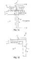
- FIGS. 1A and 1Bare a cross-sectional view and a lateral view illustrating a semiconductor structure that can be implemented within embodiments of the present invention.
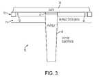
- FIG. 3is a cross-sectional view illustrating a semiconductor structure having a shared configuration between two semiconductor devices within the semiconductor structure that can be implemented within alternative embodiments of the present invention.
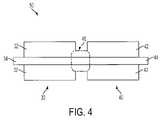
- FIG. 4is a top view illustrating the semiconductor structure as shown in FIG. 3 .
- FIG. 5is cross-sectional view illustrating a semiconductor structure that can be implemented within alternative embodiments of the present invention.
- FIG. 6is a top view of the semiconductor structure as shown in FIG. 5 .
- a multi-layer semiconductor structure 10e.g., a silicon-on-insulator (SOI) structure incorporating a deep trench capacitor 18 is provided in order to reduce SER of a semiconductor device within the semiconductor structure 10 .
- the multi-layer semiconductor structure 10includes a silicon-based substrate 12 such as a p-type substrate which acts as a handle wafer.
- An insulating layer 14(e.g., a thick buried oxide (BOX) layer) is formed on top of the p-type substrate 12 having a thickness of approximately 1000 Angstroms ( ⁇ ), via a low pressure chemical vapor deposition (LPCVD) process, for example.
- An active semiconductor layer 16 including n-type or p-type dopantsis then formed on top of the insulating layer 14 .
- a semiconductor device 22is formed within and on top of the active semiconductor layer 16 .
- the semiconductor device 22includes a gate 24 , source and drain regions 26 and a body/channel region 28 intermediate to the source and drain regions 26 and directly below the gate 24 .
- the deep trench capacitor 18(hereinafter referred to as “DT capacitor”) is formed by etching and drilling a trench through the active semiconductor layer 16 , the insulating layer 14 and in the p-type substrate 12 , prior to forming the semiconductor device 22 .
- the trenchis lined with an insulating material and a conductive material 20 is then deposited into the trench via a deposition process.
- the conductive material 20may be polysilicon or any suitable conductive material for the purposes disclosed herein may be used.
- the conductive material 20is doped polysilicon deposited via a low temperature epitaxial process.
- the conductive material 20is then recessed in the trench such that a top surface of the trench is within the insulating layer 14 .
- a dielectric collar material(not shown) is then deposited and a dielectric collar is formed by directional etching of the dielectric collar material leaving a dielectric spacer on the sidewall of the trench.
- a mask(not shown) is then used to remove the dielectric collar material where contact between the DT capacitor 18 and the body/channel region 28 is desired.
- the mask openingis smaller than the length of the gate 24 to prevent the trench material from shorting the channel to the source/drain regions 26 .
- Additional conductive material 20is deposited and planarized.
- the conductive material 20may be recessed into the trench such that the conductive material 20 remains in contact with the body/channel region 28 providing a desired electrical contact between the trench and the body/channel region 28 of the semiconductor device 22 , and a dielectric may be deposited and planarized in order to form an isolation region 41 (as depicted in FIG. 3 , for example) to electrically isolate the trench from all regions except the buried contact described above.
- the semiconductor device 22further includes contacts 27 which align the source and drain regions 26 .
- the DT capacitor 18is electrically connected with and contacts the body/channel region 28 , and is formed adjacent to the gate 24 , to add capacitance to the body/channel region 28 , which increases Qcrit and in turn reduces the SER of the semiconductor device 22 .
- the additional capacitancereduces the net voltage change of the body/channel region 28 , which enables the threshold voltage to remain stable and forces less current to be transmitted across the semiconductor device 22 .
- the semiconductor device 22is a NFET device that includes n+ source and drain regions 26 and a p+ body/channel region 28 beneath the gate 24 .
- the present inventionis not limited hereto, and any suitable device for the purpose described herein may be used.
- the DT capacitor 18is filled with the same type of silicon (p-type or n-type) as the body/channel region 28 of the device 22 to create an ohmic connection between the body/channel region 28 and the DT capacitor 18 .
- the body/channel region 28 and the DT capacitor 18are filled with p+ polysilicon.
- the DT capacitor 18is formed adjacent to an end portion of the body/channel region 28 beneath the gate 24 . Therefore, a conductive path extends from the body/channel region 28 to the end portion and to the DT capacitor 18 .
- FIG. 2illustrates a top view of the semiconductor structure 10 as taken along the line III-III as shown in FIG. 1 .
- FIG. 2illustrates the gate 24 , source and drain regions 26 and the DT capacitor 18 .
- a width of the DT capacitor 18is larger than a width of the gate 24 of the semiconductor device.
- the DT capacitor 18is formed such that it is adjacent to an end portion of the gate 24 and contacts with the body/channel region 28 (as depicted in FIGS. 1A and 1B ).
- the present inventionis not limited to the DT capacitor 18 being formed at a particular portion of the body/channel region 28 , and may vary as necessary. An alternative configuration will be described below with reference to FIGS. 5 and 6 .
- the DT capacitor 18is formed at an end portion of the body/channel region 28 as shown in FIGS. 1A and 2 , the DT capacitor may be shared between multiple semiconductor devices as described below with reference to FIGS. 3 and 4 , according to another embodiment of the present invention.
- FIGS. 3 and 4respectively illustrate a cross sectional view and a top view of a semiconductor structure that can be implemented within an alternative embodiment of the present invention.
- a semiconductor structure 50includes a plurality of semiconductor devices 30 and 40 .
- the semiconductor device 30includes the source and drain regions 32 , a body/channel region 33 and the gate 34
- the semiconductor device 40includes source and drain regions 42 , a body/channel region 43 and gate 44 .
- the semiconductor devices 30 and 40share a common gate formed on top of the active semiconductor layer 16 .
- the semiconductor structure 50includes a shared DT capacitor 46 shared between the semiconductor devices 30 and 40 , and is electrically connected to the body/channel regions 33 , 43 of both the semiconductor devices 30 and 40 .
- the shared DT capacitor 46is formed beneath adjacent end portions of the body/channel regions 33 , 43 of the plurality of semiconductor devices 30 and 40 , and contacts with the body/channel regions 33 , 43 and electrically connects the body/channel regions 33 , 43 to each other, thereby shunting them together.
- a width of the DT capacitor 46is larger than a width of each gate 34 and 44 of the semiconductor devices 30 and 40 .
- FIGS. 5 and 6illustrate a semiconductor structure that can be implemented according to alternative embodiments of the present invention.
- FIGS. 4 and 5illustrate an alternative configuration of the DT capacitor according to an embodiment of the present invention.
- a semiconductor structure 60according to an embodiment of the present invention, includes a PFET device 62 having p+ source and drain regions 64 , a gate 66 and an n+ body/channel region 68 formed directly below the gate 66 .
- a DT capacitor 70is formed below a center portion of the body/channel region 68 and electrically connects with and contacts the body/channel region 68 .
- the DT capacitor 70is filled with n+ polysilicon i.e., the same material as that of the body/channel region 68 , thereby creating a conductive path with the body/channel region 68 .
- the present inventiondiscloses a deep trench capacitor electrically connected with and contacting a body/channel region of a SOI device to increase the capacitance in the body/channel region, the higher capacitance reduces the voltage swing of the body/channel region during a charging event, and stabilizes the threshold voltage.
- the present inventionprovides a semiconductor structure that incorporates a deep trench capacitor for reducing the SER of a device within the semiconductor structure by increasing the Qcrit, thereby minimizing manufacturing costs.
Landscapes
- Engineering & Computer Science (AREA)
- Manufacturing & Machinery (AREA)
- Semiconductor Integrated Circuits (AREA)
- Thin Film Transistor (AREA)
Abstract
Description
Claims (16)
Priority Applications (2)
| Application Number | Priority Date | Filing Date | Title |
|---|---|---|---|
| US12/200,538US7989865B2 (en) | 2008-08-28 | 2008-08-28 | Deep trench capacitor for SOI CMOS devices for soft error immunity |
| US13/075,271US8133772B2 (en) | 2008-08-28 | 2011-03-30 | Deep trench capacitor for SOI CMOS devices for soft error immunity |
Applications Claiming Priority (1)
| Application Number | Priority Date | Filing Date | Title |
|---|---|---|---|
| US12/200,538US7989865B2 (en) | 2008-08-28 | 2008-08-28 | Deep trench capacitor for SOI CMOS devices for soft error immunity |
Related Child Applications (1)
| Application Number | Title | Priority Date | Filing Date |
|---|---|---|---|
| US13/075,271DivisionUS8133772B2 (en) | 2008-08-28 | 2011-03-30 | Deep trench capacitor for SOI CMOS devices for soft error immunity |
Publications (2)
| Publication Number | Publication Date |
|---|---|
| US20100052026A1 US20100052026A1 (en) | 2010-03-04 |
| US7989865B2true US7989865B2 (en) | 2011-08-02 |
Family
ID=41724008
Family Applications (2)
| Application Number | Title | Priority Date | Filing Date |
|---|---|---|---|
| US12/200,538ActiveUS7989865B2 (en) | 2008-08-28 | 2008-08-28 | Deep trench capacitor for SOI CMOS devices for soft error immunity |
| US13/075,271ActiveUS8133772B2 (en) | 2008-08-28 | 2011-03-30 | Deep trench capacitor for SOI CMOS devices for soft error immunity |
Family Applications After (1)
| Application Number | Title | Priority Date | Filing Date |
|---|---|---|---|
| US13/075,271ActiveUS8133772B2 (en) | 2008-08-28 | 2011-03-30 | Deep trench capacitor for SOI CMOS devices for soft error immunity |
Country Status (1)
| Country | Link |
|---|---|
| US (2) | US7989865B2 (en) |
Cited By (2)
| Publication number | Priority date | Publication date | Assignee | Title |
|---|---|---|---|---|
| US8586444B2 (en) | 2012-03-23 | 2013-11-19 | International Business Machines Corporation | Creating deep trenches on underlying substrate |
| US9059322B2 (en) | 2012-09-24 | 2015-06-16 | International Business Machines Corporation | Semiconductor-on-insulator (SOI) deep trench capacitor |
Families Citing this family (2)
| Publication number | Priority date | Publication date | Assignee | Title |
|---|---|---|---|---|
| US7977172B2 (en)* | 2008-12-08 | 2011-07-12 | Advanced Micro Devices, Inc. | Dynamic random access memory (DRAM) cells and methods for fabricating the same |
| US8513972B2 (en) | 2012-01-18 | 2013-08-20 | International Business Machines Corporation | Soft error resilient FPGA |
Citations (9)
| Publication number | Priority date | Publication date | Assignee | Title |
|---|---|---|---|---|
| US4873560A (en)* | 1987-04-01 | 1989-10-10 | Hitachi, Ltd. | Dynamic random access memory having buried word lines |
| US6399435B1 (en) | 1999-02-19 | 2002-06-04 | Infineon Technologies Ag | Method for producing a DRAM cell with a trench capacitor |
| US20030134468A1 (en) | 2001-06-04 | 2003-07-17 | Promos Technologies, Inc. | Aggressive capacitor array cell layout for narrow diameter DRAM trench capacitor structures via SOI technology |
| US20040000690A1 (en)* | 2001-10-24 | 2004-01-01 | Hiroshi Kujirai | Method of manufacturing semiconductor device and semiconductor device |
| US6696717B2 (en) | 2002-07-09 | 2004-02-24 | Nanya Technology Corporation | Memory cell with vertical transistor and trench capacitor |
| US7276753B2 (en) | 2004-09-25 | 2007-10-02 | Promos Technologies Inc. | Dynamic random access memory cell and fabricating method thereof |
| US7332392B2 (en) | 2006-04-11 | 2008-02-19 | United Microelectronics Corp. | Trench-capacitor DRAM device and manufacture method thereof |
| US7361933B2 (en) | 2004-03-31 | 2008-04-22 | Kabushiki Kaisha Toshiba | Semiconductor device |
| US20090026516A1 (en)* | 2007-07-24 | 2009-01-29 | Nanya Technology Corporation | Semiconductor memory device and fabrication method thereof |
- 2008
- 2008-08-28USUS12/200,538patent/US7989865B2/enactiveActive
- 2011
- 2011-03-30USUS13/075,271patent/US8133772B2/enactiveActive
Patent Citations (9)
| Publication number | Priority date | Publication date | Assignee | Title |
|---|---|---|---|---|
| US4873560A (en)* | 1987-04-01 | 1989-10-10 | Hitachi, Ltd. | Dynamic random access memory having buried word lines |
| US6399435B1 (en) | 1999-02-19 | 2002-06-04 | Infineon Technologies Ag | Method for producing a DRAM cell with a trench capacitor |
| US20030134468A1 (en) | 2001-06-04 | 2003-07-17 | Promos Technologies, Inc. | Aggressive capacitor array cell layout for narrow diameter DRAM trench capacitor structures via SOI technology |
| US20040000690A1 (en)* | 2001-10-24 | 2004-01-01 | Hiroshi Kujirai | Method of manufacturing semiconductor device and semiconductor device |
| US6696717B2 (en) | 2002-07-09 | 2004-02-24 | Nanya Technology Corporation | Memory cell with vertical transistor and trench capacitor |
| US7361933B2 (en) | 2004-03-31 | 2008-04-22 | Kabushiki Kaisha Toshiba | Semiconductor device |
| US7276753B2 (en) | 2004-09-25 | 2007-10-02 | Promos Technologies Inc. | Dynamic random access memory cell and fabricating method thereof |
| US7332392B2 (en) | 2006-04-11 | 2008-02-19 | United Microelectronics Corp. | Trench-capacitor DRAM device and manufacture method thereof |
| US20090026516A1 (en)* | 2007-07-24 | 2009-01-29 | Nanya Technology Corporation | Semiconductor memory device and fabrication method thereof |
Non-Patent Citations (1)
| Title |
|---|
| Wu, B. "Pillar Dram Cell With Dual Channels and an Underneath Trench-in-Trench Capacitor Built on Soi Structure", IBM Technical Disclosure Bulletin, Nov. 1993, pp. 141-144. |
Cited By (3)
| Publication number | Priority date | Publication date | Assignee | Title |
|---|---|---|---|---|
| US8586444B2 (en) | 2012-03-23 | 2013-11-19 | International Business Machines Corporation | Creating deep trenches on underlying substrate |
| US8860113B2 (en) | 2012-03-23 | 2014-10-14 | International Business Machines Corporation | Creating deep trenches on underlying substrate |
| US9059322B2 (en) | 2012-09-24 | 2015-06-16 | International Business Machines Corporation | Semiconductor-on-insulator (SOI) deep trench capacitor |
Also Published As
| Publication number | Publication date |
|---|---|
| US8133772B2 (en) | 2012-03-13 |
| US20100052026A1 (en) | 2010-03-04 |
| US20110177660A1 (en) | 2011-07-21 |
Similar Documents
| Publication | Publication Date | Title |
|---|---|---|
| US10546936B2 (en) | Structure for reduced source and drain contact to gate stack capacitance | |
| US10804203B2 (en) | Semiconductor device and fabrication method for the same | |
| US7952162B2 (en) | Semiconductor device and method for manufacturing the same | |
| US8048753B2 (en) | Charging protection device | |
| KR101050034B1 (en) | Floating body memory cell with gates advantageous for different conductivity type regions | |
| JP5172671B2 (en) | Method for manufacturing a dual gate CMOS structure, capacitor, and dual gate capacitor | |
| US7646039B2 (en) | SOI field effect transistor having asymmetric junction leakage | |
| KR100593739B1 (en) | Morse field effect transistor with body-source connection and its manufacturing method | |
| US7173302B2 (en) | Integrated circuit arrangement having capacitors and having planar transistors and fabrication method | |
| US8133772B2 (en) | Deep trench capacitor for SOI CMOS devices for soft error immunity | |
| US20140015051A1 (en) | Method of replacing silicon with metal in integrated circuit chip fabrication | |
| KR100609193B1 (en) | Semiconductor device and manufacturing method | |
| US20080012077A1 (en) | Semiconductor device | |
| JP2002111009A (en) | Substrate structure of SOI element and method of manufacturing the same | |
| US8053303B2 (en) | SOI body contact using E-DRAM technology | |
| US7638828B2 (en) | Embedded capacitor | |
| TW201513302A (en) | Asymmetric stress field effect transistor in dynamic unit | |
| KR101074232B1 (en) | Semiconductor device and manufacturing method thereof | |
| CN118629979A (en) | Semiconductor device and method for manufacturing the same | |
| KR20120042575A (en) | Method for manufacturing semiconductor device |
Legal Events
| Date | Code | Title | Description |
|---|---|---|---|
| AS | Assignment | Owner name:INTERNATIONAL BUSINESS MACHINES CORPORATION,NEW YO Free format text:ASSIGNMENT OF ASSIGNORS INTEREST;ASSIGNORS:BARTH, JOHN EDWARD, JR.;BERNSTEIN, KERRY;CANNON, ETHAN HARRISON;AND OTHERS;SIGNING DATES FROM 20080827 TO 20080828;REEL/FRAME:021458/0351 Owner name:INTERNATIONAL BUSINESS MACHINES CORPORATION, NEW Y Free format text:ASSIGNMENT OF ASSIGNORS INTEREST;ASSIGNORS:BARTH, JOHN EDWARD, JR.;BERNSTEIN, KERRY;CANNON, ETHAN HARRISON;AND OTHERS;SIGNING DATES FROM 20080827 TO 20080828;REEL/FRAME:021458/0351 | |
| STCF | Information on status: patent grant | Free format text:PATENTED CASE | |
| REMI | Maintenance fee reminder mailed | ||
| FPAY | Fee payment | Year of fee payment:4 | |
| SULP | Surcharge for late payment | ||
| AS | Assignment | Owner name:GLOBALFOUNDRIES U.S. 2 LLC, NEW YORK Free format text:ASSIGNMENT OF ASSIGNORS INTEREST;ASSIGNOR:INTERNATIONAL BUSINESS MACHINES CORPORATION;REEL/FRAME:036550/0001 Effective date:20150629 | |
| AS | Assignment | Owner name:GLOBALFOUNDRIES INC., CAYMAN ISLANDS Free format text:ASSIGNMENT OF ASSIGNORS INTEREST;ASSIGNORS:GLOBALFOUNDRIES U.S. 2 LLC;GLOBALFOUNDRIES U.S. INC.;REEL/FRAME:036779/0001 Effective date:20150910 | |
| AS | Assignment | Owner name:WILMINGTON TRUST, NATIONAL ASSOCIATION, DELAWARE Free format text:SECURITY AGREEMENT;ASSIGNOR:GLOBALFOUNDRIES INC.;REEL/FRAME:049490/0001 Effective date:20181127 | |
| MAFP | Maintenance fee payment | Free format text:PAYMENT OF MAINTENANCE FEE, 8TH YEAR, LARGE ENTITY (ORIGINAL EVENT CODE: M1552); ENTITY STATUS OF PATENT OWNER: LARGE ENTITY Year of fee payment:8 | |
| AS | Assignment | Owner name:GLOBALFOUNDRIES U.S. INC., CALIFORNIA Free format text:ASSIGNMENT OF ASSIGNORS INTEREST;ASSIGNOR:GLOBALFOUNDRIES INC.;REEL/FRAME:054633/0001 Effective date:20201022 | |
| AS | Assignment | Owner name:GLOBALFOUNDRIES INC., CAYMAN ISLANDS Free format text:RELEASE BY SECURED PARTY;ASSIGNOR:WILMINGTON TRUST, NATIONAL ASSOCIATION;REEL/FRAME:054636/0001 Effective date:20201117 | |
| AS | Assignment | Owner name:GLOBALFOUNDRIES U.S. INC., NEW YORK Free format text:RELEASE BY SECURED PARTY;ASSIGNOR:WILMINGTON TRUST, NATIONAL ASSOCIATION;REEL/FRAME:056987/0001 Effective date:20201117 | |
| MAFP | Maintenance fee payment | Free format text:PAYMENT OF MAINTENANCE FEE, 12TH YEAR, LARGE ENTITY (ORIGINAL EVENT CODE: M1553); ENTITY STATUS OF PATENT OWNER: LARGE ENTITY Year of fee payment:12 |