US7989824B2 - Method of forming a dielectric layer on a semiconductor light emitting device - Google Patents
Method of forming a dielectric layer on a semiconductor light emitting deviceDownload PDFInfo
- Publication number
- US7989824B2 US7989824B2US12/766,221US76622110AUS7989824B2US 7989824 B2US7989824 B2US 7989824B2US 76622110 AUS76622110 AUS 76622110AUS 7989824 B2US7989824 B2US 7989824B2
- Authority
- US
- United States
- Prior art keywords
- type region
- metal contact
- contact
- light emitting
- metal
- Prior art date
- Legal status (The legal status is an assumption and is not a legal conclusion. Google has not performed a legal analysis and makes no representation as to the accuracy of the status listed.)
- Active
Links
Images


Classifications
- H—ELECTRICITY
- H10—SEMICONDUCTOR DEVICES; ELECTRIC SOLID-STATE DEVICES NOT OTHERWISE PROVIDED FOR
- H10H—INORGANIC LIGHT-EMITTING SEMICONDUCTOR DEVICES HAVING POTENTIAL BARRIERS
- H10H20/00—Individual inorganic light-emitting semiconductor devices having potential barriers, e.g. light-emitting diodes [LED]
- H10H20/01—Manufacture or treatment
- H10H20/011—Manufacture or treatment of bodies, e.g. forming semiconductor layers
- H10H20/018—Bonding of wafers
- H—ELECTRICITY
- H10—SEMICONDUCTOR DEVICES; ELECTRIC SOLID-STATE DEVICES NOT OTHERWISE PROVIDED FOR
- H10H—INORGANIC LIGHT-EMITTING SEMICONDUCTOR DEVICES HAVING POTENTIAL BARRIERS
- H10H20/00—Individual inorganic light-emitting semiconductor devices having potential barriers, e.g. light-emitting diodes [LED]
- H10H20/80—Constructional details
- H10H20/81—Bodies
- H10H20/819—Bodies characterised by their shape, e.g. curved or truncated substrates
- H—ELECTRICITY
- H10—SEMICONDUCTOR DEVICES; ELECTRIC SOLID-STATE DEVICES NOT OTHERWISE PROVIDED FOR
- H10H—INORGANIC LIGHT-EMITTING SEMICONDUCTOR DEVICES HAVING POTENTIAL BARRIERS
- H10H20/00—Individual inorganic light-emitting semiconductor devices having potential barriers, e.g. light-emitting diodes [LED]
- H10H20/80—Constructional details
- H10H20/83—Electrodes
- H10H20/831—Electrodes characterised by their shape
- H—ELECTRICITY
- H10—SEMICONDUCTOR DEVICES; ELECTRIC SOLID-STATE DEVICES NOT OTHERWISE PROVIDED FOR
- H10H—INORGANIC LIGHT-EMITTING SEMICONDUCTOR DEVICES HAVING POTENTIAL BARRIERS
- H10H20/00—Individual inorganic light-emitting semiconductor devices having potential barriers, e.g. light-emitting diodes [LED]
- H10H20/80—Constructional details
- H10H20/84—Coatings, e.g. passivation layers or antireflective coatings
- H—ELECTRICITY
- H10—SEMICONDUCTOR DEVICES; ELECTRIC SOLID-STATE DEVICES NOT OTHERWISE PROVIDED FOR
- H10H—INORGANIC LIGHT-EMITTING SEMICONDUCTOR DEVICES HAVING POTENTIAL BARRIERS
- H10H20/00—Individual inorganic light-emitting semiconductor devices having potential barriers, e.g. light-emitting diodes [LED]
- H10H20/80—Constructional details
- H10H20/85—Packages
- H10H20/857—Interconnections, e.g. lead-frames, bond wires or solder balls
- H—ELECTRICITY
- H01—ELECTRIC ELEMENTS
- H01L—SEMICONDUCTOR DEVICES NOT COVERED BY CLASS H10
- H01L2924/00—Indexing scheme for arrangements or methods for connecting or disconnecting semiconductor or solid-state bodies as covered by H01L24/00
- H01L2924/0001—Technical content checked by a classifier
- H01L2924/0002—Not covered by any one of groups H01L24/00, H01L24/00 and H01L2224/00
Definitions
- This inventionrelates generally to semiconductor devices, and more specifically to using a dielectric layer to support a flip chip semiconductor light-emitting device and to electrically isolate the n- and p-contacts.
- LEDslight emitting diodes
- III-V semiconductorsparticularly binary, ternary, and quaternary alloys of gallium, aluminum, indium, and nitrogen, also referred to as III-nitride materials; and binary, ternary, and quaternary alloys of gallium, aluminum, indium, arsenic, and phosphorus.
- III-nitride devicesare epitaxially grown on sapphire, silicon carbide, or III-nitride substrates and III-phosphide devices are epitaxially grown on gallium arsenide by metal organic chemical vapor deposition (MOCVD), molecular beam epitaxy (MBE), or other epitaxial techniques.
- MOCVDmetal organic chemical vapor deposition
- MBEmolecular beam epitaxy
- an n-type regionis deposited on the substrate, then a light emitting or active region is deposited on the n-type region, then a p-type region is deposited on the active region. The order of the layers may be reversed such that the p-type region is adjacent to the substrate.
- FIG. 1illustrates a semiconductor device 30 described in more detail in US 2008/0081397, which is incorporated herein by reference.
- Device 30includes an epitaxial structure 32 .
- the epitaxial structure 32includes an n-type region 36 , which is grown on the substrate 34 .
- the epitaxial structure 32further includes a light emitting region 38 , grown on the n-type region 36 , and a p-type region 40 , which is grown on the light emitting region 38 .
- the n-type region 36 , the p-type region 40 , and the light emitting region 38may each include a plurality of layers of different composition and dopant concentration.
- the n-type region 36may include a release layer (not shown) located between the n-type region and the substrate, for facilitating release of the substrate from the epitaxial structure 32 .
- a p-metal layer 44which generally comprises a highly reflective metal, is formed in electrical contact with the p-type region 40 .
- An optional guard layer 46may be deposited over the p-metal layer 44 .
- the guard layer 46may be used, for example, when the p-metal layer 44 comprises silver, in which case the guard layer is included to prevent silver from migrating to other parts of the epitaxial structure 32 .
- the guard layer 46is in electrical contact with the p-metal layer 44 .
- One or more p-electrode metal layers 48may be deposited over the guard layer 46 and in electrical connection therewith. In the case of a dielectric guard layer, a via hole may be etched through the guard layer to facilitate contact between p-electrode metal layers 48 and p-metal layer 44 .
- the epitaxial structure 32further includes one or more voids 50 .
- the voids 50facilitate electrical connection to the n-type region 36 .
- a dielectric layer 52is deposited over the guard metal layers 46 and side wall surfaces of the voids 50 .
- the epitaxial structure 32also includes an n-electrode metal layer 56 deposited over the dielectric layer 52 and the bottom surface of void 50 .
- the n-electrode layer 56 at the bottom of the void 50is in electrical connection with the n-type region 36 , and provides an electrical connection thereto.
- the dielectric layer 52electrically insulates the n-electrodes 56 from the p-electrode 48 , the guard metal layer 46 , and the p-type region 40 .
- the voids 50may further include a trench which is operable to electrically insulate the p-electrode 48 from the n-electrodes 56 .
- the voids 50weaken the semiconductor structure 30 , making the structure susceptible to damage during mounting and/or operation.
- a support material 110substantially fills the voids 50 .
- the support material 110is sufficiently solidified to support the semiconductor structure 30 during mounting and/or operation.
- the support material 110has a glass transition temperature greater than the operating temperature of the semiconductor light emitting structure 30 , such that the support material remains sufficiently rigid to support the semiconductor structure when operating to generate light.
- the support material 110overfills the voids 50 and covers at least a portion of an upper surface 112 of the epitaxial structure 32 .
- the support material 110may be deposited by spin coating a wafer (not shown) including a plurality of semiconductor structures 30 .
- Spin coatinginvolves depositing more than a sufficient quantity of a fluid support material 110 , and then spinning the wafer to cause the fluid to form a thin coating over the wafer. Spinning continues until the coating has sufficiently cured through evaporation of solvents, for example.
- the support material 110may then be further cured by baking the wafer in an oven to raise the temperature above the support material cure temperature to solidify the support material sufficiently to support the semiconductor structure 30 .
- Planarizingmay involve mechanical process steps such as lapping the wafer to abrade away excess support material 110 .
- lappingmay remove a portion of the n-electrode layer 56 and the p-electrode 48 , to provide a substantially flat mounting surface.
- Mechanical lappingmay also be combined with chemical etching.
- a semiconductor structurecomprising a light emitting layer disposed between an n-type region and a p-type region is formed.
- a first metal contactis formed on a portion of the n-type region and a second metal contact is formed on a portion of the p-type region.
- the first and second metal contactsare formed on a same side of the semiconductor structure.
- a dielectric materialis disposed between the first and second metal contacts. The dielectric material is in direct contact with a portion of the semiconductor structure, a portion of the first metal contact, and a portion of the second metal contact.
- a planar surfaceis formed including a surface of the first metal contact, a surface of the second metal contact, and a surface of the dielectric material.
- FIG. 1illustrates a III-nitride light emitting device with a support material filling voids in the device.
- FIG. 2illustrates the device of FIG. 1 after planarizing the support material to expose the n- and p-electrodes.
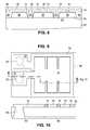
- FIG. 3is a plan view of a light emitting device according to embodiments of the invention.
- FIGS. 4 and 5are cross sectional views of the device illustrated in FIG. 3 .
- FIG. 6is a plan view of a mount on which the device illustrated in FIG. 3 may be mounted.
- FIG. 7is a cross sectional view of the mount illustrated in FIG. 6 .
- FIG. 8is a cross sectional view of a light emitting device with redistributed electrical contacts, according to embodiments of the invention.
- FIG. 9is a plan view of an alternative mount on which the device illustrated in FIG. 3 may be mounted.
- FIG. 10is a cross sectional view of the mount illustrated in FIG. 9 .
- the device illustrated in FIGS. 1 and 2requires a buried intermetal dielectric layer 52 .
- Particles or voids present before or generated during the deposition of buried dielectric layer 52may cause device shorts.
- the use of such a dielectric layer 52requires strict contamination control and wafer cleanliness in order to achieve high manufacturing yields.
- the dielectric material deposited to support the diealso serves to electrically isolate the n- and p-metal contacts, eliminating the need for a buried dielectric layer 52 as illustrated in FIGS. 1 and 2 .
- FIG. 3is a plan view of an LED according to embodiments of the device.
- FIGS. 4 and 5are cross sectional views along the axes shown in FIG. 3 .
- the LEDincludes a semiconductor structure, including one or more light emitting layers sandwiched between an n-type region and a p-type region.
- the semiconductor structureis a III-nitride structure, and the light emitting layers are configured to emit blue light, though any suitable semiconductor structure, such as any group III-V structure including III-P and III-As structures, may be used.
- a III-nitride structureis typically grown on a sapphire or SiC growth substrate 60 by growing the n-type region, followed by the light emitting region, followed by the p-type region. The growth substrate may be removed from the semiconductor structure after growth.
- the n-type region 62may include multiple layers of different compositions and dopant concentration including, for example, preparation layers such as buffer layers or nucleation layers which may be n-type or not intentionally doped, release layers designed to facilitate later release of the growth substrate or thinning of the semiconductor structure after substrate removal, and n- or even p-type device layers designed for particular optical or electrical properties desirable for the light emitting region to efficiently emit light.
- preparation layerssuch as buffer layers or nucleation layers which may be n-type or not intentionally doped
- release layersdesigned to facilitate later release of the growth substrate or thinning of the semiconductor structure after substrate removal
- n- or even p-type device layersdesigned for particular optical or electrical properties desirable for the light emitting region to efficiently emit light.
- the light emitting region 64is grown over the n-type region 62 .
- suitable light emitting regionsinclude a single thick or thin light emitting layer and a multiple quantum well light emitting region including multiple thin or thick quantum well light emitting layers separated by barrier layers.
- a multiple quantum well light emitting regionmay include multiple InGaN light emitting layers separated by GaN or InGaN barriers.
- One or more light emitting layers in the devicemay be doped, for example with Si, or the light emitting layer or layers may be not intentionally doped.
- the p-type region 66is grown over the light emitting region 64 .
- the p-type regionmay include multiple layers of different composition, thickness, and dopant concentration, including layers that are not intentionally doped, or n-type layers.
- N-contact 68is formed on the exposed portion of n-type region 62 and p-contact 70 is formed on the remaining portion of p-type region 66 .
- the n-contact 68surrounds the device and includes several fingers which extend toward the center of the device.
- the shortest distance between two points on the n-contactis not more than twice the current spreading distance in n-type region 62 .
- n-contact 68is thicker than p-contact 70 , such that the tops of the n- and p-contacts are at roughly the same height, or such that the top of the n-contact is taller than the top of the p-contact.
- a dielectric material 74electrically isolates the n- and p-contacts 68 and 70 .
- Dielectric material 74may be, for example, a polymer such as polyimide or benzocyclobutene-based (BCB), or an inorganic material such as silicon dioxide or silicon nitride.
- Dielectric material 74may be deposited in such a way that it fills any voids in the device.
- the LED illustrated in FIGS. 3-5is formed by growing the semiconductor structure on the growth substrate, then patterning the semiconductor structure to expose a portion of the n-type region on which the n-contact is formed. In some embodiments, one or more metal layers are then deposited and patterned to form the n- and p-contacts. A thick layer of dielectric material is deposited on the surface to encapsulate the n- and p-contacts and fill any voids between them.
- the dielectric material 74may be, for example, spun-on polyimide or silicon nitride formed by plasma-enhanced chemical vapor deposition, chemical vapor deposition, or a suitable vacuum deposition technique.
- the top surface of the deviceis then planarized, for example by chemical mechanical polishing (CMP), to remove any dielectric material covering the n- and p-contacts, and to form a planar surface.
- CMPchemical mechanical polishing
- the dielectric material remaining between the n- and p-contactsis etched to slightly below the top surface of the n- and p-contacts, to prevent the dielectric material from interfering with bonding the n- and p-contacts to a mount.
- the etched thicknessmay be in the order of 100 nm to 500 nm and can be done by wet chemical or plasma etching.
- a thick dielectric layeris deposited first. Openings for the n- and p-contacts are patterned into the dielectric, then the n- and p-contacts are formed in the openings, for example by electroplating, evaporation, or any other suitable technique. If BCB is used as the dielectric, openings can be formed lithographically before curing. The top surface of the device is then planarized, for example by CMP, to remove any excess contact metal and to expose the top surface of the dielectric material between the contacts. The dielectric material may then be etched as described above.
- the deposition and annealing of metal contact layersmay also occur before the patterning of the semiconductor structure in case of the p-contact, or before the deposition of dielectric material 74 in the case of both n- and/or p-contacts.
- the openings in the dielectric materialreveal the underlying thin contact layers.
- the openingsare filled with metal and subsequently planarized, as described above.
- a compliant bonding structureis formed on one or both of the p-contact and n-contact planarized surfaces.
- the compliant bonding structuremay be, for example, a group of metal bumps with 1:2 or higher aspect ratios to facilitate bonding of large area metal surfaces.
- the bumpsmay have diameters and heights between 1 and 10 microns. Bumps less than 3 microns tall may be formed by, for example, evaporation and lift-off techniques; taller bumps may be formed by, for example, electroplating.
- the compliant bonding structurecollapses in a solid phase, unlike solder which liquefies during bonding.
- the compliant bonding structureelectrically and mechanically connects the semiconductor structure to the mount.
- Compliant bonding structuresare described in more detail in “Method of Bonding a Semiconductor Device Using a Compliant Bonding Structure,” U.S. application Ser. No. 12/397,367, which is incorporated herein by reference.
- FIG. 6is a plan view of a structure on which the device illustrated in FIGS. 3-5 may be mounted.
- FIG. 7is a cross sectional view of the mount along the axis indicated in FIG. 6 .
- the mountincludes p-contact 78 and n-contact 76 , which mirror the p- and n-contacts 70 and 68 on the LED.
- the p- and n-contacts on the mountare electrically isolated by insulating material 80 .
- N- and p-contact pads 82 and 84are formed on the mount for electrically connecting the LED to another structure such as, for example, a power source.
- a portion of the n-contact surrounding the p-type regionis removed or omitted.
- the spaceis filled with a thick dielectric layer.
- the dielectric materialforms a contact “bridge” 72 which allows a trace to p-contact pad 84 on the mount to electrically connect to the LED's p-contact 70 , which is otherwise surrounded by the n-contact 68 , without shorting the n-contact 68 .
- FIG. 9is a plan view of an alternative mount on which the device illustrated in FIGS. 3-5 may be mounted.
- FIG. 10is a cross sectional view of the mount along the axis indicated in FIG. 9 .
- the mountincludes p-contact 78 and n-contact 76 , which mirror the p- and n-contacts 70 and 68 on the LED.
- the p- and n-contacts on the mountare electrically isolated by insulating material 80 .
- N- and p-contact pads 82 and 84are formed on the mount for electrically connecting the LED to another structure such as, for example, a power source.
- One or more vias 86may be formed through insulating material 80 , to connect the n- and p-contact pads 82 and 84 to contact pads 87 and 88 formed on the bottom of the mount.
- the via shown in FIG. 10connects p-contact pad 84 to a p-contact pad 87 on the bottom of the mount.
- the LEDmay be connected to the mount by, for example, solder, a thermocompression bond, an interdiffusion bond, or a Au stud bump array bonded by an ultrasonic weld.
- Growth substrate 60may be removed after mounting the LED on the mount, by a process appropriate to the growth substrate such as, for example, laser melting or etching.
- the semiconductor structuremay be thinned after removing the growth substrate, for example by photoelectrochemical etching, and/or textured or patterned, for example with a rough surface or a photonic crystal.
- a wavelength converting materialsuch as one or more phosphors, and/or other known structures such as a dichroic filter, a polarizer, or a lens or other optical device may be disposed over the semiconductor structure.
- the dielectric materialis used to redistribute the n- and p-contacts, as illustrated in FIG. 8 .
- the semiconductor structureis grown, then patterned to expose portions of the n-type region 62 , then the n- and p-contacts 68 and 70 are formed, then a thick dielectric material 74 is disposed over the structure, as described above in reference to FIGS. 3-5 .
- the dielectric material 74may be optionally planarized, without exposing the top surfaces of n- and p-contacts 68 and 70 .
- openings 90 in the dielectric material 74are formed which align with the n-contacts 68 .
- openings 91 in the dielectric material 75are formed which align with the p-contacts 70 .
- the openingsare then filled with a conductive material, typically metal.
- a large area n-contact 92is formed on the left side of the device and a large area p-contact 93 is formed on the right side of the device.
- An insulating material 95is then deposited over and electrically isolates the large area n- and p-contacts 92 and 93 .
- the structureis then planarized, exposing the contacts 92 and 93 .
- a device with large area contacts as illustrated in FIG. 8may simply the design of the mount.
- Embodiments of the inventionmay have several advantages.
- the dielectric materialis formed by a process that fills all the voids in the device, thus the semiconductor structure is fully supported during and after removal of the substrate, which may reduce the frequency of cracking of the semiconductor during removal of the substrate.
- the device structureneed not include any additional underfill material.
- the intermetal dielectric described above in reference to FIGS. 1 and 2which is susceptible to cracking and defects caused by particles and/or voids, is eliminated, which may improve the thermal performance of the device and the yield, by eliminating problems caused by flaws in the intermetal dielectric.
- the deviceis planarized in wafer form, which may eliminate problems associated with non-planarity during flip chip bonding. Also, thick, expensive, plated metal contacts are not required to overcome any non-planarities that may interfere with bonding to the mount.
Landscapes
- Led Devices (AREA)
- Internal Circuitry In Semiconductor Integrated Circuit Devices (AREA)
- Electrodes Of Semiconductors (AREA)
Abstract
Description
Claims (6)
Priority Applications (7)
| Application Number | Priority Date | Filing Date | Title |
|---|---|---|---|
| US12/766,221US7989824B2 (en) | 2009-06-03 | 2010-04-23 | Method of forming a dielectric layer on a semiconductor light emitting device |
| CN201080024817.2ACN102460737B (en) | 2009-06-03 | 2010-05-27 | Method of forming a dielectric layer on a semiconductor light emitting device |
| PCT/IB2010/052372WO2010140091A2 (en) | 2009-06-03 | 2010-05-27 | Method of forming a dielectric layer on a semiconductor light emitting device |
| KR1020167036008AKR101811673B1 (en) | 2009-06-03 | 2010-05-27 | Method of forming a dielectric layer on a semiconductor light emitting device |
| JP2012513705AJP5771198B2 (en) | 2009-06-03 | 2010-05-27 | Method for forming a dielectric layer on a semiconductor light emitting device |
| EP10726299.0AEP2438625B8 (en) | 2009-06-03 | 2010-05-27 | Method of forming a dielectric layer on a semiconductor light emitting device, and semiconductor light emitting device with a dielectric layer |
| KR1020127000136AKR101690705B1 (en) | 2009-06-03 | 2010-05-27 | Method of forming a dielectric layer on a semiconductor light emitting device |
Applications Claiming Priority (2)
| Application Number | Priority Date | Filing Date | Title |
|---|---|---|---|
| US12/477,222US7732231B1 (en) | 2009-06-03 | 2009-06-03 | Method of forming a dielectric layer on a semiconductor light emitting device |
| US12/766,221US7989824B2 (en) | 2009-06-03 | 2010-04-23 | Method of forming a dielectric layer on a semiconductor light emitting device |
Related Parent Applications (1)
| Application Number | Title | Priority Date | Filing Date |
|---|---|---|---|
| US12/477,222DivisionUS7732231B1 (en) | 2009-06-03 | 2009-06-03 | Method of forming a dielectric layer on a semiconductor light emitting device |
Publications (2)
| Publication Number | Publication Date |
|---|---|
| US20100308367A1 US20100308367A1 (en) | 2010-12-09 |
| US7989824B2true US7989824B2 (en) | 2011-08-02 |
Family
ID=42671701
Family Applications (1)
| Application Number | Title | Priority Date | Filing Date |
|---|---|---|---|
| US12/766,221ActiveUS7989824B2 (en) | 2009-06-03 | 2010-04-23 | Method of forming a dielectric layer on a semiconductor light emitting device |
Country Status (6)
| Country | Link |
|---|---|
| US (1) | US7989824B2 (en) |
| EP (1) | EP2438625B8 (en) |
| JP (1) | JP5771198B2 (en) |
| KR (2) | KR101811673B1 (en) |
| CN (1) | CN102460737B (en) |
| WO (1) | WO2010140091A2 (en) |
Families Citing this family (11)
| Publication number | Priority date | Publication date | Assignee | Title |
|---|---|---|---|---|
| US8471282B2 (en) | 2010-06-07 | 2013-06-25 | Koninklijke Philips Electronics N.V. | Passivation for a semiconductor light emitting device |
| US9070851B2 (en)* | 2010-09-24 | 2015-06-30 | Seoul Semiconductor Co., Ltd. | Wafer-level light emitting diode package and method of fabricating the same |
| KR20120082715A (en)* | 2011-01-14 | 2012-07-24 | 삼성엘이디 주식회사 | Semiconductor light emitting device and manufacturing method thereof |
| WO2013084155A1 (en)* | 2011-12-08 | 2013-06-13 | Koninklijke Philips Electronics N.V. | Forming thick metal layers on a semiconductor light emitting device |
| US9704774B2 (en) | 2012-12-11 | 2017-07-11 | Sensor Electronic Technology, Inc. | Thermal management structure with integrated heat sink |
| US9577172B2 (en) | 2013-02-19 | 2017-02-21 | Koninklijke Philips N.V. | Light emitting die component formed by multilayer structures |
| EP3017483B1 (en)* | 2013-07-03 | 2020-05-06 | Lumileds Holding B.V. | Led with stress-buffer layer under metallization layer |
| KR101493354B1 (en)* | 2013-09-25 | 2015-02-16 | 한국광기술원 | Light emitting diode device and method for manufacturing the same |
| WO2016021919A1 (en)* | 2014-08-05 | 2016-02-11 | 서울바이오시스 주식회사 | Light-emitting diode and manufacturing method therefor |
| JP5985782B1 (en)* | 2015-04-03 | 2016-09-06 | 創光科学株式会社 | Nitride semiconductor ultraviolet light emitting device and nitride semiconductor ultraviolet light emitting device |
| CN112792735B (en)* | 2021-01-20 | 2022-04-05 | 北京科技大学 | Clamp for inhibiting generation and expansion of grinding and polishing cracks of diamond film and using method |
Citations (8)
| Publication number | Priority date | Publication date | Assignee | Title |
|---|---|---|---|---|
| US6891197B2 (en) | 2001-05-09 | 2005-05-10 | Lumileds Lighting U.S., Llc | Semiconductor LED flip-chip with dielectric coating on the mesa |
| US20060240585A1 (en) | 2004-10-28 | 2006-10-26 | Philips Lumileds Lighting Company, Llc | Package-Integrated Thin Film LED |
| US20070096130A1 (en) | 2005-06-09 | 2007-05-03 | Philips Lumileds Lighting Company, Llc | LED Assembly Having Maximum Metal Support for Laser Lift-Off of Growth Substrate |
| US7220608B2 (en)* | 2001-12-03 | 2007-05-22 | Sony Corporation | Transferring semiconductor crystal from a substrate to a resin |
| US20080081397A1 (en) | 2006-09-28 | 2008-04-03 | Philips Lumileds Lighting Company, Llc | Process for Preparing a Semiconductor Structure for Mounting |
| US20080173884A1 (en) | 2007-01-22 | 2008-07-24 | Cree, Inc. | Wafer level phosphor coating method and devices fabricated utilizing method |
| DE102007003282A1 (en) | 2007-01-23 | 2008-07-24 | Osram Opto Semiconductors Gmbh | LED chip |
| WO2009020365A2 (en) | 2007-08-08 | 2009-02-12 | Korea Photonics Technology Institute | Light emitting diode with metal piles and multi-passivation layers and its manufacturing method |
Family Cites Families (21)
| Publication number | Priority date | Publication date | Assignee | Title |
|---|---|---|---|---|
| JPH08298344A (en)* | 1995-04-27 | 1996-11-12 | Hitachi Ltd | Light emitting diode device and manufacturing method thereof |
| JP2000299405A (en)* | 1999-04-15 | 2000-10-24 | Rohm Co Ltd | Manufacture of semiconductor device |
| JP4667556B2 (en)* | 2000-02-18 | 2011-04-13 | 古河電気工業株式会社 | Vertical GaN-based field effect transistor, bipolar transistor and vertical GaN-based field effect transistor manufacturing method |
| US6288426B1 (en)* | 2000-02-28 | 2001-09-11 | International Business Machines Corp. | Thermal conductivity enhanced semiconductor structures and fabrication processes |
| JP4465891B2 (en)* | 2001-02-07 | 2010-05-26 | パナソニック株式会社 | Semiconductor device |
| JP4081985B2 (en)* | 2001-03-02 | 2008-04-30 | 日亜化学工業株式会社 | Light emitting device and manufacturing method thereof |
| JP4529319B2 (en)* | 2001-06-27 | 2010-08-25 | 日亜化学工業株式会社 | Semiconductor chip and manufacturing method thereof |
| CN1732714B (en)* | 2002-12-26 | 2011-07-13 | 株式会社半导体能源研究所 | Light emitting device |
| JP2005079551A (en)* | 2003-09-03 | 2005-03-24 | Toyoda Gosei Co Ltd | A composite substrate for forming a semiconductor light emitting device, a method for manufacturing the same, and a method for manufacturing a semiconductor light emitting device. |
| JP2005086137A (en)* | 2003-09-11 | 2005-03-31 | Mitsubishi Cable Ind Ltd | GaN-based light emitting diode |
| JP4258338B2 (en)* | 2003-10-09 | 2009-04-30 | 日立電線株式会社 | LIGHT EMITTING DEVICE, WIRING BOARD USED FOR LIGHT EMITTING DEVICE, AND WIRING BOARD MANUFACTURING METHOD |
| JP2005347647A (en)* | 2004-06-04 | 2005-12-15 | Sony Corp | Element and element transfer method |
| US20060131708A1 (en)* | 2004-12-16 | 2006-06-22 | Ng Kee Y | Packaged electronic devices, and method for making same |
| US7348212B2 (en)* | 2005-09-13 | 2008-03-25 | Philips Lumileds Lighting Company Llc | Interconnects for semiconductor light emitting devices |
| JP4462249B2 (en)* | 2005-09-22 | 2010-05-12 | ソニー株式会社 | Light emitting diode manufacturing method, integrated light emitting diode manufacturing method, and nitride III-V compound semiconductor growth method |
| CN101317253B (en)* | 2005-11-28 | 2010-10-27 | Nxp股份有限公司 | Method for fabricating self-aligned Schottky junctions for semiconductor devices |
| JP2007184411A (en) | 2006-01-06 | 2007-07-19 | Sony Corp | LIGHT EMITTING DIODE AND ITS MANUFACTURING METHOD, INTEGRATED LIGHT EMITTING DIODE AND ITS MANUFACTURING METHOD, LIGHT EMITTING DIODE BACKLIGHT AND LIGHT EMITTING DIODE LIGHTING DEVICE |
| JP2007335734A (en)* | 2006-06-16 | 2007-12-27 | Renesas Technology Corp | Semiconductor device |
| JP2008047834A (en)* | 2006-08-21 | 2008-02-28 | Hamamatsu Photonics Kk | Semiconductor device and manufacturing method of semiconductor device |
| TWM315146U (en) | 2007-01-19 | 2007-07-11 | Kantas Products Co Ltd | Single-handled spring-assisted folding knives |
| JP2008160158A (en)* | 2008-03-21 | 2008-07-10 | Fujitsu Ltd | Semiconductor device |
- 2010
- 2010-04-23USUS12/766,221patent/US7989824B2/enactiveActive
- 2010-05-27WOPCT/IB2010/052372patent/WO2010140091A2/enactiveApplication Filing
- 2010-05-27CNCN201080024817.2Apatent/CN102460737B/enactiveActive
- 2010-05-27KRKR1020167036008Apatent/KR101811673B1/enactiveActive
- 2010-05-27JPJP2012513705Apatent/JP5771198B2/enactiveActive
- 2010-05-27KRKR1020127000136Apatent/KR101690705B1/enactiveActive
- 2010-05-27EPEP10726299.0Apatent/EP2438625B8/enactiveActive
Patent Citations (8)
| Publication number | Priority date | Publication date | Assignee | Title |
|---|---|---|---|---|
| US6891197B2 (en) | 2001-05-09 | 2005-05-10 | Lumileds Lighting U.S., Llc | Semiconductor LED flip-chip with dielectric coating on the mesa |
| US7220608B2 (en)* | 2001-12-03 | 2007-05-22 | Sony Corporation | Transferring semiconductor crystal from a substrate to a resin |
| US20060240585A1 (en) | 2004-10-28 | 2006-10-26 | Philips Lumileds Lighting Company, Llc | Package-Integrated Thin Film LED |
| US20070096130A1 (en) | 2005-06-09 | 2007-05-03 | Philips Lumileds Lighting Company, Llc | LED Assembly Having Maximum Metal Support for Laser Lift-Off of Growth Substrate |
| US20080081397A1 (en) | 2006-09-28 | 2008-04-03 | Philips Lumileds Lighting Company, Llc | Process for Preparing a Semiconductor Structure for Mounting |
| US20080173884A1 (en) | 2007-01-22 | 2008-07-24 | Cree, Inc. | Wafer level phosphor coating method and devices fabricated utilizing method |
| DE102007003282A1 (en) | 2007-01-23 | 2008-07-24 | Osram Opto Semiconductors Gmbh | LED chip |
| WO2009020365A2 (en) | 2007-08-08 | 2009-02-12 | Korea Photonics Technology Institute | Light emitting diode with metal piles and multi-passivation layers and its manufacturing method |
Also Published As
| Publication number | Publication date |
|---|---|
| CN102460737A (en) | 2012-05-16 |
| KR101690705B1 (en) | 2016-12-29 |
| CN102460737B (en) | 2015-04-08 |
| JP5771198B2 (en) | 2015-08-26 |
| WO2010140091A2 (en) | 2010-12-09 |
| KR101811673B1 (en) | 2017-12-22 |
| KR20170010405A (en) | 2017-01-31 |
| JP2012529172A (en) | 2012-11-15 |
| KR20120027458A (en) | 2012-03-21 |
| US20100308367A1 (en) | 2010-12-09 |
| EP2438625B1 (en) | 2018-07-11 |
| EP2438625A2 (en) | 2012-04-11 |
| WO2010140091A3 (en) | 2011-02-17 |
| EP2438625B8 (en) | 2018-08-29 |
Similar Documents
| Publication | Publication Date | Title |
|---|---|---|
| US7989824B2 (en) | Method of forming a dielectric layer on a semiconductor light emitting device | |
| US12199082B2 (en) | Method of direct-bonded optoelectronic devices | |
| US7732231B1 (en) | Method of forming a dielectric layer on a semiconductor light emitting device | |
| US8236584B1 (en) | Method of forming a light emitting diode emitter substrate with highly reflective metal bonding | |
| US9705047B2 (en) | Method of attaching a light emitting device to a support substrate | |
| JP2019114804A (en) | Light-emitting device bonded to supporting substrate | |
| US8053905B2 (en) | Compliant bonding structures for semiconductor devices | |
| KR102129146B1 (en) | Sealed semiconductor light emitting device | |
| TWI573300B (en) | Semiconductor light emitting device and method of manufacturing same | |
| US20240097087A1 (en) | Method of Transferring Patterned Micro-LED Die onto a Silicon Carrier for Wafer-to-Wafer Hybrid Bonding to a CMOS Backplane | |
| WO2013050898A1 (en) | Electrically insulating bond for mounting a light emitting device | |
| WO2013057668A1 (en) | Led wafer bonded to carrier wafer for wafer level processing |
Legal Events
| Date | Code | Title | Description |
|---|---|---|---|
| STCF | Information on status: patent grant | Free format text:PATENTED CASE | |
| FPAY | Fee payment | Year of fee payment:4 | |
| AS | Assignment | Owner name:DEUTSCHE BANK AG NEW YORK BRANCH, AS COLLATERAL AGENT, NEW YORK Free format text:SECURITY INTEREST;ASSIGNOR:LUMILEDS LLC;REEL/FRAME:043108/0001 Effective date:20170630 Owner name:DEUTSCHE BANK AG NEW YORK BRANCH, AS COLLATERAL AG Free format text:SECURITY INTEREST;ASSIGNOR:LUMILEDS LLC;REEL/FRAME:043108/0001 Effective date:20170630 | |
| AS | Assignment | Owner name:KONINKLIJKE PHILIPS N.V., NETHERLANDS Free format text:CHANGE OF NAME;ASSIGNOR:KONINKLIJKE PHILIPS ELECTRONICS N V;REEL/FRAME:046772/0611 Effective date:20170428 | |
| AS | Assignment | Owner name:LUMILEDS LLC, CALIFORNIA Free format text:ASSIGNMENT OF ASSIGNORS INTEREST;ASSIGNOR:KONINKLIJKE PHILIPS N.V.;REEL/FRAME:048150/0603 Effective date:20170428 | |
| MAFP | Maintenance fee payment | Free format text:PAYMENT OF MAINTENANCE FEE, 8TH YEAR, LARGE ENTITY (ORIGINAL EVENT CODE: M1552); ENTITY STATUS OF PATENT OWNER: LARGE ENTITY Year of fee payment:8 | |
| AS | Assignment | Owner name:SOUND POINT AGENCY LLC, NEW YORK Free format text:SECURITY INTEREST;ASSIGNORS:LUMILEDS LLC;LUMILEDS HOLDING B.V.;REEL/FRAME:062299/0338 Effective date:20221230 | |
| MAFP | Maintenance fee payment | Free format text:PAYMENT OF MAINTENANCE FEE, 12TH YEAR, LARGE ENTITY (ORIGINAL EVENT CODE: M1553); ENTITY STATUS OF PATENT OWNER: LARGE ENTITY Year of fee payment:12 | |
| AS | Assignment | Owner name:LUMILEDS HOLDING B.V., NETHERLANDS Free format text:RELEASE BY SECURED PARTY;ASSIGNOR:SOUND POINT AGENCY LLC;REEL/FRAME:070046/0001 Effective date:20240731 Owner name:LUMILEDS LLC, CALIFORNIA Free format text:RELEASE BY SECURED PARTY;ASSIGNOR:SOUND POINT AGENCY LLC;REEL/FRAME:070046/0001 Effective date:20240731 |