US7989362B2 - Hafnium lanthanide oxynitride films - Google Patents
Hafnium lanthanide oxynitride filmsDownload PDFInfo
- Publication number
- US7989362B2 US7989362B2US12/505,963US50596309AUS7989362B2US 7989362 B2US7989362 B2US 7989362B2US 50596309 AUS50596309 AUS 50596309AUS 7989362 B2US7989362 B2US 7989362B2
- Authority
- US
- United States
- Prior art keywords
- dielectric
- forming
- hflnon
- layer
- precursor
- Prior art date
- Legal status (The legal status is an assumption and is not a legal conclusion. Google has not performed a legal analysis and makes no representation as to the accuracy of the status listed.)
- Active
Links
Images


Classifications
- H—ELECTRICITY
- H01—ELECTRIC ELEMENTS
- H01L—SEMICONDUCTOR DEVICES NOT COVERED BY CLASS H10
- H01L21/00—Processes or apparatus adapted for the manufacture or treatment of semiconductor or solid state devices or of parts thereof
- H01L21/02—Manufacture or treatment of semiconductor devices or of parts thereof
- H01L21/02104—Forming layers
- H01L21/02107—Forming insulating materials on a substrate
- H01L21/02109—Forming insulating materials on a substrate characterised by the type of layer, e.g. type of material, porous/non-porous, pre-cursors, mixtures or laminates
- H01L21/02112—Forming insulating materials on a substrate characterised by the type of layer, e.g. type of material, porous/non-porous, pre-cursors, mixtures or laminates characterised by the material of the layer
- H01L21/02172—Forming insulating materials on a substrate characterised by the type of layer, e.g. type of material, porous/non-porous, pre-cursors, mixtures or laminates characterised by the material of the layer the material containing at least one metal element, e.g. metal oxides, metal nitrides, metal oxynitrides or metal carbides
- H01L21/02175—Forming insulating materials on a substrate characterised by the type of layer, e.g. type of material, porous/non-porous, pre-cursors, mixtures or laminates characterised by the material of the layer the material containing at least one metal element, e.g. metal oxides, metal nitrides, metal oxynitrides or metal carbides characterised by the metal
- H01L21/02194—Forming insulating materials on a substrate characterised by the type of layer, e.g. type of material, porous/non-porous, pre-cursors, mixtures or laminates characterised by the material of the layer the material containing at least one metal element, e.g. metal oxides, metal nitrides, metal oxynitrides or metal carbides characterised by the metal the material containing more than one metal element
- C—CHEMISTRY; METALLURGY
- C23—COATING METALLIC MATERIAL; COATING MATERIAL WITH METALLIC MATERIAL; CHEMICAL SURFACE TREATMENT; DIFFUSION TREATMENT OF METALLIC MATERIAL; COATING BY VACUUM EVAPORATION, BY SPUTTERING, BY ION IMPLANTATION OR BY CHEMICAL VAPOUR DEPOSITION, IN GENERAL; INHIBITING CORROSION OF METALLIC MATERIAL OR INCRUSTATION IN GENERAL
- C23C—COATING METALLIC MATERIAL; COATING MATERIAL WITH METALLIC MATERIAL; SURFACE TREATMENT OF METALLIC MATERIAL BY DIFFUSION INTO THE SURFACE, BY CHEMICAL CONVERSION OR SUBSTITUTION; COATING BY VACUUM EVAPORATION, BY SPUTTERING, BY ION IMPLANTATION OR BY CHEMICAL VAPOUR DEPOSITION, IN GENERAL
- C23C16/00—Chemical coating by decomposition of gaseous compounds, without leaving reaction products of surface material in the coating, i.e. chemical vapour deposition [CVD] processes
- C23C16/22—Chemical coating by decomposition of gaseous compounds, without leaving reaction products of surface material in the coating, i.e. chemical vapour deposition [CVD] processes characterised by the deposition of inorganic material, other than metallic material
- C23C16/30—Deposition of compounds, mixtures or solid solutions, e.g. borides, carbides, nitrides
- C23C16/308—Oxynitrides
- C—CHEMISTRY; METALLURGY
- C23—COATING METALLIC MATERIAL; COATING MATERIAL WITH METALLIC MATERIAL; CHEMICAL SURFACE TREATMENT; DIFFUSION TREATMENT OF METALLIC MATERIAL; COATING BY VACUUM EVAPORATION, BY SPUTTERING, BY ION IMPLANTATION OR BY CHEMICAL VAPOUR DEPOSITION, IN GENERAL; INHIBITING CORROSION OF METALLIC MATERIAL OR INCRUSTATION IN GENERAL
- C23C—COATING METALLIC MATERIAL; COATING MATERIAL WITH METALLIC MATERIAL; SURFACE TREATMENT OF METALLIC MATERIAL BY DIFFUSION INTO THE SURFACE, BY CHEMICAL CONVERSION OR SUBSTITUTION; COATING BY VACUUM EVAPORATION, BY SPUTTERING, BY ION IMPLANTATION OR BY CHEMICAL VAPOUR DEPOSITION, IN GENERAL
- C23C16/00—Chemical coating by decomposition of gaseous compounds, without leaving reaction products of surface material in the coating, i.e. chemical vapour deposition [CVD] processes
- C23C16/44—Chemical coating by decomposition of gaseous compounds, without leaving reaction products of surface material in the coating, i.e. chemical vapour deposition [CVD] processes characterised by the method of coating
- C23C16/455—Chemical coating by decomposition of gaseous compounds, without leaving reaction products of surface material in the coating, i.e. chemical vapour deposition [CVD] processes characterised by the method of coating characterised by the method used for introducing gases into reaction chamber or for modifying gas flows in reaction chamber
- C23C16/45523—Pulsed gas flow or change of composition over time
- C23C16/45525—Atomic layer deposition [ALD]
- C23C16/45527—Atomic layer deposition [ALD] characterized by the ALD cycle, e.g. different flows or temperatures during half-reactions, unusual pulsing sequence, use of precursor mixtures or auxiliary reactants or activations
- C23C16/45529—Atomic layer deposition [ALD] characterized by the ALD cycle, e.g. different flows or temperatures during half-reactions, unusual pulsing sequence, use of precursor mixtures or auxiliary reactants or activations specially adapted for making a layer stack of alternating different compositions or gradient compositions
- C—CHEMISTRY; METALLURGY
- C23—COATING METALLIC MATERIAL; COATING MATERIAL WITH METALLIC MATERIAL; CHEMICAL SURFACE TREATMENT; DIFFUSION TREATMENT OF METALLIC MATERIAL; COATING BY VACUUM EVAPORATION, BY SPUTTERING, BY ION IMPLANTATION OR BY CHEMICAL VAPOUR DEPOSITION, IN GENERAL; INHIBITING CORROSION OF METALLIC MATERIAL OR INCRUSTATION IN GENERAL
- C23C—COATING METALLIC MATERIAL; COATING MATERIAL WITH METALLIC MATERIAL; SURFACE TREATMENT OF METALLIC MATERIAL BY DIFFUSION INTO THE SURFACE, BY CHEMICAL CONVERSION OR SUBSTITUTION; COATING BY VACUUM EVAPORATION, BY SPUTTERING, BY ION IMPLANTATION OR BY CHEMICAL VAPOUR DEPOSITION, IN GENERAL
- C23C16/00—Chemical coating by decomposition of gaseous compounds, without leaving reaction products of surface material in the coating, i.e. chemical vapour deposition [CVD] processes
- C23C16/44—Chemical coating by decomposition of gaseous compounds, without leaving reaction products of surface material in the coating, i.e. chemical vapour deposition [CVD] processes characterised by the method of coating
- C23C16/455—Chemical coating by decomposition of gaseous compounds, without leaving reaction products of surface material in the coating, i.e. chemical vapour deposition [CVD] processes characterised by the method of coating characterised by the method used for introducing gases into reaction chamber or for modifying gas flows in reaction chamber
- C23C16/45523—Pulsed gas flow or change of composition over time
- C23C16/45525—Atomic layer deposition [ALD]
- C23C16/45527—Atomic layer deposition [ALD] characterized by the ALD cycle, e.g. different flows or temperatures during half-reactions, unusual pulsing sequence, use of precursor mixtures or auxiliary reactants or activations
- C23C16/45531—Atomic layer deposition [ALD] characterized by the ALD cycle, e.g. different flows or temperatures during half-reactions, unusual pulsing sequence, use of precursor mixtures or auxiliary reactants or activations specially adapted for making ternary or higher compositions
- H—ELECTRICITY
- H01—ELECTRIC ELEMENTS
- H01L—SEMICONDUCTOR DEVICES NOT COVERED BY CLASS H10
- H01L21/00—Processes or apparatus adapted for the manufacture or treatment of semiconductor or solid state devices or of parts thereof
- H01L21/02—Manufacture or treatment of semiconductor devices or of parts thereof
- H01L21/02104—Forming layers
- H01L21/02107—Forming insulating materials on a substrate
- H01L21/02109—Forming insulating materials on a substrate characterised by the type of layer, e.g. type of material, porous/non-porous, pre-cursors, mixtures or laminates
- H01L21/022—Forming insulating materials on a substrate characterised by the type of layer, e.g. type of material, porous/non-porous, pre-cursors, mixtures or laminates the layer being a laminate, i.e. composed of sublayers, e.g. stacks of alternating high-k metal oxides
- H—ELECTRICITY
- H01—ELECTRIC ELEMENTS
- H01L—SEMICONDUCTOR DEVICES NOT COVERED BY CLASS H10
- H01L21/00—Processes or apparatus adapted for the manufacture or treatment of semiconductor or solid state devices or of parts thereof
- H01L21/02—Manufacture or treatment of semiconductor devices or of parts thereof
- H01L21/02104—Forming layers
- H01L21/02107—Forming insulating materials on a substrate
- H01L21/02296—Forming insulating materials on a substrate characterised by the treatment performed before or after the formation of the layer
- H01L21/02318—Forming insulating materials on a substrate characterised by the treatment performed before or after the formation of the layer post-treatment
- H01L21/02321—Forming insulating materials on a substrate characterised by the treatment performed before or after the formation of the layer post-treatment introduction of substances into an already existing insulating layer
- H01L21/02323—Forming insulating materials on a substrate characterised by the treatment performed before or after the formation of the layer post-treatment introduction of substances into an already existing insulating layer introduction of oxygen
- H01L21/02326—Forming insulating materials on a substrate characterised by the treatment performed before or after the formation of the layer post-treatment introduction of substances into an already existing insulating layer introduction of oxygen into a nitride layer, e.g. changing SiN to SiON
- H—ELECTRICITY
- H01—ELECTRIC ELEMENTS
- H01L—SEMICONDUCTOR DEVICES NOT COVERED BY CLASS H10
- H01L21/00—Processes or apparatus adapted for the manufacture or treatment of semiconductor or solid state devices or of parts thereof
- H01L21/02—Manufacture or treatment of semiconductor devices or of parts thereof
- H01L21/02104—Forming layers
- H01L21/02107—Forming insulating materials on a substrate
- H01L21/02296—Forming insulating materials on a substrate characterised by the treatment performed before or after the formation of the layer
- H01L21/02318—Forming insulating materials on a substrate characterised by the treatment performed before or after the formation of the layer post-treatment
- H01L21/02321—Forming insulating materials on a substrate characterised by the treatment performed before or after the formation of the layer post-treatment introduction of substances into an already existing insulating layer
- H01L21/02329—Forming insulating materials on a substrate characterised by the treatment performed before or after the formation of the layer post-treatment introduction of substances into an already existing insulating layer introduction of nitrogen
- H01L21/02332—Forming insulating materials on a substrate characterised by the treatment performed before or after the formation of the layer post-treatment introduction of substances into an already existing insulating layer introduction of nitrogen into an oxide layer, e.g. changing SiO to SiON
- H—ELECTRICITY
- H01—ELECTRIC ELEMENTS
- H01L—SEMICONDUCTOR DEVICES NOT COVERED BY CLASS H10
- H01L21/00—Processes or apparatus adapted for the manufacture or treatment of semiconductor or solid state devices or of parts thereof
- H01L21/02—Manufacture or treatment of semiconductor devices or of parts thereof
- H01L21/02104—Forming layers
- H01L21/02107—Forming insulating materials on a substrate
- H01L21/02296—Forming insulating materials on a substrate characterised by the treatment performed before or after the formation of the layer
- H01L21/02318—Forming insulating materials on a substrate characterised by the treatment performed before or after the formation of the layer post-treatment
- H01L21/02337—Forming insulating materials on a substrate characterised by the treatment performed before or after the formation of the layer post-treatment treatment by exposure to a gas or vapour
- H01L21/0234—Forming insulating materials on a substrate characterised by the treatment performed before or after the formation of the layer post-treatment treatment by exposure to a gas or vapour treatment by exposure to a plasma
- H—ELECTRICITY
- H01—ELECTRIC ELEMENTS
- H01L—SEMICONDUCTOR DEVICES NOT COVERED BY CLASS H10
- H01L21/00—Processes or apparatus adapted for the manufacture or treatment of semiconductor or solid state devices or of parts thereof
- H01L21/02—Manufacture or treatment of semiconductor devices or of parts thereof
- H01L21/04—Manufacture or treatment of semiconductor devices or of parts thereof the devices having potential barriers, e.g. a PN junction, depletion layer or carrier concentration layer
- H01L21/18—Manufacture or treatment of semiconductor devices or of parts thereof the devices having potential barriers, e.g. a PN junction, depletion layer or carrier concentration layer the devices having semiconductor bodies comprising elements of Group IV of the Periodic Table or AIIIBV compounds with or without impurities, e.g. doping materials
- H01L21/28—Manufacture of electrodes on semiconductor bodies using processes or apparatus not provided for in groups H01L21/20 - H01L21/268
- H01L21/28008—Making conductor-insulator-semiconductor electrodes
- H01L21/28017—Making conductor-insulator-semiconductor electrodes the insulator being formed after the semiconductor body, the semiconductor being silicon
- H01L21/28158—Making the insulator
- H01L21/28167—Making the insulator on single crystalline silicon, e.g. using a liquid, i.e. chemical oxidation
- H01L21/28194—Making the insulator on single crystalline silicon, e.g. using a liquid, i.e. chemical oxidation by deposition, e.g. evaporation, ALD, CVD, sputtering, laser deposition
- H—ELECTRICITY
- H10—SEMICONDUCTOR DEVICES; ELECTRIC SOLID-STATE DEVICES NOT OTHERWISE PROVIDED FOR
- H10D—INORGANIC ELECTRIC SEMICONDUCTOR DEVICES
- H10D30/00—Field-effect transistors [FET]
- H10D30/60—Insulated-gate field-effect transistors [IGFET]
- H10D30/601—Insulated-gate field-effect transistors [IGFET] having lightly-doped drain or source extensions, e.g. LDD IGFETs or DDD IGFETs
- H—ELECTRICITY
- H10—SEMICONDUCTOR DEVICES; ELECTRIC SOLID-STATE DEVICES NOT OTHERWISE PROVIDED FOR
- H10D—INORGANIC ELECTRIC SEMICONDUCTOR DEVICES
- H10D64/00—Electrodes of devices having potential barriers
- H10D64/01—Manufacture or treatment
- H10D64/015—Manufacture or treatment removing at least parts of gate spacers, e.g. disposable spacers
- H—ELECTRICITY
- H10—SEMICONDUCTOR DEVICES; ELECTRIC SOLID-STATE DEVICES NOT OTHERWISE PROVIDED FOR
- H10D—INORGANIC ELECTRIC SEMICONDUCTOR DEVICES
- H10D64/00—Electrodes of devices having potential barriers
- H10D64/01—Manufacture or treatment
- H10D64/017—Manufacture or treatment using dummy gates in processes wherein at least parts of the final gates are self-aligned to the dummy gates, i.e. replacement gate processes
- H—ELECTRICITY
- H10—SEMICONDUCTOR DEVICES; ELECTRIC SOLID-STATE DEVICES NOT OTHERWISE PROVIDED FOR
- H10D—INORGANIC ELECTRIC SEMICONDUCTOR DEVICES
- H10D64/00—Electrodes of devices having potential barriers
- H10D64/60—Electrodes characterised by their materials
- H10D64/66—Electrodes having a conductor capacitively coupled to a semiconductor by an insulator, e.g. MIS electrodes
- H10D64/68—Electrodes having a conductor capacitively coupled to a semiconductor by an insulator, e.g. MIS electrodes characterised by the insulator, e.g. by the gate insulator
- H10D64/691—Electrodes having a conductor capacitively coupled to a semiconductor by an insulator, e.g. MIS electrodes characterised by the insulator, e.g. by the gate insulator comprising metallic compounds, e.g. metal oxides or metal silicates
- H—ELECTRICITY
- H10—SEMICONDUCTOR DEVICES; ELECTRIC SOLID-STATE DEVICES NOT OTHERWISE PROVIDED FOR
- H10D—INORGANIC ELECTRIC SEMICONDUCTOR DEVICES
- H10D64/00—Electrodes of devices having potential barriers
- H10D64/60—Electrodes characterised by their materials
- H10D64/66—Electrodes having a conductor capacitively coupled to a semiconductor by an insulator, e.g. MIS electrodes
- H10D64/68—Electrodes having a conductor capacitively coupled to a semiconductor by an insulator, e.g. MIS electrodes characterised by the insulator, e.g. by the gate insulator
- H10D64/693—Electrodes having a conductor capacitively coupled to a semiconductor by an insulator, e.g. MIS electrodes characterised by the insulator, e.g. by the gate insulator the insulator comprising nitrogen, e.g. nitrides, oxynitrides or nitrogen-doped materials
- H—ELECTRICITY
- H01—ELECTRIC ELEMENTS
- H01L—SEMICONDUCTOR DEVICES NOT COVERED BY CLASS H10
- H01L21/00—Processes or apparatus adapted for the manufacture or treatment of semiconductor or solid state devices or of parts thereof
- H01L21/02—Manufacture or treatment of semiconductor devices or of parts thereof
- H01L21/02104—Forming layers
- H01L21/02107—Forming insulating materials on a substrate
- H01L21/02225—Forming insulating materials on a substrate characterised by the process for the formation of the insulating layer
- H01L21/0226—Forming insulating materials on a substrate characterised by the process for the formation of the insulating layer formation by a deposition process
- H01L21/02263—Forming insulating materials on a substrate characterised by the process for the formation of the insulating layer formation by a deposition process deposition from the gas or vapour phase
- H01L21/02271—Forming insulating materials on a substrate characterised by the process for the formation of the insulating layer formation by a deposition process deposition from the gas or vapour phase deposition by decomposition or reaction of gaseous or vapour phase compounds, i.e. chemical vapour deposition
- H01L21/0228—Forming insulating materials on a substrate characterised by the process for the formation of the insulating layer formation by a deposition process deposition from the gas or vapour phase deposition by decomposition or reaction of gaseous or vapour phase compounds, i.e. chemical vapour deposition deposition by cyclic CVD, e.g. ALD, ALE, pulsed CVD
- H—ELECTRICITY
- H01—ELECTRIC ELEMENTS
- H01L—SEMICONDUCTOR DEVICES NOT COVERED BY CLASS H10
- H01L2924/00—Indexing scheme for arrangements or methods for connecting or disconnecting semiconductor or solid-state bodies as covered by H01L24/00
- H01L2924/0001—Technical content checked by a classifier
- H01L2924/0002—Not covered by any one of groups H01L24/00, H01L24/00 and H01L2224/00
Definitions
- This disclosurerelates generally to semiconductor devices and device fabrication.
- the semiconductor device industryhas a market driven need to reduce the size of devices used in products such as processor chips, mobile telephones, and memory devices such as dynamic random access memories (DRAMs).
- DRAMsdynamic random access memories
- This device scalingincludes scaling a dielectric layer in devices such as, for example, capacitors and silicon-based metal oxide semiconductor field effect transistors (MOSFETs), which have primarily been fabricated using silicon dioxide.
- MOSFETsmetal oxide semiconductor field effect transistors
- a thermally grown amorphous SiO 2provides an electrically and thermodynamically stable material, where the interface of the SiO 2 layer with underlying silicon provides a high quality interface as well as superior electrical isolation properties.
- increased scaling and other requirements in microelectronic deviceshave created the need to use other materials as dielectric regions in a variety of electronic structures.
- FIG. 1depicts an embodiment of an atomic layer deposition system for processing a hafnium lanthanide oxynitride film.
- FIG. 2Ashows a flow diagram of features of an embodiment for forming a hafnium lanthanide oxynitride film using atomic layer deposition and nitridization.
- FIG. 2Bshows a flow diagram of features of an embodiment for forming hafnium lanthanide oxide using atomic layer deposition for nitridization to a hafnium lanthanide oxynitride film.
- FIG. 3shows a flow diagram of features of an embodiment for forming a hafnium lanthanide oxynitride film using atomic layer deposition and oxidation.
- FIG. 4shows a flow diagram of features of an embodiment for forming hafnium lanthanide oxynitride film using atomic layer deposition and annealing.
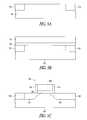
- FIGS. 5A-5Eillustrate an embodiment of a process for forming a metal substituted electrode.
- FIG. 6illustrates a flow diagram of features of an embodiment of a metal substitution technique.
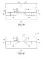
- FIGS. 7A-7Dillustrate an embodiment of a process for forming a self aligned conductive layer.
- FIG. 8illustrates an embodiment of a method for forming a self aligned metal gate on high- ⁇ gate dielectrics containing a hafnium lanthanide oxynitride film.
- FIG. 9illustrates a wafer containing integrated circuits having a hafnium lanthanide oxynitride film.
- FIG. 10shows an embodiment of a transistor having a dielectric layer including a hafnium lanthanide oxynitride film.
- FIG. 11shows an embodiment of a floating gate transistor having a dielectric layer including a hafnium lanthanide oxynitride film.
- FIG. 12shows an embodiment of a capacitor having a dielectric layer including a hafnium lanthanide oxynitride film.
- FIG. 13depicts an embodiment of a dielectric layer having multiple layers including a hafnium lanthanide oxynitride layer.
- FIG. 14is a simplified diagram for an embodiment of a controller coupled to an electronic device having a dielectric layer including a hafnium lanthanide oxynitride film.
- FIG. 15illustrates a diagram for an embodiment of an electronic system including devices with a dielectric film including a hafnium lanthanide oxynitride film.
- wafer and substratemay be used interchangeably to refer generally to any structure on which integrated circuits are formed and also to such structures during various stages of integrated circuit fabrication.
- substrateis understood to include a semiconductor wafer.
- substrateis also used to refer to semiconductor structures during processing and may include other layers that have been fabricated thereupon. Both wafer and substrate include doped and undoped semiconductors, epitaxial semiconductor layers supported by a base semiconductor or insulator, as well as other semiconductor structures well known to one skilled in the art.
- conductoris understood to generally include n-type and p-type semiconductors and the term insulator or dielectric is defined to include any material that is less electrically conductive than the materials referred to as conductors. The following detailed description is, therefore, not to be taken in a limiting sense.
- the dielectric regionshould have a reduced equivalent oxide thickness (t eq ).
- the equivalent oxide thicknessquantifies the electrical properties, such as capacitance, of a dielectric in terms of a representative physical thickness.
- t eqis defined as the thickness of a theoretical SiO 2 layer that would be required to have the same capacitance density as a given dielectric, ignoring leakage current and reliability considerations.
- a SiO 2 layer of thickness, t, deposited on a silicon surfacewill have a t eq larger than its thickness, t.
- This t eqresults from the capacitance in the surface on which the SiO 2 is deposited due to the formation of a depletion/inversion region.
- This depletion/inversion regioncan result in t eq being from 3 to 6 Angstroms ( ⁇ ) larger than the SiO 2 thickness, t.
- the physical thickness requirement for a SiO 2 layer used for a gate dielectricmay need to be approximately 4 to 7 ⁇ . Additional requirements on a SiO 2 layer would depend on the electrode used in conjunction with the SiO 2 dielectric.
- Silicon dioxideis used as a dielectric layer in devices, in part, due to its electrical isolation properties in a SiO 2 —Si based structure. This electrical isolation is due to the relatively large band gap of SiO 2 (8.9 eV), making it a good insulator from electrical conduction. Significant reductions in its band gap may eliminate it as a material for a dielectric region in an electronic device. As the thickness of a SiO 2 layer decreases, the number of atomic layers or monolayers of the material decreases. At a certain thickness, the number of monolayers will be sufficiently small that the SiO 2 layer will not have a complete arrangement of atoms as in a larger or bulk layer.
- a thin SiO 2 layer of only one or two monolayersmay not form a full band gap.
- the lack of a full band gap in a SiO 2 dielectricmay cause an effective short between an underlying electrode and an overlying electrode.
- This undesirable propertysets a limit on the physical thickness to which a SiO 2 layer can be scaled.
- the minimum thickness due to this monolayer effectis thought to be about 7-8 ⁇ . Therefore, for future devices to have a t eq less than about 10 ⁇ , other dielectrics than SiO 2 need to be considered for use as a dielectric region in such future devices.
- materials with a dielectric constant greater than that of SiO 2 , 3.9will have a physical thickness that can be considerably larger than a desired t eq , while providing the desired equivalent oxide thickness.
- an alternative dielectric material with a dielectric constant of 10could have a thickness of about 25.6 ⁇ to provide a t eq of 10 ⁇ , not including any depletion/inversion layer effects.
- a reduced equivalent oxide thickness for transistorscan be realized by using dielectric materials with higher dielectric constants than SiO 2 .
- the thinner equivalent oxide thickness required for lower device operating voltages and smaller device dimensionsmay be realized by a significant number of materials, but additional fabricating requirements make determining a suitable replacement for SiO 2 difficult.
- the current view for the microelectronics industryis still for silicon-based devices. This may require that the dielectric material employed be grown on a silicon substrate or a silicon layer, which places significant constraints on the substitute dielectric material. During the formation of the dielectric on the silicon layer, there exists the possibility that a small layer of SiO 2 could be formed in addition to the desired dielectric. The result would effectively be a dielectric layer consisting of two sublayers in parallel with each other and the silicon layer on which the dielectric is formed. In such a case, the resulting capacitance would be that of two dielectrics in series.
- t eqt SiO 2 +( ⁇ ox / ⁇ ) t.
- SiO 2 as a dielectric layer in a devicehas allowed the formation of a SiO 2 layer that results in an amorphous dielectric.
- Having an amorphous structure for a dielectricprovides for reducing problems of leakage current associated with grain boundaries in polycrystalline dielectrics that provide high leakage paths. Additionally, grain size and orientation changes throughout a polycrystalline dielectric can cause variations in the film's dielectric constant, along with uniformity and surface topography problems.
- Materials having a high dielectric constant relative to SiO 2may also have a crystalline form, at least in a bulk configuration.
- the best candidates for replacing SiO 2 as a dielectric in a deviceare those that can be fabricated as a thin layer with an amorphous form and that have high dielectric constants.
- Capacitor applicationshave used high- ⁇ dielectric materials, which are insulating materials having a dielectric constant greater than silicon dioxide.
- Such high- ⁇ dielectric materialsinclude silicon oxynitride (SiON, ⁇ ⁇ 6), alumina (Al 2 O 3 , ⁇ ⁇ 9), and oxide/nitride composites (SiO 2 /Si 3 N 4 , ⁇ ⁇ 6).
- Other possible candidatesinclude metal oxides ( ⁇ ⁇ 8-80), nitrides ( ⁇ ⁇ 7-30), oxynitrides ( ⁇ ⁇ 6-25), silicates ( ⁇ ⁇ 6-20), carbides ( ⁇ ⁇ 6-15), and complex titanates ( ⁇ ⁇ >100).
- Factors for selecting appropriate materialsinclude physical, chemical and thermal stability as well as etch-ability and stoichiometric reproducibility. In field effect transistor (FET) applications, there are other factors to consider while addressing device scalability.
- the selected dielectricshould provide stable amorphous and adherent films in the thickness range of 1 nm to 100 nm at temperatures ranging from room temperature to 1000° C.
- a relatively defect-free compositionthat is uniform and reproducible with a fixed charge density and trap density of less than 10 11 cm ⁇ 2 in films of such composition is a factor.
- a factorincludes dielectric materials that provide a stable non-reactive interface with a silicon substrate such that the interface has an interface state density much less than 10 11 cm ⁇ 2 .
- Such interface state densitiesmay occur when silicon bonds at the interface are saturated with high strength covalent bonds with molecular elements of the dielectric material.
- Another factordeals with current transport through the dielectric that should be controlled by tunneling, which is independent of temperature, rather than by trap-assisted thermally dependent transport.
- the conductivity of the dielectricshould be equal to or lower than SiO 2 films when voltage is stressed to a field strength of 5 ⁇ 10 6 V/cm.
- a dielectric material having a bandgap greater than 5 eV and having an electron and hole barrier height greater than 2 eV at a silicon interfacemay be considered.
- An additional factor to consideris using dielectric materials with a destructive breakdown strength greater than 6 ⁇ 10 6 V/cm.
- processing characteristicsinclude compatibility with gate material, selective etch-ability, chemical inertness to contaminants, dopant and post processing environments (temperature, pressure, ambients), and intrinsic properties associated with annealing of defects/damages caused by post-processing such as ion-implantation, plasma-radiation, and gate/back-end processing.
- mixed metal oxynitridesare constructed as dielectric films in a variety of electronic devices and systems. Most oxynitrides are thermally stable and can integrate into semiconductor device processing. With nitrogen concentration in an oxynitride film at 30% or higher, such oxynitrides are chemically inert. With processing conditions controlled to provide appropriately low partial pressures of hydrogen and ON ions, oxynitride films with a wide range of nitrogen to oxygen ratio can be deposited over a silicon substrate with low fixed charge and interface states density. On the other hand, charge trapping and transport characteristics are dependent on relative ratio of nitrogen to oxygen content in the constructed film.
- a dielectric layerincludes an oxynitride film having approximately 30 atomic % oxygen and approximately 30-35 atomic % nitrogen. With high enough nitrogen content, oxygen-vacancy induced defects in films is negligible when compared with metal oxides.
- Silicon oxynitridehas been used as a gate dielectric and gate insulator for a non-volatile FET device.
- Aluminum oxynitride (AlON)is expected to have a bandgap greater than 5 eV with a ⁇ value similar to SiON.
- metal oxynitridessuch as ZrON, HfON, LaON, and TaON and other single metal oxynitrides are expected to have a lower bandgap.
- bimetal (or metal/silicon) oxynitridesbased on Si, Al, Hf, La, and Ta are used as dielectric films in a variety of electronic devices and systems. These bimetal oxynitrides may provide a bandgap range from 5 eV to greater than 7 eV.
- bandgapsinclude a bandgap of Si—Al—ON of greater than 7 eV, a bandgap of Si—Hf—ON of about 6.9 eV, a bandgap of Al—Hf—ON of about 6.8 eV, a bandgap of Si—Ta—ON of about 6 eV, a bandgap of Al—Ta—ON of about 6 eV.
- Bimetal oxynitrides Hf—Ta—ON, Hf—La—ON, Al—La—ON, Ta—La—ON, and Si—La—ONare estimated to exhibit significantly lower bandgaps.
- the ⁇ value for Si—Al—ONis estimated at approximately 7 to 8, while the ⁇ values for the other oxynitrides of this group are estimated to be in the range from about 15 to 25.
- a film of hafnium lanthanide oxynitridemay be used as a dielectric layer for application in a variety of electronic devices, replacing the use of silicon oxide to provide a higher dielectric constant.
- the hafnium lanthanide oxynitride filmmay be formed as a hafnium lanthanum oxynitride film.
- one of more lanthanidesmay be used to form a hafnium lanthanide oxynitride film.
- the lanthaniderepresented by the expression Ln, may include one or more elements from the lanthanide group consisting of lanthanum (La), cerium (Ce), praseodymium (Pr), neodymium (Nd), promethium (Pm), samarium (Sm), europium (Eu), gadolinium (Gd), terbium (Tb), dysprosium (Dy), holmium (Ho), erbium (Er), thulium (Tm), ytterbium (Yb), and lutetium (Lu).
- Lalanthanum
- Cecerium
- Prpraseodymium
- Ndneodymium
- promethiumPm
- Smsamarium
- Eueuropium
- Gdgadolinium
- Tbterbium
- Dydysprosium
- Hoholmium
- Ererbium
- Tmthulium
- Yb
- a dielectric layermay be constructed containing hafnium lanthanide oxynitride formed using atomic layer deposition with a metal electrode formed in contact with the dielectric layer.
- the metal electrodemay be formed by atomic layer deposition.
- the metal electrodemay be formed by substituting a desired metal material for a previously disposed substitutable material.
- the metal electrodemay be formed as a self aligned metal electrode on and contacting the dielectric layer.
- the metal electrodemay be formed on the dielectric layer using a previously disposed sacrificial carbon layer on the dielectric layer and sacrificial carbon sidewall spacers adjacent to the sacrificial carbon layer.
- hafnium lanthanide oxynitrideis used herein with respect to a composition that essentially consists of hafnium, lanthanide, oxygen, and nitrogen in a form that may be stoichiometric, non-stoichiometric, or a combination of stoichiometric and non-stoichiometric.
- the lanthanidemay be lanthanum.
- the lanthanidemay be one or more elements from the lanthanide group of elements.
- a hafnium lanthanide oxynitride filmmay also be referred to as a hafnium lanthanide oxygen nitrogen film.
- hafnium lanthanide oxynitridemay be formed substantially as a stoichiometric hafnium lanthanide oxynitride film. In an embodiment, hafnium lanthanide oxynitride may be formed substantially as a non-stoichiometric hafnium lanthanide oxynitride film.
- hafnium lanthanide oxynitridemay be formed substantially as a combination film of non-stoichiometric hafnium lanthanide oxynitride and stoichiometric hafnium lanthanide oxynitride.
- a hafnium lanthanide oxynitride compositionmay be expressed as HfLnON, HfLnON x , Hf x Ln y O z N r , or other equivalent form.
- a hafnium lanthanum oxynitride compositionmay be expressed as HfLaON, HfLaON r , Hf x La y O z N r , or other equivalent form.
- HfLnON or its equivalent formsmay be used to include HfLnON in a form that is stoichiometric, non-stoichiometric, or a combination of stoichiometric and non-stoichiometric hafnium lanthanide oxynitride.
- LnO, LnO z , or its equivalent formsmay be used to include lanthanide oxide in a form that is stoichiometric, non-stoichiometric, or a combination of stoichiometric and non-stoichiometric.
- a hafnium lanthanide oxynitride filmmay be doped with elements or compounds other than hafnium, lanthanide, oxygen, and nitrogen.
- a hafnium lanthanide oxynitride dielectric filmmay be formed using atomic layer deposition (ALD). Forming such structures using atomic layer deposition may allow control of transitions between material layers. As a result of such control, atomic layer deposited hafnium lanthanide oxynitride dielectric films can have an engineered transition with a surface on which it is formed.
- ALDatomic layer deposition
- ALDalso known as atomic layer epitaxy (ALE)
- ALEatomic layer epitaxy
- CVDchemical vapor deposition
- ALDalternatively pulsed-CVD
- gaseous precursorsare introduced one at a time to the substrate surface mounted within a reaction chamber (or reactor). This introduction of the gaseous precursors takes the form of pulses of each gaseous precursor.
- the precursor gasis made to flow into a specific area or region for a short period of time.
- the reaction chambermay be purged with a gas, where the purging gas may be an inert gas.
- the reaction chambermay be evacuated. Between the pulses, the reaction chamber may be purged with a gas and evacuated.
- CS-ALDchemisorption-saturated ALD
- the second pulsing phaseintroduces another precursor on the substrate where the growth reaction of the desired film takes place. Subsequent to the film growth reaction, reaction byproducts and precursor excess are purged from the reaction chamber. With favorable precursor chemistry where the precursors absorb and react with each other aggressively on the substrate, one ALD cycle can be performed in less than one second in properly designed flow type reaction chambers.
- precursor pulse timesrange from about 0.5 sec to about 2 to 3 seconds. Pulse times for purging gases may be significantly longer, for example, pulse times of about 5 to about 30 seconds.
- ALDALD
- the saturation of all the reaction and purging phasesmakes the growth self-limiting.
- This self-limiting growthresults in large area uniformity and conformality, which has important applications for such cases as planar substrates, deep trenches, and in the processing of porous silicon and high surface area silica and alumina powders.
- Atomic layer depositionprovides control of film thickness in a straightforward manner by controlling the number of growth cycles.
- the precursors used in an ALD processmay be gaseous, liquid or solid. However, liquid or solid precursors should be volatile. The vapor pressure should be high enough for effective mass transportation. Also, solid and some liquid precursors may need to be heated inside the atomic layer deposition system and introduced through heated tubes to the substrates. The necessary vapor pressure should be reached at a temperature below the substrate temperature to avoid the condensation of the precursors on the substrate. Due to the self-limiting growth mechanisms of ALD, relatively low vapor pressure solid precursors can be used, though evaporation rates may vary somewhat during the process because of changes in their surface area.
- precursors used in ALDthere are several other characteristics for precursors used in ALD.
- the precursorsshould be thermally stable at the substrate temperature, because their decomposition may destroy the surface control of the ALD method that relies on the reaction of the precursor at the substrate surface. A slight decomposition, if slow compared to the ALD growth, may be tolerated.
- the precursorsshould chemisorb on or react with the surface, though the interaction between the precursor and the surface as well as the mechanism for the adsorption is different for different precursors.
- the molecules at the substrate surfaceshould react aggressively with the second precursor to form the desired solid film. Additionally, precursors should not react with the film to cause etching, and precursors should not dissolve in the film. Using highly reactive precursors in ALD contrasts with the selection of precursors for conventional CVD.
- the by-products in the reactionshould be gaseous in order to allow their easy removal from the reaction chamber. Further, the by-products should not react or adsorb on the surface.
- RS-ALDreaction sequence ALD
- the self-limiting process sequenceinvolves sequential surface chemical reactions.
- RS-ALDrelies on chemistry between a reactive surface and a reactive molecular precursor.
- molecular precursorsare pulsed into the ALD reaction chamber separately.
- a metal precursor reaction at the substratemay be followed by an inert gas pulse to remove excess precursor and by-products from the reaction chamber prior to pulsing the next precursor of the fabrication sequence.
- RS-ALDfilms can be layered in equal metered sequences that may all be identical in chemical kinetics, deposition per cycle, composition, and thickness.
- RS-ALD sequencesgenerally deposit less than a full layer per cycle. Typically, a deposition or growth rate of about 0.25 to about 2.00 ⁇ per RS-ALD cycle may be realized.
- RS-ALDProcessing by RS-ALD provides continuity at an interface avoiding poorly defined nucleating regions that are typical for chemical vapor deposition ( ⁇ 20 ⁇ ) and physical vapor deposition ( ⁇ 50 ⁇ ), conformality over a variety of substrate topologies due to its layer-by-layer deposition technique, use of low temperature and mildly oxidizing processes, lack of dependence on the reaction chamber, growth thickness dependent solely on the number of cycles performed, and ability to engineer multilayer laminate films with a resolution of one to two monolayers.
- RS-ALD processesallow for deposition control on the order of monolayers and the ability to deposit monolayers of amorphous films.
- a sequencerefers to the ALD material formation based on an ALD reaction of a precursor with its reactant precursor.
- forming hafnium nitride from a HfCl 4 precursor and NH 3 , as its reactant precursorincludes a hafnium/nitrogen sequence.
- a reactant precursor that contains nitrogenis used to supply nitrogen.
- a precursor that contains nitrogen and that supplies nitrogen to be incorporated in the ALD composition formedwhich may be used in an ALD process with precursors supplying the other elements in the ALD composition, is referred to as a nitrogen reactant precursor.
- NH 3is a nitrogen reactant precursor.
- an ALD sequence for a metal oxidemay be referenced with respect to the metal and oxygen.
- an ALD sequence for hafnium oxidemay also be referred to as a hafnium/oxygen sequence.
- a reactant precursor that contains oxygenis used to supply the oxygen.
- a precursor that contains oxygen and that supplies oxygen to be incorporated in the ALD composition formedwhich may be used in an ALD process with precursors supplying the other elements in the ALD composition, is referred to as an oxygen reactant precursor.
- water vaporis an oxygen reactant precursor.
- An ALD cyclemay include pulsing a precursor, pulsing a purging gas for the precursor, pulsing a reactant precursor, and pulsing the reactant precursor's purging gas.
- An ALD cyclemay include pulsing a precursor, evacuating the reactant chamber, pulsing a reactant precursor, and evacuating the reactant chamber.
- An ALD cyclemay include pulsing a precursor, pulsing a purging gas for the precursor and evacuating the reactant chamber, pulsing a reactant precursor, and pulsing the reactant precursor's purging gas and evacuating the reactant chamber.
- an ALD sequencemay deal with pulsing a reactant precursor to the substrate surface on which a metal-containing species has been absorbed such that the reactant precursor reacts with the metal-containing species resulting in the deposited metal and a gaseous by-product that can be removed during the subsequent purging/evacuating process.
- an ALD sequencemay deal with reacting a precursor containing the metal species with a substrate surface.
- a cycle for such a metal forming sequencemay include pulsing a purging gas after pulsing the precursor containing the metal species to deposit the metal.
- deposition of a semiconductor materialmay be realized in a manner similar to forming a layer of a metal, given the appropriate precursors for the semiconductor material.
- a cyclemay include a number of sequences to provide the elements of the composition.
- a cycle for an ALD formation of an ABO x compositionmay include sequentially pulsing a first precursor/a purging gas for the first precursor/a first reactant precursor/the first reactant precursor's purging gas/a second precursor/a purging gas for the second precursor/a second reactant precursor/the second reactant precursor's purging gas, which may be viewed as a cycle having two sequences.
- a cyclemay include a number of sequences for element A and a different number of sequences for element B.
- ALD formation of an ABO x compositionuses one precursor that contains the elements A and B, such that pulsing the AB containing precursor followed by its reactant precursor onto a substrate may include a reaction that forms ABO x on the substrate to provide an AB/oxygen sequence.
- a cycle of an AB/oxygen sequencemay include pulsing a precursor containing A and B, pulsing a purging gas for the precursor, pulsing an oxygen reactant precursor to the A/B precursor, and pulsing a purging gas for the reactant precursor.
- a cyclemay be repeated a number of times to provide a desired thickness of the composition.
- a cycle for an ALD formation of the quaternary composition, hafnium lanthanide oxygen nitrogenmay include sequentially pulsing a first precursor/a purging gas for the first precursor/a first reactant precursor/the first reactant precursor's purging gas/a second precursor/a purging gas for the second precursor/a second reactant precursor/the second reactant precursor's purging gas/a third precursor/a purging gas for the third precursor/a third reactant precursor/the third reactant precursor's purging gas, which may be viewed as a cycle having three sequences.
- a layer substantially of a hafnium lanthanide oxynitride compositionis formed on a substrate mounted in a reaction chamber using ALD in repetitive lanthanide/oxygen and hafnium/nitrogen sequences using precursor gases individually pulsed into the reaction chamber.
- a layer substantially of a hafnium lanthanide oxynitride compositionis formed on a substrate mounted in a reaction chamber using ALD in repetitive lanthanide/nitrogen and hafnium/oxygen sequences using precursor gases individually pulsed into the reaction chamber.
- a substantially hafnium lanthanide oxynitride compositionis formed by ALD having approximately 30% nitrogen and 30% oxygen concentrations in the resultant HfLnON dielectric film.
- FIG. 1shows an embodiment of an atomic layer deposition system 100 for processing a dielectric film containing a Hf x Ln y O z N r layer.
- the elements depictedare those elements necessary for discussion of various embodiments for forming HfLnON such that those skilled in the art may practice embodiments of the present invention without undue experimentation.
- a substrate 110is located inside a reaction chamber 120 of ALD system 100 .
- a heating element 130which is thermally coupled to substrate 110 to control the substrate temperature.
- a gas-distribution fixture 140introduces precursor gases to the substrate 110 . Each precursor gas originates from individual gas sources 150 - 155 whose flow is controlled by mass-flow controllers 156 - 161 , respectively.
- Gas sources 150 - 155provide a precursor gas either by storing the precursor as a gas or by providing a location and apparatus for evaporating a solid or liquid material to form the selected precursor gas. Furthermore, additional gas sources may be included, one for each metal precursor employed and one for each reactant precursor associated with each metal precursor.
- purging gas sources 163 , 164are also included in the ALD system.
- additional purging gas sourcesmay be constructed in ALD system 100 , one purging gas source for each precursor gas. For a process that uses the same purging gas for multiple precursor gases, less purging gas sources are required for ALD system 100 .
- Gas sources 150 - 155 and purging gas sources 163 - 164are coupled by their associated mass-flow controllers to a common gas line or conduit 170 , which is coupled to the gas-distribution fixture 140 inside reaction chamber 120 .
- Gas conduit 170is also coupled to vacuum pump, or exhaust pump, 181 by mass-flow controller 186 to remove excess precursor gases, purging gases, and by-product gases at the end of a purging sequence from gas conduit 170 .
- Vacuum pump, or exhaust pump, 182is coupled by mass-flow controller 187 to remove excess precursor gases, purging gases, and by-product gases at the end of a purging sequence from reaction chamber 120 .
- mass-flow controller 187to remove excess precursor gases, purging gases, and by-product gases at the end of a purging sequence from reaction chamber 120 .
- control displays, mounting apparatus, temperature sensing devices, substrate maneuvering apparatus, and necessary electrical connections as are known to those skilled in the artare not shown in FIG. 1 .
- the use, construction and fundamental operation of reaction chambers for deposition of filmsare understood by those of ordinary skill in the art of semiconductor fabrication. Embodiments of the present invention may be practiced on a variety of such reaction chambers without undue experimentation.
- one of ordinary skill in the artwill comprehend the necessary detection, measurement, and control techniques in the art of semiconductor fabrication upon reading the disclosure.
- a hafnium lanthanide oxynitride layermay be structured as one or more monolayers.
- a film of hafnium lanthanide oxynitride, structured as one or more monolayers,may have a thickness that ranges from a monolayer to thousands of angstroms or more.
- the filmmay be processed using atomic layer deposition.
- Embodiments of an atomic layer deposited hafnium lanthanide oxynitride layerhave a larger dielectric constant than silicon dioxide.
- Such dielectric layersprovide a significantly thinner equivalent oxide thickness compared with a silicon oxide layer having the same physical thickness.
- such dielectric layersprovide a significantly thicker physical thickness than a silicon oxide layer having the same equivalent oxide thickness. This increased physical thickness aids in reducing leakage current.
- the surface on which the hafnium lanthanide oxynitride film is to be depositedmay undergo a preparation stage.
- the surfacemay be the surface of a substrate for an integrated circuit.
- the substrate used for forming a transistormay include a silicon or silicon containing material.
- silicon germanium, germanium, gallium arsenide, silicon-on-sapphire substrates, or other suitable substratesmay be used.
- a preparation processmay include cleaning the substrate and forming layers and regions of the substrate, such as drains and sources, prior to forming a gate dielectric in the formation of a metal insulator semiconductor (MIS) transistor.
- MISmetal insulator semiconductor
- active regionsmay be formed after forming the dielectric layer, depending on the over-all fabrication process implemented.
- the substrateis cleaned to provide an initial substrate depleted of its native oxide.
- the initial substrateis cleaned also to provide a hydrogen-terminated surface.
- a silicon substrateundergoes a final hydrofluoric (HF) rinse prior to ALD processing to provide the silicon substrate with a hydrogen-terminated surface without a native silicon oxide layer.
- HFfinal hydrofluoric
- Cleaning immediately preceding atomic layer depositionaids in reducing an occurrence of silicon oxide as an interface between a silicon-based substrate and a hafnium lanthanide oxynitride dielectric formed using the atomic layer deposition process.
- the material composition of an interface layer and its propertiesare typically dependent on process conditions and the condition of the substrate before forming the dielectric layer. Though the existence of an interface layer may effectively reduce the dielectric constant associated with the dielectric layer and its substrate interface layer, a SiO 2 interface layer or other composition interface layer may improve the interface density, fixed charge density, and channel mobility of a device having this interface layer.
- the sequencing of the formation of the regions of an electronic device, such as a transistor, being processedmay follow typical sequencing that is generally performed in the fabrication of such devices as is well known to those skilled in the art. Included in the processing prior to forming a dielectric may be the masking of substrate regions to be protected during the dielectric formation, as is typically performed in semiconductor fabrication. In an embodiment, an unmasked region includes a body region of a transistor; however, one skilled in the art will recognize that other semiconductor device structures may utilize this process.
- a purging gasmay be pulsed into the ALD reaction chamber.
- the ALD reactor chambermay be evacuated using vacuum techniques as is known by those skilled in the art.
- a purging gasmay be pulsed into the ALD reaction chamber and the ALD reactor chamber may be evacuated.
- an ALD cycle for forming HfLnONincludes sequencing component-containing precursors in the order of lanthanide, oxygen, hafnium, and nitrogen with appropriate purging between the different component-containing precursors. Full coverage or partial coverage of a monolayer on a substrate surface may be attained for pulsing of a metal-containing precursor.
- an ALD cycle for forming HflnONincludes sequencing the component-containing precursors in various permutations.
- an ALD cycle to form hafnium lanthanide oxynitrideincludes a number, x, of lanthanide/oxygen sequences and a number, y, of hafnium/nitrogen sequences.
- an ALD cycle to form hafnium lanthanide oxynitrideincludes a number, x, of lanthanide/nitrogen sequences and a number, y, of hafnium/oxygen sequences.
- the number of sequences x and yis selected to engineer the relative amounts of hafnium, lanthanide, oxygen, and nitrogen.
- the number of sequences x and yis selected to form a nitrogen-rich hafnium lanthanide oxynitride.
- the number of sequences x and yare selected to form an oxygen-rich hafnium lanthanide oxynitride.
- the hafnium lanthanide oxynitridemay be engineered as a lanthanide-rich dielectric relative to the amount of hafnium in the dielectric.
- the hafnium lanthanide oxynitridemay be engineered as a hafnium-rich dielectric relative to the amount of lanthanide in the dielectric.
- the pulsing of the individual component-containing precursorsmay be performed independently in a non-overlapping manner using the individual gas sources 150 - 155 and flow controllers 156 - 161 of ALD system 100 of FIG. 1 .
- Each precursormay be pulsed into the reaction chamber for a predetermined period, where the predetermined period can be set separately for each precursor. Additionally, for various ALD formations, each precursor may be pulsed into the reaction chamber under separate environmental conditions.
- the substratemay be maintained at a selected temperature and the reaction chamber maintained at a selected pressure independently for pulsing each precursor. Appropriate temperatures and pressures may be maintained, whether the precursor is a single precursor or a mixture of precursors.
- a number of precursors containing a lanthanidemay be used to provide the lanthanide to a substrate for an integrated circuit.
- a lanthanum-containing precursoris pulsed onto a substrate in an ALD reaction chamber.
- Meis an abbreviation for CH 3
- Etis an abbreviation for ethyl (CH 2 CH 3 )
- Cpis an abbreviation for a cyclopentadienyl ligand having the formula C 5 H 5 .
- H 2may be pulsed along with a La(EtCp) 3 precursor or a La(DPM) 3 precursor to reduce carbon contamination in the fabricated film.
- Other precursorsmay be used in embodiments in which the lanthanide is other than lanthanum.
- a reactant precursormay be pulsed into the reaction chamber.
- the reactant precursormay be an oxygen reactant precursor that may include, but is not limited to, one or more of water, atomic oxygen, molecular oxygen, ozone, hydrogen peroxide, a water—hydrogen peroxide mixture, alcohol, or nitrous oxide.
- the pulsing of the lanthanide precursormay use a pulsing period that provides uniform coverage of a monolayer on the surface or may use a pulsing period that provides partial coverage of a monolayer on the surface during a lanthanide sequence.
- a number of precursors containing hafniummay be used to provide the hafnium to a substrate for an integrated circuit.
- a precursor containing hafniummay include anhydrous hafnium nitride, Hf(NO 3 ) 4 .
- the substrate temperaturemay be maintained at a temperature ranging from about 160° C. to about 180° C.
- a hafnium precursormay include HfCl 4 .
- the substrate temperaturemay be maintained at a temperature ranging from about 180° C. to about 600° C.
- the substrate temperaturemay be maintained at a temperature ranging from about 300° C. to about 940° C.
- a hafnium precursormay be HfI 4 .
- the substrate temperaturemay be maintained at a temperature of about 300° C.
- Hafnium oxidemay be grown by ALD using a Hf[N(CH 3 )(C 2 H 5 )] 4 , which may be known as a homoleptic tetrakis(dialkylamino) hafnium(IV) compound, and water as an oxygen reactant.
- hafnium tetrakis(dialkylamino) hafnium compoundsmay also be used, such as hafnium tetrakis dimethylamine, Hf[N(CH 3 ) 2 ] 4 , or hafnium tetrakis diethylamine, Hf[N(C 2 H 5 ) 2 ] 4 , as a hafnium-containing precursor.
- hafnium tetrakis dimethylamineHf[N(CH 3 ) 2 ] 4
- hafnium tetrakis diethylamineHf[N(C 2 H 5 ) 2 ] 4
- use of the individual hafnium-containing precursorsis not limited to the temperature ranges of the above example embodiments.
- the pulsing of the hafnium precursormay use a pulsing period that provides uniform coverage of a monolayer on the surface or may use a pulsing period that provides partial coverage of a monolayer on the surface during a hafnium sequence.
- nitrogenmay be used as a purging gas and a carrier gas for one or more of the sequences used in the ALD formation of hafnium lanthanide oxynitride.
- hydrogen, argon gas, or other inert gasesmay be used as the purging gas.
- Excess precursor gas and reaction by-productsmay be removed by the purge gas.
- Excess precursor gas and reaction by-productsmay be removed by evacuation of the reaction chamber using various vacuum techniques.
- Excess precursor gas and reaction by-productsmay be removed by the purge gas and by evacuation of the reaction chamber.
- the thickness of a hafnium lanthanide oxynitride layer formed by atomic layer depositionis determined by a fixed growth rate for the pulsing periods and precursors used, set at a value such as N nm/cycle, and the number of cycles conducted.
- the processis conducted in an ALD window, which is a range of temperatures in which the growth rate is substantially constant. In an embodiment, if such an ALD window is not available, the ALD process is conducted at the same set of temperatures for each ALD sequence in the process. For a desired hafnium lanthanide oxynitride layer thickness, t, in an application, the ALD process is repeated for t/N total cycles. Once the t/N cycles have completed, no further ALD processing for the hafnium lanthanide oxynitride layer is required. In an embodiment, a hafnium lanthanide oxynitride layer processed at relatively low temperatures associated with atomic layer deposition provides an amorphous layer.
- a HfLnON filmmay be grown to a desired thickness by repetition of a process including atomic layer deposition of layers of LnO and HfN and/or layers of HfO and LnN followed by annealing.
- a base thicknessmay be formed according to various embodiments such that forming a predetermined thickness of a HfLnON film may be conducted by forming a number of layers having the base thickness. As can be understood by one skilled in the art, determining the base thickness depends on the application and can be determined during initial processing without undue experimentation.
- Relative amounts of hafnium, lanthanide, oxygen, and nitrogen in a HfLnON filmmay be controlled by regulating the relative thicknesses of the individual layers of oxides and nitrides formed.
- relative amounts of hafnium, lanthanide, oxygen, and nitrogen in a HfLnON filmmay be controlled by forming a layer of HfLnON as multiple layers of different base thickness and by regulating the relative thicknesses of the individual layers of oxides and nitrides formed in each base layer prior to annealing.
- FIG. 2Ashows a flow diagram of features of an embodiment for forming HfLnON using atomic layer deposition and nitridization.
- a layer of HfLnOis formed using atomic layer deposition.
- the layer of HfLnOis subjected to a nitridization to form a HfLnON film.
- the nitridizationmay be a high temperature nitridization.
- active nitrogenmay be introduced by microwave plasma.
- active nitrogenmay be introduced by a NH 3 anneal.
- a high temperature nitridizationis a nitridizing process that is performed at temperatures equal to or above 500° C.
- HfLnOmay be formed by atomic layer deposition using ALD cycles of lanthanide/oxygen sequences and hafnium/oxygen sequences.
- the ALD cyclecan be selected from a number of different permutations of lanthanide/oxygen sequences and hafnium/oxygen sequences.
- FIG. 2Bshows a flow diagram of features of an embodiment for forming HfLnO using atomic layer deposition for nitridization to a HfLnON film.
- a layer of lanthanide oxideis formed on a substrate by atomic layer deposition.
- a layer of hafnium oxideis formed by atomic layer deposition on the layer of lanthanide oxide.
- the layers of lanthanide oxide and hafnium oxideare annealed to form a layer of HfLnO.
- the order of forming LnO and HfOmay be interchanged.
- the layer of HfLnOmay be nitridized to form HfLnON.
- the layers of lanthanide oxide and hafnium oxidemay be nitridized during the annealing process.
- alternating layers of ALD lanthanide oxide and ALD hafnium oxidemay be formed to a desired thickness prior to nitridization.
- a layer of ALD lanthanide oxide and a layer of ALD hafnium oxidemay be formed, each to a desired thickness, the layers of ALD lanthanide oxide and ALD hafnium oxide nitridized to form a HfLnON layer.
- a layer of ALD lanthanide oxide and a layer of ALD hafnium oxidemay be formed on the HfLnON layer, the layers of ALD lanthanide oxide and ALD hafnium oxide nitridized to form a HfLnON layer on and contiguous with the previously formed HfLnON layer. This process may be continued until the desired thickness of HfLnON is formed.
- ALD LaOmay be formed using a number of precursors containing lanthanum to provide the lanthanum to a substrate for an integrated circuit.
- lanthanum-containing precursorsinclude, but are not limited to, La(thd) 3 , tris (2,2,6,6-tetramethyl-3,5-heptanedionato)lanthanum (III) tetraglyme adduct, La(EtCp) 3 , and La(DPM) 3 .
- the oxygen reactant precursormay include, but is not limited to, one or more of water, atomic oxygen, molecular oxygen, ozone, hydrogen peroxide, a water—hydrogen peroxide mixture, alcohol, or nitrous oxide.
- the reaction chambermay be purged of excess precursor and by-products.
- the pulsing of the precursorsmay use pulsing periods that provide uniform coverage of a monolayer on the surface or may use pulsing periods that provide partial coverage of a monolayer on the surface during a lanthanum/oxygen ALD cycle.
- ALD HfOmay be formed using a number of precursors containing hafnium to provide the hafnium to a substrate for an integrated circuit.
- hafnium-containing precursorsinclude, but are not limited to, a hafnium halide, such as HfCl 4 and HfI 4 , Hf(NO 3 ) 4 , Hf[N(CH 3 )(C 2 H 5 )] 4 , Hf[N(CH 3 ) 2 ] 4 , and Hf[N(C 2 H 5 ) 2 ] 4 .
- an oxygen reactant precursormay be pulsed into the reaction chamber.
- the oxygen reactant precursormay include, but is not limited to, one or more of water, atomic oxygen, molecular oxygen, ozone, hydrogen peroxide, a water—hydrogen peroxide mixture, alcohol, or nitrous oxide.
- the pulsing of the precursorsmay use pulsing periods that provide uniform coverage of a monolayer on the surface or may use pulsing periods that provide partial coverage of a monolayer on the surface during a during an ALD cycle forming HfO.
- nitrogenmay be used as a purging gas and a carrier gas for one or more of the sequences.
- hydrogen, argon gas, or other inert gasesmay be used as the purging gas.
- Excess precursor gas and reaction by-productsmay be removed by the purge gas.
- Excess precursor gas and reaction by-productsmay be removed by evacuation of the reaction chamber using various vacuum techniques.
- Excess precursor gas and reaction by-productsmay be removed by the purge gas and by evacuation of the reaction chamber.
- FIG. 3shows a flow diagram of features of an embodiment for forming HfLnON using atomic layer deposition and oxidation.
- a layer of HfNis formed by atomic layer deposition.
- a layer of LnNis formed by atomic layer deposition on the layer of HfN.
- HfN and LnN filmsmay be alternately deposited in adjacent layers, in which either nitride layer may be deposited as the starting layer.
- the layers of LnN and HfNare annealed.
- the annealed layers of LnN and HfNare oxidized to form HfLnON. In an embodiment, the annealing and oxidation may be performed together.
- the layers of LnN and HfNmay be annealed and oxidized by rapid thermal oxidation to form HfLnON.
- ALD HfNmay be formed using a number of precursors containing hafnium to provide the hafnium to a substrate for an integrated circuit.
- a hafnium-containing precursoris pulsed onto a substrate in an ALD reaction chamber.
- a number of precursors containing hafniummay be used to provide the hafnium to a substrate for an integrated circuit.
- the hafnium-containing precursormay be a hafnium halide precursor, such as HfCl 4 or HfI 4 .
- the hafnium nitridemay be grown by ALD using Hf[N(CH 3 )(C 2 H 5 )] 4 .
- the substratemay be held at a temperature ranging from about 150° C. to about 300° C.
- Other types of tetrakis(dialkylamino) metal compoundsmay also be used, such as hafnium tetrakis dimethylamine, Hf[N(CH 3 ) 2 ] 4 , or hafnium tetrakis diethylamine, Hf[N(C 2 H 5 ) 2 ] 4 , as a hafnium-containing precursor.
- a reactant precursormay be pulsed into the reaction chamber.
- the reactant precursormay be a nitrogen reactant precursor including, but not limited to, ammonia (NH 3 ).
- Other nitrogen reactant precursors that may be usedinclude nitrogen-containing compositions that do not include oxygen.
- use of the individual hafnium-containing precursorsis not limited to the temperature ranges of the above embodiments. Further, forming hafnium nitride by atomic layer deposition is not limited to the abovementioned precursors.
- the pulsing of the hafnium precursormay use a pulsing period that provides uniform coverage of a monolayer on the surface or may use a pulsing period that provides partial coverage of a monolayer on the surface during a hafnium sequence.
- ALD LaNmay be formed using a number of precursors containing lanthanum to provide the lanthanum to a substrate for an integrated circuit.
- lanthanum-containing precursorsinclude, but are not limited to, La(thd) 3 , tris (2,2,6,6-tetramethyl-3,5-heptanedionato)lanthanum (III) tetraglyme adduct, La(EtCp) 3 , and La(DPM) 3 .
- the substratemay be maintained at a temperature ranging from 180° C. to about 425° C.
- H 2may be pulsed along with the La(EtCp) 3 precursor or the precursor to reduce carbon contamination in the deposited film.
- a reactant precursormay be pulsed into the reaction chamber.
- a nitrogen reactant precursoris pulsed.
- a number of precursors containing nitrogenmay be used to provide nitrogen.
- nitrogen-containing precursorsinclude, but are not limited to, nitrogen, ammonia (NH 3 ), tert-butylamine (C 4 H, N), allylamine (C 3 H 7 N), 1,1-dimethylhydrazine ((CH 3 ) 2 NNH 2 ).
- the substrateis maintained at a temperature ranging from about 400° C. to about 500° C. using tert-butylamine or allylamine as a nitrogen precursor.
- NH 3may be pulsed with the tert-butylamine and the allylamine. The addition of NH 3 may enhance the deposition rate at lower temperatures.
- use of the individual lanthanum-containing precursorsis not limited to the temperature ranges of the above example embodiments. Further, forming lanthanum nitride by atomic layer deposition is not limited to the abovementioned precursors.
- the pulsing of the lanthanum precursormay use a pulsing period that provides uniform coverage of a monolayer on the surface or may use a pulsing period that provides partial coverage of a monolayer on the surface during a lanthanum/nitrogen sequence.
- nitrogenmay be used as a purging gas and a carrier gas for one or more of the sequences.
- hydrogen, argon gas, or other inert gasesmay be used as the purging gas.
- Excess precursor gas and reaction by-productsmay be removed by the purge gas.
- Excess precursor gas and reaction by-productsmay be removed by evacuation of the reaction chamber using various vacuum techniques.
- Excess precursor gas and reaction by-productsmay be removed by the purge gas and by evacuation of the reaction chamber.
- FIG. 4shows a flow diagram of features of an embodiment for forming HfLnON using atomic layer deposition and annealing.
- a layer of HfONis formed using atomic layer deposition.
- a layer of LnONis formed using atomic layer deposition on the layer of HfON.
- the layers of HfON and LnONare annealed to form a layer of HfLnON.
- HfON and LnON filmsmay be alternately deposited in adjacent layers, in which either oxynitride layer may be deposited as the starting layer.
- ALD LaONmay be formed using a number of precursors containing lanthanum to provide the lanthanum to a substrate for an integrated circuit.
- lanthanum-containing precursorsinclude, but are not limited to, La(thd) 3 , tris (2,2,6,6-tetramethyl-3,5-heptanedionato)lanthanum (III) tetraglyme adduct, La(EtCp) 3 , and La(DPM) 3 .
- a number of precursors containing nitrogenmay be used to provide nitrogen.
- nitrogen-containing precursorsinclude, but are not limited to, nitrogen, ammonia (NH 3 ), tert-butylamine (C 4 H 11 N), allylamine (C 3 H 7 N), 1,1-dimethylhydrazine ((CH 3 ) 2 NNH 2 ).
- an oxygen reactant precursormay be pulsed into the reaction chamber.
- the oxygen reactant precursormay include, but is not limited to, one or more of water, atomic oxygen, molecular oxygen, ozone, hydrogen peroxide, a water—hydrogen peroxide mixture, alcohol, or nitrous oxide.
- the order of pulsing the precursorsmay vary. In various embodiments, forming lanthanum oxynitride by atomic layer deposition is not limited to the abovementioned precursors.
- the pulsing of the precursorsmay use pulsing periods that provide uniform coverage of a monolayer on the surface or may use pulsing periods that provide partial coverage of a monolayer on the surface during an ALD cycle forming LaON.
- ALD HfONmay be formed using a number of precursors containing hafnium to provide the hafnium to a substrate for an integrated circuit.
- hafnium-containing precursorsinclude, but are not limited to, a hafnium halide, such as HfCl 4 or HfI 4 , Hf[N(CH 3 )(C 2 H 5 )] 4 , hafnium tetrakis dimethylamine, Hf[N(CH 3 ) 2 ] 4 , or hafnium tetrakis diethylamine, Hf[N(C 2 H 5 ) 2 ] 4 .
- hafnium halidesuch as HfCl 4 or HfI 4 , Hf[N(CH 3 )(C 2 H 5 )] 4 , hafnium tetrakis dimethylamine, Hf[N(CH 3 ) 2 ] 4 , or hafnium tetrakis diethylamine, Hf[
- a nitrogen reactant precursormay be pulsed into the reaction chamber.
- a number of precursors containing nitrogenmay be used to provide nitrogen.
- NH 3may be used as the nitrogen-containing precursor.
- Other nitrogen reactant precursors that may be usedinclude nitrogen-containing compositions that do not include oxygen.
- the nitrogen-containing precursormay also include oxygen.
- an oxygen reactant precursormay be pulsed into the reaction chamber.
- the oxygen reactant precursormay include, but is not limited to, one or more of water, atomic oxygen, molecular oxygen, ozone, hydrogen peroxide, a water—hydrogen peroxide mixture, alcohol, or nitrous oxide.
- the order of pulsing the precursorsmay vary. Further, forming hafnium oxynitride by atomic layer deposition is not limited to the abovementioned precursors.
- the pulsing of the precursorsmay use pulsing periods that provide uniform coverage of a monolayer on the surface or may use pulsing periods that provide partial coverage of a monolayer on the surface during an ALD cycle forming HfON.
- nitrogenmay be used as a purging gas and a carrier gas for one or more of the sequences.
- hydrogen, argon gas, or other inert gasesmay be used as the purging gas.
- Excess precursor gas and reaction by-productsmay be removed by the purge gas.
- Excess precursor gas and reaction by-productsmay be removed by evacuation of the reaction chamber using various vacuum techniques.
- Excess precursor gas and reaction by-productsmay be removed by the purge gas and by evacuation of the reaction chamber.
- a dielectric stack containing a HfLnON x filmincludes a silicon oxide layer.
- the dielectric layeris formed as a nanolaminate.
- An embodiment of a nanolaminateincludes a layer of a hafnium oxide and a HfLnON x film, a layer of hafnium oxynitride and a HfLnON x film, a layer of lanthanide oxide and a HfLnON x film, a layer of lanthanide oxynitride and a HfLnON x film, layers of hafnium oxide, lanthanide oxide, hafnium oxynitride, and lanthanide oxynitride along with a HfLnON x film, or various other combinations.
- a dielectric layeris formed substantially as the hafnium lanthanide oxynitride film.
- the structure of an interface between a dielectric layer and a substrate on which it is disposedis controlled to limit the inclusion of silicon oxide, since a silicon oxide layer would reduce the effective dielectric constant of the dielectric layer.
- the material composition and properties for an interface layerare dependent on process conditions and the condition of the substrate before forming the dielectric layer.
- the interface layersuch as a silicon oxide interface layer or other composition interface layer, may improve the interface density, fixed charge density, and channel mobility of a device having this interface layer.
- a hafnium lanthanide oxynitride layeris doped with other elements.
- the dopingmay be employed to enhance the leakage current characteristics of the dielectric layer containing the HfLnON x film by providing a disruption or perturbation of the hafnium lanthanide oxynitride structure.
- such dopingis realized by substituting a sequence of one of these elements for a hafnium sequence, a lanthanide sequence, or various combinations of sequences. The choice for substitution may depend on the form of the hafnium lanthanide oxynitride structure with respect to the relative amounts of hafnium atoms and lanthanide atoms desired in the oxide.
- the amount of dopants inserted into the oxynitrideare limited to a relatively small fraction of the total number of hafnium and lanthanide atoms.
- the other materialmay be formed upon the hafnium lanthanide oxynitride layer.
- the other materialis a conductive material.
- the conductive materialmay be used as an electrode. Such electrodes may be used as capacitor electrodes, control gates in transistors, or floating gates in floating gate transistors.
- the conductive materialis a metal or conductive metal nitride.
- the conductive materialis a conductive semiconductor material.
- the conductive materialis formed by ALD processes.
- the conductive materialis formed by a substitution process.
- the conductive materialis formed in a self-alignment process.
- a conductive layermay be deposited by atomic layer deposition on a layer of HfLnON or on a dielectric layer containing a layer of HfLnON.
- a metal layermay be deposited by atomic layer deposition in an ALD cycle having a halide precursor containing the metal to be deposited and a reactant precursor containing hydrogen.
- Metal layer formation by ALDis not limited to halide precursors and hydrogen reactant precursors.
- precursorsmay be selected to form ALD conductive layers such as aluminum (Al), tungsten (W), molybdenum (Mo), gold (Au), silver (Ag), gold alloy, silver alloy, copper (Cu), platinum (Pt), rhenium (Re), ruthenium (Ru), rhodium (Rh), nickel (Ni), osmium (Os), palladium (Pd), iridium (Ir), cobalt (Co), germanium (Ge), or metallic nitrides such as WN, TiN or TaN. Formation of ALD conductive layers is not limited to the abovementioned materials.
- a tantalum layermay be formed on a HfLnON film by atomic layer deposition using a tantalum-containing precursor.
- a tantalum halide precursormay be used with hydrogen as a reactant precursor.
- a TaCl 5 precursormay be used with an atomic hydrogen reactant precursor.
- the atomic hydrogen reactant precursormay be provided using a plasma.
- the substrate temperaturemay be held at a temperature ranging from about 250° C. to about 400° C. The hydrogen reactant precursor reacts at the substrate to remove the halogen, which forms the selected tantalum halide precursor, leaving tantalum on the substrate surface.
- the reaction chambermay be purged of excess precursor and/or by-products.
- use of the individual tantalum-containing precursorsis not limited to the temperature ranges of the above example embodiments.
- forming tantalum by atomic layer depositionis not limited to the abovementioned precursors.
- the pulsing of the tantalum precursormay use a pulsing period that provides uniform coverage of a monolayer on the surface or may use a pulsing period that provides partial coverage of a monolayer on the surface.
- the tantalum layermay be structured as one or more monolayers.
- the tantalum layermay have a thickness ranging from a monolayer to thousands of angstroms or more.
- a metal nitride layermay be deposited by atomic layer deposition using a precursor containing the metal to be deposited and a reactant precursor containing nitrogen in an ALD cycle.
- a titanium nitride layermay be formed with a HfLnON film by atomic layer deposition using a titanium-containing precursor.
- a nitrogen-containing precursormay be used as the reactant precursor for the titanium-containing precursor.
- the titanium-containing precursor and the nitrogen-containing precursormay be selected such that their use does not form a titanium oxide in the layer of titanium nitride being formed.
- the titanium-containing precursor and the nitrogen-containing precursormay be selected such that these precursors do not include oxygen as an elemental component.
- a titanium halide precursormay be used with NH 3 as a reactant precursor.
- a TiCl 4 precursormay be used with a NH 3 reactant precursor.
- the substrate temperaturemay be held at a temperature ranging from about 380° C. to about 500° C. In an embodiment, the substrate temperature may be held at a temperature less than 600° C. After pulsing a titanium-containing precursor and after pulsing its reactant precursor, the reaction chamber may be purged of excess precursor and/or by-products. In various embodiments, use of the individual titanium-containing precursors is not limited to the temperature ranges of the above example embodiments.
- titanium nitride by atomic layer depositionis not limited to the abovementioned precursors, but may include precursors containing oxygen.
- the pulsing of the titanium precursormay use a pulsing period that provides uniform coverage of a monolayer on the surface or may use a pulsing period that provides partial coverage of a monolayer on the surface.
- the titanium nitride layermay be structured as one or more monolayers.
- the titanium nitride layermay have a thickness ranging from a monolayer to thousands of angstroms or more.
- FIGS. 5A-5Eillustrate an embodiment of a process for forming a metal substituted electrode in place of a previously deposited material on a dielectric containing HfLnON. Though a transistor is discussed with reference to FIGS. 5A-5E , such a process may be used with respect to other embodiments of device configurations.
- FIG. 5Ashows a substrate 501 and shallow trench isolation (STI) regions 502 .
- the substrate 501can be a semiconductor wafer as well as structures having one or more insulative, semi-insulative, conductive, or semiconductive layers and materials.
- the substratecan include silicon-on-insulator, silicon-on-sapphire, and other structures upon which semiconductor devices are formed.
- FIG. 5Bfurther shows a gate dielectric layer 503 formed on the substrate 501 , and a gate substitutable layer 504 formed on the gate dielectric layer 503 .
- the gate dielectric layermay include a dielectric layer containing HfLnON in addition to other insulative material or a dielectric layer essentially of HfLnON. The use of such a high- ⁇ dielectric increases the capacitance, which is useful for nanoscale integrated circuits.
- the gate dielectricincludes stacked layers comprising one or more high- ⁇ dielectric materials.
- the material of the gate substitutable layer 504is selected with respect to the desired gate material to allow the gate material to replace the gate substitutable layer. This process forms a gate of the desired gate metal where the substitutable material was positioned on the gate dielectric.
- Source/drain regions 507are also formed. Source/drain regions 507 can be formed using conventional ion implantation and subsequent annealing. These annealing temperatures can pose problems for aluminum gates and other metal gates that have melting temperatures less than the anneal temperature for the source/drain regions.
- FIG. 5Dshows an insulative fill layer 508 provided to match the thickness of the gate stack.
- a planarization proceduresuch as chemical-mechanical polishing, can be used to provide an even surface across the fill layer 508 and the gate substitutable layer 504 .
- a metal layer 509formed of material intended to be the gate material, is deposited over the gate substitutable layer 504 and the fill layer 508 .
- the metal layer 509is also referred to herein as a layer of gate material.
- Various deposition processessuch as evaporation, sputtering, chemical vapor deposition, or atomic layer deposition, may be used to form the metal layer 509 .
- the volume of layer 509is significantly larger than the volume of the substitutable material left on the wafer.
- a metal-substitution reactionis induced.
- the reactioncan be provided by annealing the structure in a non-oxidizing atmosphere such as a nitrogen gas or a forming gas. The heating urges diffusion or dissolution of the intended gate material in metal layer 509 for the substitutable material 504 .
- the substitution processis bounded by the spacers 506 and the gate dielectric 503 .
- FIG. 5Eshows the resulting low-resistance gate structure.
- the illustrated structureincludes a metal substituted gate 510 formed by the substitution of the metal of layer 509 .
- the metal substituted gate 510may include a small amount of the gate substitutable material that did not diffuse above the planarization level 511 . Such small amounts of the gate substitutable material do not significantly affect the conductivity of the metal substituted gate 510 , and thus do not significantly affect the performance of the device.
- Drain and source contactscan be formed, as well as interconnects to other transistors or components, using conventional techniques. Another heat treatment may occur after packaging the integrated circuit in a protective housing in an attempt to reduce the resistivity of the metal gate contacts and other metal interconnections.
- the metal gate substitution techniquecan be applied to MOS devices, as generally illustrated in FIG. 5E , as well as to form metal floating gates and/or metal control gates in nonvolatile devices. Additionally, various high- ⁇ dielectrics having a HfLnON film can be used between the floating gate and the substrate, and between the control gate and the floating gate in these nonvolatile devices.
- FIG. 6illustrates a flow diagram of features of an embodiment of a metal substitution technique.
- a gate dielectricis formed on a substrate.
- the gate dielectricincludes a HfLnON film.
- a layer of gate substitutable materialis formed on the gate dielectric. Examples of gate substitutable material include polysilicon, germanium, silicon-germanium, and carbon.
- source/drain regionsare formed.
- a layer of gate materialis formed at 615 on the gate substitutable material. Examples of such metals include gold, silver, and aluminum. Other metals may be used.
- the gate materialis substituted for the layer of gate substitutable material.
- a metal substitution reactionsubstitutes or replaces the substitutable material (e.g. silicon, germanium, silicon-germanium, carbon) with a metal. After the substitution, the resulting gate structure includes substantially all of the desired metal. Small amounts of the substitutable material may remain in the gate structure.
- the substitution reactioncan be induced by heating the integrated circuit assembly to a desired temperature in a vacuum, nitrogen, argon, forming gas or other non-oxidizing atmosphere. Heating causes diffusion of the metal layer 609 into the substitutable layer.
- the annealing temperature for the substitutionis less than the eutectic (lowest melting) temperature of materials involved in the substitution for the reaction for substitution to occur.
- a metal layermay be formed from gold and annealed at approximately 300° C.
- a metal layermay be formed from silver and annealed at approximately 500-600° C. to substitute the silver for a silicon substitutable structure.
- a polysilicon and germanium substitutable materialmay be used, which reduces the anneal temperature.
- the gate substitutable material 504 shown in FIGS. 5A-5Eincludes polysilicon.
- the gate substitutable materialincludes germanium.
- Some embodimentsuse silicon-germanium with a percentage of silicon in the range from 0% to 100% as the gate substitutable material 504 .
- Some embodimentsuse carbon as the gate substitutable material 504 .
- a replacement metal for the substituted gatemay include aluminium, silver, gold, an alloy of silver, an alloy of gold as the replacement metal, or combinations thereof.
- a replacement metal for the substituted gatemay include gold, silver, an alloy of gold, an alloy of silver, copper, platinum, rhenium, ruthenium, rhodium, nickel, osmium, palladium, iridium, cobalt, germanium, or combinations thereof.
- Various embodimentsform an integrated circuit structure using two or more substitution reactions. Relatively higher temperature substitution processes can be performed before relatively lower temperature substitution processes.
- One application for multiple substitution reactionsis to independently adjust work functions of NMOS and PMOS transistors in CMOS integrated circuits. Multiple substitution reactions are not limited to this CMOS integrated circuit application. Additional information regarding metal substitution can be found in U.S. patent application Ser. No. 11/176,738 filed Jul. 7, 2005, entitled “METAL-SUBSTITUTED TRANSISTOR GATES,” which is herein incorporated by reference.
- FIGS. 7A-7Dillustrate an embodiment of a process for forming a self aligned conductive layer such as a metal gate for a transistor structure.
- FIG. 7 Aillustrates a high- ⁇ gate dielectric 710 containing HfLnON formed on a substrate 701 .
- the substrate 701can be a semiconductor wafer as well as structures having one or more insulative, semi-insulative, conductive, or semiconductive layers and materials.
- the substratecan include silicon-on-insulator, silicon-on-sapphire, and other structures upon which semiconductor devices are formed.
- a sacrificial gate 703is formed of amorphous carbon on the high- ⁇ gate dielectric 710 .
- an etch barrier 708is formed over the sacrificial gate and the dielectric.
- the etch barrier 708includes silicon nitride or aluminium oxide, and can be formed using a deposition process, according to various embodiments.
- Sacrificial sidewall spacers 706are added adjacent the sacrificial gate 703 .
- the spacers 706are formed of amorphous carbon by deposition and conventional direct etch techniques.
- An ion implantation 730 and high temperature annealare used to form source/drain regions 702 in areas defined by the sacrificial sidewall spacers 706 . These annealing temperatures can pose problems for aluminum gates and other metal gates that have melting temperatures less than the anneal temperature for the source/drain regions.
- FIG. 7Bthe sacrificial sidewall spacers ( 706 in FIG. 7A ) have been removed.
- Various embodimentsuse a plasma oxidation process to remove the sacrificial sidewall spacers.
- the etch barrier ( 708 in FIG. 7A )has been removed.
- a light dose ion implantation 740is used to form source/drain extensions 742 in the substrate 701 .
- the extensions 742can be annealed at lower temperatures and in shorter times than the more heavily doped source/drain regions 702 .
- source/drain extensions for the transistormay be formed with doping the substrate to a depth of 30 nm or less.
- conventional or non-carbon sidewall spacers 756are formed and the whole structure is back filled with an oxide fill 758 , such as silicon dioxide, and planarized.
- oxide fill 758such as silicon dioxide
- the conventional sidewall spacersare formed with silicon nitride.
- the sacrificial gate( 703 in FIG. 7C ) is removed and replaced by the deposition of a metal layer 760 .
- the sacrificial gateis removed using a plasma oxidation process.
- Various deposition processessuch as evaporation, sputtering, chemical vapor deposition, or atomic layer deposition, may be used to form the metal layer 760 .
- the structureis planarized (not shown) using a planarization procedure, such as chemical-mechanical polishing, resulting in the self aligned metal gate over the high- ⁇ gate dielectric insulator 710 .
- Drain and source contacts(not shown) can be formed, as well as interconnects to other transistors or components, using conventional techniques. Another heat treatment may occur after packaging the integrated circuit in a protective housing in an attempt to reduce the resistivity of the metal gate contacts and other metal interconnections.
- FIGS. 7A-7Dillustrate two replacement processes for the formation of planar self aligned metal gate transistors, one for disposable sidewall spacers and the other for the gate material itself.
- the metal gate replacement techniqueas disclosed herein, can be applied to MOS devices, as generally illustrated in FIGS. 7A-7D , as well as to form metal floating gates and/or metal control gates in nonvolatile devices. Additionally, various high- ⁇ dielectrics can be used between the floating gate and the substrate, and between the control gate and the floating gate in these nonvolatile devices.
- FIG. 8illustrates an embodiment of a method 800 for forming a self aligned metal gate on high- ⁇ gate dielectrics containing HfLnON.
- a high- ⁇ gate dielectric containing HfLnONis formed on a substrate, at 802 .
- a sacrificial carbon gateis formed on the gate dielectric.
- sacrificial carbon sidewall spacersare formed adjacent to the sacrificial carbon gate.
- source/drain regions for the transistorare formed, using the sacrificial carbon sidewall spacers to define the source/drain regions.
- the sacrificial carbon sidewall spacersare replaced with non-carbon sidewall spacers at 810 .
- the sacrificial carbon gateis replaced with a desired metal gate material to provide the desired metal gate material on the gate dielectric.
- source/drain extensionsmay be formed after removing the carbon sidewall spacers and before replacing with non-carbon sidewall spacers.
- An etch barrieris used in various embodiments to separate the sacrificial carbon gate from the sacrificial carbon sidewall spacers.
- the carbon sacrificial gatemay be replaced with aluminum (Al), tungsten (W), molybdenum (Mo), gold (Au), silver (Ag), gold alloy, silver alloy, copper (Cu), platinum (Pt), rhenium (Re), ruthenium (Ru), rhodium (Rh), nickel (Ni), osmium (Os), palladium (Pd), iridium (Ir), cobalt (Co), germanium (Ge), or metallic nitrides such as WN, TiN or TaN covered by metals.
- the high- ⁇ gate dielectric formed at 802may be one of a number of high- ⁇ gate dielectrics containing HfLnON.
- construction of an integrated circuit structureincludes a dielectric containing HfLnON on which is disposed a self-aligned metal electrode. Additional information regarding a self-aligned metal electrode used as a transistor gate can be found in U.S. patent application Ser. No. 11/216,375, filed 31 Aug. 2005, entitled “SELF ALIGNED METAL GATES ON HIGH-K DIELECTRICS,” which is herein incorporated by reference.
- FIG. 9illustrates an embodiment of a wafer 940 containing integrated circuits having one or more dielectric layers that include a hafnium lanthanide oxynitride film.
- Conductive electrodesmay be disposed on such dielectrics in a number of configurations such as capacitors, transistors, or elements of a memory.
- the conductive electrodesmay be metal electrodes, conductive metal nitride electrodes, and/or conductive metal oxide electrodes.
- the conductive electrodesmay be atomic layer deposited electrodes.
- Metal electrodesmay be metal substituted electrodes and/or self aligned metal electrodes formed in accordance with the teachings of embodiments discussed herein.
- a common wafer sizeis 8 inches in diameter.
- wafersare capable of being fabricated in other sizes, and embodiments of wafers containing a hafnium lanthanide oxynitride film are not limited to a particular size.
- a number of diescan be formed on a wafer.
- a die 941is an individual pattern on a substrate that contains circuitry to perform a specific function.
- a semiconductor wafertypically contains a repeated pattern of such dies containing the same functionality.
- a dieis typically packaged in a protective casing (not shown) with leads extending therefrom (not shown) providing access to the circuitry of the die for communication and control.
- Applications containing electronic devices having dielectric layers containing hafnium lanthanide oxynitride filminclude electronic systems for use in memory modules, device drivers, power modules, communication modems, processor modules, and application-specific modules, which may include multilayer, multichip modules.
- Such dielectric layersmay be configured as multiple layers containing at least one layer of HfLnON or configured substantially as a HfLnON layer.
- such dielectric layersmay be configured in contact with a metal electrode.
- Such circuitrycan be a subcomponent of a variety of electronic systems, such as a clock, a television, a cell phone, a personal computer, an automobile, an industrial control system, an aircraft, and others.
- FIG. 10shows an embodiment of a transistor 1000 having a dielectric layer 1040 containing a HfLnON x film.
- transistor 1000includes a source region 1020 and a drain region 1030 in a silicon-based substrate 1010 where source and drain regions 1020 , 1030 are separated by a body region 1032 .
- Body region 1032defines a channel having a channel length 1034 .
- a gate dielectric 1040is disposed on substrate 1010 with gate dielectric 1040 formed as a dielectric layer containing HfLnON x .
- gate dielectric 1040is realized as a dielectric layer formed substantially of HfLnON x .
- gate dielectric 1040is constructed as multiple dielectric layers, that is, as a dielectric stack, containing at least one HfLnON x film and one or more layers of insulating material other than hafnium lanthanide oxynitride film.
- the HfLnON x filmis structured as one or more monolayers.
- An embodiment of a HfLnON x filmis formed using atomic layer deposition.
- gate dielectric 1040may be realized as a gate insulator in a silicon-based structure.
- a gate 1050is formed on and contacts gate dielectric 1040 .
- gate 1050includes conductive material.
- gate 1050includes a conductive material structured as one or more monolayers.
- the conductive material layeris an ALD conductive material layer.
- the conductive material layeris a substituted metal layer.
- the conductive material layeris a self-aligned metal layer.
- the thickness of the conductive layerranges from a monolayer to thousands of angstroms or more.
- An interfacial layermay form between body region 1032 and gate dielectric 1040 .
- an interfacial layeris limited to a relatively small thickness compared to gate dielectric 1040 , or to a thickness significantly less than gate dielectric 1040 as to be effectively eliminated.
- forming the substrate and the source and drain regionsis performed using processes known to those skilled in the art.
- the sequencing of the various elements of the process for forming a transistoris conducted with fabrication processes known to those skilled in the art.
- transistor 1000is a MOSFET transistor.
- transistor 1000is a germanium MOSFET structure.
- transistor 1000is a silicon MOSFET structure.
- transistor 1000is a silicon-germanium (SiGe) MOSFET structure. In an embodiment, transistor 1000 is a gallium arsenide MOSFET structure. In an embodiment, transistor 1000 is a NMOS transistor. In an embodiment, transistor 1000 is a PMOS transistor. Transistor 1000 is not limited to the arrangement illustrated in FIG. 10 . For example, transistor 1000 may be structured as a vertical transistor. In various embodiments, use of a gate dielectric containing hafnium lanthanide oxynitride is not limited to silicon-based substrates, but is used with a variety of semiconductor substrates.
- FIG. 11shows an embodiment of a floating gate transistor 1100 having a dielectric layer containing a HfLnON x film.
- the HfLnON x filmis structured as one or more monolayers.
- the HfLnON x filmis formed using atomic layer deposition techniques.
- transistor 1100includes a silicon-based substrate 1110 with a source 1120 and a drain 1130 separated by a body region 1132 . Body region 1132 between source 1120 and drain 1130 defines a channel region having a channel length 1134 .
- a stack 1155including a gate dielectric 1140 , a floating gate 1152 , a floating gate dielectric 1142 (integrate dielectric 1142 ), and a control gate 1150 .
- An interfacial layermay form between body region 1132 and gate dielectric 1140 . In an embodiment, such an interfacial layer is limited to a relatively small thickness compared to gate dielectric 1140 or to a thickness significantly less than gate dielectric 1140 as to be effectively eliminated.
- gate dielectric 1140includes a dielectric containing an atomic layer deposited HfLnON x film formed in embodiments similar to those described herein. In an embodiment, gate dielectric 1140 is realized as a dielectric layer formed substantially of HfLnON x . In an embodiment, gate dielectric 1140 is a dielectric stack containing at least one HfLnON x film and one or more layers of other insulating materials.
- floating gate 1152is formed on and contacts gate dielectric 1140 .
- floating gate 1152includes conductive material.
- floating gate 1152is structured as one or more monolayers.
- floating gate 1152is an ALD layer.
- floating gate 1152is a substituted metal layer.
- floating gate 1152is a self-aligned metal layer.
- the thickness of the floating gate layerranges from a monolayer to thousands of angstroms or more.
- floating gate dielectric 1142includes a dielectric containing a HfLnON x film.
- the HfLnON x filmis structured as one or more monolayers.
- the HfLnON xis formed using atomic layer deposition techniques.
- floating gate dielectric 1142is realized as a dielectric layer formed substantially of HfLnON x .
- floating gate dielectric 1142is a dielectric stack containing at least one HfLnON x film and one or more layers of other insulating materials.
- control gate 1150is formed on and contacts floating gate dielectric 1142 .
- control gate 1150includes conductive material.
- control gate 1150is structured as one or more monolayers.
- the control gate 1150is an ALD layer.
- control gate 1150is a substituted metal layer.
- control gate 1150is a self-aligned metal layer.
- the thickness of the control gate layer 1150ranges from a monolayer to thousands of angstroms or more.
- control gate 1150is structured as one or more monolayers.
- both gate dielectric 1140 and floating gate dielectric 1142are formed as dielectric layers containing a HfLnON x film structured as one or more monolayers.
- control gate 1150 and floating gate 1152are formed as conductive layers.
- the control gate 1150 and floating gate 1152are structured as one or more monolayers.
- control gate 1150 and floating gate 1152are ALD layers.
- control gate 1150 and floating gate 1152are substituted metal layers.
- control gate 1150 and floating gate 1152are self-aligned metal layers.
- gate dielectric 1140 , floating gate dielectric 1142 , control gate 1150 , and floating gate 1152are realized by embodiments similar to those described herein, with the remaining elements of the transistor 1100 formed using processes known to those skilled in the art.
- gate dielectric 1140forms a tunnel gate insulator and floating gate dielectric 1142 forms an inter-gate insulator in flash memory devices, where gate dielectric 1140 and floating gate dielectric 1142 may include an hafnium lanthanide oxynitride film structured as one or more monolayers.
- Floating gate transistor 1100is not limited to the arrangement illustrated in FIG. 11 .
- floating gate transistor 1100may be structured as a vertical transistor. Such structures are not limited to silicon-based substrates, but may be used with a variety of semiconductor substrates, such as for but not limited to germanium floating gate transistors, SiGe floating gate transistors, and gallium arsenide floating gate transistors.
- FIG. 12shows an embodiment of a capacitor 1200 having a dielectric layer containing a hafnium lanthanide oxynitride film 1220 and having an electrode 1230 .
- Embodiments of a hafnium lanthanum oxynitride film 1220 structured as one or more monolayersmay also be applied to capacitors in various integrated circuits, memory devices, and electronic systems.
- a methodincludes forming a first conductive layer 1210 , forming a dielectric layer 1220 containing a hafnium lanthanide oxynitride film structured as one or more monolayers on first conductive layer 1210 , and forming a second conductive layer 1230 on dielectric layer 1220 .
- second conductive layer 1230 , first conductive layer 1210 , or both second and first conductive layers 1230 , 1210are ALD conductive material layers, substituted metal layers, self-aligned metal layers, or a combination thereof.
- the thickness of the conductive layerranges from a monolayer to thousands of angstroms or more.
- dielectric layer 1220containing a HfLnON x film, and conductive layers 1210 , 1220 are formed using various embodiments described herein.
- dielectric layer 1220is realized as a dielectric layer formed substantially of HfLnON x .
- dielectric layer 1220is a dielectric stack containing at least one HfLnON x film and one or more layers of other insulating materials.
- Embodiments for a hafnium lanthanide oxynitride filmmay include, but are not limited to, a capacitor in a DRAM and capacitors in analog, radio frequency (RF), and mixed signal integrated circuits. Mixed signal integrated circuits are integrated circuits that may operate with digital and analog signals.
- RFradio frequency
- FIG. 13depicts an embodiment of a dielectric structure 1300 having multiple dielectric layers 1305 - 1 , 1305 - 2 . . . 1305 -N, in which at least one layer is a hafnium lanthanide oxynitride layer.
- layers 1310 and 1320provide means to contact dielectric layers 1305 - 1 , 1305 - 2 . . . 1305 -N.
- each layer 1310 , 1320 or both layersare conductive layers.
- layers 1310 and 1320are electrodes forming a capacitor.
- layer 1310is a body region of a transistor with layer 1320 being a gate.
- layer 1310is a floating gate electrode with layer 1320 being a control gate.
- dielectric structure 1300includes one or more layers 1305 - 1 , 1305 - 2 . . . 1305 -N as dielectric layers other than a HfLnON layer, where at least one layer is a HfLnON layer.
- dielectric layers 1305 - 1 , 1305 - 2 . . . 1305 -Ninclude a HfO layer, a LnO layer, a HfON layer, a LnON layer, or various combinations of these layers.
- dielectric layers 1305 - 1 , 1305 - 2 . . . 1305 -Ninclude an insulating metal oxide layer.
- dielectric layers 1305 - 1 , 1305 - 2 . . . 1305 -Ninclude an insulating nitride layer. In an embodiment, dielectric layers 1305 - 1 , 1305 - 2 . . . 1305 -N include an insulating oxynitride layer. In an embodiment, dielectric layers 1305 - 1 , 1305 - 2 . . . 1305 -N include an insulating silicate layer.
- a dielectric layer containing a hafnium lanthanide oxynitride film structured as one or more monolayersmay provide for enhanced device performance by providing devices with reduced leakage current. Such improvements in leakage current characteristics may be attained by forming one or more layers of a hafnium lanthanide oxynitride in a nanolaminate structure with other metal oxides, non-metal-containing dielectrics, or combinations thereof. The transition from one layer of the nanolaminate to another layer of the nanolaminate provides disruption to a tendency for an ordered structure in the nanolaminate stack.
- nanolaminatemeans a composite film of ultra thin layers of two or more materials in a layered stack.
- each layer in a nanolaminatehas a thickness of an order of magnitude in the nanometer range.
- each individual material layer of the nanolaminatemay have a thickness as low as a monolayer of the material or as high as 20 nanometers.
- a HfO/HfLnON nanolaminatecontains alternating layers of a HfO and HfLnON.
- a HfON/HfLnON nanolaminatecontains alternating layers of a HfON and HfLnON.
- a LnON/HfLnON nanolaminatecontains alternating layers of LnON and HfLnON.
- a LnO/HfLnON nanolaminatecontains alternating layers of LnO and HfLnON.
- a HfO/LnON/LnO/HfON/HfLnON nanolaminatecontains various permutations of hafnium oxide layers, lanthanide oxynitride layers, lanthanide oxide layers, hafnium oxynitride layers, and hafnium lanthanide oxynitride layers.
- the sequencing of the layers in dielectric structure 1300 structured as a nanolaminatedepends on the application.
- the effective dielectric constant associated with nanolaminate structure 1300is that attributable to N capacitors in series, where each capacitor has a thickness defined by the thickness and composition of the corresponding layer.
- a nanolaminate structureis engineered to have a predetermined dielectric constant.
- Embodiments for structures such as nanolaminate structure 1300may be used as nanolaminate dielectrics in flash memory devices as well as other integrated circuits.
- a layer of the nanolaminate structure 1300is used to store charge in a flash memory device.
- the charge storage layer of a nanolaminate structure 1300 in a flash memory devicemay be a silicon oxide layer.
- transistors, capacitors, and other devicesinclude dielectric films containing a layer of a hafnium lanthanide oxynitride composition with an electrode.
- the hafnium lanthanide oxynitride layeris an atomic layer deposited hafnium lanthanide oxynitride layer.
- the electrodeis an atomic layer deposited electrode.
- the electrodeis a substituted metal layer.
- the electrodeis a self-aligned metal layer.
- dielectric films containing a hafnium lanthanide oxynitride layer with an electrodeare implemented into memory devices and electronic systems including information handling devices.
- information handling devicesinclude wireless systems, telecommunication systems, and computers. In various embodiments, such electronic devices and electronic apparatus are realized as integrated circuits.
- FIG. 14illustrates a block diagram for an electronic system 1400 with one or more devices having a dielectric structure including a HfLnON x film with an electrode.
- Electronic system 1400includes a controller 1405 , a bus 1415 , and an electronic device 1425 , where bus 1415 provides electrical conductivity between controller 1405 and electronic device 1425 .
- controller 1405includes an embodiment of a HfLnON x film with an electrode.
- electronic device 1425includes an embodiment of a HfLnON x film with an electrode.
- controller 1405 and electronic device 1425include embodiments of a HfLnON x film with an electrode.
- electronic system 1400includes, but is not limited to, fiber optic systems, electro-optic systems, and information handling systems such as wireless systems, telecommunication systems, and computers.
- FIG. 15depicts a diagram of an embodiment of a system 1500 having a controller 1505 and a memory 1525 .
- controller 1505includes a HfLnON film with an electrode.
- memory 1525includes a HfLnON film structured as one or more monolayers with an electrode.
- controller 1505 and memory 1525each include a HfLnON film with an electrode.
- system 1500also includes an electronic apparatus 1535 and a bus 1515 , where bus 1515 provides electrical conductivity between controller 1505 and electronic apparatus 1535 and between controller 1505 and memory 1525 .
- bus 1515includes an address bus, a data bus, and a control bus, each independently configured.
- bus 1515uses common conductive lines for providing one or more of address, data, or control, the use of which is regulated by controller 1505 .
- electronic apparatus 1535is additional memory configured in a manner similar to memory 1525 .
- additional peripheral device or devices 1545are coupled to bus 1515 .
- peripheral devices 1545include displays, additional storage memory, or other control devices that may operate in conjunction with controller 1505 .
- peripheral devices 1545may include displays, additional storage memory, or other control devices that may operate in conjunction with memory 1525 , or controller 1505 and memory 1525 .
- controller 1505is a processor.
- controller 1505includes an embodiment of a dielectric layer having a HfLnON film structured as one or more monolayers with an electrode.
- system 1500includes, but is not limited to, information handling devices, telecommunication systems, and computers.
- memory 1525is realized as a memory device containing a HfLnON film structured as one or more monolayers with an electrode.
- a HfLnON structure with a conductive layeris formed in a memory cell of a memory array.
- such a structureis formed in a capacitor in a memory cell of a memory array.
- such a structureis formed in a transistor in a memory cell of a memory array.
- Memory typesinclude a DRAM, SRAM (Static Random Access Memory) or Flash memories.
- the DRAMcould be a synchronous DRAM commonly referred to as SGRAM (Synchronous Graphics Random Access Memory), SDRAM (Synchronous Dynamic Random Access Memory), SDRAM II, and DDR SDRAM (Double Data Rate SDRAM), as well as other emerging DRAM technologies.
- SGRAMSynchronous Graphics Random Access Memory
- SDRAMSynchronous Dynamic Random Access Memory
- SDRAM IISynchronous Dynamic Random Access Memory
- DDR SDRAMDouble Data Rate SDRAM
Landscapes
- Chemical & Material Sciences (AREA)
- Engineering & Computer Science (AREA)
- Physics & Mathematics (AREA)
- Condensed Matter Physics & Semiconductors (AREA)
- General Physics & Mathematics (AREA)
- Manufacturing & Machinery (AREA)
- Computer Hardware Design (AREA)
- Microelectronics & Electronic Packaging (AREA)
- Power Engineering (AREA)
- General Chemical & Material Sciences (AREA)
- Chemical Kinetics & Catalysis (AREA)
- Organic Chemistry (AREA)
- Materials Engineering (AREA)
- Mechanical Engineering (AREA)
- Metallurgy (AREA)
- Crystallography & Structural Chemistry (AREA)
- Inorganic Chemistry (AREA)
- Plasma & Fusion (AREA)
- Semiconductor Memories (AREA)
- Formation Of Insulating Films (AREA)
- Chemical Vapour Deposition (AREA)
Abstract
Description
t=(κ/κox)teq=(κ/3.9)teq.
Thus, materials with a dielectric constant greater than that of SiO2, 3.9, will have a physical thickness that can be considerably larger than a desired teq, while providing the desired equivalent oxide thickness. For example, an alternative dielectric material with a dielectric constant of 10 could have a thickness of about 25.6 Å to provide a teqof 10 Å, not including any depletion/inversion layer effects. Thus, a reduced equivalent oxide thickness for transistors can be realized by using dielectric materials with higher dielectric constants than SiO2.
teq=tSiO
Thus, if a SiO2layer is formed in the process, the teqis again limited by a SiO2layer. In the event that a barrier layer is formed between the silicon layer and the desired dielectric in which the barrier layer prevents the formation of a SiO2layer, the teqwould be limited by the layer with the lowest dielectric constant. However, whether a single dielectric layer with a high dielectric constant or a barrier layer with a higher dielectric constant than SiO2is employed, the layer interfacing with the silicon layer should provide a high quality interface.
Claims (24)
Priority Applications (1)
| Application Number | Priority Date | Filing Date | Title |
|---|---|---|---|
| US12/505,963US7989362B2 (en) | 2006-08-31 | 2009-07-20 | Hafnium lanthanide oxynitride films |
Applications Claiming Priority (2)
| Application Number | Priority Date | Filing Date | Title |
|---|---|---|---|
| US11/515,143US7563730B2 (en) | 2006-08-31 | 2006-08-31 | Hafnium lanthanide oxynitride films |
| US12/505,963US7989362B2 (en) | 2006-08-31 | 2009-07-20 | Hafnium lanthanide oxynitride films |
Related Parent Applications (1)
| Application Number | Title | Priority Date | Filing Date |
|---|---|---|---|
| US11/515,143ContinuationUS7563730B2 (en) | 2006-08-31 | 2006-08-31 | Hafnium lanthanide oxynitride films |
Publications (2)
| Publication Number | Publication Date |
|---|---|
| US20090294924A1 US20090294924A1 (en) | 2009-12-03 |
| US7989362B2true US7989362B2 (en) | 2011-08-02 |
Family
ID=39464220
Family Applications (2)
| Application Number | Title | Priority Date | Filing Date |
|---|---|---|---|
| US11/515,143Active2028-01-15US7563730B2 (en) | 2006-08-31 | 2006-08-31 | Hafnium lanthanide oxynitride films |
| US12/505,963ActiveUS7989362B2 (en) | 2006-08-31 | 2009-07-20 | Hafnium lanthanide oxynitride films |
Family Applications Before (1)
| Application Number | Title | Priority Date | Filing Date |
|---|---|---|---|
| US11/515,143Active2028-01-15US7563730B2 (en) | 2006-08-31 | 2006-08-31 | Hafnium lanthanide oxynitride films |
Country Status (1)
| Country | Link |
|---|---|
| US (2) | US7563730B2 (en) |
Families Citing this family (38)
| Publication number | Priority date | Publication date | Assignee | Title |
|---|---|---|---|---|
| US7589029B2 (en) | 2002-05-02 | 2009-09-15 | Micron Technology, Inc. | Atomic layer deposition and conversion |
| US7160577B2 (en) | 2002-05-02 | 2007-01-09 | Micron Technology, Inc. | Methods for atomic-layer deposition of aluminum oxides in integrated circuits |
| US6921702B2 (en) | 2002-07-30 | 2005-07-26 | Micron Technology Inc. | Atomic layer deposited nanolaminates of HfO2/ZrO2 films as gate dielectrics |
| US7101813B2 (en) | 2002-12-04 | 2006-09-05 | Micron Technology Inc. | Atomic layer deposited Zr-Sn-Ti-O films |
| US7135369B2 (en) | 2003-03-31 | 2006-11-14 | Micron Technology, Inc. | Atomic layer deposited ZrAlxOy dielectric layers including Zr4AlO9 |
| US7192849B2 (en)* | 2003-05-07 | 2007-03-20 | Sensor Electronic Technology, Inc. | Methods of growing nitride-based film using varying pulses |
| US7601649B2 (en) | 2004-08-02 | 2009-10-13 | Micron Technology, Inc. | Zirconium-doped tantalum oxide films |
| US7588988B2 (en) | 2004-08-31 | 2009-09-15 | Micron Technology, Inc. | Method of forming apparatus having oxide films formed using atomic layer deposition |
| US7494939B2 (en) | 2004-08-31 | 2009-02-24 | Micron Technology, Inc. | Methods for forming a lanthanum-metal oxide dielectric layer |
| US7235501B2 (en) | 2004-12-13 | 2007-06-26 | Micron Technology, Inc. | Lanthanum hafnium oxide dielectrics |
| US7560395B2 (en) | 2005-01-05 | 2009-07-14 | Micron Technology, Inc. | Atomic layer deposited hafnium tantalum oxide dielectrics |
| US7374964B2 (en) | 2005-02-10 | 2008-05-20 | Micron Technology, Inc. | Atomic layer deposition of CeO2/Al2O3 films as gate dielectrics |
| US7687409B2 (en) | 2005-03-29 | 2010-03-30 | Micron Technology, Inc. | Atomic layer deposited titanium silicon oxide films |
| US7390756B2 (en) | 2005-04-28 | 2008-06-24 | Micron Technology, Inc. | Atomic layer deposited zirconium silicon oxide films |
| US7662729B2 (en) | 2005-04-28 | 2010-02-16 | Micron Technology, Inc. | Atomic layer deposition of a ruthenium layer to a lanthanide oxide dielectric layer |
| US7927948B2 (en) | 2005-07-20 | 2011-04-19 | Micron Technology, Inc. | Devices with nanocrystals and methods of formation |
| US7393736B2 (en)* | 2005-08-29 | 2008-07-01 | Micron Technology, Inc. | Atomic layer deposition of Zrx Hfy Sn1-x-y O2 films as high k gate dielectrics |
| US8110469B2 (en) | 2005-08-30 | 2012-02-07 | Micron Technology, Inc. | Graded dielectric layers |
| US7972974B2 (en) | 2006-01-10 | 2011-07-05 | Micron Technology, Inc. | Gallium lanthanide oxide films |
| JP5126930B2 (en)* | 2006-02-06 | 2013-01-23 | ルネサスエレクトロニクス株式会社 | Manufacturing method of semiconductor device |
| US7709402B2 (en) | 2006-02-16 | 2010-05-04 | Micron Technology, Inc. | Conductive layers for hafnium silicon oxynitride films |
| US8346416B2 (en) | 2006-06-26 | 2013-01-01 | Azure Dynamics, Inc. | Method, apparatus, signals and media, for selecting operating conditions of a genset |
| US7727908B2 (en) | 2006-08-03 | 2010-06-01 | Micron Technology, Inc. | Deposition of ZrA1ON films |
| US7776765B2 (en) | 2006-08-31 | 2010-08-17 | Micron Technology, Inc. | Tantalum silicon oxynitride high-k dielectrics and metal gates |
| US7544604B2 (en) | 2006-08-31 | 2009-06-09 | Micron Technology, Inc. | Tantalum lanthanide oxynitride films |
| US7605030B2 (en) | 2006-08-31 | 2009-10-20 | Micron Technology, Inc. | Hafnium tantalum oxynitride high-k dielectric and metal gates |
| US7759747B2 (en) | 2006-08-31 | 2010-07-20 | Micron Technology, Inc. | Tantalum aluminum oxynitride high-κ dielectric |
| EP2068355A4 (en)* | 2006-09-29 | 2010-02-24 | Fujitsu Ltd | COMPOUND-BASED SEMICONDUCTOR DEVICE AND PROCESS FOR MANUFACTURING THE SAME |
| US7858459B2 (en)* | 2007-04-20 | 2010-12-28 | Texas Instruments Incorporated | Work function adjustment with the implant of lanthanides |
| US7833913B2 (en)* | 2007-03-20 | 2010-11-16 | Tokyo Electron Limited | Method of forming crystallographically stabilized doped hafnium zirconium based films |
| US8367506B2 (en) | 2007-06-04 | 2013-02-05 | Micron Technology, Inc. | High-k dielectrics with gold nano-particles |
| KR100945935B1 (en)* | 2008-04-07 | 2010-03-05 | 주식회사 하이닉스반도체 | Manufacturing method of nonvolatile memory device |
| JP5464853B2 (en)* | 2008-12-29 | 2014-04-09 | ルネサスエレクトロニクス株式会社 | Manufacturing method of semiconductor device |
| JP5444176B2 (en)* | 2010-09-14 | 2014-03-19 | パナソニック株式会社 | Semiconductor device |
| US20150214331A1 (en)* | 2014-01-30 | 2015-07-30 | Globalfoundries Inc. | Replacement metal gate including dielectric gate material |
| US20190013387A1 (en)* | 2017-07-05 | 2019-01-10 | Micron Technology, Inc. | Memory cell structures |
| US11158721B2 (en) | 2019-08-30 | 2021-10-26 | Taiwan Semiconductor Manufacturing Co., Ltd. | Metal oxide interlayer structure for nFET and pFET |
| US12289890B2 (en)* | 2022-08-11 | 2025-04-29 | Taiwan Semiconductor Manufacturing Company, Ltd. | Method of fabricating transistor structure |
Citations (332)
| Publication number | Priority date | Publication date | Assignee | Title |
|---|---|---|---|---|
| US2501563A (en) | 1946-02-20 | 1950-03-21 | Libbey Owens Ford Glass Co | Method of forming strongly adherent metallic compound films by glow discharge |
| US3381114A (en) | 1963-12-28 | 1968-04-30 | Nippon Electric Co | Device for manufacturing epitaxial crystals |
| US4058430A (en) | 1974-11-29 | 1977-11-15 | Tuomo Suntola | Method for producing compound thin films |
| US4215156A (en) | 1977-08-26 | 1980-07-29 | International Business Machines Corporation | Method for fabricating tantalum semiconductor contacts |
| US4333808A (en) | 1979-10-30 | 1982-06-08 | International Business Machines Corporation | Method for manufacture of ultra-thin film capacitor |
| US4399424A (en) | 1980-10-07 | 1983-08-16 | Itt Industries, Inc. | Gas sensor |
| US4413022A (en) | 1979-02-28 | 1983-11-01 | Canon Kabushiki Kaisha | Method for performing growth of compound thin films |
| US4542870A (en) | 1983-08-08 | 1985-09-24 | The United States Of America As Represented By The Secretary Of The Army | SSICM guidance and control concept |
| US4590042A (en) | 1984-12-24 | 1986-05-20 | Tegal Corporation | Plasma reactor having slotted manifold |
| US4647947A (en) | 1982-03-15 | 1987-03-03 | Tokyo Shibaura Denki Kabushiki Kaisha | Optical protuberant bubble recording medium |
| US4767641A (en) | 1986-03-04 | 1988-08-30 | Leybold-Heraeus Gmbh | Plasma treatment apparatus |
| US4920071A (en) | 1985-03-15 | 1990-04-24 | Fairchild Camera And Instrument Corporation | High temperature interconnect system for an integrated circuit |
| US4993358A (en) | 1989-07-28 | 1991-02-19 | Watkins-Johnson Company | Chemical vapor deposition reactor and method of operation |
| US5006192A (en) | 1988-06-28 | 1991-04-09 | Mitsubishi Denki Kabushiki Kaisha | Apparatus for producing semiconductor devices |
| US5055319A (en) | 1990-04-02 | 1991-10-08 | The Regents Of The University Of California | Controlled high rate deposition of metal oxide films |
| EP0540993A1 (en) | 1991-11-06 | 1993-05-12 | Ramtron International Corporation | Structure and fabrication of high transconductance MOS field effect transistor using a buffer layer/ferroelectric/buffer layer stack as the gate dielectric |
| US5252370A (en) | 1991-04-23 | 1993-10-12 | Tdk Corporation | Optical recording medium and method for making |
| US5334433A (en) | 1992-12-28 | 1994-08-02 | Tdk Corporation | Optical recording medium |
| US5364708A (en) | 1991-02-20 | 1994-11-15 | Tdk Corporation | Optical recording medium |
| US5401609A (en) | 1991-12-13 | 1995-03-28 | Tdk Corporation | Optical recording medium and its production |
| US5406546A (en) | 1992-10-05 | 1995-04-11 | Tdk Corporation | Magneto-optical disk |
| US5418030A (en) | 1992-06-12 | 1995-05-23 | Tdk Corporation | Optical recording medium and method for making |
| US5430706A (en) | 1993-04-16 | 1995-07-04 | Tdk Corporation | Magneto-optical disk having lands and grooves for recording information |
| US5470628A (en) | 1993-12-13 | 1995-11-28 | Tdk Corporation | Optical recording medium |
| US5498507A (en) | 1994-03-29 | 1996-03-12 | Tdk Corporation | Optical recording media |
| US5523140A (en) | 1994-03-31 | 1996-06-04 | Tdk Corporation | Optical recording method and medium |
| US5552237A (en) | 1992-09-30 | 1996-09-03 | Tdk Corporation | Magnetooptical recording medium |
| US5569517A (en) | 1994-06-23 | 1996-10-29 | Tdk Corporation | Optical information medium |
| US5577020A (en) | 1993-10-08 | 1996-11-19 | Tdk Corporation | Magneto-optical disc with intermediate film layer between a recording film and a dielectric film |
| US5587609A (en) | 1994-03-24 | 1996-12-24 | Sharp Kabushiki Kaisha | II-VI group compound semiconductor device metallic nitride ohmic contact for p-type |
| US5593789A (en) | 1993-12-14 | 1997-01-14 | Tdk Corporation | Magneto-optical recording medium |
| US5595606A (en) | 1995-04-20 | 1997-01-21 | Tokyo Electron Limited | Shower head and film forming apparatus using the same |
| US5620766A (en) | 1992-06-29 | 1997-04-15 | Tdk Corporation | Magneto-optical disk |
| US5627012A (en) | 1995-02-13 | 1997-05-06 | Tdk Corporation | Method for preparing phase change optical recording medium |
| US5637372A (en) | 1995-03-31 | 1997-06-10 | Tdk Corporation | Phase change optical recording medium |
| US5637371A (en) | 1995-02-21 | 1997-06-10 | Tdk Corporation | Phase change optical recording medium and activation energy determining method |
| US5698022A (en) | 1996-08-14 | 1997-12-16 | Advanced Technology Materials, Inc. | Lanthanide/phosphorus precursor compositions for MOCVD of lanthanide/phosphorus oxide films |
| US5700567A (en) | 1991-03-14 | 1997-12-23 | Tdk Corporation | Magneto-optical recording medium |
| US5735960A (en) | 1996-04-02 | 1998-04-07 | Micron Technology, Inc. | Apparatus and method to increase gas residence time in a reactor |
| US5765214A (en) | 1996-04-22 | 1998-06-09 | Cypress Semiconductor Corporation | Memory access method and apparatus and multi-plane memory device with prefetch |
| US5795808A (en) | 1995-11-13 | 1998-08-18 | Hyundai Electronics Industries C., Ltd. | Method for forming shallow junction for semiconductor device |
| US5801105A (en) | 1995-08-04 | 1998-09-01 | Tdk Corporation | Multilayer thin film, substrate for electronic device, electronic device, and preparation of multilayer oxide thin film |
| US5810923A (en) | 1994-08-17 | 1998-09-22 | Tdk Corporation | Method for forming oxide thin film and the treatment of silicon substrate |
| US5822256A (en) | 1994-09-06 | 1998-10-13 | Intel Corporation | Method and circuitry for usage of partially functional nonvolatile memory |
| US5825046A (en) | 1996-10-28 | 1998-10-20 | Energy Conversion Devices, Inc. | Composite memory material comprising a mixture of phase-change memory material and dielectric material |
| US5840897A (en) | 1990-07-06 | 1998-11-24 | Advanced Technology Materials, Inc. | Metal complex source reagents for chemical vapor deposition |
| US5891542A (en) | 1996-12-10 | 1999-04-06 | Tdk Corporation | Optical recording material, and optical recording medium |
| US5906874A (en) | 1996-12-28 | 1999-05-25 | Tdk Corporation | Optical recording medium, and its fabrication method |
| US5912797A (en) | 1997-09-24 | 1999-06-15 | Lucent Technologies Inc. | Dielectric materials of amorphous compositions and devices employing same |
| US5950925A (en) | 1996-10-11 | 1999-09-14 | Ebara Corporation | Reactant gas ejector head |
| US5965323A (en) | 1997-02-27 | 1999-10-12 | Tdk Corporation | Method for preparing optical recording medium |
| US5981014A (en) | 1997-05-29 | 1999-11-09 | Tdk Corporation | Optical recording medium and method for preparing the same |
| US6002418A (en) | 1997-04-16 | 1999-12-14 | Fuji Photo Film Co., Ltd. | Thermal head |
| US6013553A (en) | 1997-07-24 | 2000-01-11 | Texas Instruments Incorporated | Zirconium and/or hafnium oxynitride gate dielectric |
| US6020024A (en) | 1997-08-04 | 2000-02-01 | Motorola, Inc. | Method for forming high dielectric constant metal oxides |
| US6027961A (en) | 1998-06-30 | 2000-02-22 | Motorola, Inc. | CMOS semiconductor devices and method of formation |
| US6030679A (en) | 1997-08-20 | 2000-02-29 | Tdk Corporation | Optical recording material and its fabrication method |
| US6040030A (en) | 1997-09-19 | 2000-03-21 | Tdk Corporation | Optical recording medium |
| US6051363A (en) | 1997-01-10 | 2000-04-18 | Tdkcorporation | Method for making an optical recording medium |
| US6057271A (en) | 1989-12-22 | 2000-05-02 | Sumitomo Electric Industries, Ltd. | Method of making a superconducting microwave component by off-axis sputtering |
| US6059885A (en) | 1996-12-19 | 2000-05-09 | Toshiba Ceramics Co., Ltd. | Vapor deposition apparatus and method for forming thin film |
| US6061077A (en) | 1998-08-04 | 2000-05-09 | Fuji Photo Film Co., Ltd. | Thermal head |
| US6081287A (en) | 1997-04-22 | 2000-06-27 | Fuji Photo Film Co., Ltd. | Thermal head method of manufacturing the same |
| US6087674A (en) | 1996-10-28 | 2000-07-11 | Energy Conversion Devices, Inc. | Memory element with memory material comprising phase-change material and dielectric material |
| US6087067A (en) | 1997-04-10 | 2000-07-11 | Tdkcorporation | Optical recording medium |
| US6103330A (en) | 1997-05-26 | 2000-08-15 | Tdk Corporation | Optical recording medium and fabrication method therefor |
| US6110529A (en) | 1990-07-06 | 2000-08-29 | Advanced Tech Materials | Method of forming metal films on a substrate by chemical vapor deposition |
| US6137520A (en) | 1997-07-17 | 2000-10-24 | Fuji Photo Film Co., Ltd. | Thermal head |
| US6136168A (en) | 1993-01-21 | 2000-10-24 | Tdk Corporation | Clean transfer method and apparatus therefor |
| US6153355A (en) | 1997-06-27 | 2000-11-28 | Tdk Corporation | Optical recording medium and method for preparing the same |
| US6161500A (en) | 1997-09-30 | 2000-12-19 | Tokyo Electron Limited | Apparatus and method for preventing the premature mixture of reactant gases in CVD and PECVD reactions |
| US6171900B1 (en) | 1999-04-15 | 2001-01-09 | Taiwan Semiconductor Manufacturing Company | CVD Ta2O5/oxynitride stacked gate insulator with TiN gate electrode for sub-quarter micron MOSFET |
| US6200893B1 (en) | 1999-03-11 | 2001-03-13 | Genus, Inc | Radical-assisted sequential CVD |
| US6203613B1 (en) | 1999-10-19 | 2001-03-20 | International Business Machines Corporation | Atomic layer deposition with nitrate containing precursors |
| US6206972B1 (en) | 1999-07-08 | 2001-03-27 | Genus, Inc. | Method and apparatus for providing uniform gas delivery to substrates in CVD and PECVD processes |
| US6207589B1 (en) | 1999-07-19 | 2001-03-27 | Sharp Laboratories Of America, Inc. | Method of forming a doped metal oxide dielectric film |
| US6211035B1 (en) | 1998-09-09 | 2001-04-03 | Texas Instruments Incorporated | Integrated circuit and method |
| US6225168B1 (en) | 1998-06-04 | 2001-05-01 | Advanced Micro Devices, Inc. | Semiconductor device having metal gate electrode and titanium or tantalum nitride gate dielectric barrier layer and process of fabrication thereof |
| EP1096042A1 (en) | 1999-10-25 | 2001-05-02 | Motorola, Inc. | Method for fabricating a semiconductor structure including a metal oxide interface with silicon |
| US6242157B1 (en) | 1996-08-09 | 2001-06-05 | Tdk Corporation | Optical recording medium and method for making |
| US6243941B1 (en) | 1998-07-17 | 2001-06-12 | Fuji Photo Film Co., Ltd. | Thermal head fabrication method |
| US6256053B1 (en) | 1999-03-25 | 2001-07-03 | Fuji Photo Film Co., Ltd. | Thermal head |
| US6256052B1 (en) | 1998-07-21 | 2001-07-03 | Fuji Photo Film Co., Ltd. | Thermal head |
| US20010009695A1 (en) | 2000-01-18 | 2001-07-26 | Saanila Ville Antero | Process for growing metalloid thin films |
| EP1124262A2 (en) | 2000-02-11 | 2001-08-16 | Sharp Kabushiki Kaisha | Multilayer dielectric stack and method |
| US20010015441A1 (en) | 1999-12-10 | 2001-08-23 | Ritsuko Kawasaki | Semiconductor device and a method of manufacturing the same |
| US6281144B1 (en) | 1997-09-26 | 2001-08-28 | Novellus Systems, Inc. | Exclusion of polymer film from semiconductor wafer edge and backside during film (CVD) deposition |
| US6297539B1 (en) | 1999-07-19 | 2001-10-02 | Sharp Laboratories Of America, Inc. | Doped zirconia, or zirconia-like, dielectric film transistor structure and deposition method for same |
| US6302964B1 (en) | 1998-06-16 | 2001-10-16 | Applied Materials, Inc. | One-piece dual gas faceplate for a showerhead in a semiconductor wafer processing system |
| US6303481B2 (en) | 1999-12-29 | 2001-10-16 | Hyundai Electronics Industries Co., Ltd. | Method for forming a gate insulating film for semiconductor devices |
| US20010032995A1 (en) | 2000-01-19 | 2001-10-25 | Jon-Paul Maria | Lanthanum oxide-based gate dielectrics for integrated circuit field effect transistors and methods of fabricating same |
| US6316054B1 (en) | 1999-03-25 | 2001-11-13 | Fuji Photo Film Co., Ltd. | Carbon layer forming method |
| JP2001332546A (en) | 2000-05-24 | 2001-11-30 | Rohm Co Ltd | Oxidizing method, manufacturing method of silicon oxide film, and oxidizing device |
| US6329036B1 (en) | 1998-12-09 | 2001-12-11 | Tdk Corporation | Optical recording medium and use |
| US20010054598A1 (en) | 2000-03-31 | 2001-12-27 | Makoto Kashiwaya | Method of fabricating thermal head |
| US20020001971A1 (en) | 2000-06-27 | 2002-01-03 | Hag-Ju Cho | Methods of manufacturing integrated circuit devices that include a metal oxide layer disposed on another layer to protect the other layer from diffusion of impurities and integrated circuit devices manufactured using same |
| US6337704B1 (en) | 1997-04-14 | 2002-01-08 | Fuji Photo Film Co., Ltd. | Thermal head adjusting method |
| US6348386B1 (en) | 2001-04-16 | 2002-02-19 | Motorola, Inc. | Method for making a hafnium-based insulating film |
| US6351276B1 (en) | 1998-05-21 | 2002-02-26 | Fuji Photo Film Co., Ltd. | Thermal recording apparatus |
| US6358766B1 (en) | 1999-06-22 | 2002-03-19 | Semiconductor Energy Laboratory Co., Ltd. | Method of fabricating a semiconductor device |
| US6368941B1 (en) | 2000-11-08 | 2002-04-09 | United Microelectronics Corp. | Fabrication of a shallow trench isolation by plasma oxidation |
| US6380579B1 (en) | 1999-04-12 | 2002-04-30 | Samsung Electronics Co., Ltd. | Capacitor of semiconductor device |
| US6387712B1 (en) | 1996-06-26 | 2002-05-14 | Tdk Corporation | Process for preparing ferroelectric thin films |
| US6391769B1 (en) | 1998-08-19 | 2002-05-21 | Samsung Electronics Co., Ltd. | Method for forming metal interconnection in semiconductor device and interconnection structure fabricated thereby |
| US6410368B1 (en) | 1999-10-26 | 2002-06-25 | Semiconductor Energy Laboratory Co., Ltd. | Method of manufacturing a semiconductor device with TFT |
| US20020089023A1 (en) | 2001-01-05 | 2002-07-11 | Motorola, Inc. | Low leakage current metal oxide-nitrides and method of fabricating same |
| US6420279B1 (en) | 2001-06-28 | 2002-07-16 | Sharp Laboratories Of America, Inc. | Methods of using atomic layer deposition to deposit a high dielectric constant material on a substrate |
| US20020094632A1 (en) | 2000-08-31 | 2002-07-18 | Agarwal Vishnu K. | Capacitor fabrication methods and capacitor constructions |
| US6426245B1 (en) | 1999-07-09 | 2002-07-30 | Semiconductor Energy Laboratory Co., Ltd. | Method for manufacturing a semiconductor device |
| US6432779B1 (en) | 2000-05-18 | 2002-08-13 | Motorola, Inc. | Selective removal of a metal oxide dielectric |
| US6441417B1 (en) | 2001-03-28 | 2002-08-27 | Sharp Laboratories Of America, Inc. | Single c-axis PGO thin film on ZrO2 for non-volatile memory applications and methods of making the same |
| US6444039B1 (en) | 2000-03-07 | 2002-09-03 | Simplus Systems Corporation | Three-dimensional showerhead apparatus |
| US6445023B1 (en) | 1999-03-16 | 2002-09-03 | Micron Technology, Inc. | Mixed metal nitride and boride barrier layers |
| US6444592B1 (en) | 2000-06-20 | 2002-09-03 | International Business Machines Corporation | Interfacial oxidation process for high-k gate dielectric process integration |
| US6448192B1 (en) | 2001-04-16 | 2002-09-10 | Motorola, Inc. | Method for forming a high dielectric constant material |
| US6451641B1 (en) | 2002-02-27 | 2002-09-17 | Advanced Micro Devices, Inc. | Non-reducing process for deposition of polysilicon gate electrode over high-K gate dielectric material |
| US6458701B1 (en) | 1999-10-20 | 2002-10-01 | Samsung Electronics Co., Ltd. | Method for forming metal layer of semiconductor device using metal halide gas |
| US6461710B1 (en) | 1998-12-09 | 2002-10-08 | Tdk Corporation | Optical recording medium |
| US20020146916A1 (en) | 2001-03-29 | 2002-10-10 | Kiyoshi Irino | Semiconductor device having a high-dielectric gate insulation film and fabrication process thereof |
| US6465334B1 (en) | 2000-10-05 | 2002-10-15 | Advanced Micro Devices, Inc. | Enhanced electroless deposition of dielectric precursor materials for use in in-laid gate MOS transistors |
| US20020155688A1 (en) | 2001-04-20 | 2002-10-24 | Ahn Kie Y. | Highly reliable gate oxide and method of fabrication |
| US6482740B2 (en) | 2000-05-15 | 2002-11-19 | Asm Microchemistry Oy | Method of growing electrical conductors by reducing metal oxide film with organic compound containing -OH, -CHO, or -COOH |
| US6492659B1 (en) | 1999-05-15 | 2002-12-10 | Semiconductor Energy Laboratory Co., Ltd. | Semiconductor device having single crystal grains with hydrogen and tapered gate insulation layer |
| US6495436B2 (en) | 2001-02-09 | 2002-12-17 | Micron Technology, Inc. | Formation of metal oxide gate dielectric |
| US6495449B1 (en) | 2000-03-07 | 2002-12-17 | Simplus Systems Corporation | Multilayered diffusion barrier structure for improving adhesion property |
| US20020192974A1 (en) | 2001-06-13 | 2002-12-19 | Ahn Kie Y. | Dielectric layer forming method and devices formed therewith |
| US20030008235A1 (en) | 1999-02-15 | 2003-01-09 | Hiroyasu Inoue | Optical recording medium and method for its initialization |
| US6509280B2 (en) | 2001-02-22 | 2003-01-21 | Samsung Electronics Co., Ltd. | Method for forming a dielectric layer of a semiconductor device |
| US20030016619A1 (en) | 2001-06-21 | 2003-01-23 | Judge John S. | Optical recording article |
| US20030017717A1 (en) | 2001-07-18 | 2003-01-23 | Ahn Kie Y. | Methods for forming dielectric materials and methods for forming semiconductor devices |
| US6521911B2 (en) | 2000-07-20 | 2003-02-18 | North Carolina State University | High dielectric constant metal silicates formed by controlled metal-surface reactions |
| US20030043637A1 (en) | 2001-08-30 | 2003-03-06 | Micron Technology, Inc | Flash memory with low tunnel barrier interpoly insulators |
| US20030045078A1 (en) | 2001-08-30 | 2003-03-06 | Micron Technology, Inc. | Highly reliable amorphous high-K gate oxide ZrO2 |
| US20030048666A1 (en) | 2001-08-30 | 2003-03-13 | Micron Technology, Inc. | Graded composition metal oxide tunnel barrier interpoly insulators |
| US6537613B1 (en) | 2000-04-10 | 2003-03-25 | Air Products And Chemicals, Inc. | Process for metal metalloid oxides and nitrides with compositional gradients |
| US20030060146A1 (en) | 1999-03-26 | 2003-03-27 | Makoto Kashiwaya | Thermal head lapping apparatus |
| US6544875B1 (en) | 1999-01-13 | 2003-04-08 | Texas Instruments Incorporated | Chemical vapor deposition of silicate high dielectric constant materials |
| US6555879B1 (en) | 2002-01-11 | 2003-04-29 | Advanced Micro Devices, Inc. | SOI device with metal source/drain and method of fabrication |
| US20030111678A1 (en) | 2001-12-14 | 2003-06-19 | Luigi Colombo | CVD deposition of M-SION gate dielectrics |
| US6586349B1 (en) | 2002-02-21 | 2003-07-01 | Advanced Micro Devices, Inc. | Integrated process for fabrication of graded composite dielectric material layers for semiconductor devices |
| US6590252B2 (en) | 2000-11-06 | 2003-07-08 | Matsushita Electric Industrial Co., Ltd. | Semiconductor device with oxygen diffusion barrier layer termed from composite nitride |
| US6599788B1 (en) | 1999-08-18 | 2003-07-29 | Semiconductor Energy Laboratory Co., Ltd. | Semiconductor device and method of fabricating the same |
| US6613695B2 (en) | 2000-11-24 | 2003-09-02 | Asm America, Inc. | Surface preparation prior to deposition |
| US6617639B1 (en) | 2002-06-21 | 2003-09-09 | Advanced Micro Devices, Inc. | Use of high-K dielectric material for ONO and tunnel oxide to improve floating gate flash memory coupling |
| US20030176065A1 (en) | 2002-03-14 | 2003-09-18 | Vaartstra Brian A. | Aluminum-containing material and atomic layer deposition methods |
| US20030193061A1 (en) | 2000-08-03 | 2003-10-16 | Hans-Joerg Osten | Electronic component and method for producing an electronic component |
| US20030200917A1 (en) | 2002-04-25 | 2003-10-30 | Vaartstra Brian A. | Atomic layer deposition methods and chemical vapor deposition methods |
| US20030207540A1 (en) | 2002-05-02 | 2003-11-06 | Micron Technology, Inc. | Atomic layer-deposited laaio3 films for gate dielectrics |
| US20030207032A1 (en) | 2002-05-02 | 2003-11-06 | Micron Technology, Inc. | Methods, systems, and apparatus for atomic-layer deposition of aluminum oxides in integrated circuits |
| US20030207593A1 (en) | 2002-05-02 | 2003-11-06 | Micron Technology, Inc. | Atomic layer deposition and conversion |
| US6645882B1 (en) | 2002-01-17 | 2003-11-11 | Advanced Micro Devices, Inc. | Preparation of composite high-K/standard-K dielectrics for semiconductor devices |
| US6660660B2 (en) | 2000-10-10 | 2003-12-09 | Asm International, Nv. | Methods for making a dielectric stack in an integrated circuit |
| US20030227033A1 (en) | 2002-06-05 | 2003-12-11 | Micron Technology, Inc. | Atomic layer-deposited HfA1O3 films for gate dielectrics |
| US20030228747A1 (en) | 2002-06-05 | 2003-12-11 | Micron Technology, Inc. | Pr2O3-based la-oxide gate dielectrics |
| US20030235134A1 (en) | 2002-06-03 | 2003-12-25 | Tdk Corporation | Optical recording/reproducing method and optical recording medium |
| US6673701B1 (en) | 2002-08-27 | 2004-01-06 | Micron Technology, Inc. | Atomic layer deposition methods |
| US20040004859A1 (en) | 2002-07-08 | 2004-01-08 | Micron Technology, Inc. | Memory utilizing oxide nanolaminates |
| US20040027966A1 (en) | 2002-06-03 | 2004-02-12 | Tdk Corporation | Optical recording/reproducing method and optical recording medium |
| US20040032812A1 (en) | 2002-06-03 | 2004-02-19 | Tdk Corporation | Optical recording/reproducing method and optical recording medium |
| US6696332B2 (en) | 2001-12-26 | 2004-02-24 | Texas Instruments Incorporated | Bilayer deposition to avoid unwanted interfacial reactions during high K gate dielectric processing |
| US20040038525A1 (en) | 2002-08-26 | 2004-02-26 | Shuang Meng | Enhanced atomic layer deposition |
| US20040043541A1 (en) | 2002-08-29 | 2004-03-04 | Ahn Kie Y. | Atomic layer deposited lanthanide doped TiOx dielectric films |
| US20040043600A1 (en) | 2002-08-28 | 2004-03-04 | Micron Technology, Inc. | Systems and methods for forming refractory metal nitride layers using organic amines |
| US20040043604A1 (en) | 2002-08-28 | 2004-03-04 | Micron Technology, Inc. | Systems and methods for forming refractory metal nitride layers using disilazanes |
| US20040043635A1 (en) | 2002-08-28 | 2004-03-04 | Micron Technology, Inc. | Systems and methods for forming metal oxides using metal diketonates and/or ketoimines |
| US20040041192A1 (en) | 2002-08-29 | 2004-03-04 | Baker Frank Kelsey | Dielectric storage memory cell having high permittivity top dielectric and method therefor |
| US20040043625A1 (en) | 2002-08-28 | 2004-03-04 | Micron Technology, Inc. | Systems and methods for forming metal oxides using metal compounds containing aminosilane ligands |
| US20040043634A1 (en) | 2002-08-28 | 2004-03-04 | Micron Technology, Inc | Systems and methods for forming metal-doped alumina |
| US20040043632A1 (en) | 2002-08-28 | 2004-03-04 | Micron Technology, Inc. | Systems and methods for forming metal oxides using alcohols |
| US20040043569A1 (en) | 2002-08-28 | 2004-03-04 | Ahn Kie Y. | Atomic layer deposited HfSiON dielectric films |
| US20040043630A1 (en) | 2002-08-28 | 2004-03-04 | Micron Technology, Inc. | Systems and methods for forming metal oxides using metal organo-amines and metal organo-oxides |
| US20040040501A1 (en) | 2002-08-28 | 2004-03-04 | Micron Technology, Inc. | Systems and methods for forming zirconium and/or hafnium-containing layers |
| US20040043633A1 (en) | 2002-08-28 | 2004-03-04 | Micron Technology, Inc. | Systems and methods for forming refractory metal oxide layers |
| US20040040494A1 (en) | 2002-08-28 | 2004-03-04 | Micron Technology, Inc. | Systems and methods for forming strontium- and/or barium-containing layers |
| US20040043636A1 (en) | 2002-08-28 | 2004-03-04 | Micron Technology, Inc. | Systems and methods for forming tantalum oxide layers and tantalum precursor compounds |
| US20040043151A1 (en) | 2002-08-28 | 2004-03-04 | Micron Technology, Inc. | Systems and methods for forming tantalum silicide layers |
| US6713846B1 (en) | 2001-01-26 | 2004-03-30 | Aviza Technology, Inc. | Multilayer high κ dielectric films |
| US6731590B1 (en) | 1999-11-19 | 2004-05-04 | Tdk Corporation | Optical recording medium containing a substrate, an intermediate layer having therein an amorphous material, the intermediate layer having a reflective layer thereon |
| US6740605B1 (en) | 2003-05-05 | 2004-05-25 | Advanced Micro Devices, Inc. | Process for reducing hydrogen contamination in dielectric materials in memory devices |
| US20040110391A1 (en) | 2002-12-04 | 2004-06-10 | Micron Technology, Inc. | Atomic layer deposited Zr-Sn-Ti-O films |
| US6750126B1 (en) | 2003-01-08 | 2004-06-15 | Texas Instruments Incorporated | Methods for sputter deposition of high-k dielectric films |
| US6748959B1 (en) | 1999-03-26 | 2004-06-15 | Fuji Photo Film., Ltd. | Carbon layer forming method |
| US6754108B2 (en) | 2001-08-30 | 2004-06-22 | Micron Technology, Inc. | DRAM cells with repressed floating gate memory, low tunnel barrier interpoly insulators |
| US20040127003A1 (en) | 2002-12-31 | 2004-07-01 | Chambers James Joseph | Methods for transistor gate fabrication and for reducing high-k gate dielectric roughness |
| US20040126944A1 (en) | 2002-12-31 | 2004-07-01 | Pacheco Rotondaro Antonio Luis | Methods for forming interfacial layer for deposition of high-k dielectrics |
| US6767795B2 (en) | 2002-01-17 | 2004-07-27 | Micron Technology, Inc. | Highly reliable amorphous high-k gate dielectric ZrOXNY |
| US6767582B1 (en) | 1999-10-15 | 2004-07-27 | Asm International Nv | Method of modifying source chemicals in an ald process |
| US20040144980A1 (en) | 2003-01-27 | 2004-07-29 | Ahn Kie Y. | Atomic layer deposition of metal oxynitride layers as gate dielectrics and semiconductor device structures utilizing metal oxynitride layers |
| US20040146805A1 (en) | 2003-01-15 | 2004-07-29 | Tdk Corporation | Optical recording medium |
| US6770923B2 (en) | 2001-03-20 | 2004-08-03 | Freescale Semiconductor, Inc. | High K dielectric film |
| US20040152254A1 (en) | 2003-02-04 | 2004-08-05 | Vaartstra Brian A. | Method of forming a Ta2O5 comprising layer |
| US20040157158A1 (en) | 2003-01-28 | 2004-08-12 | Tdk Corporation | Optical recording medium |
| US6778441B2 (en) | 2001-08-30 | 2004-08-17 | Micron Technology, Inc. | Integrated circuit memory device and method |
| US20040161883A1 (en) | 2003-02-13 | 2004-08-19 | Luigi Colombo | High temperature interface layer growth for high-k gate dielectric |
| US6784101B1 (en) | 2002-05-16 | 2004-08-31 | Advanced Micro Devices Inc | Formation of high-k gate dielectric layers for MOS devices fabricated on strained lattice semiconductor substrates with minimized stress relaxation |
| US6787370B2 (en) | 1999-08-26 | 2004-09-07 | Micron Technology, Inc. | Method of forming a weak ferroelectric transistor |
| US20040174804A1 (en) | 2003-03-04 | 2004-09-09 | Tdk Corporation | Optical recording medium |
| US20040175882A1 (en) | 2003-03-04 | 2004-09-09 | Micron Technology, Inc. | Atomic layer deposited dielectric layers |
| US20040180171A1 (en) | 2003-03-11 | 2004-09-16 | Tdk Corporation | Optical recording medium |
| US20040188778A1 (en) | 2003-03-31 | 2004-09-30 | Semiconductor Leading Edge Technologies, Inc. | Semiconductor device and manufacturing method therefor |
| US20040190435A1 (en) | 2003-03-24 | 2004-09-30 | Tdk Corporation | Optical recording medium, method for manufacturing the same and target used for sputtering process |
| US20040191687A1 (en) | 2003-03-28 | 2004-09-30 | Tdk Corporation | Optical recording medium |
| US20040191685A1 (en) | 2003-03-28 | 2004-09-30 | Tdk Corporation | Optical recording medium |
| US20040191689A1 (en) | 2003-03-28 | 2004-09-30 | Tdk Corporation | Optical recording medium and data recording medium for recording data in the same |
| US20040191462A1 (en) | 2003-03-24 | 2004-09-30 | Tdk Corporation | Optical recording medium, method for manufacturing the same and target used for sputtering process |
| US6804136B2 (en) | 2002-06-21 | 2004-10-12 | Micron Technology, Inc. | Write once read only memory employing charge trapping in insulators |
| US20040208105A1 (en) | 2003-04-18 | 2004-10-21 | Tdk Corporation | Optical recording medium |
| US6809370B1 (en) | 2003-07-31 | 2004-10-26 | Texas Instruments Incorporated | High-k gate dielectric with uniform nitrogen profile and methods for making the same |
| US20040213124A1 (en) | 2003-04-28 | 2004-10-28 | Tdk Corporation | Optical recording medium and data recording apparatus for recording data in the same |
| US20040214399A1 (en) | 2003-04-22 | 2004-10-28 | Micron Technology, Inc. | Atomic layer deposited ZrTiO4 films |
| US20040219746A1 (en) | 2003-04-29 | 2004-11-04 | Micron Technology, Inc. | Systems and methods for forming metal oxide layers |
| US20040233010A1 (en) | 2003-05-22 | 2004-11-25 | Salman Akram | Atomic layer deposition (ALD) high permeability layered magnetic films to reduce noise in high speed interconnection |
| US20040241581A1 (en) | 2003-05-30 | 2004-12-02 | Tdk Corporation | Optical information-recording medium |
| US20040262700A1 (en) | 2003-06-24 | 2004-12-30 | Micron Technology, Inc. | Lanthanide oxide / hafnium oxide dielectrics |
| US20050009358A1 (en) | 2003-07-10 | 2005-01-13 | Applied Materials, Inc. | Method of fabricating a gate structure of a field effect transistor having a metal-containing gate electrode |
| US20050009368A1 (en) | 2003-07-07 | 2005-01-13 | Vaartstra Brian A. | Methods of forming a phosphorus doped silicon dioxide comprising layer, and methods of forming trench isolation in the fabrication of integrated circuitry |
| US6844203B2 (en) | 2001-08-30 | 2005-01-18 | Micron Technology, Inc. | Gate oxides, and methods of forming |
| US20050020017A1 (en) | 2003-06-24 | 2005-01-27 | Micron Technology, Inc. | Lanthanide oxide / hafnium oxide dielectric layers |
| US20050018590A1 (en) | 2003-07-23 | 2005-01-27 | Tdk Corporation | Optical information recording medium |
| US20050018591A1 (en) | 2003-07-23 | 2005-01-27 | Tdk Corporation | Optical information recording medium |
| US20050018592A1 (en) | 2003-07-23 | 2005-01-27 | Tdk Corporation | Optical information recording medium |
| US20050023603A1 (en) | 2001-08-30 | 2005-02-03 | Micron Technology, Inc. | Atomic layer deposition of metal oxide and/or low asymmetrical tunnel barrier interpoly insulators |
| US20050023595A1 (en) | 2001-08-30 | 2005-02-03 | Micron Technology, Inc. | Programmable array logic or memory devices with asymmetrical tunnel barriers |
| US20050023602A1 (en) | 2001-08-30 | 2005-02-03 | Micron Technology, Inc. | Programmable array logic or memory with p-channel devices and asymmetrical tunnel barriers |
| US20050023574A1 (en) | 2002-07-08 | 2005-02-03 | Micron Technology, Inc. | Memory utilizing oxide-nitride nanolaminates |
| US6858444B2 (en) | 2001-03-15 | 2005-02-22 | Micron Technology, Inc. | Method for making a ferroelectric memory transistor |
| US20050047302A1 (en) | 2003-08-25 | 2005-03-03 | Tdk Corporation | Optical information recording medium |
| US20050047301A1 (en) | 2003-08-25 | 2005-03-03 | Tdk Corporation | Optical information recording medium |
| US20050047306A1 (en) | 2003-08-25 | 2005-03-03 | Tdk Corporation | Optical information recording medium |
| US20050047304A1 (en) | 2003-08-25 | 2005-03-03 | Tdk Corporation | Optical information recording medium |
| US20050047305A1 (en) | 2003-08-25 | 2005-03-03 | Tdk Corporation | Optical information recording medium |
| US20050047303A1 (en) | 2003-08-25 | 2005-03-03 | Tdk Corporation | Optical information recording medium |
| US20050048249A1 (en) | 2003-08-25 | 2005-03-03 | Tdk Corporation | Optical information recording medium |
| US20050054165A1 (en) | 2003-03-31 | 2005-03-10 | Micron Technology, Inc. | Atomic layer deposited ZrAlxOy dielectric layers |
| US20050059198A1 (en) | 2003-09-12 | 2005-03-17 | Mark Visokay | Metal gate MOS transistors and methods for making the same |
| US20050070062A1 (en) | 2003-09-30 | 2005-03-31 | Mark Visokay | MOS transistor gates with doped silicide and methods for making the same |
| US20050079696A1 (en) | 2003-10-14 | 2005-04-14 | Luigi Colombo | Encapsulated MOS transistor gate structures and methods for making the same |
| US20050077519A1 (en) | 2003-10-10 | 2005-04-14 | Kie Ahn | Lanthanide oxide/zirconium oxide atomic layer deposited nanolaminate gate dielectrics |
| US20050085092A1 (en) | 2003-10-16 | 2005-04-21 | Adetutu Olubunmi O. | Multi-layer dielectric containing diffusion barrier material |
| US6888739B2 (en) | 2002-06-21 | 2005-05-03 | Micron Technology Inc. | Nanocrystal write once read only memory for archival storage |
| US6893984B2 (en) | 2002-02-20 | 2005-05-17 | Micron Technology Inc. | Evaporated LaA1O3 films for gate dielectrics |
| US20050112499A1 (en) | 2003-10-29 | 2005-05-26 | Tsukasa Nakai | Phase-change optical recording medium |
| US6900122B2 (en) | 2001-12-20 | 2005-05-31 | Micron Technology, Inc. | Low-temperature grown high-quality ultra-thin praseodymium gate dielectrics |
| US20050124109A1 (en) | 2003-12-03 | 2005-06-09 | Texas Instruments Incorporated | Top surface roughness reduction of high-k dielectric materials using plasma based processes |
| US20050124174A1 (en) | 2002-08-15 | 2005-06-09 | Micron Technology, Inc. | Lanthanide doped TiOx dielectric films by plasma oxidation |
| US20050130442A1 (en) | 2003-12-11 | 2005-06-16 | Visokay Mark R. | Method for fabricating transistor gate structures and gate dielectrics thereof |
| US20050136632A1 (en) | 2003-12-17 | 2005-06-23 | Rotondaro Antonio L. | Implementation of split gate transistor technology with high-k gate dielectrics |
| US20050138262A1 (en) | 2003-12-18 | 2005-06-23 | Micron Technology, Inc. | Flash memory having a high-permittivity tunnel dielectric |
| US20050136589A1 (en) | 2003-12-17 | 2005-06-23 | Rotondaro Antonio L. | Method for integrating high-k dielectrics in transistor devices |
| US20050142324A1 (en) | 2003-12-10 | 2005-06-30 | Tdk Corporation | Method of testing an information recording medium and an information recording medium testing apparatus |
| US6916398B2 (en) | 2001-10-26 | 2005-07-12 | Applied Materials, Inc. | Gas delivery apparatus and method for atomic layer deposition |
| US20050158973A1 (en) | 2001-12-20 | 2005-07-21 | Micron Technology, Inc. | Low-temperature grown high quality ultra-thin CoTiO3 gate dielectrics |
| US6921702B2 (en) | 2002-07-30 | 2005-07-26 | Micron Technology Inc. | Atomic layer deposited nanolaminates of HfO2/ZrO2 films as gate dielectrics |
| US20050170208A1 (en) | 2003-12-16 | 2005-08-04 | Matsushita Electric Industrial Co., Ltd. | Organic electroluminescent device and method for manufacturing the same |
| US6930346B2 (en) | 2002-03-13 | 2005-08-16 | Micron Technology, Inc. | Evaporation of Y-Si-O films for medium-K dielectrics |
| US20050207308A1 (en) | 2004-02-05 | 2005-09-22 | Tdk Corporation | Method for recording information on optical recording medium and information recording apparatus |
| US20050217722A1 (en) | 2004-03-31 | 2005-10-06 | Takahiro Komatsu | Organic photoelectric conversion element and method of producing the same, organic photodiode and image sensor using the same, organic diode and method of producing the same |
| US20050233247A1 (en) | 2002-06-03 | 2005-10-20 | Yasuo Hosoda | Information recording medium and process for producing the same |
| US6958302B2 (en) | 2002-12-04 | 2005-10-25 | Micron Technology, Inc. | Atomic layer deposited Zr-Sn-Ti-O films using TiI4 |
| US6960538B2 (en) | 2002-08-21 | 2005-11-01 | Micron Technology, Inc. | Composite dielectric forming methods and composite dielectrics |
| US20050243677A1 (en) | 2004-02-12 | 2005-11-03 | Tdk Corporation | Method for recording information on optical recording medium and information recording apparatus |
| US20050260357A1 (en) | 2004-05-21 | 2005-11-24 | Applied Materials, Inc. | Stabilization of high-k dielectric materials |
| US20050260347A1 (en) | 2004-05-21 | 2005-11-24 | Narwankar Pravin K | Formation of a silicon oxynitride layer on a high-k dielectric material |
| US20050263756A1 (en) | 2004-05-12 | 2005-12-01 | Matsushita Electric Industrial Co., Ltd. | Organic field effect transistor and method of manufacturing the same |
| US20050271812A1 (en) | 2004-05-12 | 2005-12-08 | Myo Nyi O | Apparatuses and methods for atomic layer deposition of hafnium-containing high-k dielectric materials |
| US20050270963A1 (en) | 2004-06-04 | 2005-12-08 | Tdk Corporation | Optical recording medium |
| US20050282329A1 (en) | 2004-06-17 | 2005-12-22 | Hong-Jyh Li | CMOS transistors with dual high-k gate dielectric and methods of manufacture thereof |
| US20050285225A1 (en) | 2004-06-29 | 2005-12-29 | Ahn Kie Y | Semiconductor constructions comprising cerium oxide and titanium oxide |
| US20050285226A1 (en) | 2004-06-25 | 2005-12-29 | Magnachip Semiconductor, Ltd. | Parallel capacitor of semiconductor device |
| US20060003529A1 (en) | 2004-07-01 | 2006-01-05 | Baker Frank K | Dielectric storage memory cell having high permittivity top dielectric and method therefor |
| US20060019033A1 (en) | 2004-05-21 | 2006-01-26 | Applied Materials, Inc. | Plasma treatment of hafnium-containing materials |
| US20060024975A1 (en) | 2004-08-02 | 2006-02-02 | Micron Technology, Inc. | Atomic layer deposition of zirconium-doped tantalum oxide films |
| US20060027882A1 (en) | 2004-01-21 | 2006-02-09 | Nima Mokhlesi | Dielectric layer created using ALD to deposit multiple components |
| US20060046521A1 (en) | 2004-09-01 | 2006-03-02 | Vaartstra Brian A | Deposition methods using heteroleptic precursors |
| US20060043504A1 (en) | 2004-08-31 | 2006-03-02 | Micron Technology, Inc. | Atomic layer deposited titanium aluminum oxide films |
| US20060043367A1 (en) | 2004-09-01 | 2006-03-02 | Mao-Yi Chang | Semiconductor device and method of fabricating a low temperature poly-silicon layer |
| US20060046522A1 (en) | 2004-08-31 | 2006-03-02 | Micron Technology, Inc. | Atomic layer deposited lanthanum aluminum oxide dielectric layer |
| US7012311B2 (en) | 1999-11-30 | 2006-03-14 | Tadahiro Ohmi | Semiconductor device formed on (111) surface of a Si crystal and fabrication process thereof |
| US20060062917A1 (en) | 2004-05-21 | 2006-03-23 | Shankar Muthukrishnan | Vapor deposition of hafnium silicate materials with tris(dimethylamino)silane |
| US7019351B2 (en) | 2003-03-12 | 2006-03-28 | Micron Technology, Inc. | Transistor devices, and methods of forming transistor devices and circuit devices |
| US20060084247A1 (en) | 2004-10-20 | 2006-04-20 | Kaiping Liu | Transistors, integrated circuits, systems, and processes of manufacture with improved work function modulation |
| US20060110870A1 (en) | 2004-11-23 | 2006-05-25 | Micron Technology, Inc. | Scalable integrated logic and non-volatile memory |
| US20060118890A1 (en) | 2004-12-06 | 2006-06-08 | Hong-Jyh Li | Semiconductor device and method of manufacture thereof |
| US20060125030A1 (en) | 2004-12-13 | 2006-06-15 | Micron Technology, Inc. | Hybrid ALD-CVD of PrxOy/ZrO2 films as gate dielectrics |
| US20060128168A1 (en) | 2004-12-13 | 2006-06-15 | Micron Technology, Inc. | Atomic layer deposited lanthanum hafnium oxide dielectrics |
| US20060148180A1 (en) | 2005-01-05 | 2006-07-06 | Micron Technology, Inc. | Atomic layer deposited hafnium tantalum oxide dielectrics |
| US20060153051A1 (en) | 2003-07-01 | 2006-07-13 | Tkd Corporation | Optical recording medium, optical recording/reproducing apparatus, optical, recording apparatus and optical reproducing apparatus, data recording/reproducing method for optical recording medium, and data recording method and data reproducing method |
| US20060161942A1 (en) | 2003-07-01 | 2006-07-20 | Tdk Corporation | Optical recording medium and process for producing the same, method for recording data on optical recording medium and method for reproducing data from optical recording medium |
| US7081421B2 (en) | 2004-08-26 | 2006-07-25 | Micron Technology, Inc. | Lanthanide oxide dielectric layer |
| US20060166476A1 (en) | 2005-01-25 | 2006-07-27 | Jong-Cheol Lee | Method of forming a dielectric structure having a high dielectric constant and method of manufacturing a semiconductor device having the dielectric structure |
| US20060177975A1 (en) | 2005-02-10 | 2006-08-10 | Micron Technology, Inc. | Atomic layer deposition of CeO2/Al2O3 films as gate dielectrics |
| US20060176645A1 (en) | 2005-02-08 | 2006-08-10 | Micron Technology, Inc. | Atomic layer deposition of Dy doped HfO2 films as gate dielectrics |
| US20060183272A1 (en) | 2005-02-15 | 2006-08-17 | Micron Technology, Inc. | Atomic layer deposition of Zr3N4/ZrO2 films as gate dielectrics |
| US20060189154A1 (en) | 2005-02-23 | 2006-08-24 | Micron Technology, Inc. | Atomic layer deposition of Hf3N4/HfO2 films as gate dielectrics |
| US20060186458A1 (en) | 2005-02-23 | 2006-08-24 | Micron Technology,Inc. | Germanium-silicon-carbide floating gates in memories |
| US20060223337A1 (en) | 2005-03-29 | 2006-10-05 | Micron Technology, Inc. | Atomic layer deposited titanium silicon oxide films |
| US20060223248A1 (en) | 2005-03-29 | 2006-10-05 | Texas Instruments Incorporated | N+ poly on high-k dielectric for semiconductor devices |
| US20060228868A1 (en) | 2005-03-29 | 2006-10-12 | Micron Technology, Inc. | ALD of amorphous lanthanide doped TiOx films |
| US20060246647A1 (en) | 2005-04-29 | 2006-11-02 | Texas Instruments Incorporated | Semiconductor CMOS devices and methods with NMOS high-k dielectric formed prior to core PMOS silicon oxynitride dielectric formation using direct nitridation of silicon |
| US20060246651A1 (en) | 2005-04-29 | 2006-11-02 | Texas Instruments Incorporated | Semiconductor CMOS devices and methods with NMOS high-k dielectric present in core region that mitigate damage to dielectric materials |
| US20060246716A1 (en) | 2005-04-29 | 2006-11-02 | Texas Instruments Incorporated | Semiconductor CMOS devices and methods with NMOS high-k dielectric formed prior to core PMOS dielectric formation |
| US20060244100A1 (en) | 2005-04-28 | 2006-11-02 | Micron Technology, Inc. | Atomic layer deposited zirconium silicon oxide films |
| US20060245339A1 (en) | 2003-07-24 | 2006-11-02 | Tdk Corporation | Optical recording medium and process for producing the same, and data recording method and data reproducing method for optical recording medium |
| US20060244082A1 (en) | 2005-04-28 | 2006-11-02 | Micron Technology, Inc. | Atomic layer desposition of a ruthenium layer to a lanthanide oxide dielectric layer |
| US20060270147A1 (en) | 2005-05-27 | 2006-11-30 | Micron Technology, Inc. | Hafnium titanium oxide films |
| US20060280895A1 (en) | 2003-08-19 | 2006-12-14 | Tdk Corporaion | Optical recording medium, method for producing the same, and data recording method and data reproducing method for optical recording medium |
| US20060278940A1 (en) | 2005-06-13 | 2006-12-14 | Kabushiki Kaisha Toshiba | Semiconductor device and manufacturing method thereof |
| US20060280896A1 (en) | 2003-08-22 | 2006-12-14 | Tdk Corp. | Optical recording medium and process for producing the same, data recording method and data reproducing method for optical recording medium |
| US20060281330A1 (en) | 2005-06-14 | 2006-12-14 | Micron Technology, Inc. | Iridium / zirconium oxide structure |
| US20060289895A1 (en) | 2005-06-23 | 2006-12-28 | Kabushiki Kaisha Toshiba | Semiconductor device |
| US20060292773A1 (en) | 2005-06-24 | 2006-12-28 | Goolsby Brian J | Method of making a metal gate semiconductor device |
| US20060289863A1 (en) | 2005-06-23 | 2006-12-28 | Kabushiki Kaisha Toshiba | Semiconductor device evaluation apparatus and semiconductor device evaluation method |
| US20070006798A1 (en) | 2002-08-28 | 2007-01-11 | Micron Technology, Inc. | Systems and methods for forming strontium-and/or barium-containing layers |
| US20070010060A1 (en) | 2005-07-07 | 2007-01-11 | Micron Technology, Inc. | Metal-substituted transistor gates |
| US20070027882A1 (en) | 2005-06-03 | 2007-02-01 | Parashuram Kulkarni | Record boundary identification and extraction through pattern mining |
| US20070030795A1 (en) | 2003-04-09 | 2007-02-08 | Takashi Kikuawa | Optical recording medium, manufacturing method thereof, method for recording data on optical recording medium, and data reproduction method |
| US20070037335A1 (en) | 2005-08-15 | 2007-02-15 | Texas Instruments Incorporated | Dual work function CMOS devices utilizing carbide based electrodes |
| US20070069241A1 (en) | 2005-07-01 | 2007-03-29 | Matrix Semiconductor, Inc. | Memory with high dielectric constant antifuses and method for using at low voltage |
| US20070090440A1 (en) | 2005-08-31 | 2007-04-26 | Micron Technology, Inc. | Lanthanum aluminum oxynitride dielectric films |
| US7241686B2 (en) | 2004-07-20 | 2007-07-10 | Applied Materials, Inc. | Atomic layer deposition of tantalum-containing materials using the tantalum precursor TAIMATA |
| US20070187831A1 (en) | 2006-02-16 | 2007-08-16 | Micron Technology, Inc. | Conductive layers for hafnium silicon oxynitride films |
| US20070234949A1 (en) | 2006-04-07 | 2007-10-11 | Micron Technology, Inc. | Atomic layer deposited titanium-doped indium oxide films |
| US20080032465A1 (en) | 2006-08-03 | 2008-02-07 | Micron Technology, Inc. | Deposition of ZrAION films |
| US20080057690A1 (en) | 2006-08-31 | 2008-03-06 | Micron Technology, Inc. | Tantalum silicon oxynitride high-k dielectrics and metal gates |
| US20080054330A1 (en) | 2006-08-31 | 2008-03-06 | Micron Technology, Inc. | Tantalum lanthanide oxynitride films |
| US20080057659A1 (en) | 2006-08-31 | 2008-03-06 | Micron Technology, Inc. | Hafnium aluminium oxynitride high-K dielectric and metal gates |
| US7396719B2 (en) | 2003-06-24 | 2008-07-08 | Samsung Electronics Co., Ltd. | Method of forming high dielectric film using atomic layer deposition and method of manufacturing capacitor having the high dielectric film |
| US20090166748A1 (en) | 2006-06-09 | 2009-07-02 | Kensuke Takahashi | Semiconductor device and method of manufacturing the same |
| US7582549B2 (en) | 2006-08-25 | 2009-09-01 | Micron Technology, Inc. | Atomic layer deposited barium strontium titanium oxide films |
| US7605030B2 (en) | 2006-08-31 | 2009-10-20 | Micron Technology, Inc. | Hafnium tantalum oxynitride high-k dielectric and metal gates |
| US7615438B2 (en) | 2005-12-08 | 2009-11-10 | Micron Technology, Inc. | Lanthanide yttrium aluminum oxide dielectric films |
| US7759747B2 (en) | 2006-08-31 | 2010-07-20 | Micron Technology, Inc. | Tantalum aluminum oxynitride high-κ dielectric |
Family Cites Families (3)
| Publication number | Priority date | Publication date | Assignee | Title |
|---|---|---|---|---|
| JPH0231076Y2 (en) | 1986-06-09 | 1990-08-22 | ||
| US6440933B1 (en) | 1997-09-10 | 2002-08-27 | University Of Florida | Compounds and method for the prevention and treatment of diabetic retinopathy |
| US6444512B1 (en) | 2000-06-12 | 2002-09-03 | Motorola, Inc. | Dual metal gate transistors for CMOS process |
- 2006
- 2006-08-31USUS11/515,143patent/US7563730B2/enactiveActive
- 2009
- 2009-07-20USUS12/505,963patent/US7989362B2/enactiveActive
Patent Citations (501)
| Publication number | Priority date | Publication date | Assignee | Title |
|---|---|---|---|---|
| US2501563A (en) | 1946-02-20 | 1950-03-21 | Libbey Owens Ford Glass Co | Method of forming strongly adherent metallic compound films by glow discharge |
| US3381114A (en) | 1963-12-28 | 1968-04-30 | Nippon Electric Co | Device for manufacturing epitaxial crystals |
| US4058430A (en) | 1974-11-29 | 1977-11-15 | Tuomo Suntola | Method for producing compound thin films |
| US4215156A (en) | 1977-08-26 | 1980-07-29 | International Business Machines Corporation | Method for fabricating tantalum semiconductor contacts |
| US4413022A (en) | 1979-02-28 | 1983-11-01 | Canon Kabushiki Kaisha | Method for performing growth of compound thin films |
| US4333808A (en) | 1979-10-30 | 1982-06-08 | International Business Machines Corporation | Method for manufacture of ultra-thin film capacitor |
| US4399424A (en) | 1980-10-07 | 1983-08-16 | Itt Industries, Inc. | Gas sensor |
| US4647947A (en) | 1982-03-15 | 1987-03-03 | Tokyo Shibaura Denki Kabushiki Kaisha | Optical protuberant bubble recording medium |
| US4542870A (en) | 1983-08-08 | 1985-09-24 | The United States Of America As Represented By The Secretary Of The Army | SSICM guidance and control concept |
| US4590042A (en) | 1984-12-24 | 1986-05-20 | Tegal Corporation | Plasma reactor having slotted manifold |
| US4920071A (en) | 1985-03-15 | 1990-04-24 | Fairchild Camera And Instrument Corporation | High temperature interconnect system for an integrated circuit |
| US4767641A (en) | 1986-03-04 | 1988-08-30 | Leybold-Heraeus Gmbh | Plasma treatment apparatus |
| US5006192A (en) | 1988-06-28 | 1991-04-09 | Mitsubishi Denki Kabushiki Kaisha | Apparatus for producing semiconductor devices |
| US4993358A (en) | 1989-07-28 | 1991-02-19 | Watkins-Johnson Company | Chemical vapor deposition reactor and method of operation |
| US6057271A (en) | 1989-12-22 | 2000-05-02 | Sumitomo Electric Industries, Ltd. | Method of making a superconducting microwave component by off-axis sputtering |
| US5055319A (en) | 1990-04-02 | 1991-10-08 | The Regents Of The University Of California | Controlled high rate deposition of metal oxide films |
| US6110529A (en) | 1990-07-06 | 2000-08-29 | Advanced Tech Materials | Method of forming metal films on a substrate by chemical vapor deposition |
| US5840897A (en) | 1990-07-06 | 1998-11-24 | Advanced Technology Materials, Inc. | Metal complex source reagents for chemical vapor deposition |
| US5364708A (en) | 1991-02-20 | 1994-11-15 | Tdk Corporation | Optical recording medium |
| US5700567A (en) | 1991-03-14 | 1997-12-23 | Tdk Corporation | Magneto-optical recording medium |
| US5252370A (en) | 1991-04-23 | 1993-10-12 | Tdk Corporation | Optical recording medium and method for making |
| EP0540993A1 (en) | 1991-11-06 | 1993-05-12 | Ramtron International Corporation | Structure and fabrication of high transconductance MOS field effect transistor using a buffer layer/ferroelectric/buffer layer stack as the gate dielectric |
| US5401609A (en) | 1991-12-13 | 1995-03-28 | Tdk Corporation | Optical recording medium and its production |
| US5418030A (en) | 1992-06-12 | 1995-05-23 | Tdk Corporation | Optical recording medium and method for making |
| US5620766A (en) | 1992-06-29 | 1997-04-15 | Tdk Corporation | Magneto-optical disk |
| US5552237A (en) | 1992-09-30 | 1996-09-03 | Tdk Corporation | Magnetooptical recording medium |
| US5406546A (en) | 1992-10-05 | 1995-04-11 | Tdk Corporation | Magneto-optical disk |
| US5334433A (en) | 1992-12-28 | 1994-08-02 | Tdk Corporation | Optical recording medium |
| US6136168A (en) | 1993-01-21 | 2000-10-24 | Tdk Corporation | Clean transfer method and apparatus therefor |
| US5430706A (en) | 1993-04-16 | 1995-07-04 | Tdk Corporation | Magneto-optical disk having lands and grooves for recording information |
| US5577020A (en) | 1993-10-08 | 1996-11-19 | Tdk Corporation | Magneto-optical disc with intermediate film layer between a recording film and a dielectric film |
| US5470628A (en) | 1993-12-13 | 1995-11-28 | Tdk Corporation | Optical recording medium |
| US5593789A (en) | 1993-12-14 | 1997-01-14 | Tdk Corporation | Magneto-optical recording medium |
| US5587609A (en) | 1994-03-24 | 1996-12-24 | Sharp Kabushiki Kaisha | II-VI group compound semiconductor device metallic nitride ohmic contact for p-type |
| US5498507A (en) | 1994-03-29 | 1996-03-12 | Tdk Corporation | Optical recording media |
| US5523140A (en) | 1994-03-31 | 1996-06-04 | Tdk Corporation | Optical recording method and medium |
| US5569517A (en) | 1994-06-23 | 1996-10-29 | Tdk Corporation | Optical information medium |
| US5828080A (en) | 1994-08-17 | 1998-10-27 | Tdk Corporation | Oxide thin film, electronic device substrate and electronic device |
| US5810923A (en) | 1994-08-17 | 1998-09-22 | Tdk Corporation | Method for forming oxide thin film and the treatment of silicon substrate |
| US5822256A (en) | 1994-09-06 | 1998-10-13 | Intel Corporation | Method and circuitry for usage of partially functional nonvolatile memory |
| US5627012A (en) | 1995-02-13 | 1997-05-06 | Tdk Corporation | Method for preparing phase change optical recording medium |
| US5637371A (en) | 1995-02-21 | 1997-06-10 | Tdk Corporation | Phase change optical recording medium and activation energy determining method |
| US5637372A (en) | 1995-03-31 | 1997-06-10 | Tdk Corporation | Phase change optical recording medium |
| US5595606A (en) | 1995-04-20 | 1997-01-21 | Tokyo Electron Limited | Shower head and film forming apparatus using the same |
| US5801105A (en) | 1995-08-04 | 1998-09-01 | Tdk Corporation | Multilayer thin film, substrate for electronic device, electronic device, and preparation of multilayer oxide thin film |
| US5795808A (en) | 1995-11-13 | 1998-08-18 | Hyundai Electronics Industries C., Ltd. | Method for forming shallow junction for semiconductor device |
| US5735960A (en) | 1996-04-02 | 1998-04-07 | Micron Technology, Inc. | Apparatus and method to increase gas residence time in a reactor |
| US5765214A (en) | 1996-04-22 | 1998-06-09 | Cypress Semiconductor Corporation | Memory access method and apparatus and multi-plane memory device with prefetch |
| US6387712B1 (en) | 1996-06-26 | 2002-05-14 | Tdk Corporation | Process for preparing ferroelectric thin films |
| US6406772B2 (en) | 1996-08-09 | 2002-06-18 | Tdk Corporation | Optical recording medium and method for making |
| US20010031332A1 (en) | 1996-08-09 | 2001-10-18 | Tdk Corporation | Optical recording medium and method for making |
| US6242157B1 (en) | 1996-08-09 | 2001-06-05 | Tdk Corporation | Optical recording medium and method for making |
| US5698022A (en) | 1996-08-14 | 1997-12-16 | Advanced Technology Materials, Inc. | Lanthanide/phosphorus precursor compositions for MOCVD of lanthanide/phosphorus oxide films |
| US5950925A (en) | 1996-10-11 | 1999-09-14 | Ebara Corporation | Reactant gas ejector head |
| US5825046A (en) | 1996-10-28 | 1998-10-20 | Energy Conversion Devices, Inc. | Composite memory material comprising a mixture of phase-change memory material and dielectric material |
| US6087674A (en) | 1996-10-28 | 2000-07-11 | Energy Conversion Devices, Inc. | Memory element with memory material comprising phase-change material and dielectric material |
| US5891542A (en) | 1996-12-10 | 1999-04-06 | Tdk Corporation | Optical recording material, and optical recording medium |
| US6059885A (en) | 1996-12-19 | 2000-05-09 | Toshiba Ceramics Co., Ltd. | Vapor deposition apparatus and method for forming thin film |
| US5906874A (en) | 1996-12-28 | 1999-05-25 | Tdk Corporation | Optical recording medium, and its fabrication method |
| US6051363A (en) | 1997-01-10 | 2000-04-18 | Tdkcorporation | Method for making an optical recording medium |
| US5965323A (en) | 1997-02-27 | 1999-10-12 | Tdk Corporation | Method for preparing optical recording medium |
| US6087067A (en) | 1997-04-10 | 2000-07-11 | Tdkcorporation | Optical recording medium |
| US6337704B1 (en) | 1997-04-14 | 2002-01-08 | Fuji Photo Film Co., Ltd. | Thermal head adjusting method |
| US6002418A (en) | 1997-04-16 | 1999-12-14 | Fuji Photo Film Co., Ltd. | Thermal head |
| US6081287A (en) | 1997-04-22 | 2000-06-27 | Fuji Photo Film Co., Ltd. | Thermal head method of manufacturing the same |
| US6175377B1 (en) | 1997-04-22 | 2001-01-16 | Fuji Photo Film Co., Ltd. | Thermal head and method of manufacturing the same |
| US6103330A (en) | 1997-05-26 | 2000-08-15 | Tdk Corporation | Optical recording medium and fabrication method therefor |
| US5981014A (en) | 1997-05-29 | 1999-11-09 | Tdk Corporation | Optical recording medium and method for preparing the same |
| US6153355A (en) | 1997-06-27 | 2000-11-28 | Tdk Corporation | Optical recording medium and method for preparing the same |
| US6137520A (en) | 1997-07-17 | 2000-10-24 | Fuji Photo Film Co., Ltd. | Thermal head |
| US6013553A (en) | 1997-07-24 | 2000-01-11 | Texas Instruments Incorporated | Zirconium and/or hafnium oxynitride gate dielectric |
| US6020243A (en) | 1997-07-24 | 2000-02-01 | Texas Instruments Incorporated | Zirconium and/or hafnium silicon-oxynitride gate dielectric |
| US6291866B1 (en) | 1997-07-24 | 2001-09-18 | Texas Instruments Incorporated | Zirconium and/or hafnium oxynitride gate dielectric |
| US6020024A (en) | 1997-08-04 | 2000-02-01 | Motorola, Inc. | Method for forming high dielectric constant metal oxides |
| US6030679A (en) | 1997-08-20 | 2000-02-29 | Tdk Corporation | Optical recording material and its fabrication method |
| US6040030A (en) | 1997-09-19 | 2000-03-21 | Tdk Corporation | Optical recording medium |
| US5912797A (en) | 1997-09-24 | 1999-06-15 | Lucent Technologies Inc. | Dielectric materials of amorphous compositions and devices employing same |
| US6281144B1 (en) | 1997-09-26 | 2001-08-28 | Novellus Systems, Inc. | Exclusion of polymer film from semiconductor wafer edge and backside during film (CVD) deposition |
| US6161500A (en) | 1997-09-30 | 2000-12-19 | Tokyo Electron Limited | Apparatus and method for preventing the premature mixture of reactant gases in CVD and PECVD reactions |
| US6351276B1 (en) | 1998-05-21 | 2002-02-26 | Fuji Photo Film Co., Ltd. | Thermal recording apparatus |
| US6225168B1 (en) | 1998-06-04 | 2001-05-01 | Advanced Micro Devices, Inc. | Semiconductor device having metal gate electrode and titanium or tantalum nitride gate dielectric barrier layer and process of fabrication thereof |
| US6302964B1 (en) | 1998-06-16 | 2001-10-16 | Applied Materials, Inc. | One-piece dual gas faceplate for a showerhead in a semiconductor wafer processing system |
| US6027961A (en) | 1998-06-30 | 2000-02-22 | Motorola, Inc. | CMOS semiconductor devices and method of formation |
| US6243941B1 (en) | 1998-07-17 | 2001-06-12 | Fuji Photo Film Co., Ltd. | Thermal head fabrication method |
| US6256052B1 (en) | 1998-07-21 | 2001-07-03 | Fuji Photo Film Co., Ltd. | Thermal head |
| US6061077A (en) | 1998-08-04 | 2000-05-09 | Fuji Photo Film Co., Ltd. | Thermal head |
| US6391769B1 (en) | 1998-08-19 | 2002-05-21 | Samsung Electronics Co., Ltd. | Method for forming metal interconnection in semiconductor device and interconnection structure fabricated thereby |
| US6211035B1 (en) | 1998-09-09 | 2001-04-03 | Texas Instruments Incorporated | Integrated circuit and method |
| US6329036B1 (en) | 1998-12-09 | 2001-12-11 | Tdk Corporation | Optical recording medium and use |
| US6461710B1 (en) | 1998-12-09 | 2002-10-08 | Tdk Corporation | Optical recording medium |
| US6544875B1 (en) | 1999-01-13 | 2003-04-08 | Texas Instruments Incorporated | Chemical vapor deposition of silicate high dielectric constant materials |
| US6537721B2 (en) | 1999-02-15 | 2003-03-25 | Tdk Corporation | Optical recording medium and method for its initialization |
| US20030008235A1 (en) | 1999-02-15 | 2003-01-09 | Hiroyasu Inoue | Optical recording medium and method for its initialization |
| US6200893B1 (en) | 1999-03-11 | 2001-03-13 | Genus, Inc | Radical-assisted sequential CVD |
| US6451695B2 (en) | 1999-03-11 | 2002-09-17 | Genus, Inc. | Radical-assisted sequential CVD |
| US6445023B1 (en) | 1999-03-16 | 2002-09-03 | Micron Technology, Inc. | Mixed metal nitride and boride barrier layers |
| US6316054B1 (en) | 1999-03-25 | 2001-11-13 | Fuji Photo Film Co., Ltd. | Carbon layer forming method |
| US6256053B1 (en) | 1999-03-25 | 2001-07-03 | Fuji Photo Film Co., Ltd. | Thermal head |
| US6748959B1 (en) | 1999-03-26 | 2004-06-15 | Fuji Photo Film., Ltd. | Carbon layer forming method |
| US6688951B2 (en) | 1999-03-26 | 2004-02-10 | Fuji Photo Film Co., Ltd. | Thermal head lapping apparatus |
| US20030060146A1 (en) | 1999-03-26 | 2003-03-27 | Makoto Kashiwaya | Thermal head lapping apparatus |
| US6380579B1 (en) | 1999-04-12 | 2002-04-30 | Samsung Electronics Co., Ltd. | Capacitor of semiconductor device |
| US6171900B1 (en) | 1999-04-15 | 2001-01-09 | Taiwan Semiconductor Manufacturing Company | CVD Ta2O5/oxynitride stacked gate insulator with TiN gate electrode for sub-quarter micron MOSFET |
| US6762081B2 (en) | 1999-05-15 | 2004-07-13 | Semiconductor Energy Laboratory Co., Ltd. | Method for fabricating a semiconductor device |
| US6492659B1 (en) | 1999-05-15 | 2002-12-10 | Semiconductor Energy Laboratory Co., Ltd. | Semiconductor device having single crystal grains with hydrogen and tapered gate insulation layer |
| US20030092213A1 (en) | 1999-05-15 | 2003-05-15 | Semiconductor Energy Laboratory Co., Ltd. | Semiconductor device and method for its fabrication |
| US6358766B1 (en) | 1999-06-22 | 2002-03-19 | Semiconductor Energy Laboratory Co., Ltd. | Method of fabricating a semiconductor device |
| US6206972B1 (en) | 1999-07-08 | 2001-03-27 | Genus, Inc. | Method and apparatus for providing uniform gas delivery to substrates in CVD and PECVD processes |
| US6426245B1 (en) | 1999-07-09 | 2002-07-30 | Semiconductor Energy Laboratory Co., Ltd. | Method for manufacturing a semiconductor device |
| US20020146874A1 (en) | 1999-07-09 | 2002-10-10 | Semiconductor Energy Laboratory Co.,Ltd. | Method for manufacturing a semiconductor device |
| US6624013B2 (en) | 1999-07-09 | 2003-09-23 | Semiconductor Energy Laboratory Co., Ltd. | Method for manufacturing a semiconductor device |
| US20040092061A1 (en) | 1999-07-09 | 2004-05-13 | Semiconductor Energy Laboratory Co., Ltd. | Method for manufacturing a semiconductor device |
| US6844249B2 (en) | 1999-07-09 | 2005-01-18 | Semiconductor Energy Laboratory Co., Ltd. | Method for manufacturing a semiconductor device using laser light |
| US6297539B1 (en) | 1999-07-19 | 2001-10-02 | Sharp Laboratories Of America, Inc. | Doped zirconia, or zirconia-like, dielectric film transistor structure and deposition method for same |
| US6207589B1 (en) | 1999-07-19 | 2001-03-27 | Sharp Laboratories Of America, Inc. | Method of forming a doped metal oxide dielectric film |
| US6599788B1 (en) | 1999-08-18 | 2003-07-29 | Semiconductor Energy Laboratory Co., Ltd. | Semiconductor device and method of fabricating the same |
| US20040140470A1 (en) | 1999-08-18 | 2004-07-22 | Semiconductor Energy Laboratory Co., Ltd. | Semiconductor device and method of fabricating the same |
| US6787370B2 (en) | 1999-08-26 | 2004-09-07 | Micron Technology, Inc. | Method of forming a weak ferroelectric transistor |
| US6767582B1 (en) | 1999-10-15 | 2004-07-27 | Asm International Nv | Method of modifying source chemicals in an ald process |
| US6203613B1 (en) | 1999-10-19 | 2001-03-20 | International Business Machines Corporation | Atomic layer deposition with nitrate containing precursors |
| US6458701B1 (en) | 1999-10-20 | 2002-10-01 | Samsung Electronics Co., Ltd. | Method for forming metal layer of semiconductor device using metal halide gas |
| EP1096042A1 (en) | 1999-10-25 | 2001-05-02 | Motorola, Inc. | Method for fabricating a semiconductor structure including a metal oxide interface with silicon |
| US20020121665A1 (en) | 1999-10-26 | 2002-09-05 | Semiconductor Energy Laboratory Co., Ltd. | Semiconductor device and method of manufacturing the same |
| US6410368B1 (en) | 1999-10-26 | 2002-06-25 | Semiconductor Energy Laboratory Co., Ltd. | Method of manufacturing a semiconductor device with TFT |
| US6555875B2 (en) | 1999-10-26 | 2003-04-29 | Semiconductor Energy Laboratory Co., Ltd. | EL display device with a TFT |
| US6731590B1 (en) | 1999-11-19 | 2004-05-04 | Tdk Corporation | Optical recording medium containing a substrate, an intermediate layer having therein an amorphous material, the intermediate layer having a reflective layer thereon |
| US7012311B2 (en) | 1999-11-30 | 2006-03-14 | Tadahiro Ohmi | Semiconductor device formed on (111) surface of a Si crystal and fabrication process thereof |
| US20010015441A1 (en) | 1999-12-10 | 2001-08-23 | Ritsuko Kawasaki | Semiconductor device and a method of manufacturing the same |
| US20040248387A1 (en) | 1999-12-10 | 2004-12-09 | Semiconductor Energy Laboratory Co., Ltd. | Semiconductor device and a method of manufacturing the same |
| US7122409B2 (en) | 1999-12-10 | 2006-10-17 | Semiconductor Energy Laboratory Co., Ltd. | Semiconductor device and a method of manufacturing the same |
| US6653657B2 (en) | 1999-12-10 | 2003-11-25 | Semoconductor Energy Laboratory Co., Ltd. | Semiconductor device and a method of manufacturing the same |
| US6303481B2 (en) | 1999-12-29 | 2001-10-16 | Hyundai Electronics Industries Co., Ltd. | Method for forming a gate insulating film for semiconductor devices |
| US20010009695A1 (en) | 2000-01-18 | 2001-07-26 | Saanila Ville Antero | Process for growing metalloid thin films |
| US20010032995A1 (en) | 2000-01-19 | 2001-10-25 | Jon-Paul Maria | Lanthanum oxide-based gate dielectrics for integrated circuit field effect transistors and methods of fabricating same |
| US20030137019A1 (en) | 2000-01-19 | 2003-07-24 | Jon-Paul Maria | Lanthanum Oxide-Based Dielectrics for Integrated Circuit Capacitors |
| US6531354B2 (en) | 2000-01-19 | 2003-03-11 | North Carolina State University | Lanthanum oxide-based gate dielectrics for integrated circuit field effect transistors |
| US6753567B2 (en) | 2000-01-19 | 2004-06-22 | North Carolina State University | Lanthanum oxide-based dielectrics for integrated circuit capacitors |
| US6627503B2 (en) | 2000-02-11 | 2003-09-30 | Sharp Laboratories Of America, Inc. | Method of forming a multilayer dielectric stack |
| EP1124262A2 (en) | 2000-02-11 | 2001-08-16 | Sharp Kabushiki Kaisha | Multilayer dielectric stack and method |
| US6495449B1 (en) | 2000-03-07 | 2002-12-17 | Simplus Systems Corporation | Multilayered diffusion barrier structure for improving adhesion property |
| US6444039B1 (en) | 2000-03-07 | 2002-09-03 | Simplus Systems Corporation | Three-dimensional showerhead apparatus |
| US6558563B2 (en) | 2000-03-31 | 2003-05-06 | Fuji Photo Film Co., Ltd. | Method of fabricating thermal head |
| US20010054598A1 (en) | 2000-03-31 | 2001-12-27 | Makoto Kashiwaya | Method of fabricating thermal head |
| US6537613B1 (en) | 2000-04-10 | 2003-03-25 | Air Products And Chemicals, Inc. | Process for metal metalloid oxides and nitrides with compositional gradients |
| US6482740B2 (en) | 2000-05-15 | 2002-11-19 | Asm Microchemistry Oy | Method of growing electrical conductors by reducing metal oxide film with organic compound containing -OH, -CHO, or -COOH |
| US6432779B1 (en) | 2000-05-18 | 2002-08-13 | Motorola, Inc. | Selective removal of a metal oxide dielectric |
| JP2001332546A (en) | 2000-05-24 | 2001-11-30 | Rohm Co Ltd | Oxidizing method, manufacturing method of silicon oxide film, and oxidizing device |
| US6444592B1 (en) | 2000-06-20 | 2002-09-03 | International Business Machines Corporation | Interfacial oxidation process for high-k gate dielectric process integration |
| US20020001971A1 (en) | 2000-06-27 | 2002-01-03 | Hag-Ju Cho | Methods of manufacturing integrated circuit devices that include a metal oxide layer disposed on another layer to protect the other layer from diffusion of impurities and integrated circuit devices manufactured using same |
| US6521911B2 (en) | 2000-07-20 | 2003-02-18 | North Carolina State University | High dielectric constant metal silicates formed by controlled metal-surface reactions |
| US20030193061A1 (en) | 2000-08-03 | 2003-10-16 | Hans-Joerg Osten | Electronic component and method for producing an electronic component |
| US20020094632A1 (en) | 2000-08-31 | 2002-07-18 | Agarwal Vishnu K. | Capacitor fabrication methods and capacitor constructions |
| US6465334B1 (en) | 2000-10-05 | 2002-10-15 | Advanced Micro Devices, Inc. | Enhanced electroless deposition of dielectric precursor materials for use in in-laid gate MOS transistors |
| US6660660B2 (en) | 2000-10-10 | 2003-12-09 | Asm International, Nv. | Methods for making a dielectric stack in an integrated circuit |
| US6590252B2 (en) | 2000-11-06 | 2003-07-08 | Matsushita Electric Industrial Co., Ltd. | Semiconductor device with oxygen diffusion barrier layer termed from composite nitride |
| US6368941B1 (en) | 2000-11-08 | 2002-04-09 | United Microelectronics Corp. | Fabrication of a shallow trench isolation by plasma oxidation |
| US6613695B2 (en) | 2000-11-24 | 2003-09-02 | Asm America, Inc. | Surface preparation prior to deposition |
| US20020089023A1 (en) | 2001-01-05 | 2002-07-11 | Motorola, Inc. | Low leakage current metal oxide-nitrides and method of fabricating same |
| US6713846B1 (en) | 2001-01-26 | 2004-03-30 | Aviza Technology, Inc. | Multilayer high κ dielectric films |
| US6495436B2 (en) | 2001-02-09 | 2002-12-17 | Micron Technology, Inc. | Formation of metal oxide gate dielectric |
| US6509280B2 (en) | 2001-02-22 | 2003-01-21 | Samsung Electronics Co., Ltd. | Method for forming a dielectric layer of a semiconductor device |
| US6858444B2 (en) | 2001-03-15 | 2005-02-22 | Micron Technology, Inc. | Method for making a ferroelectric memory transistor |
| US6914800B2 (en) | 2001-03-15 | 2005-07-05 | Micron Technology, Inc. | Structures, methods, and systems for ferroelectric memory transistors |
| US6770923B2 (en) | 2001-03-20 | 2004-08-03 | Freescale Semiconductor, Inc. | High K dielectric film |
| US6441417B1 (en) | 2001-03-28 | 2002-08-27 | Sharp Laboratories Of America, Inc. | Single c-axis PGO thin film on ZrO2 for non-volatile memory applications and methods of making the same |
| US20020142536A1 (en) | 2001-03-28 | 2002-10-03 | Fengyan Zhang | Method of making single c-axis PGO thin film on ZrO2 for non-volatile memory applications |
| US20020146916A1 (en) | 2001-03-29 | 2002-10-10 | Kiyoshi Irino | Semiconductor device having a high-dielectric gate insulation film and fabrication process thereof |
| US6448192B1 (en) | 2001-04-16 | 2002-09-10 | Motorola, Inc. | Method for forming a high dielectric constant material |
| US6348386B1 (en) | 2001-04-16 | 2002-02-19 | Motorola, Inc. | Method for making a hafnium-based insulating film |
| US20020155689A1 (en) | 2001-04-20 | 2002-10-24 | Ahn Kie Y. | Highly reliable gate oxide and method of fabrication |
| US6514828B2 (en) | 2001-04-20 | 2003-02-04 | Micron Technology, Inc. | Method of fabricating a highly reliable gate oxide |
| US20020155688A1 (en) | 2001-04-20 | 2002-10-24 | Ahn Kie Y. | Highly reliable gate oxide and method of fabrication |
| US20020192974A1 (en) | 2001-06-13 | 2002-12-19 | Ahn Kie Y. | Dielectric layer forming method and devices formed therewith |
| US7037862B2 (en) | 2001-06-13 | 2006-05-02 | Micron Technology, Inc. | Dielectric layer forming method and devices formed therewith |
| US20030016619A1 (en) | 2001-06-21 | 2003-01-23 | Judge John S. | Optical recording article |
| US7161894B2 (en) | 2001-06-21 | 2007-01-09 | Quantum Corporation | Optical recording article |
| US6420279B1 (en) | 2001-06-28 | 2002-07-16 | Sharp Laboratories Of America, Inc. | Methods of using atomic layer deposition to deposit a high dielectric constant material on a substrate |
| US6534420B2 (en) | 2001-07-18 | 2003-03-18 | Micron Technology, Inc. | Methods for forming dielectric materials and methods for forming semiconductor devices |
| US20030017717A1 (en) | 2001-07-18 | 2003-01-23 | Ahn Kie Y. | Methods for forming dielectric materials and methods for forming semiconductor devices |
| US20030048666A1 (en) | 2001-08-30 | 2003-03-13 | Micron Technology, Inc. | Graded composition metal oxide tunnel barrier interpoly insulators |
| US20050023603A1 (en) | 2001-08-30 | 2005-02-03 | Micron Technology, Inc. | Atomic layer deposition of metal oxide and/or low asymmetrical tunnel barrier interpoly insulators |
| US20040159863A1 (en) | 2001-08-30 | 2004-08-19 | Micron Technology, Inc. | Graded composition metal oxide tunnel barrier interpoly insulators |
| US6778441B2 (en) | 2001-08-30 | 2004-08-17 | Micron Technology, Inc. | Integrated circuit memory device and method |
| US7068544B2 (en) | 2001-08-30 | 2006-06-27 | Micron Technology, Inc. | Flash memory with low tunnel barrier interpoly insulators |
| US20030045078A1 (en) | 2001-08-30 | 2003-03-06 | Micron Technology, Inc. | Highly reliable amorphous high-K gate oxide ZrO2 |
| US20030043637A1 (en) | 2001-08-30 | 2003-03-06 | Micron Technology, Inc | Flash memory with low tunnel barrier interpoly insulators |
| US6844203B2 (en) | 2001-08-30 | 2005-01-18 | Micron Technology, Inc. | Gate oxides, and methods of forming |
| US6754108B2 (en) | 2001-08-30 | 2004-06-22 | Micron Technology, Inc. | DRAM cells with repressed floating gate memory, low tunnel barrier interpoly insulators |
| US20050023602A1 (en) | 2001-08-30 | 2005-02-03 | Micron Technology, Inc. | Programmable array logic or memory with p-channel devices and asymmetrical tunnel barriers |
| US20050023595A1 (en) | 2001-08-30 | 2005-02-03 | Micron Technology, Inc. | Programmable array logic or memory devices with asymmetrical tunnel barriers |
| US20050026349A1 (en) | 2001-08-30 | 2005-02-03 | Micron Technology, Inc. | Flash memory with low tunnel barrier interpoly insulators |
| US6916398B2 (en) | 2001-10-26 | 2005-07-12 | Applied Materials, Inc. | Gas delivery apparatus and method for atomic layer deposition |
| US20030111678A1 (en) | 2001-12-14 | 2003-06-19 | Luigi Colombo | CVD deposition of M-SION gate dielectrics |
| US6953730B2 (en) | 2001-12-20 | 2005-10-11 | Micron Technology, Inc. | Low-temperature grown high quality ultra-thin CoTiO3 gate dielectrics |
| US20050158973A1 (en) | 2001-12-20 | 2005-07-21 | Micron Technology, Inc. | Low-temperature grown high quality ultra-thin CoTiO3 gate dielectrics |
| US6979855B2 (en) | 2001-12-20 | 2005-12-27 | Micron Technology, Inc. | High-quality praseodymium gate dielectrics |
| US6900122B2 (en) | 2001-12-20 | 2005-05-31 | Micron Technology, Inc. | Low-temperature grown high-quality ultra-thin praseodymium gate dielectrics |
| US6696332B2 (en) | 2001-12-26 | 2004-02-24 | Texas Instruments Incorporated | Bilayer deposition to avoid unwanted interfacial reactions during high K gate dielectric processing |
| US6555879B1 (en) | 2002-01-11 | 2003-04-29 | Advanced Micro Devices, Inc. | SOI device with metal source/drain and method of fabrication |
| US6767795B2 (en) | 2002-01-17 | 2004-07-27 | Micron Technology, Inc. | Highly reliable amorphous high-k gate dielectric ZrOXNY |
| US6645882B1 (en) | 2002-01-17 | 2003-11-11 | Advanced Micro Devices, Inc. | Preparation of composite high-K/standard-K dielectrics for semiconductor devices |
| US6893984B2 (en) | 2002-02-20 | 2005-05-17 | Micron Technology Inc. | Evaporated LaA1O3 films for gate dielectrics |
| US20050145957A1 (en) | 2002-02-20 | 2005-07-07 | Micron Technology, Inc. | Evaporated LaAlO3 films for gate dielectrics |
| US6586349B1 (en) | 2002-02-21 | 2003-07-01 | Advanced Micro Devices, Inc. | Integrated process for fabrication of graded composite dielectric material layers for semiconductor devices |
| US6451641B1 (en) | 2002-02-27 | 2002-09-17 | Advanced Micro Devices, Inc. | Non-reducing process for deposition of polysilicon gate electrode over high-K gate dielectric material |
| US6930346B2 (en) | 2002-03-13 | 2005-08-16 | Micron Technology, Inc. | Evaporation of Y-Si-O films for medium-K dielectrics |
| US6730163B2 (en) | 2002-03-14 | 2004-05-04 | Micron Technology, Inc. | Aluminum-containing material and atomic layer deposition methods |
| US7077902B2 (en) | 2002-03-14 | 2006-07-18 | Micron Technology, Inc. | Atomic layer deposition methods |
| US20030176065A1 (en) | 2002-03-14 | 2003-09-18 | Vaartstra Brian A. | Aluminum-containing material and atomic layer deposition methods |
| US20040187968A1 (en) | 2002-03-14 | 2004-09-30 | Vaartstra Brian A. | Atomic layer deposition methods |
| US7374617B2 (en) | 2002-04-25 | 2008-05-20 | Micron Technology, Inc. | Atomic layer deposition methods and chemical vapor deposition methods |
| US20030200917A1 (en) | 2002-04-25 | 2003-10-30 | Vaartstra Brian A. | Atomic layer deposition methods and chemical vapor deposition methods |
| US20060231017A1 (en) | 2002-04-25 | 2006-10-19 | Micron Technology, Inc. | Atomic layer deposition methods and chemical vapor deposition methods |
| US20030207540A1 (en) | 2002-05-02 | 2003-11-06 | Micron Technology, Inc. | Atomic layer-deposited laaio3 films for gate dielectrics |
| US20030207593A1 (en) | 2002-05-02 | 2003-11-06 | Micron Technology, Inc. | Atomic layer deposition and conversion |
| US20030207032A1 (en) | 2002-05-02 | 2003-11-06 | Micron Technology, Inc. | Methods, systems, and apparatus for atomic-layer deposition of aluminum oxides in integrated circuits |
| US7160577B2 (en) | 2002-05-02 | 2007-01-09 | Micron Technology, Inc. | Methods for atomic-layer deposition of aluminum oxides in integrated circuits |
| US7045430B2 (en) | 2002-05-02 | 2006-05-16 | Micron Technology Inc. | Atomic layer-deposited LaAlO3 films for gate dielectrics |
| US6784101B1 (en) | 2002-05-16 | 2004-08-31 | Advanced Micro Devices Inc | Formation of high-k gate dielectric layers for MOS devices fabricated on strained lattice semiconductor substrates with minimized stress relaxation |
| US20030235134A1 (en) | 2002-06-03 | 2003-12-25 | Tdk Corporation | Optical recording/reproducing method and optical recording medium |
| US7136343B2 (en) | 2002-06-03 | 2006-11-14 | Tdk Corporation | Optical recording/reproducing method and optical recording medium |
| US20040032812A1 (en) | 2002-06-03 | 2004-02-19 | Tdk Corporation | Optical recording/reproducing method and optical recording medium |
| US20050233247A1 (en) | 2002-06-03 | 2005-10-20 | Yasuo Hosoda | Information recording medium and process for producing the same |
| US7154836B2 (en) | 2002-06-03 | 2006-12-26 | Tdk Corporation | Optical recording/reproducing method and optical recording medium |
| US20040027966A1 (en) | 2002-06-03 | 2004-02-12 | Tdk Corporation | Optical recording/reproducing method and optical recording medium |
| US20030228747A1 (en) | 2002-06-05 | 2003-12-11 | Micron Technology, Inc. | Pr2O3-based la-oxide gate dielectrics |
| US7135421B2 (en) | 2002-06-05 | 2006-11-14 | Micron Technology, Inc. | Atomic layer-deposited hafnium aluminum oxide |
| US20030227033A1 (en) | 2002-06-05 | 2003-12-11 | Micron Technology, Inc. | Atomic layer-deposited HfA1O3 films for gate dielectrics |
| US20050023594A1 (en) | 2002-06-05 | 2005-02-03 | Micron Technology, Inc. | Pr2O3-based la-oxide gate dielectrics |
| US20050023624A1 (en) | 2002-06-05 | 2005-02-03 | Micron Technology, Inc. | Atomic layer-deposited HfAlO3 films for gate dielectrics |
| US6617639B1 (en) | 2002-06-21 | 2003-09-09 | Advanced Micro Devices, Inc. | Use of high-K dielectric material for ONO and tunnel oxide to improve floating gate flash memory coupling |
| US6888739B2 (en) | 2002-06-21 | 2005-05-03 | Micron Technology Inc. | Nanocrystal write once read only memory for archival storage |
| US6804136B2 (en) | 2002-06-21 | 2004-10-12 | Micron Technology, Inc. | Write once read only memory employing charge trapping in insulators |
| US20040004859A1 (en) | 2002-07-08 | 2004-01-08 | Micron Technology, Inc. | Memory utilizing oxide nanolaminates |
| US20050023574A1 (en) | 2002-07-08 | 2005-02-03 | Micron Technology, Inc. | Memory utilizing oxide-nitride nanolaminates |
| US6921702B2 (en) | 2002-07-30 | 2005-07-26 | Micron Technology Inc. | Atomic layer deposited nanolaminates of HfO2/ZrO2 films as gate dielectrics |
| US20050124174A1 (en) | 2002-08-15 | 2005-06-09 | Micron Technology, Inc. | Lanthanide doped TiOx dielectric films by plasma oxidation |
| US7026694B2 (en) | 2002-08-15 | 2006-04-11 | Micron Technology, Inc. | Lanthanide doped TiOx dielectric films by plasma oxidation |
| US6960538B2 (en) | 2002-08-21 | 2005-11-01 | Micron Technology, Inc. | Composite dielectric forming methods and composite dielectrics |
| US20040038525A1 (en) | 2002-08-26 | 2004-02-26 | Shuang Meng | Enhanced atomic layer deposition |
| US7271077B2 (en) | 2002-08-27 | 2007-09-18 | Micron Technology, Inc. | Deposition methods with time spaced and time abutting precursor pulses |
| US20040126954A1 (en) | 2002-08-27 | 2004-07-01 | Eugene Marsh | Deposition methods with time spaced and time abutting precursor pulses |
| US6673701B1 (en) | 2002-08-27 | 2004-01-06 | Micron Technology, Inc. | Atomic layer deposition methods |
| US7115166B2 (en) | 2002-08-28 | 2006-10-03 | Micron Technology, Inc. | Systems and methods for forming strontium- and/or barium-containing layers |
| US20060172485A1 (en) | 2002-08-28 | 2006-08-03 | Micron Technology, Inc. | Systems and methods for forming metal oxides using alcohols |
| US7368402B2 (en) | 2002-08-28 | 2008-05-06 | Micron Technology, Inc. | Systems and methods for forming tantalum oxide layers and tantalum precursor compounds |
| US20050221006A1 (en) | 2002-08-28 | 2005-10-06 | Micron Technology, Inc. | Metal-doped alumina and layers thereof |
| US7196007B2 (en) | 2002-08-28 | 2007-03-27 | Micron Technology, Inc. | Systems and methods of forming refractory metal nitride layers using disilazanes |
| US20060292788A1 (en) | 2002-08-28 | 2006-12-28 | Micron Technology, Inc. | Systems and methods of forming refractory metal nitride layers using disilazanes |
| US6784049B2 (en) | 2002-08-28 | 2004-08-31 | Micron Technology, Inc. | Method for forming refractory metal oxide layers with tetramethyldisiloxane |
| US7199023B2 (en) | 2002-08-28 | 2007-04-03 | Micron Technology, Inc. | Atomic layer deposited HfSiON dielectric films wherein each precursor is independendently pulsed |
| US20040040501A1 (en) | 2002-08-28 | 2004-03-04 | Micron Technology, Inc. | Systems and methods for forming zirconium and/or hafnium-containing layers |
| US20060261389A1 (en) | 2002-08-28 | 2006-11-23 | Micron Technology, Inc. | Systems and methods for forming zirconium and/or hafnium-containing layers |
| US20050009266A1 (en) | 2002-08-28 | 2005-01-13 | Micron Technology, Inc. | Systems and methods for forming refractory metal oxide layers |
| US20060258175A1 (en) | 2002-08-28 | 2006-11-16 | Micron Technology, Inc. | Systems and methods for forming metal oxides using metal compounds containing aminosilane ligands |
| US20040043633A1 (en) | 2002-08-28 | 2004-03-04 | Micron Technology, Inc. | Systems and methods for forming refractory metal oxide layers |
| US20040197946A1 (en) | 2002-08-28 | 2004-10-07 | Micron Technology, Inc. | Systems and methods for forming strontium-and/or barium-containing layers |
| US20040040494A1 (en) | 2002-08-28 | 2004-03-04 | Micron Technology, Inc. | Systems and methods for forming strontium- and/or barium-containing layers |
| US20050160981A9 (en) | 2002-08-28 | 2005-07-28 | Micron Technology, Inc. | Systems and methods for forming zirconium and/or hafnium-containing layers |
| US20060252279A1 (en) | 2002-08-28 | 2006-11-09 | Micron Technology, Inc. | Systems and methods for forming metal oxides using metal diketonates and/or ketoimines |
| US20050019978A1 (en) | 2002-08-28 | 2005-01-27 | Micron Technology, Inc. | Systems and methods for forming tantalum oxide layers and tantalum precursor compounds |
| US6794284B2 (en) | 2002-08-28 | 2004-09-21 | Micron Technology, Inc. | Systems and methods for forming refractory metal nitride layers using disilazanes |
| US7122464B2 (en) | 2002-08-28 | 2006-10-17 | Micron Technology, Inc. | Systems and methods of forming refractory metal nitride layers using disilazanes |
| US20040043600A1 (en) | 2002-08-28 | 2004-03-04 | Micron Technology, Inc. | Systems and methods for forming refractory metal nitride layers using organic amines |
| US20040043636A1 (en) | 2002-08-28 | 2004-03-04 | Micron Technology, Inc. | Systems and methods for forming tantalum oxide layers and tantalum precursor compounds |
| US20040043604A1 (en) | 2002-08-28 | 2004-03-04 | Micron Technology, Inc. | Systems and methods for forming refractory metal nitride layers using disilazanes |
| US20040043151A1 (en) | 2002-08-28 | 2004-03-04 | Micron Technology, Inc. | Systems and methods for forming tantalum silicide layers |
| US20080102629A1 (en) | 2002-08-28 | 2008-05-01 | Micron Technology, Inc. | Systems and methods of forming tantalum silicide layers |
| US20070144438A1 (en) | 2002-08-28 | 2007-06-28 | Micron Technology, Inc. | Systems and methods of forming refractory metal nitride layers using disilazanes |
| US20040043569A1 (en) | 2002-08-28 | 2004-03-04 | Ahn Kie Y. | Atomic layer deposited HfSiON dielectric films |
| US20040043635A1 (en) | 2002-08-28 | 2004-03-04 | Micron Technology, Inc. | Systems and methods for forming metal oxides using metal diketonates and/or ketoimines |
| US20050028733A1 (en) | 2002-08-28 | 2005-02-10 | Micron Technology, Inc. | Systems and methods of forming refractory metal nitride layers using disilazanes |
| US20050032360A1 (en) | 2002-08-28 | 2005-02-10 | Micron Technology, Inc. | Systems and methods of forming refractory metal nitride layers using disilazanes |
| US6730164B2 (en) | 2002-08-28 | 2004-05-04 | Micron Technology, Inc. | Systems and methods for forming strontium- and/or barium-containing layers |
| US20080064210A1 (en) | 2002-08-28 | 2008-03-13 | Micron Technology, Inc. | Systems and methods of forming refractory metal nitride layers using organic amines |
| US7112485B2 (en) | 2002-08-28 | 2006-09-26 | Micron Technology, Inc. | Systems and methods for forming zirconium and/or hafnium-containing layers |
| US6958300B2 (en) | 2002-08-28 | 2005-10-25 | Micron Technology, Inc. | Systems and methods for forming metal oxides using metal organo-amines and metal organo-oxides |
| US7087481B2 (en) | 2002-08-28 | 2006-08-08 | Micron Technology, Inc. | Systems and methods for forming metal oxides using metal compounds containing aminosilane ligands |
| US20070006798A1 (en) | 2002-08-28 | 2007-01-11 | Micron Technology, Inc. | Systems and methods for forming strontium-and/or barium-containing layers |
| US20070295273A1 (en) | 2002-08-28 | 2007-12-27 | Micron Technology, Inc. | Systems and methods for forming metal oxides using metal diketonates and/or ketoimines |
| US20040043625A1 (en) | 2002-08-28 | 2004-03-04 | Micron Technology, Inc. | Systems and methods for forming metal oxides using metal compounds containing aminosilane ligands |
| US20050136689A9 (en) | 2002-08-28 | 2005-06-23 | Micron Technology, Inc. | Systems and methods for forming metal oxides using alcohols |
| US20040043630A1 (en) | 2002-08-28 | 2004-03-04 | Micron Technology, Inc. | Systems and methods for forming metal oxides using metal organo-amines and metal organo-oxides |
| US6967159B2 (en) | 2002-08-28 | 2005-11-22 | Micron Technology, Inc. | Systems and methods for forming refractory metal nitride layers using organic amines |
| US7041609B2 (en) | 2002-08-28 | 2006-05-09 | Micron Technology, Inc. | Systems and methods for forming metal oxides using alcohols |
| US20040043632A1 (en) | 2002-08-28 | 2004-03-04 | Micron Technology, Inc. | Systems and methods for forming metal oxides using alcohols |
| US7030042B2 (en) | 2002-08-28 | 2006-04-18 | Micron Technology, Inc. | Systems and methods for forming tantalum oxide layers and tantalum precursor compounds |
| US20070166999A1 (en) | 2002-08-28 | 2007-07-19 | Micron Technology, Inc. | Systems and methods of forming refractory metal nitride layers using disilazanes |
| US7253122B2 (en) | 2002-08-28 | 2007-08-07 | Micron Technology, Inc. | Systems and methods for forming metal oxides using metal diketonates and/or ketoimines |
| US7410918B2 (en) | 2002-08-28 | 2008-08-12 | Micron Technology, Inc. | Systems and methods for forming metal oxides using alcohols |
| US20050287819A1 (en) | 2002-08-28 | 2005-12-29 | Micron Technology, Inc. | Systems and methods for forming metal oxides using metal organo-amines and metal organo-oxides |
| US20060048711A1 (en) | 2002-08-28 | 2006-03-09 | Micron Technology, Inc. | Systems and methods of forming tantalum silicide layers |
| US20040043634A1 (en) | 2002-08-28 | 2004-03-04 | Micron Technology, Inc | Systems and methods for forming metal-doped alumina |
| US6995081B2 (en) | 2002-08-28 | 2006-02-07 | Micron Technology, Inc. | Systems and methods for forming tantalum silicide layers |
| US6984592B2 (en) | 2002-08-28 | 2006-01-10 | Micron Technology, Inc. | Systems and methods for forming metal-doped alumina |
| US7300870B2 (en) | 2002-08-28 | 2007-11-27 | Micron Technology, Inc. | Systems and methods of forming refractory metal nitride layers using organic amines |
| US20050287804A1 (en) | 2002-08-28 | 2005-12-29 | Micron Technology, Inc. | Systems and methods of forming refractory metal nitride layers using organic amines |
| US20040043541A1 (en) | 2002-08-29 | 2004-03-04 | Ahn Kie Y. | Atomic layer deposited lanthanide doped TiOx dielectric films |
| US6812517B2 (en) | 2002-08-29 | 2004-11-02 | Freescale Semiconductor, Inc. | Dielectric storage memory cell having high permittivity top dielectric and method therefor |
| US7084078B2 (en) | 2002-08-29 | 2006-08-01 | Micron Technology, Inc. | Atomic layer deposited lanthanide doped TiOx dielectric films |
| US20040041192A1 (en) | 2002-08-29 | 2004-03-04 | Baker Frank Kelsey | Dielectric storage memory cell having high permittivity top dielectric and method therefor |
| US20040110391A1 (en) | 2002-12-04 | 2004-06-10 | Micron Technology, Inc. | Atomic layer deposited Zr-Sn-Ti-O films |
| US20050164521A1 (en) | 2002-12-04 | 2005-07-28 | Micron Technology, Inc. | Zr-Sn-Ti-O films |
| US6958302B2 (en) | 2002-12-04 | 2005-10-25 | Micron Technology, Inc. | Atomic layer deposited Zr-Sn-Ti-O films using TiI4 |
| US7101813B2 (en) | 2002-12-04 | 2006-09-05 | Micron Technology Inc. | Atomic layer deposited Zr-Sn-Ti-O films |
| US20040127003A1 (en) | 2002-12-31 | 2004-07-01 | Chambers James Joseph | Methods for transistor gate fabrication and for reducing high-k gate dielectric roughness |
| US20040126944A1 (en) | 2002-12-31 | 2004-07-01 | Pacheco Rotondaro Antonio Luis | Methods for forming interfacial layer for deposition of high-k dielectrics |
| US6762114B1 (en) | 2002-12-31 | 2004-07-13 | Texas Instruments Incorporated | Methods for transistor gate fabrication and for reducing high-k gate dielectric roughness |
| US6750126B1 (en) | 2003-01-08 | 2004-06-15 | Texas Instruments Incorporated | Methods for sputter deposition of high-k dielectric films |
| US20040146805A1 (en) | 2003-01-15 | 2004-07-29 | Tdk Corporation | Optical recording medium |
| US20050218462A1 (en) | 2003-01-27 | 2005-10-06 | Ahn Kie Y | Atomic layer deposition of metal oxynitride layers as gate dielectrics |
| US20040144980A1 (en) | 2003-01-27 | 2004-07-29 | Ahn Kie Y. | Atomic layer deposition of metal oxynitride layers as gate dielectrics and semiconductor device structures utilizing metal oxynitride layers |
| US20040157158A1 (en) | 2003-01-28 | 2004-08-12 | Tdk Corporation | Optical recording medium |
| US6863725B2 (en) | 2003-02-04 | 2005-03-08 | Micron Technology, Inc. | Method of forming a Ta2O5 comprising layer |
| US20040152254A1 (en) | 2003-02-04 | 2004-08-05 | Vaartstra Brian A. | Method of forming a Ta2O5 comprising layer |
| US20040238904A1 (en) | 2003-02-13 | 2004-12-02 | Luigi Colombo | High temperature interface layer growth for high-k gate dielectric |
| US20040161883A1 (en) | 2003-02-13 | 2004-08-19 | Luigi Colombo | High temperature interface layer growth for high-k gate dielectric |
| US6852645B2 (en) | 2003-02-13 | 2005-02-08 | Texas Instruments Incorporated | High temperature interface layer growth for high-k gate dielectric |
| US20040175882A1 (en) | 2003-03-04 | 2004-09-09 | Micron Technology, Inc. | Atomic layer deposited dielectric layers |
| US20040174804A1 (en) | 2003-03-04 | 2004-09-09 | Tdk Corporation | Optical recording medium |
| US7014903B2 (en) | 2003-03-11 | 2006-03-21 | Tdk Corporation | Optical recording medium |
| US20040180171A1 (en) | 2003-03-11 | 2004-09-16 | Tdk Corporation | Optical recording medium |
| US7019351B2 (en) | 2003-03-12 | 2006-03-28 | Micron Technology, Inc. | Transistor devices, and methods of forming transistor devices and circuit devices |
| US20040190435A1 (en) | 2003-03-24 | 2004-09-30 | Tdk Corporation | Optical recording medium, method for manufacturing the same and target used for sputtering process |
| US6929840B2 (en) | 2003-03-24 | 2005-08-16 | Tdk Corporation | Optical recording medium, method for manufacturing the same and target used for sputtering process |
| US7018694B2 (en) | 2003-03-24 | 2006-03-28 | Tdk Corporation | Optical recording medium, method for manufacturing the same and target used for sputtering process |
| US20040191462A1 (en) | 2003-03-24 | 2004-09-30 | Tdk Corporation | Optical recording medium, method for manufacturing the same and target used for sputtering process |
| US7018695B2 (en) | 2003-03-28 | 2006-03-28 | Tdk Corporation | Optical recording medium |
| US20040191687A1 (en) | 2003-03-28 | 2004-09-30 | Tdk Corporation | Optical recording medium |
| US20040191685A1 (en) | 2003-03-28 | 2004-09-30 | Tdk Corporation | Optical recording medium |
| US20040191689A1 (en) | 2003-03-28 | 2004-09-30 | Tdk Corporation | Optical recording medium and data recording medium for recording data in the same |
| US20050181607A1 (en) | 2003-03-31 | 2005-08-18 | Kabushiki Kaisha Toshiba | Method of manufacturing a semiconductor device |
| US20040188778A1 (en) | 2003-03-31 | 2004-09-30 | Semiconductor Leading Edge Technologies, Inc. | Semiconductor device and manufacturing method therefor |
| US7135369B2 (en) | 2003-03-31 | 2006-11-14 | Micron Technology, Inc. | Atomic layer deposited ZrAlxOy dielectric layers including Zr4AlO9 |
| US20050054165A1 (en) | 2003-03-31 | 2005-03-10 | Micron Technology, Inc. | Atomic layer deposited ZrAlxOy dielectric layers |
| US6909156B2 (en) | 2003-03-31 | 2005-06-21 | Abushiki Kaisha Toshiba | Semiconductor device and manufacturing method therefor |
| US20070030795A1 (en) | 2003-04-09 | 2007-02-08 | Takashi Kikuawa | Optical recording medium, manufacturing method thereof, method for recording data on optical recording medium, and data reproduction method |
| US20040208105A1 (en) | 2003-04-18 | 2004-10-21 | Tdk Corporation | Optical recording medium |
| US20040214399A1 (en) | 2003-04-22 | 2004-10-28 | Micron Technology, Inc. | Atomic layer deposited ZrTiO4 films |
| US20040213124A1 (en) | 2003-04-28 | 2004-10-28 | Tdk Corporation | Optical recording medium and data recording apparatus for recording data in the same |
| US20070155190A1 (en) | 2003-04-29 | 2007-07-05 | Micron Technology, Inc. | Systems and methods for forming metal oxide layers |
| US20060252244A1 (en) | 2003-04-29 | 2006-11-09 | Micron Technology, Inc. | Systems and methods for forming metal oxide layers |
| US7332442B2 (en) | 2003-04-29 | 2008-02-19 | Micron Technology, Inc. | Systems and methods for forming metal oxide layers |
| US7115528B2 (en) | 2003-04-29 | 2006-10-03 | Micron Technology, Inc. | Systems and method for forming silicon oxide layers |
| US20040219746A1 (en) | 2003-04-29 | 2004-11-04 | Micron Technology, Inc. | Systems and methods for forming metal oxide layers |
| US6740605B1 (en) | 2003-05-05 | 2004-05-25 | Advanced Micro Devices, Inc. | Process for reducing hydrogen contamination in dielectric materials in memory devices |
| US20050140462A1 (en) | 2003-05-22 | 2005-06-30 | Micron Technology, Inc. | High permeability layered magnetic films to reduce noise in high speed interconnection |
| US20040233010A1 (en) | 2003-05-22 | 2004-11-25 | Salman Akram | Atomic layer deposition (ALD) high permeability layered magnetic films to reduce noise in high speed interconnection |
| US20040241581A1 (en) | 2003-05-30 | 2004-12-02 | Tdk Corporation | Optical information-recording medium |
| US7396719B2 (en) | 2003-06-24 | 2008-07-08 | Samsung Electronics Co., Ltd. | Method of forming high dielectric film using atomic layer deposition and method of manufacturing capacitor having the high dielectric film |
| US20040262700A1 (en) | 2003-06-24 | 2004-12-30 | Micron Technology, Inc. | Lanthanide oxide / hafnium oxide dielectrics |
| US7049192B2 (en) | 2003-06-24 | 2006-05-23 | Micron Technology, Inc. | Lanthanide oxide / hafnium oxide dielectrics |
| US20050020017A1 (en) | 2003-06-24 | 2005-01-27 | Micron Technology, Inc. | Lanthanide oxide / hafnium oxide dielectric layers |
| US20060153051A1 (en) | 2003-07-01 | 2006-07-13 | Tkd Corporation | Optical recording medium, optical recording/reproducing apparatus, optical, recording apparatus and optical reproducing apparatus, data recording/reproducing method for optical recording medium, and data recording method and data reproducing method |
| US20060161942A1 (en) | 2003-07-01 | 2006-07-20 | Tdk Corporation | Optical recording medium and process for producing the same, method for recording data on optical recording medium and method for reproducing data from optical recording medium |
| US20050124171A1 (en) | 2003-07-07 | 2005-06-09 | Vaartstra Brian A. | Method of forming trench isolation in the fabrication of integrated circuitry |
| US7125815B2 (en) | 2003-07-07 | 2006-10-24 | Micron Technology, Inc. | Methods of forming a phosphorous doped silicon dioxide comprising layer |
| US20070161260A1 (en) | 2003-07-07 | 2007-07-12 | Vaartstra Brian A | Methods of forming a phosphorus doped silicon dioxide-comprising layer |
| US7294556B2 (en) | 2003-07-07 | 2007-11-13 | Micron Technology, Inc. | Method of forming trench isolation in the fabrication of integrated circuitry |
| US20050009368A1 (en) | 2003-07-07 | 2005-01-13 | Vaartstra Brian A. | Methods of forming a phosphorus doped silicon dioxide comprising layer, and methods of forming trench isolation in the fabrication of integrated circuitry |
| US20050009358A1 (en) | 2003-07-10 | 2005-01-13 | Applied Materials, Inc. | Method of fabricating a gate structure of a field effect transistor having a metal-containing gate electrode |
| US7160597B2 (en) | 2003-07-23 | 2007-01-09 | Tdk Corporation | Optical information recording medium |
| US20050018590A1 (en) | 2003-07-23 | 2005-01-27 | Tdk Corporation | Optical information recording medium |
| US7182990B2 (en) | 2003-07-23 | 2007-02-27 | Tdk Corporation | Optical information recording medium |
| US20050018591A1 (en) | 2003-07-23 | 2005-01-27 | Tdk Corporation | Optical information recording medium |
| US20050018592A1 (en) | 2003-07-23 | 2005-01-27 | Tdk Corporation | Optical information recording medium |
| US7157128B2 (en) | 2003-07-23 | 2007-01-02 | Tdk Corporation | Optical information recording medium |
| US20060245339A1 (en) | 2003-07-24 | 2006-11-02 | Tdk Corporation | Optical recording medium and process for producing the same, and data recording method and data reproducing method for optical recording medium |
| US6809370B1 (en) | 2003-07-31 | 2004-10-26 | Texas Instruments Incorporated | High-k gate dielectric with uniform nitrogen profile and methods for making the same |
| US20060280895A1 (en) | 2003-08-19 | 2006-12-14 | Tdk Corporaion | Optical recording medium, method for producing the same, and data recording method and data reproducing method for optical recording medium |
| US20060280896A1 (en) | 2003-08-22 | 2006-12-14 | Tdk Corp. | Optical recording medium and process for producing the same, data recording method and data reproducing method for optical recording medium |
| US20050047305A1 (en) | 2003-08-25 | 2005-03-03 | Tdk Corporation | Optical information recording medium |
| US7167440B2 (en) | 2003-08-25 | 2007-01-23 | Tdk Corporation | Optical information recording medium |
| US7141289B2 (en) | 2003-08-25 | 2006-11-28 | Tdk Corporation | Optical information recording medium |
| US7141288B2 (en) | 2003-08-25 | 2006-11-28 | Tdk Corporation | Optical information recording medium |
| US20050048249A1 (en) | 2003-08-25 | 2005-03-03 | Tdk Corporation | Optical information recording medium |
| US20050047306A1 (en) | 2003-08-25 | 2005-03-03 | Tdk Corporation | Optical information recording medium |
| US20050047302A1 (en) | 2003-08-25 | 2005-03-03 | Tdk Corporation | Optical information recording medium |
| US7166347B2 (en) | 2003-08-25 | 2007-01-23 | Tdk Corporation | Optical information recording medium |
| US20050047301A1 (en) | 2003-08-25 | 2005-03-03 | Tdk Corporation | Optical information recording medium |
| US20050047304A1 (en) | 2003-08-25 | 2005-03-03 | Tdk Corporation | Optical information recording medium |
| US20050047303A1 (en) | 2003-08-25 | 2005-03-03 | Tdk Corporation | Optical information recording medium |
| US20050059198A1 (en) | 2003-09-12 | 2005-03-17 | Mark Visokay | Metal gate MOS transistors and methods for making the same |
| US6936508B2 (en) | 2003-09-12 | 2005-08-30 | Texas Instruments Incorporated | Metal gate MOS transistors and methods for making the same |
| US20060244045A1 (en) | 2003-09-30 | 2006-11-02 | Mark Visokay | MOS Transistor Gates with Doped Silicide and Methods for Making the Same |
| US7148546B2 (en) | 2003-09-30 | 2006-12-12 | Texas Instruments Incorporated | MOS transistor gates with doped silicide and methods for making the same |
| US20050070062A1 (en) | 2003-09-30 | 2005-03-31 | Mark Visokay | MOS transistor gates with doped silicide and methods for making the same |
| US20070059872A1 (en) | 2003-09-30 | 2007-03-15 | Texas Instruments Incorporated | MOS Transistor Gates with Doped Silicide and Methods for Making the Same |
| US6989573B2 (en) | 2003-10-10 | 2006-01-24 | Micron Technology, Inc. | Lanthanide oxide/zirconium oxide atomic layer deposited nanolaminate gate dielectrics |
| US20050077519A1 (en) | 2003-10-10 | 2005-04-14 | Kie Ahn | Lanthanide oxide/zirconium oxide atomic layer deposited nanolaminate gate dielectrics |
| US20050079696A1 (en) | 2003-10-14 | 2005-04-14 | Luigi Colombo | Encapsulated MOS transistor gate structures and methods for making the same |
| US7015534B2 (en) | 2003-10-14 | 2006-03-21 | Texas Instruments Incorporated | Encapsulated MOS transistor gate structures and methods for making the same |
| US7091119B2 (en) | 2003-10-14 | 2006-08-15 | Texas Instruments Incorporated | Encapsulated MOS transistor gate structures and methods for making the same |
| US20050106797A1 (en) | 2003-10-14 | 2005-05-19 | Luigi Colombo | Encapsulated MOS transistor gate structures and methods for making the same |
| US7144825B2 (en) | 2003-10-16 | 2006-12-05 | Freescale Semiconductor, Inc. | Multi-layer dielectric containing diffusion barrier material |
| US20050085092A1 (en) | 2003-10-16 | 2005-04-21 | Adetutu Olubunmi O. | Multi-layer dielectric containing diffusion barrier material |
| US20060275577A1 (en) | 2003-10-29 | 2006-12-07 | Kabushiki Kaisha Toshiba | Phase-change optical recording medium |
| US20050112499A1 (en) | 2003-10-29 | 2005-05-26 | Tsukasa Nakai | Phase-change optical recording medium |
| US7214416B2 (en) | 2003-10-29 | 2007-05-08 | Kabushiki Kaisha Toshiba | Phase-change optical recording medium |
| US20050124109A1 (en) | 2003-12-03 | 2005-06-09 | Texas Instruments Incorporated | Top surface roughness reduction of high-k dielectric materials using plasma based processes |
| US20060121744A1 (en) | 2003-12-03 | 2006-06-08 | Quevedo-Lopez Manuel A | Top surface roughness reduction of high-k dielectric materials using plasma based processes |
| US7115530B2 (en) | 2003-12-03 | 2006-10-03 | Texas Instruments Incorporated | Top surface roughness reduction of high-k dielectric materials using plasma based processes |
| US20050142324A1 (en) | 2003-12-10 | 2005-06-30 | Tdk Corporation | Method of testing an information recording medium and an information recording medium testing apparatus |
| US20050130442A1 (en) | 2003-12-11 | 2005-06-16 | Visokay Mark R. | Method for fabricating transistor gate structures and gate dielectrics thereof |
| US20070072364A1 (en) | 2003-12-11 | 2007-03-29 | Visokay Mark R | Method for fabricating transistor gate structures and gate dielectrics thereof |
| US7135361B2 (en) | 2003-12-11 | 2006-11-14 | Texas Instruments Incorporated | Method for fabricating transistor gate structures and gate dielectrics thereof |
| US20050170208A1 (en) | 2003-12-16 | 2005-08-04 | Matsushita Electric Industrial Co., Ltd. | Organic electroluminescent device and method for manufacturing the same |
| US7045431B2 (en) | 2003-12-17 | 2006-05-16 | Texas Instruments Incorporated | Method for integrating high-k dielectrics in transistor devices |
| US20050136632A1 (en) | 2003-12-17 | 2005-06-23 | Rotondaro Antonio L. | Implementation of split gate transistor technology with high-k gate dielectrics |
| US6979623B2 (en) | 2003-12-17 | 2005-12-27 | Texas Instruments Incorporated | Method for fabricating split gate transistor device having high-k dielectrics |
| US20050136589A1 (en) | 2003-12-17 | 2005-06-23 | Rotondaro Antonio L. | Method for integrating high-k dielectrics in transistor devices |
| US20050138262A1 (en) | 2003-12-18 | 2005-06-23 | Micron Technology, Inc. | Flash memory having a high-permittivity tunnel dielectric |
| US20060027882A1 (en) | 2004-01-21 | 2006-02-09 | Nima Mokhlesi | Dielectric layer created using ALD to deposit multiple components |
| US20050207308A1 (en) | 2004-02-05 | 2005-09-22 | Tdk Corporation | Method for recording information on optical recording medium and information recording apparatus |
| US20050243677A1 (en) | 2004-02-12 | 2005-11-03 | Tdk Corporation | Method for recording information on optical recording medium and information recording apparatus |
| US20050217722A1 (en) | 2004-03-31 | 2005-10-06 | Takahiro Komatsu | Organic photoelectric conversion element and method of producing the same, organic photodiode and image sensor using the same, organic diode and method of producing the same |
| US20050263756A1 (en) | 2004-05-12 | 2005-12-01 | Matsushita Electric Industrial Co., Ltd. | Organic field effect transistor and method of manufacturing the same |
| US20050271812A1 (en) | 2004-05-12 | 2005-12-08 | Myo Nyi O | Apparatuses and methods for atomic layer deposition of hafnium-containing high-k dielectric materials |
| US20050271813A1 (en) | 2004-05-12 | 2005-12-08 | Shreyas Kher | Apparatuses and methods for atomic layer deposition of hafnium-containing high-k dielectric materials |
| US20050260357A1 (en) | 2004-05-21 | 2005-11-24 | Applied Materials, Inc. | Stabilization of high-k dielectric materials |
| US20050260347A1 (en) | 2004-05-21 | 2005-11-24 | Narwankar Pravin K | Formation of a silicon oxynitride layer on a high-k dielectric material |
| US20060062917A1 (en) | 2004-05-21 | 2006-03-23 | Shankar Muthukrishnan | Vapor deposition of hafnium silicate materials with tris(dimethylamino)silane |
| US20060019033A1 (en) | 2004-05-21 | 2006-01-26 | Applied Materials, Inc. | Plasma treatment of hafnium-containing materials |
| US20050270963A1 (en) | 2004-06-04 | 2005-12-08 | Tdk Corporation | Optical recording medium |
| US20050282329A1 (en) | 2004-06-17 | 2005-12-22 | Hong-Jyh Li | CMOS transistors with dual high-k gate dielectric and methods of manufacture thereof |
| US20050285226A1 (en) | 2004-06-25 | 2005-12-29 | Magnachip Semiconductor, Ltd. | Parallel capacitor of semiconductor device |
| US20050285225A1 (en) | 2004-06-29 | 2005-12-29 | Ahn Kie Y | Semiconductor constructions comprising cerium oxide and titanium oxide |
| US20060003529A1 (en) | 2004-07-01 | 2006-01-05 | Baker Frank K | Dielectric storage memory cell having high permittivity top dielectric and method therefor |
| US7135370B2 (en) | 2004-07-01 | 2006-11-14 | Freescale Semiconductor, Inc. | Dielectric storage memory cell having high permittivity top dielectric and method therefor |
| US7241686B2 (en) | 2004-07-20 | 2007-07-10 | Applied Materials, Inc. | Atomic layer deposition of tantalum-containing materials using the tantalum precursor TAIMATA |
| US20060024975A1 (en) | 2004-08-02 | 2006-02-02 | Micron Technology, Inc. | Atomic layer deposition of zirconium-doped tantalum oxide films |
| US7081421B2 (en) | 2004-08-26 | 2006-07-25 | Micron Technology, Inc. | Lanthanide oxide dielectric layer |
| US20060043504A1 (en) | 2004-08-31 | 2006-03-02 | Micron Technology, Inc. | Atomic layer deposited titanium aluminum oxide films |
| US7588988B2 (en) | 2004-08-31 | 2009-09-15 | Micron Technology, Inc. | Method of forming apparatus having oxide films formed using atomic layer deposition |
| US20060046522A1 (en) | 2004-08-31 | 2006-03-02 | Micron Technology, Inc. | Atomic layer deposited lanthanum aluminum oxide dielectric layer |
| US20060043367A1 (en) | 2004-09-01 | 2006-03-02 | Mao-Yi Chang | Semiconductor device and method of fabricating a low temperature poly-silicon layer |
| US20060046521A1 (en) | 2004-09-01 | 2006-03-02 | Vaartstra Brian A | Deposition methods using heteroleptic precursors |
| US7250367B2 (en) | 2004-09-01 | 2007-07-31 | Micron Technology, Inc. | Deposition methods using heteroleptic precursors |
| US20060084247A1 (en) | 2004-10-20 | 2006-04-20 | Kaiping Liu | Transistors, integrated circuits, systems, and processes of manufacture with improved work function modulation |
| US20060205132A1 (en) | 2004-11-23 | 2006-09-14 | Micron Technology, Inc. | Scalable integrated logic and non-volatile memory |
| US20070145454A1 (en) | 2004-11-23 | 2007-06-28 | Micron Technology, Inc. | Scalable integrated logic and non-volatile memory |
| US20060110870A1 (en) | 2004-11-23 | 2006-05-25 | Micron Technology, Inc. | Scalable integrated logic and non-volatile memory |
| US7208793B2 (en) | 2004-11-23 | 2007-04-24 | Micron Technology, Inc. | Scalable integrated logic and non-volatile memory |
| US20060118890A1 (en) | 2004-12-06 | 2006-06-08 | Hong-Jyh Li | Semiconductor device and method of manufacture thereof |
| US7291526B2 (en) | 2004-12-06 | 2007-11-06 | Infineon Technologies Ag | Semiconductor device and method of manufacture thereof |
| US20060128168A1 (en) | 2004-12-13 | 2006-06-15 | Micron Technology, Inc. | Atomic layer deposited lanthanum hafnium oxide dielectrics |
| US7235501B2 (en) | 2004-12-13 | 2007-06-26 | Micron Technology, Inc. | Lanthanum hafnium oxide dielectrics |
| US20060125030A1 (en) | 2004-12-13 | 2006-06-15 | Micron Technology, Inc. | Hybrid ALD-CVD of PrxOy/ZrO2 films as gate dielectrics |
| US7602030B2 (en) | 2005-01-05 | 2009-10-13 | Micron Technology, Inc. | Hafnium tantalum oxide dielectrics |
| US20070181931A1 (en) | 2005-01-05 | 2007-08-09 | Micron Technology, Inc. | Hafnium tantalum oxide dielectrics |
| US20060148180A1 (en) | 2005-01-05 | 2006-07-06 | Micron Technology, Inc. | Atomic layer deposited hafnium tantalum oxide dielectrics |
| US20100029054A1 (en) | 2005-01-05 | 2010-02-04 | Ahn Kie Y | Hafnium tantalum oxide dielectrics |
| US20060166476A1 (en) | 2005-01-25 | 2006-07-27 | Jong-Cheol Lee | Method of forming a dielectric structure having a high dielectric constant and method of manufacturing a semiconductor device having the dielectric structure |
| US20060176645A1 (en) | 2005-02-08 | 2006-08-10 | Micron Technology, Inc. | Atomic layer deposition of Dy doped HfO2 films as gate dielectrics |
| US20060177975A1 (en) | 2005-02-10 | 2006-08-10 | Micron Technology, Inc. | Atomic layer deposition of CeO2/Al2O3 films as gate dielectrics |
| US20060183272A1 (en) | 2005-02-15 | 2006-08-17 | Micron Technology, Inc. | Atomic layer deposition of Zr3N4/ZrO2 films as gate dielectrics |
| US20060189154A1 (en) | 2005-02-23 | 2006-08-24 | Micron Technology, Inc. | Atomic layer deposition of Hf3N4/HfO2 films as gate dielectrics |
| US7498247B2 (en) | 2005-02-23 | 2009-03-03 | Micron Technology, Inc. | Atomic layer deposition of Hf3N4/HfO2 films as gate dielectrics |
| US20060186458A1 (en) | 2005-02-23 | 2006-08-24 | Micron Technology,Inc. | Germanium-silicon-carbide floating gates in memories |
| US20060228868A1 (en) | 2005-03-29 | 2006-10-12 | Micron Technology, Inc. | ALD of amorphous lanthanide doped TiOx films |
| US7687409B2 (en) | 2005-03-29 | 2010-03-30 | Micron Technology, Inc. | Atomic layer deposited titanium silicon oxide films |
| US20060223248A1 (en) | 2005-03-29 | 2006-10-05 | Texas Instruments Incorporated | N+ poly on high-k dielectric for semiconductor devices |
| US20060223337A1 (en) | 2005-03-29 | 2006-10-05 | Micron Technology, Inc. | Atomic layer deposited titanium silicon oxide films |
| US7662729B2 (en) | 2005-04-28 | 2010-02-16 | Micron Technology, Inc. | Atomic layer deposition of a ruthenium layer to a lanthanide oxide dielectric layer |
| US20060244100A1 (en) | 2005-04-28 | 2006-11-02 | Micron Technology, Inc. | Atomic layer deposited zirconium silicon oxide films |
| US20060244082A1 (en) | 2005-04-28 | 2006-11-02 | Micron Technology, Inc. | Atomic layer desposition of a ruthenium layer to a lanthanide oxide dielectric layer |
| US7226830B2 (en) | 2005-04-29 | 2007-06-05 | Texas Instruments Incorporated | Semiconductor CMOS devices and methods with NMOS high-k dielectric formed prior to core PMOS dielectric formation |
| US7176076B2 (en) | 2005-04-29 | 2007-02-13 | Texas Instruments Incorporated | Semiconductor CMOS devices and methods with NMOS high-k dielectric present in core region that mitigate damage to dielectric materials |
| US20060246716A1 (en) | 2005-04-29 | 2006-11-02 | Texas Instruments Incorporated | Semiconductor CMOS devices and methods with NMOS high-k dielectric formed prior to core PMOS dielectric formation |
| US20060246651A1 (en) | 2005-04-29 | 2006-11-02 | Texas Instruments Incorporated | Semiconductor CMOS devices and methods with NMOS high-k dielectric present in core region that mitigate damage to dielectric materials |
| US20060246647A1 (en) | 2005-04-29 | 2006-11-02 | Texas Instruments Incorporated | Semiconductor CMOS devices and methods with NMOS high-k dielectric formed prior to core PMOS silicon oxynitride dielectric formation using direct nitridation of silicon |
| US20060270147A1 (en) | 2005-05-27 | 2006-11-30 | Micron Technology, Inc. | Hafnium titanium oxide films |
| US20070027882A1 (en) | 2005-06-03 | 2007-02-01 | Parashuram Kulkarni | Record boundary identification and extraction through pattern mining |
| US20060278940A1 (en) | 2005-06-13 | 2006-12-14 | Kabushiki Kaisha Toshiba | Semiconductor device and manufacturing method thereof |
| US20060281330A1 (en) | 2005-06-14 | 2006-12-14 | Micron Technology, Inc. | Iridium / zirconium oxide structure |
| US20060289863A1 (en) | 2005-06-23 | 2006-12-28 | Kabushiki Kaisha Toshiba | Semiconductor device evaluation apparatus and semiconductor device evaluation method |
| US20060289895A1 (en) | 2005-06-23 | 2006-12-28 | Kabushiki Kaisha Toshiba | Semiconductor device |
| US20060292773A1 (en) | 2005-06-24 | 2006-12-28 | Goolsby Brian J | Method of making a metal gate semiconductor device |
| US20070069241A1 (en) | 2005-07-01 | 2007-03-29 | Matrix Semiconductor, Inc. | Memory with high dielectric constant antifuses and method for using at low voltage |
| US7195999B2 (en) | 2005-07-07 | 2007-03-27 | Micron Technology, Inc. | Metal-substituted transistor gates |
| US20070010060A1 (en) | 2005-07-07 | 2007-01-11 | Micron Technology, Inc. | Metal-substituted transistor gates |
| US20070007635A1 (en) | 2005-07-07 | 2007-01-11 | Micron Technology, Inc. | Self aligned metal gates on high-k dielectrics |
| US20070007560A1 (en) | 2005-07-07 | 2007-01-11 | Micron Technology, Inc. | Metal-substituted transistor gates |
| US20070037335A1 (en) | 2005-08-15 | 2007-02-15 | Texas Instruments Incorporated | Dual work function CMOS devices utilizing carbide based electrodes |
| US20070090440A1 (en) | 2005-08-31 | 2007-04-26 | Micron Technology, Inc. | Lanthanum aluminum oxynitride dielectric films |
| US7615438B2 (en) | 2005-12-08 | 2009-11-10 | Micron Technology, Inc. | Lanthanide yttrium aluminum oxide dielectric films |
| US20070187831A1 (en) | 2006-02-16 | 2007-08-16 | Micron Technology, Inc. | Conductive layers for hafnium silicon oxynitride films |
| US7582161B2 (en) | 2006-04-07 | 2009-09-01 | Micron Technology, Inc. | Atomic layer deposited titanium-doped indium oxide films |
| US20070234949A1 (en) | 2006-04-07 | 2007-10-11 | Micron Technology, Inc. | Atomic layer deposited titanium-doped indium oxide films |
| US20090166748A1 (en) | 2006-06-09 | 2009-07-02 | Kensuke Takahashi | Semiconductor device and method of manufacturing the same |
| US20080032465A1 (en) | 2006-08-03 | 2008-02-07 | Micron Technology, Inc. | Deposition of ZrAION films |
| US7727908B2 (en) | 2006-08-03 | 2010-06-01 | Micron Technology, Inc. | Deposition of ZrA1ON films |
| US7582549B2 (en) | 2006-08-25 | 2009-09-01 | Micron Technology, Inc. | Atomic layer deposited barium strontium titanium oxide films |
| US7605030B2 (en) | 2006-08-31 | 2009-10-20 | Micron Technology, Inc. | Hafnium tantalum oxynitride high-k dielectric and metal gates |
| US20080057659A1 (en) | 2006-08-31 | 2008-03-06 | Micron Technology, Inc. | Hafnium aluminium oxynitride high-K dielectric and metal gates |
| US20080057690A1 (en) | 2006-08-31 | 2008-03-06 | Micron Technology, Inc. | Tantalum silicon oxynitride high-k dielectrics and metal gates |
| US20100041244A1 (en) | 2006-08-31 | 2010-02-18 | Micron Technology, Inc. | Hafnium tantalum oxynitride dielectric |
| US20080054330A1 (en) | 2006-08-31 | 2008-03-06 | Micron Technology, Inc. | Tantalum lanthanide oxynitride films |
| US20090236650A1 (en) | 2006-08-31 | 2009-09-24 | Micron Technology, Inc. | Tantalum lanthanide oxynitride films |
| US7759747B2 (en) | 2006-08-31 | 2010-07-20 | Micron Technology, Inc. | Tantalum aluminum oxynitride high-κ dielectric |
| US7776765B2 (en) | 2006-08-31 | 2010-08-17 | Micron Technology, Inc. | Tantalum silicon oxynitride high-k dielectrics and metal gates |
Non-Patent Citations (43)
| Title |
|---|
| "International Technology Roadmap for Semiconductors, 2001 Edition", Retrieved from http://public.itrs.net/Files/2001ITRS/Home.html, Organized by International SEMATECH, (2001), 469 pages. |
| Aarik, Jaan, "Influence of substrate temperature on atomic layer growth and properties of HfO2 thin films", Thin Solid Films, 340(1-2), (1999), 110-116. |
| Aarik, Jaan, "Phase transformations in hafnium dioxide thin films grown by atomic layer deposition at high temperatures", Applied Surface Science, 173(1-2), (Mar. 2001), 15-21. |
| Aarik, Jaan, "Texture development in nanocrystalline hafnium dioxide thin films grown by atomic layer deposition", Journal of Crystal Growth, 220(1-2), (Nov. 15, 2000), 105-113. |
| Alen, Petra, "Atomic Layer Deposition of TaN, NbN, and MoN Films for Cu Metallizations", University of Helsinki Academic Dissertation, Laboratory of Inorganic Chemistry, Department of Chemistry, University of Helsinki, Finland, (2005), 72 pgs. |
| Alen, Petra, et al., "tert-Butylamine and allylamine as reductive nitrogen sources in atomic layer deposition of TaN thin films", Journal of Materials Research, 17(1), (Jan. 2002), 107-114. |
| Bendoraitis, J G, et al., "Optical energy gaps in the monoclinic oxides of hafnium zirconium and their solid solutions", Journal of Physical Chemistry, 69(10), (1965), 3666-3667. |
| Callegari, A., et al., "Physical and electrical characterization of Hafnium oxide and Hafnium silicate sputtered films", Journal of Applied Physics, 90(12), (Dec. 15, 2001), 6466-75. |
| Chin, Albert, et al., "Device and reliability of high-K Al O gate dielectric. with good mobility and low D", 1999 Symposium on VLSI Technology Digest of Technical Papers, (1999), 135-136. |
| Cho, H.-J., et al., "Novel nitrogen profile engineering for improved TaN HfO2 Si MOSFET performance", International Electron Devices Meeting, (2001/1998), 655-658. |
| Degrave, R, "Temperature Acceleration of oxide breakdown and its impact on ultra-thin gate oxide reliaility", 1999 Symposium on VLSI Technology Digest of Technical Papers, (1999), 59-60. |
| Forsgren, Katarina, "CVD and ALD of Group IV- and V-Oxides for Dielectric Applications", Comprehensive Summaries of Uppsala Dissertation from the Faculty of Science and Technology, 665, (2001). |
| Horwitz, JS S, et al., "Pulsed laser deposition as a materials research tool", Applied Surface Science, 127-29, (1998), 507-513. |
| Jeon, T. S., "Thermal Stabilitiy of ultrathin ZrO2 films prpared by chemical vapor deposition of Si(100)", Appl. Phys. Lett., 78(3), (Jan. 15, 2001), 368-370. |
| Jeong, Chang-Wook, "Plasma-Assisted Atomic Layer Growth of High-Quality Aluminum Oxide Thin Films", Japanese Journal of Applied Physics, Part 1: Regular Papers and Short Notes and Review Papers, 40(1), (Jan. 2001), 285-289. |
| Jonsson, A. K., "Dielectric Permittivity and Intercalation Parameters of Li Ion Intercalated Atomic Layer Deposited ZrO2", Journal of the Electrochemical Society, vol. 151, No. 3, (2004), F54-F58. |
| Kim, C. T., "Application of Al2O3 Grown by Atomic Layer Deposition to DRAM and FeRAM", 12th International Symposium in Integrated Ferroelectrics, (Mar. 2000), p. 316. |
| Kim, Y, "Substrate dependence on the optical properties of Al2O3 films grown by atomic layer deposition", Applied Physics Letters, vol. 71, No. 25, (Dec. 22, 1997), 3604-3606. |
| Kukli, Kaupo, "Comparison of hafnium oxide films grown by atomic layer deposition from iodide and chloride precursors", Thin Solid Films, 416, (2002), 72-79. |
| Leskela, M, "ALD precursor chemistry: Evolution and future challenges", Journal de Physique IV (Proceedings), 9(8), (Sep. 1999), 837-852. |
| Leskela, M., "ALD precursor chemistry: Evolution and future challenges", J. Phys. IV France, 9, (1999), 837-852. |
| Lu, Xu-Bing, et al., "Structure and dielectric properties of amorphous LaAlO3 and LaAlOx Nsub y films as alternative gate dielectric materials", Journal of Applied Physics, 94(2), (Jul. 15, 2003), 1229-1234. |
| Muller, D. A., "The electronic structure at the atomic scale of ultrathin gate oxides", Nature, 399, (Jun. 24, 1999), 758-61. |
| Nalwa, H. S, "Handbook of Thin Film Materials", Deposition and Processing of thin Films, vol. 1, San Diego : Academic Press, (2002), 114-119. |
| Nam, Seok-Woo, "Study of ZrO2 thin films for gate oxide applications", (Jul. 2001), 1720-1724. |
| Nieh, R, et al., "Evaluation of Silicon Surface Nitridation Effects on Ultra-thin ZrO2 GateDielectrics", Applied Physics Letters, 81(9), (Aug. 26, 2002), 1663-1665. |
| Packan, Paula, "Pushing the Limits", Science, 285(5436), (Sep. 1999), 2079-2081 |
| Park, Byoung K., et al., "Interfacial reaction between chemically vapor-deposited HfO2 thin films and a HF-cleaned Si substrate during film growth and postannealing", Applied Physics Letters, 80(13), (Apr. 1, 2002), 2368-70. |
| Poveshchenko, V P, et al., "Investigation of the phase composition of films of zirconium, hafnium and yttrium oxides", Soviet Journal of Optical Technology, 51(5), (1984), 277-279. |
| Robertson, John, "Band offsets of wide-band-gap oxides and implications for future electronic devices", Journal of Vacuum Science & Technology B: Microelectronics and Nanometer Structures, 18(3), (May 2000), 1785-1791. |
| Shin, Chang Ho, "Fabrication and Characterization of MFISFET Using Al2O3 Insulating Layer for Non-volatile Memory", 12th International Symposium in Integrated Ferroelectrics, (Mar. 2000), 9 pages. |
| Sneh, Ofer, "Thin film atomic layer deposition equipment for semiconductor processing", Thin Solid Films, 402(1-2), Preparation and Characterization, Elsevier Sequoia, NL, vol. 402, No. 1-2, (2002), 248-261. |
| Suntola, T., "Atomic Layer Epitaxy", Handbook of Crystal Growth, 3; Thin Films of Epitaxy, Part B: Growth Mechanics and Dynamics, Amsterdam, (1994), 601-663. |
| Suntola, Tuomo, "Atomic layer epitaxy", Thin Solid Films, 216(1), (Aug. 28, 1992), 84-89. |
| Watanabe, et al., ""Role of Nitrogen Incorporation into Hf-Based High-k Gate Dielectrics for Termination of Local Current Leakage Paths"", Jpn.Journ.Appl.Phys., vol. 43,, (2005), pp. L1333-L 1336. |
| Wilk, G. D., "High-K gate dielectrics: Current status and materials properties considerations", Journal of Applied Physics, 89(10), (May 2001), 5243-5275. |
| Youm, Minsoo, "Metal oxide semiconductor field effect transistor characteristics with iridium gate electrode on atomic layer deposited ZrO2 high-k dielectrics", Jpn. J. Appl. Phys., vol. 42, (Aug. 2003), 5010-5013. |
| Yu, Xiongfei, et al., "Advanced MOSFETs using HfTaON/SiO2 gate dielectric and TaN metal gate with excellent performances for low standby power application", IEEE International Electron Devices Meeting, 2005. IEDM Technical Digest., (Dec. 2005), 27-30. |
| Zhang, H, et al., "High permitivity thin film nanolaminates", Journal of Applied Physics, 87(4), (Feb. 2000), 1921-1924. |
| Zhang, H., "Atomic Layer Deposition of High Dielectric Constant Nanolaminates", Journal of The Electrochemical Society, 148(4), (Apr. 2001), F63-F66. |
| Zhu, J, "Structure and dielectric properties of ultra-thin ZrO2 films for high-k gate dielectric application prepared by pulsed laser deposition", Applied Physics A Materials Science & Processing, 78, (5), (2004), 741-744. |
| Zhu, J, et al., "Pulsed laser deposited ZrAlON films for high-k gate dielectric applications", Applied Physics A, 81, (Nov. 2005), 1167-1171. |
| Zhu, J, et al., "Structure and dielectric properties of Zr Al O thin films prpared by pulsed laser deposition", Microelectronic Engineering, 66, (2003), 849-854. |
Also Published As
| Publication number | Publication date |
|---|---|
| US7563730B2 (en) | 2009-07-21 |
| US20090294924A1 (en) | 2009-12-03 |
| US20080124907A1 (en) | 2008-05-29 |
Similar Documents
| Publication | Publication Date | Title |
|---|---|---|
| US7989362B2 (en) | Hafnium lanthanide oxynitride films | |
| US7544604B2 (en) | Tantalum lanthanide oxynitride films | |
| US7432548B2 (en) | Silicon lanthanide oxynitride films | |
| US8466016B2 (en) | Hafnium tantalum oxynitride dielectric | |
| US8951880B2 (en) | Dielectrics containing at least one of a refractory metal or a non-refractory metal | |
| US8168502B2 (en) | Tantalum silicon oxynitride high-K dielectrics and metal gates | |
| US20080057659A1 (en) | Hafnium aluminium oxynitride high-K dielectric and metal gates | |
| US7989285B2 (en) | Method of forming a film containing dysprosium oxide and hafnium oxide using atomic layer deposition | |
| US8785312B2 (en) | Conductive layers for hafnium silicon oxynitride | |
| US8405167B2 (en) | Hafnium tantalum titanium oxide films | |
| US8093666B2 (en) | Lanthanide yttrium aluminum oxide dielectric films |
Legal Events
| Date | Code | Title | Description |
|---|---|---|---|
| FEPP | Fee payment procedure | Free format text:PAYOR NUMBER ASSIGNED (ORIGINAL EVENT CODE: ASPN); ENTITY STATUS OF PATENT OWNER: LARGE ENTITY | |
| STCF | Information on status: patent grant | Free format text:PATENTED CASE | |
| FPAY | Fee payment | Year of fee payment:4 | |
| AS | Assignment | Owner name:U.S. BANK NATIONAL ASSOCIATION, AS COLLATERAL AGENT, CALIFORNIA Free format text:SECURITY INTEREST;ASSIGNOR:MICRON TECHNOLOGY, INC.;REEL/FRAME:038669/0001 Effective date:20160426 Owner name:U.S. BANK NATIONAL ASSOCIATION, AS COLLATERAL AGEN Free format text:SECURITY INTEREST;ASSIGNOR:MICRON TECHNOLOGY, INC.;REEL/FRAME:038669/0001 Effective date:20160426 | |
| AS | Assignment | Owner name:MORGAN STANLEY SENIOR FUNDING, INC., AS COLLATERAL AGENT, MARYLAND Free format text:PATENT SECURITY AGREEMENT;ASSIGNOR:MICRON TECHNOLOGY, INC.;REEL/FRAME:038954/0001 Effective date:20160426 Owner name:MORGAN STANLEY SENIOR FUNDING, INC., AS COLLATERAL Free format text:PATENT SECURITY AGREEMENT;ASSIGNOR:MICRON TECHNOLOGY, INC.;REEL/FRAME:038954/0001 Effective date:20160426 | |
| AS | Assignment | Owner name:U.S. BANK NATIONAL ASSOCIATION, AS COLLATERAL AGENT, CALIFORNIA Free format text:CORRECTIVE ASSIGNMENT TO CORRECT THE REPLACE ERRONEOUSLY FILED PATENT #7358718 WITH THE CORRECT PATENT #7358178 PREVIOUSLY RECORDED ON REEL 038669 FRAME 0001. ASSIGNOR(S) HEREBY CONFIRMS THE SECURITY INTEREST;ASSIGNOR:MICRON TECHNOLOGY, INC.;REEL/FRAME:043079/0001 Effective date:20160426 Owner name:U.S. BANK NATIONAL ASSOCIATION, AS COLLATERAL AGEN Free format text:CORRECTIVE ASSIGNMENT TO CORRECT THE REPLACE ERRONEOUSLY FILED PATENT #7358718 WITH THE CORRECT PATENT #7358178 PREVIOUSLY RECORDED ON REEL 038669 FRAME 0001. ASSIGNOR(S) HEREBY CONFIRMS THE SECURITY INTEREST;ASSIGNOR:MICRON TECHNOLOGY, INC.;REEL/FRAME:043079/0001 Effective date:20160426 | |
| AS | Assignment | Owner name:JPMORGAN CHASE BANK, N.A., AS COLLATERAL AGENT, ILLINOIS Free format text:SECURITY INTEREST;ASSIGNORS:MICRON TECHNOLOGY, INC.;MICRON SEMICONDUCTOR PRODUCTS, INC.;REEL/FRAME:047540/0001 Effective date:20180703 Owner name:JPMORGAN CHASE BANK, N.A., AS COLLATERAL AGENT, IL Free format text:SECURITY INTEREST;ASSIGNORS:MICRON TECHNOLOGY, INC.;MICRON SEMICONDUCTOR PRODUCTS, INC.;REEL/FRAME:047540/0001 Effective date:20180703 | |
| AS | Assignment | Owner name:MICRON TECHNOLOGY, INC., IDAHO Free format text:RELEASE BY SECURED PARTY;ASSIGNOR:U.S. BANK NATIONAL ASSOCIATION, AS COLLATERAL AGENT;REEL/FRAME:047243/0001 Effective date:20180629 | |
| MAFP | Maintenance fee payment | Free format text:PAYMENT OF MAINTENANCE FEE, 8TH YEAR, LARGE ENTITY (ORIGINAL EVENT CODE: M1552); ENTITY STATUS OF PATENT OWNER: LARGE ENTITY Year of fee payment:8 | |
| AS | Assignment | Owner name:MICRON TECHNOLOGY, INC., IDAHO Free format text:RELEASE BY SECURED PARTY;ASSIGNOR:MORGAN STANLEY SENIOR FUNDING, INC., AS COLLATERAL AGENT;REEL/FRAME:050937/0001 Effective date:20190731 | |
| AS | Assignment | Owner name:MICRON TECHNOLOGY, INC., IDAHO Free format text:RELEASE BY SECURED PARTY;ASSIGNOR:JPMORGAN CHASE BANK, N.A., AS COLLATERAL AGENT;REEL/FRAME:051028/0001 Effective date:20190731 Owner name:MICRON SEMICONDUCTOR PRODUCTS, INC., IDAHO Free format text:RELEASE BY SECURED PARTY;ASSIGNOR:JPMORGAN CHASE BANK, N.A., AS COLLATERAL AGENT;REEL/FRAME:051028/0001 Effective date:20190731 | |
| MAFP | Maintenance fee payment | Free format text:PAYMENT OF MAINTENANCE FEE, 12TH YEAR, LARGE ENTITY (ORIGINAL EVENT CODE: M1553); ENTITY STATUS OF PATENT OWNER: LARGE ENTITY Year of fee payment:12 |