US7988399B2 - Mid-entry load lock for semiconductor handling system - Google Patents
Mid-entry load lock for semiconductor handling systemDownload PDFInfo
- Publication number
- US7988399B2 US7988399B2US12/260,818US26081808AUS7988399B2US 7988399 B2US7988399 B2US 7988399B2US 26081808 AUS26081808 AUS 26081808AUS 7988399 B2US7988399 B2US 7988399B2
- Authority
- US
- United States
- Prior art keywords
- arm
- mid
- workpiece
- robotic
- vacuum
- Prior art date
- Legal status (The legal status is an assumption and is not a legal conclusion. Google has not performed a legal analysis and makes no representation as to the accuracy of the status listed.)
- Expired - Lifetime
Links
Images


Classifications
- H—ELECTRICITY
- H01—ELECTRIC ELEMENTS
- H01L—SEMICONDUCTOR DEVICES NOT COVERED BY CLASS H10
- H01L21/00—Processes or apparatus adapted for the manufacture or treatment of semiconductor or solid state devices or of parts thereof
- H01L21/67—Apparatus specially adapted for handling semiconductor or electric solid state devices during manufacture or treatment thereof; Apparatus specially adapted for handling wafers during manufacture or treatment of semiconductor or electric solid state devices or components ; Apparatus not specifically provided for elsewhere
- H01L21/67005—Apparatus not specifically provided for elsewhere
- H01L21/67011—Apparatus for manufacture or treatment
- H01L21/67155—Apparatus for manufacturing or treating in a plurality of work-stations
- H01L21/67161—Apparatus for manufacturing or treating in a plurality of work-stations characterized by the layout of the process chambers
- H—ELECTRICITY
- H01—ELECTRIC ELEMENTS
- H01L—SEMICONDUCTOR DEVICES NOT COVERED BY CLASS H10
- H01L21/00—Processes or apparatus adapted for the manufacture or treatment of semiconductor or solid state devices or of parts thereof
- H01L21/67—Apparatus specially adapted for handling semiconductor or electric solid state devices during manufacture or treatment thereof; Apparatus specially adapted for handling wafers during manufacture or treatment of semiconductor or electric solid state devices or components ; Apparatus not specifically provided for elsewhere
- H01L21/67005—Apparatus not specifically provided for elsewhere
- H01L21/67011—Apparatus for manufacture or treatment
- H01L21/67155—Apparatus for manufacturing or treating in a plurality of work-stations
- H01L21/67184—Apparatus for manufacturing or treating in a plurality of work-stations characterized by the presence of more than one transfer chamber
- H—ELECTRICITY
- H01—ELECTRIC ELEMENTS
- H01L—SEMICONDUCTOR DEVICES NOT COVERED BY CLASS H10
- H01L21/00—Processes or apparatus adapted for the manufacture or treatment of semiconductor or solid state devices or of parts thereof
- H01L21/67—Apparatus specially adapted for handling semiconductor or electric solid state devices during manufacture or treatment thereof; Apparatus specially adapted for handling wafers during manufacture or treatment of semiconductor or electric solid state devices or components ; Apparatus not specifically provided for elsewhere
- H01L21/67005—Apparatus not specifically provided for elsewhere
- H01L21/67011—Apparatus for manufacture or treatment
- H01L21/67155—Apparatus for manufacturing or treating in a plurality of work-stations
- H01L21/6719—Apparatus for manufacturing or treating in a plurality of work-stations characterized by the construction of the processing chambers, e.g. modular processing chambers
- H—ELECTRICITY
- H01—ELECTRIC ELEMENTS
- H01L—SEMICONDUCTOR DEVICES NOT COVERED BY CLASS H10
- H01L21/00—Processes or apparatus adapted for the manufacture or treatment of semiconductor or solid state devices or of parts thereof
- H01L21/67—Apparatus specially adapted for handling semiconductor or electric solid state devices during manufacture or treatment thereof; Apparatus specially adapted for handling wafers during manufacture or treatment of semiconductor or electric solid state devices or components ; Apparatus not specifically provided for elsewhere
- H01L21/67005—Apparatus not specifically provided for elsewhere
- H01L21/67011—Apparatus for manufacture or treatment
- H01L21/67155—Apparatus for manufacturing or treating in a plurality of work-stations
- H01L21/67196—Apparatus for manufacturing or treating in a plurality of work-stations characterized by the construction of the transfer chamber
- H—ELECTRICITY
- H01—ELECTRIC ELEMENTS
- H01L—SEMICONDUCTOR DEVICES NOT COVERED BY CLASS H10
- H01L21/00—Processes or apparatus adapted for the manufacture or treatment of semiconductor or solid state devices or of parts thereof
- H01L21/67—Apparatus specially adapted for handling semiconductor or electric solid state devices during manufacture or treatment thereof; Apparatus specially adapted for handling wafers during manufacture or treatment of semiconductor or electric solid state devices or components ; Apparatus not specifically provided for elsewhere
- H01L21/67005—Apparatus not specifically provided for elsewhere
- H01L21/67011—Apparatus for manufacture or treatment
- H01L21/67155—Apparatus for manufacturing or treating in a plurality of work-stations
- H01L21/67201—Apparatus for manufacturing or treating in a plurality of work-stations characterized by the construction of the load-lock chamber
- H—ELECTRICITY
- H01—ELECTRIC ELEMENTS
- H01L—SEMICONDUCTOR DEVICES NOT COVERED BY CLASS H10
- H01L21/00—Processes or apparatus adapted for the manufacture or treatment of semiconductor or solid state devices or of parts thereof
- H01L21/67—Apparatus specially adapted for handling semiconductor or electric solid state devices during manufacture or treatment thereof; Apparatus specially adapted for handling wafers during manufacture or treatment of semiconductor or electric solid state devices or components ; Apparatus not specifically provided for elsewhere
- H01L21/67005—Apparatus not specifically provided for elsewhere
- H01L21/67011—Apparatus for manufacture or treatment
- H01L21/67155—Apparatus for manufacturing or treating in a plurality of work-stations
- H01L21/67207—Apparatus for manufacturing or treating in a plurality of work-stations comprising a chamber adapted to a particular process
- H—ELECTRICITY
- H01—ELECTRIC ELEMENTS
- H01L—SEMICONDUCTOR DEVICES NOT COVERED BY CLASS H10
- H01L21/00—Processes or apparatus adapted for the manufacture or treatment of semiconductor or solid state devices or of parts thereof
- H01L21/67—Apparatus specially adapted for handling semiconductor or electric solid state devices during manufacture or treatment thereof; Apparatus specially adapted for handling wafers during manufacture or treatment of semiconductor or electric solid state devices or components ; Apparatus not specifically provided for elsewhere
- H01L21/677—Apparatus specially adapted for handling semiconductor or electric solid state devices during manufacture or treatment thereof; Apparatus specially adapted for handling wafers during manufacture or treatment of semiconductor or electric solid state devices or components ; Apparatus not specifically provided for elsewhere for conveying, e.g. between different workstations
- H01L21/67739—Apparatus specially adapted for handling semiconductor or electric solid state devices during manufacture or treatment thereof; Apparatus specially adapted for handling wafers during manufacture or treatment of semiconductor or electric solid state devices or components ; Apparatus not specifically provided for elsewhere for conveying, e.g. between different workstations into and out of processing chamber
- H01L21/67742—Mechanical parts of transfer devices
- H—ELECTRICITY
- H01—ELECTRIC ELEMENTS
- H01L—SEMICONDUCTOR DEVICES NOT COVERED BY CLASS H10
- H01L21/00—Processes or apparatus adapted for the manufacture or treatment of semiconductor or solid state devices or of parts thereof
- H01L21/67—Apparatus specially adapted for handling semiconductor or electric solid state devices during manufacture or treatment thereof; Apparatus specially adapted for handling wafers during manufacture or treatment of semiconductor or electric solid state devices or components ; Apparatus not specifically provided for elsewhere
- H01L21/677—Apparatus specially adapted for handling semiconductor or electric solid state devices during manufacture or treatment thereof; Apparatus specially adapted for handling wafers during manufacture or treatment of semiconductor or electric solid state devices or components ; Apparatus not specifically provided for elsewhere for conveying, e.g. between different workstations
- H01L21/67739—Apparatus specially adapted for handling semiconductor or electric solid state devices during manufacture or treatment thereof; Apparatus specially adapted for handling wafers during manufacture or treatment of semiconductor or electric solid state devices or components ; Apparatus not specifically provided for elsewhere for conveying, e.g. between different workstations into and out of processing chamber
- H01L21/67745—Apparatus specially adapted for handling semiconductor or electric solid state devices during manufacture or treatment thereof; Apparatus specially adapted for handling wafers during manufacture or treatment of semiconductor or electric solid state devices or components ; Apparatus not specifically provided for elsewhere for conveying, e.g. between different workstations into and out of processing chamber characterized by movements or sequence of movements of transfer devices
- Y—GENERAL TAGGING OF NEW TECHNOLOGICAL DEVELOPMENTS; GENERAL TAGGING OF CROSS-SECTIONAL TECHNOLOGIES SPANNING OVER SEVERAL SECTIONS OF THE IPC; TECHNICAL SUBJECTS COVERED BY FORMER USPC CROSS-REFERENCE ART COLLECTIONS [XRACs] AND DIGESTS
- Y10—TECHNICAL SUBJECTS COVERED BY FORMER USPC
- Y10S—TECHNICAL SUBJECTS COVERED BY FORMER USPC CROSS-REFERENCE ART COLLECTIONS [XRACs] AND DIGESTS
- Y10S414/00—Material or article handling
- Y10S414/135—Associated with semiconductor wafer handling
- Y10S414/139—Associated with semiconductor wafer handling including wafer charging or discharging means for vacuum chamber
Definitions
- This inventionrelates to the field of semiconductor manufacturing, and more particularly to machines used for material transport in a vacuum handling system.
- Cluster toolsmachines that arrange a group of semiconductor processing modules radially about a central robotic arm, take up a large amount of space, are relatively slow, and, by virtue of their architecture, are limited to a small number of semiconductor process modules, typically a maximum of about five or six.
- Linear toolswhile offering much greater flexibility and the potential for greater speed than cluster tools, do not fit well with the current infrastructure of most current semiconductor fabrication facilities; moreover, linear motion of equipment components within the typical vacuum environment of semiconductor manufacturing leads to problems in current linear systems, such as unacceptable levels of particles that are generated by friction among components.
- linear systemuses a rail or track, with a moving cart that can hold an item that is handled by the manufacturing equipment.
- the cartmay or may not hold the material on a moveable arm that is mounted to it.
- problems with rail-type linear systemsis the difficulty of including in-vacuum buffers, which may require sidewall mounting or other configurations that use more space.
- in a rail-type systemit is necessary to have a large number of cars on a rail to maintain throughput, which can be complicated, expensive and high-risk in terms of the reliability of the system and the security of the handled materials.
- itmay be necessary to mount one or two arms on the cart, which further complicates the system.
- the arm mounted to the cart on a rail systemcan have significant deflection issues if the cart is floated magnetically, since the arm creates a cantilever that is difficult to compensate for.
- the cartcan have particle problems if it is mounted/riding with wheels on a physical rail.
- a handling systemsuch as a vacuum handling system
- a vacuum handling systemthat can move wafers or other substrates in a very compact footprint.
- the methods and systemscan be used for semiconductor manufacturing, it should be understood that the methods and systems described herein could be used in any processes or industries where it is advantageous to handle materials in a vacuum.
- the terms manufacturing equipment, handling system, robotic handling system, vacuum handling system, semiconductor handling system, semiconductor manufacturing equipment, wafer handling system, manufacturing system, and the likeare intended to encompass all types of systems, processes and equipment for handling and manufacturing items such as semiconductor wafers or other items.
- Methods and systemsare provided for handling an item in a manufacturing process, including a plurality of process modules, each for executing a process on the item, and at least one 4-link robotic SCARA arm for moving the item between process modules.
- the methods and systemsare used in connection with a vacuum handling system.
- the methods and systemsinclude a plurality of process modules, each for executing a process on the item and a dual robotic arm facility, wherein the dual robotic arm facility includes a top arm and a bottom arm for handling items between process modules.
- the dual robotic arm facilitycomprises two opposed 4-link SCARA arms.
- Methods and systemsinclude a plurality of process modules disposed along an axis in a substantially linear arrangement and at least one handling facility for moving the item from one process module to another process module, wherein the handling facility comprises a robotic arm.
- the methods and systemsinclude a vacuum manufacturing facility.
- the robotic armis a single or dual SCARA arm.
- the SCARA armis a 4-link SCARA arm.
- the armis a single, -dual, or Leap-Frog-leg style arm.
- the SCARA armhas more or fewer than four links.
- Methods and systemsinclude a substantially linear arrangement of manufacturing equipment, having an input end and an output end, wherein the manufacturing equipment includes a vacuum facility and a return facility for returning the item to the input end after an item arrives at the output end during the manufacturing process.
- the manufacturing equipmentincludes a plurality of process modules, wherein an item is moved between process modules by a robotic arm facility.
- the robotic arm facilityis a SCARA arm facility.
- the SCARA arm facilityincludes a 4-link SCARA arm.
- the SCARA arm facilityincludes dual opposed 4-link SCARA arms.
- the return facilityis an air return while the process modules are in a vacuum.
- an air-based grippercan take a carrier with wafers and put it into the linear system at a point other than the initial entry point, such as half way down the line.
- a grippercan remove material at a location other than the end exit point, such as at the midpoint of the line.
- the methods and systems disclosed hereinare curvilinear; that is, the linear systems do not have to be in a straight-line configuration.
- a system disclosed hereinincludes a plurality of processing modules, also referred to as process modules, each process module performing one or more fabrication processes on a workpiece, the process modules arranged for sequential processing of the workpiece in a sequence from a first process module to a last process module; and a mid-entry point between the first process module and the last process module configured to add a workpiece to the sequence or remove a workpiece from the sequence at the mid-entry point.
- the workpiecemay enter the sequence at the mid-entry point.
- the workpiecemay exit the sequence at the mid-entry point.
- the systemmay further include a plurality of mid-entry points, each mid-entry point positioned between two of the plurality of processing modules.
- the systemmay further include a return mechanism that moves the workpiece to a first one of the plurality of mid-entry points and retrieves the workpiece from a second one of the plurality of mid-entry points.
- the workpiecemay be processed in a selected, sequential subset of the plurality of processing modules.
- the processing modulesmay be arranged to perform a plurality of different fabrication processes depending upon at least one of a mid-entry point where a workpiece is added to the sequence or a mid-entry point where the workpiece is removed from the sequence.
- the mid-entry pointmay connect a plurality of different manufacturing facilities.
- the manufacturing facilitiesmay be arranged to conserve space. Two manufacturing facilities may be more space economical when connected by a mid-entry point than when separated.
- the processing modulesmay operate on the workpiece in a controlled environment.
- the controlled environmentmay include at least one of a vacuum, a controlled pressure, a controlled temperature, a controlled air purity, or a controlled gas mixture.
- a method for processing a workpiece as described hereinmay include arranging a plurality of processing modules in a sequence to sequentially operate on a workpiece; connecting two of the processing modules through a mid-entry point; and adding a workpiece to the sequence at the mid-entry point.
- a methodmay include arranging a plurality of processing modules in a sequence to sequentially operate on a workpiece; connecting two of the processing modules through a mid-entry point; and removing a workpiece from the sequence at the mid-entry point.
- a method disclosed hereinmay include providing a plurality of vacuum-based processing modules about a substantially linear axis between a loading end and an exit end; and providing an intermediate load lock facility for depositing items to or removing items from the vacuum-based processing modules between the loading end and the exit end.
- the methodmay further include providing an air-based delivery system for delivering items to and from the intermediate load-lock facility.
- the methodmay include introducing an item at the intermediate load lock point.
- the methodmay further include removing an item at the intermediate load lock point.
- the methodmay include providing a plurality of intermediate load lock points along a sequential process, each one of the intermediate load lock points position between two adjacent vacuum-based processing modules.
- the methodmay include providing a return mechanism for moving an item to or from one of the plurality of intermediate load lock points.
- the workpiecemay be processed by a selected, sequential subset of the plurality of processing modules between two of the intermediate load lock points.
- the vacuum-based processing modulesmay be arranged to perform a plurality of different fabrication processes depending upon at least one of the plurality of intermediate load lock points where a workpiece is added to the sequence or one of the plurality of intermediate load lock points where the workpiece is removed from the sequence.
- the load lock pointmay connect a plurality of different manufacturing facilities.
- the manufacturing facilitiesmay be arranged to conserve space. Two of the plurality of manufacturing facilities may be more space economical when connected by a load lock point than when separated.
- the vacuum-based processing modulesmay operate on a workpiece in a controlled environment.
- the controlled environmentmay include at least one of a vacuum, a controlled pressure, a controlled temperature, a controlled air purity, or a controlled gas mixture.
- a system described hereinmay include a plurality of processing modules arranged in a sequence to sequentially operate on a workpiece; connecting means for connecting two of the processing modules through a mid-entry point; and adding means for adding a workpiece to the sequence at the mid-entry point.
- a system described hereinmay include a plurality of processing modules arranged in a sequence to sequentially operate on a workpiece; connecting means for connecting two of the processing modules through a mid-entry point; and removing means for removing a workpiece to the sequence at the mid-entry point.
- a manufacturing facility described hereinmay include a series of vacuum-based process modules for processing items; and a pair of load locks for delivering items to and taking items from one or more of the vacuum-based process modules, wherein the load locks are disposed in a vertical stack in proximity to one or more of the vacuum-based process modules.
- the systemmay further include one or more robotic arms for handling items.
- the one or more robotic armsmay include a SCARA arm.
- the one or more robotic armsmay include a four-link SCARA arm.
- the one or more robotic armsmay include a three-link SCARA arm.
- the one or more robotic armsmay include a pair of vertically stacked four-link SCARA arms.
- the armis a single, -dual, or Leap-Frog-leg style arm.
- the systemmay include multiple pairs of vertically stacked load locks at different points in the handling system.
- the different pointsmay include an entry point and an exit point of the semiconductor handling system.
- the different pointsmay include an intermediate point of the semiconductor handling system.
- a manufacturing facility described hereinmay include a robotic component; a workpiece; and a sensor for monitoring a process performed on the workpiece by the robotic component.
- the sensormay include at least one of a light sensor, a contact sensor, a proximity sensor, a sonic sensor, a capacitive sensor, and a magnetic sensor.
- the sensormay include a vertical proximity sensor.
- the sensormay include a horizontal proximity sensor.
- the systemmay include a plurality of sensors diagonally arranged.
- the systemmay include a plurality of proximity sensors in a plurality of locations.
- the sensormay include a sensor for detecting movement of one or more of the workpiece, the robotic component, or an effector arm.
- the systemmay include a plurality of sensors used to determine a position of the robotic component.
- the systemmay include a plurality of sensors positioned to detect a final position of the robotic component.
- the final positionmay be an extended position or a retracted position or an interim position between an extended position and a retracted position.
- the sensormay provide a signal used to verify a path of the workpiece.
- the sensormay detect the workpiece shifting out of location.
- the fabrication processmay be stopped in response to a signal from the sensor that the workpiece has shifted out of location.
- the robotic armmay move the workpiece to a safe location.
- the robotic armmay move the workpiece automatically.
- the robotic armmay move the workpiece under user control.
- the sensormay be used to prevent collision of at least one of the robotic arm or the workpiece with the manufacturing facility.
- the sensormay communicate to a transmitter.
- the transmittermay include a wireless transmitter.
- the wireless transmittermay communicate a sensor signal from the sensor to a wireless receiver.
- the wireless receivermay be connected to a processor.
- the processormay indicate to a user a location of the sensor.
- the sensor signalmay indicate a location of the sensor.
- the systemmay include a battery that supplies power to the sensor.
- the systemmay include a battery that supplies power to a transmitter coupled to the sensor.
- the sensorsmay be used to train the robotic component.
- the robotic componentmay be trained in a vacuum.
- the sensormay be wirelessly coupled to an external receiver, thereby preventing a need to vent the vacuum to atmosphere and the need to bake moisture out of a processing module of the wafer fabrication system after exposure to atmospheric conditions.
- Sensor feedbackmay provide a position of the sensor.
- the sensormay be attached to the workpiece.
- the sensormay be placed within a processing module of the wafer fabrication system.
- the sensormay be used in a hazardous environment.
- a usermay control the robotic component based upon sensor feedback.
- the sensormay be used for non-collision training of the robotic component.
- the non-collision trainingprevents collision of at least one of the workpiece or the robotic component.
- the sensormay provide a location of the robotic component, the robotic component including one or more robotic arms.
- the sensormay provide a location of the workpiece, the workpiece including a semiconductor wafer.
- the sensormay provide an orientation of the workpiece, the workpiece including a semiconductor wafer.
- the sensormay be positioned within a processing module of the wafer fabrication system.
- a method for instrumenting a robotic wafer manufacturing system as describe hereinmay include: providing a robotic component; providing a workpiece; and positioning a sensor on at least one of the robotic component, the workpiece, or a chamber of a processing module surrounding the robotic component and the workpiece, the sensor monitoring a fabrication process performed on the workpiece by the robotic component.
- Another methodmay include providing a robotic arm for a semiconductor manufacturing process; and providing a plurality of sensors for detecting a position within a processing module of the manufacturing process, the position including a vertical position and a horizontal position.
- the sensorsmay detect a position of an end effector of the robotic arm.
- the sensorsmay detect a position of the robotic arm.
- the sensorsmay detect a position of a workpiece held by an end effector of the robotic arm.
- the workpiecemay be a wafer and at least one of the sensors may be positioned to be covered by the wafer when the robotic arm is being retracted.
- the workpiecemay be a wafer and at least one of the sensors may be placed outside a radius of the wafer so that the sensor detects a leading edge of the wafer and a trailing edge of the wafer during a movement of the wafer between an extended and a retracted position of the robotic arm.
- a detection of the leading edge and the trailing edgeis used to determine whether the wafer is centered on an effector of the robotic arm.
- the sensorsmay include an optical beam-breaking sensor. At least two of the sensors may be positioned across a vacuum chamber from each other. The sensors may be arranged along a diagonal of a vacuum chamber.
- the methodmay further include providing a mirror to direct a beam from at least one of the sensors within a vacuum chamber. The method may further include detecting a position of the robotic arm to train the robotic arm to perform a semiconductor handling action.
- a handling method disclosed hereinmay include providing a workpiece with a sensor for detecting a condition in proximity to the workpiece; disposing the workpiece in a handling system; and receiving data from the sensor in order to detect a condition related to handling of the workpiece by the handling system.
- the workpiecemay be a semiconductor wafer.
- the workpiecemay be configured in the shape of a semiconductor wafer.
- the sensormay be at least one of a proximity sensor, a capacitive sensor, an optical sensor, a thermometer, a pressure sensor, a chemical sensor, a radiation detector, and a magnetic sensor.
- the methodmay include transmitting radio frequency data from the sensor.
- the methodmay include communicating data from the sensor to the handling system.
- the methodmay include detecting a proximity of the workpiece to a feature of the handling system.
- the methodmay include training the robotic arm in a semiconductor handling process using data from the sensor.
- the handling systemmay be a semiconductor handling system.
- a system described hereinmay include a handling system; a workpiece disposed within the handling system; and a sensor connected to the workpiece, the sensor detecting a condition in proximity to the workpiece, the sensor providing a signal related to the condition.
- the workpiecemay be a semiconductor wafer.
- the workpiecemay be configured in the shape of a semiconductor wafer.
- the sensormay be at least one of a proximity sensor, a capacitive sensor, an optical sensor, a thermometer, a pressure sensor, a chemical sensor, a radiation detector, and a magnetic sensor.
- the systemmay include a transmitter for transmitting radio frequency data from the sensor.
- the workpiecemay have a data connection to the handling system.
- the sensormay detect a proximity of the workpiece to a feature of the handling system.
- the robotic armmay be trained to perform a semiconductor handling process using data from the sensor.
- the handling systemmay be a semiconductor handling system.
- a system described hereinmay include a robotic component positioned in a vacuum maintained in a chamber of a vacuum manufacturing process; and one or more drives for actuating movement of the robotic component, the one or more drives including motor drive hardware external to the vacuum.
- the motor drive hardwaremay include one or more electrical wires.
- the motor drive hardwaremay include one or more encoders.
- the motor drive hardwaremay include one or more signal LEDs.
- the motor drive hardwaremay include one or more pick-ups.
- the motor drive hardwaremay include one or more bearings.
- the motor drive hardwaremay include one or more magnets.
- the motor drive hardwaremay be sealed from the vacuum, such as using lip-seals or ferrofluidic seals. There may be a minimal outgassing of components.
- the systemmay include a vacuum pump that provides quick vacuum pump downs. Serviceability of the motor drive hardware may be improved by permitting access to the motor drive hardware without releasing the vacuum in the processing module.
- the motor drive hardwaremay include robot drives.
- the motor drive hardwaremay be external to the processing module.
- the motor drive hardwaremay be positioned to present minimal surface in the vacuum. Minimal materials may be used to minimize outgassing. Positioning of motor drive hardware outside the vacuum may provide for quicker pump down.
- the systemmay include at least one drive cavity for the robotic component. The vacuum may be maintained in the drive cavity. The volume of the drive cavity may be small.
- a system for driving a robot in a vacuum-based semiconductor handling system as described hereinmay include a drive cartridge that provides rotary drive force to a drive shaft for a robot; and a rotary seal unit, wherein the rotary seal unit seals the drive cartridge outside the vacuum while the drive shaft is disposed in the vacuum.
- the drive cartridgemay include a pair of drive cartridges each having an integral encoder, bearings, and magnets.
- the rotary seal unitmay be a concentric, multiple-shaft rotary seal unit.
- the rotary seal unitmay use a lip seal.
- the rotary seal unitmay use a ferrofluidic seal.
- the drive cartridgemay be coupled to the drive shaft for removability and replaceability.
- a method described hereinmay include positioning a robotic component in a vacuum maintained in a chamber of a vacuum manufacturing process; positioning one or more drives for actuating movement of the robotic component outside the vacuum, the one or more drives including motor drive hardware; and coupling the robotic component to the one or more drives through a vacuum-sealed interface.
- the motor drive hardwaremay include one or more electrical wires, one or more encoders, one or more signal LEDs, one or more pick-ups, one or more bearings, and/or one or more magnets.
- the motor drive hardwaremay be sealed from the vacuum, such as using lip-seals or ferrofluidic seals. There may be a minimal outgassing of components.
- a vacuum pumpmay provide quick vacuum pump downs.
- the serviceability of the motor drive hardwaremay be improved by permitting access to the motor drive hardware without releasing the vacuum in the processing module.
- the motor drive hardwaremay include robot drives.
- the motor drive hardwaremay be external to the processing module.
- the motor drive hardwaremay be positioned to present minimal surface in the vacuum. Minimal materials may be used for to achieve minimal outgassing.
- the motor drive hardwaremay be positioned outside the vacuum to provide for quicker pump down.
- the methodmay include providing at least one drive cavity for the robotic component. A vacuum may be maintained in the drive cavity. The volume of the cavity may be small.
- a system described hereinmay include a robotic component positioned in a vacuum maintained in a chamber of a vacuum manufacturing process; one or more components of motor drive hardware external to the vacuum; and coupling means for coupling the one or more components of motor drive hardware to the robotic component.
- a semiconductor manufacturing system disclosed hereinmay include a plurality of vertically stacked loading stations and a plurality of vertically stacked processing modules.
- One of the plurality of vertically stacked loading stationsmay feed a manufacturing process that includes one or more of the plurality of vertically stacked processing modules.
- a second one of the plurality of vertically stacked loading stationsmay be loaded while the one of the plurality of vertically stacked loading stations feeds the manufacturing process.
- Loading of the plurality of vertically stacked loading modulesmay be coordinated to minimize wait time.
- the plurality of vertically stacked processing modulesmay be arranged to reduce a footprint for the system. At least one robot may be able to access any one of the vertically stacked load stations.
- the systemmay include a plurality of vertically stacked exit stations.
- At least one robotic componentmay be able to access any one of the vertically stacked exit stations. At least one robotic component may be able to access more than one vertically stacked process module. At least one robotic component may be able to access more than one horizontally adjacent processing module.
- the systemmay include at least one holding station between two horizontally adjacent processing modules.
- the systemmay include one or more vertically stacked mid-entry stations.
- the systemmay include at least one robotic component that can access more than one vertically stacked mid-entry station.
- a workpiecemay move through a plurality different paths of adjacent processing modules.
- the plurality of vertically stacked processing modulesmay include one or more vacuum-based processing modules.
- the systemmay include a plurality of vertically stacked load locks disposed in proximity to at least one of an entry point or an exit point of the semiconductor manufacturing process.
- the plurality of vertically stacked processing modulesmay be arranged in a substantially linear configuration.
- the systemmay include one or more robotic arms that move workpieces among the plurality of vertically stacked processing modules.
- the systemmay include at least one of a top robotic arm set and a bottom robotic arm set. At least one of the one or more robotic arms may move vertically to access a top process module of a one of the plurality of vertically stacked process modules and a bottom process module of the one of the plurality of vertically stacked process modules.
- At least one of the plurality of vertically stacked process modulesmay include more than two process modules in a vertical stack.
- a method for arranging processing modules in a semiconductor manufacturing processcomprising: providing a plurality of processing modules; arranging at least two of the plurality of processing modules so that they are horizontally adjacent; and arranging at least two of the plurality of processing modules so that they are vertically adjacent.
- One of the plurality of vertically stacked loading stationsmay feed a manufacturing process that includes one or more of the plurality of vertically stacked processing modules.
- a second one of the plurality of vertically stacked loading stationsmay be loaded while the one of the plurality of vertically stacked loading stations feeds the manufacturing process.
- Loading of the plurality of vertically stacked loading stationsis coordinated to minimize wait time.
- the plurality of vertically stacked processing modulesmay be arranged to reduce a footprint for the system.
- At least one robotic componentmay be capable of accessing any one of the vertically stacked load stations.
- the methodmay include providing a plurality of vertically stacked exit stations.
- At least one robotic componentmay be capable of accessing any one of the vertically stacked exit stations.
- At least one robotic componentmay be capable of accessing more than one vertically stacked process module.
- At least one robotic componentmay access more than one horizontally adjacent processing module.
- the methodmay include providing at least one holding station between two horizontally adjacent processing modules.
- the methodmay include providing one or more vertically stacked mid-entry stations. At least one robotic component may be capable of accessing more than one vertically stacked mid-entry station.
- a workpiecemay move through a plurality of different paths of adjacent processing modules.
- the plurality of vertically stacked processing modulesmay include one or more vacuum-based processing modules.
- the methodmay include providing a plurality of vertically stacked load locks disposed in proximity to at least one of an entry point or an exit point of the semiconductor manufacturing process.
- the plurality of vertically stacked processing modulesmay be arranged in a substantially linear configuration.
- the methodmay include providing one or more robotic arms that move workpieces among the plurality of vertically stacked processing modules.
- the one or more robotic armsmay include at least one of a top robotic arm set and a bottom robotic arm set. At least one of the one or more robotic arms can move vertically to access a top process module of a one of the plurality of vertically stacked process modules and a bottom process module of the one of the plurality of vertically stacked process modules. At least one of the plurality of vertically stacked process modules may include more than two process modules in a vertical stack.
- a wafer fabrication method described hereinmay include providing a processing module having an operating temperature substantially above an ambient temperature; receiving a wafer for introduction into the processing module, the wafer having a temperature near the ambient temperature; and heating the wafer to a temperature that is closer to the operating temperature.
- Heating the wafermay include heating the wafer in a preheating station before transfer to the processing module.
- the methodmay further include cooling the wafer to a temperature that is closer to the ambient temperature before removing the wafer from a manufacturing process that includes the processing module. Cooling the wafer may include cooling the wafer to a temperature that prevents condensation on the wafer when the wafer is removed from the manufacturing process.
- the methodmay include preheating a material handler before handling the wafer with the material handler. Heating the wafer may include heating the wafer to a temperature that prevents condensation on a surface of the wafer when the wafer is introduced into the processing module. Heating the wafer may include heating the wafer during a vacuum pump down of the processing module.
- a wafer fabrication system described hereinmay include a processing module having an operating temperature substantially above an ambient temperature; a wafer for introduction into the processing module, the wafer having a temperature near the ambient temperature; and heating means for heating the wafer to a temperature that is closer to the operating temperature.
- a wafer fabrication system described hereinmay include a processing module having an operating temperature substantially above an ambient temperature; and a material handler that heats a wafer to a temperature that is closer to the operating temperature before introducing the wafer into the processing module.
- Heating the wafermay include heating the wafer in a preheating station before transfer to the processing module.
- the systemmay include a cooling means for cooling the wafer to a temperature that is closer to the ambient temperature before removing the wafer from a manufacturing process that includes the processing module. Cooling the wafer may include cooling the wafer to a temperature that prevents condensation on the wafer when the wafer is removed from the manufacturing process.
- the material handlermay be preheated before handling the wafer.
- the wafermay be heated to a temperature that prevents condensation on a surface of the wafer when the wafer is introduced into the processing module.
- the wafermay be heated during a vacuum pump down of the processing module.
- the wafermay be heated to a temperature that prevents condensation on a surface of the wafer during an accelerated vacuum pump down of the processing module.
- the wafermay be heated through an application of heat through a preheated material handler.
- the wafercan be heated by a heater that heats the wafer itself.
- This heatercan be installed or contained in a load lock that is also heated independently from the wafer heater. This way one can independently control the load lock chamber (which primarily affects condensation during pumpdown), and wafer preheating or post cooling.
- the load lockwill have a large thermal mass, and so it may only react slowly to changes in the desired temperature.
- the wafer heatercan be created with a very small thermal mass, so that, for example, one could set the heater to 300 deg C. during a pump down, and to 80 deg C. during a vent.
- the wafermay be cooled by controlling a temperature of a material handler that handles the wafer.
- a semiconductor handling methodincluding providing a load lock for delivering items to or receiving items from a vacuum-based semiconductor handling system; and heating the load lock.
- the methodmay include heating the load lock during pumping down of the load lock.
- the load lockmay be heated to about fifty degrees C. to about 100 degrees C.
- the load lockmay be heated to between ten degrees C. and about 200 degrees C.
- a semiconductor handling system described hereinmay include a load lock for delivering items to or receiving items from a vacuum-based semiconductor handling system and a heating element for heating the load lock.
- the load lockmay be heated during pumping down of the load lock.
- the load lockmay be heated to about fifty degrees C. to about 100 degrees C.
- the load lockmay be heated to between ten degrees C. and about 200 degrees C.
- a system described hereinmay include a component for material handling in a semiconductor manufacturing process, the component having a taper that establishes a non-uniform cross-section that mitigates a propagation of resonant vibrations in the component.
- the componentmay include an end effector.
- the top surface of the end effectormay be flat.
- the bottom surface of the end effectormay be tapered.
- the end effectormay be made of cast material.
- the tapermay be designed into a casting for the cast material used to build the end effector.
- the componentmay be a robotic arm.
- the componentmay be a link of a robotic arm.
- the systemmay include a plurality of tapered links, at least two of the links tapered in a manner to minimize a thickness of the tapered links when the tapered links are overlapped.
- the componentmay include an end effector and a robotic arm, each of the end effector and the robotic arm being tapered.
- a semiconductor handling method disclosed hereinmay include providing an end effector for handling a semiconductor wafer and tapering the end effector to reduce resonant vibrations of the end effector.
- the methodmay include constructing the end effector of aluminum silicon carbide.
- a semiconductor handling method described hereinmay include providing a robotic arm facility; and tapering at least one link of the robotic arm facility to dampen vibrations of the robotic arm facility.
- the methodmay include constructing at least one link of the robotic arm from aluminum silicon carbide.
- a semiconductor handling method disclosed hereinmay include: positioning a plurality of robotic arms and a plurality of processing modules along an axis; and moving a workpiece among the plurality of processing modules by passing the workpiece from a first one of the plurality of robotic arms to a second one of the plurality of robotic arms.
- the axismay be linear.
- the axismay be curvilinear.
- the axismay form a substantially U-shaped.
- the plurality of robotic armsmay include a SCARA arm.
- the plurality of robotic armsmay include a four-link SCARA arm.
- the plurality of robotic armsmay include a three-link SCARA arm.
- the plurality of robotic armsmay include linked pairs of robotic arms, each linked pair including two vertically disposed robotic arms.
- a semiconductor handling system as disclosed hereinmay include: a plurality of robotic arms and a plurality of processing modules arranged along an axis; and passing means for moving a workpiece among the plurality of processing modules by passing the workpiece from a first one of the plurality of robotic arms to a second one of the plurality of robotic arms.
- a method for semiconductor handling as disclosed hereinmay include: providing a first robotic arm for handling a workpiece; and disposing a second robotic arm for handling the workpiece in a position substantially vertically with respect to the first robotic arm.
- the methodmay include mechanically coupling the first robotic arm to the second robotic arm.
- the methodmay include mechanically decoupling the first robotic arm from the second robotic arm.
- At least one of the first robotic arm and the second robotic armmay be a SCARA arm.
- At least one of the first robotic arm and the second robotic armmay be a four-link SCARA arm.
- At least one of the first robotic arm and the second robotic armis a three-link SCARA arm.
- a semiconductor handling system describe hereinmay include: a first robotic arm for handling a workpiece, the robotic arm positioned within a processing module; and a second robotic arm for handling the workpiece, the second robotic arm positioned within the processing module in a position substantially vertically with respect to the first robotic arm.
- the first robotic armmay be mechanically coupled to the second robotic arm.
- the first robotic armmay be mechanically decoupled from the second robotic arm.
- At least one of the first robotic arm and the second robotic armmay be a SCARA arm.
- At least one of the first robotic arm and the second robotic armmay be a four-link SCARA arm.
- At least one of the first robotic arm and the second robotic armmay be a three-link SCARA arm.
- a system disclosed hereinmay include: a robotic drive; an end effector for manipulating items; a robotic arm that connects the robotic drive mechanism to the end effector, the robotic arm including four or more links; one or more connectors that mechanically couple the four or more links to each other such that the end effector moves in a substantially linear direction under control of the robotic drive.
- Each of the linksmay have a length selected to optimize a reach-to-containment ratio of the robotic arm.
- Each of the linksmay have a length selected to avoid collision with a nearby component of the handling system.
- the systemmay include a controller that controls operation of the robotic drive.
- the controllermay be a remote controller.
- the controllermay be integrated with a visualization software program.
- the controllermay control more than one robotic arm.
- a link of the robotic arm proximal to the end effectormay include an offset wrist to allow the arm to fold.
- the robotic armmay include at least one link having a cutout into which at least one other link can fold. At least two consecutive links of the robotic arm may be stacked with a vertical gap so that at least one other link of the robotic arm can fold in the vertical space between the at least two consecutive links.
- the systemmay include at least one bypass spline between links.
- a method disclosed hereinmay include providing a robotic drive, an end effector for manipulating items, and a robotic arm that connects the robotic drive mechanism to the end effector, the robotic arm including four or more links; and interconnecting the four or more links to each other such that the end effector moves in a substantially linear direction under control of the robotic drive.
- Each of the linksmay have a length selected to optimize a reach-to-containment ratio of the robotic arm.
- Each of the linksmay have a length selected to avoid collision with a nearby component of the handling system.
- the methodmay include controlling operation of the robotic drive with a controller.
- the controllermay be integrated with a visualization software program.
- the controllermay control more than one robotic arm.
- a link of the robotic arm proximal to the end effectormay include an offset wrist to allow the arm to fold.
- the robotic armmay include at least one link having a cutout into which at least one other link can fold.
- At least two consecutive links of the robotic armmay be stacked with a vertical gap so that at least one other link of the robotic arm can fold in the vertical space between the at least two consecutive links.
- At least two consecutive links of the robotic armmay be stacked with a vertical gap so that the robotic arm is able to reach a predefined transfer plane without colliding with components of the handling system.
- the methodmay include providing at least one bypass
- a system disclosed hereinmay include a plurality of process modules for a semiconductor fabrication process disposed about a substantially linear track; a cart moveably coupled to the linear track and configured to move along the linear track; and a robotic arm disposed on the cart for manipulating workpieces among the plurality of process modules.
- a semiconductor handling system described hereinmay include a vacuum processing system disposed in a substantially linear configuration having a loading end and an exit end; and a non-vacuum return system for returning an item from the exit end to the loading end.
- the non-vacuum return systemmay be disposed above the vacuum processing system.
- the non-vacuum return systemmay be disposed below the vacuum processing system.
- the non-vacuum return systemmay be disposed beside the vacuum processing system.
- the non-vacuum return systemmay be disposed within the vacuum processing system.
- the non-vacuum return systemmay include a load lock at the exit end for moving the item from the vacuum processing system to the non-vacuum return system.
- the non-vacuum return systemmay include a slide mechanism and a gripper for moving the item from the exit end to the loading end.
- the vacuum processing systemmay include a plurality of processing modules.
- the vacuum processing systemmay include one or more robotic arms that move the item among the processing modules.
- the systemmay include a plurality of robotic arms that move the item by passing the item from a first one of the plurality of robotic arms to a second one of the plurality of robotic arms.
- the plurality of robotic armsmay include a SCARA arm.
- the plurality of robotic armsmay include a four-link SCARA arm.
- the plurality of robotic armsmay include a three-link SCARA arm.
- the plurality of robotic armsmay include at least one pair of linked robotic arms disposed vertically with respect to each other.
- the plurality of processing modulesmay vary in footprint by a factor of two or more.
- the systemmay include a semiconductor fabrication facility, the semiconductor fabrication facility including a plurality of linear semiconductor handling systems, the plurality of linear semiconductor handling systems arranged side-by-side so that the loading ends of the plurality of linear semiconductor handling systems face a corridor of the semiconductor fabrication facility.
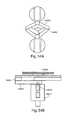
- a semiconductor manufacturing facility described hereinmay include at least one tumble gripper for receiving a semiconductor wafer, the tumble gripper including a pair of gripping modules, wherein each gripping module is configured to receive one of a pair of parallel edges of the semiconductor wafer, wherein each gripping module rotates upon receiving a semiconductor wafer into a position wherein a horizontal portion of the gripping module supports the semiconductor wafer in a horizontal plane and a vertical portion of the gripping module prevents the semiconductor wafer from moving in the horizontal plane.
- a method of handling a semiconductor wafer as described hereinmay include providing an end effector for holding a semiconductor wafer, wherein the end effector includes a receiving slot configured to support the semiconductor wafer on a horizontal plane while preventing the semiconductor wafer from moving in the horizontal plane and wherein the end effector includes a ramp configured to slide the semiconductor wafer into the receiving slot when the semiconductor wafer is placed onto the end effector.
- a semiconductor handling system as described hereinmay include a plurality of robotic arms, at least two of the plurality of robotic arms sharing a common drive facility. At least of the plurality of robotic arms may be a SCARA arm. At least one of the plurality of robotic arms is a four-link SCARA arm. At least two of the plurality of robotic arms may operate independently, or may operate dependently.
- a semiconductor handling system described hereinmay include a robotic arm having a frog-leg arm configuration, the frog-leg arm configuration including at least two pairs of frog leg arms.
- robotshall include any kind of known robot or similar device or facility that includes a mechanical capability and a control capability, which may include a combination of a controller, processor, computer, or similar facility, a set of motors or similar facilities, one or more resolvers, encoders or similar facilities, one or more mechanical or operational facilities, such as arms, wheels, legs, links, claws, extenders, grips, nozzles, sprayers, effectors, actuators, and the like, as well as any combination of any of the above.
- One embodimentis a robotic arm.
- driveshall include any form of drive mechanism or facility for inducing motion. In embodiments it includes the motor/encoder section of a robot.
- axisshall include a motor or drive connected mechanically through linkages, belts or similar facilities, to a mechanical member, such as arm member.
- An “N-axis drive”shall include a drive containing N axes; for example a “2-axis drive” is a drive containing two axes.
- armshall include a passive or active (meaning containing motors/encoders) linkage that may include one or more arm or leg members, bearings, and one or more end effectors for holding or gripping material to be handled.
- SCARA armshall mean a Selectively Compliant Assembly Robot Arm (SCARA) robotic arm in one or more forms known to those of skill in the art, including an arm consisting of one or more upper links connected to a drive, one or more lower links connected through a belt or mechanism to a motor that is part of the drive, and one or more end units, such as an end effector or actuator.
- SCARASelectively Compliant Assembly Robot Arm
- turn radiusshall mean the radius that an arm fits in when it is fully retracted.
- eachshall include, with respect to a robotic arm, the maximum reach that is obtained when an arm is fully extended. Usually the mechanical limit is a little further out than the actual effective reach, because it is easier to control an arm that is not completely fully extended (in embodiments there is a left/right singularity at full extension that can be hard to control).
- “containment”shall mean situations when the arm is optimally retracted such that an imaginary circle can be drawn around the arm/end effector/material that is of minimum radius.
- the “reach-to-containment ratio”shall mean, with respect to a robotic arm, the ratio of maximum reach to minimum containment.
- robot-to-robot distanceshall include the horizontal distance between the mechanical central axis of rotation of two different robot drives.
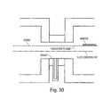
- slot valveshall include a rectangular shaped valve that opens and closes to allow a robot arm to pass through (as opposed to a vacuum (isolation) valve, which controls the pump down of a vacuum chamber).
- SEMI E21.1-1296 standard(a published standard for semiconductor manufacturing) the slot valve for 300 mm wafers in certain semiconductor manufacturing process modules has an opening width of 336 mm, a opening height of 50 mm and a total valve thickness of 60 mm with the standard also specifying the mounting bolts and alignment pins.
- transfer planeshall include the plane (elevation) at which material is passed from a robot chamber to a process module chamber through a slot valve.
- the transfer planeis 14 mm above the slot valve centerline.
- sectionshall include a vacuum chamber that has one or more robotic drives in it. This is the smallest repeatable element in a linear system.
- linkshall include a mechanical member of a robot arm, connected on both ends to another link, an end effector, or the robot drive.
- L 1 ,” “L 2 ”, “L 3 ” or the likeshall include the numbering of the arm links starting from the drive to the end effector.
- end effectorshall include an element at an active end of a robotic arm distal from the robotic drive and proximal to an item on which the robotic arm will act.
- the end effectormay be a hand of the robot that passively or actively holds the material to be transported in a semiconductor process or some other actuator disposed on the end of the robotic arm.
- SCARA armrefers to a robotic arm that includes one or more links and may include an end effector, where the arm, under control, can move linearly, such as to engage an object.
- a SCARA armmay have various numbers of links, such as 3, 4, or more.
- 3-link SCARA armshall include a SCARA robotic arm that has three members: link one (L 1 ), link two (L 2 ) and an end effector.
- a drive for a 3-link SCARA armusually has 3 motors: one connected to L 1 , one to the belt system, which in turn connects to the end effector through pulleys and a Z (lift) motor.
- dual SCARA armshall include a combination of two SCARA arms (such as two 3 or 4-link SCARA arms (typically designated A and B)) optionally connected to a common drive.
- the two SCARA armsare either completely independent or share a common link member L 1 .
- a drive for a dual independent SCARA armusually has either five motors: one connected to L 1 -A, one connected to L 1 -B, one connected to the belt system of arm A, one connected to the belt system of arm B, and a common Z (lift) motor.
- a drive for a dual dependent SCARA armusually has a common share L 1 link for both arms A and B and contains typically four motors: one connected to the common link L 1 , one connected to the belt system for arm A, one connected to the belt system for arm B, and a common Z (lift) motor.
- 4-link SCARA armshall include an arm that has four members: L 1 , L 2 , L 3 and an end effector.
- a drive for a 4-link SCARA armcan have four motors: one connected to L 1 , one to the belt systems connected to L 2 and L 3 , one to the end effector and a Z motor. In embodiments only 3 motors are needed: one connected to L 1 , one connected to the belt system that connects to L 2 , L 3 and the end effector, and a Z motor.
- “Frog-leg style arm”shall include an arm that has five members: L 1 A, L 1 B, L 2 A, L 3 B and an end effector.
- a drive for a frog-leg armcan have three motors, one connected to L 1 A—which is mechanically by means of gearing or the like connected to L 1 B—, one connected to a turret that rotates the entire arm assembly, and a Z motor.
- the drivecontains three motors, one connected to L 1 A, one connected to L 1 B and a Z motor and achieves the desired motion through coordination between the motors.
- Double Frog-leg style armshall include an arm that has eight members L 1 A, L 1 B, L 2 A- 1 , L 2 A- 2 , L 2 B- 1 , L 2 B- 2 and two end effectors.
- the second link members L 2 A- 1 and L 2 B- 1form a single Frog-leg style arm, whereas the second link members L 2 A- 2 and L 2 B- 2 also form a single Frog-leg style arm, however facing in an opposite direction.
- a drive for a dual frog armmay be the same as for a single frog arm.
- Leap Frog-leg style armshall include an arm that has eight members L 1 A, L 1 B, L 2 A- 1 , L 2 A- 2 , L 2 B- 1 , L 2 B- 2 and two end effectors.
- the first link members L 1 A and L 1 Bare each connected to one of the motors substantially by their centers, rather than by their distal ends.
- the second link members L 2 A- 1 and L 2 B- 1form a single Frog-leg style arm, whereas the second link members L 2 A- 2 and L 2 B- 2 also form a single Frog-leg style arm, however facing in the same direction.
- a drive for a dual frog armmay be the same as for a single frog arm.
- FIG. 1shows equipment architectures for a variety of manufacturing equipment types.
- FIG. 2shows a conventional, cluster-type architecture for handling items in a semiconductor manufacturing process.
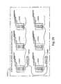
- FIGS. 3A and 3Bshow a series of cluster-type systems for accommodating between two and six process modules.
- FIG. 4shows high-level components of a linear processing architecture for handling items in a manufacturing process.
- FIG. 5shows a top view of a linear processing system, such as one with an architecture similar to that of FIG. 4 .
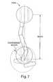
- FIG. 7shows reach and containment characteristics of a SCARA arm.
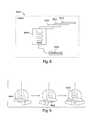
- FIG. 8shows high-level components for a robot system.
- FIG. 9shows components of a dual-arm architecture for a robotic arm system for use in a handling system.
- FIG. 10shows reach and containment capabilities of a 4-link SCARA arm.
- FIGS. 11A and 11Bshow interference characteristics of a 4-link SCARA arm.
- FIG. 12shows a side view of a dual-arm set of 4-link SCARA arms using belts as the transmission mechanism.
- FIGS. 13A , 13 B, and 13 Cshow a side view of a dual-arm set of 4-link SCARA arms using a spline link as the transmission mechanism.
- FIG. 14shows an external return system for a handling system having a linear architecture.
- FIG. 14Ashows a U-shaped configuration for a linear handling system.
- FIG. 15shows certain details of an external return system for a handling system of FIG. 14 .
- FIG. 16shows additional details of an external return system for a handling system of FIG. 14 .
- FIG. 17shows movement of the output carrier in the return system of FIG. 14 .
- FIG. 18shows handling of an empty carrier in the return system of FIG. 14 .
- FIG. 19shows movement of the empty carrier in the return system of FIG. 14 into a load lock position.
- FIG. 20shows the empty carrier lowered and evacuated and movement of the gripper in the return system of FIG. 14 .
- FIG. 21shows an empty carrier receiving material as a full carrier is being emptied in the return system of FIG. 14 .
- FIG. 22shows an empty carrier brought to a holding position, starting a new return cycle in the return system of FIG. 14 .
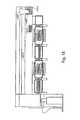
- FIG. 23shows an architecture for a handling facility for a manufacturing process, with a dual-arm robotic arm system and a return system in a linear architecture.
- FIG. 24shows an alternative embodiment of an overall system architecture for a handling method and system of the present invention.
- FIGS. 25A and 25Bshow a comparison of the footprint of a linear system as compared to a conventional cluster system.
- FIG. 26shows a linear architecture deployed with oversized process modules in a handling system in accordance with embodiments of the invention.
- FIG. 27shows a rear-exit architecture for a handling system in accordance with embodiments of the invention.
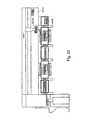
- FIGS. 28A and 28Bshow a variety of layout possibilities for a fabrication facility employing linear handling systems in accordance with various embodiments of the invention.
- FIG. 29shows an embodiment of the invention wherein a robot may include multiple drives and/or multiple controllers.
- FIG. 30shows transfer plane and slot valve characteristics relevant to embodiments of the invention.
- FIG. 31shows a tumble gripper for centering wafers.
- FIG. 32shows a passive sliding ramp for centering wafers.
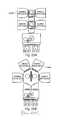
- FIG. 33illustrates a fabrication facility including a mid-entry facility.
- FIGS. 34A , 34 B, and 34 Cillustrate a fabrication facility including a mid-entry facility from a top view.
- FIG. 35illustrates a fabrication facility including the placement of optical sensors for detection of robotic arm position and materials in accordance with embodiments of the invention.
- FIGS. 36A , 36 B, and 36 Cillustrate a fabrication facility in a cross-sectional side view showing optical beam paths and alternatives beam paths.
- FIGS. 37A and 37Billustrate how optical sensors can be used to determine the center of the material handled by a robotic arm.
- FIG. 38shows a conventional 3-axis robotic vacuum drive architecture
- FIG. 39shows a novel 3-axis robotic vacuum drive architecture in accordance with embodiments of the invention.
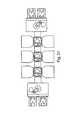
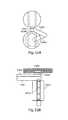
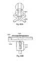
- FIG. 40Aillustrates a vertically arranged load lock assembly in accordance with embodiments of the invention.
- FIG. 40Billustrates a vertically arranged load lock assembly at both sides of a wafer fabrication facility in accordance with embodiments of the invention.
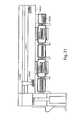
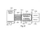
- FIG. 41shows a vertically arranged load lock and vertically stacked process modules in accordance with embodiments of the invention.
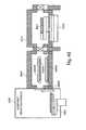
- FIG. 42shows a linearly arranged, two-level handling architecture with vertically stacked process modules in a cross-sectional side view in accordance with embodiments of the invention.
- FIG. 43shows the handling layout of FIG. 42 in a top view.
- FIG. 44shows an instrumented object on a robotic arm with sensors to detect proximity of the object to a target, in accordance with embodiments of the invention.
- FIG. 45illustrates how the movement of sensors over a target can allow the robotic arm to detect its position relative to the obstacle.
- FIG. 46shows how an instrumented object can use radio frequency communications in a vacuum environment to communicate position to a central controller.
- FIG. 47illustrates the output of a series of sensors as a function of position.
- FIG. 48illustrates how heating elements can be placed in a load lock for thermal treatment of objects in accordance with embodiments of the invention.
- FIGS. 49A and 49Bshow an end effector tapered in two dimensions, which reduces active vibration modes in the end effector.
- FIGS. 50A and 50Bshow how vertical tapering of robotic arm elements for a robot planar arm can be used to reduce vibration in the arm set, without significantly affecting vertical stacking height.
- FIGS. 51A and 51Billustrate a dual independent SCARA robotic arm.
- FIGS. 52A and 52Billustrate a dual dependent SCARA robotic arm.
- FIGS. 53A and 53Billustrate a frog-leg style robotic arm.
- FIGS. 54A and 54Billustrate a dual frog-leg style robotic arm.
- FIG. 55Aillustrates a 4-Link SCARA arm mounted on a moveable cart, as well as a 4-Link SCARA arm mounted on an inverted moveable cart.
- FIG. 55Billustrates a top view of FIG. 55A .
- FIG. 56illustrates using a 3-link single or dual SCARA arm robotic system to pass wafers along a substantially a linear axis.
- FIG. 57illustrates a 2-level vacuum handling robotic system where the top and bottom process modules are accessible by means of a vertical axis in the robotic arms.
- FIG. 58Ashows a two level processing facility where substrates are passed along a substantially linear axis on one of the two levels.
- FIG. 58Billustrates a variation of FIG. 58A where substrates are removed from the rear of the system.
- FIG. 59Ashows a manufacturing facility which accommodates very large processing modules in a substantially linear axis. Service space is made available to allow for access to the interior of the process modules.
- FIG. 59Billustrates a more compact layout for 4 large process modules and one small process module.
- FIGS. 60A and 60Billustrate a dual frog-leg style robotic manipulator with substrates on the same side of the system.
- FIG. 1shows equipment architectures 1000 for a variety of manufacturing equipment types.
- Each type of manufacturing equipmenthandles items, such as semiconductor wafers, between various processes, such as chemical vapor deposition processes, etching processes, and the like.
- semiconductor manufacturing processesare typically extremely sensitive to contaminants, such as particulates and volatile organic compounds, the processes typically take place in a vacuum environment, in one or more process modules that are devoted to specific processes.
- Semiconductor wafersare moved by a handling system among the various processes to produce the end product, such as a chip.
- Various configurations 1000exist for handling systems.
- a prevalent systemis a cluster tool 1002 , where process modules are positioned radially around a central handling system, such as a robotic arm.
- a handling systemcan rotate items horizontally, such as in the embodiment 1004 .
- An important aspect of each type of toolis the “footprint,” or the area that the equipment takes up in the semiconductor manufacturing facility. The larger the footprint, the more space required to accommodate multiple machines in a fabrication facility. Also, larger footprints typically are associated with a need for larger vacuum systems, which increase greatly in cost as they increase in size.
- the architecture 1004rotates items in a “lazy Susan” facility.
- the architecture in 1006moves items in and out of a process module where the process modules are arranged next to each other.
- the architecture 1008positions process modules in a cluster similar to 1002 , with the difference that the central robot handles two wafers side by side.
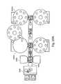
- FIG. 2shows a conventional cluster-type architecture 2000 for handling items in a semiconductor manufacturing process.
- a robotic arm 2004moves items, such as wafers, among various process modules 2002 that are positioned in a cluster around the robotic arm 2004 .
- An atmospheric substrate handling mini-environment chamber 2008receives materials for handling by the equipment and holds materials once processing is complete. Note how difficult it would be to add more process modules 2002 . While one more module 2002 would potentially fit, the practical configuration is limited to five process modules 2002 . Adding a sixth module may significantly impact the serviceability of the equipment, in particular the robotic arm 2004 .
- FIGS. 3A and 3Bshow cluster tool modules, atmospheric mini-environment handling chambers, vacuum handling chambers and other components 3000 from a flexible architecture system for a vacuum based manufacturing process.
- Different modulescan be assembled together to facilitate manufacturing of a desired process technology.
- a given chipmay require chemical vapor deposition of different chemical constituents (e.g., Titanium Nitride, Tungsten, etc.) in different process modules, as well as etching in other process modules.
- the sequence of the processes in the different process modulesproduces a unique end product.
- cluster toolscan include configurations with two 3002 , three 3004 , four 3006 , five 3008 , 3010 or six 3012 process modules with staged vacuum isolation. Other components can be supplied in connection with the equipment.
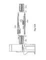
- FIG. 4shows high-level components of a linear processing architecture 4000 for handling items in a manufacturing process.
- the architectureuses two or more stationary robots 4002 arranged in a linear fashion.
- the robots 4002can be either mounted in the bottom of the system or hang down from the chamber lid or both at the same time.
- the linear systemuses a vacuum chamber 4012 around the robot.
- the systemcould be comprised of multiple connected vacuum chambers 4012 , each with a vacuum chamber 4012 containing its own robot arranged in a linear fashion.
- a single controllercould be set up to handle one or more sections of the architecture.
- vacuum chambers 4012 sectionsare extensible; that is, a manufacturer can easily add additional sections/chambers 4012 and thus add process capacity, much more easily than with cluster architectures.
- each sectionuses independent robot drives 4004 and arms 2004 , the throughput may stay high when additional sections and thus robots are added.
- cluster toolswhen the manufacturer adds process chambers 2002 , the system increases the load for the single robot, even if that robot is equipped with a dual arm, eventually the speed of the robot can become the limiting factor.
- systemsaddress this problem by adding additional robot arms 2004 into a single drive.
- Other manufacturershave used a 4-axis robot with two completely independent arms such as a dual SCARA or dual Frog-leg robots.
- the linear system disclosed hereinmay not be limited by robot capacity, since each section 4012 contains a robot, so each section 4012 is able to transport a much larger volume of material than with cluster tools.
- the components of the systemcan be controlled by a software controller, which in embodiments may be a central controller that controls each of the components.
- the componentsform a linkable handling system under control of the software, where the software controls each robot to hand off a material to another robot, or into a buffer for picking up by the next robot.
- the software control systemmay recognize the addition of a new component, such as a process module or robot, when that component is plugged into the system, such as recognizing the component over a network, such as a USB, Ethernet, FireWire, Bluetooth, 802.11a, 802.11a, 802.11g or other network.
- a software schedulerfor the flow of a material to be handled, such as a wafer, can be reconfigured automatically so that the materials can be routed over the new link in the system.
- the software scheduleris based on a neural net, or it can be a rule-based scheduler.
- process modulescan make themselves known over such a network, so that the software controller knows what new process modules, robots, or other components have been connected. When a new process module is plugged into an empty facet, the system can recognize it and allow it to be scheduled into the flow of material handling.
- the software systemmay include an interface that permits the user to run a simulation of the system.
- the interfacemay allow a user to view the linking and configuration of various links, robotic arms and other components, to optimize configuration (such as by moving the flow of materials through various components, moving process modules, moving robots, or the like), and to determine what configuration to purchase from a supplier.
- the interfacemay be a web interface.
- the methods and system disclosed hereincan use optional buffer stations 4010 between robot drives. Robots could hand off to each other directly, but that is technically more difficult to optimize, and would occupy two robots, because they would both have to be available at the same time to do a handoff, which is more restrictive than if they can deposit to a dummy location 4010 in-between them where the other robot can pick up when it is ready.
- the buffer 4010also allows higher throughput, because the system does not have to wait for both robots to become available.
- the buffers 4010may also offer a good opportunity to perform some small processing steps on the wafer such as heating, cooling, aligning, inspection, metrology, testing or cleaning.
- the methods and systems disclosed hereinuse optional vacuum isolation valves 4006 between robot areas/segments 4012 .
- Each segment 4012can be fully isolated from any other segment 4012 . If a robot handles ultra clean and sensitive materials (e.g., wafers) in its segment 4012 , then isolating that segment 4012 from the rest of the system may prevent cross-contamination from the dirtier segment 4012 to the clean segment 4012 .
- the manufacturercan now operate segments 4012 at different pressures. The manufacturer can have stepped vacuum levels where the vacuum gets better and better further into the machine.
- the big advantage of using vacuum isolation valves 4006 between segments 4012may be that handling of atomically clean wafers (created after cleaning steps and needing to be transported between process modules without contamination from the environment) can be done without out-gassing from materials or wafers in other parts of the system entering the isolated chamber segment 4012 .
- vacuum isolation between robotsis possible, as is material buffering between robots, such as using a buffer module 4010 , a mini-process module or an inspection module 4010 .
- FIG. 5shows a top view of a linear processing system 4000 , such as one with a linear architecture similar to that of FIG. 4 .
- robotscan be used in semiconductor manufacturing equipment, whether a cluster tool or a linear processing machine such as disclosed in connection with FIGS. 4 and 5 .
- FIG. 6shows a 3-link SCARA arm 6002 and a 4-link SCARA arm 6004 .
- the 3-link or 4-link arms 6002 , 6004are driven by a robot drive.
- the 3-link arm 6002is commonly used in industry.
- the systemis not optimized in that the reach-to-containment ratio is not very good.
- the vacuum chambersneed to be bigger, and since costs rise dramatically with the size of the vacuum chamber, having a 3-link SCARA arm 6002 can increase the cost of the system.
- the overall footprint of the systembecomes bigger with the 3-link SCARA arm 6002 .
- the reach of a 3-link SCARA arm 6002is less than that of a 4-link arm 6004 .
- a manufacturermay wish to achieve a large, deep handoff into a process module, and the 4-link arm 6004 reaches much farther beyond its containment ratio. This has advantages in some non-SEMI-standard process modules. It also has advantages when a manufacturer wants to cover large distances between segments.
- the 4-link arm 6004is advantageous in that it folds in a much smaller containment ratio than a 3-link SCARA arm 6002 , but it reaches a lot further than a conventional 3-link SCARA 6002 for the same containment diameter. In combination with the ability to have a second drive and second 4-link arm 6004 mounted on the top of the system, it may allow for a fast material swap in the process module.
- the 4-link SCARA arm 6004may be mounted, for example, on top of a stationary drive as illustrated, or on top of a moving cart that provides the transmission of the rotary motion to actuate the arms and belts. In either case, the 4-link arm 6004 , optionally together with a second 4-link arm 6004 , may provide a compact, long-reach arm that can go through a small opening, without colliding with the edges of the opening.
- FIG. 7shows reach and containment characteristics of a 4-link SCARA arm 7004 .
- the 4-link SCARA arm 7004 link lengthsare not constrained by the optimization of reach to containment ratio as in some other systems. Optimization of the reach to containment ratio may lead to a second arm member that is too long. When the arm reaches through a slot valve that is placed as close as practical to the minimum containment diameter, this second arm member may collide with the inside edges of the slot valve.
- the second (and third) linksmay be dimensioned based on collision avoidance with a slot valve that the arm is designed to reach through. This results in very different ratios between links one, two, and three.
- the length of link twomay constrain the length of link three.
- An equation for optimum arm lengthmay be a 4th power equation amenable to iterative solutions.
- FIG. 8shows high-level components for a robot system 8002 , including a controller 8004 , a drive/motor 8008 , an arm 8010 , an end effector 8012 , and a material to be handled 8014 .
- FIG. 9shows components of a dual-arm 9002 architecture for a robotic arm system for use in a handling system.
- One armis mounted from the bottom 9004 and the other from the top 9008 .
- bothare 4-link SCARA arms.
- Mounting the second arm on the topis advantageous.
- the lower and upper drivesare conventionally mechanically coupled.
- the second (top) arm 9008may optionally be included only if necessary for throughput reasons.
- Another featureis that only two motors, just like a conventional SCARA arm, may be needed to drive the 4-link arm. Belts in the arm may maintain parallelism. Parallelism or other coordinated movements may also be achieved, for example, using parallel bars instead of belts.
- the use of only two motorsmay provide a substantial cost advantage.
- three motorsmay provide a functional advantage in that the last (L 4 ) link may be independently steered, however the additional belts, bearings, connections, shafts and motor may render the system much more expensive.
- the extra beltsmay add significant thickness to the arm mechanism, making it difficult to pass the arm through a (SEMI standard) slot valve.
- the use of fewer motorsgenerally simplifies related control software.
- the wristmay be offset from centerline. Since the ideal system has a top-mount 9008 as well as a bottom 9004 mount 4-link arm, the vertical arrangement of the arm members may be difficult to adhere to if the manufacturer also must comply with the SEMI standards. In a nutshell, these standards specify the size and reach requirements through a slot valve 4006 into a process module. They also specify the level above centerline on which a wafer has to be carried. Many existing process modules are compliant with this standard. In systems that are non-compliant, the slot valves 4006 are of very similar shape although the opening size might be slightly different as well as the definition of the transfer plane. The SEMI standard dimensional restrictions require a very compact packaging of the arms.
- top 9008 and bottom 9004 armscan get closer together, making it easier for them to pass through the slot valve 4006 . If the wrist is not offset, then the arms need to stay further apart vertically and wafer exchanges may take more time, because the drives need to move more in the vertical direction.
- the proposed design of the top armdoes not require that there is a wrist offset, but a wrist offset may advantageously reduce the turn radius of the system, and allows for a better mechanical arm layout, so no interferences occur.
- FIG. 10shows reach and containment capabilities of a 4-link SCARA arm 6004 .
- FIG. 11shows interference characteristics 1102 of a 4-link SCARA arm 6004 .
- the wrist offsetmay help to fold the arm in a smaller space than would otherwise be possible.
- FIG. 12shows a side view of a dual-arm set of 4-link SCARA arms 6004 . Because of the packaging constraints of particularly the top arm, it may be necessary to construct an arm that has some unique features. In embodiments, one link upon retracting partially enters a cutout in another arm link. Belts can be set in duplicate, rather than a single belt, so that one belt is above 12004 and one below 12008 the cutout.
- One solution, which is independent of the fact that this is a 4-link arm,is to make link two 6004 significantly lower 12002 , with a vertical gap relative to the first link, so that third and fourth link can fold inside. Lowering the second link 12002 may allow the third and fourth link to reach the correct transfer plane and may allow a better containment ratio. Because of the transfer plane definition, the lowering of the second link 12002 may be required.
- FIG. 13shows an embodiment in which a combination of belts and linkages is used.
- the transmission of motion through a first link 13002 and a third link 13006may be accomplished by either a single belt or a dual belt arrangement for the positioning of the end effector 13008 .
- the motion transmission in a second link 13004may be accomplished by a mechanical linkage (spline) 13010 .
- the advantage of such an arrangementmay be that enclosed joints can be used which reduces the vertical dimension of the arm assembly that may allow an arm to more easily pass through a SEMI standard slot valve.
- FIG. 14shows an external return system for a handling system having a linear architecture 14000 .
- the return mechanismis optionally on the top of the linear vacuum chamber.
- the return pathis often through the same area as the entry path. This opens up the possibility of cross contamination, which occurs when clean wafers that are moving between process steps get contaminated by residuals entering the system from dirty wafers that are not yet cleaned. It also makes it necessary for the robot 4002 to handle materials going in as well as materials going out, and it makes it harder to control the vacuum environment.
- the air returnmay relatively cheap to implement; the air return may free up the vacuum robots 4002 because they do not have to handle materials going out; and the air return may keep clean finished materials out of the incoming areas, thereby lowering cross-contamination risks.
- Employing a small load lock 14010 in the rearmay add some costs, and so may the air tunnel 14012 , so in systems that are short and where vacuum levels and cross contamination are not so important, an air return may have less value, but in long systems with many integrated process steps the above-system air return could have significant benefits.
- the return systemcould also be a vacuum return, but that would be more expensive and more complicated to implement.
- a load lock 14010may be positioned at the end of a linear system, as depicted in FIG. 14 , the load lock 14010 could be positioned elsewhere, such as in the middle of the system.
- a manufacturing itemcould enter or exit the system at such another point in the system, such as to exit the system into the air return.
- the advantage of a mid-system exit pointmay be that in case of a partial system failure, materials or wafers can be recovered.
- the advantage of a mid-system entry pointmay be that wafers can be inserted in multiple places in the system, allowing for a significantly more flexible process flow.
- FIG. 14Ashows an example of a U-shaped linear system.
- an embodiment of the systemuses a dual carrier mechanism 14008 so that wafers that are finished can quickly be returned to the front of the system, but also so that an empty carrier 14008 can be placed where a full one was just removed.
- the air returnwill feature a carrier 14008 containing N wafers. N can be optimized depending on the throughput and cost requirements.
- the air return mechanismmay contain empty carriers 14008 so that when a full carrier 14018 is removed from the vacuum load lock 14010 , a new empty carrier 14008 can immediately be placed and load lock 14010 can evacuated to receive more materials.
- the air return mechanismmay be able to move wafers to the front of the system.
- a vertical lift 14004may be employed to lower the carrier to a level where the EFEM (Equipment Front End Module) robot can reach.
- the vertical lift 14004can lower to pick an empty carrier 14008 from the load lock.
- the air return mechanismmay feature a storage area 14014 for empty carriers 14008 , probably located at the very end and behind the location of the load lock 14010 .
- the reason for thisis that when the load lock 14010 releases a carrier 14018 , the gripper 14004 can grip the carrier 14018 and move it forward slightly. The gripper 14004 can then release the full carrier 14018 , move all the way back and retrieve an empty carrier 14008 , place it on the load lock 14010 . At this point the load lock 14010 can evacuate. The gripper 14004 can now go back to the full carrier 14018 and move it all the way to the front of the system. Once the carrier 14018 has been emptied by the EFEM, it can be returned to the very back where it waits for the next cycle.
- FIG. 15shows certain additional details of an external return system for a handling system of FIG. 14 .
- FIG. 16shows additional details of an external return system for a handling system of FIG. 14 .
- FIG. 17shows movement of the output carrier 14018 in the return tunnel 14012 of FIG. 14 .
- the gripper 14004is shown in a position 17002 within the return tunnel 14012 away from the load lock 14010 . Once in the return tunnel 14012 the gripper 14004 may move to any available position 17012 within the return tunnel 14012 .
- FIG. 18shows handling of an empty carrier 14008 in the return system 14012 of FIG. 14 .
- FIG. 19shows movement of the empty carrier 14008 in the return tunnel 14012 of FIG. 14 into a load lock 14010 position.
- FIG. 20shows the empty carrier 14008 lowered and evacuated and movement of the gripper 14004 in the return system of FIG. 14 .
- FIG. 21shows an empty carrier 14008 receiving material as a full carrier 14018 is being emptied in the return tunnel 14012 of FIG. 14 .
- FIG. 22shows an empty carrier 14008 brought to a holding position, starting a new return cycle in the return tunnel 14012 of FIG. 14 .
- FIG. 23shows an architecture for a handling facility for a manufacturing process, with a dual-arm robotic arm system 23002 and a return system in a linear architecture.
- FIG. 24shows an alternative embodiment of an overall system architecture for a handling method and system of the present invention.
- FIG. 25shows a comparison of the footprint of a linear system 25002 as compared to a conventional cluster system 25004 .
- the manufacturercan easily extend the machine with additional modules without affecting system throughput.
- FIG. 26shows a linear architecture deployed with oversized process modules 26002 in a handling system in accordance with embodiments of the invention.
- FIG. 27shows a rear-exit architecture for a handling system in accordance with embodiments of the invention.
- FIG. 28shows a variety of layout possibilities for a fabrication facility employing linear handling systems in accordance with various embodiments of the invention.
- FIG. 29shows an embodiment of the invention wherein a robot 29002 may include multiple drives 29004 and/or multiple controllers 29008 .
- a controller 29008may control multiple drives 29004 as well as other peripheral devices such as slot valves, vacuum gauges, thus a robot 29002 may be a controller 29008 with multiple drives 29004 or multiple controllers 29008 with multiple drives 29004 .
- FIG. 30shows transfer plane 30002 and slot valve 30004 characteristics relevant to embodiments of the invention.
- FIG. 31shows a tumble gripper 31002 for centering wafers.
- the advantage of the tumble gripper 31002 over the passive centering gripper 32002 in FIG. 32is that there is less relative motion between the tumblers 31004 and the backside of the wafer 31008 .
- the tumblers 31004may gently nudge the wafer 31008 to be centered on the end effector, supporting it on both sides as it moves down. In certain manufacturing processes it may be desirable to center wafers 31008 , such as in a vacuum environment.
- the tumble gripper 31004may allow the handling of very fragile wafers 31008 , such as when employing an end effector at the end of a robotic arm, because it supports both ends of the wafer during handling.
- FIG. 32shows a passively centering end effector 32002 for holding wafers 31008 .
- the wafer 31008is typically slightly off-center when the end effector lifts (or the wafer 31008 is lowered). This results in the wafer 31008 sliding down the ramp and dropping into the cutout 32004 . This can result in the wafer 31008 abruptly falling or moving, which in turn can create particles.
- the methods and systems disclosed hereinoffer many advantages in the handling of materials or items during manufacturing processes. Among other things, vacuum isolation between robots may be possible, as well as material buffering between robots. A manufacturer can return finished wafers over the top of the system without going through vacuum, which can be a very substantial advantage, requiring only half the necessary handling steps, eliminating cross contamination between finished and unfinished materials and remaining compatible with existing clean room designs. When a manufacturer has relatively dirty wafers entering the system, the manufacturer may want to isolate them from the rest of the machine while they are being cleaned, which is usually the first step in the process. It may be advantageous to keep finished or partially finished materials away from the cleaning portion of the machine.
- the dual armsmay work in coordinated fashion, allowing very fast material exchanges. Regardless of the exact arm design (3-link, 4-link or other), mounting an arm in the lid that is not mechanically connected to the arm in the bottom can be advantageous.
- the link lengths of the 4-link SCARA arm provided hereincan be quite advantageous, as unlike conventional arms they are determined by the mechanical limits of slot valves and chamber radius.
- the 4-link SCARA arms disclosed hereinare also advantageous in that they can use two motors for the links, along with a Z motor, rather than three motors plus the Z motor.
- a linear vacuum system where materials exit in the rearmay offer substantial benefits.
- Another implementationmay be to have both the entry system and exit system installed through two opposing walls.
- the 4-link SCARA arm disclosed hereinmay also allow link L 3 to swing into and over link L 2 for the top robot drive. This may not be easily done with the 3-link SCARA, nor with existing versions of 4-link SCARA arms, because they have the wrong link lengths.
- the gripper for carriers and the multiple carrier locations in the linear systemmay also offer substantial benefits in materials handling in a linear manufacturing architecture. Including vertical movement in the gripper and/or in the rear load lock may offer benefits as well.
- FIG. 33illustrates a fabrication facility including a mid-entry point 33022 .
- the fabrication facilitymay include a load lock 14010 mid-stream 33002 where wafers 31008 can be taken out or entered.
- the air return system 14012can also take new wafers 31008 to the midpoint 33022 and enter wafers 31008 there.
- FIG. 34illustrates several top views of a fabrication facility with mid-entry points 33002 . The figure also illustrates how the combination of a mid-entry point effectively functions to eliminate one of the EFEMs 34002 .
- FIG. 35illustrates a fabrication facility including a series of sensors 35002 .
- sensors 35002are commonly used to detect whether a material 35014 is still present on a robotic arm 35018 .
- Such sensors 35002may be commonly placed at each vacuum chamber 4012 entry and exit point.
- Such sensors 35002may consist of a vertical optical beam, either employing an emitter and detector, or employing a combination emitter/detector and a reflector.
- the training of robotic stationsis commonly accomplished by a skilled operator who views the position of the robot arm and materials and adjusts the robot position to ensure that the material 35014 is deposited in the correct location.
- frequently these positionsare very difficult to observe, and parallax and other optical problems present significant obstacles in properly training a robotic system.
- a training procedurecan consume many hours of equipment downtime.
- a series of sensors 35002 - 35010may include horizontal sensors 35004 - 35010 and vertical sensors 35002 .
- This combination of sensors 35002 - 35010may allow detection, for example through optical beam breaking, of either a robotic end effector, arm, or a handled object.
- the vertical sensor 35002may be placed slightly outside the area of the wafer 31008 when the robotic arm 35018 is in a retracted position.
- the vertical sensor 35002may also, or instead, be placed in a location such as a point 35012 within the wafer that is centered in front of the entrance opening and covered by the wafer when the robot is fully retracted. In this position the sensor may be able to tell the robotic controller that it has successfully picked up a wafer 31008 from a peripheral module.
- Horizontal sensors 35004 - 35010may also be advantageously employed.
- horizontal sensors 35004 - 35010are sometimes impractical due to the large diameter of the vacuum chamber, which may make alignment of the horizontal sensors 35004 - 35010 more complicated.
- the chamber sizemay be reduced significantly, thus may make it practical to include one or more horizontal sensors 35004 - 35010 .
- FIG. 36illustrates other possible locations of the horizontal sensors 35004 - 35010 and vertical sensors 35002 , such as straight across the chamber ( 36002 and 36008 ) and/or through mirrors 36006 placed inside the vacuum system to detect that material 35014 is present.
- FIG. 37illustrates a possible advantage of placing the sensor 35002 slightly outside the wafer 37001 radius when the robot arm is fully retracted.
- the sensor 35002detects the leading edge of the wafer 37001 at point “a” 37002 and the trailing edge at point “b” 37004 .
- These resultsmay indicate that the wafer 37001 was successfully retrieved, but by tying the sensor 35002 signal to the encoders, resolvers or other position elements present in the robotic drive, one can also calculate if the wafer 37001 is centered with respect to the end effector.
- the midpoint of the line segment “a-b” 37002 37004should correspond to the center of the end effector because of the circular geometry of a wafer 37001 . If the wafer 37001 slips on the end effector, inconsistent length measurements may reveal the slippage.
- a second line segment “c-d” 37008 37010may be detected when the wafer 37001 edges pass through the sensor. Again, the midpoint between “c” 37008 and “d” 37010 should coincide with the center of the end effector, and may permit a measurement or confirmation of wafer centering.
- the above methodmay allow the robot to detect the wafer 37001 as well as determine if the wafer 37001 is offset from the expected location on the end effector.
- the combination of horizontal and vertical sensors 35002 - 35010may allow the system to be taught very rapidly using non-contact methods: the robotic arm and end effectors may be detected optically without the need for mechanical contact. Furthermore, the optical beams can be used during real-time wafer 37001 handling to verify that wafers 37001 are in the correct position during every wafer 37001 handling move.
- FIG. 38illustrates a conventional vacuum drive 38000 with two rotary axes 38020 and 38018 and a vertical (Z) axis 38004 .
- a bellows 38016may allow for the vertical Z-axis 38002 motion.
- a thin metal cylinder 38024 affixed to the bottom of the bellows 18016may provide a vacuum barrier between the rotor and the stator of the motors 38010 and 38014 . This arrangement may require in-vacuum placement of many components: electrical wires and feedthroughs, encoders, signal LEDs and pick-ups 38008 , bearings 38012 , and magnets 38006 .
- Magnets 38006 , bearings 38012 , wires and connectors, and encoderscan be susceptible to residual processing gasses present in the vacuum environment. Furthermore, it may be difficult to remove gasses trapped in the bottom of the cylinder 38024 , as the gasses may have to follow a convoluted path 38022 when evacuated.
- FIG. 39illustrates a vacuum robot drive 39000 that may be used with the systems described herein.
- the rotary drive forcesmay be provided by two motor cartridges 39004 and 39006 .
- Each cartridgemay have an integral encoder 39008 , bearings 39018 and magnets 39020 . Some or all of these components may be positioned outside the vacuum envelope.
- a concentric dual-shaft rotary seal unit 39016may provide vacuum isolation for the rotary motion using, for example, lip-seals or ferrofluidic seals. This approach may reduce the number of components inside the vacuum system. It may also permit servicing of the motors 39004 , 39006 and encoders 39008 without breaking vacuum, thereby increasing serviceability of the drive unit.
- FIG. 40shows a stacked vacuum load lock 4008 , 40004 for entering materials into a vacuum environment.
- One limiting factor on bringing wafers 31008 into a vacuum systemis the speed with which the load lock can be evacuated to high vacuum. If the load lock is pumped too fast, condensation may occur in the air in the load lock chamber, resulting in precipitation of nuclei on the wafer 31008 surfaces, which can result in particles and can cause defects or poor device performance.
- Cluster toolsmay employ two load locks side by side, each of which is alternately evacuated. The pumping speed of each load lock can thus be slower, resulting in improved performance of the system. With two load locks 4008 40004 in a vertical stack, the equipment footprint stays very small, but retains the benefit of slower pumping speed.
- the load lock 40004can be added as an option.
- the robotic arms 4004 and 40006can each access either one of the two load locks 4008 40004 .
- the remaining handoff module 7008could be a single level handoff module.
- FIG. 40Bshows another load lock layout.
- wafers 31008can be entered and can exit at two levels on either side of the system, but follow a shared level in the rest of the system.
- FIG. 41details how the previous concept of stacked load locks 4008 40004 can be also implemented throughout a process by stacking two process modules 41006 , 41008 . Although such modules would not be compliant with the SEMI standard, such an architecture may offer significant benefits in equipment footprint and throughput.
- FIG. 42shows a system with two handling levels 4008 , 40004 , 4010 , 42004 : wafers may be independently transported between modules using either the top link 40006 or the bottom link 4004 .
- each handling levelmay have two load locks to provide the advantage of reduced evacuation speed noted above.
- a system with four input load locks, two handling levels, and optionally four output load locks,is also contemplated by description provided herein, as are systems with additional load lock and handling levels.
- FIG. 43shows a top view of the system of FIG. 42 .
- FIG. 44depicts a special instrumented object 44014 , such as a wafer.
- One or more sensors 44010may be integrated into the object 44014 , and may be able to detect environmental factors around the object 44014 .
- the sensors 44010may include proximity sensors such as capacitive, optical or magnetic proximity sensors.
- the sensors 44010may be connected to an amplifier/transmitter 44012 , which may use battery power to transmit radio frequency or other sensor signals, such as signals conforming to the 802.11b standard, to a receiver 44004 .
- the object 44014can be equipped with numerous sensors of different types and in different geometrically advantageous patterns.
- the sensors 1 through 6( 44010 ) are laid out in a radius equal to the radius of the target object 44008 .
- these sensorsare proximity sensors.
- By comparing the transient signals from the sensors 44010for example sensor 1 and sensor 6 , it can be determined if the object 44014 is approaching a target 44008 at the correct orientation. If the target 44008 is not approached correctly, one of the two sensors 44010 may show a premature trigger.
- the systemmay determine if the object 44010 is properly centered above the target 44008 before affecting a handoff.
- the sensors 44010can be arranged in any pattern according to, for example, efficiency of signal analysis or any other constraints. Radio frequency signals also advantageously operate in a vacuum environment.
- FIG. 45shows the system of FIG. 44 in a side orientation illustrating the non-contact nature of orienting the instrumented object 44014 to a target 44008 .
- the sensors 44010may include other sensors for measuring properties of the target 44008 , such as temperature.
- FIG. 46depicts radio frequency communication with one or more sensors.
- a radio frequency sensor signal 44016may be transmitted to an antenna 46002 within a vacuum. Appropriate selection of wavelengths may improve signal propagation with a fully metallic vacuum enclosure.
- the use of sensors in wireless communication with an external receiver and controllermay provide significant advantages. For example, this technique may reduce the time required for operations such as finding the center of a target, and information from the sensor(s) may be employed to provide visual feedback to an operator, or to automate certain operations using a robotic arm.
- the use of one or more sensorsmay permit measurements within the chamber that would otherwise require release of the vacuum to open and physically inspect the chamber. This may avoid costly or time consuming steps in conditioning the interior of the chamber, such as depressurization and baking (to drive out moisture or water vapor).
- FIG. 47illustrates the output from multiple sensors 44010 as a function of the robot movement.
- the motionmay result in the sensors providing information about, for example, distance to the target 44008 if the sensors are proximity sensors.
- the signalscan be individually or collectively analyzed to determine a location for the target 44008 relative to the sensors. Location or shape may be resolved in difference directions by moving the sensor(s) in two different directions and monitoring sensor signals, without physically contacting the target 44008 .
- FIG. 48depicts a technique for inserting and removing wafers 48008 from a vacuum system.
- One or more heating elementssuch as a set of heating elements 48002 , 48004 , and 48006 may be employed, individually or in combination, to heat a chamber 4008 and a substrate material 48008 to an elevated temperature of 50° C. to 400° C. or more. This increase in starting temperature may mitigate condensation that would otherwise occur as pressure decreases in the chamber, and may allow for a more rapid pump down sequence to create a vacuum.
- heated wafers 48008When heated wafers 48008 are moved to the load lock 4008 by the robotic arm 2004 , they may be significantly warmer than the heating units 48004 , 48006 (formed as “shelves”), such that heating units 48004 , 48006 may cool the wafers on contact.
- a heating power supplymay regulate heat provided to the heating units 48004 48006 to maintain a desired temperature for the heating units and/or wafers.
- a suitable material selection for the heating units 48004 , 48006may result in the system reacting quickly to heating power changes, resulting in the possibility of different temperature settings for different conditions, for example a higher temperature setting during pump-down of the chamber 4008 and a lower setting during venting of chamber 4008 .
- Preheating the wafers 48008may reduce condensation and particles while reducing process time. At the same time, the wafers 48008 may be too hot when exiting the system, such that they present a safety hazard, or melt handling and support materials such as plastic. Internal temperatures of about 80 to 100° C. degrees, and external temperatures of about 50° C. degrees or less may, for example, meet these general concerns.
- FIG. 49illustrates a robotic end effector 49002 .
- the robotic end effector 49002may be tapered so that it has a non-uniform thickness through one or more axes.
- the robotic end effector 49002may have a taper when viewed from the side or from the top.
- the tapermay mitigate resonant vibrations along the effector 49002 .
- a relatively narrow cross-sectional profilewhen viewed from the side) may permit easier maneuvering between wafers 49006 .
- the side-view tapermay be achieved by grinding or machining, or by a casting process of the effector 49002 with a taper.
- AlSiC 9Aluminum Silicon Carbide
- a casting processoffers the additional advantage that the wafer support materials 49004 can be cast into the mold during the casting process, thereby reducing the number of components that require physical assembly.
- FIG. 51shows a dual independent SCARA arm employing five motors 51014 .
- Each lower arm 51002 and 51008can be independently actuated by the motors 51014 .
- the armsare connected at the distal end to upper arms 51004 and 51010 .
- the configurationgives a relatively small retract radius, but a somewhat limited extension.
- FIG. 52shows a dual dependent SCARA arm employing 4 motors 52010 .
- the links 52002 and 52004may be common to the end effectors 52006 and 52008 .
- the motors 52010may control the end effectors 52006 and 52008 in such a way that during an extension motion of the lower arm 52002 , the desired end effector, (say 52008 ) may be extended into the processing modules, whereas the inactive end effector (say 52006 ) may be pointed away from the processing module.
- FIG. 53shows a frog-leg style robotic arm.
- the armcan be used in connection with various embodiments described herein, such as to enable passing of workpieces, such as semiconductor wafers, from arm-to-arm in a series of such arms, such as to move workpieces among semiconductor process modules.
- FIG. 54shows a dual frog-leg arm that can be employed in a planar robotic system, such as one of the linear, arm-to-arm systems described in this disclosure.
- FIG. 55Aillustrates a 4-Link SCARA arm as described in this disclosure mounted to a cart 55004 .
- a cartmay move in a linear fashion by a guide rail or magnetic levitation track 55008 and driven by a motor 55002 internal or external to the system.
- the 4-Link SCARA armhas the advantage that it fold into a smaller retract radius than a 3-Link SCARA arm, while achieving a larger extension into a peripheral module such as a process module all the while avoiding a collision with the opening that the arm has to reach through.
- An inverted cart 55006could be used to pass substrates over the cart 55004 .
- FIG. 55Bshows a top view of the system described in FIG. 55A .
- FIG. 56illustrates a linear system described in this disclosure using a combination of dual independent and single SCARA robotic arms. Such a system may not be as compact as a system employing a 4-Link SCARA arm robotic system.
- FIG. 57demonstrates a vertically stacked handling system employing a 4-Link SCARA robotic arm, where the arm can reach any and all of the peripheral process modules 5002 .
- the armcan reach any and all of the peripheral process modules 5002 .
- the top and bottom of each of the process modulesmay remain exposed for service access as well as for mounting components such as pumps, electrodes, gas lines and the like.
- the proposed layoutmay allow for the combination of seven process modules 5002 in a very compact space.
- FIG. 58Aillustrates a variation of FIG. 57 , where the bottom level 58002 of the system consists of a plurality of robotic systems as described in this disclosure and the top level system 58004 employs process modules 5002 oriented at a 45 degree angle to the main system axis.
- the proposed layoutallows for the combination of nine process modules 5002 in a very compact space.
- FIG. 58Billustrates a variation of FIG. 58A with the use of a rear-exit load lock facility to remove substrates such as semiconductor wafers from the system.
- FIG. 59Ashows a linear handling system accommodating large substrate processing modules 59004 while still allowing for service access 59002 , and simultaneously still providing locations for two standard sized process module 5002 .
- FIG. 59Bdemonstrates a system layout accommodating four large process modules 59004 and a standard sized process module 5002 while still allowing service access 59002 to the interior of process modules 5002 .
- FIG. 60shows a dual frog robot with arms substantially on the same side of the robotic drive component.
- the lower arms 60002support two sets of upper arms 60004 which are mechanically coupled to the motor set 54010 .
Landscapes
- Engineering & Computer Science (AREA)
- Physics & Mathematics (AREA)
- Condensed Matter Physics & Semiconductors (AREA)
- General Physics & Mathematics (AREA)
- Manufacturing & Machinery (AREA)
- Computer Hardware Design (AREA)
- Microelectronics & Electronic Packaging (AREA)
- Power Engineering (AREA)
- Robotics (AREA)
- Container, Conveyance, Adherence, Positioning, Of Wafer (AREA)
Abstract
Description
Claims (20)
Priority Applications (1)
| Application Number | Priority Date | Filing Date | Title |
|---|---|---|---|
| US12/260,818US7988399B2 (en) | 2003-11-10 | 2008-10-29 | Mid-entry load lock for semiconductor handling system |
Applications Claiming Priority (4)
| Application Number | Priority Date | Filing Date | Title |
|---|---|---|---|
| US51882303P | 2003-11-10 | 2003-11-10 | |
| US60764904P | 2004-09-07 | 2004-09-07 | |
| US10/985,834US7458763B2 (en) | 2003-11-10 | 2004-11-10 | Mid-entry load lock for semiconductor handling system |
| US12/260,818US7988399B2 (en) | 2003-11-10 | 2008-10-29 | Mid-entry load lock for semiconductor handling system |
Related Parent Applications (1)
| Application Number | Title | Priority Date | Filing Date |
|---|---|---|---|
| US10/985,834ContinuationUS7458763B2 (en) | 2003-11-10 | 2004-11-10 | Mid-entry load lock for semiconductor handling system |
Publications (2)
| Publication Number | Publication Date |
|---|---|
| US20090053016A1 US20090053016A1 (en) | 2009-02-26 |
| US7988399B2true US7988399B2 (en) | 2011-08-02 |
Family
ID=34595931
Family Applications (2)
| Application Number | Title | Priority Date | Filing Date |
|---|---|---|---|
| US10/985,834Expired - LifetimeUS7458763B2 (en) | 2003-11-10 | 2004-11-10 | Mid-entry load lock for semiconductor handling system |
| US12/260,818Expired - LifetimeUS7988399B2 (en) | 2003-11-10 | 2008-10-29 | Mid-entry load lock for semiconductor handling system |
Family Applications Before (1)
| Application Number | Title | Priority Date | Filing Date |
|---|---|---|---|
| US10/985,834Expired - LifetimeUS7458763B2 (en) | 2003-11-10 | 2004-11-10 | Mid-entry load lock for semiconductor handling system |
Country Status (1)
| Country | Link |
|---|---|
| US (2) | US7458763B2 (en) |
Cited By (21)
| Publication number | Priority date | Publication date | Assignee | Title |
|---|---|---|---|---|
| US20110118875A1 (en)* | 2009-11-13 | 2011-05-19 | Brooks Automation, Inc. | Manipulator auo-teach and position correction system |
| US9149936B2 (en) | 2013-01-18 | 2015-10-06 | Persimmon Technologies, Corp. | Robot having arm with unequal link lengths |
| US20160111310A1 (en)* | 2014-09-24 | 2016-04-21 | SanDisk Techologies Inc. | Wafer Transfer System |
| US20160167229A1 (en)* | 2013-01-18 | 2016-06-16 | Persimmon Technologies, Corp. | Robot Having Arm With Unequal Link Lengths |
| US9391230B1 (en)* | 2015-02-17 | 2016-07-12 | Solarcity Corporation | Method for improving solar cell manufacturing yield |
| US9748434B1 (en) | 2016-05-24 | 2017-08-29 | Tesla, Inc. | Systems, method and apparatus for curing conductive paste |
| US9954136B2 (en) | 2016-08-03 | 2018-04-24 | Tesla, Inc. | Cassette optimized for an inline annealing system |
| US9972740B2 (en) | 2015-06-07 | 2018-05-15 | Tesla, Inc. | Chemical vapor deposition tool and process for fabrication of photovoltaic structures |
| US10115856B2 (en) | 2016-10-31 | 2018-10-30 | Tesla, Inc. | System and method for curing conductive paste using induction heating |
| WO2019150100A1 (en)* | 2018-01-30 | 2019-08-08 | Pragmatic Printing Ltd. | System and method for manufacturing plurality of integrated circuits |
| US10998209B2 (en) | 2019-05-31 | 2021-05-04 | Applied Materials, Inc. | Substrate processing platforms including multiple processing chambers |
| US11600507B2 (en) | 2020-09-09 | 2023-03-07 | Applied Materials, Inc. | Pedestal assembly for a substrate processing chamber |
| US11610799B2 (en) | 2020-09-18 | 2023-03-21 | Applied Materials, Inc. | Electrostatic chuck having a heating and chucking capabilities |
| US20230173661A1 (en)* | 2020-03-09 | 2023-06-08 | Applied Materials, Inc. | Substrate transfer devices, systems and methods of use thereof |
| US11674227B2 (en) | 2021-02-03 | 2023-06-13 | Applied Materials, Inc. | Symmetric pump down mini-volume with laminar flow cavity gas injection for high and low pressure |
| US11691268B2 (en) | 2015-03-12 | 2023-07-04 | Persimmon Technologies Corporation | Robot having a variable transmission ratio |
| US11749542B2 (en) | 2020-07-27 | 2023-09-05 | Applied Materials, Inc. | Apparatus, system, and method for non-contact temperature monitoring of substrate supports |
| US11817331B2 (en) | 2020-07-27 | 2023-11-14 | Applied Materials, Inc. | Substrate holder replacement with protective disk during pasting process |
| US12002668B2 (en) | 2021-06-25 | 2024-06-04 | Applied Materials, Inc. | Thermal management hardware for uniform temperature control for enhanced bake-out for cluster tool |
| US12080571B2 (en) | 2020-07-08 | 2024-09-03 | Applied Materials, Inc. | Substrate processing module and method of moving a workpiece |
| US12195314B2 (en) | 2021-02-02 | 2025-01-14 | Applied Materials, Inc. | Cathode exchange mechanism to improve preventative maintenance time for cluster system |
Families Citing this family (74)
| Publication number | Priority date | Publication date | Assignee | Title |
|---|---|---|---|---|
| JPH0936198A (en)* | 1995-07-19 | 1997-02-07 | Hitachi Ltd | Vacuum processing apparatus and semiconductor manufacturing line using the same |
| US7960670B2 (en) | 2005-05-03 | 2011-06-14 | Kla-Tencor Corporation | Methods of and apparatuses for measuring electrical parameters of a plasma process |
| US8960099B2 (en)* | 2002-07-22 | 2015-02-24 | Brooks Automation, Inc | Substrate processing apparatus |
| US7988398B2 (en) | 2002-07-22 | 2011-08-02 | Brooks Automation, Inc. | Linear substrate transport apparatus |
| US7959395B2 (en) | 2002-07-22 | 2011-06-14 | Brooks Automation, Inc. | Substrate processing apparatus |
| US20070183871A1 (en)* | 2002-07-22 | 2007-08-09 | Christopher Hofmeister | Substrate processing apparatus |
| CN101894778A (en)* | 2003-08-29 | 2010-11-24 | 交叉自动控制公司 | The method and apparatus that is used for semiconductor processes |
| US20070282480A1 (en)* | 2003-11-10 | 2007-12-06 | Pannese Patrick D | Methods and systems for controlling a semiconductor fabrication process |
| US8639365B2 (en)* | 2003-11-10 | 2014-01-28 | Brooks Automation, Inc. | Methods and systems for controlling a semiconductor fabrication process |
| US8639489B2 (en)* | 2003-11-10 | 2014-01-28 | Brooks Automation, Inc. | Methods and systems for controlling a semiconductor fabrication process |
| US20070269297A1 (en) | 2003-11-10 | 2007-11-22 | Meulen Peter V D | Semiconductor wafer handling and transport |
| US7458763B2 (en) | 2003-11-10 | 2008-12-02 | Blueshift Technologies, Inc. | Mid-entry load lock for semiconductor handling system |
| US10086511B2 (en) | 2003-11-10 | 2018-10-02 | Brooks Automation, Inc. | Semiconductor manufacturing systems |
| US20060045668A1 (en)* | 2004-07-19 | 2006-03-02 | Grabowski Al W | System for handling of wafers within a process tool |
| WO2007061603A2 (en)* | 2005-11-21 | 2007-05-31 | Applied Materials, Inc. | Methods and apparatus for transferring substrates during electronic device manufacturing |
| WO2007103870A2 (en)* | 2006-03-05 | 2007-09-13 | Blueshift Technologies, Inc. | Bypass thermal adjuster for vacuum semiconductor processing |
| US8795593B2 (en)* | 2006-03-29 | 2014-08-05 | Michael J. Nichols | Instrument docking station for an automated testing system |
| US8734720B2 (en)* | 2006-03-29 | 2014-05-27 | Michael J. Nichols | Automated testing system arrangements using docking station |
| US8398355B2 (en)* | 2006-05-26 | 2013-03-19 | Brooks Automation, Inc. | Linearly distributed semiconductor workpiece processing tool |
| US7665951B2 (en)* | 2006-06-02 | 2010-02-23 | Applied Materials, Inc. | Multiple slot load lock chamber and method of operation |
| DE102006056621A1 (en)* | 2006-11-30 | 2008-06-05 | Advanced Micro Devices, Inc., Sunnyvale | Substrates transporting and handling method for forming application specific integrated circuits, involves transporting substrate in transport container between two manufacturing sites, where substrate has front side and back side |
| KR100847888B1 (en)* | 2006-12-12 | 2008-07-23 | 세메스 주식회사 | Semiconductor device manufacturing apparatus |
| US20080260499A1 (en)* | 2007-04-16 | 2008-10-23 | Van Der Meulen Peter | Facet adapter for a wafer handler |
| JP5543336B2 (en) | 2007-05-18 | 2014-07-09 | ブルックス オートメーション インコーポレイテッド | Compact substrate transfer system with high-speed swap robot |
| US8056256B2 (en)* | 2008-09-17 | 2011-11-15 | Slack Associates, Inc. | Method for reconditioning FCR APG-68 tactical radar units |
| US8701307B2 (en) | 2008-09-17 | 2014-04-22 | Howard C. Slack | Method for cleaning and reconditioning FCR APG-68 tactical radar units |
| US8666551B2 (en)* | 2008-12-22 | 2014-03-04 | Asm Japan K.K. | Semiconductor-processing apparatus equipped with robot diagnostic module |
| US8602706B2 (en) | 2009-08-17 | 2013-12-10 | Brooks Automation, Inc. | Substrate processing apparatus |
| JP4924680B2 (en)* | 2009-09-09 | 2012-04-25 | 村田機械株式会社 | Transfer equipment |
| TWI532114B (en)* | 2009-11-12 | 2016-05-01 | Hitachi High Tech Corp | Vacuum processing device and operation method of vacuum processing device |
| JP5282021B2 (en)* | 2009-12-14 | 2013-09-04 | 株式会社日立ハイテクノロジーズ | Semiconductor processing system and semiconductor processing method |
| JP5586271B2 (en)* | 2010-03-02 | 2014-09-10 | 株式会社日立ハイテクノロジーズ | Vacuum processing apparatus and program |
| JP5476162B2 (en)* | 2010-03-02 | 2014-04-23 | 株式会社日立ハイテクノロジーズ | Vacuum processing apparatus and program |
| US9004788B2 (en)* | 2010-06-08 | 2015-04-14 | Tokyo Electron Limited | Substrate processing apparatus, substrate processing method, and storage medium |
| DE102010031245B4 (en)* | 2010-07-12 | 2013-04-11 | Von Ardenne Anlagentechnik Gmbh | Substrate treatment plant |
| DE102010031252A1 (en)* | 2010-07-12 | 2012-01-12 | Von Ardenne Anlagentechnik Gmbh | Substrate treatment facility |
| JP2012028659A (en)* | 2010-07-27 | 2012-02-09 | Hitachi High-Technologies Corp | Vacuum processing apparatus |
| JP5785712B2 (en)* | 2010-12-28 | 2015-09-30 | 株式会社日立ハイテクノロジーズ | Vacuum processing equipment |
| TWI691388B (en)* | 2011-03-11 | 2020-04-21 | 美商布魯克斯自動機械公司 | Substrate processing tool |
| EP2706563B1 (en)* | 2011-05-02 | 2015-09-16 | Murata Machinery, Ltd. | Automated warehouse |
| KR20180128987A (en) | 2011-09-16 | 2018-12-04 | 퍼시몬 테크놀로지스 코포레이션 | An apparatus for moving substrates |
| JP5810929B2 (en)* | 2012-01-13 | 2015-11-11 | シンフォニアテクノロジー株式会社 | Wafer transfer device |
| US9236216B2 (en)* | 2012-08-03 | 2016-01-12 | Axcelis Technologies, Inc. | In-vacuum high speed pre-chill and post-heat stations |
| KR102214961B1 (en)* | 2012-08-08 | 2021-02-09 | 어플라이드 머티어리얼스, 인코포레이티드 | Linked vacuum processing tools and methods of using the same |
| US9293317B2 (en) | 2012-09-12 | 2016-03-22 | Lam Research Corporation | Method and system related to semiconductor processing equipment |
| JP5956324B2 (en)* | 2012-12-13 | 2016-07-27 | 東京エレクトロン株式会社 | Transport base and transport system |
| TWI684229B (en) | 2013-07-08 | 2020-02-01 | 美商布魯克斯自動機械公司 | Process apparatus with on-the-fly substrate centering |
| TWI633570B (en)* | 2013-08-07 | 2018-08-21 | 美商艾克塞利斯科技公司 | Ion implantation system and method for implanting ions into a workpiece |
| US10424498B2 (en) | 2013-09-09 | 2019-09-24 | Persimmon Technologies Corporation | Substrate transport vacuum platform |
| KR102432133B1 (en) | 2014-01-21 | 2022-08-12 | 퍼시몬 테크놀로지스 코포레이션 | Substrate transport vacuum platform |
| US9673071B2 (en)* | 2014-10-23 | 2017-06-06 | Lam Research Corporation | Buffer station for thermal control of semiconductor substrates transferred therethrough and method of transferring semiconductor substrates |
| TWI677046B (en) | 2015-04-23 | 2019-11-11 | 美商應用材料股份有限公司 | External substrate rotation in a semiconductor processing system |
| US10134623B2 (en)* | 2015-07-13 | 2018-11-20 | Brooks Automation, Inc. | On the fly automatic wafer centering method and apparatus |
| EP3341831A1 (en)* | 2015-07-13 | 2018-07-04 | Brooks Automation, Inc. | On the fly automatic wafer centering method and apparatus |
| US20170173793A1 (en)* | 2015-12-17 | 2017-06-22 | Texas Instruments Incorporated | End effector bump detector |
| JP6774276B2 (en)* | 2016-09-13 | 2020-10-21 | 川崎重工業株式会社 | Board transfer device |
| US10861723B2 (en)* | 2017-08-08 | 2020-12-08 | Taiwan Semiconductor Manufacturing Co., Ltd. | EFEM robot auto teaching methodology |
| DE102018100003B4 (en)* | 2017-08-08 | 2020-03-12 | Taiwan Semiconductor Manufacturing Co., Ltd. | Methodology for automatic teaching of an EFEM robot |
| TW202425214A (en) | 2017-10-27 | 2024-06-16 | 美商應用材料股份有限公司 | Single wafer processing environments with spatial separation |
| US10978333B2 (en)* | 2017-11-14 | 2021-04-13 | Taiwan Semiconductor Manufacturing Co., Ltd. | Systems and methods for robotic arm sensing |
| US11045811B2 (en)* | 2018-02-02 | 2021-06-29 | HighRes Biosolutions, Inc. | Robotic processing system |
| JP6971383B2 (en)* | 2018-03-26 | 2021-11-24 | 株式会社Kokusai Electric | Substrate processing equipment, reaction tube shape measurement method, and semiconductor equipment manufacturing method |
| JP7236934B2 (en)* | 2019-05-28 | 2023-03-10 | 東京エレクトロン株式会社 | SUBSTRATE PROCESSING SYSTEM AND CONTROL METHOD OF SUBSTRATE PROCESSING SYSTEM |
| US20200395232A1 (en)* | 2019-06-14 | 2020-12-17 | Brooks Automation, Inc. | Substrate process apparatus |
| US11667035B2 (en)* | 2019-07-01 | 2023-06-06 | Wisconsin Alumni Research Foundation | Path-modifying control system managing robot singularities |
| US11443973B2 (en)* | 2019-07-12 | 2022-09-13 | Applied Materials, Inc. | Robot for simultaneous substrate transfer |
| CN110823252B (en)* | 2019-11-06 | 2022-11-18 | 大连理工大学 | An automatic calibration method for multi-line lidar and monocular vision |
| CN111092039B (en)* | 2019-12-30 | 2022-04-15 | 武汉大学 | Wafer transmission system |
| CN111310934B (en)* | 2020-02-14 | 2023-10-17 | 北京百度网讯科技有限公司 | A model generation method, device, electronic device and storage medium |
| US12014908B2 (en) | 2020-03-24 | 2024-06-18 | Hitachi High-Tech Corporation | Vacuum processing apparatus |
| CN113675119A (en)* | 2020-05-15 | 2021-11-19 | 拓荆科技股份有限公司 | Substrate transfer module and semiconductor processing system |
| US11862499B2 (en)* | 2020-08-19 | 2024-01-02 | Applied Materials, Inc. | Multiplexing control of multiple positional sensors in device manufacturing machines |
| CN112331598B (en)* | 2020-10-27 | 2023-06-20 | 北京半导体专用设备研究所(中国电子科技集团公司第四十五研究所) | Wafer carrying device and wafer separating equipment |
| US11996307B2 (en)* | 2020-12-23 | 2024-05-28 | Applied Materials, Inc. | Semiconductor processing tool platform configuration with reduced footprint |
Citations (287)
| Publication number | Priority date | Publication date | Assignee | Title |
|---|---|---|---|---|
| US3294670A (en) | 1963-10-07 | 1966-12-27 | Western Electric Co | Apparatus for processing materials in a controlled atmosphere |
| US3581014A (en) | 1970-02-09 | 1971-05-25 | Northrop Corp | Integrated system for reporting aircraft data |
| US3584847A (en) | 1968-05-31 | 1971-06-15 | Western Electric Co | Advancing workpieces through a sputtering chamber |
| US3740617A (en) | 1968-11-20 | 1973-06-19 | Matsushita Electronics Corp | Semiconductor structure and method of manufacturing same |
| US3796163A (en) | 1972-07-12 | 1974-03-12 | Kearney & Trecker Corp | Manufacturing system |
| US3834555A (en) | 1972-12-04 | 1974-09-10 | Budd Co | Article transfer apparatus |
| US3874525A (en) | 1973-06-29 | 1975-04-01 | Ibm | Method and apparatus for handling workpieces |
| US3925182A (en) | 1973-09-25 | 1975-12-09 | Shatterproof Glass Corp | Method for continuous production of sputter-coated glass products |
| US3932843A (en) | 1972-11-30 | 1976-01-13 | International Standard Electric Corporation | Real-time control arrangement for a simulation device |
| US3968018A (en) | 1969-09-29 | 1976-07-06 | Warner-Lambert Company | Sputter coating method |
| US4015558A (en) | 1972-12-04 | 1977-04-05 | Optical Coating Laboratory, Inc. | Vapor deposition apparatus |
| US4184448A (en) | 1978-03-21 | 1980-01-22 | Leybold-Heraeus Gmbh | Vacuum coating apparatus having a plurality of lock chambers |
| US4275978A (en) | 1979-02-15 | 1981-06-30 | Brooks Norman B | Transport apparatus |
| US4299533A (en) | 1978-06-06 | 1981-11-10 | Shiroyama Kogyo Kabushiki Kaisha | Jointed manipulator |
| US4318767A (en) | 1979-11-27 | 1982-03-09 | Tokyo Ohka Kogyo Kabushiki Kaisha | Apparatus for the treatment of semiconductor wafers by plasma reaction |
| US4392776A (en) | 1981-05-15 | 1983-07-12 | Westinghouse Electric Corp. | Robotic manipulator structure |
| US4398720A (en) | 1981-01-05 | 1983-08-16 | California R & D Center | Robot computer chess game |
| US4433951A (en) | 1981-02-13 | 1984-02-28 | Lam Research Corporation | Modular loadlock |
| US4529460A (en) | 1982-04-05 | 1985-07-16 | Kabushiki Kaisha Toyota Chuo Kenkyusho | Method of producing an industrial robot arm |
| US4584045A (en) | 1984-02-21 | 1986-04-22 | Plasma-Therm, Inc. | Apparatus for conveying a semiconductor wafer |
| US4664578A (en) | 1982-09-17 | 1987-05-12 | Hitachi, Ltd. | Semiconductor substrate transport system |
| US4666366A (en) | 1983-02-14 | 1987-05-19 | Canon Kabushiki Kaisha | Articulated arm transfer device |
| US4701096A (en) | 1986-03-05 | 1987-10-20 | Btu Engineering Corporation | Wafer handling station |
| US4702668A (en) | 1985-01-24 | 1987-10-27 | Adept Technology, Inc. | Direct drive robotic system |
| US4712971A (en) | 1985-02-13 | 1987-12-15 | The Charles Stark Draper Laboratory, Inc. | Control arm assembly |
| US4724322A (en) | 1986-03-03 | 1988-02-09 | Applied Materials, Inc. | Method for non-contact xyz position sensing |
| US4730976A (en) | 1983-02-14 | 1988-03-15 | Aeronca Electronics, Inc. | Articulated arm transfer device |
| US4749465A (en) | 1985-05-09 | 1988-06-07 | Seagate Technology | In-line disk sputtering system |
| US4763276A (en) | 1986-03-21 | 1988-08-09 | Actel Partnership | Methods for refining original robot command signals |
| US4775281A (en) | 1986-12-02 | 1988-10-04 | Teradyne, Inc. | Apparatus and method for loading and unloading wafers |
| US4813732A (en) | 1985-03-07 | 1989-03-21 | Epsilon Technology, Inc. | Apparatus and method for automated wafer handling |
| US4819167A (en) | 1987-04-20 | 1989-04-04 | Applied Materials, Inc. | System and method for detecting the center of an integrated circuit wafer |
| US4817556A (en) | 1987-05-04 | 1989-04-04 | Varian Associates, Inc. | Apparatus for retaining wafers |
| US4825808A (en) | 1986-12-19 | 1989-05-02 | Anelva Corporation | Substrate processing apparatus |
| US4831270A (en) | 1987-05-21 | 1989-05-16 | Ion Implant Services | Ion implantation apparatus |
| US4875825A (en) | 1985-07-24 | 1989-10-24 | Hewlett-Packard Company | Method for automated cassette handling |
| US4909701A (en) | 1983-02-14 | 1990-03-20 | Brooks Automation Inc. | Articulated arm transfer device |
| US4917556A (en) | 1986-04-28 | 1990-04-17 | Varian Associates, Inc. | Modular wafer transport and processing system |
| US4951601A (en) | 1986-12-19 | 1990-08-28 | Applied Materials, Inc. | Multi-chamber integrated process system |
| US5013210A (en) | 1989-05-08 | 1991-05-07 | Bond Irvin D | Workpiece transfer apparatus with folding arms |
| US5020475A (en) | 1987-10-15 | 1991-06-04 | Epsilon Technology, Inc. | Substrate handling and transporting apparatus |
| US5058526A (en) | 1988-03-04 | 1991-10-22 | Matsushita Electric Industrial Co., Ltd. | Vertical load-lock reduced-pressure type chemical vapor deposition apparatus |
| US5064340A (en) | 1989-01-20 | 1991-11-12 | Genmark Automation | Precision arm mechanism |
| US5076205A (en) | 1989-01-06 | 1991-12-31 | General Signal Corporation | Modular vapor processor system |
| US5180275A (en) | 1991-05-28 | 1993-01-19 | The Braun Corporation | Rotary bus lift with power stowable platform |
| US5183547A (en) | 1989-09-13 | 1993-02-02 | Sony Corporation | Sputtering apparatus and system for sputtering employing same |
| US5218709A (en) | 1989-12-28 | 1993-06-08 | The United States Of America As Represented By The Administrator Of The National Aeronautics And Space Administration | Special purpose parallel computer architecture for real-time control and simulation in robotic applications |
| US5227708A (en) | 1989-10-20 | 1993-07-13 | Applied Materials, Inc. | Two-axis magnetically coupled robot |
| US5234303A (en) | 1990-05-15 | 1993-08-10 | Seiko Instruments Inc. | In-vacuum conveyance robot |
| US5256204A (en) | 1991-12-13 | 1993-10-26 | United Microelectronics Corporation | Single semiconductor water transfer method and manufacturing system |
| US5259881A (en) | 1991-05-17 | 1993-11-09 | Materials Research Corporation | Wafer processing cluster tool batch preheating and degassing apparatus |
| US5286296A (en) | 1991-01-10 | 1994-02-15 | Sony Corporation | Multi-chamber wafer process equipment having plural, physically communicating transfer means |
| US5308431A (en) | 1986-04-18 | 1994-05-03 | General Signal Corporation | System providing multiple processing of substrates |
| US5314541A (en) | 1991-05-28 | 1994-05-24 | Tokyo Electron Limited | Reduced pressure processing system and reduced pressure processing method |
| US5333986A (en) | 1991-07-29 | 1994-08-02 | Tokyo Electron Limited | Transfer apparatus |
| US5340261A (en) | 1991-03-26 | 1994-08-23 | Tokyo Electron Limited | Load-lock unit and wafer transfer system |
| US5344542A (en) | 1986-04-18 | 1994-09-06 | General Signal Corporation | Multiple-processing and contamination-free plasma etching system |
| US5377425A (en) | 1991-05-24 | 1995-01-03 | Nikku Industry Co., Ltd. | Vacuum drying apparatus |
| US5382806A (en) | 1991-05-07 | 1995-01-17 | Kensington Laboratories, Inc. | Specimen carrier platform and scanning assembly |
| US5391035A (en) | 1992-11-06 | 1995-02-21 | Applied Materials, Inc. | Micro-enviroment load lock |
| US5399531A (en) | 1990-12-17 | 1995-03-21 | United Micrpelectronics Corporation | Single semiconductor wafer transfer method and plural processing station manufacturing system |
| US5405230A (en) | 1991-03-26 | 1995-04-11 | Tokyo Electron Limited | Load-lock unit and wafer transfer system |
| US5417537A (en) | 1993-05-07 | 1995-05-23 | Miller; Kenneth C. | Wafer transport device |
| US5426865A (en) | 1992-09-03 | 1995-06-27 | Tokyo Electron Limited | Vacuum creating method and apparatus |
| US5431529A (en) | 1992-12-28 | 1995-07-11 | Brooks Automation, Inc. | Articulated arm transfer device |
| US5433020A (en) | 1993-04-29 | 1995-07-18 | Altos Engineering, Inc. | Apparatus and method for vacuum drying |
| US5447409A (en) | 1989-10-20 | 1995-09-05 | Applied Materials, Inc. | Robot assembly |
| US5447431A (en) | 1993-10-29 | 1995-09-05 | Brooks Automation, Inc. | Low-gas temperature stabilization system |
| US5452078A (en) | 1993-06-17 | 1995-09-19 | Ann F. Koo | Method and apparatus for finding wafer index marks and centers |
| US5483138A (en) | 1992-11-12 | 1996-01-09 | Applied Materials, Inc. | System and method for automated positioning of a substrate in a processing chamber |
| US5486080A (en) | 1994-06-30 | 1996-01-23 | Diamond Semiconductor Group, Inc. | High speed movement of workpieces in vacuum processing |
| US5511147A (en) | 1994-01-12 | 1996-04-23 | Uti Corporation | Graphical interface for robot |
| US5511005A (en) | 1994-02-16 | 1996-04-23 | Ade Corporation | Wafer handling and processing system |
| US5526254A (en) | 1992-06-05 | 1996-06-11 | Fujitsu Limited | Simulation method and apparatus for manipulator apparatus, simulation and control method and apparatus for manipulator apparatus, and control method and apparatus for manipulator apparatus |
| US5534761A (en) | 1991-05-21 | 1996-07-09 | Crippa; Ugo | Mechanism for movements of prefixed path, referable as of elliptical shape |
| US5538390A (en) | 1993-10-29 | 1996-07-23 | Applied Materials, Inc. | Enclosure for load lock interface |
| US5539975A (en) | 1993-09-08 | 1996-07-30 | Allen-Bradley Company, Inc. | Control system and equipment configuration for a modular product assembly platform |
| US5563798A (en) | 1994-04-05 | 1996-10-08 | Applied Materials, Inc. | Wafer positioning system |
| US5571325A (en) | 1992-12-21 | 1996-11-05 | Dainippon Screen Mfg. Co., Ltd. | Subtrate processing apparatus and device for and method of exchanging substrate in substrate processing apparatus |
| US5586585A (en) | 1995-02-27 | 1996-12-24 | Asyst Technologies, Inc. | Direct loadlock interface |
| US5657553A (en) | 1994-11-29 | 1997-08-19 | Sharp Kabushiki Kaisha | Substrate drying apparatus |
| US5668452A (en) | 1996-05-09 | 1997-09-16 | Vlsi Technology, Inc. | Magnetic sensing robotics for automated semiconductor wafer processing systems |
| US5668056A (en) | 1990-12-17 | 1997-09-16 | United Microelectronics Corporation | Single semiconductor wafer transfer method and manufacturing system |
| US5691897A (en) | 1995-05-30 | 1997-11-25 | Roy-G-Biv Corporation | Motion control systems |
| US5700127A (en) | 1995-06-27 | 1997-12-23 | Tokyo Electron Limited | Substrate processing method and substrate processing apparatus |
| US5720590A (en) | 1993-04-16 | 1998-02-24 | Brooks Automation, Inc. | Articulated arm transfer device |
| US5751003A (en) | 1996-02-16 | 1998-05-12 | Eaton Corporation | Loadlock assembly for an ion implantation system |
| US5765982A (en) | 1995-07-10 | 1998-06-16 | Amtech Systems, Inc. | Automatic wafer boat loading system and method |
| US5765983A (en) | 1996-05-30 | 1998-06-16 | Brooks Automation, Inc. | Robot handling apparatus |
| US5810549A (en) | 1996-04-17 | 1998-09-22 | Applied Materials, Inc. | Independent linear dual-blade robot and method for transferring wafers |
| US5814733A (en) | 1996-09-12 | 1998-09-29 | Motorola, Inc. | Method of characterizing dynamics of a workpiece handling system |
| US5820679A (en) | 1993-07-15 | 1998-10-13 | Hitachi, Ltd. | Fabrication system and method having inter-apparatus transporter |
| US5882171A (en) | 1996-10-01 | 1999-03-16 | Balzers Aktiengesellschaft | Transport and transfer apparatus |
| US5894348A (en) | 1994-06-17 | 1999-04-13 | Kensington Laboratories, Inc. | Scribe mark reader |
| US5894760A (en) | 1997-06-12 | 1999-04-20 | Brooks Automation, Inc. | Substrate transport drive system |
| US5897710A (en) | 1992-03-27 | 1999-04-27 | Kabushiki Kaisha Toshiba | Substrate processing apparatus and substrate processing method |
| US5900105A (en) | 1996-07-09 | 1999-05-04 | Gamma Precision Technology, Inc. | Wafer transfer system and method of using the same |
| US5917601A (en) | 1996-12-02 | 1999-06-29 | Kabushiki Kaisha Toyoda Jidoshokki Seisakusho | Position difference detecting device and method thereof |
| US5931627A (en) | 1996-12-25 | 1999-08-03 | Sumitomo Eaton Nova Corporation | Wafer transport apparatus that can transfer multiple wafers in a short period of time |
| US5957651A (en) | 1995-06-08 | 1999-09-28 | Kokusai Electric Co., Ltd. | Substrate carrying apparatus |
| US5980194A (en) | 1996-07-15 | 1999-11-09 | Applied Materials, Inc. | Wafer position error detection and correction system |
| US5989346A (en) | 1995-12-12 | 1999-11-23 | Tokyo Electron Limited | Semiconductor processing apparatus |
| US6002840A (en) | 1997-09-30 | 1999-12-14 | Brooks Automation Inc. | Substrate transport apparatus |
| US6017820A (en) | 1998-07-17 | 2000-01-25 | Cutek Research, Inc. | Integrated vacuum and plating cluster system |
| US6045315A (en) | 1997-08-25 | 2000-04-04 | Shibaura Engineering Works Co., Ltd. | Robot apparatus and treating apparatus |
| US6048154A (en) | 1996-10-02 | 2000-04-11 | Applied Materials, Inc. | High vacuum dual stage load lock and method for loading and unloading wafers using a high vacuum dual stage load lock |
| US6048162A (en) | 1997-08-28 | 2000-04-11 | Cvc Products, Inc. | Wafer handler for multi-station tool |
| US6053980A (en) | 1996-09-26 | 2000-04-25 | Kokusai Electric Co., Ltd. | Substrate processing apparatus |
| US6059507A (en) | 1997-04-21 | 2000-05-09 | Brooks Automation, Inc. | Substrate processing apparatus with small batch load lock |
| US6062798A (en) | 1996-06-13 | 2000-05-16 | Brooks Automation, Inc. | Multi-level substrate processing apparatus |
| US6066210A (en) | 1995-08-05 | 2000-05-23 | Kokusai Electric Co., Ltd. | Substrate processing apparatus with a processing chamber, transfer chamber, intermediate holding chamber, and an atmospheric pressure section |
| US6073828A (en) | 1998-06-30 | 2000-06-13 | Lam Research Corporation | End effector for substrate handling and method for making the same |
| US6073366A (en) | 1997-07-11 | 2000-06-13 | Asm America, Inc. | Substrate cooling system and method |
| US6076652A (en) | 1971-04-16 | 2000-06-20 | Texas Instruments Incorporated | Assembly line system and apparatus controlling transfer of a workpiece |
| US6082950A (en) | 1996-11-18 | 2000-07-04 | Applied Materials, Inc. | Front end wafer staging with wafer cassette turntables and on-the-fly wafer center finding |
| US6103055A (en) | 1986-04-18 | 2000-08-15 | Applied Materials, Inc. | System for processing substrates |
| US6108006A (en) | 1997-04-03 | 2000-08-22 | Microsoft Corporation | Method and system for view-dependent refinement of progressive meshes |
| US6119532A (en) | 1997-06-09 | 2000-09-19 | Samsung Electronics Co., Ltd. | Apparatus and method for particle sampling during semiconductor device manufacturing |
| US6122724A (en) | 1991-06-24 | 2000-09-19 | Hitachi, Ltd. | Central processing unit having instruction queue of 32-bit length fetching two instructions of 16-bit fixed length in one instruction fetch operation |
| US6126380A (en) | 1997-08-04 | 2000-10-03 | Creative Design Corporation | Robot having a centering and flat finding means |
| US6125551A (en) | 1998-03-17 | 2000-10-03 | Verteq, Inc. | Gas seal and support for rotating semiconductor processor |
| US6126381A (en) | 1997-04-01 | 2000-10-03 | Kensington Laboratories, Inc. | Unitary specimen prealigner and continuously rotatable four link robot arm mechanism |
| US6135854A (en) | 1998-01-21 | 2000-10-24 | Shin-Etsu Handotai Co., Ltd. | Automatic workpiece transport apparatus for double-side polishing machine |
| US6142722A (en) | 1998-06-17 | 2000-11-07 | Genmark Automation, Inc. | Automated opening and closing of ultra clean storage containers |
| US6146077A (en) | 1998-01-13 | 2000-11-14 | Samsung Electronics Co., Ltd. | Wafer transfer system of semiconductor fabricating equipment using a serial number detecting device |
| US6149367A (en) | 1995-11-07 | 2000-11-21 | Applied Science And Technology, Inc. | End effector assembly for inclusion in a system for producing uniform deposits on a wafer |
| US6155131A (en) | 1996-02-02 | 2000-12-05 | Komatsu Ltd. | Handling robot |
| US6155768A (en) | 1998-01-30 | 2000-12-05 | Kensington Laboratories, Inc. | Multiple link robot arm system implemented with offset end effectors to provide extended reach and enhanced throughput |
| US6161051A (en) | 1998-05-08 | 2000-12-12 | Rockwell Technologies, Llc | System, method and article of manufacture for utilizing external models for enterprise wide control |
| US6167322A (en) | 1998-07-10 | 2000-12-26 | Holbrooks; Orville Ray | Intelligent wafer handling system and method |
| US6166509A (en) | 1999-07-07 | 2000-12-26 | Applied Materials, Inc. | Detection system for substrate clamp |
| US6190037B1 (en) | 1999-02-19 | 2001-02-20 | Applied Materials, Inc. | Non-intrusive, on-the-fly (OTF) temperature measurement and monitoring system |
| US6198074B1 (en) | 1996-09-06 | 2001-03-06 | Mattson Technology, Inc. | System and method for rapid thermal processing with transitional heater |
| US6224312B1 (en) | 1996-11-18 | 2001-05-01 | Applied Materials, Inc. | Optimal trajectory robot motion |
| US6227793B1 (en) | 1999-05-25 | 2001-05-08 | Norfield Industries | Door transport system |
| US6235634B1 (en) | 1997-10-08 | 2001-05-22 | Applied Komatsu Technology, Inc. | Modular substrate processing system |
| US6238161B1 (en) | 1997-09-05 | 2001-05-29 | Applied Materials, Inc. | Cost effective modular-linear wafer processing |
| US6242748B1 (en) | 1999-08-10 | 2001-06-05 | Edax, Inc. | Methods and apparatus for mounting an X-ray detecting unit to an electron microscope |
| US6250869B1 (en) | 1996-11-18 | 2001-06-26 | Applied Materials, Inc. | Three chamber load lock apparatus |
| US6253464B1 (en) | 1998-04-30 | 2001-07-03 | Euv Llc | Method for protection of lithographic components from particle contamination |
| US6257827B1 (en) | 1997-12-01 | 2001-07-10 | Brooks Automation Inc. | Apparatus and method for transporting substrates |
| US6257045B1 (en) | 1997-10-10 | 2001-07-10 | Applied Komatsu Technology, Inc. | Automated substrate processing systems and methods |
| US6264748B1 (en) | 1997-08-15 | 2001-07-24 | Tokyo Electron Limited | Substrate processing apparatus |
| US6267549B1 (en) | 1998-06-02 | 2001-07-31 | Applied Materials, Inc. | Dual independent robot blades with minimal offset |
| US6277199B1 (en) | 1999-01-19 | 2001-08-21 | Applied Materials, Inc. | Chamber design for modular manufacturing and flexible onsite servicing |
| US6281651B1 (en) | 1997-11-03 | 2001-08-28 | Immersion Corporation | Haptic pointing devices |
| US6282459B1 (en) | 1998-09-01 | 2001-08-28 | International Business Machines Corporation | Structure and method for detection of physical interference during transport of an article |
| US20010020199A1 (en) | 1995-07-10 | 2001-09-06 | Paul Bacchi | Self-teaching robot arm position method to compensate for support structure component alignment offset |
| US6286230B1 (en) | 1998-07-13 | 2001-09-11 | Applied Komatsu Technology, Inc. | Method of controlling gas flow in a substrate processing system |
| US6293749B1 (en) | 1997-11-21 | 2001-09-25 | Asm America, Inc. | Substrate transfer system for semiconductor processing equipment |
| US6293291B1 (en) | 1998-04-09 | 2001-09-25 | Siemens Aktiengesellschaft | Method and apparatus for the treatment of objects, preferably wafers |
| US6296735B1 (en) | 1993-05-03 | 2001-10-02 | Unaxis Balzers Aktiengesellschaft | Plasma treatment apparatus and method for operation same |
| US6309161B1 (en) | 1999-11-04 | 2001-10-30 | Brooks Automation, Inc. | Load lock with vertically movable support |
| US20010038783A1 (en) | 2000-04-17 | 2001-11-08 | Hitachi Kokusai Electric Inc. | Dual loading port semiconductor processing equipment |
| US6315512B1 (en) | 1997-11-28 | 2001-11-13 | Mattson Technology, Inc. | Systems and methods for robotic transfer of workpieces between a storage area and a processing chamber |
| US20010041120A1 (en) | 1999-07-28 | 2001-11-15 | Christopher Hofmeister | Substrate processing apparatus with vertically stacked load lock and substrate transport robot |
| US6318951B1 (en) | 1999-07-09 | 2001-11-20 | Semitool, Inc. | Robots for microelectronic workpiece handling |
| US20010048867A1 (en) | 2000-03-29 | 2001-12-06 | Lebar Technology, Inc. | Method and apparatus for processing semiconductor wafers |
| US6339730B1 (en) | 1999-10-06 | 2002-01-15 | Tokyo Electron Limited | Processing system |
| US6345239B1 (en) | 1999-08-31 | 2002-02-05 | Accenture Llp | Remote demonstration of business capabilities in an e-commerce environment |
| US20020021959A1 (en) | 1999-04-19 | 2002-02-21 | Applied Materials, Inc. | Method and apparatus for alignment of automated workpiece handling systems |
| US6360144B1 (en) | 1995-07-10 | 2002-03-19 | Newport Corporation | Self-teaching robot arm position method |
| US20020043274A1 (en) | 2000-08-18 | 2002-04-18 | Mayes Steven K. | Method and system for processing semiconductor wafers |
| US6375746B1 (en) | 1998-07-10 | 2002-04-23 | Novellus Systems, Inc. | Wafer processing architecture including load locks |
| US6382895B1 (en) | 1998-12-28 | 2002-05-07 | Anelva Corporation | Substrate processing apparatus |
| US6400115B1 (en) | 1999-09-28 | 2002-06-04 | Tazmo Co., Ltd. | Horizontal multi-joint industrial robot and a control method thereof |
| US20020068992A1 (en) | 2000-12-04 | 2002-06-06 | Hine Roger G. | Self teaching robot |
| US6405101B1 (en) | 1998-11-17 | 2002-06-11 | Novellus Systems, Inc. | Wafer centering system and method |
| US20020094265A1 (en) | 2000-11-30 | 2002-07-18 | Hirata Corporation | Substrate conveyer robot |
| US6425722B1 (en) | 1996-08-29 | 2002-07-30 | Tokyo Electron Limited | Substrate treatment system, substrate transfer system, and substrate transfer method |
| US20020103571A1 (en) | 2001-01-31 | 2002-08-01 | Yoo Woo Sik | System and method for determining robot alignment |
| US6440261B1 (en) | 1999-05-25 | 2002-08-27 | Applied Materials, Inc. | Dual buffer chamber cluster tool for semiconductor wafer processing |
| US6439824B1 (en) | 2000-07-07 | 2002-08-27 | Semitool, Inc. | Automated semiconductor immersion processing system |
| US6440178B2 (en) | 1996-07-15 | 2002-08-27 | Semitool, Inc. | Modular semiconductor workpiece processing tool |
| US6450750B1 (en) | 1997-07-28 | 2002-09-17 | Applied Materials, Inc. | Multiple loadlock system |
| US6453214B1 (en) | 1998-12-02 | 2002-09-17 | Newport Corporation | Method of using a specimen sensing end effector to align a robot arm with a specimen stored on or in a container |
| US20020131848A1 (en) | 2000-09-14 | 2002-09-19 | Olympus Optical Co., Ltd. | Alignment apparatus |
| US20020138175A1 (en) | 2000-02-14 | 2002-09-26 | Masahiro Fujita | Robot system, robot device and method for controlling the same, and information processing device and method |
| US20020147534A1 (en) | 2000-08-16 | 2002-10-10 | Delcheccolo Michael Joseph | Near object detection system |
| US6471422B2 (en) | 1999-10-19 | 2002-10-29 | Tokyo Electron Limited | Substrate processing apparatus and substrate processing method |
| US6485250B2 (en) | 1998-12-30 | 2002-11-26 | Brooks Automation Inc. | Substrate transport apparatus with multiple arms on a common axis of rotation |
| US6494666B2 (en) | 2001-01-26 | 2002-12-17 | Fortrend Engineering Corporation | Simplified and enhanced SCARA arm |
| US20020192059A1 (en) | 2001-06-15 | 2002-12-19 | Foster James E. | Methods and apparatus for transferring electrical components |
| US6502054B1 (en) | 1999-11-22 | 2002-12-31 | Lam Research Corporation | Method of and apparatus for dynamic alignment of substrates |
| US6501070B1 (en) | 1998-07-13 | 2002-12-31 | Newport Corporation | Pod load interface equipment adapted for implementation in a fims system |
| US6503365B1 (en) | 1998-04-21 | 2003-01-07 | Samsung Electronics Co., Ltd. | Multi-chamber system having compact installation set-up for an etching facility for semiconductor device manufacturing |
| US6506009B1 (en) | 2000-03-16 | 2003-01-14 | Applied Materials, Inc. | Apparatus for storing and moving a cassette |
| US20030012624A1 (en) | 2001-07-13 | 2003-01-16 | Kinnard David William | Wafer transport apparatus |
| US6514032B1 (en) | 2000-02-01 | 2003-02-04 | Tazmo Co., Ltd. | Substrate transfer system |
| US6517304B1 (en) | 1999-03-31 | 2003-02-11 | Canon Kabushiki Kaisha | Method for transporting substrates and a semiconductor manufacturing apparatus using the method |
| US20030035705A1 (en) | 1999-09-29 | 2003-02-20 | Tokyo Electron Limited | Chuck transport method and system |
| US6530732B1 (en) | 1997-08-12 | 2003-03-11 | Brooks Automation, Inc. | Single substrate load lock with offset cool module and buffer chamber |
| US6533530B1 (en) | 1997-12-24 | 2003-03-18 | Kabushiki Kaisha Yasakawa Denki | Wafer transferring robot |
| US20030053893A1 (en) | 2001-08-31 | 2003-03-20 | Hitachi Kokusai Electric Inc. | Substrate processing apparatus and a method for fabricating a semiconductor device by using same |
| US20030060922A1 (en) | 1999-04-19 | 2003-03-27 | Schauer Ronald Vern | Method and apparatus for aligning a cassette |
| US6540869B2 (en) | 2000-06-02 | 2003-04-01 | Tokyo Electron Limited | Semiconductor processing system |
| US20030063965A1 (en) | 2001-10-01 | 2003-04-03 | Langan John Giles | Self evacuating micro environment system |
| US6547510B1 (en) | 1998-05-04 | 2003-04-15 | Brooks Automation Inc. | Substrate transport apparatus with coaxial drive shafts and dual independent scara arms |
| US20030077150A1 (en) | 2001-10-11 | 2003-04-24 | Hitachi Kokusai Electric Inc. | Substrate processing apparatus and a method for fabricating a semiconductor device by using same |
| US20030082466A1 (en) | 2001-10-19 | 2003-05-01 | Asml, Lithography Division | Wafer handling system and method for use in lithography patterning |
| US6575177B1 (en) | 1999-04-27 | 2003-06-10 | Applied Materials Inc. | Semiconductor substrate cleaning system |
| US6584416B2 (en) | 2001-08-16 | 2003-06-24 | Hewlett-Packard Development Company | System and methods for forming data storage devices |
| US6585828B1 (en) | 2000-09-26 | 2003-07-01 | Applied Materials, Inc. | Process chamber lid service system |
| US20030129045A1 (en) | 2001-08-31 | 2003-07-10 | Bonora Anthony C. | Universal modular wafer transport system |
| US20030130761A1 (en) | 2001-12-31 | 2003-07-10 | Applied Materials, Inc. | Cassette and workpiece handler characterization tool |
| US6592673B2 (en) | 1999-05-27 | 2003-07-15 | Applied Materials, Inc. | Apparatus and method for detecting a presence or position of a substrate |
| US20030131458A1 (en) | 2002-01-15 | 2003-07-17 | Applied Materials, Inc. | Apparatus and method for improving throughput in a cluster tool for semiconductor wafer processing |
| US6601888B2 (en) | 2001-03-19 | 2003-08-05 | Creo Inc. | Contactless handling of objects |
| US6609876B2 (en) | 1995-03-28 | 2003-08-26 | Brooks Automation, Inc. | Loading and unloading station for semiconductor processing installations |
| US20030167102A1 (en) | 2000-07-07 | 2003-09-04 | Applied Materials, Inc. | Valve/sensor assemblies |
| US6621509B1 (en) | 1999-01-08 | 2003-09-16 | Ati International Srl | Method and apparatus for providing a three dimensional graphical user interface |
| US20030176940A1 (en) | 1997-12-02 | 2003-09-18 | Rangachari Murali D. | Method and apparatus for automating a microelectronic manufacturing process |
| US6640151B1 (en) | 1999-12-22 | 2003-10-28 | Applied Materials, Inc. | Multi-tool control system, method and medium |
| US6643563B2 (en) | 2001-07-13 | 2003-11-04 | Brooks Automation, Inc. | Trajectory planning and motion control strategies for a planar three-degree-of-freedom robotic arm |
| US6641348B1 (en) | 1998-03-27 | 2003-11-04 | Brooks Automation Gmbh | Docking station for substrate transport containers |
| US6669434B2 (en) | 2000-11-17 | 2003-12-30 | Tazmo Co., Ltd. | Double arm substrate transport unit |
| US6678572B1 (en) | 1998-12-31 | 2004-01-13 | Asml Holdings, N.V. | Recipe cascading in a wafer processing system |
| US20040013497A1 (en) | 1998-12-01 | 2004-01-22 | Hidenobu Shirai | Semiconductor transfer and manufacturing apparatus |
| US6705816B2 (en) | 2000-06-09 | 2004-03-16 | Waypoint Technologies | Wafer transport mechanism |
| US20040055537A1 (en) | 2002-06-21 | 2004-03-25 | Shinichi Kurita | Transfer chamber for vacuum processing system |
| US20040067127A1 (en) | 2002-10-07 | 2004-04-08 | Hofmeister Christopher A. | Substrate alignment system |
| US6719517B2 (en) | 2001-12-04 | 2004-04-13 | Brooks Automation | Substrate processing apparatus with independently configurable integral load locks |
| US6719516B2 (en) | 1998-09-28 | 2004-04-13 | Applied Materials, Inc. | Single wafer load lock with internal wafer transport |
| US6729824B2 (en) | 2001-12-14 | 2004-05-04 | Applied Materials, Inc. | Dual robot processing system |
| US20040091343A1 (en) | 1998-05-05 | 2004-05-13 | Recif, Inc. | Method and device for changing a semiconductor wafer position |
| US6736582B1 (en) | 1999-04-09 | 2004-05-18 | Brooks Automation, Inc. | Device for manipulating an object for loading and unloading a clean room |
| US6744228B1 (en) | 1998-09-18 | 2004-06-01 | Gsi Lumonics Corp. | High-speed precision positioning apparatus |
| US6758113B2 (en) | 2001-07-10 | 2004-07-06 | Asm Assembly Automation Limited | High speed pick and place apparatus |
| US6760976B1 (en) | 2003-01-15 | 2004-07-13 | Novellus Systems, Inc. | Method for active wafer centering using a single sensor |
| US6761085B1 (en) | 2002-02-06 | 2004-07-13 | Novellus Systems Incorporated | Method and apparatus for damping vibrations in a semiconductor wafer handling arm |
| US6767170B2 (en) | 2001-06-29 | 2004-07-27 | Infineon Technologies Sc300 Gmbh & Co. Kg | Wafer handling system and wafer handling method |
| US20040151574A1 (en) | 2001-05-29 | 2004-08-05 | Zhimin Lu | Method and apparatus to correct wafer drift |
| US20040151562A1 (en) | 2002-07-22 | 2004-08-05 | Christopher Hofmeister | Substrate processing apparatus |
| US6779962B2 (en) | 2002-03-22 | 2004-08-24 | Brooks Automation, Inc. | Device for handling flat panels in a vacuum |
| US6813543B2 (en) | 2002-10-08 | 2004-11-02 | Brooks-Pri Automation, Inc. | Substrate handling system for aligning and orienting substrates during a transfer operation |
| US6822413B2 (en) | 2002-03-20 | 2004-11-23 | Fsi International, Inc. | Systems and methods incorporating an end effector with a rotatable and/or pivotable body and/or an optical sensor having a light path that extends along a length of the end effector |
| US6827788B2 (en) | 2000-12-27 | 2004-12-07 | Anelva Corporation | Substrate processing device and through-chamber |
| US20040261944A1 (en) | 2002-04-15 | 2004-12-30 | Satoshi Wakabayashi | Polishing device and substrate processing device |
| US6841485B1 (en) | 1999-04-16 | 2005-01-11 | Tokyo Electron Limited | Method of manufacturing semiconductor device and manufacturing line thereof |
| US6840732B2 (en) | 2000-10-24 | 2005-01-11 | Ulvac, Inc. | Transport apparatus and vacuum processing system using the same |
| US6856858B2 (en) | 2002-06-21 | 2005-02-15 | Applied Materials, Inc. | Shared sensors for detecting substrate position/presence |
| US6869263B2 (en) | 2002-07-22 | 2005-03-22 | Brooks Automation, Inc. | Substrate loading and unloading station with buffer |
| US20050095087A1 (en) | 2003-10-30 | 2005-05-05 | Sullivan Robert P. | Automated material handling system |
| US6889447B2 (en) | 2002-06-20 | 2005-05-10 | Samsung Electronics Co., Ltd. | Method for drying a wafer and apparatus for performing the same |
| US20050105991A1 (en) | 2002-07-22 | 2005-05-19 | Christopher Hofmeister | Substrate processing apparatus |
| US20050111938A1 (en) | 2003-11-10 | 2005-05-26 | Blueshift Technologies, Inc. | Mid-entry load lock for semiconductor handling system |
| US20050113964A1 (en) | 2003-11-10 | 2005-05-26 | Blueshift Technologies, Inc. | Sensor methods and systems for semiconductor handling |
| US6900877B2 (en) | 2002-06-12 | 2005-05-31 | Asm American, Inc. | Semiconductor wafer position shift measurement and correction |
| US6900459B2 (en) | 1994-04-18 | 2005-05-31 | Micron Technology, Inc. | Apparatus for automatically positioning electronic dice within component packages |
| US6918731B2 (en) | 2001-07-02 | 2005-07-19 | Brooks Automation, Incorporated | Fast swap dual substrate transport for load lock |
| US6934606B1 (en) | 2003-06-20 | 2005-08-23 | Novellus Systems, Inc. | Automatic calibration of a wafer-handling robot |
| US6932558B2 (en) | 2002-07-03 | 2005-08-23 | Kung Chris Wu | Wafer aligner |
| US20050194096A1 (en) | 2003-08-29 | 2005-09-08 | Crossing Automation, Inc. | Method and apparatus for semiconductor processing |
| US6944584B1 (en) | 1999-04-16 | 2005-09-13 | Brooks Automation, Inc. | System and method for control and simulation |
| US6949143B1 (en) | 1999-12-15 | 2005-09-27 | Applied Materials, Inc. | Dual substrate loadlock process equipment |
| US6950716B2 (en) | 2001-08-13 | 2005-09-27 | Applied Materials, Inc. | Dynamic control of wafer processing paths in semiconductor manufacturing processes |
| WO2005091337A1 (en) | 2004-03-05 | 2005-09-29 | Axcelis Technologies, Inc. | Work piece transfer system for an ion beam implanter |
| US6960057B1 (en) | 1998-09-30 | 2005-11-01 | Brooks Automation, Inc. | Substrate transport apparatus |
| US6962644B2 (en) | 2002-03-18 | 2005-11-08 | Applied Materials, Inc. | Tandem etch chamber plasma processing system |
| US6979165B2 (en) | 2001-11-13 | 2005-12-27 | Fsi International, Inc. | Reduced footprint tool for automated processing of microelectronic substrates |
| US6990430B2 (en) | 2002-12-20 | 2006-01-24 | Brooks Automation, Inc. | System and method for on-the-fly eccentricity recognition |
| US20060016720A1 (en) | 2003-03-28 | 2006-01-26 | Hirata Corporation | Substrate transportation system |
| US6996456B2 (en) | 2002-10-21 | 2006-02-07 | Fsi International, Inc. | Robot with tactile sensor device |
| US20060099063A1 (en) | 2004-06-09 | 2006-05-11 | Pietrantonio Antonio F | Dual scara arm |
| US7047099B2 (en) | 2001-06-19 | 2006-05-16 | Applied Materials Inc. | Integrating tool, module, and fab level control |
| US20060250401A1 (en) | 2005-05-06 | 2006-11-09 | Patrick Pannese | Systems and methods for generating 3D simulations |
| US7198448B2 (en) | 1998-11-17 | 2007-04-03 | Tokyo Electron Limited | Vacuum process system |
| US20070135933A1 (en) | 2005-12-13 | 2007-06-14 | Patrick Panesse | Web-based robotics simulation |
| US7245989B2 (en) | 2002-12-20 | 2007-07-17 | Brooks Automation, Inc. | Three-degree-of-freedom parallel robot arm |
| WO2007101228A2 (en) | 2006-02-27 | 2007-09-07 | Blueshift Technologies, Inc. | Semiconductor wafer handling and transport |
| WO2007103896A2 (en) | 2006-03-05 | 2007-09-13 | Blueshift Technologies, Inc. | Wafer center finding |
| US20070264106A1 (en) | 2003-11-10 | 2007-11-15 | Van Der Meulen Peter | Robotic components for semiconductor manufacturing |
| US20070269297A1 (en) | 2003-11-10 | 2007-11-22 | Meulen Peter V D | Semiconductor wafer handling and transport |
| US20070282480A1 (en) | 2003-11-10 | 2007-12-06 | Pannese Patrick D | Methods and systems for controlling a semiconductor fabrication process |
| US20070285673A1 (en) | 2003-11-10 | 2007-12-13 | Kiley Christopher C | Wafer center finding |
| US20070286710A1 (en) | 2003-11-10 | 2007-12-13 | Van Der Meulen Peter | Semiconductor manufacturing process modules |
| US20080014055A1 (en) | 2003-11-10 | 2008-01-17 | Van Der Meulen Peter | Bypass thermal adjuster for vacuum semiconductor processing |
| WO2008030637A2 (en) | 2006-05-01 | 2008-03-13 | Blueshift Technologies, Inc. | Methods and systems for controlling a semiconductor fabrication process |
| US20080124194A1 (en) | 2003-11-10 | 2008-05-29 | Van Der Meulen Peter | Semiconductor manufacturing process modules |
| US20080124197A1 (en) | 2003-11-10 | 2008-05-29 | Van Der Meulen Peter | Semiconductor manufacturing process modules |
| US20080134076A1 (en) | 2003-11-10 | 2008-06-05 | Pannese Patrick D | Methods and systems for controlling a semiconductor fabrication process |
| US20080135788A1 (en) | 2003-11-10 | 2008-06-12 | Fogel Paul E | Wafer center finding with contact image sensors |
| US20080155442A1 (en) | 2003-11-10 | 2008-06-26 | Pannese Patrick D | Methods and systems for controlling a semiconductor fabrication process |
| US20080163096A1 (en) | 2003-11-10 | 2008-07-03 | Pannese Patrick D | Methods and systems for controlling a semiconductor fabrication process |
| US20080163094A1 (en) | 2003-11-10 | 2008-07-03 | Pannese Patrick D | Methods and systems for controlling a semiconductor fabrication process |
| US20080208372A1 (en) | 2003-11-10 | 2008-08-28 | Pannese Patrick D | Scheduling with neural networks and state machines |
| US20080219806A1 (en) | 2007-03-05 | 2008-09-11 | Van Der Meulen Peter | Semiconductor manufacturing process modules |
- 2004
- 2004-11-10USUS10/985,834patent/US7458763B2/ennot_activeExpired - Lifetime
- 2008
- 2008-10-29USUS12/260,818patent/US7988399B2/ennot_activeExpired - Lifetime
Patent Citations (380)
| Publication number | Priority date | Publication date | Assignee | Title |
|---|---|---|---|---|
| US3294670A (en) | 1963-10-07 | 1966-12-27 | Western Electric Co | Apparatus for processing materials in a controlled atmosphere |
| US3584847A (en) | 1968-05-31 | 1971-06-15 | Western Electric Co | Advancing workpieces through a sputtering chamber |
| US3740617A (en) | 1968-11-20 | 1973-06-19 | Matsushita Electronics Corp | Semiconductor structure and method of manufacturing same |
| US3968018A (en) | 1969-09-29 | 1976-07-06 | Warner-Lambert Company | Sputter coating method |
| US3581014A (en) | 1970-02-09 | 1971-05-25 | Northrop Corp | Integrated system for reporting aircraft data |
| US6076652A (en) | 1971-04-16 | 2000-06-20 | Texas Instruments Incorporated | Assembly line system and apparatus controlling transfer of a workpiece |
| US6467605B1 (en) | 1971-04-16 | 2002-10-22 | Texas Instruments Incorporated | Process of manufacturing |
| US3796163A (en) | 1972-07-12 | 1974-03-12 | Kearney & Trecker Corp | Manufacturing system |
| US3932843A (en) | 1972-11-30 | 1976-01-13 | International Standard Electric Corporation | Real-time control arrangement for a simulation device |
| US4015558A (en) | 1972-12-04 | 1977-04-05 | Optical Coating Laboratory, Inc. | Vapor deposition apparatus |
| US3834555A (en) | 1972-12-04 | 1974-09-10 | Budd Co | Article transfer apparatus |
| US3874525A (en) | 1973-06-29 | 1975-04-01 | Ibm | Method and apparatus for handling workpieces |
| US3925182A (en) | 1973-09-25 | 1975-12-09 | Shatterproof Glass Corp | Method for continuous production of sputter-coated glass products |
| US4184448A (en) | 1978-03-21 | 1980-01-22 | Leybold-Heraeus Gmbh | Vacuum coating apparatus having a plurality of lock chambers |
| US4299533A (en) | 1978-06-06 | 1981-11-10 | Shiroyama Kogyo Kabushiki Kaisha | Jointed manipulator |
| US4275978A (en) | 1979-02-15 | 1981-06-30 | Brooks Norman B | Transport apparatus |
| US4318767A (en) | 1979-11-27 | 1982-03-09 | Tokyo Ohka Kogyo Kabushiki Kaisha | Apparatus for the treatment of semiconductor wafers by plasma reaction |
| US4398720A (en) | 1981-01-05 | 1983-08-16 | California R & D Center | Robot computer chess game |
| US4433951A (en) | 1981-02-13 | 1984-02-28 | Lam Research Corporation | Modular loadlock |
| US4392776A (en) | 1981-05-15 | 1983-07-12 | Westinghouse Electric Corp. | Robotic manipulator structure |
| US4529460A (en) | 1982-04-05 | 1985-07-16 | Kabushiki Kaisha Toyota Chuo Kenkyusho | Method of producing an industrial robot arm |
| US4664578A (en) | 1982-09-17 | 1987-05-12 | Hitachi, Ltd. | Semiconductor substrate transport system |
| US4730976A (en) | 1983-02-14 | 1988-03-15 | Aeronca Electronics, Inc. | Articulated arm transfer device |
| US4909701A (en) | 1983-02-14 | 1990-03-20 | Brooks Automation Inc. | Articulated arm transfer device |
| US4666366A (en) | 1983-02-14 | 1987-05-19 | Canon Kabushiki Kaisha | Articulated arm transfer device |
| US4584045A (en) | 1984-02-21 | 1986-04-22 | Plasma-Therm, Inc. | Apparatus for conveying a semiconductor wafer |
| US4702668A (en) | 1985-01-24 | 1987-10-27 | Adept Technology, Inc. | Direct drive robotic system |
| US4712971A (en) | 1985-02-13 | 1987-12-15 | The Charles Stark Draper Laboratory, Inc. | Control arm assembly |
| US4813732A (en) | 1985-03-07 | 1989-03-21 | Epsilon Technology, Inc. | Apparatus and method for automated wafer handling |
| US4749465A (en) | 1985-05-09 | 1988-06-07 | Seagate Technology | In-line disk sputtering system |
| US4875825A (en) | 1985-07-24 | 1989-10-24 | Hewlett-Packard Company | Method for automated cassette handling |
| US4724322A (en) | 1986-03-03 | 1988-02-09 | Applied Materials, Inc. | Method for non-contact xyz position sensing |
| US4701096A (en) | 1986-03-05 | 1987-10-20 | Btu Engineering Corporation | Wafer handling station |
| US4763276A (en) | 1986-03-21 | 1988-08-09 | Actel Partnership | Methods for refining original robot command signals |
| US5344542A (en) | 1986-04-18 | 1994-09-06 | General Signal Corporation | Multiple-processing and contamination-free plasma etching system |
| US5308431A (en) | 1986-04-18 | 1994-05-03 | General Signal Corporation | System providing multiple processing of substrates |
| US6103055A (en) | 1986-04-18 | 2000-08-15 | Applied Materials, Inc. | System for processing substrates |
| US4917556A (en) | 1986-04-28 | 1990-04-17 | Varian Associates, Inc. | Modular wafer transport and processing system |
| US4775281A (en) | 1986-12-02 | 1988-10-04 | Teradyne, Inc. | Apparatus and method for loading and unloading wafers |
| US4825808A (en) | 1986-12-19 | 1989-05-02 | Anelva Corporation | Substrate processing apparatus |
| US4951601A (en) | 1986-12-19 | 1990-08-28 | Applied Materials, Inc. | Multi-chamber integrated process system |
| US4819167A (en) | 1987-04-20 | 1989-04-04 | Applied Materials, Inc. | System and method for detecting the center of an integrated circuit wafer |
| US4817556A (en) | 1987-05-04 | 1989-04-04 | Varian Associates, Inc. | Apparatus for retaining wafers |
| US4831270A (en) | 1987-05-21 | 1989-05-16 | Ion Implant Services | Ion implantation apparatus |
| US5020475A (en) | 1987-10-15 | 1991-06-04 | Epsilon Technology, Inc. | Substrate handling and transporting apparatus |
| US5058526A (en) | 1988-03-04 | 1991-10-22 | Matsushita Electric Industrial Co., Ltd. | Vertical load-lock reduced-pressure type chemical vapor deposition apparatus |
| US5076205A (en) | 1989-01-06 | 1991-12-31 | General Signal Corporation | Modular vapor processor system |
| US5064340A (en) | 1989-01-20 | 1991-11-12 | Genmark Automation | Precision arm mechanism |
| US5013210A (en) | 1989-05-08 | 1991-05-07 | Bond Irvin D | Workpiece transfer apparatus with folding arms |
| US5183547A (en) | 1989-09-13 | 1993-02-02 | Sony Corporation | Sputtering apparatus and system for sputtering employing same |
| US5227708A (en) | 1989-10-20 | 1993-07-13 | Applied Materials, Inc. | Two-axis magnetically coupled robot |
| US5447409A (en) | 1989-10-20 | 1995-09-05 | Applied Materials, Inc. | Robot assembly |
| US5218709A (en) | 1989-12-28 | 1993-06-08 | The United States Of America As Represented By The Administrator Of The National Aeronautics And Space Administration | Special purpose parallel computer architecture for real-time control and simulation in robotic applications |
| US5234303A (en) | 1990-05-15 | 1993-08-10 | Seiko Instruments Inc. | In-vacuum conveyance robot |
| US5668056A (en) | 1990-12-17 | 1997-09-16 | United Microelectronics Corporation | Single semiconductor wafer transfer method and manufacturing system |
| US5976199A (en) | 1990-12-17 | 1999-11-02 | United Microelectronics Corp. | Single semiconductor wafer transfer method and manufacturing system |
| US5399531A (en) | 1990-12-17 | 1995-03-21 | United Micrpelectronics Corporation | Single semiconductor wafer transfer method and plural processing station manufacturing system |
| US5286296A (en) | 1991-01-10 | 1994-02-15 | Sony Corporation | Multi-chamber wafer process equipment having plural, physically communicating transfer means |
| US5435683A (en) | 1991-03-26 | 1995-07-25 | Tokyo Electron Limited | Load-lock unit and wafer transfer system |
| US5340261A (en) | 1991-03-26 | 1994-08-23 | Tokyo Electron Limited | Load-lock unit and wafer transfer system |
| US5405230A (en) | 1991-03-26 | 1995-04-11 | Tokyo Electron Limited | Load-lock unit and wafer transfer system |
| US5382806A (en) | 1991-05-07 | 1995-01-17 | Kensington Laboratories, Inc. | Specimen carrier platform and scanning assembly |
| US5259881A (en) | 1991-05-17 | 1993-11-09 | Materials Research Corporation | Wafer processing cluster tool batch preheating and degassing apparatus |
| US5534761A (en) | 1991-05-21 | 1996-07-09 | Crippa; Ugo | Mechanism for movements of prefixed path, referable as of elliptical shape |
| US5377425A (en) | 1991-05-24 | 1995-01-03 | Nikku Industry Co., Ltd. | Vacuum drying apparatus |
| US5180275A (en) | 1991-05-28 | 1993-01-19 | The Braun Corporation | Rotary bus lift with power stowable platform |
| US5314541A (en) | 1991-05-28 | 1994-05-24 | Tokyo Electron Limited | Reduced pressure processing system and reduced pressure processing method |
| US6122724A (en) | 1991-06-24 | 2000-09-19 | Hitachi, Ltd. | Central processing unit having instruction queue of 32-bit length fetching two instructions of 16-bit fixed length in one instruction fetch operation |
| US5333986A (en) | 1991-07-29 | 1994-08-02 | Tokyo Electron Limited | Transfer apparatus |
| US5256204A (en) | 1991-12-13 | 1993-10-26 | United Microelectronics Corporation | Single semiconductor water transfer method and manufacturing system |
| US5372471A (en) | 1991-12-13 | 1994-12-13 | United Microelectronics Corporation | Single semiconductor wafer transfer method and manufacturing system |
| US5897710A (en) | 1992-03-27 | 1999-04-27 | Kabushiki Kaisha Toshiba | Substrate processing apparatus and substrate processing method |
| US5526254A (en) | 1992-06-05 | 1996-06-11 | Fujitsu Limited | Simulation method and apparatus for manipulator apparatus, simulation and control method and apparatus for manipulator apparatus, and control method and apparatus for manipulator apparatus |
| US5426865A (en) | 1992-09-03 | 1995-06-27 | Tokyo Electron Limited | Vacuum creating method and apparatus |
| US5391035A (en) | 1992-11-06 | 1995-02-21 | Applied Materials, Inc. | Micro-enviroment load lock |
| US5483138A (en) | 1992-11-12 | 1996-01-09 | Applied Materials, Inc. | System and method for automated positioning of a substrate in a processing chamber |
| US5571325A (en) | 1992-12-21 | 1996-11-05 | Dainippon Screen Mfg. Co., Ltd. | Subtrate processing apparatus and device for and method of exchanging substrate in substrate processing apparatus |
| US5431529A (en) | 1992-12-28 | 1995-07-11 | Brooks Automation, Inc. | Articulated arm transfer device |
| US5577879A (en) | 1992-12-28 | 1996-11-26 | Brooks Automation, Inc. | Articulated arm transfer device |
| US5899658A (en) | 1993-04-16 | 1999-05-04 | Brooks Automation Inc. | Articulated arm transfer device |
| US5720590A (en) | 1993-04-16 | 1998-02-24 | Brooks Automation, Inc. | Articulated arm transfer device |
| US5433020A (en) | 1993-04-29 | 1995-07-18 | Altos Engineering, Inc. | Apparatus and method for vacuum drying |
| US6296735B1 (en) | 1993-05-03 | 2001-10-02 | Unaxis Balzers Aktiengesellschaft | Plasma treatment apparatus and method for operation same |
| US5417537A (en) | 1993-05-07 | 1995-05-23 | Miller; Kenneth C. | Wafer transport device |
| US5452078A (en) | 1993-06-17 | 1995-09-19 | Ann F. Koo | Method and apparatus for finding wafer index marks and centers |
| US5820679A (en) | 1993-07-15 | 1998-10-13 | Hitachi, Ltd. | Fabrication system and method having inter-apparatus transporter |
| US5539975A (en) | 1993-09-08 | 1996-07-30 | Allen-Bradley Company, Inc. | Control system and equipment configuration for a modular product assembly platform |
| US5538390A (en) | 1993-10-29 | 1996-07-23 | Applied Materials, Inc. | Enclosure for load lock interface |
| US5447431A (en) | 1993-10-29 | 1995-09-05 | Brooks Automation, Inc. | Low-gas temperature stabilization system |
| US5511147A (en) | 1994-01-12 | 1996-04-23 | Uti Corporation | Graphical interface for robot |
| US5511005A (en) | 1994-02-16 | 1996-04-23 | Ade Corporation | Wafer handling and processing system |
| US5740062A (en) | 1994-04-05 | 1998-04-14 | Applied Materials, Inc. | Wafer positioning system |
| US5563798A (en) | 1994-04-05 | 1996-10-08 | Applied Materials, Inc. | Wafer positioning system |
| US6900459B2 (en) | 1994-04-18 | 2005-05-31 | Micron Technology, Inc. | Apparatus for automatically positioning electronic dice within component packages |
| US5894348A (en) | 1994-06-17 | 1999-04-13 | Kensington Laboratories, Inc. | Scribe mark reader |
| US5486080A (en) | 1994-06-30 | 1996-01-23 | Diamond Semiconductor Group, Inc. | High speed movement of workpieces in vacuum processing |
| US5657553A (en) | 1994-11-29 | 1997-08-19 | Sharp Kabushiki Kaisha | Substrate drying apparatus |
| US5586585A (en) | 1995-02-27 | 1996-12-24 | Asyst Technologies, Inc. | Direct loadlock interface |
| US6837663B2 (en) | 1995-03-28 | 2005-01-04 | Brooks Automation, Inc. | Loading and unloading station for semiconductor processing installations |
| US6609876B2 (en) | 1995-03-28 | 2003-08-26 | Brooks Automation, Inc. | Loading and unloading station for semiconductor processing installations |
| US5691897A (en) | 1995-05-30 | 1997-11-25 | Roy-G-Biv Corporation | Motion control systems |
| US5957651A (en) | 1995-06-08 | 1999-09-28 | Kokusai Electric Co., Ltd. | Substrate carrying apparatus |
| US5700127A (en) | 1995-06-27 | 1997-12-23 | Tokyo Electron Limited | Substrate processing method and substrate processing apparatus |
| US6360144B1 (en) | 1995-07-10 | 2002-03-19 | Newport Corporation | Self-teaching robot arm position method |
| US5888048A (en) | 1995-07-10 | 1999-03-30 | Amtech Systems, Inc. | Automatic wafer boat loading |
| US5765982A (en) | 1995-07-10 | 1998-06-16 | Amtech Systems, Inc. | Automatic wafer boat loading system and method |
| US6366830B2 (en) | 1995-07-10 | 2002-04-02 | Newport Corporation | Self-teaching robot arm position method to compensate for support structure component alignment offset |
| US20010020199A1 (en) | 1995-07-10 | 2001-09-06 | Paul Bacchi | Self-teaching robot arm position method to compensate for support structure component alignment offset |
| US6066210A (en) | 1995-08-05 | 2000-05-23 | Kokusai Electric Co., Ltd. | Substrate processing apparatus with a processing chamber, transfer chamber, intermediate holding chamber, and an atmospheric pressure section |
| US6149367A (en) | 1995-11-07 | 2000-11-21 | Applied Science And Technology, Inc. | End effector assembly for inclusion in a system for producing uniform deposits on a wafer |
| US5989346A (en) | 1995-12-12 | 1999-11-23 | Tokyo Electron Limited | Semiconductor processing apparatus |
| US6155131A (en) | 1996-02-02 | 2000-12-05 | Komatsu Ltd. | Handling robot |
| US5751003A (en) | 1996-02-16 | 1998-05-12 | Eaton Corporation | Loadlock assembly for an ion implantation system |
| US5810549A (en) | 1996-04-17 | 1998-09-22 | Applied Materials, Inc. | Independent linear dual-blade robot and method for transferring wafers |
| US5668452A (en) | 1996-05-09 | 1997-09-16 | Vlsi Technology, Inc. | Magnetic sensing robotics for automated semiconductor wafer processing systems |
| US5765983A (en) | 1996-05-30 | 1998-06-16 | Brooks Automation, Inc. | Robot handling apparatus |
| US6062798A (en) | 1996-06-13 | 2000-05-16 | Brooks Automation, Inc. | Multi-level substrate processing apparatus |
| US5900105A (en) | 1996-07-09 | 1999-05-04 | Gamma Precision Technology, Inc. | Wafer transfer system and method of using the same |
| US5980194A (en) | 1996-07-15 | 1999-11-09 | Applied Materials, Inc. | Wafer position error detection and correction system |
| US6440178B2 (en) | 1996-07-15 | 2002-08-27 | Semitool, Inc. | Modular semiconductor workpiece processing tool |
| US6425722B1 (en) | 1996-08-29 | 2002-07-30 | Tokyo Electron Limited | Substrate treatment system, substrate transfer system, and substrate transfer method |
| US6198074B1 (en) | 1996-09-06 | 2001-03-06 | Mattson Technology, Inc. | System and method for rapid thermal processing with transitional heater |
| US5814733A (en) | 1996-09-12 | 1998-09-29 | Motorola, Inc. | Method of characterizing dynamics of a workpiece handling system |
| US6053980A (en) | 1996-09-26 | 2000-04-25 | Kokusai Electric Co., Ltd. | Substrate processing apparatus |
| US5882171A (en) | 1996-10-01 | 1999-03-16 | Balzers Aktiengesellschaft | Transport and transfer apparatus |
| US6048154A (en) | 1996-10-02 | 2000-04-11 | Applied Materials, Inc. | High vacuum dual stage load lock and method for loading and unloading wafers using a high vacuum dual stage load lock |
| US6082950A (en) | 1996-11-18 | 2000-07-04 | Applied Materials, Inc. | Front end wafer staging with wafer cassette turntables and on-the-fly wafer center finding |
| US6224312B1 (en) | 1996-11-18 | 2001-05-01 | Applied Materials, Inc. | Optimal trajectory robot motion |
| US6250869B1 (en) | 1996-11-18 | 2001-06-26 | Applied Materials, Inc. | Three chamber load lock apparatus |
| US5917601A (en) | 1996-12-02 | 1999-06-29 | Kabushiki Kaisha Toyoda Jidoshokki Seisakusho | Position difference detecting device and method thereof |
| US5931627A (en) | 1996-12-25 | 1999-08-03 | Sumitomo Eaton Nova Corporation | Wafer transport apparatus that can transfer multiple wafers in a short period of time |
| US6126381A (en) | 1997-04-01 | 2000-10-03 | Kensington Laboratories, Inc. | Unitary specimen prealigner and continuously rotatable four link robot arm mechanism |
| US6108006A (en) | 1997-04-03 | 2000-08-22 | Microsoft Corporation | Method and system for view-dependent refinement of progressive meshes |
| US6059507A (en) | 1997-04-21 | 2000-05-09 | Brooks Automation, Inc. | Substrate processing apparatus with small batch load lock |
| US6119532A (en) | 1997-06-09 | 2000-09-19 | Samsung Electronics Co., Ltd. | Apparatus and method for particle sampling during semiconductor device manufacturing |
| US5894760A (en) | 1997-06-12 | 1999-04-20 | Brooks Automation, Inc. | Substrate transport drive system |
| US6073366A (en) | 1997-07-11 | 2000-06-13 | Asm America, Inc. | Substrate cooling system and method |
| US6450750B1 (en) | 1997-07-28 | 2002-09-17 | Applied Materials, Inc. | Multiple loadlock system |
| US6126380A (en) | 1997-08-04 | 2000-10-03 | Creative Design Corporation | Robot having a centering and flat finding means |
| US6530732B1 (en) | 1997-08-12 | 2003-03-11 | Brooks Automation, Inc. | Single substrate load lock with offset cool module and buffer chamber |
| US6264748B1 (en) | 1997-08-15 | 2001-07-24 | Tokyo Electron Limited | Substrate processing apparatus |
| US6045315A (en) | 1997-08-25 | 2000-04-04 | Shibaura Engineering Works Co., Ltd. | Robot apparatus and treating apparatus |
| US6048162A (en) | 1997-08-28 | 2000-04-11 | Cvc Products, Inc. | Wafer handler for multi-station tool |
| US6238161B1 (en) | 1997-09-05 | 2001-05-29 | Applied Materials, Inc. | Cost effective modular-linear wafer processing |
| US6002840A (en) | 1997-09-30 | 1999-12-14 | Brooks Automation Inc. | Substrate transport apparatus |
| US6235634B1 (en) | 1997-10-08 | 2001-05-22 | Applied Komatsu Technology, Inc. | Modular substrate processing system |
| US6257045B1 (en) | 1997-10-10 | 2001-07-10 | Applied Komatsu Technology, Inc. | Automated substrate processing systems and methods |
| US6281651B1 (en) | 1997-11-03 | 2001-08-28 | Immersion Corporation | Haptic pointing devices |
| US6396232B2 (en) | 1997-11-03 | 2002-05-28 | Cybernet Haptic Systems Corporation | Haptic pointing devices |
| US6293749B1 (en) | 1997-11-21 | 2001-09-25 | Asm America, Inc. | Substrate transfer system for semiconductor processing equipment |
| US6315512B1 (en) | 1997-11-28 | 2001-11-13 | Mattson Technology, Inc. | Systems and methods for robotic transfer of workpieces between a storage area and a processing chamber |
| US6257827B1 (en) | 1997-12-01 | 2001-07-10 | Brooks Automation Inc. | Apparatus and method for transporting substrates |
| US20030176940A1 (en) | 1997-12-02 | 2003-09-18 | Rangachari Murali D. | Method and apparatus for automating a microelectronic manufacturing process |
| US6533530B1 (en) | 1997-12-24 | 2003-03-18 | Kabushiki Kaisha Yasakawa Denki | Wafer transferring robot |
| US6146077A (en) | 1998-01-13 | 2000-11-14 | Samsung Electronics Co., Ltd. | Wafer transfer system of semiconductor fabricating equipment using a serial number detecting device |
| US6149379A (en) | 1998-01-13 | 2000-11-21 | Samsung Electronics Co., Ltd. | Wafer transfer method using a serial number detecting device in semiconductor fabricating equipment |
| US6135854A (en) | 1998-01-21 | 2000-10-24 | Shin-Etsu Handotai Co., Ltd. | Automatic workpiece transport apparatus for double-side polishing machine |
| US6155768A (en) | 1998-01-30 | 2000-12-05 | Kensington Laboratories, Inc. | Multiple link robot arm system implemented with offset end effectors to provide extended reach and enhanced throughput |
| US6125551A (en) | 1998-03-17 | 2000-10-03 | Verteq, Inc. | Gas seal and support for rotating semiconductor processor |
| US6641348B1 (en) | 1998-03-27 | 2003-11-04 | Brooks Automation Gmbh | Docking station for substrate transport containers |
| US6293291B1 (en) | 1998-04-09 | 2001-09-25 | Siemens Aktiengesellschaft | Method and apparatus for the treatment of objects, preferably wafers |
| US6503365B1 (en) | 1998-04-21 | 2003-01-07 | Samsung Electronics Co., Ltd. | Multi-chamber system having compact installation set-up for an etching facility for semiconductor device manufacturing |
| US6253464B1 (en) | 1998-04-30 | 2001-07-03 | Euv Llc | Method for protection of lithographic components from particle contamination |
| US6547510B1 (en) | 1998-05-04 | 2003-04-15 | Brooks Automation Inc. | Substrate transport apparatus with coaxial drive shafts and dual independent scara arms |
| US20040091343A1 (en) | 1998-05-05 | 2004-05-13 | Recif, Inc. | Method and device for changing a semiconductor wafer position |
| US6161051A (en) | 1998-05-08 | 2000-12-12 | Rockwell Technologies, Llc | System, method and article of manufacture for utilizing external models for enterprise wide control |
| US6267549B1 (en) | 1998-06-02 | 2001-07-31 | Applied Materials, Inc. | Dual independent robot blades with minimal offset |
| US6142722A (en) | 1998-06-17 | 2000-11-07 | Genmark Automation, Inc. | Automated opening and closing of ultra clean storage containers |
| US6073828A (en) | 1998-06-30 | 2000-06-13 | Lam Research Corporation | End effector for substrate handling and method for making the same |
| US6283355B1 (en) | 1998-06-30 | 2001-09-04 | Lam Research Corporation | End effector for substrate handling |
| US6375746B1 (en) | 1998-07-10 | 2002-04-23 | Novellus Systems, Inc. | Wafer processing architecture including load locks |
| US6167322A (en) | 1998-07-10 | 2000-12-26 | Holbrooks; Orville Ray | Intelligent wafer handling system and method |
| US6286230B1 (en) | 1998-07-13 | 2001-09-11 | Applied Komatsu Technology, Inc. | Method of controlling gas flow in a substrate processing system |
| US6815661B2 (en) | 1998-07-13 | 2004-11-09 | Newport Corporation | Specimen scanning mechanism adapted for implementation in a FIMS system |
| US6765222B2 (en) | 1998-07-13 | 2004-07-20 | Newport Corporation | Detection of motive force applied to transport box mounted on a fims system |
| US6501070B1 (en) | 1998-07-13 | 2002-12-31 | Newport Corporation | Pod load interface equipment adapted for implementation in a fims system |
| US7102124B2 (en) | 1998-07-13 | 2006-09-05 | Newport Corporation | Multi-axial positioning mechanism for a FIMS system port door |
| US6784418B2 (en) | 1998-07-13 | 2004-08-31 | Newport Corporation | Semiconductor processing tool alignment technique implemented in a FIMS system |
| US20030173512A1 (en) | 1998-07-13 | 2003-09-18 | Paul Bacchi | Detection of motive force applied to transport box mounted on a FIMS system |
| US6017820A (en) | 1998-07-17 | 2000-01-25 | Cutek Research, Inc. | Integrated vacuum and plating cluster system |
| US6282459B1 (en) | 1998-09-01 | 2001-08-28 | International Business Machines Corporation | Structure and method for detection of physical interference during transport of an article |
| US6744228B1 (en) | 1998-09-18 | 2004-06-01 | Gsi Lumonics Corp. | High-speed precision positioning apparatus |
| US6949844B2 (en) | 1998-09-18 | 2005-09-27 | Gsi Group Corporation | High-speed precision positioning apparatus |
| US6719516B2 (en) | 1998-09-28 | 2004-04-13 | Applied Materials, Inc. | Single wafer load lock with internal wafer transport |
| US6960057B1 (en) | 1998-09-30 | 2005-11-01 | Brooks Automation, Inc. | Substrate transport apparatus |
| US7198448B2 (en) | 1998-11-17 | 2007-04-03 | Tokyo Electron Limited | Vacuum process system |
| US6405101B1 (en) | 1998-11-17 | 2002-06-11 | Novellus Systems, Inc. | Wafer centering system and method |
| US20040013497A1 (en) | 1998-12-01 | 2004-01-22 | Hidenobu Shirai | Semiconductor transfer and manufacturing apparatus |
| US6618645B2 (en) | 1998-12-02 | 2003-09-09 | Newport Corporation | Method of using a specimen sensing end effector to determine angular orientation of a specimen |
| US6453214B1 (en) | 1998-12-02 | 2002-09-17 | Newport Corporation | Method of using a specimen sensing end effector to align a robot arm with a specimen stored on or in a container |
| US6898487B2 (en) | 1998-12-02 | 2005-05-24 | Newport Corporation | Specimen sensing and edge gripping end effector |
| US6382895B1 (en) | 1998-12-28 | 2002-05-07 | Anelva Corporation | Substrate processing apparatus |
| US6485250B2 (en) | 1998-12-30 | 2002-11-26 | Brooks Automation Inc. | Substrate transport apparatus with multiple arms on a common axis of rotation |
| US6678572B1 (en) | 1998-12-31 | 2004-01-13 | Asml Holdings, N.V. | Recipe cascading in a wafer processing system |
| US6621509B1 (en) | 1999-01-08 | 2003-09-16 | Ati International Srl | Method and apparatus for providing a three dimensional graphical user interface |
| US6277199B1 (en) | 1999-01-19 | 2001-08-21 | Applied Materials, Inc. | Chamber design for modular manufacturing and flexible onsite servicing |
| US6190037B1 (en) | 1999-02-19 | 2001-02-20 | Applied Materials, Inc. | Non-intrusive, on-the-fly (OTF) temperature measurement and monitoring system |
| US6517304B1 (en) | 1999-03-31 | 2003-02-11 | Canon Kabushiki Kaisha | Method for transporting substrates and a semiconductor manufacturing apparatus using the method |
| US6736582B1 (en) | 1999-04-09 | 2004-05-18 | Brooks Automation, Inc. | Device for manipulating an object for loading and unloading a clean room |
| US6841485B1 (en) | 1999-04-16 | 2005-01-11 | Tokyo Electron Limited | Method of manufacturing semiconductor device and manufacturing line thereof |
| US6944584B1 (en) | 1999-04-16 | 2005-09-13 | Brooks Automation, Inc. | System and method for control and simulation |
| US20050203664A1 (en) | 1999-04-19 | 2005-09-15 | Applied Materials, Inc. | Method and apparatus for aligning a cassette |
| US20020021959A1 (en) | 1999-04-19 | 2002-02-21 | Applied Materials, Inc. | Method and apparatus for alignment of automated workpiece handling systems |
| US20030083776A1 (en) | 1999-04-19 | 2003-05-01 | Applied Materials, Inc. | Method and apparatus for aligning a cassette |
| US20030060922A1 (en) | 1999-04-19 | 2003-03-27 | Schauer Ronald Vern | Method and apparatus for aligning a cassette |
| US6575177B1 (en) | 1999-04-27 | 2003-06-10 | Applied Materials Inc. | Semiconductor substrate cleaning system |
| US6227793B1 (en) | 1999-05-25 | 2001-05-08 | Norfield Industries | Door transport system |
| US6440261B1 (en) | 1999-05-25 | 2002-08-27 | Applied Materials, Inc. | Dual buffer chamber cluster tool for semiconductor wafer processing |
| US6592673B2 (en) | 1999-05-27 | 2003-07-15 | Applied Materials, Inc. | Apparatus and method for detecting a presence or position of a substrate |
| US6166509A (en) | 1999-07-07 | 2000-12-26 | Applied Materials, Inc. | Detection system for substrate clamp |
| US6313596B1 (en) | 1999-07-07 | 2001-11-06 | Applied Materials, Inc. | Detection system for substrate clamp |
| US6318951B1 (en) | 1999-07-09 | 2001-11-20 | Semitool, Inc. | Robots for microelectronic workpiece handling |
| US20010041120A1 (en) | 1999-07-28 | 2001-11-15 | Christopher Hofmeister | Substrate processing apparatus with vertically stacked load lock and substrate transport robot |
| US6242748B1 (en) | 1999-08-10 | 2001-06-05 | Edax, Inc. | Methods and apparatus for mounting an X-ray detecting unit to an electron microscope |
| US6345239B1 (en) | 1999-08-31 | 2002-02-05 | Accenture Llp | Remote demonstration of business capabilities in an e-commerce environment |
| US6400115B1 (en) | 1999-09-28 | 2002-06-04 | Tazmo Co., Ltd. | Horizontal multi-joint industrial robot and a control method thereof |
| US20030035705A1 (en) | 1999-09-29 | 2003-02-20 | Tokyo Electron Limited | Chuck transport method and system |
| US6339730B1 (en) | 1999-10-06 | 2002-01-15 | Tokyo Electron Limited | Processing system |
| US6471422B2 (en) | 1999-10-19 | 2002-10-29 | Tokyo Electron Limited | Substrate processing apparatus and substrate processing method |
| US6309161B1 (en) | 1999-11-04 | 2001-10-30 | Brooks Automation, Inc. | Load lock with vertically movable support |
| US6502054B1 (en) | 1999-11-22 | 2002-12-31 | Lam Research Corporation | Method of and apparatus for dynamic alignment of substrates |
| US6949143B1 (en) | 1999-12-15 | 2005-09-27 | Applied Materials, Inc. | Dual substrate loadlock process equipment |
| US6640151B1 (en) | 1999-12-22 | 2003-10-28 | Applied Materials, Inc. | Multi-tool control system, method and medium |
| US6514032B1 (en) | 2000-02-01 | 2003-02-04 | Tazmo Co., Ltd. | Substrate transfer system |
| US6684127B2 (en) | 2000-02-14 | 2004-01-27 | Sony Corporation | Method of controlling behaviors of pet robots |
| US20020138175A1 (en) | 2000-02-14 | 2002-09-26 | Masahiro Fujita | Robot system, robot device and method for controlling the same, and information processing device and method |
| US6506009B1 (en) | 2000-03-16 | 2003-01-14 | Applied Materials, Inc. | Apparatus for storing and moving a cassette |
| US20010048867A1 (en) | 2000-03-29 | 2001-12-06 | Lebar Technology, Inc. | Method and apparatus for processing semiconductor wafers |
| US20010038783A1 (en) | 2000-04-17 | 2001-11-08 | Hitachi Kokusai Electric Inc. | Dual loading port semiconductor processing equipment |
| US6540869B2 (en) | 2000-06-02 | 2003-04-01 | Tokyo Electron Limited | Semiconductor processing system |
| US6705816B2 (en) | 2000-06-09 | 2004-03-16 | Waypoint Technologies | Wafer transport mechanism |
| US6575689B2 (en) | 2000-07-07 | 2003-06-10 | Semitool, Inc. | Automated semiconductor immersion processing system |
| US6439824B1 (en) | 2000-07-07 | 2002-08-27 | Semitool, Inc. | Automated semiconductor immersion processing system |
| US20030167102A1 (en) | 2000-07-07 | 2003-09-04 | Applied Materials, Inc. | Valve/sensor assemblies |
| US20020147534A1 (en) | 2000-08-16 | 2002-10-10 | Delcheccolo Michael Joseph | Near object detection system |
| US20040175946A1 (en) | 2000-08-18 | 2004-09-09 | Mayes Steven K. | Method and system for processing semiconductor wafers |
| US20020043274A1 (en) | 2000-08-18 | 2002-04-18 | Mayes Steven K. | Method and system for processing semiconductor wafers |
| US6723172B2 (en) | 2000-08-18 | 2004-04-20 | Texas Instruments Incorporated | Method and system for processing semiconductor wafers |
| US20020131848A1 (en) | 2000-09-14 | 2002-09-19 | Olympus Optical Co., Ltd. | Alignment apparatus |
| US6585828B1 (en) | 2000-09-26 | 2003-07-01 | Applied Materials, Inc. | Process chamber lid service system |
| US6840732B2 (en) | 2000-10-24 | 2005-01-11 | Ulvac, Inc. | Transport apparatus and vacuum processing system using the same |
| US6669434B2 (en) | 2000-11-17 | 2003-12-30 | Tazmo Co., Ltd. | Double arm substrate transport unit |
| US20020094265A1 (en) | 2000-11-30 | 2002-07-18 | Hirata Corporation | Substrate conveyer robot |
| US20020068992A1 (en) | 2000-12-04 | 2002-06-06 | Hine Roger G. | Self teaching robot |
| US6827788B2 (en) | 2000-12-27 | 2004-12-07 | Anelva Corporation | Substrate processing device and through-chamber |
| US6494666B2 (en) | 2001-01-26 | 2002-12-17 | Fortrend Engineering Corporation | Simplified and enhanced SCARA arm |
| US20020103571A1 (en) | 2001-01-31 | 2002-08-01 | Yoo Woo Sik | System and method for determining robot alignment |
| US6601888B2 (en) | 2001-03-19 | 2003-08-05 | Creo Inc. | Contactless handling of objects |
| US20040151574A1 (en) | 2001-05-29 | 2004-08-05 | Zhimin Lu | Method and apparatus to correct wafer drift |
| US20020192059A1 (en) | 2001-06-15 | 2002-12-19 | Foster James E. | Methods and apparatus for transferring electrical components |
| US7047099B2 (en) | 2001-06-19 | 2006-05-16 | Applied Materials Inc. | Integrating tool, module, and fab level control |
| US6767170B2 (en) | 2001-06-29 | 2004-07-27 | Infineon Technologies Sc300 Gmbh & Co. Kg | Wafer handling system and wafer handling method |
| US6918731B2 (en) | 2001-07-02 | 2005-07-19 | Brooks Automation, Incorporated | Fast swap dual substrate transport for load lock |
| US6758113B2 (en) | 2001-07-10 | 2004-07-06 | Asm Assembly Automation Limited | High speed pick and place apparatus |
| US20040052632A1 (en) | 2001-07-13 | 2004-03-18 | Kinnard David William | Wafer transport apparatus |
| US6969227B2 (en) | 2001-07-13 | 2005-11-29 | Axcolis Technologies, Inc. | Wafer transport apparatus |
| US20030012624A1 (en) | 2001-07-13 | 2003-01-16 | Kinnard David William | Wafer transport apparatus |
| US6877946B2 (en) | 2001-07-13 | 2005-04-12 | Axcelis Technologies, Inc. | Wafer transport apparatus |
| US6643563B2 (en) | 2001-07-13 | 2003-11-04 | Brooks Automation, Inc. | Trajectory planning and motion control strategies for a planar three-degree-of-freedom robotic arm |
| US20040076505A1 (en) | 2001-07-13 | 2004-04-22 | Kinnard David William | Wafer transport apparatus |
| US6663333B2 (en) | 2001-07-13 | 2003-12-16 | Axcelis Technologies, Inc. | Wafer transport apparatus |
| US6950716B2 (en) | 2001-08-13 | 2005-09-27 | Applied Materials, Inc. | Dynamic control of wafer processing paths in semiconductor manufacturing processes |
| US6584416B2 (en) | 2001-08-16 | 2003-06-24 | Hewlett-Packard Development Company | System and methods for forming data storage devices |
| US20030053893A1 (en) | 2001-08-31 | 2003-03-20 | Hitachi Kokusai Electric Inc. | Substrate processing apparatus and a method for fabricating a semiconductor device by using same |
| US7293950B2 (en) | 2001-08-31 | 2007-11-13 | Aysts Technologies, Inc. | Universal modular wafer transport system |
| US20030129045A1 (en) | 2001-08-31 | 2003-07-10 | Bonora Anthony C. | Universal modular wafer transport system |
| US6637998B2 (en) | 2001-10-01 | 2003-10-28 | Air Products And Chemicals, Inc. | Self evacuating micro environment system |
| US20030063965A1 (en) | 2001-10-01 | 2003-04-03 | Langan John Giles | Self evacuating micro environment system |
| US20030077150A1 (en) | 2001-10-11 | 2003-04-24 | Hitachi Kokusai Electric Inc. | Substrate processing apparatus and a method for fabricating a semiconductor device by using same |
| US20030082466A1 (en) | 2001-10-19 | 2003-05-01 | Asml, Lithography Division | Wafer handling system and method for use in lithography patterning |
| US6979165B2 (en) | 2001-11-13 | 2005-12-27 | Fsi International, Inc. | Reduced footprint tool for automated processing of microelectronic substrates |
| US6719517B2 (en) | 2001-12-04 | 2004-04-13 | Brooks Automation | Substrate processing apparatus with independently configurable integral load locks |
| US6729824B2 (en) | 2001-12-14 | 2004-05-04 | Applied Materials, Inc. | Dual robot processing system |
| US20030130761A1 (en) | 2001-12-31 | 2003-07-10 | Applied Materials, Inc. | Cassette and workpiece handler characterization tool |
| US20030131458A1 (en) | 2002-01-15 | 2003-07-17 | Applied Materials, Inc. | Apparatus and method for improving throughput in a cluster tool for semiconductor wafer processing |
| US6976400B1 (en) | 2002-02-06 | 2005-12-20 | Novellus Systems, Inc. | Method and apparatus for damping vibrations in a semiconductor wafer handling arm |
| US6761085B1 (en) | 2002-02-06 | 2004-07-13 | Novellus Systems Incorporated | Method and apparatus for damping vibrations in a semiconductor wafer handling arm |
| US6962644B2 (en) | 2002-03-18 | 2005-11-08 | Applied Materials, Inc. | Tandem etch chamber plasma processing system |
| US6822413B2 (en) | 2002-03-20 | 2004-11-23 | Fsi International, Inc. | Systems and methods incorporating an end effector with a rotatable and/or pivotable body and/or an optical sensor having a light path that extends along a length of the end effector |
| US6779962B2 (en) | 2002-03-22 | 2004-08-24 | Brooks Automation, Inc. | Device for handling flat panels in a vacuum |
| US20040261944A1 (en) | 2002-04-15 | 2004-12-30 | Satoshi Wakabayashi | Polishing device and substrate processing device |
| US6900877B2 (en) | 2002-06-12 | 2005-05-31 | Asm American, Inc. | Semiconductor wafer position shift measurement and correction |
| US6889447B2 (en) | 2002-06-20 | 2005-05-10 | Samsung Electronics Co., Ltd. | Method for drying a wafer and apparatus for performing the same |
| US20040055537A1 (en) | 2002-06-21 | 2004-03-25 | Shinichi Kurita | Transfer chamber for vacuum processing system |
| US6856858B2 (en) | 2002-06-21 | 2005-02-15 | Applied Materials, Inc. | Shared sensors for detecting substrate position/presence |
| US6932558B2 (en) | 2002-07-03 | 2005-08-23 | Kung Chris Wu | Wafer aligner |
| US6869263B2 (en) | 2002-07-22 | 2005-03-22 | Brooks Automation, Inc. | Substrate loading and unloading station with buffer |
| US20040151562A1 (en) | 2002-07-22 | 2004-08-05 | Christopher Hofmeister | Substrate processing apparatus |
| US20050105991A1 (en) | 2002-07-22 | 2005-05-19 | Christopher Hofmeister | Substrate processing apparatus |
| US20040067127A1 (en) | 2002-10-07 | 2004-04-08 | Hofmeister Christopher A. | Substrate alignment system |
| US6813543B2 (en) | 2002-10-08 | 2004-11-02 | Brooks-Pri Automation, Inc. | Substrate handling system for aligning and orienting substrates during a transfer operation |
| US6996456B2 (en) | 2002-10-21 | 2006-02-07 | Fsi International, Inc. | Robot with tactile sensor device |
| US7245989B2 (en) | 2002-12-20 | 2007-07-17 | Brooks Automation, Inc. | Three-degree-of-freedom parallel robot arm |
| US6990430B2 (en) | 2002-12-20 | 2006-01-24 | Brooks Automation, Inc. | System and method for on-the-fly eccentricity recognition |
| US6760976B1 (en) | 2003-01-15 | 2004-07-13 | Novellus Systems, Inc. | Method for active wafer centering using a single sensor |
| US20060016720A1 (en) | 2003-03-28 | 2006-01-26 | Hirata Corporation | Substrate transportation system |
| US6934606B1 (en) | 2003-06-20 | 2005-08-23 | Novellus Systems, Inc. | Automatic calibration of a wafer-handling robot |
| US7748944B2 (en)* | 2003-08-29 | 2010-07-06 | Crossing Automation, Inc. | Method and apparatus for semiconductor processing |
| US20050194096A1 (en) | 2003-08-29 | 2005-09-08 | Crossing Automation, Inc. | Method and apparatus for semiconductor processing |
| US20050095087A1 (en) | 2003-10-30 | 2005-05-05 | Sullivan Robert P. | Automated material handling system |
| US20050223837A1 (en) | 2003-11-10 | 2005-10-13 | Blueshift Technologies, Inc. | Methods and systems for driving robotic components of a semiconductor handling system |
| US20080167890A1 (en) | 2003-11-10 | 2008-07-10 | Pannese Patrick D | Methods and systems for controlling a semiconductor fabrication process |
| WO2005048313A3 (en) | 2003-11-10 | 2006-03-02 | Blueshift Technologies Inc | Methods and systems for handling workpieces in a vacuum-based semiconductor handling system |
| US7769482B2 (en)* | 2003-11-10 | 2010-08-03 | Brooks Automation, Inc. | Methods and systems for controlling a semiconductor fabrication process |
| US20050111938A1 (en) | 2003-11-10 | 2005-05-26 | Blueshift Technologies, Inc. | Mid-entry load lock for semiconductor handling system |
| US7458763B2 (en) | 2003-11-10 | 2008-12-02 | Blueshift Technologies, Inc. | Mid-entry load lock for semiconductor handling system |
| US20060263177A1 (en) | 2003-11-10 | 2006-11-23 | Meulen Peter V D | Linear semiconductor processing facilities |
| US20080255798A1 (en) | 2003-11-10 | 2008-10-16 | Buzan Forrest T | Wafer center finding with a kalman filter |
| US20080232948A1 (en) | 2003-11-10 | 2008-09-25 | Van Der Meulen Peter | Semiconductor wafer handling and transport |
| US20080232947A1 (en) | 2003-11-10 | 2008-09-25 | Van Der Meulen Peter | Semiconductor wafer handling and transport |
| US20080231866A1 (en) | 2003-11-10 | 2008-09-25 | Fogel Paul E | Wafer center finding with charge-coupled devices |
| US20050120578A1 (en) | 2003-11-10 | 2005-06-09 | Blueshift Technologies, Inc. | Methods and systems for handling a workpiece in vacuum-based material handling system |
| US7210246B2 (en) | 2003-11-10 | 2007-05-01 | Blueshift Technologies, Inc. | Methods and systems for handling a workpiece in vacuum-based material handling system |
| US20080232933A1 (en) | 2003-11-10 | 2008-09-25 | Kiley Christopher C | Robotic Chamber Support Pedestal |
| US20080226429A1 (en) | 2003-11-10 | 2008-09-18 | Van Der Meulen Peter | Multi-function vacuum link |
| US20080219808A1 (en) | 2003-11-10 | 2008-09-11 | Van Der Meulen Peter | Semiconductor manufacturing process modules |
| US20050118009A1 (en) | 2003-11-10 | 2005-06-02 | Blueshift Technologies, Inc. | Stacked process modules for a semiconductor handling system |
| US20080219809A1 (en) | 2003-11-10 | 2008-09-11 | Van Der Meulen Peter | Semiconductor manufacturing process modules |
| US20080219812A1 (en) | 2003-11-10 | 2008-09-11 | Van Der Meulen Peter | Semiconductor manufacturing process modules |
| US7422406B2 (en) | 2003-11-10 | 2008-09-09 | Blueshift Technologies, Inc. | Stacked process modules for a semiconductor handling system |
| US20080208372A1 (en) | 2003-11-10 | 2008-08-28 | Pannese Patrick D | Scheduling with neural networks and state machines |
| US20050113964A1 (en) | 2003-11-10 | 2005-05-26 | Blueshift Technologies, Inc. | Sensor methods and systems for semiconductor handling |
| US20070264106A1 (en) | 2003-11-10 | 2007-11-15 | Van Der Meulen Peter | Robotic components for semiconductor manufacturing |
| US20070269297A1 (en) | 2003-11-10 | 2007-11-22 | Meulen Peter V D | Semiconductor wafer handling and transport |
| US20070282480A1 (en) | 2003-11-10 | 2007-12-06 | Pannese Patrick D | Methods and systems for controlling a semiconductor fabrication process |
| US20070285673A1 (en) | 2003-11-10 | 2007-12-13 | Kiley Christopher C | Wafer center finding |
| US20070286710A1 (en) | 2003-11-10 | 2007-12-13 | Van Der Meulen Peter | Semiconductor manufacturing process modules |
| US20080187417A1 (en) | 2003-11-10 | 2008-08-07 | Van Der Meulen Peter | Semiconductor wafer handling and transport |
| US20080014055A1 (en) | 2003-11-10 | 2008-01-17 | Van Der Meulen Peter | Bypass thermal adjuster for vacuum semiconductor processing |
| US20080187418A1 (en) | 2003-11-10 | 2008-08-07 | Van Der Meulen Peter | Semiconductor wafer handling and transport |
| US20080085173A1 (en) | 2003-11-10 | 2008-04-10 | Van Der Meulen Peter | Linear semiconductor processing facilities |
| US20080124195A1 (en) | 2003-11-10 | 2008-05-29 | Van Der Meulen Peter | Semiconductor manufacturing process modules |
| US20080124193A1 (en) | 2003-11-10 | 2008-05-29 | Van Der Meulen Peter | Semiconductor manufacturing process modules |
| US20080124196A1 (en) | 2003-11-10 | 2008-05-29 | Van Der Meulen Peter | Semiconductor manufacturing process modules |
| US20080124194A1 (en) | 2003-11-10 | 2008-05-29 | Van Der Meulen Peter | Semiconductor manufacturing process modules |
| US20080124197A1 (en) | 2003-11-10 | 2008-05-29 | Van Der Meulen Peter | Semiconductor manufacturing process modules |
| US20080134075A1 (en) | 2003-11-10 | 2008-06-05 | Pannese Patrick D | Methods and systems for controlling a semiconductor fabrication process |
| US20080131238A1 (en) | 2003-11-10 | 2008-06-05 | Van Der Meulen Peter | Particle-Reducing Load Lock Seal |
| US20080134076A1 (en) | 2003-11-10 | 2008-06-05 | Pannese Patrick D | Methods and systems for controlling a semiconductor fabrication process |
| US20080131237A1 (en) | 2003-11-10 | 2008-06-05 | Van Der Meulen Peter | Batch Wafer Alignment |
| US20080163094A1 (en) | 2003-11-10 | 2008-07-03 | Pannese Patrick D | Methods and systems for controlling a semiconductor fabrication process |
| US20080135788A1 (en) | 2003-11-10 | 2008-06-12 | Fogel Paul E | Wafer center finding with contact image sensors |
| US20080147333A1 (en) | 2003-11-10 | 2008-06-19 | Van Der Meulen Peter | Wafer center finding |
| US20080145192A1 (en) | 2003-11-10 | 2008-06-19 | Van Der Meulen Peter | Semiconductor manufacturing process modules |
| US20080147580A1 (en) | 2003-11-10 | 2008-06-19 | Pannese Patrick D | Applications of neural networks |
| US20080145194A1 (en) | 2003-11-10 | 2008-06-19 | Kiley Christopher C | Sensor arrangements for wafer center finding |
| US20080155446A1 (en) | 2003-11-10 | 2008-06-26 | Pannese Patrick D | Methods and systems for controlling a semiconductor fabrication process |
| US20080155448A1 (en) | 2003-11-10 | 2008-06-26 | Pannese Patrick D | Methods and systems for controlling a semiconductor fabrication process |
| US20080155447A1 (en) | 2003-11-10 | 2008-06-26 | Pannese Patrick D | Methods and systems for controlling a semiconductor fabrication process |
| US20080155449A1 (en) | 2003-11-10 | 2008-06-26 | Pannese Patrick D | Methods and systems for controlling a semiconductor fabrication process |
| US20080155450A1 (en) | 2003-11-10 | 2008-06-26 | Pannese Patrick D | Methods and systems for controlling a semiconductor fabrication process |
| US20080155442A1 (en) | 2003-11-10 | 2008-06-26 | Pannese Patrick D | Methods and systems for controlling a semiconductor fabrication process |
| US20080155444A1 (en) | 2003-11-10 | 2008-06-26 | Pannese Patrick D | Methods and systems for controlling a semiconductor fabrication process |
| US20080155443A1 (en) | 2003-11-10 | 2008-06-26 | Pannese Patrick D | Methods and systems for controlling a semiconductor fabrication process |
| US20080155445A1 (en) | 2003-11-10 | 2008-06-26 | Pannese Patrick D | Methods and systems for controlling a semiconductor fabrication process |
| US20080163095A1 (en) | 2003-11-10 | 2008-07-03 | Pannese Patrick D | Methods and systems for controlling a semiconductor fabrication process |
| US20080163096A1 (en) | 2003-11-10 | 2008-07-03 | Pannese Patrick D | Methods and systems for controlling a semiconductor fabrication process |
| WO2005091337A1 (en) | 2004-03-05 | 2005-09-29 | Axcelis Technologies, Inc. | Work piece transfer system for an ion beam implanter |
| US20060099063A1 (en) | 2004-06-09 | 2006-05-11 | Pietrantonio Antonio F | Dual scara arm |
| US20060250401A1 (en) | 2005-05-06 | 2006-11-09 | Patrick Pannese | Systems and methods for generating 3D simulations |
| WO2006121931A3 (en) | 2005-05-06 | 2007-12-21 | Blueshift Technologies Inc | Systems and methods for generating 3d simulations |
| WO2006121931A2 (en) | 2005-05-06 | 2006-11-16 | Blueshift Technologies, Inc. | Systems and methods for generating 3d simulations |
| US20060279575A1 (en) | 2005-05-06 | 2006-12-14 | Patrick Pannese | Systems and methods for generating 3d simulations |
| US20060279574A1 (en) | 2005-05-06 | 2006-12-14 | Patrick Pannese | Systems and methods for generating 3d simulations |
| US20060279573A1 (en) | 2005-05-06 | 2006-12-14 | Patrick Pannese | Systems and methods for generating 3d simulations |
| US20060279576A1 (en) | 2005-05-06 | 2006-12-14 | Patrick Pannese | Systems and methods for generating 3d simulations |
| US20070135932A1 (en) | 2005-12-13 | 2007-06-14 | Patrick Pannese | Robotics programming interface |
| US20070135933A1 (en) | 2005-12-13 | 2007-06-14 | Patrick Panesse | Web-based robotics simulation |
| WO2007070812A2 (en) | 2005-12-13 | 2007-06-21 | Blueshift Technologies, Inc. | Robotics programming interface |
| WO2007101228A2 (en) | 2006-02-27 | 2007-09-07 | Blueshift Technologies, Inc. | Semiconductor wafer handling and transport |
| WO2007103887A3 (en) | 2006-03-05 | 2008-06-12 | Blueshift Technologies Inc | Semiconductor manufacturing process modules |
| WO2007103896A2 (en) | 2006-03-05 | 2007-09-13 | Blueshift Technologies, Inc. | Wafer center finding |
| WO2007103887A2 (en) | 2006-03-05 | 2007-09-13 | Blueshift Technologies, Inc. | Semiconductor manufacturing process modules |
| WO2007103870A2 (en) | 2006-03-05 | 2007-09-13 | Blueshift Technologies, Inc. | Bypass thermal adjuster for vacuum semiconductor processing |
| WO2007103896A3 (en) | 2006-03-05 | 2008-07-10 | Blueshift Technologies Inc | Wafer center finding |
| WO2008030637A2 (en) | 2006-05-01 | 2008-03-13 | Blueshift Technologies, Inc. | Methods and systems for controlling a semiconductor fabrication process |
| US20080219810A1 (en) | 2007-03-05 | 2008-09-11 | Van Der Meulen Peter | Semiconductor manufacturing process modules |
| US20080219811A1 (en) | 2007-03-05 | 2008-09-11 | Van Der Meulen Peter | Semiconductor manufacturing process modules |
| US20080219807A1 (en) | 2007-03-05 | 2008-09-11 | Van Der Meulen Peter | Semiconductor manufacturing process modules |
| US20080219806A1 (en) | 2007-03-05 | 2008-09-11 | Van Der Meulen Peter | Semiconductor manufacturing process modules |
Non-Patent Citations (42)
Cited By (41)
| Publication number | Priority date | Publication date | Assignee | Title |
|---|---|---|---|---|
| US20110118875A1 (en)* | 2009-11-13 | 2011-05-19 | Brooks Automation, Inc. | Manipulator auo-teach and position correction system |
| US8459922B2 (en)* | 2009-11-13 | 2013-06-11 | Brooks Automation, Inc. | Manipulator auto-teach and position correction system |
| US8892248B2 (en) | 2009-11-13 | 2014-11-18 | Brooks Automation, Inc | Manipulator auto-teach and position correction system |
| US10950484B2 (en) | 2013-01-18 | 2021-03-16 | Persimmon Technologies Corporation | Robot having arm with unequal link lengths |
| US11787042B2 (en) | 2013-01-18 | 2023-10-17 | Persimmon Technologies Corporation | Robot having arm with end effector having bend portion |
| US11996316B2 (en) | 2013-01-18 | 2024-05-28 | Persimmon Technologies Corporation | Robot having arm with parallel paths |
| US20160167229A1 (en)* | 2013-01-18 | 2016-06-16 | Persimmon Technologies, Corp. | Robot Having Arm With Unequal Link Lengths |
| US11640919B2 (en) | 2013-01-18 | 2023-05-02 | Persimmon Technologies Corporation | Robot having arm with unequal link lengths |
| US11491640B2 (en) | 2013-01-18 | 2022-11-08 | Persimmon Technologies Corporation | Robot having arm with offset |
| US20150352729A1 (en)* | 2013-01-18 | 2015-12-10 | Persimmon Technologies, Corp. | Robot Having Arm With Unequal Link Lengths |
| US9840004B2 (en)* | 2013-01-18 | 2017-12-12 | Persimmon Technologies Corporation | Robot having arm with unequal link lengths and non-circular pulley |
| US9889557B2 (en) | 2013-01-18 | 2018-02-13 | Persimmon Technologies, Corp. | Robot having arm with unequal link lengths |
| US9149936B2 (en) | 2013-01-18 | 2015-10-06 | Persimmon Technologies, Corp. | Robot having arm with unequal link lengths |
| US10543596B2 (en) | 2013-01-18 | 2020-01-28 | Persimmon Technologies Corporation | Robot having two robot arms sharing a common upper arm |
| US10224232B2 (en)* | 2013-01-18 | 2019-03-05 | Persimmon Technologies Corporation | Robot having two arms with unequal link lengths |
| US10332770B2 (en)* | 2014-09-24 | 2019-06-25 | Sandisk Technologies Llc | Wafer transfer system |
| US20160111310A1 (en)* | 2014-09-24 | 2016-04-21 | SanDisk Techologies Inc. | Wafer Transfer System |
| US9496451B2 (en)* | 2015-02-17 | 2016-11-15 | Solarcity Corporation | System for improving solar cell manufacturing yield |
| US9391230B1 (en)* | 2015-02-17 | 2016-07-12 | Solarcity Corporation | Method for improving solar cell manufacturing yield |
| US12296473B2 (en) | 2015-03-12 | 2025-05-13 | Persimmon Technologies Corporation | Transport apparatus with pulley with a non-circular profile |
| US11691268B2 (en) | 2015-03-12 | 2023-07-04 | Persimmon Technologies Corporation | Robot having a variable transmission ratio |
| US9972740B2 (en) | 2015-06-07 | 2018-05-15 | Tesla, Inc. | Chemical vapor deposition tool and process for fabrication of photovoltaic structures |
| US9748434B1 (en) | 2016-05-24 | 2017-08-29 | Tesla, Inc. | Systems, method and apparatus for curing conductive paste |
| US10074765B2 (en) | 2016-05-24 | 2018-09-11 | Tesla, Inc. | Systems, method and apparatus for curing conductive paste |
| US9954136B2 (en) | 2016-08-03 | 2018-04-24 | Tesla, Inc. | Cassette optimized for an inline annealing system |
| US10115856B2 (en) | 2016-10-31 | 2018-10-30 | Tesla, Inc. | System and method for curing conductive paste using induction heating |
| EP3747042B1 (en)* | 2018-01-30 | 2023-08-02 | Pragmatic Printing Ltd | System and method for manufacturing a plurality of integrated circuits |
| WO2019150100A1 (en)* | 2018-01-30 | 2019-08-08 | Pragmatic Printing Ltd. | System and method for manufacturing plurality of integrated circuits |
| US10998209B2 (en) | 2019-05-31 | 2021-05-04 | Applied Materials, Inc. | Substrate processing platforms including multiple processing chambers |
| US12251830B2 (en)* | 2020-03-09 | 2025-03-18 | Applied Materials, Inc. | Substrate transfer devices, systems and methods of use thereof |
| US20230173661A1 (en)* | 2020-03-09 | 2023-06-08 | Applied Materials, Inc. | Substrate transfer devices, systems and methods of use thereof |
| US12080571B2 (en) | 2020-07-08 | 2024-09-03 | Applied Materials, Inc. | Substrate processing module and method of moving a workpiece |
| US11749542B2 (en) | 2020-07-27 | 2023-09-05 | Applied Materials, Inc. | Apparatus, system, and method for non-contact temperature monitoring of substrate supports |
| US11817331B2 (en) | 2020-07-27 | 2023-11-14 | Applied Materials, Inc. | Substrate holder replacement with protective disk during pasting process |
| US12266551B2 (en) | 2020-07-27 | 2025-04-01 | Applied Materials, Inc. | Apparatus, system, and method for non-contact temperature monitoring of substrate supports |
| US11600507B2 (en) | 2020-09-09 | 2023-03-07 | Applied Materials, Inc. | Pedestal assembly for a substrate processing chamber |
| US11610799B2 (en) | 2020-09-18 | 2023-03-21 | Applied Materials, Inc. | Electrostatic chuck having a heating and chucking capabilities |
| US12195314B2 (en) | 2021-02-02 | 2025-01-14 | Applied Materials, Inc. | Cathode exchange mechanism to improve preventative maintenance time for cluster system |
| US12043896B2 (en) | 2021-02-03 | 2024-07-23 | Applied Materials, Inc. | Symmetric pump down mini-volume with laminar flow cavity gas injection for high and low pressure |
| US11674227B2 (en) | 2021-02-03 | 2023-06-13 | Applied Materials, Inc. | Symmetric pump down mini-volume with laminar flow cavity gas injection for high and low pressure |
| US12002668B2 (en) | 2021-06-25 | 2024-06-04 | Applied Materials, Inc. | Thermal management hardware for uniform temperature control for enhanced bake-out for cluster tool |
Also Published As
| Publication number | Publication date |
|---|---|
| US20050111938A1 (en) | 2005-05-26 |
| US7458763B2 (en) | 2008-12-02 |
| US20090053016A1 (en) | 2009-02-26 |
Similar Documents
| Publication | Publication Date | Title |
|---|---|---|
| US7988399B2 (en) | Mid-entry load lock for semiconductor handling system | |
| US7422406B2 (en) | Stacked process modules for a semiconductor handling system | |
| US10239707B2 (en) | Semiconductor wafer handling and transport | |
| US20070264106A1 (en) | Robotic components for semiconductor manufacturing | |
| US9884726B2 (en) | Semiconductor wafer handling transport |
Legal Events
| Date | Code | Title | Description |
|---|---|---|---|
| STCF | Information on status: patent grant | Free format text:PATENTED CASE | |
| AS | Assignment | Owner name:BROOKS AUTOMATION, INC., MASSACHUSETTS Free format text:BILL OF SALE;ASSIGNOR:BLUESHIFT TECHNOLOGIES, INC.;REEL/FRAME:029134/0283 Effective date:20100127 | |
| FEPP | Fee payment procedure | Free format text:PAT HOLDER NO LONGER CLAIMS SMALL ENTITY STATUS, ENTITY STATUS SET TO UNDISCOUNTED (ORIGINAL EVENT CODE: STOL); ENTITY STATUS OF PATENT OWNER: LARGE ENTITY | |
| FPAY | Fee payment | Year of fee payment:4 | |
| AS | Assignment | Owner name:WELLS FARGO BANK, NATIONAL ASSOCIATION, MASSACHUSETTS Free format text:SECURITY AGREEMENT;ASSIGNORS:BROOKS AUTOMATION, INC.;BIOSTORAGE TECHNOLOGIES;REEL/FRAME:038891/0765 Effective date:20160526 Owner name:WELLS FARGO BANK, NATIONAL ASSOCIATION, MASSACHUSE Free format text:SECURITY AGREEMENT;ASSIGNORS:BROOKS AUTOMATION, INC.;BIOSTORAGE TECHNOLOGIES;REEL/FRAME:038891/0765 Effective date:20160526 | |
| AS | Assignment | Owner name:MORGAN STANLEY SENIOR FUNDING, INC., MARYLAND Free format text:SECURITY INTEREST;ASSIGNORS:BROOKS AUTOMATION, INC.;BIOSTORAGE TECHNOLOGIES, INC.;REEL/FRAME:044142/0258 Effective date:20171004 | |
| MAFP | Maintenance fee payment | Free format text:PAYMENT OF MAINTENANCE FEE, 8TH YEAR, LARGE ENTITY (ORIGINAL EVENT CODE: M1552); ENTITY STATUS OF PATENT OWNER: LARGE ENTITY Year of fee payment:8 | |
| AS | Assignment | Owner name:BROOKS AUTOMATION US, LLC, MASSACHUSETTS Free format text:ASSIGNMENT OF ASSIGNORS INTEREST;ASSIGNOR:BROOKS AUTOMATION HOLDING, LLC;REEL/FRAME:058482/0001 Effective date:20211001 Owner name:BROOKS AUTOMATION HOLDING, LLC, MASSACHUSETTS Free format text:ASSIGNMENT OF ASSIGNORS INTEREST;ASSIGNOR:BROOKS AUTOMATION,INC;REEL/FRAME:058481/0740 Effective date:20211001 | |
| AS | Assignment | Owner name:GOLDMAN SACHS BANK USA, NEW YORK Free format text:SECOND LIEN PATENT SECURITY AGREEMENT;ASSIGNOR:BROOKS AUTOMATION US, LLC;REEL/FRAME:058945/0748 Effective date:20220201 Owner name:BARCLAYS BANK PLC, UNITED KINGDOM Free format text:FIRST LIEN PATENT SECURITY AGREEMENT;ASSIGNOR:BROOKS AUTOMATION US, LLC;REEL/FRAME:058950/0146 Effective date:20220201 | |
| MAFP | Maintenance fee payment | Free format text:PAYMENT OF MAINTENANCE FEE, 12TH YEAR, LARGE ENTITY (ORIGINAL EVENT CODE: M1553); ENTITY STATUS OF PATENT OWNER: LARGE ENTITY Year of fee payment:12 |