US7988398B2 - Linear substrate transport apparatus - Google Patents
Linear substrate transport apparatusDownload PDFInfo
- Publication number
- US7988398B2 US7988398B2US10/962,787US96278704AUS7988398B2US 7988398 B2US7988398 B2US 7988398B2US 96278704 AUS96278704 AUS 96278704AUS 7988398 B2US7988398 B2US 7988398B2
- Authority
- US
- United States
- Prior art keywords
- chamber
- transport
- module
- cart
- substrate
- Prior art date
- Legal status (The legal status is an assumption and is not a legal conclusion. Google has not performed a legal analysis and makes no representation as to the accuracy of the status listed.)
- Expired - Lifetime
Links
Images


Classifications
- H—ELECTRICITY
- H01—ELECTRIC ELEMENTS
- H01L—SEMICONDUCTOR DEVICES NOT COVERED BY CLASS H10
- H01L21/00—Processes or apparatus adapted for the manufacture or treatment of semiconductor or solid state devices or of parts thereof
- H01L21/67—Apparatus specially adapted for handling semiconductor or electric solid state devices during manufacture or treatment thereof; Apparatus specially adapted for handling wafers during manufacture or treatment of semiconductor or electric solid state devices or components ; Apparatus not specifically provided for elsewhere
- H01L21/677—Apparatus specially adapted for handling semiconductor or electric solid state devices during manufacture or treatment thereof; Apparatus specially adapted for handling wafers during manufacture or treatment of semiconductor or electric solid state devices or components ; Apparatus not specifically provided for elsewhere for conveying, e.g. between different workstations
- H—ELECTRICITY
- H01—ELECTRIC ELEMENTS
- H01L—SEMICONDUCTOR DEVICES NOT COVERED BY CLASS H10
- H01L21/00—Processes or apparatus adapted for the manufacture or treatment of semiconductor or solid state devices or of parts thereof
- H01L21/67—Apparatus specially adapted for handling semiconductor or electric solid state devices during manufacture or treatment thereof; Apparatus specially adapted for handling wafers during manufacture or treatment of semiconductor or electric solid state devices or components ; Apparatus not specifically provided for elsewhere
- H01L21/67005—Apparatus not specifically provided for elsewhere
- H01L21/67011—Apparatus for manufacture or treatment
- H01L21/67155—Apparatus for manufacturing or treating in a plurality of work-stations
- H01L21/67161—Apparatus for manufacturing or treating in a plurality of work-stations characterized by the layout of the process chambers
- H01L21/67167—Apparatus for manufacturing or treating in a plurality of work-stations characterized by the layout of the process chambers surrounding a central transfer chamber
- H—ELECTRICITY
- H01—ELECTRIC ELEMENTS
- H01L—SEMICONDUCTOR DEVICES NOT COVERED BY CLASS H10
- H01L21/00—Processes or apparatus adapted for the manufacture or treatment of semiconductor or solid state devices or of parts thereof
- H01L21/67—Apparatus specially adapted for handling semiconductor or electric solid state devices during manufacture or treatment thereof; Apparatus specially adapted for handling wafers during manufacture or treatment of semiconductor or electric solid state devices or components ; Apparatus not specifically provided for elsewhere
- H01L21/67005—Apparatus not specifically provided for elsewhere
- H01L21/67011—Apparatus for manufacture or treatment
- H01L21/67155—Apparatus for manufacturing or treating in a plurality of work-stations
- H01L21/67161—Apparatus for manufacturing or treating in a plurality of work-stations characterized by the layout of the process chambers
- H01L21/67173—Apparatus for manufacturing or treating in a plurality of work-stations characterized by the layout of the process chambers in-line arrangement
- H—ELECTRICITY
- H01—ELECTRIC ELEMENTS
- H01L—SEMICONDUCTOR DEVICES NOT COVERED BY CLASS H10
- H01L21/00—Processes or apparatus adapted for the manufacture or treatment of semiconductor or solid state devices or of parts thereof
- H01L21/67—Apparatus specially adapted for handling semiconductor or electric solid state devices during manufacture or treatment thereof; Apparatus specially adapted for handling wafers during manufacture or treatment of semiconductor or electric solid state devices or components ; Apparatus not specifically provided for elsewhere
- H01L21/67005—Apparatus not specifically provided for elsewhere
- H01L21/67011—Apparatus for manufacture or treatment
- H01L21/67155—Apparatus for manufacturing or treating in a plurality of work-stations
- H01L21/67184—Apparatus for manufacturing or treating in a plurality of work-stations characterized by the presence of more than one transfer chamber
- H—ELECTRICITY
- H01—ELECTRIC ELEMENTS
- H01L—SEMICONDUCTOR DEVICES NOT COVERED BY CLASS H10
- H01L21/00—Processes or apparatus adapted for the manufacture or treatment of semiconductor or solid state devices or of parts thereof
- H01L21/67—Apparatus specially adapted for handling semiconductor or electric solid state devices during manufacture or treatment thereof; Apparatus specially adapted for handling wafers during manufacture or treatment of semiconductor or electric solid state devices or components ; Apparatus not specifically provided for elsewhere
- H01L21/677—Apparatus specially adapted for handling semiconductor or electric solid state devices during manufacture or treatment thereof; Apparatus specially adapted for handling wafers during manufacture or treatment of semiconductor or electric solid state devices or components ; Apparatus not specifically provided for elsewhere for conveying, e.g. between different workstations
- H01L21/67703—Apparatus specially adapted for handling semiconductor or electric solid state devices during manufacture or treatment thereof; Apparatus specially adapted for handling wafers during manufacture or treatment of semiconductor or electric solid state devices or components ; Apparatus not specifically provided for elsewhere for conveying, e.g. between different workstations between different workstations
- H01L21/67709—Apparatus specially adapted for handling semiconductor or electric solid state devices during manufacture or treatment thereof; Apparatus specially adapted for handling wafers during manufacture or treatment of semiconductor or electric solid state devices or components ; Apparatus not specifically provided for elsewhere for conveying, e.g. between different workstations between different workstations using magnetic elements
- H—ELECTRICITY
- H01—ELECTRIC ELEMENTS
- H01L—SEMICONDUCTOR DEVICES NOT COVERED BY CLASS H10
- H01L21/00—Processes or apparatus adapted for the manufacture or treatment of semiconductor or solid state devices or of parts thereof
- H01L21/67—Apparatus specially adapted for handling semiconductor or electric solid state devices during manufacture or treatment thereof; Apparatus specially adapted for handling wafers during manufacture or treatment of semiconductor or electric solid state devices or components ; Apparatus not specifically provided for elsewhere
- H01L21/677—Apparatus specially adapted for handling semiconductor or electric solid state devices during manufacture or treatment thereof; Apparatus specially adapted for handling wafers during manufacture or treatment of semiconductor or electric solid state devices or components ; Apparatus not specifically provided for elsewhere for conveying, e.g. between different workstations
- H01L21/67703—Apparatus specially adapted for handling semiconductor or electric solid state devices during manufacture or treatment thereof; Apparatus specially adapted for handling wafers during manufacture or treatment of semiconductor or electric solid state devices or components ; Apparatus not specifically provided for elsewhere for conveying, e.g. between different workstations between different workstations
- H01L21/67724—Apparatus specially adapted for handling semiconductor or electric solid state devices during manufacture or treatment thereof; Apparatus specially adapted for handling wafers during manufacture or treatment of semiconductor or electric solid state devices or components ; Apparatus not specifically provided for elsewhere for conveying, e.g. between different workstations between different workstations by means of a cart or a vehicule
- H—ELECTRICITY
- H01—ELECTRIC ELEMENTS
- H01L—SEMICONDUCTOR DEVICES NOT COVERED BY CLASS H10
- H01L21/00—Processes or apparatus adapted for the manufacture or treatment of semiconductor or solid state devices or of parts thereof
- H01L21/67—Apparatus specially adapted for handling semiconductor or electric solid state devices during manufacture or treatment thereof; Apparatus specially adapted for handling wafers during manufacture or treatment of semiconductor or electric solid state devices or components ; Apparatus not specifically provided for elsewhere
- H01L21/677—Apparatus specially adapted for handling semiconductor or electric solid state devices during manufacture or treatment thereof; Apparatus specially adapted for handling wafers during manufacture or treatment of semiconductor or electric solid state devices or components ; Apparatus not specifically provided for elsewhere for conveying, e.g. between different workstations
- H01L21/67703—Apparatus specially adapted for handling semiconductor or electric solid state devices during manufacture or treatment thereof; Apparatus specially adapted for handling wafers during manufacture or treatment of semiconductor or electric solid state devices or components ; Apparatus not specifically provided for elsewhere for conveying, e.g. between different workstations between different workstations
- H01L21/67727—Apparatus specially adapted for handling semiconductor or electric solid state devices during manufacture or treatment thereof; Apparatus specially adapted for handling wafers during manufacture or treatment of semiconductor or electric solid state devices or components ; Apparatus not specifically provided for elsewhere for conveying, e.g. between different workstations between different workstations using a general scheme of a conveying path within a factory
- H—ELECTRICITY
- H01—ELECTRIC ELEMENTS
- H01L—SEMICONDUCTOR DEVICES NOT COVERED BY CLASS H10
- H01L21/00—Processes or apparatus adapted for the manufacture or treatment of semiconductor or solid state devices or of parts thereof
- H01L21/67—Apparatus specially adapted for handling semiconductor or electric solid state devices during manufacture or treatment thereof; Apparatus specially adapted for handling wafers during manufacture or treatment of semiconductor or electric solid state devices or components ; Apparatus not specifically provided for elsewhere
- H01L21/677—Apparatus specially adapted for handling semiconductor or electric solid state devices during manufacture or treatment thereof; Apparatus specially adapted for handling wafers during manufacture or treatment of semiconductor or electric solid state devices or components ; Apparatus not specifically provided for elsewhere for conveying, e.g. between different workstations
- H01L21/67739—Apparatus specially adapted for handling semiconductor or electric solid state devices during manufacture or treatment thereof; Apparatus specially adapted for handling wafers during manufacture or treatment of semiconductor or electric solid state devices or components ; Apparatus not specifically provided for elsewhere for conveying, e.g. between different workstations into and out of processing chamber
- H01L21/67742—Mechanical parts of transfer devices
- H—ELECTRICITY
- H01—ELECTRIC ELEMENTS
- H01L—SEMICONDUCTOR DEVICES NOT COVERED BY CLASS H10
- H01L21/00—Processes or apparatus adapted for the manufacture or treatment of semiconductor or solid state devices or of parts thereof
- H01L21/67—Apparatus specially adapted for handling semiconductor or electric solid state devices during manufacture or treatment thereof; Apparatus specially adapted for handling wafers during manufacture or treatment of semiconductor or electric solid state devices or components ; Apparatus not specifically provided for elsewhere
- H01L21/677—Apparatus specially adapted for handling semiconductor or electric solid state devices during manufacture or treatment thereof; Apparatus specially adapted for handling wafers during manufacture or treatment of semiconductor or electric solid state devices or components ; Apparatus not specifically provided for elsewhere for conveying, e.g. between different workstations
- H01L21/67763—Apparatus specially adapted for handling semiconductor or electric solid state devices during manufacture or treatment thereof; Apparatus specially adapted for handling wafers during manufacture or treatment of semiconductor or electric solid state devices or components ; Apparatus not specifically provided for elsewhere for conveying, e.g. between different workstations the wafers being stored in a carrier, involving loading and unloading
- H01L21/67766—Mechanical parts of transfer devices
- Y—GENERAL TAGGING OF NEW TECHNOLOGICAL DEVELOPMENTS; GENERAL TAGGING OF CROSS-SECTIONAL TECHNOLOGIES SPANNING OVER SEVERAL SECTIONS OF THE IPC; TECHNICAL SUBJECTS COVERED BY FORMER USPC CROSS-REFERENCE ART COLLECTIONS [XRACs] AND DIGESTS
- Y10—TECHNICAL SUBJECTS COVERED BY FORMER USPC
- Y10S—TECHNICAL SUBJECTS COVERED BY FORMER USPC CROSS-REFERENCE ART COLLECTIONS [XRACs] AND DIGESTS
- Y10S414/00—Material or article handling
- Y10S414/135—Associated with semiconductor wafer handling
- Y10S414/139—Associated with semiconductor wafer handling including wafer charging or discharging means for vacuum chamber
Definitions
- the embodiments and methods described hereinrelate to substrate processing apparatus and, more particularly, to substrate processing apparatus with chambers interconnected in a Cartesian arrangement.
- a significant portion of the manufacturing costs for electronic devicesis the cost of producing the electronics which starts with the manufacturing and processing of semi-conductor substrates such as used in manufacturing electronic components, or panels used for making displays.
- the cost of processing substratesis affected in part by the cost of the processing apparatus, the cost of the facilities in which the processing apparatus are housed, and in large part by the throughput of the processing apparatus (which has significant impact on unit price). As can be immediately realized, the size of the processing apparatus itself impacts all of the aforementioned factors.
- conventional processing apparatusmay use a radial processing module arrangement.
- a schematic plan view of a conventional substrate processing apparatusis shown in FIG. 1 .
- the processing modules of the apparatus in FIG. 1are placed radially around the transport chamber of the processing apparatus.
- the transport apparatuswhich is a conventional two or three axis of movement apparatus (e.g. Z, ⁇ , T Axis) is centrally located in the transport chamber to transport substrates between processing modules.
- throughput of the conventional processing apparatusis limited by the handling rate of the transport apparatus.
- a substrate processing apparatuscomprising a transport chamber, at least one substrate holding module for holding a substrate, a transport vehicle, and another module.
- the transport chamberis capable of having a controlled atmosphere therein.
- the at least one substrate holding moduleis communicably connected to the transport chamber for allowing transfer of the substrate between the at least one holding module and the transport chamber.
- the transport vehicleis movably mounted in the transport chamber.
- the vehiclehas a base and a substrate transfer arm that is movably jointed and movably mounted to the base.
- the other moduleis capable of holding the substrate and is communicably connected to the transport chamber for transferring the chamber to the substrate therebetween.
- the transport chamberdefines a linear travel slot for the vehicle.
- the at least one holding moduleis located on one side of the slot, and the arm has articulation for moving a substrate to opposite sides of the slot. This allows the other module to be selectively connected to the transport chamber on either side of the slot.
- the transport vehiclecan effect transfer of the substrate between the transport chamber and both the holding module and the other module.
- a substrate processing apparatuscomprising a linear transport chamber, at least one processing module for processing a substrate, another module, and a transport vehicle.
- the linear transport chamberis capable of having a controlled atmosphere therein.
- the chamberhas substrate transfer openings.
- the processing moduleis communicably connected to a side of the chamber for allowing transfer, through the transfer openings, of the substrate between the at least one processing module and the transport chamber.
- the other moduleis capable of holding the substrate therein.
- the other moduleis selectively connected to either the same side of the chamber as the at least one processing module or to an opposite side of the chamber.
- the transfer vehicleis movably mounted in the chamber to travel linearly in the transport chamber.
- the vehiclehas a base and a jointed substrate transfer arm movably mounted to the base.
- the transfer armhas a reach so that the vehicle is capable of transferring the substrate between the transfer chamber and both the at least one processing module and the other module.
- the chamberhas at least one of the minimum chamber width or a minimum substrate transfer opening width for the given reach of the vehicle substrate arm.
- a semiconductor workpiece processing apparatuscomprising a first chamber, a transport vehicle, and another chamber.
- the first chamberis capable of being isolated from an outside atmosphere.
- the transport vehicleis located in the first chamber and is movably supported from the first chamber for moving linearly relative to the first chamber.
- the transport vehicleincludes a base and an integral semiconductor workpiece transfer arm movably mounted to the base and capable of multi-access movement relative to the base.
- the other chamberis communicably connected to the first chamber via a closable opening of the first chamber. The opening is sized to allow the transport vehicle to transit between the first chamber and the other chamber through the opening.
- a substrate processing apparatuscomprising a transport chamber, at least one substrate holding module for holding a substrate, a first transport vehicle, and a second transport vehicle.
- the transport chamberis capable of having a controlled atmosphere therein.
- the at least one substrate holding moduleis communicably connected to the transport chamber for allowing transfer of the substrate between the at least one holding module and transport chamber.
- the first transport vehicleis movably mounted in the transport chamber.
- the first vehiclehas a first movable substrate transfer arm adapted for moving the substrate between the transport chamber and the at least one substrate holding module.
- the second transfer vehicleis movably mounted in the transport chamber.
- the second vehiclehas a second movable substrate transfer arm adapted for moving the substrate between the transport chamber and the at least one substrate holding module.
- the transport chamberhas several linear travel paths for the first and second vehicles to travel in the transport chamber.
- the first and second vehiclesare capable of moving past one another when the first vehicle is using one of the travel paths and the second vehicle is using another of the travel paths.
- FIG. 1is a schematic plan view of a substrate processing apparatus in accordance with the prior art
- FIG. 2is a schematic plan view of a substrate processing apparatus incorporating features of the present invention in accordance with a first embodiment
- FIG. 3is a schematic plan view of a substrate processing apparatus in accordance with another embodiment of the present invention.
- FIGS. 4-5are respectively schematic plan views of substrate processing apparatus in accordance with still other embodiments of the present invention.
- FIG. 6is a schematic plan view of a substrate processing apparatus in accordance with yet another embodiment of the present invention.
- FIG. 7is a schematic plan view of a substrate processing system with two substrate processing apparatus in accordance with another embodiment, and FIG. 7A is another schematic plan view of the substrate processing system in accordance with yet another embodiment;
- FIG. 8is a schematic plan view of another conventional substrate processing apparatus
- FIG. 9is a schematic plan view of a conventional substrate processing system including a number of conventional processing apparatus and a stocker;
- FIG. 10is an end view of a platen drive system of the substrate processing apparatus
- FIGS. 11A-11Bare respectively an end view, and a section view (taken along lines 11 B- 11 B in FIG. 11A ) of another platen drive system of the substrate processing apparatus;
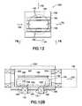
- FIG. 12is a top view of an exemplary cart of the substrate processing apparatus in accordance with another embodiment of the apparatus.
- FIG. 12Ais another top view of the exemplary cart in FIG. 12 with the cart shown in an extended position;
- FIG. 12Bis an end view of the exemplary cart in FIG. 12 in a portion of a chamber of the apparatus;
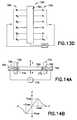
- FIG. 13Ais a top end view of a portion of a chamber of the apparatus with a drive system and transport cart in accordance with another embodiment of the apparatus;
- FIG. 13B-13Crespectively are a section view of the chamber and cart taken along lines 13 B- 13 B in FIG. 13A , and another section view taken along lines 13 C- 13 C in FIG. 13B ;
- FIG. 13Dis a schematic diagram of an exemplary drive system of the apparatus.
- FIG. 14Ais an end view of another embodiment of a cart used with the apparatus in FIG. 2 ;
- FIG. 14Bis a graph illustrating the relationship between axial deflection Z and a restoring force F of the drive system
- FIGS. 15-16are respectively a schematic perspective view and an exploded elevation view of semiconductor workpiece transport cart of the apparatus in accordance with another embodiment
- FIG. 17is a schematic perspective view of the transport cart in accordance with another embodiment.
- FIG. 18is a cross-section of a portion of the transport apparatus in FIG. 2 and a workpiece chuck rotation device of the apparatus;
- FIGS. 19-20respectively are elevation views of the workpiece chuck rotation device and a transport cart of the apparatus with the transport cart in different positions;
- FIG. 21is another schematic elevation of the chuck rotation device in accordance with yet another embodiment.
- FIGS. 22-23respectively are a schematic top plan view and schematic elevation view of yet another embodiment of the transport cart for the apparatus;
- FIGS. 23A-23Brespectively are other top plan views of the transport cart in FIG. 22 with a transfer arm of the cart in two different positions;
- FIG. 24is a schematic elevation view of another embodiment of the transport cart.
- FIGS. 24A-24Crespectively are plan views of the transport cart in FIG. 24 with the transport arm linkage of the cart in three different positions;
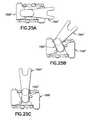
- FIG. 25is a schematic elevation view of still another embodiment of the transport cart.
- FIGS. 25A-25Crespectively are plan views of the transport cart in FIG. 25 with the transport arm linkage of the cart in three different positions;
- FIG. 26is a schematic diagram of system control software in the controller of the apparatus.
- FIG. 27is a schematic plan view of a substrate processing system in accordance with yet another exemplary embodiment of the invention.
- FIG. 28is a cross-sectional elevation view of a representative module of a transport chamber of the system in FIG. 27 ;
- FIG. 29is a cross-sectional view of the chamber module taken along line 29 - 29 in FIG. 28 ;
- FIG. 30is a bottom view of a substrate transport of the system in FIG. 27 .
- FIG. 2there is shown a schematic plan view of a substrate processing apparatus 10 incorporating features of the present invention.
- a substrate processing apparatus 10incorporating features of the present invention.
- the present inventionwill be described with reference to the embodiments shown in the drawings, it should be understood that the present invention can be embodied in many alternate forms of embodiments.
- any suitable size, shape or type of elements or materialscould be used.
- the substrate processing apparatus 10is connected to an environmental front end module (EFEM) 14 which has a number of load ports 12 as shown in FIG. 2 .
- the load ports 12are capable of supporting a number of substrate storage canisters such as for example conventional FOUP canisters; though any other suitable type may be provided.
- the EFEM 14communicates with the processing apparatus through load locks 16 which are connected to the processing apparatus as will be described further below.
- the EFEM 14(which may be open to atmosphere) has a substrate transport apparatus (not shown) capable of transporting substrates from load ports 12 to load locks 16 .
- the EFEM 14may further include substrate alignment capability, batch handling capability, substrate and carrier identification capability or otherwise.
- the load locks 16may interface directly with the load ports 12 as in the case where the load locks have batch handling capability or in the case where the load locks have the ability to transfer wafers directly from the FOUP to the lock.
- Some examples of such apparatusare disclosed in U.S. Pat. Nos. 6,071,059, 6,375,403, 6,461,094, 5,588,789, 5,613,821, 5,607,276, 5,644,925, 5,954,472, 6,120,229 and U.S. patent application Ser. No. 10/200,818 filed Jul. 22, 2002 all of which are incorporated by reference herein in their entirety.
- other lock optionsmay be provided.
- the processing apparatus 10which as noted before may be used for processing semiconductor substrates (e.g. 200/300 mm wafers), panels for flat panel displays, or any other desired kind of substrate, generally comprises transport chamber 18 , processing modules 20 , and at least one substrate transport apparatus 22 .
- the substrate transport apparatus 22 in the embodiment shownis integrated with the chamber 18 .
- processing modulesare mounted on both sides of the chamber.
- processing modulesmay be mounted on one side of the chamber as shown for example in FIG. 4 .
- processing modules 20are mounted opposite each other in rows Y 1 , Y 2 or vertical planes.
- the processing modulesmay be staggered from each other on the opposite sides of the transport chamber or stacked in a vertical direction relative to each other.
- the transport apparatus 22has a cart 22 C that is moved in the chamber to transport substrates between load locks 16 and the processing chambers 20 . In the embodiment shown, only one cart 22 C is provided, in alternate embodiments, more carts may be provided.
- the transport chamber 18(which is subjected to vacuum or an inert atmosphere or simply a clean environment or a combination thereof in its interior) has a configuration, and employs a novel substrate transport apparatus 22 that allows the processing modules to be mounted to the chamber 18 in a novel Cartesian arrangement with modules arrayed in substantially parallel vertical planes or rows.
- the transport chamber 22may be capable of being provided with any desired length to add any desired number of processing modules, as will be described in greater detail below, in order to increase throughput.
- the transport chambermay also be capable of supporting any desired number of transport apparatus therein and allowing the transport apparatus to reach any desired processing chamber on the transport chamber without interfering with each other. This in effect decouples the throughput of the processing apparatus from the handling capacity of the transport apparatus, and hence the processing apparatus throughput becomes processing limited rather than handling limited. Accordingly, throughput can be increased as desired by adding processing modules and corresponding handling capacity on the same platform.
- the transport chamber 18 in this embodimenthas a general rectangular shape though in alternate embodiments the chamber may have any other suitable shape.
- the chamber 18has a slender shape (i.e. length much longer than width) and defines a generally linear transport path for the transport apparatus therein.
- the chamber 18has longitudinal side walls 18 S.
- the side walls 18 Shave transport openings or ports 180 formed therethrough.
- the transport ports 180are sized large enough to allow substrates to pass through the ports (can be through valves) into and out of the transport chamber.
- the processing modules 20 in this embodimentare mounted outside the side walls 18 s with each processing module being aligned with a corresponding transport port in the transport chamber.
- each processing module 20may be sealed against the sides 18 S of the chamber 18 around the periphery of the corresponding transport aperture to maintain the vacuum in the transport chamber.
- Each processing modulemay have a valve, controlled by any suitable means to close the transport port when desired.
- the transport ports 180may be located in the same horizontal plane. Accordingly, the processing modules on the chamber are also aligned in the same horizontal plane. In alternate embodiments the transport ports may be disposed in different horizontal planes.
- the load locks 16are mounted to the chamber sides 18 S at the two front most transport ports 180 . This allows the load locks to be adjacent the EFEM 14 at the front of the processing apparatus.
- the load locksmay be located at any other transport ports on the transport chamber such as shown for example in FIG. 4 .
- the hexahedron shape of the transport chamberallows the length of the chamber to be selected as desired in order to mount as many rows of processing modules as desired (for example see FIGS. 3 , 5 , 6 - 7 A showing other embodiments in which the transport chamber length is such to accommodate any number of processing modules).
- the transport chamber 18 in the embodiment shown in FIG. 2has one substrate transport apparatus 22 having a single cart 22 C.
- the transport apparatus 22is integrated with the chamber to translate cart 22 C back and forth in the chamber between front 18 F and back 18 B.
- the transport apparatus 22has cart 22 C having end effectors for holding one or more substrates.
- the cart 22 C of transport apparatus 22also has an articulated arm or movable transfer mechanism 22 A for extending and retracting the end effectors in order to pick or release substrates in the processing modules or load locks.
- the transport apparatus 22may be aligned with desired module/port and the arm is extended/retracted through the corresponding port 180 to position the end effector inside the module/port for the substrate pick/release.
- the transport apparatus 22shown in FIG. 2 is a representative transport apparatus and, includes a cart 22 C which is supported from linear support/drive rails.
- the transport apparatuswill be described in greater detail below.
- the linear support/drive railsmay be mounted to the side walls 18 S, floor, or top of the transport chamber and may extend the length of the chamber. This allows the cart 22 C, and hence, the apparatus to traverse the length of the chamber.
- the carthas a frame, which supports the arm.
- the framealso supports caster mounts or platens 22 B, which move with or relative to the frame.
- a sequential synchronous linear motor 30drives the platens 22 B and hence the cart 22 C along the rails.
- the linear motor 30may be located in the floor or side walls 18 S of the transport chamber.
- a barriermay be located between the windings of the motor and the motive portion of the platens to isolate the windings from the interior of the chamber.
- the linear motormay include a number of drive zones.
- the drive zonesare located at locations along the transport chamber where the arm 22 A is extended/retracted (i.e. at the rows YO-Y 2 in this embodiment of modules/ports).
- the number and density of drive zonesis dependent on the number of platens per cart, the number of motors per chamber, the number of process modules or exchange points etc.
- the armis operably connected to the platens 22 A by a suitable linkage/transmission so that when the platens are moved by a drive motor in relative motion to each other the arm is extended or retracted.
- the transmissionmay be arranged so that when the platens are moved apart along the rails the arm is extended to the left, and when moved back closer together the arm is retracted from the left.
- the platensmay also be suitably operated by a linear motor to extend/retract the arm 22 A to/from the right.
- the control of movement of the platens over the slide rails with the linear motor, as well as position sensing of the platens and hence of the cart and the extended/retracted position of the armmay be accomplished in accordance with international application having publication numbers WO 99/23504; 99/33691; 01/02211; 01/38124; and 01/71684, which are incorporated by reference herein in their entireties.
- the platensmay be driven in unison in one direction in order to move the entire cart/apparatus in that longitudinal direction inside the transport chamber.
- FIG. 3shows another embodiment of a substrate processing apparatus 10 ′ which is generally similar to apparatus 10 .
- the transport chamber 18 ′has two transport apparatus 22 A, 22 B.
- the transport apparatus 122 A, 122 Bare substantially the same as the apparatus 22 in the previously described embodiment.
- Both transport apparatus 122 A, 122 Bmay be supported from a common set of longitudinal slide rails as described before.
- the platens of the cart corresponding to each apparatusmay be driven by the same linear motor drive.
- the different drive zones of the linear motorallow the independent driving of individual platens on each cart and thus also the independent driving of each individual cart 122 A, 122 B.
- the arm of each apparatuscan be independently extended/retracted using the linear motor in a manner similar to that described before.
- the substrate transport apparatus 122 A, 122 Bare not capable of passing each other in the transport chamber unless separate slide systems are employed. Accordingly, the processing modules are positioned along the length of the transport chamber so that the substrate may be transported to be processed in the processing module in a sequence which would avoid the transport apparatus from interfering with each other. For example, processing modules for coating may be located before heating modules, and cooling modules and etching modules may be located last.
- the transport chamber 18 ′may have another transport zone 18 ′A, 18 ′B which allow the two transport apparatus to pass over each other (akin to a side rail, bypass rail or magnetically suspended zone that does not require rails).
- the other transport zonemay be located either above or below the horizontal plane(s) in which the processing modules are located.
- the transport apparatushas two slide rails, one for each transport apparatus. One slide rail may be located in the floor, or side walls of the transport chamber, and the other slide rail may be located in the top of the chamber.
- a linear drive systemmay be employed which simultaneously drives and suspends the carts where the carts may be horizontally and vertically independently moveable, hence allowing them independent of each other to pass or transfer substrates.
- these windingsmay also be used as resistance heaters as in the case where it is desired that the chamber be heated for degas as in the case to eliminate water vapor for example.
- Each transport apparatus in this casemay be driven by a dedicated linear drive motor or a dedicated drive zone in which the cart resides similar to that described before.
- FIGS. 6 , and 7there are shown other substrate processing apparatus in accordance with other embodiments of the present invention.
- the transport chamber in these embodimentsis elongated to accommodate additional processing modules.
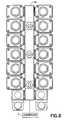
- the apparatus shown in FIG. 6has twelve (12) processing modules connected to the transport chamber, and each apparatus (two apparatus are shown) in FIG. 7 has 24 processing module connected to the transport chamber.
- the numbers of processing modules shown in these embodimentsare merely exemplary, and the apparatus may have any other number of processing modules as previously described.
- the processing modules in these embodimentsare disposed along the sides of the transport chamber in a Cartesian arrangement similar to that previously discussed. The number of rows of processing modules in these case however have been greatly increased (e.g. six (6) rows in the apparatus of FIG.
- the transport chamber of the apparatus in FIGS. 6 , and 7have multiple transport apparatus (i.e. three apparatus in the case of FIG. 6 , and six apparatus in the case of FIG. 7 ) to handle the substrates between the load locks and the processing chambers.
- the number of transport apparatus shownare merely exemplary and more or fewer apparatus may be used.
- the transport apparatus in these embodimentsare generally similar to that previously described, comprising an arm and a cart. In this case, however, the cart is supported from zoned linear motor drives in the side walls of the transport chamber.
- the linear motor drives in this caseprovide for translation of the cart in two orthogonal axis (i.e. longitudinally in the transport chamber and vertically in the transport chamber).
- the transport apparatusare capable of moving past one another in the transport chamber.
- the transport chambermay have “passing” or transport areas above and/or below the plane(s) of the processing modules, through which the transport apparatus may be routed to avoid stationary transport apparatus (i.e. picking/releasing substrates in the processing modules) or transport apparatus moving in opposite directions.
- the substrate transport apparatushas a controller for controlling the movements of the multiple substrate transport apparatus.
- the substrate processing apparatus 18 A and 18 B in this casemay be mated directly to a tool 300 .
- the transport chamber 18may be extended as desired to run throughout the processing facility P.
- the transport chambermay connect and communicate with various sections or bays, 18 A, 18 B in the processing facility P such as for example storage, lithography tool, metal deposition tool or any other suitable tool bays.
- bays interconnected by the transport chamber 18may also be configured as process bays or processes 18 A, 18 B.
- Each bayhas desired tools (e.g. lithography, metal deposition, heat soaking, cleaning) to accomplish a given fabrication process in the semiconductor workpiece.
- the transport chamber 18has processing modules, corresponding to the various tools in the facility bays, communicably connected thereto, as previously described, to allow transfer of the semiconductor workpiece between chamber and processing modules.
- the transport chambermay contain different environmental conditions such as atmospheric, vacuum, ultra high vacuum, inert gas, or any other, throughout its length corresponding to the environments of the various processing modules connected to the transport chamber.
- the section 18 P 1 of the chamber in a given process or bay 18 A, 18 B, or within a portion of the baymay have for example, one environmental condition (e.g. atmospheric), and another section 18 P 2 , 18 P 3 of the chamber may have a different environmental condition.
- the section 18 P 1 , 18 P 2 , 18 P 3 of the chamber with different environments thereinmay be in different bays of the facility, or may all be in one bay of the facility.
- FIG. 7shows the chamber 18 having three sections 18 P 1 , 18 P 2 , 18 P 3 with different environments for example purposes only.
- the chamber 18 in this embodimentmay have as many sections with as many different environments as desired.
- the transport apparatussimilar to apparatus 122 A, (see also FIG. 3 ) in the chamber 18 are capable of transiting between sections 18 P 1 , 18 P 2 , 18 P 3 of the chamber with different environments therein.
- the transport apparatus 122 Amay with one pick move a semiconductor workpiece from the tool in one process or bay 18 A of the processing facility to another tool with a different environment in a different process or bay 18 B of the process facility.
- transport apparatus 122 Amay pick a substrate in processing module 301 , which may be an atmospheric module, lithography, etching or any other desired processing module in section 18 P 1 , of transport chamber 18 .
- the transport apparatus 122 Amay then move in the direction indicated by arrow X 3 in FIG. 7 from section 18 P 1 of the chamber to section 18 P 3 .
- the transport apparatus 122 Amay place the substrate in processing module 302 , which may be any desired processing module.
- the transport chambermay be modular, with chamber modules connected as desired to form the chamber 18 .
- the modulesmay include internal walls 18 I, similar to walls 18 F, 18 R in FIG. 2 , to segregate sections 18 P 1 , 18 P 2 , 18 P 3 , 18 P 4 of the chamber.
- Internal walls 18 Imay include slot valves, or any other suitable valve allowing one section of the chamber 18 P 1 , 18 P 4 to communicate with adjoining section.
- the slot valves 18 Vmay be sized to allow, one or more carts to transit through the valves from one section 18 P 1 , 18 P 4 to another. In this way, the carts 122 A may move anywhere throughout the chamber 18 .
- the valvesmay be closed to isolate sections 18 P 1 , 18 P 2 , 18 P 3 , 18 P 4 of the chamber so that the different sections may contain disparate environments as described before. Further, the internal walls of the chamber modules may be located to form load locks 18 P 4 as shown in FIG. 2 .
- the load locks 18 P 4(only one is shown in FIG. 2 for example purposes) may be located in chamber 18 as desired and may hold any desired number of carts 122 A therein.
- processes 18 A and 18 Bmay be the same process, for example etch, where the processing apparatus 18 A and 18 B in combination with tool 300 being a stocker are capable of processing equal amounts of substrates as, for example the apparatus shown in FIG. 9 but without the associated material handling overhead associated with transporting FOUPS from the stocker to individual process tools via an AMHS, and transporting individual wafers via EFEM's to the respective processing tools.
- the robot within the stockerdirectly transfers FOUPS to the load ports (3 shown per tool, more or less could be provided depending on throughput requirements) where the wafers are batch moved into locks and dispatched to their respective process module(s) depending on the desired process and/or throughput required.
- the FIG. 7 apparatus and FIG. 9 apparatusmay have the same throughput, but the apparatus in FIG. 7 does it with less cost, lower footprint, less WIP required—therefor less inventory and with a quicker turnaround when looking at the time to process a single carrier lot (or “hot lot”) resulting in significant advantages for the fab operator.
- the stocker 300may further have metrology capability, sorting capability, material identification capability, test capability, inspection capability (put boxes etc. as required to effectively process and test substrates.
- more or less processes 18 A and 18 Bmay be provided that are different processes, for example etch, CMP, copper deposition, PVD, CVD, etc.
- the processing apparatus 18 A, 18 B, etc. in combination with tool 300 being, for example a photolithography cellare capable of processing equal amounts of substrates as, for example multiple apparatus' shown in FIG. 9 but without the associated material handling overhead associated with transporting FOUPs from stockers to individual process tool bays and a lithography bay via an AMHS, and transporting individual wafers via EFEM's to the respective processing tools.
- the automation within the lithography celldirectly transfers FOUPS, substrates or material to the load ports (3 shown per process type, more or less could be provided depending on throughput requirements) where the substrates are dispatched to their respective process depending on the desired process and/or throughput required.
- An example of such an alternativeis shown in FIG. 7A .
- the apparatus in FIG. 7processes substrates with less cost, lower footprint, less WIP required—therefor less inventory and with a quicker turnaround when looking at the time to process a single carrier lot (or “hot lot”), and with a higher degree of contamination control resulting in significant advantages for the fab operator.
- the tool 18 A, 18 B or the tool or cell 300may further have metrology capability, processing capability, sorting capability, material identification capability, test capability, inspection capability (put boxes . . . ) etc . . . as required to effectively process and test substrates.
- the processing apparatus 18 A, 18 B, and tool 300may be coupled to share a common controller environment (e.g. inert atmosphere, or vacuum). This ensures that substrates remain in a controlled environment from tool 300 and throughout the process in apparatus 18 A, 18 B. This eliminates use of special environment controls of the FOUPs as in conventional apparatus configuration shown in FIG. 8 .
- FIG. 7Athere is shown an exemplary fabrication facility layout 601 incorporating features of the embodiment shown in FIG. 7 .
- Carts 406similar to carts 22 A, 122 A transport substrates or wafers through process steps within the fabrication facility 601 through transport chambers 602 , 604 , 606 , 608 , 610 , 612 , 614 , 616 , 618 , 620 , 624 , 626 .
- Process stepsmay include epitaxial silicon 630 , dielectric deposition 632 , photolithography 634 , etching 636 , ion implantation 638 , rapid thermal processing 640 , metrology 642 , dielectric deposition 644 , etching 646 , metal deposition 648 , electroplating 650 , chemical mechanical polishing 652 .
- more or less processesmay be involved or mixed; such as etch, metal deposition, heating and cooling operations in the same sequence.
- carts 406may be capable of carrying a single wafer or multiple wafers and may have transfer capability, such as in the case where cart 406 has the capability to pick a processed wafer and place an unprocessed wafer at the same module.
- Valves 654may be sealed valves or simply conductance type valves depending upon the pressure differential or gas species difference on either side of a given valve 654 . In this manner, wafers or substrates may be transferred from one process step to the next with a single handling step or “one touch”. As a result, contamination due to handling is minimized. Examples of such pressure or species difference could be for example, clean air on one side and nitrogen on the other; or roughing pressure vacuum levels on one side and high vacuum on the other; or vacuum on one side and nitrogen on the other.
- Load locks 656similar to chambers 184 P 4 in FIG.
- Load locks 656may be capable of transitioning a single carrier or multiple carriers.
- substrate(s)may be transferred into load lock 656 on shelves (not shown) or otherwise where the cart is not desired to pass through the valve.
- Additional features 658such as alignment modules, metrology modules, cleaning modules, process modules (ex: etch, deposition, polish etc . . . ), thermal conditioning modules or otherwise, may be incorporated in lock 656 or the transport chambers.
- Service ports 660may be provided to remove carts or wafers from the tool.
- Wafer or carrier stockers 662 , 664may be provided to store and buffer process and or test wafers. In alternate embodiments, stockers 662 , 664 may not be provided, such as where carts are directed to lithography tools directly. Another example is where indexer or wafer storage module 666 is provided on the tool set.
- Re-circulation unit 668may be provided to circulate and or filter air or the gas species in any given section such as tool section 612 .
- Re-circulation unit 668may have a gas purge, particle filters, chemical filters, temperature control, humidity control or other features to condition the gas species being processed.
- Isolation stages 670may be provided to isolate carts and/or wafers from different process' or tool sections that can not be cross contaminated.
- Locks or interconnects 672may be provided to change cart orientation or direction in the event the cart may pick or place within a generic workspace without an orientation change. In alternate embodiments or methods any suitable combination of process sequences or make up could be provided.
- Drive system 320is an example of a drive suitable for driving transport apparatus or carts 22 A, 122 A, 406 shown in FIGS. 2 , 3 , and 7 - 7 A.
- System 320has a stationary winding set which drives platen 324 .
- Platen 324may be supported on slide blocks 326 which are slideable on rails 328 .
- Rails 328are coupled to a base 330 , or side walls, of the transport chamber.
- Base 330provides a barrier 332 between winding 322 and platen 324 . As can be realized, barrier 332 may also isolate the winding 322 from the interior environment of the chamber.
- Winding 322is coupled to base 330 .
- Platenmay have magnets 334 coupled to it for interfacing the platen 324 with winding 322 .
- a sensor 336may be a magneto-restrictive type hall effect sensor and may be provided for sensing the presence of the magnets in platen 324 and determining proper commutation. Additionally, sensors 336 may be employed for fine position determination of platen 324 .
- Position feedback device 340may be provided for accurate position feedback. Device 340 may be inductive or optical for example. In the instance where it is inductive, an excitation source 342 may be provided which excites winding or pattern 346 and inductively couples back to receiver 344 via coupling between pattern 346 . The relative phase and amplitude relationship used for determining the location of platen 324 .
- a cart identification tag 347such as an IR tag may be provided with a reader 348 provided at appropriate stations to determine cart id by station.
- FIG. 11Athere is shown an end view of platen drive system 400 in accordance with another embodiment.
- FIG. 11Bthere is shown a section view of drive system 400 , taken along lines 11 B- 11 B in FIG. 11A .
- system 400is capable of effecting movement of a platen or cart 406 (cart 406 may be similar to carts or transport apparatus 22 A, 122 A described before).
- System 400has opposing stationary winding sets 402 , 404 which drive cart 406 . Winding sets 402 , 404 are wound in a two dimensional driving array, vertical 408 and lateral 410 .
- additional arrayscould be provided to drive cart 406 in different directions, for example 427 by coupling system 400 to another similar system oriented 90 degrees therefrom.
- the arraysare driven in multiple zones in order to allow multiple carts to be driven independently.
- zone 424could be a supply zone
- zone 426could be a transfer zone
- zone 428could be a return zone.
- Within each zonemay be sub-zones which allow driving multiple carts within each zone. In alternate embodiments, more or less zones or sub-zones may be provided in any of a number of combinations.
- Cart 406is supported by the fields produced by winding sets 402 , 404 and is positionable in a non-contact manner by biasing the fields between winding sets 402 and 406 .
- Chamber 412may be provided as a barrier 414 between winding sets 402 , 404 and cart 406 .
- Windingsexist in zone 416 as shown.
- Cart 406may have platens 418 , 420 with the windings. In alternate embodiments, more or less platens may be provided.
- Arrays of sensorsmay be provided for sensing the presence of the magnets in the platens or the cart or the platens for determining proper commutation and location and for fine position determination of the platens and the cart.
- a cart identification tagmay be provided with a reader provided at appropriate stations to determine cart id by station.
- Cart 229may be similar to carts 22 , 122 A, 406 described before and shown in FIGS. 2 , 3 , and 7 - 7 A.
- Cart 229is shown as being capable of transporting substrate 148 along an axial path 150 and/or a radial path 152 .
- the cart 229is also capable of moving the substrate along path 154 shown in FIG. 12 .
- Cart 229is shown as a two dimensional system for simplicity, however in alternate embodiments additional axis of motion, for example, z motion (not shown-in and out of paper) or angular motion 154 could be provided.
- Cart 229is shown as being capable of handling a single substrate 148 for simplicity. However, in alternate embodiments, additional handling could be provided.
- the cartmay include capability to handle a second substrate, as in the case where it is desired that a substrate be exchanged at a process module (i.e. a first, processed substrate may be picked and a second unprocessed substrate may then be placed at the same process module from the same cart 229 ).
- Cart 229has frame 156 , end effector 158 and secondary frame 160 .
- Slides 162constrain frame 156 , end effector 158 and secondary frame 160 to be slideable relative to each other along linear path 152 either to the left or right of frame 156 as shown.
- a linear mechanismis shown, in alternate embodiments, any suitable arm system may be used such as, for example, a scara type arm coupled to frame 156 as shown in FIG. 17 and as will be described in greater detail below.
- Substrate 148is supported on end effector 158 .
- FIG. 12Athere is shown a top view of exemplary cart 229 , in a portion of chamber 229 (similar to chamber 18 and 602 - 626 , see FIGS. 2-3 , and 7 - 7 A).
- the carthas the end effector 158 extended into exemplary module 166 .
- Module 166may be similar to any of the modules described before as being connected to the transport chamber.
- Cart 229is shown as being capable of transporting substrate 148 along an axial path 150 and/or a radial path 152 .
- Cart 229has frame 156 , end effector 158 and secondary frame 160 .
- Slides 162constrain frame 156 , end effector 158 and secondary frame 160 to be slideable relative to each other along linear path 152 either to the left or right of frame 156 as shown.
- Frame 156has magnetic platens 168 on its underside which interface with synchronous motor 170 .
- Drive platen 172interfaces with synchronous motor 174 .
- Drive platen 172is mounted on the underside of and slideable relative to frame 156 along direction 176 which is substantially parallel to direction 150 by using bearings 178 . Movement of platens 168 and 172 simultaneously along direction 150 allows cart to move in direction 150 without motion in direction 152 . Holding platens 168 stationary while simultaneously moving platen 172 along direction 176 relative to frame 156 causes a radial motion along direction 152 of substrate and end effector 148 , 158 .
- Pulley 186is rotatably coupled to frame 156 and has secondary pulleys 188 and 182 .
- Pulley 182is coupled to platen 172 with bands 184 such that movement of platen 172 along direction 180 causes pulley 182 to rotate in direction 190 with the opposite applying in opposing directions.
- Pulleys 192 and 194are rotatably coupled to frame 156 .
- Cable 196is coupled to pulley 188 at point 198 , wraps around pulley 192 as shown, and terminates at 200 on secondary frame 160 .
- Cable 202is coupled to pulley 188 at point 198 , wraps around pulley 188 counterclockwise, wraps around pulley 194 as shown and terminates at 204 on secondary frame 160 . In this manner, linear motion of platen 172 in direction 176 is translated into linear motion of secondary frame 160 along direction 152 .
- Linear motion of platen 172 in direction 176 and the translated linear motion of secondary frame 160 along direction 152also further extends end effector 158 in direction 152 as shown.
- Pulleys 210 and 212are rotatably coupled to secondary frame 160 .
- Cable 214is coupled to end effector 158 at point 216 , wraps around pulley 210 as shown, and terminates at 218 on frame 156 .
- Cable 220is coupled to end effector 158 at point 222 , wraps around pulley 212 and terminates at 224 on frame 156 .
- linear motion of platen 172 in direction 176is translated into linear motion of secondary frame 160 along direction 152 which is further translated to further extension of end effector 158 in direction 152 as shown.
- the transmissions between platens and end effectorsmay use belts, bands or any other suitable transmission means made of any suitable materials.
- a suitable linkage systemmay be used in place of cable pulleys to transmit motion from the platens to the end effectors. Retraction of the end effector 158 , to the position shown substantially in FIG. 12 , is accomplished in a similar but reverse manner. Further, extension of the end effector 158 to a position similar to but opposite from that shown in FIG. 12B is effected by moving platens 168 , 172 in an opposite manner to that described above.
- FIG. 12Bthere is shown an end view of cart 229 before being extended into exemplary process module 166 .
- Slides 240constrain frame 156 to be slideable along linear path 150 as shown.
- Frame 156has magnetic platens 168 on its underside which interface with synchronous motor 170 .
- Drive platen 172interfaces with synchronous motor 174 .
- Drive platen 172is mounted on the underside of and slideable relative to frame 156 along a direction which is substantially parallel to direction indicated by arrow 150 (see FIG. 12 ). Movement of platens 168 and 172 simultaneously along direction 150 allows the cart to move in direction indicated by arrow 150 without motion in direction 152 .
- Platens 172 and 168may have magnets that interface with motors 170 and 174 .
- Chamber 244may be made from a nonmagnetic material, for example non-magnetic stainless steel and provide a barrier 246 , 248 between the motor windings and their respective platens.
- more or less linear drives or cartsmay be provided.
- a single drive motormay be provided having additional drive zones where platens 168 and 172 would interface with the same drive motor but be independently driveable by the different zones.
- additional cartscould be driven by different drive systems in the floor 250 , the walls 252 , 254 above in line with or below the slot openings or in the cover 256 of the chamber.
- Chamber 716is another representative portion of chamber 18 , or chambers 602 - 624 of the apparatus (see FIGS. 2-3 , and 7 - 7 A).
- Cart 700is shown as being capable of transporting substrates 702 A, 702 B along an axial path 704 and/or a radial path 706 or in a Z motion (not shown-in and out of paper). In alternate embodiments, angular motion could be provided. In alternate embodiments, more or less substrate handling could be provided.
- Cart 700has transport mechanisms 724 A and 724 B which can be a linear mechanism or any suitable arm system may be used such as, for example, a scara type arm. In alternate embodiments no arm may be provided. Transport mechanisms 724 A and 724 B may extended into process modules or other modules as desired in a manner similar to that shown in FIG. 12A .
- Cart 700has platens 722 , 720 , 710 and 712 on its sides which interface with synchronous motors in the walls of transport chamber 716 .
- Drive platen 712is mounted on the side of cart 700 and is slideable relative to cart 700 along direction 704 . Platen 712 drives mechanism 724 A such that the movement of platen 712 along direction 704 (from location 712 A to 712 B, see FIG.
- drive platen 710is mounted on the side of cart 700 and is slideable relative to cart 700 along direction 704 .
- Platen 710drives mechanism 724 B such that the movement of platen 710 along direction 704 (from location 710 A to 710 B, see FIG. 13A ) relative to cart 700 allows mechanism 724 B to transport wafer 702 B between location 708 A and 708 B through slots 718 A and 718 B.
- Platens 710 and 712are independently moveable relative to cart 700 .
- Platens 722 , 720are fixed relative to cart 700 .
- Holding platens 720 , 722 stationary while simultaneously moving platen 712 along direction 704causes a radial transfer motion along direction 706 .
- Holding platens 720 , 722 stationary while simultaneously moving platen 710 along direction 704also causes a separate radial transfer motion along direction 706 .
- Simultaneously moving platens 720 , 722 , 710 and 712 along direction 704causes cart 700 to move along direction 704 —enabling the cart 700 to move from process location to process location as through valve 714 for example.
- FIG. 13Bthere is shown a section view of the exemplary drive system 701 and cart 700 taken along line 13 B- 13 B in FIG. 13A .
- FIG. 13Cthere is shown another side section view of the exemplary drive system 701 in FIG. 13B .
- System 701has opposing stationary winding sets 727 , 729 that drive cart 700 .
- Winding sets 727 , 729are wound in a combination of one and two dimensional driving arrays, for example, vertical 705 and lateral 704 .
- the driving arraysmay be linear motors or linear stepping type motors in one or two dimensional arrays. Examples of such driving arrays are described in U.S. Pat. Nos.
- zone 685could be a supply zone
- zone 683could be a transfer zone
- zone 681could be a return zone.
- FIG. 13Cshows one possible winding combination that could be driven by the system shown in FIG. 13D and employed to levitate cart 700 (as for example as discussed further below with reference to FIG. 14A , or through multiple axis active levitation).
- Cart 700has platens 720 and 710 which may be used in combination with arrays 738 B for platen 720 and arrays 736 B,C and D for platen 710 . By moving platen 710 in direction 704 (see FIG. 13A ) and holding platen 720 stationary, a wafer may be radially moved through slot 718 A.
- Chamber 716may be provided as a barrier between winding sets 727 , 729 and cart 700 .
- more or less platens or windingsmay be provided.
- Arrays of sensors 746 , 747 , 748may be provided for sensing the presence of the magnets in the platens or the platens or the cart(s) for determining proper commutation and location and for fine position determination of the platens and the cart or for determining positions, such as the gap between platens and windings.
- a cart identification tagas noted before, may be provided with a reader provided at appropriate stations to determine cart id by station.
- FIG. 14Athere is shown an end view of another exemplary cart 760 , in accordance with yet another embodiment, supported by the fields produced by single axis linear motor winding sets 762 , 764 .
- Exemplary cart 760is positionable in a non-contact manner by biasing 776 the fields between winding sets 762 and 764 .
- Position sensing 766 , 768is provided, in a close loop fashion with biasing 776 , to levitate cart 760 .
- Levitationmay be accomplished in this simple manner as the cart is passively stabilized in the Z direction as shown in FIG. 14B .
- Cart 760has magnetic platens 772 and 774 on its sides which may have magnets or be made from magnetic or conductive materials which interface with winding sets 762 , 764 . In alternate embodiments, more or less platens could be provided, driving arms for example.
- Chamber 770(similar to any representative portion of the chambers 18 , 602 - 624 of the apparatus, see FIGS. 2-3 , and 7 - 7 A) may be made from a nonmagnetic material, for example non-magnetic stainless steel and provide a barrier between the motor windings and their respective platens as described before. In alternate embodiments, more or less linear drives or carts may be provided.
- a single drive motormay be provided having additional drive zones where platens would interface with the same drive motor but be independently driveable by the different zones.
- additional cartscould be driven by different drive systems in the floor, the walls above in line with or below slot openings or in the covers of the chamber.
- FIG. 14Bthe relationship between the restoring force F and the axial deflection Z from the desired position of cart 760 is graphically illustrated.
- the restoring forcefirst increases in magnitude to a value FMAX or ⁇ FMAX respectively up to a maximal deflection ZMAX or ⁇ ZMAX respectively, but decreases again however when this deflection is exceeded. Therefore, if a force is applied to cart 760 (such as cart weight or external forces, such as from other winding sets that drive the same or other platens or otherwise) that exceeds FMAX, then the cart escapes from the windings 762 , 764 . Otherwise, cart 760 will stay within the fields as long as they are applied.
- Winding drive system 790has windings 792 , multiplexer 793 and amplifier modules 794 .
- Windings 792may have windings and/or sensors such as hall sensors, positions sensors, inductive sensors, carrier identification sensors, status and fault detection logic and circuitry or otherwise.
- Amplifier modules 794may have single or multiple phase amplifiers, position and/or presence sensor inputs or outputs, CPUs and/or memory, identification reader inputs or outputs, status and fault detection logic and circuitry or otherwise. Amplifier modules 794 may connect directly to windings 792 or through multiplexer unit 793 .
- amplifiers A 1 -Ammay be selectively connected to any of windings W 1 -Wn.
- a CPUcoordinates this selective connection and monitors the status of the devices. In this manner, the CPU may selectively take amplifier modules or windings off line for service without shutting down the tool.
- the transport apparatus or carts suitable for use in the transport chambers 18 , 602 - 624may comprise carts with or without a transfer arm for transferring semiconductor workpieces between the cart and a desired location in the apparatus.
- FIGS. 12 and 13Arespectively show, as described before, two exemplary embodiments of transport carts 229 , 700 with transfer arms for handling semiconductor workpieces in the apparatus.
- FIGS. 22 and 23there is shown another embodiment of a transport cart mechanism 1557 suitable for use in the chambers of apparatus 10 .
- Cart 1557may include base section or base plate 1558 and transfer arm 1577 mounted to the base plate. As shown in FIG.
- the cart mechanism base plate 1558with two coupled magnet arrays 1502 on opposite sides of the plate, but not limited to opposite corners of the plate.
- two addition magnet arrays 1502are coupled to linear bearing carriages 1560 and are made to slide on linear bearing rails 1562 .
- These linear bearing rails 1562are coupled to the base plate 1558 .
- a drive belt 1564 or other means of converting linear motion to rotary motionis attached to the linear bearing carriage 1560 .
- the drive belt 1564is wrapped around an idler pulley 1566 and then a pulley tensioner 1568 and attached to a drive pulley 1570 .
- the linear bearing/magnet array 1560 / 1502 and the coupled magnet array/cart base plate 1502 / 1558are driven as a fixed set and no rotation of the driven pulleys 1570 & 1572 is seen.
- the drive mechanism of base plate 1558may be used for operating other suitable transfer arm linkages, some examples are shown in FIGS. 24-24C , 25 - 25 C).
- the transfer arm 1577 in the embodiment shown in FIG. 23has a general single SCARA arm configuration.
- Drive pulley 1572is coupled to the lower link arm 1574 and drive pulley 1570 is tied to forearm drive pulley 1586 .
- the rotation motion of the forearm pulley 1586is coupled to the forearm 1578 through the drive belt 1582 and the elbow pulley 1576 .
- the wrist/end effector 1584is driven by the resulting relative rotation motion of the forearm 1578 with respect to the wrist elbow pulley 1580 as it is grounded to the lower link arm 1574 .
- this motionis achieved by the pulley ratio at each joint with respect to the input drive ratio of pulleys 1572 and 1570 .
- the transfer arm linkage 1577is shown respectively in retracted and extended positions. The movement between retracted and extended positions is achieved (in a manner as described above) by moving the movable magnet arrays 1502 as desired relative to the base plate.
- FIGS. 23A-23Bshow the transfer arm 1577 positioned so that when extended the arm 1577 extends to the lateral side 1576 R (i.e. the side of the cart facing a chamber wall) of the cart. This is similar to the extension/retraction movement of the transfer mechanism 724 A,B of cart 700 in FIG. 13A .
- the transfer arm 1577 on cart 1557may be rotated as a unit (using movable magnet arrays 1502 ) about axis of rotation S (see FIG. 22 ) to any desired orientation relative to the cart base plate. For example, if rotated about 180° from the orientation shown in FIGS.
- the transfer arm 1577may be extended to the opposite side 1575 L from that shown in FIG. 23B . Further, the transfer arm may be rotated about 90° so that the arm extension is along the linear direction of the chamber (indicated by arrow 15 X in FIG. 22 ). Any number of arm linkages may be employed with such a cart. Other examples of suitable arm linkages that may be used with the cart are described in U.S. Pat. Nos. 5,180,276; 5,647,724; 5,765,983; and 6,485,250 all incorporated by reference herein in their entirety.
- FIG. 24is an elevation view of another embodiment of the cart mechanism 1557 ′ with dual rotary end effectors mounted to the cart base plate 1558 ′.
- Cart 1557 ′is otherwise similar to cart 1557 described before and shown in FIGS. 22-23 . Similar features are similarly numbered.
- FIGS. 24A-24Cshow the use of both linear transport and couple relative motion of the bearing carriage array as the cart is moving. As described before with reference to FIG. 22 , the rotation of pulleys 1570 ′ and 1572 ′ results from the bearing carriage and magnet array moving with respect to the fixed magnet arrays which are coupled to the cart's base plate.
- the robot cart transportis moving along the linear chamber, in the direction indicated by arrows 15 X′, and the bearing carriage and magnet array move with respect to the grounded arrays.
- This motionenables the end effector (s) 1588 ′ and 1590 ′ to rotate thereby causing the robot end effector to extend substantially perpendicular to the linear direction of the cart similar to FIGS. 23A-23B , described before.
- FIGS. 24A-24Cshow the end effectors 1588 ′ and 1590 ′ extended to one side for example purposes. As can be realized however, the end-effectors 1588 ′, 1590 ′ may be extended to any side of the base plate.
- end effectors 1588 ′, 1590 ′may be extended to any side of the base plate. Further, the end effectors 1588 ′, 1590 ′ may be extended to a position where the end effector is oriented at an angle more or less than about 90° as shown in FIGS. 24A-24C .
- FIG. 25is a schematic elevation view of still another embodiment of the cart 1557 ′′, having and arm linkage similar to that shown in FIG. 23 .
- the drive pulley 1572 ′′is attached to the lower link arm 1592 ′′.
- the driver pulley 1570 ′′is coupled to the end effector driver pulley 1600 ′′ and coupled to the elbow pulley 1596 ′′ through a drive belt 1598 ′′.
- the elbow drive pulleyis attached to the robot end effector 1594 ′′ and provides a means of transmitting the rotation of driver pulley 1570 ′′ to the driven end effector 1594 ′′.
- FIGS. 25A-25Cshow the cart with the arm linkage in three different positions. FIGS.
- 25A-25Cshow the end effector 1594
- cartssuch as carts 22 , 122 A, 406 , 229 , 700 , 1557 , 1557 ′, 1557 ′′ shown in FIGS.
- the transfer chambermay be provided with the minimum width.
- the multi-axis articulation of the transfer arms on the different cart embodimentsallows substantially independent placement of the cart relative to the path of the articulating arm, which in turn allows the width of the transport chamber 18 to be reduced to a minimum.
- the width of slot valves and passages connecting storage processing modules to the transport chambermay be reduced to minimum size.
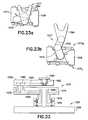
- the wafer aligner carrier 500may generally include two parts, wafer chuck 504 and the wafer transport carrier 502 .
- the alignerprovides wafer alignment and movement within the linear Cartesian transport tool.
- the aligneris made to interface with the transport cart(s) in the apparatus (such as for example carts 22 , 122 A, 406 , 700 , 1557 ) or in some cases may be included in the robot cart of the linear process tool architecture.
- the wafer chuck 504is shown to be able to separate from the wafer transport carrier 502 . Friction pads may couple the two devices during transport throughout the linear Cartesian apparatus. When disassembled, the wafer chuck 504 is free to rotate with respect to the wafer transport carrier 502 .
- the wafer chuck 504provides a means of passive wafer edge support by using angle ramped wafer edge pads 508 with respect to the substrate (wafer) 506 .
- An additional feature as part of the wafer chuck 504is the relief beneath the wafer 506 for the ability of the robot arm cart to remove and place the wafer onto the wafer carrier 500 . This is identified as wafer removal clearance zone 510 .
- This method of wafer rotation with respect to the linear transport cartcan be applied directly to the robot's end effector.
- This methodis shown in FIG. 17 .
- the robot arm cart 534is configured so that the wafer chuck 504 is removable from the robot's end effector 536 . In this case, the chuck is free to be rotated to correct for any slight wafer notch orientation requirements based on drop off point changes found in the process modules or load locks.
- the wafer chuck rotation device 532is shown. At multiple points within the linear transport tool, these rotational wells can be deployed. This device is based on motor isolation techniques found in U.S. Pat. No. 5,720,590 which is hereby incorporated by reference in its entirety. In alternate embodiments, a conventional motor and seal combination may be used.
- a stationary motor 522is mounted to the linear transport chamber's base 530 .
- a vacuum isolation barrier 520is placed between the motor armature 540 and the magnet array 524 .
- the magnet arrayis mounted directly to the rotation shaft 542 . This allows for direct drive coupling into the vacuum system.
- a possible support bearing 518may be required but ideally, magnetic suspension is used.
- An optical encoder disc 526is attached to the rotation shaft 542 with the read head 528 placed in a location to provide position feedback to the controller for the rotation shaft's 542 angle.
- the aligner chuck 504is lowered onto the friction pads or kinematics pin(s) 516 . These pads/pins provide a means of wafer chuck 504 rotation once the wafer chuck 504 is disconnected from the wafer carrier 502 or the robot's end effector 536 . This same means of providing rotation can be applied to control the rotational position of a robotic arm link 538 applied as part of the robot arm carrier shown in FIG. 17 .
- the wafer transport carrier 500consisting of the wafer chuck 504 and the wafer transport carrier is moved to a position above the wafer chuck rotation device 532 .
- the wafer transport carrieris lowered such that the wafer chuck 504 is lifted off on the transport carrier 502 .
- a camera 544 located in the transport's chamber lid 546is able to look at the image of the wafer and identify the wafer's x-y position and the location angle of the wafer's notch.
- the wafer carriercan then be moved to provide x-y location change of the wafer chuck 504 with respect to the wafer transport carrier 502 and rotation can be provided to correct for notch alignment.
- FIG. 21Another option for the wafer chuck rotational drive when used as a method of robot arm carrier device is to allow rotational engagement while extending the robot link arm and requiring vertical axis of motion to allow for the substrate or wafer to be lowered/raised from the process module or load lock.
- a method of this approachis schematically shown in FIG. 21 .
- a stationary motor 522is mounted to a guided plate 548 .
- the guided plateis attached to the linear transport chamber's base 530 via a metal bellows 550 or other linear isolation seal (lip seal, o-ring, etc.).
- a vacuum isolation barrier 520is placed between the motor armature 540 and the magnet array 524 .
- the magnet arrayis mounted directly to the rotation shaft 542 . This allows for direct drive coupling into the vacuum system.
- a possible support bearing 518may be required but ideally, magnetic suspension is used.
- An optical encoder disc 526is attached to the rotation shaft 542 with the read head 528 placed in a location to provide position feedback to the controller for the rotation shaft's 542 angle.
- An additional guide roller 552 and the supporting structure 554 with end of travel stop 556allow the rotation drive to be held positioned as required to engage the wafer chuck or robot arm rather than using the linear wafer transport carrier 500 as the actuation device.
- the force of the bellowswill act as a spring and allows the rotational device to be engaged with various linear robot arm cart vertical elevations (such as during a pick or place) but over a practical limited vertical travel range.
- the friction pads or kinematics pin(s) 516Once the device is engaged the friction pads or kinematics pin(s) 516 . These pads/pins provide a means of wafer chuck 504 rotation once the wafer chuck 504 is disconnected from the wafer carrier 502 or the robot's end effector 536 as shown in FIG. 20 . This same means of providing rotation can be applied to control the rotational position of a robotic arm link 538 applied as part of the robot arm carrier shown in FIG. 17 .
- MESmanufacturing execution
- the MES system 2000comprises software modules 2002 - 2016 or options that enhance the capabilities of the MES.
- the modulesinclude a material control system (“MCS”) 2002 , a real time dispatcher (“RTD”) 2004 , a workflow or activity manager (“AM”) 2006 , an engineering data manager (“EDA”) 2008 and a computer maintenance management system (“CMMS”) 2010 .
- MCSmaterial control system
- RTDreal time dispatcher
- AMworkflow or activity manager
- EDAengineering data manager
- CMMScomputer maintenance management system
- the MES 2002allows manufacturers to configure their factory resources and process plans, track inventory and orders, collect and analyze production data, monitor equipment, dispatch work orders to manufacturing operators, and trace consumption of components into finished products.
- the MCS software module 2002allows the manufacturer to efficiently schedule individual carts (for example, carts 22 , 122 A, 406 , 228 , 700 , 1557 in FIGS. 2-3 , 7 - 7 A, 12 , 13 A and 22 ) to arrive at the processing tools to maximize overall system efficiency.
- the MCSschedules when an individual cart will arrive at, and depart from, a specified processing tool (for example, process 18 A, 18 B in FIG. 7 , and modules 602 - 626 in FIG. 7A ).
- the MCSmanages any queuing and routing requirements at each processing tool and optimizes the system yield while minimizing the cart transport cycle time.
- the RTD 2004allows manufacturers to make cart routing decisions, in real time, based on feed back from the health of the processing tools. Additionally, cart routing decisions may be made by the MES operator. The MES operator may change the priority in which specific products need to be manufactured.
- the AM 2006allows manufacturers to monitor the progress of any given cart containing one or more substrates though the entire manufacturing process.
- the AM 2006determines the best remaining route for the all the substrates being processed at the processing tool.
- the EDA 2008allows manufactures to analyze the manufacturing data and execute statistical process control algorithms on that data in an effort to improve the efficiency of the processing tool.
- the CMMS 2010 systemallows the manufacturer to predict when maintenance is required on an individual processing tool. Variances in the process of the processing tool is monitored and compared against known process results and changes to the process or scheduled repairs to the processing tool is predicted.
- FIG. 27there is shown a substrate processing system 3010 in accordance with yet another exemplary embodiment of the invention.
- the system 3010 in FIG. 27is generally similar to processing systems and tools 10 , 10 ′, 18 , 18 A, 18 B, 601 described before and shown in the drawings, except as otherwise noted below.
- System 3010generally includes substrate processing tool 3014 and in this embodiment tool interfaces 3012 and 3016 .
- tool 3018has a controlled atmosphere and is isolated from the outside atmosphere.
- the tool interfaces 3012 , 3016generally provide an interface between the tool 3014 and other cooperative systems in the fab.
- tool interface 3012may be an EFEM suitably configured for interaction with a fab mass substrate transport system 3001 , such as automated guided vehicles, or other desired automated material handling system.
- the EFEM 3012may be able to allow or provide for loading and offloading of substrates between the mass transport system 3001 and EFEM, and hold unprocessed substrates for entry (in the direction indicated by arrow 3000 S) into the processing tool 3018 .
- the EFEM 3012may also be capable of receiving from the processing tool 3018 (in the direction indicated by arrow 3000 P), processed substrates for return transfer to the fab transport system 3001 .
- system 3010has another tool interface 3016 , such as an environmental second end module (ESEM), at the opposite end of the tool 3018 from EFEM 3012 .
- ESEMenvironmental second end module
- ESEM 3016in this embodiment, is substantially similar to EFEM 3012 , capable for example of receiving processed substrates from the tool 3018 (in the direction indicated by arrow 3000 P in FIG. 27 ) and able to facilitate subsequent transfer of the substrates to an adjoining portion of fab transport system 3001 .
- ESEM 3016may also be used to feed unprocessed substrates to tool 3018 .
- the processing systemmay have a tool interface at but one of the tool ends. In that case, unprocessed substrates would be input, and processed substrates would be output, throughout the one end of the process tool where the tool interface is located.
- the toolmay interface or be otherwise connected directly to another tool or to a transport chamber having a controlled atmosphere (such as in a manner similar to that shown in FIG. 7A for transport chambers 602 - 626 ).
- tool 3018generally comprises a substrate transport chamber 3014 and process modules 3020 , 3020 A.
- chamber 3014may have a controlled atmosphere such as a vacuum or inert gas and may be isolated from the outside atmosphere.
- Transport chamber 3014may have different sections 3014 A, 3014 B, 3014 C, capable of being isolated from each other, such that each section may be capable of holding a different controlled atmosphere (e.g. vacuum, near high vacuum, high vacuum). As seen in FIG.
- the transport chamber 3014has a generally linear shape.
- the process modules 3026 , 3020 Aare mounted in this embodiment to the lateral sides of the transport chamber 3014 .
- the process modules 3020 , 3020 Amay be similar or different from each other.
- the processing tool 3018may have one or more load lock chamber modules 3020 A (in the embodiment shown in FIG. 27 there are four load lock chamber modules 3020 A, two of which communicate with each tool interface 3012 , 3016 ) as desired to allow transfer of substrates into and out of the tool (in the direction indicated by arrows 3000 I/O) without affecting the controlled atmosphere in the tool.
- the other process modulesmay be configured to perform desired processing on substrates in the tool, such as dielectric or metal deposition, etching, ion implantation, rapid thermal processing, chemical or mechanical polishing, metrology and others.
- the process modulesare connected to the sides of the transport chamber 3018 to form a seal with the chamber and maintain the controlled atmosphere in the chamber.
- the process modules 3020may be arranged in any desired order along the chamber 3014 , such as for example to provide a desired serial processing sequence when substrates progress through the tool in direction 3000 S.
- tool 3018does not limit the process sequence, to which substrates are subjected, to merely the serial order of the process modules arrangement on the tool, but rather allows selectability of the process steps.
- the process modules of the tool 3018may each provide substantially the same process.
- the tool 3018has at least one transport vehicle or cart 3229 located in chamber 3014 , and capable of holding one or more substrates thereon.
- the cart 3229is capable of linear traverse inside the chamber 3014 (in the direction indicated by arrow 3000 X).
- the cart 3229may also have a suitable operable substrate transfer device 3160 for transferring substrates between the cart, inside the transport chamber 3014 , and the process modules 3020 , 3020 A (in the direction indicated by arrow 3000 Y in FIG. 27 ).
- the cart 3229 in this embodimentis passive, without motors or powered systems.
- the transport chamber 3014includes a drive system 3400 that interfaces with the cart to move the cart within the chamber (direction 3000 X) and effect operation of the cart substrate transfer device 3160 to transfer substrates (indicated by direction 3000 Y).
- the transport chamber 3014may also include a position feed back system 3336 for identifying the position of the cart 3229 and substrate.
- the drive system 3400 and position feed back system 3336are operated by the CPU to move the cart and transfer substrates in order to select any desired process sequence for the substrates processed by the tool.
- the transport chamber 3014is formed by modules 3016 , 3016 A, 3016 B, 3016 C that are abutted to each other.
- each module 3016 , 3016 A, 3016 B, 3016 Cis a self contained unit with integral drive system and, position feed back system portion to allow each module to operate as an individual transport chamber, and to allow integration of any desired number of modules to form the transport chamber 304 of desired length.
- the transport chamber modules 3016 , 3016 A, 3016 B, 3016 C forming the transport chamber 3014are generally similar to each other.
- the transport chamber modules 3016 , 3016 A, 3016 B, 3016 Cmay have different lengths, and different numbers of connections for connection of any desired number of process chamber modules to each transport chamber module.
- each transport chamber moduleis capable of having a process chamber module 3020 , 3020 A connected to each side of the transport chamber module, in alternate embodiments transport chamber modules may be configured to interface with multiple process chamber modules similar to modules 3020 .
- the transport chamber modules 3016 , 3016 A, 3016 B, 3016 Care interchangeable so that the chamber modules may be joined together in any desired sequence to form the transport chamber.
- FIGS. 28 and 29are cross sectional views of an exemplary transport chamber module 3016 ( FIG. 29 further shows portions in phantom of adjacent transport chamber modules 3016 , 3016 A when abutted/mated to the chamber module 3016 ).
- the transport chamber modules 3016 , 3016 A, 3016 B, 3016 Care substantially similar.
- Chamber module 3016has a frame 3016 F, which may be of any suitable shape and made of any suitable material.
- the frame 3016 Fmay have removable panels or sections, such as for example removable top panel 3016 T.
- the removable panel 3016 Tis mounted to the rest of the module frame 3016 F to allow removal from the module when the module is connected to other modules forming the chamber.
- Access panel 3016 Tmay be sufficiently large to allow insertion/removal of the cart 3229 through the resultant opening 3016 O in the chamber module frame.
- a seal 3016 Sis provided at the interface of the panel 3016 T and frame to prevent compromise of the controlled atmosphere in the transport chamber 3014 .
- the framehas ports 3016 P formed therein for communication with the process chamber modules 3020 .
- the ports 3016 Pare sized and shaped to allow the substrate transfer device 3306 O with the substrate S thereon to pass through the port into the process module.
- the ports 3016 Pmay be closable by suitable valves or doors that may be integrated into the transport chamber module frame 3016 F, or may be mounted on the process module.
- the frame 3016 Fhas suitable interface features 3016 I at the opposite longitudinal ends for sealably mating the module 3016 to adjoining modules 3016 A, 3016 .
- the interfaces 3016 Imay be of any suitable type.
- the interfaces 3016 Imay have suitable seating features complementing mating facets of the adjoining module interface to allow proper abutment of the adjoining modules.
- Fastenerssuch as mechanical fasteners, or other suitable clamping or retention features may be included to capture the modules to each other.
- the interfaces 3016 I 1 , 3016 I 2may include polarization facets to establish a desired orientation of the chamber modules 3016 , 3016 A when being joined (and preventing abutment and connection therebetween when the module is not in the desired orientation) the interface features 3016 I 1 , 3016 I 2 are common to each module allowing the modules to be interchangeable as noted before.
- the frame 3016 Fin this embodiment defines a chamber space sufficient for cart 3229 . Minimum clearances may be provided around the cart to allow free movement of the cart through the module.
- the end openings 3016 R in the module frameare sized to allow the cart 3229 (holding a desired number of substrates S) to pass through the opening, and traverse between modules 3016 , 3016 A.
- the end openings 3016 Rmay be closed by doors 3016 D.
- the doors 3016 Dmay be integral with the module frame, or may be installed as an additional modular portion between chamber modules when the chamber modules are joined together.
- the modulehas support or guide rails 3040 for cooperating with slides 3240 on the cart, movably support the cart 3229 in the chamber.
- the rails 3040are located on the bottom of the module (under the cart), though in alternate embodiments the rails may be attached to any desired portion of the chamber module frame.
- two rails 3040are shown, but more or fewer rails may be used.
- the rails 3040are shown as extending continuously through the module.
- the rails 3040terminate at a distance 3040 D from the interfacing face of the module 3016 sized so that, when the cart passes between modules 3016 , 3016 A, the slides 3240 on the cart may traverse the distance 3040 D (in each module) and commence riding on the rail of the adjacent module 3016 , 3016 A without disturbance to the stable attitude of the cart.
- the slides 3240 of the cart 3229are sized to continue to provide stable support to the cart when the cart passes between modules 3016 , 3016 A and the slides 3240 traverse from the rails 3040 in one module 3016 , 3016 A to the adjoining rail segments in the adjoining module.
- the module 3016has an integral portion of the cart drive system 3400 .
- the systemis a linear electrical motor, though in alternate embodiments any suitable type of electric or mechanical drive system may be used such as a cable drive.
- the drive systemis a coreless linear drive system, such as coreless linear motors available from Tecnotion or Anorad.
- the drive system portion integral to the transport chamber module 3016is shown as having three sets of windings 3402 , 3402 A, 3402 B, 3404 , 3404 A, 3404 B on each side of the module. As seen in FIG.
- each set of windings 3402 , 3404cooperates with a corresponding platen 3168 , 3172 on the cart 3229 .
- the windings 3402 , 3404may be of any desired length, including commercially available standard lengths. In alternate embodiments, any desired number of windings may be used to drive the cart platens on each side of the chamber.
- the coreless motor windings 3402 , 3404project into the chamber to interface with the platen 3168 , 3172 of the cart.
- the linear motormay be an iron core linear motor similar to the motor 400 described before and shown in FIGS. 11A-11B . In that case, the motor windings may be isolated from the chamber by interior frame portions similar to portions 414 in FIGS.
- windings 340 L, 340 SA, 3402 B, and 3404 , 3404 A, 3404 B on each side of the moduleare arranged respectively along a single axis, thereby providing one drive axis on each side.
- windingsmay be positioned to provide multiple drive axes on each side.
- the windingsmay be arranged to provide drive axes in both X and Z directions (i.e. both linear along the chamber, as well as vertical drive axes, for shunting the cart between longitudinal drive axes, similar to the winding arrangement described before and shown in FIGS. 13B-13C ).
- Windings 3402 - 3402 B, and 3404 - 3404 B, along each drive axis,are also sized and positioned relative to the module interface 3016 I 1 , 3016 I 2 , to maintain, in cooperation with the next most proximate windings 3400 B in the abutting module 3016 , a continuous propulsive force on the platens traversing the interface region of the abutting modules, enabling the cart to traverse from one module 3016 , 3016 A to the other.
- a control system 3790controlled by the CPU is provided to control operation of the windings. Though in FIG.
- the winding control system 3790is generally similar to winding control system 790 , described before and shown in FIG. 13D .
- the winding control or drive system 3790may generally have a multiplexer 3793 and amplifier modules 3794 .
- the amplifier modules 3794may be connected via multiplexer 3793 to drive windings 3402 , 3402 A, 3402 B along each drive axis in the desired sequence for moving the cart platens. The sequencing and connection of the amplifiers to the windings is controlled by the CPU.
- the CPUmay communicate with the position feed back system 3336 of the module, as will be described further below, to determine the amplifier connection and drive sequence of the windings.
- the winding control system 3790may be a discrete system dedicated to the module 3016 .
- the control system 3790may be carried, mounted or otherwise incorporated with the module 3016 (the control system 3790 need not be positioned on the module frame, and may be enclosed in a separate housing (not shown) if desired).
- the control system 3790may communicate with the windings 3402 , 3402 A, 3402 B through suitable communication lines penetrating through the chamber when using suitable feed through. In FIG.
- FIG. 30here is shown a bottom view of the cart 3229 .
- the cartmay have any suitable configuration.
- the cartis substantially similar to cart 229 described before and shown in FIG. 12-12B .
- cart 3229has two platens 3168 , 3172 .
- Platens 3168 , 3172have permanent magnets or magnetic material, and are configured for operation with the coreless linear windings 3402 , 3404 as shown in FIG. 28 .
- Platen 3168 in this embodimentis fixedly mounted to the cart frame 3156 .
- Platen 3172is movably secured, such as by keyed slides 3156 S, to the frame 3156 of the cart.
- Platen 372is thus capable of limited movement relative to the cart frame 3156 (in the direction indicated by arrow 3229 X shown in FIG. 30 ). Fore and aft stops limit the motion of platen 3172 relative to the frame. Similar to platen 172 of cart 229 , described before, the additional mobility of the platen 317 L relative to cart 3229 , provide the cart with a further degree of freedom that is converted to operate the substrate transfer device 3160 in order to extend and retract. Substrate transfer device 3160 is substantially similar to the telescoping sections 158 , 160 of cart 229 (see FIGS. 12A , 12 B).
- transfer device 3160may include any suitable number of telescoping sections, terminating with an end effector, similar to end effector 158 described before.
- the transfer device 160may be connected by a suitable transmission system, similar to the system of cart 229 , to the movable platen 3172 to convert the relative movement of the platen to movement of the transfer device 3160 (and hence movement of the substrate in the direction indicated by arrows 3000 Y 1 , 3000 Y 2 in FIG. 28 ) (Z axis) may be generated by deenergizing/energizing the windings 3402 , 3404 and raising/lowering the cart to pick/place the substrate S.
- the substrate transfer device of the cartmay be of any suitable type such as for example a scara type arm, having one or more articulated sections. Further independent degrees of freedom, for independent motion of various transfer device sections may be provided by adding additional platens to the cart that are mounted to be independently movable relative to the cart similar to platen 3172 .
- the cartmay be similar to cart 1558 , described before and illustrated in FIGS. 22-23 , or may be similar to carts 1558 ′ and 1558 ′′ shown respectively in FIGS. 24 , 24 A- 24 C and FIGS. 25 , 25 A- 25 C.
- the transport module chamber 3016also has an integral position feed back system 3336 for determining and controlling the position of the platens/cart in the module.
- position feed back system 3336 Smay be capable of fine precision determination, such as having a positioning resolution and accurately in the range of about 1-5 ⁇ m.
- the module 3016may have another position feed back system 3340 capable of gross or rough position determination, such as having a positioning resolution and accuracy of about 10-20 ⁇ m.
- the fine position determination system 3336may be a linear electric encoder system. Suitable linear encoder systems are available from Netzer Precision Motion Sensors, Ltd., or from Farrand Corp.
- the modulemay have any other suitable type of position determination system capable of fine precision determination, such as electro-optical encoders, or magneto-restrictive type Hau effect sensing system.
- the fine positioning system 3336may include a linear scale 3336 S.
- the linear scale 3336 Sis mounted to the bottom surface of the module frame 3016 F to interact with passive sensor registration features N 1 -N 4 (see FIG. 30 ) on the cart 3229 .
- the scalemay be positioned on any other portion of the module placing the scale in a suitable position for sensing the registration features on the cart.
- the scale 3336 Swhich is illustrated schematically in FIGS.
- the scale 28-29is an electrically active element, excited from a suitable AC source (not shown) via suitable communication line 3336 C.
- the scalemay include one or more printed circuit strips on which periodic pattern field transmitter is printed.
- the scale 3336 Smay also include a receiver capable of sensing changes in the fields of the transmitter as the registration features on the cart 3229 move along the scale.
- the scalemay extend-continuously between the module interfaces 3016 I 1 , 3016 I 2 at the opposite ends of the chamber module. In alternate embodiments, the scale may extend only partially in the module, in the areas of the module where fine position determination is desired.
- the scale 3336 Smay include multiple sensing tracks 3336 S 1 - 3336 S 5 , each being capable of sensing the position of a corresponding sensor registration features N 1 -N 5 on the cart 3229 .
- cart 3229may have multiple sensor registration features N 1 -N 5 .
- the sensor registration features N 1 -N 5 in this embodimentare passive (i.e. not powered) and may include magnets or magnetic material.
- the cart 3229may have five sensor registration features N 1 -N 5 to enable positioning of the cart 3229 as well as the movable platen.
- Feature N 5in this embodiment is used for registration of the movable platen position.
- the registration features N 1 -N 4which in this case are positioned on the bottom of the cart in sufficient proximity to interact with the rails 3336 S 1 - 3336 S 4 , are offset laterally to substantially align with the corresponding sensing track 3336 S 1 - 3336 S 4 of scale 3336 S (see also FIG. 29 ).
- the registration features N 3 -N 4 , and N 1 -N 2used respectively for position determination of the right and left sides of the cart 3229 , are offset at a longitudinal pitch 3000 A sufficient for continuous position determination of the cart when the cart traverses between modules 3016 , 3016 A.
- the offset 3000 Aallows the rear most registration features N 2 , N 4 to maintain interaction with the corresponding tracks 3336 S 2 ; 3336 S 4 of the module the cart is leaving until after the lead most registration features N 1 , N 3 have commenced interaction (i.e. position determination has commenced) with the corresponding sensing tracks (similar to tracks 3336 S 1 , 3336 S 3 ) of the module the chart is entering.
- Registration feature N 5 on platen 3172allows, in cooperation with track 3336 S 5 , for position determination of the platen 3172 in a manner similar to that described above.
- a comparison o the position signals registered for features N 1 -N 4 and N 5allows for determination of the relative position of the movable platen 3172 .
- the relative position informationmay then be used for controlling activation of the substrate transfer device 3160 of the cart.
- the cartmay have any other suitable arrangement of registration features, and may have more or fewer registration features, such as one registration feature for position determination of each side of the cart.
- position determinationmay be achieved by a combination of rough position determination, using cross positioning system 3340 , and fine position determination with precision positioning system 3336 .
- gross positioning system 3340which may be any suitable position determination system such as Hall effects type position sensing system or an electro-optic encoder system, and may be less expensive to install throughout the module chamber
- the precision positioning system 3336may then be used in a more limited fashion, such as in cases where greater position determination accuracy is desired.
- the active scale 3336 Smay be sized to generally coincide with the region where ports 3016 P (see FIG. 27 ), communicating with the process modules 3020 , are located.
- a single registration feature per side, and another registration feature for the movable platen 3172may be sufficient for fine position determination of the cart 3229 , and of the platen 3172 to enable accurate movement of the substrate transfer device 3160 . As may be realized from FIG.
- signals from the gross and fine position determination systems 3340 , 3386are communicated via suitable lines 3336 C, or via wireless means, for processing by the CPU, which in turn uses the position information for controlling the windings through windings control system 3790 (see FIG. 29 ).
- communication lines 3336 Chave one or more couplings (similar to coupling 3790 C) for coupling to an off module CPU, the positioning systems 3340 , 3336 of the module are also capable of communicating directly with processors of the dedicated winding control system, so that the chamber module 3016 , may autonomously, relative to the overall tool control architecture, control operation of the windings to effect desired movement of the cart 32229 and transfer device thereon.
- each transport chamber module 3016 , 3016 Aincludes systems as described above, enabling the module to form a complete transport chamber for a processing tool.
- the tool 3018may be configured to have a transport chamber 3014 of but one module, selected form the different but interchangeable module 3016 , 3016 A, 3016 B, 3016 C, in a configuration similar to tool 18 shown in FIG. 5 .
- the modules 3016 , 3016 A, 3016 B, 3016 Cmay otherwise be joined, in any selected order, by abutting the common interfaces of the modules to form a transport chamber 3014 , and tool 3018 of desired configuration.
- the autonomous overability of each module 3016 , 3016 A, 3016 B, 3016 Callows assembly of the tool to be effected as easily as completion of the mechanical connection at the module interfaces.
Landscapes
- Engineering & Computer Science (AREA)
- Physics & Mathematics (AREA)
- Condensed Matter Physics & Semiconductors (AREA)
- General Physics & Mathematics (AREA)
- Manufacturing & Machinery (AREA)
- Computer Hardware Design (AREA)
- Microelectronics & Electronic Packaging (AREA)
- Power Engineering (AREA)
- Robotics (AREA)
- Container, Conveyance, Adherence, Positioning, Of Wafer (AREA)
- Chemical Vapour Deposition (AREA)
Abstract
Description
Claims (10)
Priority Applications (13)
| Application Number | Priority Date | Filing Date | Title |
|---|---|---|---|
| US10/962,787US7988398B2 (en) | 2002-07-22 | 2004-10-09 | Linear substrate transport apparatus |
| CN2005800417381ACN101091241B (en) | 2004-10-09 | 2005-10-11 | Substrate processing device |
| KR1020097024874AKR101110207B1 (en) | 2004-10-09 | 2005-10-11 | Substrate processing apparatus |
| JP2007535915AJP5065900B2 (en) | 2004-10-09 | 2005-10-11 | Substrate processing equipment |
| EP05807523.5AEP1805792B1 (en) | 2004-10-09 | 2005-10-11 | Substrate processing apparatus |
| PCT/US2005/036650WO2006042273A1 (en) | 2004-10-09 | 2005-10-11 | Substrate processing apparatus |
| KR1020077010483AKR100951680B1 (en) | 2004-10-09 | 2005-10-11 | Substrate processing apparatus |
| US11/441,711US20070183871A1 (en) | 2002-07-22 | 2006-05-26 | Substrate processing apparatus |
| US11/442,509US7959395B2 (en) | 2002-07-22 | 2006-05-26 | Substrate processing apparatus |
| US13/159,034US8651789B2 (en) | 2002-07-22 | 2011-06-13 | Substrate processing apparatus |
| US13/195,401US8371792B2 (en) | 2002-07-22 | 2011-08-01 | Substrate processing apparatus |
| US13/764,373US8827617B2 (en) | 2002-07-22 | 2013-02-11 | Substrate processing apparatus |
| US14/180,876US9570330B2 (en) | 2002-07-22 | 2014-02-14 | Substrate processing apparatus |
Applications Claiming Priority (3)
| Application Number | Priority Date | Filing Date | Title |
|---|---|---|---|
| US39789502P | 2002-07-22 | 2002-07-22 | |
| US10/624,987US7575406B2 (en) | 2002-07-22 | 2003-07-22 | Substrate processing apparatus |
| US10/962,787US7988398B2 (en) | 2002-07-22 | 2004-10-09 | Linear substrate transport apparatus |
Related Parent Applications (1)
| Application Number | Title | Priority Date | Filing Date |
|---|---|---|---|
| US10/624,987Continuation-In-PartUS7575406B2 (en) | 2002-07-22 | 2003-07-22 | Substrate processing apparatus |
Related Child Applications (4)
| Application Number | Title | Priority Date | Filing Date |
|---|---|---|---|
| US11/441,711Continuation-In-PartUS20070183871A1 (en) | 2002-07-22 | 2006-05-26 | Substrate processing apparatus |
| US11/442,509Continuation-In-PartUS7959395B2 (en) | 2002-07-22 | 2006-05-26 | Substrate processing apparatus |
| US13/195,401ContinuationUS8371792B2 (en) | 2002-07-22 | 2011-08-01 | Substrate processing apparatus |
| US13/764,373ContinuationUS8827617B2 (en) | 2002-07-22 | 2013-02-11 | Substrate processing apparatus |
Publications (2)
| Publication Number | Publication Date |
|---|---|
| US20050105991A1 US20050105991A1 (en) | 2005-05-19 |
| US7988398B2true US7988398B2 (en) | 2011-08-02 |
Family
ID=36148677
Family Applications (3)
| Application Number | Title | Priority Date | Filing Date |
|---|---|---|---|
| US10/962,787Expired - LifetimeUS7988398B2 (en) | 2002-07-22 | 2004-10-09 | Linear substrate transport apparatus |
| US13/195,401Expired - LifetimeUS8371792B2 (en) | 2002-07-22 | 2011-08-01 | Substrate processing apparatus |
| US13/764,373Expired - LifetimeUS8827617B2 (en) | 2002-07-22 | 2013-02-11 | Substrate processing apparatus |
Family Applications After (2)
| Application Number | Title | Priority Date | Filing Date |
|---|---|---|---|
| US13/195,401Expired - LifetimeUS8371792B2 (en) | 2002-07-22 | 2011-08-01 | Substrate processing apparatus |
| US13/764,373Expired - LifetimeUS8827617B2 (en) | 2002-07-22 | 2013-02-11 | Substrate processing apparatus |
Country Status (6)
| Country | Link |
|---|---|
| US (3) | US7988398B2 (en) |
| EP (1) | EP1805792B1 (en) |
| JP (1) | JP5065900B2 (en) |
| KR (2) | KR100951680B1 (en) |
| CN (1) | CN101091241B (en) |
| WO (1) | WO2006042273A1 (en) |
Cited By (51)
| Publication number | Priority date | Publication date | Assignee | Title |
|---|---|---|---|---|
| US20080155447A1 (en)* | 2003-11-10 | 2008-06-26 | Pannese Patrick D | Methods and systems for controlling a semiconductor fabrication process |
| US20090305441A1 (en)* | 2008-05-21 | 2009-12-10 | Applied Materials, Inc. | Next generation screen printing system |
| US20100036523A1 (en)* | 2008-08-07 | 2010-02-11 | Sinfonia Technology Co., Ltd. | Vacuum processing apparatus |
| US20110035043A1 (en)* | 2009-08-07 | 2011-02-10 | Taiwan Semiconductor Manufacturing Company, Ltd. | Method and apparatus for wireless transmission of diagnostic information |
| US20110076119A1 (en)* | 2008-05-20 | 2011-03-31 | Yasuhiro Tobe | Vacuum processing apparatus |
| US20110262252A1 (en)* | 2009-01-15 | 2011-10-27 | Kyoo Hwan Lee | Substrate Processing System and Substrate Transferring Method |
| US20120018282A1 (en)* | 2009-01-29 | 2012-01-26 | Robert Bosch Gmbh | Transport apparatus |
| US20130009177A1 (en)* | 2011-07-04 | 2013-01-10 | Chang Seok-Rak | Organic layer deposition apparatus and method of manufacturing organic light-emitting display device by using the same |
| US20130051957A1 (en)* | 2010-02-19 | 2013-02-28 | Kyoo Hwan Lee | Substrate Processing System and Substrate Transferring Method |
| WO2013040406A1 (en)* | 2011-09-16 | 2013-03-21 | Persimmon Technologies, Corp. | Robot drive with passive rotor |
| US20130327196A1 (en)* | 2012-06-12 | 2013-12-12 | Graham Packaging Company, L.P. | Continuous motion de-flash trimming machine |
| US8639489B2 (en) | 2003-11-10 | 2014-01-28 | Brooks Automation, Inc. | Methods and systems for controlling a semiconductor fabrication process |
| US8639365B2 (en) | 2003-11-10 | 2014-01-28 | Brooks Automation, Inc. | Methods and systems for controlling a semiconductor fabrication process |
| US8694152B2 (en) | 2010-12-15 | 2014-04-08 | Symbotic, LLC | Maintenance access zones for storage and retrieval systems |
| US9008884B2 (en) | 2010-12-15 | 2015-04-14 | Symbotic Llc | Bot position sensing |
| US20150122180A1 (en)* | 2013-11-07 | 2015-05-07 | Samsung Display Co., Ltd. | Substrate transfer apparatus and thin film deposition apparatus having the same |
| US9051120B2 (en) | 2009-04-10 | 2015-06-09 | Symbotic Llc | Control system for storage and retrieval systems |
| US9242800B2 (en) | 2011-09-09 | 2016-01-26 | Symbotic, LLC | Storage and retrieval system case unit detection |
| US9293317B2 (en) | 2012-09-12 | 2016-03-22 | Lam Research Corporation | Method and system related to semiconductor processing equipment |
| US9475649B2 (en) | 2010-12-15 | 2016-10-25 | Symbolic, LLC | Pickface builder for storage and retrieval systems |
| US9624580B2 (en) | 2009-09-01 | 2017-04-18 | Samsung Display Co., Ltd. | Thin film deposition apparatus |
| US20170211179A1 (en)* | 2014-10-10 | 2017-07-27 | Canon Anelva Corporation | Deposition apparatus |
| US9802761B2 (en) | 2013-03-15 | 2017-10-31 | Symbotic, LLC | Automated storage and retrieval system |
| WO2018048802A1 (en) | 2016-09-08 | 2018-03-15 | Brooks Automation, Inc. | Substrate processing apparatus |
| US9948155B2 (en) | 2013-11-13 | 2018-04-17 | Brooks Automation, Inc. | Sealed robot drive |
| US10088840B2 (en) | 2013-03-15 | 2018-10-02 | Symbotic, LLC | Automated storage and retrieval system with integral secured personnel access zones and remote rover shutdown |
| US10134623B2 (en) | 2015-07-13 | 2018-11-20 | Brooks Automation, Inc. | On the fly automatic wafer centering method and apparatus |
| US10348172B2 (en) | 2013-11-13 | 2019-07-09 | Brooks Automation, Inc. | Sealed switched reluctance motor |
| US10558201B2 (en) | 2016-09-09 | 2020-02-11 | The Procter & Gamble Company | System and method for producing products based upon demand |
| US10564221B2 (en) | 2013-11-13 | 2020-02-18 | Brooks Automation, Inc. | Method and apparatus for brushless electrical machine control |
| US10613523B2 (en) | 2016-09-09 | 2020-04-07 | The Procter & Gamble Company | Methods for simultaneously producing different products on a single production line |
| US10640249B2 (en) | 2016-09-09 | 2020-05-05 | The Procter & Gamble Company | Track system for creating finished products |
| US10640354B2 (en) | 2016-09-09 | 2020-05-05 | The Procter & Gamble Company | System and method for simultaneously filling containers of different shapes and/or sizes |
| US10643875B2 (en) | 2016-09-09 | 2020-05-05 | The Procter & Gamble Company | System and method for simultaneously filling containers with different fluent compositions |
| US10742092B2 (en) | 2013-11-13 | 2020-08-11 | Brooks Automation, Inc. | Position feedback for sealed environments |
| US20200262660A1 (en)* | 2019-02-14 | 2020-08-20 | Persimmon Technologies, Corp. | Magnetically Guided Material Handling Robot |
| US10822168B2 (en) | 2010-12-15 | 2020-11-03 | Symbotic Llc | Warehousing scalable storage structure |
| US10894663B2 (en) | 2013-09-13 | 2021-01-19 | Symbotic Llc | Automated storage and retrieval system |
| US10996232B2 (en) | 2016-09-09 | 2021-05-04 | The Procter & Gamble Company | System and method for independently routing container-loaded vehicles to create different finished products |
| US11136197B2 (en)* | 2019-01-14 | 2021-10-05 | Goodrich Corporation | Carrier-based semi-automated cargo handling system |
| US11205583B2 (en)* | 2014-01-21 | 2021-12-21 | Persimmon Technologies Corporation | Substrate transport vacuum platform |
| US11385634B2 (en) | 2013-03-15 | 2022-07-12 | Symbotic Llc | Automated storage and retrieval system with integral secured personnel access zones and remote rover shutdown |
| US20220301911A1 (en)* | 2021-03-17 | 2022-09-22 | Tokyo Electron Limited | Opening/closing apparatus and transport chamber |
| US20220301921A1 (en)* | 2021-03-16 | 2022-09-22 | Tokyo Electron Limited | Apparatus for processing substrate and method of transferring substrate |
| US11476139B2 (en) | 2020-02-20 | 2022-10-18 | Brooks Automation Us, Llc | Substrate process apparatus |
| US11565402B2 (en) | 2020-03-09 | 2023-01-31 | Applied Materials, Inc. | Substrate transfer devices, systems and methods of use thereof |
| US11584628B2 (en) | 2016-09-09 | 2023-02-21 | The Procter & Gamble Company | System and method for independently routing vehicles and delivering containers and closures to unit operation systems |
| US20230075394A1 (en)* | 2020-04-02 | 2023-03-09 | Applied Materials, Inc. | Inspection system |
| US11661286B2 (en) | 2016-09-09 | 2023-05-30 | The Procter & Gamble Company | Vacuum holder with extensible skirt gasket |
| US20240290644A1 (en)* | 2023-02-27 | 2024-08-29 | Applied Materials, Inc. | Two level vacuum wafer transfer system with robots on each level |
| US12206342B2 (en) | 2021-10-29 | 2025-01-21 | Brooks Automation Us, Llc | Substrate processing apparatus |
Families Citing this family (216)
| Publication number | Priority date | Publication date | Assignee | Title |
|---|---|---|---|---|
| US7959395B2 (en) | 2002-07-22 | 2011-06-14 | Brooks Automation, Inc. | Substrate processing apparatus |
| US8960099B2 (en)* | 2002-07-22 | 2015-02-24 | Brooks Automation, Inc | Substrate processing apparatus |
| US7988398B2 (en) | 2002-07-22 | 2011-08-02 | Brooks Automation, Inc. | Linear substrate transport apparatus |
| US20070183871A1 (en)* | 2002-07-22 | 2007-08-09 | Christopher Hofmeister | Substrate processing apparatus |
| US7422406B2 (en)* | 2003-11-10 | 2008-09-09 | Blueshift Technologies, Inc. | Stacked process modules for a semiconductor handling system |
| US7458763B2 (en)* | 2003-11-10 | 2008-12-02 | Blueshift Technologies, Inc. | Mid-entry load lock for semiconductor handling system |
| US10086511B2 (en) | 2003-11-10 | 2018-10-02 | Brooks Automation, Inc. | Semiconductor manufacturing systems |
| US20070269297A1 (en) | 2003-11-10 | 2007-11-22 | Meulen Peter V D | Semiconductor wafer handling and transport |
| US7203563B2 (en)* | 2004-04-08 | 2007-04-10 | Taiwan Semiconductor Manufacturing Company, Ltd. | Automatic N2 purge system for 300 mm full automation fab |
| US7477956B2 (en)* | 2004-07-12 | 2009-01-13 | Applied Materials, Inc. | Methods and apparatus for enhancing electronic device manufacturing throughput |
| TWI278416B (en)* | 2004-12-09 | 2007-04-11 | Au Optronics Corp | Cassette stocker |
| JP2007123332A (en)* | 2005-10-25 | 2007-05-17 | Nikon Corp | Stage apparatus, exposure apparatus, and device manufacturing method |
| SG170048A1 (en)* | 2006-02-27 | 2011-04-29 | Blueshift Technologies Inc | Semiconductor wafer handling and transport |
| JP5107056B2 (en)* | 2006-03-24 | 2012-12-26 | 株式会社日立国際電気 | Substrate processing apparatus management method, substrate processing system, and centralized management apparatus |
| WO2007112454A2 (en)* | 2006-03-28 | 2007-10-04 | Stratusys Inc. | Apparatus and method for processing substrates using one or more vacuum transfer chamber units |
| US8398355B2 (en)* | 2006-05-26 | 2013-03-19 | Brooks Automation, Inc. | Linearly distributed semiconductor workpiece processing tool |
| JP2008034746A (en)* | 2006-07-31 | 2008-02-14 | Tokyo Electron Ltd | Coating and developing device, method therefor and storage medium |
| US7675048B2 (en)* | 2007-03-06 | 2010-03-09 | Varian Semiconductor Equipment Associates, Inc. | Wafer holding robot end effecter vertical position determination in ion implanter system |
| US20080292433A1 (en)* | 2007-05-11 | 2008-11-27 | Bachrach Robert Z | Batch equipment robots and methods of array to array work-piece transfer for photovoltaic factory |
| US20080279658A1 (en)* | 2007-05-11 | 2008-11-13 | Bachrach Robert Z | Batch equipment robots and methods within equipment work-piece transfer for photovoltaic factory |
| US20080279672A1 (en)* | 2007-05-11 | 2008-11-13 | Bachrach Robert Z | Batch equipment robots and methods of stack to array work-piece transfer for photovoltaic factory |
| KR101660894B1 (en)* | 2007-06-27 | 2016-10-10 | 브룩스 오토메이션 인코퍼레이티드 | Multiple dimension position sensor |
| US8283813B2 (en) | 2007-06-27 | 2012-10-09 | Brooks Automation, Inc. | Robot drive with magnetic spindle bearings |
| JP5421255B2 (en) | 2007-06-27 | 2014-02-19 | ブルックス オートメーション インコーポレイテッド | Motor stator with lifting function and low cogging characteristics |
| CN101790673B (en) | 2007-06-27 | 2013-08-28 | 布鲁克斯自动化公司 | Position feedback for self-bearing motors |
| US8823294B2 (en) | 2007-06-27 | 2014-09-02 | Brooks Automation, Inc. | Commutation of an electromagnetic propulsion and guidance system |
| US9752615B2 (en) | 2007-06-27 | 2017-09-05 | Brooks Automation, Inc. | Reduced-complexity self-bearing brushless DC motor |
| KR101825595B1 (en) | 2007-07-17 | 2018-02-05 | 브룩스 오토메이션 인코퍼레이티드 | Substrate processing apparatus with motors integral to chamber walls |
| KR20100051738A (en)* | 2007-08-31 | 2010-05-17 | 어플라이드 머티어리얼스, 인코포레이티드 | Photovoltaic production line |
| JP5247094B2 (en)* | 2007-09-14 | 2013-07-24 | インテヴァック インコーポレイテッド | Substrate processing system |
| KR100929817B1 (en)* | 2007-10-23 | 2009-12-07 | 세메스 주식회사 | Substrate Processing Apparatus and Manufacturing Method of Substrate Processing Apparatus |
| JP2009147236A (en)* | 2007-12-17 | 2009-07-02 | Mitsubishi Heavy Ind Ltd | Vacuum processing apparatus |
| JP5262412B2 (en)* | 2008-08-07 | 2013-08-14 | シンフォニアテクノロジー株式会社 | Vacuum processing equipment |
| US8110511B2 (en)* | 2009-01-03 | 2012-02-07 | Archers Inc. | Methods and systems of transferring a substrate to minimize heat loss |
| US8367565B2 (en)* | 2008-12-31 | 2013-02-05 | Archers Inc. | Methods and systems of transferring, docking and processing substrates |
| US7897525B2 (en)* | 2008-12-31 | 2011-03-01 | Archers Inc. | Methods and systems of transferring, docking and processing substrates |
| US20100162955A1 (en)* | 2008-12-31 | 2010-07-01 | Lawrence Chung-Lai Lei | Systems and methods for substrate processing |
| US20100162954A1 (en)* | 2008-12-31 | 2010-07-01 | Lawrence Chung-Lai Lei | Integrated facility and process chamber for substrate processing |
| WO2010126089A1 (en)* | 2009-04-28 | 2010-11-04 | キヤノンアネルバ株式会社 | Identification information setting device and identification information setting method |
| US8378252B2 (en)* | 2009-05-29 | 2013-02-19 | Electro Scientific Industries, Inc. | Method and apparatus for hybrid resolution feedback of a motion stage |
| JP5487741B2 (en)* | 2009-06-10 | 2014-05-07 | 株式会社ニコン | Substrate bonding equipment |
| US8602706B2 (en) | 2009-08-17 | 2013-12-10 | Brooks Automation, Inc. | Substrate processing apparatus |
| US20110172952A1 (en)* | 2009-10-05 | 2011-07-14 | Upendra Ummethala | Apparatus and Method for Measuring Position and/or Motion Using Surface Micro-Structure |
| TWI458612B (en)* | 2009-11-10 | 2014-11-01 | Intevac Inc | Linear vacuum robot with z motion and articulated arm |
| US8459922B2 (en)* | 2009-11-13 | 2013-06-11 | Brooks Automation, Inc. | Manipulator auto-teach and position correction system |
| US8911554B2 (en)* | 2010-01-05 | 2014-12-16 | Applied Materials, Inc. | System for batch processing of magnetic media |
| US9324576B2 (en) | 2010-05-27 | 2016-04-26 | Applied Materials, Inc. | Selective etch for silicon films |
| JP5614326B2 (en)* | 2010-08-20 | 2014-10-29 | 東京エレクトロン株式会社 | Substrate transport apparatus, substrate transport method, and recording medium on which program for executing the substrate transport method is recorded |
| KR101682465B1 (en)* | 2010-11-17 | 2016-12-05 | 삼성전자 주식회사 | Robot for transporting substrate |
| US10283321B2 (en) | 2011-01-18 | 2019-05-07 | Applied Materials, Inc. | Semiconductor processing system and methods using capacitively coupled plasma |
| US9064815B2 (en) | 2011-03-14 | 2015-06-23 | Applied Materials, Inc. | Methods for etch of metal and metal-oxide films |
| US8999856B2 (en) | 2011-03-14 | 2015-04-07 | Applied Materials, Inc. | Methods for etch of sin films |
| JP5883232B2 (en) | 2011-03-26 | 2016-03-09 | 東京エレクトロン株式会社 | Substrate processing equipment |
| CN102296285A (en)* | 2011-09-09 | 2011-12-28 | 汉能科技有限公司 | Linear array type organic metal compound vapor deposition system and method |
| KR20180128987A (en)* | 2011-09-16 | 2018-12-04 | 퍼시몬 테크놀로지스 코포레이션 | An apparatus for moving substrates |
| US9027739B2 (en)* | 2011-09-16 | 2015-05-12 | Persimmon Technologies Corporation | Wafer transport system |
| US8808563B2 (en) | 2011-10-07 | 2014-08-19 | Applied Materials, Inc. | Selective etch of silicon by way of metastable hydrogen termination |
| EP2791034B1 (en) | 2011-12-16 | 2021-01-27 | Brooks Automation, Inc. | Transport apparatus |
| US9558978B2 (en) | 2012-05-04 | 2017-01-31 | Kla-Tencor Corporation | Material handling with dedicated automated material handling system |
| CN104411608B (en)* | 2012-06-28 | 2016-09-21 | 环球仪器公司 | Assembly machine, assembly method and pick-and-place machine for assembling printed circuit boards |
| US9267739B2 (en) | 2012-07-18 | 2016-02-23 | Applied Materials, Inc. | Pedestal with multi-zone temperature control and multiple purge capabilities |
| US9373517B2 (en) | 2012-08-02 | 2016-06-21 | Applied Materials, Inc. | Semiconductor processing with DC assisted RF power for improved control |
| US9034770B2 (en) | 2012-09-17 | 2015-05-19 | Applied Materials, Inc. | Differential silicon oxide etch |
| US9023734B2 (en) | 2012-09-18 | 2015-05-05 | Applied Materials, Inc. | Radical-component oxide etch |
| US9390937B2 (en) | 2012-09-20 | 2016-07-12 | Applied Materials, Inc. | Silicon-carbon-nitride selective etch |
| US9132436B2 (en) | 2012-09-21 | 2015-09-15 | Applied Materials, Inc. | Chemical control features in wafer process equipment |
| US9558974B2 (en) | 2012-09-27 | 2017-01-31 | Taiwan Semiconductor Manufacturing Company, Ltd. | Semiconductor processing station and method for processing semiconductor wafer |
| CN102897522B (en)* | 2012-10-22 | 2015-12-09 | 大同齿轮(昆山)有限公司 | Conveying and the efficient processing unit (plant) coordinated of processing |
| US8969212B2 (en) | 2012-11-20 | 2015-03-03 | Applied Materials, Inc. | Dry-etch selectivity |
| US8980763B2 (en) | 2012-11-30 | 2015-03-17 | Applied Materials, Inc. | Dry-etch for selective tungsten removal |
| US8921234B2 (en) | 2012-12-21 | 2014-12-30 | Applied Materials, Inc. | Selective titanium nitride etching |
| TWI738166B (en)* | 2013-01-22 | 2021-09-01 | 美商布魯克斯自動機械公司 | Substrate transport |
| US10256079B2 (en) | 2013-02-08 | 2019-04-09 | Applied Materials, Inc. | Semiconductor processing systems having multiple plasma configurations |
| US9362130B2 (en) | 2013-03-01 | 2016-06-07 | Applied Materials, Inc. | Enhanced etching processes using remote plasma sources |
| US9040422B2 (en) | 2013-03-05 | 2015-05-26 | Applied Materials, Inc. | Selective titanium nitride removal |
| US20140271097A1 (en) | 2013-03-15 | 2014-09-18 | Applied Materials, Inc. | Processing systems and methods for halide scavenging |
| US9493879B2 (en) | 2013-07-12 | 2016-11-15 | Applied Materials, Inc. | Selective sputtering for pattern transfer |
| US9773648B2 (en) | 2013-08-30 | 2017-09-26 | Applied Materials, Inc. | Dual discharge modes operation for remote plasma |
| US10424498B2 (en) | 2013-09-09 | 2019-09-24 | Persimmon Technologies Corporation | Substrate transport vacuum platform |
| WO2015057959A1 (en)* | 2013-10-18 | 2015-04-23 | Brooks Automation, Inc. | Processing apparatus |
| US9576809B2 (en) | 2013-11-04 | 2017-02-21 | Applied Materials, Inc. | Etch suppression with germanium |
| US9520303B2 (en) | 2013-11-12 | 2016-12-13 | Applied Materials, Inc. | Aluminum selective etch |
| US9245762B2 (en) | 2013-12-02 | 2016-01-26 | Applied Materials, Inc. | Procedure for etch rate consistency |
| US9287095B2 (en) | 2013-12-17 | 2016-03-15 | Applied Materials, Inc. | Semiconductor system assemblies and methods of operation |
| CN105849859B (en)* | 2013-12-26 | 2019-11-01 | 柯尼卡美能达株式会社 | Printing manufacturing system for electronic device |
| KR102192244B1 (en)* | 2013-12-30 | 2020-12-17 | 삼성디스플레이 주식회사 | Apparatus for transferring substrate |
| US9287134B2 (en) | 2014-01-17 | 2016-03-15 | Applied Materials, Inc. | Titanium oxide etch |
| US9293568B2 (en) | 2014-01-27 | 2016-03-22 | Applied Materials, Inc. | Method of fin patterning |
| US9396989B2 (en) | 2014-01-27 | 2016-07-19 | Applied Materials, Inc. | Air gaps between copper lines |
| US9385028B2 (en) | 2014-02-03 | 2016-07-05 | Applied Materials, Inc. | Air gap process |
| KR102139402B1 (en) | 2014-02-07 | 2020-07-29 | 유니버셜 인스트루먼츠 코퍼레이션 | Pick and place head with pump and motor |
| US9499898B2 (en) | 2014-03-03 | 2016-11-22 | Applied Materials, Inc. | Layered thin film heater and method of fabrication |
| US9299575B2 (en) | 2014-03-17 | 2016-03-29 | Applied Materials, Inc. | Gas-phase tungsten etch |
| US9299537B2 (en) | 2014-03-20 | 2016-03-29 | Applied Materials, Inc. | Radial waveguide systems and methods for post-match control of microwaves |
| US9903020B2 (en) | 2014-03-31 | 2018-02-27 | Applied Materials, Inc. | Generation of compact alumina passivation layers on aluminum plasma equipment components |
| JP6626835B2 (en) | 2014-04-21 | 2019-12-25 | パーシモン テクノロジーズ コーポレイションPersimmon Technologies, Corp. | Robot with isolated stator and encoder |
| US9309598B2 (en) | 2014-05-28 | 2016-04-12 | Applied Materials, Inc. | Oxide and metal removal |
| US9406523B2 (en) | 2014-06-19 | 2016-08-02 | Applied Materials, Inc. | Highly selective doped oxide removal method |
| US9378969B2 (en) | 2014-06-19 | 2016-06-28 | Applied Materials, Inc. | Low temperature gas-phase carbon removal |
| US9425058B2 (en) | 2014-07-24 | 2016-08-23 | Applied Materials, Inc. | Simplified litho-etch-litho-etch process |
| US9496167B2 (en) | 2014-07-31 | 2016-11-15 | Applied Materials, Inc. | Integrated bit-line airgap formation and gate stack post clean |
| US9378978B2 (en) | 2014-07-31 | 2016-06-28 | Applied Materials, Inc. | Integrated oxide recess and floating gate fin trimming |
| US9659753B2 (en) | 2014-08-07 | 2017-05-23 | Applied Materials, Inc. | Grooved insulator to reduce leakage current |
| US9553102B2 (en) | 2014-08-19 | 2017-01-24 | Applied Materials, Inc. | Tungsten separation |
| US9355856B2 (en) | 2014-09-12 | 2016-05-31 | Applied Materials, Inc. | V trench dry etch |
| US9368364B2 (en) | 2014-09-24 | 2016-06-14 | Applied Materials, Inc. | Silicon etch process with tunable selectivity to SiO2 and other materials |
| US9355862B2 (en) | 2014-09-24 | 2016-05-31 | Applied Materials, Inc. | Fluorine-based hardmask removal |
| US9613822B2 (en) | 2014-09-25 | 2017-04-04 | Applied Materials, Inc. | Oxide etch selectivity enhancement |
| US9966240B2 (en) | 2014-10-14 | 2018-05-08 | Applied Materials, Inc. | Systems and methods for internal surface conditioning assessment in plasma processing equipment |
| US9355922B2 (en) | 2014-10-14 | 2016-05-31 | Applied Materials, Inc. | Systems and methods for internal surface conditioning in plasma processing equipment |
| JP6833685B2 (en)* | 2014-11-10 | 2021-02-24 | ブルックス オートメーション インコーポレイテッド | Tool automatic teaching method and equipment |
| US11637002B2 (en) | 2014-11-26 | 2023-04-25 | Applied Materials, Inc. | Methods and systems to enhance process uniformity |
| US10224210B2 (en) | 2014-12-09 | 2019-03-05 | Applied Materials, Inc. | Plasma processing system with direct outlet toroidal plasma source |
| US10573496B2 (en) | 2014-12-09 | 2020-02-25 | Applied Materials, Inc. | Direct outlet toroidal plasma source |
| US9502258B2 (en) | 2014-12-23 | 2016-11-22 | Applied Materials, Inc. | Anisotropic gap etch |
| US9343272B1 (en) | 2015-01-08 | 2016-05-17 | Applied Materials, Inc. | Self-aligned process |
| US11257693B2 (en) | 2015-01-09 | 2022-02-22 | Applied Materials, Inc. | Methods and systems to improve pedestal temperature control |
| US9373522B1 (en) | 2015-01-22 | 2016-06-21 | Applied Mateials, Inc. | Titanium nitride removal |
| US9449846B2 (en) | 2015-01-28 | 2016-09-20 | Applied Materials, Inc. | Vertical gate separation |
| US9728437B2 (en) | 2015-02-03 | 2017-08-08 | Applied Materials, Inc. | High temperature chuck for plasma processing systems |
| US20160225652A1 (en) | 2015-02-03 | 2016-08-04 | Applied Materials, Inc. | Low temperature chuck for plasma processing systems |
| JP2017518626A (en)* | 2015-02-17 | 2017-07-06 | ソーラーシティ コーポレーション | Method and system for improving manufacturing yield of solar cells |
| US9881805B2 (en) | 2015-03-02 | 2018-01-30 | Applied Materials, Inc. | Silicon selective removal |
| US20160359080A1 (en) | 2015-06-07 | 2016-12-08 | Solarcity Corporation | System, method and apparatus for chemical vapor deposition |
| US9691645B2 (en) | 2015-08-06 | 2017-06-27 | Applied Materials, Inc. | Bolted wafer chuck thermal management systems and methods for wafer processing systems |
| US9741593B2 (en) | 2015-08-06 | 2017-08-22 | Applied Materials, Inc. | Thermal management systems and methods for wafer processing systems |
| US9349605B1 (en) | 2015-08-07 | 2016-05-24 | Applied Materials, Inc. | Oxide etch selectivity systems and methods |
| US10504700B2 (en) | 2015-08-27 | 2019-12-10 | Applied Materials, Inc. | Plasma etching systems and methods with secondary plasma injection |
| US10636687B2 (en)* | 2016-01-18 | 2020-04-28 | Applied Materials, Inc. | Apparatus for transportation of a substrate carrier in a vacuum chamber, system for vacuum processing of a substrate, and method for transportation of a substrate carrier in a vacuum chamber |
| US10522371B2 (en) | 2016-05-19 | 2019-12-31 | Applied Materials, Inc. | Systems and methods for improved semiconductor etching and component protection |
| US10504754B2 (en) | 2016-05-19 | 2019-12-10 | Applied Materials, Inc. | Systems and methods for improved semiconductor etching and component protection |
| US9748434B1 (en) | 2016-05-24 | 2017-08-29 | Tesla, Inc. | Systems, method and apparatus for curing conductive paste |
| US9865484B1 (en) | 2016-06-29 | 2018-01-09 | Applied Materials, Inc. | Selective etch using material modification and RF pulsing |
| JP6744155B2 (en)* | 2016-06-30 | 2020-08-19 | 日本電産サンキョー株式会社 | Transport system |
| US9954136B2 (en) | 2016-08-03 | 2018-04-24 | Tesla, Inc. | Cassette optimized for an inline annealing system |
| JP6830772B2 (en)* | 2016-08-04 | 2021-02-17 | 株式会社ジャパンディスプレイ | Laminated film manufacturing equipment and laminated film manufacturing method |
| US10629473B2 (en) | 2016-09-09 | 2020-04-21 | Applied Materials, Inc. | Footing removal for nitride spacer |
| US10062575B2 (en) | 2016-09-09 | 2018-08-28 | Applied Materials, Inc. | Poly directional etch by oxidation |
| US10546729B2 (en) | 2016-10-04 | 2020-01-28 | Applied Materials, Inc. | Dual-channel showerhead with improved profile |
| US9721789B1 (en) | 2016-10-04 | 2017-08-01 | Applied Materials, Inc. | Saving ion-damaged spacers |
| US10062585B2 (en) | 2016-10-04 | 2018-08-28 | Applied Materials, Inc. | Oxygen compatible plasma source |
| US9934942B1 (en) | 2016-10-04 | 2018-04-03 | Applied Materials, Inc. | Chamber with flow-through source |
| US10062579B2 (en) | 2016-10-07 | 2018-08-28 | Applied Materials, Inc. | Selective SiN lateral recess |
| US9947549B1 (en) | 2016-10-10 | 2018-04-17 | Applied Materials, Inc. | Cobalt-containing material removal |
| US10115856B2 (en) | 2016-10-31 | 2018-10-30 | Tesla, Inc. | System and method for curing conductive paste using induction heating |
| US9768034B1 (en) | 2016-11-11 | 2017-09-19 | Applied Materials, Inc. | Removal methods for high aspect ratio structures |
| US10163696B2 (en) | 2016-11-11 | 2018-12-25 | Applied Materials, Inc. | Selective cobalt removal for bottom up gapfill |
| US10026621B2 (en) | 2016-11-14 | 2018-07-17 | Applied Materials, Inc. | SiN spacer profile patterning |
| US10242908B2 (en) | 2016-11-14 | 2019-03-26 | Applied Materials, Inc. | Airgap formation with damage-free copper |
| US10566206B2 (en) | 2016-12-27 | 2020-02-18 | Applied Materials, Inc. | Systems and methods for anisotropic material breakthrough |
| CN106816351B (en)* | 2017-01-20 | 2018-08-17 | 信利(惠州)智能显示有限公司 | A kind of ion implantation apparatus |
| US11024531B2 (en) | 2017-01-23 | 2021-06-01 | Lam Research Corporation | Optimized low energy / high productivity deposition system |
| US9885160B1 (en) | 2017-02-01 | 2018-02-06 | Kevin Stone | Rotatable snowplow blade apparatus, systems and methods of using the same |
| US10403507B2 (en) | 2017-02-03 | 2019-09-03 | Applied Materials, Inc. | Shaped etch profile with oxidation |
| US10431429B2 (en) | 2017-02-03 | 2019-10-01 | Applied Materials, Inc. | Systems and methods for radial and azimuthal control of plasma uniformity |
| US10043684B1 (en) | 2017-02-06 | 2018-08-07 | Applied Materials, Inc. | Self-limiting atomic thermal etching systems and methods |
| US20180308728A1 (en)* | 2017-02-07 | 2018-10-25 | Brooks Automation, Inc. | Method and apparatus for substrate transport |
| US10319739B2 (en) | 2017-02-08 | 2019-06-11 | Applied Materials, Inc. | Accommodating imperfectly aligned memory holes |
| US10943834B2 (en) | 2017-03-13 | 2021-03-09 | Applied Materials, Inc. | Replacement contact process |
| US10319649B2 (en) | 2017-04-11 | 2019-06-11 | Applied Materials, Inc. | Optical emission spectroscopy (OES) for remote plasma monitoring |
| CN106921245A (en)* | 2017-05-09 | 2017-07-04 | 泰州市姜堰德力电机有限公司 | A kind of submersible motor |
| JP7176860B6 (en) | 2017-05-17 | 2022-12-16 | アプライド マテリアルズ インコーポレイテッド | Semiconductor processing chamber to improve precursor flow |
| US11276590B2 (en) | 2017-05-17 | 2022-03-15 | Applied Materials, Inc. | Multi-zone semiconductor substrate supports |
| US11276559B2 (en) | 2017-05-17 | 2022-03-15 | Applied Materials, Inc. | Semiconductor processing chamber for multiple precursor flow |
| US10497579B2 (en) | 2017-05-31 | 2019-12-03 | Applied Materials, Inc. | Water-free etching methods |
| US10049891B1 (en) | 2017-05-31 | 2018-08-14 | Applied Materials, Inc. | Selective in situ cobalt residue removal |
| US10920320B2 (en) | 2017-06-16 | 2021-02-16 | Applied Materials, Inc. | Plasma health determination in semiconductor substrate processing reactors |
| US10541246B2 (en) | 2017-06-26 | 2020-01-21 | Applied Materials, Inc. | 3D flash memory cells which discourage cross-cell electrical tunneling |
| US10727080B2 (en) | 2017-07-07 | 2020-07-28 | Applied Materials, Inc. | Tantalum-containing material removal |
| US10541184B2 (en) | 2017-07-11 | 2020-01-21 | Applied Materials, Inc. | Optical emission spectroscopic techniques for monitoring etching |
| US10354889B2 (en) | 2017-07-17 | 2019-07-16 | Applied Materials, Inc. | Non-halogen etching of silicon-containing materials |
| US10043674B1 (en) | 2017-08-04 | 2018-08-07 | Applied Materials, Inc. | Germanium etching systems and methods |
| US10170336B1 (en) | 2017-08-04 | 2019-01-01 | Applied Materials, Inc. | Methods for anisotropic control of selective silicon removal |
| US10297458B2 (en) | 2017-08-07 | 2019-05-21 | Applied Materials, Inc. | Process window widening using coated parts in plasma etch processes |
| US10861723B2 (en)* | 2017-08-08 | 2020-12-08 | Taiwan Semiconductor Manufacturing Co., Ltd. | EFEM robot auto teaching methodology |
| DE102018100003B4 (en)* | 2017-08-08 | 2020-03-12 | Taiwan Semiconductor Manufacturing Co., Ltd. | Methodology for automatic teaching of an EFEM robot |
| US10128086B1 (en) | 2017-10-24 | 2018-11-13 | Applied Materials, Inc. | Silicon pretreatment for nitride removal |
| US10283324B1 (en) | 2017-10-24 | 2019-05-07 | Applied Materials, Inc. | Oxygen treatment for nitride etching |
| US10256112B1 (en) | 2017-12-08 | 2019-04-09 | Applied Materials, Inc. | Selective tungsten removal |
| US10903054B2 (en) | 2017-12-19 | 2021-01-26 | Applied Materials, Inc. | Multi-zone gas distribution systems and methods |
| US11328909B2 (en) | 2017-12-22 | 2022-05-10 | Applied Materials, Inc. | Chamber conditioning and removal processes |
| US10854426B2 (en) | 2018-01-08 | 2020-12-01 | Applied Materials, Inc. | Metal recess for semiconductor structures |
| US10679870B2 (en) | 2018-02-15 | 2020-06-09 | Applied Materials, Inc. | Semiconductor processing chamber multistage mixing apparatus |
| US10964512B2 (en) | 2018-02-15 | 2021-03-30 | Applied Materials, Inc. | Semiconductor processing chamber multistage mixing apparatus and methods |
| TWI766433B (en) | 2018-02-28 | 2022-06-01 | 美商應用材料股份有限公司 | Systems and methods to form airgaps |
| US10593560B2 (en) | 2018-03-01 | 2020-03-17 | Applied Materials, Inc. | Magnetic induction plasma source for semiconductor processes and equipment |
| US10319600B1 (en) | 2018-03-12 | 2019-06-11 | Applied Materials, Inc. | Thermal silicon etch |
| US10497573B2 (en) | 2018-03-13 | 2019-12-03 | Applied Materials, Inc. | Selective atomic layer etching of semiconductor materials |
| KR102284795B1 (en)* | 2018-03-23 | 2021-08-03 | 홍잉 | apparatus of inline thin-layer processing |
| US10573527B2 (en) | 2018-04-06 | 2020-02-25 | Applied Materials, Inc. | Gas-phase selective etching systems and methods |
| US10490406B2 (en) | 2018-04-10 | 2019-11-26 | Appled Materials, Inc. | Systems and methods for material breakthrough |
| US10699879B2 (en) | 2018-04-17 | 2020-06-30 | Applied Materials, Inc. | Two piece electrode assembly with gap for plasma control |
| US10886137B2 (en) | 2018-04-30 | 2021-01-05 | Applied Materials, Inc. | Selective nitride removal |
| WO2019246122A1 (en)* | 2018-06-18 | 2019-12-26 | Lam Research Corporation | Reduced footprint wafer handling platform |
| US10872778B2 (en) | 2018-07-06 | 2020-12-22 | Applied Materials, Inc. | Systems and methods utilizing solid-phase etchants |
| US10755941B2 (en) | 2018-07-06 | 2020-08-25 | Applied Materials, Inc. | Self-limiting selective etching systems and methods |
| US10672642B2 (en) | 2018-07-24 | 2020-06-02 | Applied Materials, Inc. | Systems and methods for pedestal configuration |
| US10892198B2 (en) | 2018-09-14 | 2021-01-12 | Applied Materials, Inc. | Systems and methods for improved performance in semiconductor processing |
| US11049755B2 (en) | 2018-09-14 | 2021-06-29 | Applied Materials, Inc. | Semiconductor substrate supports with embedded RF shield |
| US11062887B2 (en) | 2018-09-17 | 2021-07-13 | Applied Materials, Inc. | High temperature RF heater pedestals |
| US11417534B2 (en) | 2018-09-21 | 2022-08-16 | Applied Materials, Inc. | Selective material removal |
| US11682560B2 (en) | 2018-10-11 | 2023-06-20 | Applied Materials, Inc. | Systems and methods for hafnium-containing film removal |
| US11121002B2 (en) | 2018-10-24 | 2021-09-14 | Applied Materials, Inc. | Systems and methods for etching metals and metal derivatives |
| US11437242B2 (en) | 2018-11-27 | 2022-09-06 | Applied Materials, Inc. | Selective removal of silicon-containing materials |
| US11721527B2 (en) | 2019-01-07 | 2023-08-08 | Applied Materials, Inc. | Processing chamber mixing systems |
| US10920319B2 (en) | 2019-01-11 | 2021-02-16 | Applied Materials, Inc. | Ceramic showerheads with conductive electrodes |
| CN109590884B (en)* | 2019-01-11 | 2021-03-16 | 北京半导体专用设备研究所(中国电子科技集团公司第四十五研究所) | Wafer conveying equipment with multiple loading discs and conveying system |
| KR102848955B1 (en)* | 2019-07-30 | 2025-08-20 | 삼성전자주식회사 | semiconductor manufacturing apparatus |
| KR102180636B1 (en)* | 2019-08-12 | 2020-11-18 | (주)에이피텍 | Modular in-line system to manufacture camera module and a manufacturing method using the system |
| KR102196698B1 (en)* | 2019-09-06 | 2020-12-30 | (주)에이피텍 | Camera module manufacturing in-line system with improved throughput |
| US11456197B2 (en)* | 2019-12-17 | 2022-09-27 | Applied Materials, Inc. | Systems and methods for providing maintenance access to electronic device manufacturing tools |
| KR102247183B1 (en)* | 2020-05-29 | 2021-05-04 | 주식회사 싸이맥스 | Wafer processing equipment with efficient installation area |
| US11862499B2 (en)* | 2020-08-19 | 2024-01-02 | Applied Materials, Inc. | Multiplexing control of multiple positional sensors in device manufacturing machines |
| US11501957B2 (en) | 2020-09-03 | 2022-11-15 | Applied Materials, Inc. | Pedestal support design for precise chamber matching and process control |
| US20240312815A1 (en)* | 2023-03-17 | 2024-09-19 | Applied Materials, Inc. | Faceplate loading platform |
| US20250226258A1 (en)* | 2024-01-10 | 2025-07-10 | Applied Materials, Inc. | Compact faceplate loading platform |
Citations (63)
| Publication number | Priority date | Publication date | Assignee | Title |
|---|---|---|---|---|
| US3845720A (en)* | 1972-01-20 | 1974-11-05 | Krauss Maffei Ag | Magnetic-levitation vehicle with auxiliary magnetic support at track-branch locations |
| US4624617A (en)* | 1984-10-09 | 1986-11-25 | David Belna | Linear induction semiconductor wafer transportation apparatus |
| US4664578A (en)* | 1982-09-17 | 1987-05-12 | Hitachi, Ltd. | Semiconductor substrate transport system |
| US4717461A (en) | 1986-09-15 | 1988-01-05 | Machine Technology, Inc. | System and method for processing workpieces |
| US4766993A (en)* | 1985-11-13 | 1988-08-30 | Fuji Electric Co., Ltd. | Conveying apparatus |
| US4805761A (en)* | 1987-07-14 | 1989-02-21 | Totsch John W | Magnetic conveyor system for transporting wafers |
| US4825808A (en) | 1986-12-19 | 1989-05-02 | Anelva Corporation | Substrate processing apparatus |
| US4886592A (en) | 1987-10-17 | 1989-12-12 | Leybold Aktiengesellschaft | Apparatus on the carousel principle for coating substrates |
| US4917446A (en) | 1988-03-29 | 1990-04-17 | Ditta Mariani Enrico | System for moving the door of a cabinet from an open to a closed position |
| US5086729A (en)* | 1988-06-13 | 1992-02-11 | Asahi Glass Company Ltd. | Vacuum processing apparatus and transportation system thereof |
| US5154730A (en) | 1991-05-17 | 1992-10-13 | Materials Research Corporation | Semiconductor wafer processing module having an inclined rotating wafer handling turret and a method of using the module |
| US5259881A (en) | 1991-05-17 | 1993-11-09 | Materials Research Corporation | Wafer processing cluster tool batch preheating and degassing apparatus |
| US5275709A (en) | 1991-11-07 | 1994-01-04 | Leybold Aktiengesellschaft | Apparatus for coating substrates, preferably flat, more or less plate-like substrates |
| US5309049A (en)* | 1991-08-05 | 1994-05-03 | Mitsubishi Jukogyo Kabushiki Kaisha | Alternating current magnetic levitation transport system |
| US5417537A (en)* | 1993-05-07 | 1995-05-23 | Miller; Kenneth C. | Wafer transport device |
| US5571325A (en) | 1992-12-21 | 1996-11-05 | Dainippon Screen Mfg. Co., Ltd. | Subtrate processing apparatus and device for and method of exchanging substrate in substrate processing apparatus |
| US5641054A (en)* | 1992-07-07 | 1997-06-24 | Ebara Corporation | Magnetic levitation conveyor apparatus |
| US5651868A (en) | 1994-10-26 | 1997-07-29 | International Business Machines Corporation | Method and apparatus for coating thin film data storage disks |
| US5655277A (en) | 1995-10-17 | 1997-08-12 | Balzers Aktiengesellschaft | Vacuum apparatus for the surface treatment of workpieces |
| US5695564A (en) | 1994-08-19 | 1997-12-09 | Tokyo Electron Limited | Semiconductor processing system |
| US5700127A (en)* | 1995-06-27 | 1997-12-23 | Tokyo Electron Limited | Substrate processing method and substrate processing apparatus |
| US5788447A (en) | 1995-08-05 | 1998-08-04 | Kokusai Electric Co., Ltd. | Substrate processing apparatus |
| US5846328A (en)* | 1995-03-30 | 1998-12-08 | Anelva Corporation | In-line film deposition system |
| US5882165A (en) | 1986-12-19 | 1999-03-16 | Applied Materials, Inc. | Multiple chamber integrated process system |
| US5894760A (en) | 1997-06-12 | 1999-04-20 | Brooks Automation, Inc. | Substrate transport drive system |
| WO1999023504A2 (en) | 1997-10-31 | 1999-05-14 | Magnemotion, Inc. | Position/communication device for guideway operated vehicles |
| WO1999033691A1 (en) | 1997-12-24 | 1999-07-08 | Magnemotion, Inc. | Vehicle guidance and switching via magnetic forces |
| WO1999059190A2 (en) | 1998-05-12 | 1999-11-18 | Semitool, Inc. | Process and manufacturing tool architecture for use in the manufacture of one or more metallization levels on a workpiece |
| WO1999060611A1 (en) | 1998-05-20 | 1999-11-25 | Applied Komatsu Technology, Inc. | In-situ substrate transfer shuttle |
| WO1999059928A2 (en) | 1998-05-20 | 1999-11-25 | Applied Komatsu Technology, Inc. | Substrate transfer shuttle |
| US5994798A (en)* | 1998-02-26 | 1999-11-30 | Anorad Corporation | Closed-path linear motor |
| WO1999061350A2 (en) | 1998-05-20 | 1999-12-02 | Applied Komatsu Technology, Inc. | Substrate transfer shuttle having a magnetic drive |
| US5998889A (en)* | 1996-12-10 | 1999-12-07 | Nikon Corporation | Electro-magnetic motor cooling system |
| WO2000068974A2 (en) | 1999-05-07 | 2000-11-16 | Infineon Technologies Ag | System for processing wafers |
| WO2001002211A1 (en) | 1999-07-02 | 2001-01-11 | Magnemotion, Inc. | System for inductive transfer of power, communication and position sensing to a guideway-operated vehicle |
| WO2001022477A1 (en) | 1999-09-23 | 2001-03-29 | Steag Hamatech Ag | Device for loading and unloading substrates |
| US6235634B1 (en)* | 1997-10-08 | 2001-05-22 | Applied Komatsu Technology, Inc. | Modular substrate processing system |
| US6238161B1 (en) | 1997-09-05 | 2001-05-29 | Applied Materials, Inc. | Cost effective modular-linear wafer processing |
| WO2001038124A1 (en) | 1999-11-23 | 2001-05-31 | Magnemotion, Inc. | Modular linear motor tracks and methods of fabricating same |
| JP2001195130A (en)* | 2000-01-11 | 2001-07-19 | Canon Inc | Positioning apparatus, semiconductor exposure apparatus, and device manufacturing method |
| US6271606B1 (en)* | 1999-12-23 | 2001-08-07 | Nikon Corporation | Driving motors attached to a stage that are magnetically coupled through a chamber |
| US6288366B1 (en) | 1998-12-17 | 2001-09-11 | Otb Group B.V. | Furnace for the production of solar cells |
| WO2001071684A1 (en) | 2000-03-17 | 2001-09-27 | Magnemotion, Inc. | Passive position-sensing and communications for vehicles on a pathway |
| US6318951B1 (en) | 1999-07-09 | 2001-11-20 | Semitool, Inc. | Robots for microelectronic workpiece handling |
| US20020021050A1 (en)* | 2000-08-21 | 2002-02-21 | Shoji Fujisawa | Slider unit with built-in moving-coil linear motor |
| US6361268B1 (en) | 1999-06-21 | 2002-03-26 | Sri International | Frictionless transport apparatus and method |
| WO2002051728A1 (en) | 2000-11-29 | 2002-07-04 | Otb Group B.V. | Conveying device suitable for conveying annular products |
| US20020089237A1 (en)* | 2001-01-08 | 2002-07-11 | Hazelton Andrew J. | Electric linear motor |
| US20020150448A1 (en) | 1999-01-27 | 2002-10-17 | Shinko Electric Co., Ltd. | Conveyance system |
| US6468021B1 (en) | 1998-12-18 | 2002-10-22 | Asyst Technologies, Inc. | Integrated intra-bay transfer, storage, and delivery system |
| WO2002099854A2 (en) | 2001-06-04 | 2002-12-12 | Applied Materials, Inc. | Semiconductor wafer handling robot for linear transfer chamber |
| US20020192056A1 (en)* | 2001-06-13 | 2002-12-19 | Applied Materials, Inc. | Method and apparatus for transferring a semiconductor substrate |
| US6503365B1 (en) | 1998-04-21 | 2003-01-07 | Samsung Electronics Co., Ltd. | Multi-chamber system having compact installation set-up for an etching facility for semiconductor device manufacturing |
| US6540869B2 (en)* | 2000-06-02 | 2003-04-01 | Tokyo Electron Limited | Semiconductor processing system |
| WO2003038869A2 (en) | 2001-08-31 | 2003-05-08 | Asyst Technologies, Inc. | Universal modular wafer transport system |
| US6634845B1 (en) | 1999-06-18 | 2003-10-21 | Tokyo Electron Limited | Transfer module and cluster system for semiconductor manufacturing process |
| US6641350B2 (en) | 2000-04-17 | 2003-11-04 | Hitachi Kokusai Electric Inc. | Dual loading port semiconductor processing equipment |
| EP1365040A1 (en) | 2002-05-21 | 2003-11-26 | OTB Group B.V. | Assembly for processing substrates |
| US20030217668A1 (en)* | 2002-05-07 | 2003-11-27 | Magtube, Inc. | Magnetically levitated transportation system and method |
| US6776880B1 (en) | 1999-07-23 | 2004-08-17 | Semiconductor Energy Laboratory Co., Ltd. | Method of fabricating an EL display device, and apparatus for forming a thin film |
| US6852194B2 (en) | 2001-05-21 | 2005-02-08 | Tokyo Electron Limited | Processing apparatus, transferring apparatus and transferring method |
| US6962471B2 (en) | 2000-10-26 | 2005-11-08 | Leica Microsystems Jena Gmbh | Substrate conveying module and system made up of substrate conveying module and workstation |
| US7090741B2 (en) | 2001-08-31 | 2006-08-15 | Tokyo Electron Limited | Semiconductor processing system |
Family Cites Families (100)
| Publication number | Priority date | Publication date | Assignee | Title |
|---|---|---|---|---|
| US3294670A (en) | 1963-10-07 | 1966-12-27 | Western Electric Co | Apparatus for processing materials in a controlled atmosphere |
| US3407749A (en) | 1966-08-31 | 1968-10-29 | Gen Motors Corp | Motor for propulsion and load support |
| US3470828A (en) | 1967-11-21 | 1969-10-07 | James R Powell Jr | Electromagnetic inductive suspension and stabilization system for a ground vehicle |
| US3771033A (en) | 1970-07-07 | 1973-11-06 | Japan National Railway | Apparatus for propelling a movable body in a suspended state at a very high speed |
| DE2160666B2 (en) | 1971-12-07 | 1973-09-27 | Siemens Ag, 1000 Berlin U. 8000 Muenchen | Electrodynamic magnet system for levitating a moving vehicle |
| US3937148A (en) | 1973-01-02 | 1976-02-10 | Cambridge Thermionic Corporation | Virtually zero power linear magnetic bearing |
| US3976330A (en) | 1975-10-01 | 1976-08-24 | International Business Machines Corporation | Transport system for semiconductor wafer multiprocessing station system |
| US4042128A (en) | 1975-11-26 | 1977-08-16 | Airco, Inc. | Substrate transfer apparatus for a vacuum coating system |
| US4348139A (en) | 1980-04-30 | 1982-09-07 | International Business Machines Corp. | Gas film wafer transportation system |
| US4307668A (en) | 1980-05-19 | 1981-12-29 | Vinson Roy D | Transportation system unitizing permanent magnets for levitation of a vehicle |
| US4518078A (en) | 1982-05-24 | 1985-05-21 | Varian Associates, Inc. | Wafer transport system |
| JPS605509A (en) | 1983-06-24 | 1985-01-12 | Hitachi Ltd | Molecular beam epitaxy equipment |
| JPS6162739A (en) | 1984-09-03 | 1986-03-31 | Sanki Eng Co Ltd | Clean tunnel |
| US4917556A (en) | 1986-04-28 | 1990-04-17 | Varian Associates, Inc. | Modular wafer transport and processing system |
| US4836733A (en) | 1986-04-28 | 1989-06-06 | Varian Associates, Inc. | Wafer transfer system |
| US4676884A (en) | 1986-07-23 | 1987-06-30 | The Boc Group, Inc. | Wafer processing machine with evacuated wafer transporting and storage system |
| US4951601A (en) | 1986-12-19 | 1990-08-28 | Applied Materials, Inc. | Multi-chamber integrated process system |
| US4779538A (en) | 1986-12-26 | 1988-10-25 | Shunsuke Fujiwara | Levitation-propulsion mechanism for inductive repulsion type magnetically levitated railway |
| US5040484A (en) | 1987-05-04 | 1991-08-20 | Varian Associates, Inc. | Apparatus for retaining wafers |
| US5202716A (en) | 1988-02-12 | 1993-04-13 | Tokyo Electron Limited | Resist process system |
| US4913059A (en) | 1988-02-25 | 1990-04-03 | Railway Technical Research Institute | Levitation, propulsion and guidance mechanism for inductive repulsion-type magnetically levitated railway |
| JP2761881B2 (en) | 1988-03-10 | 1998-06-04 | チッソ株式会社 | An antibody-immobilized carrier for affinity chromatography |
| US4794863A (en) | 1988-03-21 | 1989-01-03 | International Business Machines Corporation | Motive structure for transporting workpieces |
| US5076205A (en) | 1989-01-06 | 1991-12-31 | General Signal Corporation | Modular vapor processor system |
| JPH0419081A (en) | 1990-05-15 | 1992-01-23 | Seiko Instr Inc | In-vacuum conveyor robot |
| JPH04350023A (en) | 1990-08-08 | 1992-12-04 | Mitsubishi Heavy Ind Ltd | Conveyance device and pallet for conveyance |
| DE69123555T2 (en)* | 1990-10-01 | 1997-05-28 | Sharp Kk | Process for the production of superconducting oxide coatings |
| JPH04275449A (en)* | 1991-03-04 | 1992-10-01 | Mitsubishi Heavy Ind Ltd | Magnetic transfer apparatus |
| US5180048A (en) | 1990-10-12 | 1993-01-19 | Mitsubishi Jukogyo Kabushiki Kaisha | Magnetic levitating transportation system |
| JP2858275B2 (en) | 1990-12-28 | 1999-02-17 | セイコー精機株式会社 | Transfer device |
| JPH04286537A (en) | 1991-03-18 | 1992-10-12 | Seiko Seiki Co Ltd | Carrying device |
| US5215420A (en) | 1991-09-20 | 1993-06-01 | Intevac, Inc. | Substrate handling and processing system |
| JPH0815181B2 (en)* | 1991-09-27 | 1996-02-14 | 株式会社荏原製作所 | Gate valve of magnetic levitation transportation device |
| US5282424A (en) | 1991-11-18 | 1994-02-01 | Neill Gerard K O | High speed transport system |
| JP3015566B2 (en)* | 1991-12-20 | 2000-03-06 | 三菱重工業株式会社 | AC magnetic levitation transfer device |
| US5766360A (en) | 1992-03-27 | 1998-06-16 | Kabushiki Kaisha Toshiba | Substrate processing apparatus and substrate processing method |
| JPH07508617A (en) | 1992-06-26 | 1995-09-21 | マティリアルズ リサーチ コーポレイション | Transport equipment for wafer processing line |
| KR100302012B1 (en) | 1992-11-06 | 2001-11-30 | 조셉 제이. 스위니 | Micro-environment container connection method and micro-environment load lock |
| US6296735B1 (en) | 1993-05-03 | 2001-10-02 | Unaxis Balzers Aktiengesellschaft | Plasma treatment apparatus and method for operation same |
| US5402021A (en) | 1993-05-24 | 1995-03-28 | Johnson; Howard R. | Magnetic propulsion system |
| US5551350A (en)* | 1993-10-07 | 1996-09-03 | Daifuku Co., Ltd. | Transporting system driven by linear motor having inductive power supply |
| US5538390A (en) | 1993-10-29 | 1996-07-23 | Applied Materials, Inc. | Enclosure for load lock interface |
| JPH07172580A (en)* | 1993-12-16 | 1995-07-11 | Ebara Corp | Tunnel carrying device |
| JP3279032B2 (en) | 1993-12-16 | 2002-04-30 | スズキ株式会社 | Engine speed control system for outboard motor |
| JPH07176593A (en)* | 1993-12-20 | 1995-07-14 | Ebara Corp | Conveyer |
| JP3965343B2 (en)* | 1994-08-19 | 2007-08-29 | 東京エレクトロン株式会社 | Processing equipment |
| JPH08119409A (en)* | 1994-10-27 | 1996-05-14 | Tokyo Electron Ltd | Centralized treating device |
| JPH0936198A (en) | 1995-07-19 | 1997-02-07 | Hitachi Ltd | Vacuum processing apparatus and semiconductor manufacturing line using the same |
| TW318258B (en) | 1995-12-12 | 1997-10-21 | Tokyo Electron Co Ltd | |
| TW349897B (en) | 1996-02-02 | 1999-01-11 | Komatsu Mfg Co Ltd | Operational robot |
| NO304220B1 (en)* | 1996-04-30 | 1998-11-16 | Sintef | Process for producing thin metal membranes |
| US6450103B2 (en) | 1996-05-07 | 2002-09-17 | Einar Svensson | Monorail system |
| US6062798A (en) | 1996-06-13 | 2000-05-16 | Brooks Automation, Inc. | Multi-level substrate processing apparatus |
| US5881649A (en) | 1996-08-13 | 1999-03-16 | Anelva Corporation | Magnetic transfer system, power transmission mechanism of the magnetic transfer system, and rotational driving member used for the system |
| TW344847B (en) | 1996-08-29 | 1998-11-11 | Tokyo Electron Co Ltd | Substrate treatment system, substrate transfer system, and substrate transfer method |
| US5980193A (en) | 1996-09-18 | 1999-11-09 | Magnetic Bearing Technologies, Inc. | Magnetically levitated robot and method of increasing levitation force |
| JP3947761B2 (en) | 1996-09-26 | 2007-07-25 | 株式会社日立国際電気 | Substrate processing apparatus, substrate transfer machine, and substrate processing method |
| US5944475A (en)* | 1996-10-11 | 1999-08-31 | Asyst Technologies, Inc. | Rotated, orthogonal load compatible front-opening interface |
| NO971605L (en)* | 1997-04-08 | 1998-10-09 | Ericsson Telefon Ab L M | Device for improving accessibility of services in a communication system |
| US5904101A (en) | 1997-04-22 | 1999-05-18 | Power Superconductor Applications Co., Inc. | Auxiliary propulsion for magnetically levitated vehicle |
| US6312525B1 (en)* | 1997-07-11 | 2001-11-06 | Applied Materials, Inc. | Modular architecture for semiconductor wafer fabrication equipment |
| US6234737B1 (en)* | 1997-07-22 | 2001-05-22 | Richard C. Young | Robotic container handler system |
| US6002840A (en) | 1997-09-30 | 1999-12-14 | Brooks Automation Inc. | Substrate transport apparatus |
| JPH11145215A (en) | 1997-11-11 | 1999-05-28 | Mitsubishi Electric Corp | Semiconductor inspection apparatus and control method thereof |
| US6363109B1 (en) | 1998-02-03 | 2002-03-26 | Texas Instruments Incorporated | Methods and device for estimating and correcting clipping in a discrete multi-tone communications system |
| US6017820A (en) | 1998-07-17 | 2000-01-25 | Cutek Research, Inc. | Integrated vacuum and plating cluster system |
| US6540896B1 (en) | 1998-08-05 | 2003-04-01 | Caliper Technologies Corp. | Open-Field serial to parallel converter |
| JP2000150611A (en)* | 1998-11-06 | 2000-05-30 | Canon Inc | Sample processing system |
| US6145444A (en) | 1998-12-16 | 2000-11-14 | Wilkinson; Kerry E. | Micro clean sealed tubular transporter apparatus |
| US6191394B1 (en) | 1999-05-19 | 2001-02-20 | Tokyo Electron Ltd. | Heat treating apparatus |
| JP2001128316A (en)* | 1999-10-28 | 2001-05-11 | Murata Mach Ltd | System of truck having track |
| US6374748B1 (en)* | 1999-10-28 | 2002-04-23 | Murata Kikai Kabushiki Kaisha | Tracking cart system |
| US6364592B1 (en) | 1999-12-01 | 2002-04-02 | Brooks Automation, Inc. | Small footprint carrier front end loader |
| US6417537B1 (en)* | 2000-01-18 | 2002-07-09 | Micron Technology, Inc. | Metal oxynitride capacitor barrier layer |
| WO2001066378A1 (en) | 2000-03-07 | 2001-09-13 | Henderson J Kirston | Magnetic levitation transport system |
| WO2001075965A1 (en) | 2000-04-05 | 2001-10-11 | Tokyo Electron Limited | Treating device |
| US6297611B1 (en) | 2000-07-06 | 2001-10-02 | Genmark Automation | Robot having independent end effector linkage motion |
| US20020061248A1 (en) | 2000-07-07 | 2002-05-23 | Applied Materials, Inc. | High productivity semiconductor wafer processing system |
| JP4753224B2 (en)* | 2000-08-22 | 2011-08-24 | 日本エー・エス・エム株式会社 | Gas line system |
| JP2002068476A (en) | 2000-08-29 | 2002-03-08 | Anelva Corp | Magnetic transfer device |
| WO2002076782A2 (en) | 2001-03-26 | 2002-10-03 | James Russell Powell | Electrical power storage and delivery using magnetic levitation technology |
| US6983701B2 (en) | 2001-10-01 | 2006-01-10 | Magnemotion, Inc. | Suspending, guiding and propelling vehicles using magnetic forces |
| US6719517B2 (en)* | 2001-12-04 | 2004-04-13 | Brooks Automation | Substrate processing apparatus with independently configurable integral load locks |
| JP4389424B2 (en)* | 2001-12-25 | 2009-12-24 | 東京エレクトロン株式会社 | To-be-processed object conveyance mechanism and processing system |
| KR100480333B1 (en) | 2002-04-08 | 2005-04-06 | 엘지.필립스 엘시디 주식회사 | Array substrate for a liquid crystal display device and Method for fabricating of the same |
| EP1357229B1 (en) | 2002-04-22 | 2010-02-17 | VSL International AG | Method for impeding transverse relative displacements of a pipe and at least one cable |
| KR101028065B1 (en) | 2002-07-22 | 2011-04-08 | 브룩스 오토메이션 인코퍼레이티드 | Substrate processing apparatus |
| US7988398B2 (en) | 2002-07-22 | 2011-08-02 | Brooks Automation, Inc. | Linear substrate transport apparatus |
| US6952846B2 (en) | 2002-08-30 | 2005-10-11 | Regalo International, Llc. | Mattress hugging bed rail |
| DE10251382A1 (en) | 2002-11-01 | 2004-05-13 | Siemens Ag | Method for actuating a pawl in a lock with a rotary latch for a motor vehicle |
| US20040155162A1 (en) | 2002-11-06 | 2004-08-12 | Wilhelm Schneider | Support part with fixing pin |
| US7380946B1 (en) | 2003-01-28 | 2008-06-03 | Pixelworks, Inc. | Semiautomatic keystone correction system and method |
| JP4363064B2 (en)* | 2003-03-07 | 2009-11-11 | 株式会社安川電機 | In-vacuum drive device and substrate transfer device using the same |
| KR20050020138A (en) | 2003-08-21 | 2005-03-04 | 삼성전자주식회사 | Transfer system |
| US7422406B2 (en) | 2003-11-10 | 2008-09-09 | Blueshift Technologies, Inc. | Stacked process modules for a semiconductor handling system |
| US7458763B2 (en) | 2003-11-10 | 2008-12-02 | Blueshift Technologies, Inc. | Mid-entry load lock for semiconductor handling system |
| US8272827B2 (en) | 2005-11-07 | 2012-09-25 | Bufano Michael L | Reduced capacity carrier, transport, load port, buffer system |
| RU2009103766A (en) | 2006-12-28 | 2010-08-10 | Панасоник Корпорэйшн (Jp) | METHOD FOR EVALUATING INFORMATION RECORDING MEDIA, INFORMATION RECORDING MEDIA, METHOD FOR PRODUCING INFORMATION RECORDING MEDIA, METHOD FOR SIGNAL PROCESSING AND ACCESS CONTROL DEVICE |
| JP5176416B2 (en) | 2007-07-20 | 2013-04-03 | コニカミノルタビジネステクノロジーズ株式会社 | Document processing apparatus, document processing method, and document processing program |
| JP5090383B2 (en) | 2009-01-21 | 2012-12-05 | アルプス電気株式会社 | Optical module |
- 2004
- 2004-10-09USUS10/962,787patent/US7988398B2/ennot_activeExpired - Lifetime
- 2005
- 2005-10-11KRKR1020077010483Apatent/KR100951680B1/ennot_activeExpired - Lifetime
- 2005-10-11EPEP05807523.5Apatent/EP1805792B1/ennot_activeExpired - Lifetime
- 2005-10-11JPJP2007535915Apatent/JP5065900B2/ennot_activeExpired - Lifetime
- 2005-10-11CNCN2005800417381Apatent/CN101091241B/ennot_activeExpired - Lifetime
- 2005-10-11WOPCT/US2005/036650patent/WO2006042273A1/enactiveApplication Filing
- 2005-10-11KRKR1020097024874Apatent/KR101110207B1/ennot_activeExpired - Lifetime
- 2011
- 2011-08-01USUS13/195,401patent/US8371792B2/ennot_activeExpired - Lifetime
- 2013
- 2013-02-11USUS13/764,373patent/US8827617B2/ennot_activeExpired - Lifetime
Patent Citations (70)
| Publication number | Priority date | Publication date | Assignee | Title |
|---|---|---|---|---|
| US3845720A (en)* | 1972-01-20 | 1974-11-05 | Krauss Maffei Ag | Magnetic-levitation vehicle with auxiliary magnetic support at track-branch locations |
| US4664578A (en)* | 1982-09-17 | 1987-05-12 | Hitachi, Ltd. | Semiconductor substrate transport system |
| US4624617A (en)* | 1984-10-09 | 1986-11-25 | David Belna | Linear induction semiconductor wafer transportation apparatus |
| US4766993A (en)* | 1985-11-13 | 1988-08-30 | Fuji Electric Co., Ltd. | Conveying apparatus |
| US4717461A (en) | 1986-09-15 | 1988-01-05 | Machine Technology, Inc. | System and method for processing workpieces |
| US4825808A (en) | 1986-12-19 | 1989-05-02 | Anelva Corporation | Substrate processing apparatus |
| US5882165A (en) | 1986-12-19 | 1999-03-16 | Applied Materials, Inc. | Multiple chamber integrated process system |
| US4805761A (en)* | 1987-07-14 | 1989-02-21 | Totsch John W | Magnetic conveyor system for transporting wafers |
| US4886592A (en) | 1987-10-17 | 1989-12-12 | Leybold Aktiengesellschaft | Apparatus on the carousel principle for coating substrates |
| US4917446A (en) | 1988-03-29 | 1990-04-17 | Ditta Mariani Enrico | System for moving the door of a cabinet from an open to a closed position |
| US5086729A (en)* | 1988-06-13 | 1992-02-11 | Asahi Glass Company Ltd. | Vacuum processing apparatus and transportation system thereof |
| US5154730A (en) | 1991-05-17 | 1992-10-13 | Materials Research Corporation | Semiconductor wafer processing module having an inclined rotating wafer handling turret and a method of using the module |
| US5259881A (en) | 1991-05-17 | 1993-11-09 | Materials Research Corporation | Wafer processing cluster tool batch preheating and degassing apparatus |
| US5380682A (en) | 1991-05-17 | 1995-01-10 | Materials Research Corporation | Wafer processing cluster tool batch preheating and degassing method |
| US5309049A (en)* | 1991-08-05 | 1994-05-03 | Mitsubishi Jukogyo Kabushiki Kaisha | Alternating current magnetic levitation transport system |
| US5275709A (en) | 1991-11-07 | 1994-01-04 | Leybold Aktiengesellschaft | Apparatus for coating substrates, preferably flat, more or less plate-like substrates |
| US5641054A (en)* | 1992-07-07 | 1997-06-24 | Ebara Corporation | Magnetic levitation conveyor apparatus |
| US5571325A (en) | 1992-12-21 | 1996-11-05 | Dainippon Screen Mfg. Co., Ltd. | Subtrate processing apparatus and device for and method of exchanging substrate in substrate processing apparatus |
| US5417537A (en)* | 1993-05-07 | 1995-05-23 | Miller; Kenneth C. | Wafer transport device |
| US5695564A (en) | 1994-08-19 | 1997-12-09 | Tokyo Electron Limited | Semiconductor processing system |
| US5651868A (en) | 1994-10-26 | 1997-07-29 | International Business Machines Corporation | Method and apparatus for coating thin film data storage disks |
| US5846328A (en)* | 1995-03-30 | 1998-12-08 | Anelva Corporation | In-line film deposition system |
| US5700127A (en)* | 1995-06-27 | 1997-12-23 | Tokyo Electron Limited | Substrate processing method and substrate processing apparatus |
| US5788447A (en) | 1995-08-05 | 1998-08-04 | Kokusai Electric Co., Ltd. | Substrate processing apparatus |
| US5655277A (en) | 1995-10-17 | 1997-08-12 | Balzers Aktiengesellschaft | Vacuum apparatus for the surface treatment of workpieces |
| US5998889A (en)* | 1996-12-10 | 1999-12-07 | Nikon Corporation | Electro-magnetic motor cooling system |
| US5894760A (en) | 1997-06-12 | 1999-04-20 | Brooks Automation, Inc. | Substrate transport drive system |
| US6238161B1 (en) | 1997-09-05 | 2001-05-29 | Applied Materials, Inc. | Cost effective modular-linear wafer processing |
| US6235634B1 (en)* | 1997-10-08 | 2001-05-22 | Applied Komatsu Technology, Inc. | Modular substrate processing system |
| WO1999023504A2 (en) | 1997-10-31 | 1999-05-14 | Magnemotion, Inc. | Position/communication device for guideway operated vehicles |
| WO1999033691A1 (en) | 1997-12-24 | 1999-07-08 | Magnemotion, Inc. | Vehicle guidance and switching via magnetic forces |
| US5994798A (en)* | 1998-02-26 | 1999-11-30 | Anorad Corporation | Closed-path linear motor |
| US6503365B1 (en) | 1998-04-21 | 2003-01-07 | Samsung Electronics Co., Ltd. | Multi-chamber system having compact installation set-up for an etching facility for semiconductor device manufacturing |
| WO1999059190A2 (en) | 1998-05-12 | 1999-11-18 | Semitool, Inc. | Process and manufacturing tool architecture for use in the manufacture of one or more metallization levels on a workpiece |
| WO1999061350A2 (en) | 1998-05-20 | 1999-12-02 | Applied Komatsu Technology, Inc. | Substrate transfer shuttle having a magnetic drive |
| US6517303B1 (en) | 1998-05-20 | 2003-02-11 | Applied Komatsu Technology, Inc. | Substrate transfer shuttle |
| US6206176B1 (en) | 1998-05-20 | 2001-03-27 | Applied Komatsu Technology, Inc. | Substrate transfer shuttle having a magnetic drive |
| US6471459B2 (en) | 1998-05-20 | 2002-10-29 | Applied Komatsu Technology, Inc. | Substrate transfer shuttle having a magnetic drive |
| WO1999059928A2 (en) | 1998-05-20 | 1999-11-25 | Applied Komatsu Technology, Inc. | Substrate transfer shuttle |
| WO1999060611A1 (en) | 1998-05-20 | 1999-11-25 | Applied Komatsu Technology, Inc. | In-situ substrate transfer shuttle |
| US20010026748A1 (en)* | 1998-05-20 | 2001-10-04 | Wendell T. Blonigan | Substrate transfer shuttle having a magnetic drive |
| US6288366B1 (en) | 1998-12-17 | 2001-09-11 | Otb Group B.V. | Furnace for the production of solar cells |
| US6468021B1 (en) | 1998-12-18 | 2002-10-22 | Asyst Technologies, Inc. | Integrated intra-bay transfer, storage, and delivery system |
| US20020150448A1 (en) | 1999-01-27 | 2002-10-17 | Shinko Electric Co., Ltd. | Conveyance system |
| WO2000068974A2 (en) | 1999-05-07 | 2000-11-16 | Infineon Technologies Ag | System for processing wafers |
| US6634845B1 (en) | 1999-06-18 | 2003-10-21 | Tokyo Electron Limited | Transfer module and cluster system for semiconductor manufacturing process |
| US6483222B2 (en) | 1999-06-21 | 2002-11-19 | Sri International | Frictionless transport apparatus and method |
| US6361268B1 (en) | 1999-06-21 | 2002-03-26 | Sri International | Frictionless transport apparatus and method |
| WO2001002211A1 (en) | 1999-07-02 | 2001-01-11 | Magnemotion, Inc. | System for inductive transfer of power, communication and position sensing to a guideway-operated vehicle |
| US6318951B1 (en) | 1999-07-09 | 2001-11-20 | Semitool, Inc. | Robots for microelectronic workpiece handling |
| US6776880B1 (en) | 1999-07-23 | 2004-08-17 | Semiconductor Energy Laboratory Co., Ltd. | Method of fabricating an EL display device, and apparatus for forming a thin film |
| WO2001022477A1 (en) | 1999-09-23 | 2001-03-29 | Steag Hamatech Ag | Device for loading and unloading substrates |
| WO2001038124A1 (en) | 1999-11-23 | 2001-05-31 | Magnemotion, Inc. | Modular linear motor tracks and methods of fabricating same |
| US6271606B1 (en)* | 1999-12-23 | 2001-08-07 | Nikon Corporation | Driving motors attached to a stage that are magnetically coupled through a chamber |
| JP2001195130A (en)* | 2000-01-11 | 2001-07-19 | Canon Inc | Positioning apparatus, semiconductor exposure apparatus, and device manufacturing method |
| WO2001071684A1 (en) | 2000-03-17 | 2001-09-27 | Magnemotion, Inc. | Passive position-sensing and communications for vehicles on a pathway |
| US6641350B2 (en) | 2000-04-17 | 2003-11-04 | Hitachi Kokusai Electric Inc. | Dual loading port semiconductor processing equipment |
| US6540869B2 (en)* | 2000-06-02 | 2003-04-01 | Tokyo Electron Limited | Semiconductor processing system |
| US20020021050A1 (en)* | 2000-08-21 | 2002-02-21 | Shoji Fujisawa | Slider unit with built-in moving-coil linear motor |
| US6962471B2 (en) | 2000-10-26 | 2005-11-08 | Leica Microsystems Jena Gmbh | Substrate conveying module and system made up of substrate conveying module and workstation |
| WO2002051728A1 (en) | 2000-11-29 | 2002-07-04 | Otb Group B.V. | Conveying device suitable for conveying annular products |
| US20020089237A1 (en)* | 2001-01-08 | 2002-07-11 | Hazelton Andrew J. | Electric linear motor |
| US6852194B2 (en) | 2001-05-21 | 2005-02-08 | Tokyo Electron Limited | Processing apparatus, transferring apparatus and transferring method |
| WO2002099854A2 (en) | 2001-06-04 | 2002-12-12 | Applied Materials, Inc. | Semiconductor wafer handling robot for linear transfer chamber |
| US20020192056A1 (en)* | 2001-06-13 | 2002-12-19 | Applied Materials, Inc. | Method and apparatus for transferring a semiconductor substrate |
| US20030129045A1 (en)* | 2001-08-31 | 2003-07-10 | Bonora Anthony C. | Universal modular wafer transport system |
| WO2003038869A2 (en) | 2001-08-31 | 2003-05-08 | Asyst Technologies, Inc. | Universal modular wafer transport system |
| US7090741B2 (en) | 2001-08-31 | 2006-08-15 | Tokyo Electron Limited | Semiconductor processing system |
| US20030217668A1 (en)* | 2002-05-07 | 2003-11-27 | Magtube, Inc. | Magnetically levitated transportation system and method |
| EP1365040A1 (en) | 2002-05-21 | 2003-11-26 | OTB Group B.V. | Assembly for processing substrates |
Non-Patent Citations (20)
| Title |
|---|
| "A Low Cost USB-CAN Distributed Motion Control System", Circuit Cellular Website, 8 pages. |
| "Distributed Motion Control . . .", Chris Rand, Engineeringtalk Website, 2 pages. |
| "Flexible Material Handling Automation in Wafer Fabrication", James P. Harper et al., Veeco Integrated Automation, Inc. 6 pages. |
| "Fundamentals of Modern Manufacturing", Materials, Processes, and Systems, Second Edition, Mikell P. Groover, 14 pages. |
| "Industrial Robotics; Technology Programming and Applications", Mikel Groover et al., 16 pages. |
| "Linear Motor Robots Finding Varied Applications . . . 3 pages". |
| "Rorze Products Overview", RR-713 Robot, Rorze Automation Products Website, 2 pages. |
| "Semiconductor Equipment Design for Short Cycle Time Manufacturing", Future Fab International Website , Yoshinobu Hayashi et al., 9 pages. |
| "Semiconductor Equipment for Short Cycle Time Manufacturing", Yoshinobu Hayashi, Tokyo Electron Ltd. 5 Pages. |
| "Silicon Wafer Transport in a High Vacuum, Microgravity Environment", from Professor Glenn Chapman's Home Page, 24 Pages. |
| "The Automated Semiconductor Fabricator, Circa 2020", Mitchell Weiss, 2 pages. |
| Daifunku America Corporation, "Cleanway 700 CLW-700", 1 page. |
| Daifunku America Corporation, Cleanway 600 CLW-600, 1 page. |
| Distributed Servo Products, Agile Systems, Inc. 3 pages. |
| Excerpted Pages From Manufacturing Engineering and Technology, Third Edition, 4 pages. |
| International SEMA Tech 13001 Factory Guidelines: Version 5.0, 139 pages. |
| ITRS 2001 Factory Integration Chapter, "Material Handling Backup System", 2005, ITRS Factory Integration TWG, 46 pages. |
| Patent Abstracts of Japan, No. 2004040089, filed May 21, 2003, Evers et al. |
| Product Description of "Ferrofluidic Sealing Sub-Assemblies", Ferrotec USA, 3 pages. |
| ULVAC Product Description of In-Line Sputter Systems New SDP-s Series, 1 page. |
Cited By (137)
| Publication number | Priority date | Publication date | Assignee | Title |
|---|---|---|---|---|
| US10444749B2 (en) | 2003-11-10 | 2019-10-15 | Brooks Automation, Inc. | Methods and systems for controlling a semiconductor fabrication process |
| US20080155447A1 (en)* | 2003-11-10 | 2008-06-26 | Pannese Patrick D | Methods and systems for controlling a semiconductor fabrication process |
| US20080155443A1 (en)* | 2003-11-10 | 2008-06-26 | Pannese Patrick D | Methods and systems for controlling a semiconductor fabrication process |
| US20080155446A1 (en)* | 2003-11-10 | 2008-06-26 | Pannese Patrick D | Methods and systems for controlling a semiconductor fabrication process |
| US8972029B2 (en) | 2003-11-10 | 2015-03-03 | Brooks Automation, Inc. | Methods and systems for controlling a semiconductor fabrication process |
| US8639365B2 (en) | 2003-11-10 | 2014-01-28 | Brooks Automation, Inc. | Methods and systems for controlling a semiconductor fabrication process |
| US20080155445A1 (en)* | 2003-11-10 | 2008-06-26 | Pannese Patrick D | Methods and systems for controlling a semiconductor fabrication process |
| US8775148B2 (en) | 2003-11-10 | 2014-07-08 | Brooks Automation, Inc. | Methods and systems for controlling a semiconductor fabrication process |
| US8473270B2 (en) | 2003-11-10 | 2013-06-25 | Brooks Automation, Inc. | Methods and systems for controlling a semiconductor fabrication process |
| US8612198B2 (en) | 2003-11-10 | 2013-12-17 | Brooks Automation, Inc. | Methods and systems for controlling a semiconductor fabrication process |
| US8639489B2 (en) | 2003-11-10 | 2014-01-28 | Brooks Automation, Inc. | Methods and systems for controlling a semiconductor fabrication process |
| US20110076119A1 (en)* | 2008-05-20 | 2011-03-31 | Yasuhiro Tobe | Vacuum processing apparatus |
| US8522958B2 (en)* | 2008-05-20 | 2013-09-03 | Tokyo Electron Limited | Vacuum processing apparatus |
| US8215473B2 (en)* | 2008-05-21 | 2012-07-10 | Applied Materials, Inc. | Next generation screen printing system |
| US20090305441A1 (en)* | 2008-05-21 | 2009-12-10 | Applied Materials, Inc. | Next generation screen printing system |
| US20100036523A1 (en)* | 2008-08-07 | 2010-02-11 | Sinfonia Technology Co., Ltd. | Vacuum processing apparatus |
| US8177048B2 (en)* | 2008-08-07 | 2012-05-15 | Sinfonia Technology Co., Ltd. | Vacuum processing apparatus |
| US9022714B2 (en)* | 2009-01-15 | 2015-05-05 | Jusung Engineering Co., Ltd. | Substrate processing system and substrate transferring method |
| US20110262252A1 (en)* | 2009-01-15 | 2011-10-27 | Kyoo Hwan Lee | Substrate Processing System and Substrate Transferring Method |
| US20120018282A1 (en)* | 2009-01-29 | 2012-01-26 | Robert Bosch Gmbh | Transport apparatus |
| US8720673B2 (en)* | 2009-01-29 | 2014-05-13 | Robert Bosch Gmbh | Transport apparatus |
| US11254501B2 (en) | 2009-04-10 | 2022-02-22 | Symbotic Llc | Storage and retrieval system |
| US9051120B2 (en) | 2009-04-10 | 2015-06-09 | Symbotic Llc | Control system for storage and retrieval systems |
| US11939158B2 (en) | 2009-04-10 | 2024-03-26 | Symbotic Llc | Storage and retrieval system |
| US11858740B2 (en) | 2009-04-10 | 2024-01-02 | Symbotic Llc | Storage and retrieval system |
| US11124361B2 (en) | 2009-04-10 | 2021-09-21 | Symbotic Llc | Storage and retrieval system |
| US10239691B2 (en) | 2009-04-10 | 2019-03-26 | Symbotic, LLC | Storage and retrieval system |
| US9771217B2 (en) | 2009-04-10 | 2017-09-26 | Symbotic, LLC | Control system for storage and retrieval systems |
| US12358723B2 (en) | 2009-04-10 | 2025-07-15 | Symbotic Llc | Storage and retrieval system |
| US20110035043A1 (en)* | 2009-08-07 | 2011-02-10 | Taiwan Semiconductor Manufacturing Company, Ltd. | Method and apparatus for wireless transmission of diagnostic information |
| US8712571B2 (en)* | 2009-08-07 | 2014-04-29 | Taiwan Semiconductor Manufacturing Company, Ltd. | Method and apparatus for wireless transmission of diagnostic information |
| US9624580B2 (en) | 2009-09-01 | 2017-04-18 | Samsung Display Co., Ltd. | Thin film deposition apparatus |
| US20130051957A1 (en)* | 2010-02-19 | 2013-02-28 | Kyoo Hwan Lee | Substrate Processing System and Substrate Transferring Method |
| US9252034B2 (en)* | 2010-02-19 | 2016-02-02 | Jusung Engineering Co., Ltd. | Substrate processing system and substrate transferring method |
| US11286118B2 (en) | 2010-12-15 | 2022-03-29 | Symbotic Llc | Pickface builder for storage and retrieval systems |
| US11724890B2 (en) | 2010-12-15 | 2023-08-15 | Symbotic Llc | Pickface builder for storage and retrieval systems |
| US9463925B2 (en) | 2010-12-15 | 2016-10-11 | Symbotic, LLC | Maintenance access zones for storage and retrieval systems |
| US9475649B2 (en) | 2010-12-15 | 2016-10-25 | Symbolic, LLC | Pickface builder for storage and retrieval systems |
| US10233037B2 (en) | 2010-12-15 | 2019-03-19 | Symbotic, LLC | Maintenance access zones for storage and retrieval systems |
| US11629015B2 (en) | 2010-12-15 | 2023-04-18 | Symbotic Llc | Maintenance access zones for storage and retrieval systems |
| US10822168B2 (en) | 2010-12-15 | 2020-11-03 | Symbotic Llc | Warehousing scalable storage structure |
| US10696479B2 (en) | 2010-12-15 | 2020-06-30 | Symbotic, LLC | Bot position sensing |
| US9008884B2 (en) | 2010-12-15 | 2015-04-14 | Symbotic Llc | Bot position sensing |
| US10974910B2 (en) | 2010-12-15 | 2021-04-13 | Symbolic Llc | Maintenance access zones for storage and retrieval systems |
| US9309050B2 (en) | 2010-12-15 | 2016-04-12 | Symbotic, LLC | Bot position sensing |
| US11279557B2 (en) | 2010-12-15 | 2022-03-22 | Symbotic Llc | Bot position sensing |
| US10875722B2 (en) | 2010-12-15 | 2020-12-29 | Symbotic Llc | Pickface builder for storage and retrieval systems |
| US12162697B2 (en) | 2010-12-15 | 2024-12-10 | Symbotic Llc | Maintenance access zones for storage and retrieval systems |
| US12122611B2 (en) | 2010-12-15 | 2024-10-22 | Symbotic Llc | Pickface builder for storage and retrieval systems |
| US9981808B2 (en) | 2010-12-15 | 2018-05-29 | Symbotic, LLC | Pickface builder for storage and retrieval systems |
| US10221014B2 (en) | 2010-12-15 | 2019-03-05 | Symbotic, LLC | Bot position sensing |
| US10005624B2 (en) | 2010-12-15 | 2018-06-26 | Symbotic, LLC | Maintenance access zones for storage and retrieval systems |
| US11884487B2 (en) | 2010-12-15 | 2024-01-30 | Symbotic Llc | Autonomous transport vehicle with position determining system and method therefor |
| US10507988B2 (en) | 2010-12-15 | 2019-12-17 | Symbotic, LLC | Maintenance access zones for storage and retrieval systems |
| US10053286B2 (en) | 2010-12-15 | 2018-08-21 | Symbotic, LLC | Bot position sensing |
| US8694152B2 (en) | 2010-12-15 | 2014-04-08 | Symbotic, LLC | Maintenance access zones for storage and retrieval systems |
| US9777364B2 (en) | 2011-07-04 | 2017-10-03 | Samsung Display Co., Ltd. | Organic layer deposition apparatus and method of manufacturing organic light-emitting display device by using the same |
| US20130009177A1 (en)* | 2011-07-04 | 2013-01-10 | Chang Seok-Rak | Organic layer deposition apparatus and method of manufacturing organic light-emitting display device by using the same |
| US9512515B2 (en)* | 2011-07-04 | 2016-12-06 | Samsung Display Co., Ltd. | Organic layer deposition apparatus and method of manufacturing organic light-emitting display device by using the same |
| US9776794B2 (en) | 2011-09-09 | 2017-10-03 | Symbotic, LLC | Storage and retrieval system case unit detection |
| US11279558B2 (en) | 2011-09-09 | 2022-03-22 | Symbotic Llc | Storage and retrieval system case unit detection |
| US10252859B2 (en) | 2011-09-09 | 2019-04-09 | Symbotic, LLC | Storage and retrieval system case unit detection |
| US9242800B2 (en) | 2011-09-09 | 2016-01-26 | Symbotic, LLC | Storage and retrieval system case unit detection |
| US10710804B2 (en) | 2011-09-09 | 2020-07-14 | Symbotic, LLC | Storage and retrieval system case unit detection |
| US9517885B2 (en) | 2011-09-09 | 2016-12-13 | Symbotic Llc | Storage and retrieval system case unit detection |
| US11767167B2 (en) | 2011-09-09 | 2023-09-26 | Symbotic Llc | Storage and retrieval system case unit detection |
| US10029850B2 (en) | 2011-09-09 | 2018-07-24 | Symbotic, LLC | Storage and retrieval system case unit detection |
| US10020704B2 (en) | 2011-09-16 | 2018-07-10 | Persimmon Technologies Corporation | Electrical connection through motor housing |
| WO2013040406A1 (en)* | 2011-09-16 | 2013-03-21 | Persimmon Technologies, Corp. | Robot drive with passive rotor |
| US8716909B2 (en) | 2011-09-16 | 2014-05-06 | Persimmon Technologies, Corp. | Robot with heat dissipating stator |
| US9800114B2 (en) | 2011-09-16 | 2017-10-24 | Persimmon Technologies Corporation | Robot drive with radially adjustable sensor connection |
| US20130327196A1 (en)* | 2012-06-12 | 2013-12-12 | Graham Packaging Company, L.P. | Continuous motion de-flash trimming machine |
| US8881629B2 (en)* | 2012-06-12 | 2014-11-11 | Graham Packaging Company, L.P. | Continuous motion de-flash trimming machine |
| US9293317B2 (en) | 2012-09-12 | 2016-03-22 | Lam Research Corporation | Method and system related to semiconductor processing equipment |
| US10256124B2 (en) | 2012-09-12 | 2019-04-09 | Lam Research Corporation | Method and system related to semiconductor processing equipment |
| US11414271B2 (en) | 2013-03-15 | 2022-08-16 | Symbotic Llc | Automated storage and retrieval system |
| US10359777B2 (en) | 2013-03-15 | 2019-07-23 | Symbotic, LLC | Automated storage and retrieval system with integral secured personnel access zones and remote rover shutdown |
| US11939161B2 (en) | 2013-03-15 | 2024-03-26 | Symbotic Llc | Automated storage and retrieval system |
| US10739766B2 (en) | 2013-03-15 | 2020-08-11 | Symbiotic, LLC | Automated storage and retrieval system with integral secured personnel access zones and remote rover shutdown |
| US11385634B2 (en) | 2013-03-15 | 2022-07-12 | Symbotic Llc | Automated storage and retrieval system with integral secured personnel access zones and remote rover shutdown |
| US11989016B2 (en) | 2013-03-15 | 2024-05-21 | Symbotic Llc | Automated storage and retrieval system with integral secured personnel access zones and remote rover shutdown |
| US10683170B2 (en) | 2013-03-15 | 2020-06-16 | Symbotic, LLC | Automated storage and retrieval system |
| US10088840B2 (en) | 2013-03-15 | 2018-10-02 | Symbotic, LLC | Automated storage and retrieval system with integral secured personnel access zones and remote rover shutdown |
| US10457484B2 (en) | 2013-03-15 | 2019-10-29 | Symbotic, LLC | Automated storage and retrieval system |
| US9802761B2 (en) | 2013-03-15 | 2017-10-31 | Symbotic, LLC | Automated storage and retrieval system |
| US9988213B2 (en) | 2013-03-15 | 2018-06-05 | Symbotic, LLC | Automated storage and retrieval system |
| US10894663B2 (en) | 2013-09-13 | 2021-01-19 | Symbotic Llc | Automated storage and retrieval system |
| US20150122180A1 (en)* | 2013-11-07 | 2015-05-07 | Samsung Display Co., Ltd. | Substrate transfer apparatus and thin film deposition apparatus having the same |
| US10564221B2 (en) | 2013-11-13 | 2020-02-18 | Brooks Automation, Inc. | Method and apparatus for brushless electrical machine control |
| US10468936B2 (en) | 2013-11-13 | 2019-11-05 | Brooks Automation, Inc. | Sealed robot drive |
| US11799346B2 (en) | 2013-11-13 | 2023-10-24 | Brooks Automation Us, Llc | Sealed robot drive |
| US11181582B2 (en) | 2013-11-13 | 2021-11-23 | Brooks Automation, Inc. | Method and apparatus for brushless electrical machine control |
| US11821953B2 (en) | 2013-11-13 | 2023-11-21 | Brooks Automation Us, Llc | Method and apparatus for brushless electrical machine control |
| US11923729B2 (en) | 2013-11-13 | 2024-03-05 | Brook Automation US, LLC | Position feedback for sealed environments |
| US9948155B2 (en) | 2013-11-13 | 2018-04-17 | Brooks Automation, Inc. | Sealed robot drive |
| US11444521B2 (en) | 2013-11-13 | 2022-09-13 | Brooks Automation Us, Llc | Sealed switched reluctance motor |
| US11404939B2 (en) | 2013-11-13 | 2022-08-02 | Brooks Automation, US LLC | Position feedback for sealed environments |
| US10742092B2 (en) | 2013-11-13 | 2020-08-11 | Brooks Automation, Inc. | Position feedback for sealed environments |
| US10348172B2 (en) | 2013-11-13 | 2019-07-09 | Brooks Automation, Inc. | Sealed switched reluctance motor |
| US11769680B2 (en) | 2014-01-21 | 2023-09-26 | Persimmon Technologies Corporation | Substrate transport vacuum platform |
| US11205583B2 (en)* | 2014-01-21 | 2021-12-21 | Persimmon Technologies Corporation | Substrate transport vacuum platform |
| US10738380B2 (en)* | 2014-10-10 | 2020-08-11 | Canon Anelva Corporation | Deposition apparatus |
| US20170211179A1 (en)* | 2014-10-10 | 2017-07-27 | Canon Anelva Corporation | Deposition apparatus |
| US10134623B2 (en) | 2015-07-13 | 2018-11-20 | Brooks Automation, Inc. | On the fly automatic wafer centering method and apparatus |
| US10978330B2 (en) | 2015-07-13 | 2021-04-13 | Brooks Automation, Inc. | On the fly automatic wafer centering method and apparatus |
| US11776834B2 (en) | 2015-07-13 | 2023-10-03 | Brooks Automation Us, Llc | On the fly automatic wafer centering method and apparatus |
| WO2018048802A1 (en) | 2016-09-08 | 2018-03-15 | Brooks Automation, Inc. | Substrate processing apparatus |
| US10710757B2 (en) | 2016-09-09 | 2020-07-14 | The Procter & Gamble Company | Weigh-in-motion scale system and method for linear synchronous motor conveyor |
| US10613523B2 (en) | 2016-09-09 | 2020-04-07 | The Procter & Gamble Company | Methods for simultaneously producing different products on a single production line |
| US10643875B2 (en) | 2016-09-09 | 2020-05-05 | The Procter & Gamble Company | System and method for simultaneously filling containers with different fluent compositions |
| US11661286B2 (en) | 2016-09-09 | 2023-05-30 | The Procter & Gamble Company | Vacuum holder with extensible skirt gasket |
| US11698626B2 (en) | 2016-09-09 | 2023-07-11 | The Procter & Gamble Company | System and method for producing products based upon demand |
| US10640354B2 (en) | 2016-09-09 | 2020-05-05 | The Procter & Gamble Company | System and method for simultaneously filling containers of different shapes and/or sizes |
| US11584628B2 (en) | 2016-09-09 | 2023-02-21 | The Procter & Gamble Company | System and method for independently routing vehicles and delivering containers and closures to unit operation systems |
| US10640249B2 (en) | 2016-09-09 | 2020-05-05 | The Procter & Gamble Company | Track system for creating finished products |
| US10996232B2 (en) | 2016-09-09 | 2021-05-04 | The Procter & Gamble Company | System and method for independently routing container-loaded vehicles to create different finished products |
| US11352157B2 (en) | 2016-09-09 | 2022-06-07 | The Procter & Gamble Company | Weigh-in-motion scale system and method for linear synchronous motor conveyor |
| US11048243B2 (en) | 2016-09-09 | 2021-06-29 | The Procter & Gamble Company | Method for producing different products on a single production line |
| US12060254B2 (en) | 2016-09-09 | 2024-08-13 | The Procter & Gamble Company | System and method for independently routing vehicles and delivering containers and closures to unit operation systems |
| US10558201B2 (en) | 2016-09-09 | 2020-02-11 | The Procter & Gamble Company | System and method for producing products based upon demand |
| US11136197B2 (en)* | 2019-01-14 | 2021-10-05 | Goodrich Corporation | Carrier-based semi-automated cargo handling system |
| CN113939384A (en)* | 2019-02-14 | 2022-01-14 | 柿子技术公司 | Magnetically Guided Material Handling Robots |
| US11964831B2 (en)* | 2019-02-14 | 2024-04-23 | Persimmon Technologies Corporation | Magnetically guided material handling robot |
| CN113939384B (en)* | 2019-02-14 | 2024-05-14 | 柿子技术公司 | Magnetically guided material handling robot |
| US20200262660A1 (en)* | 2019-02-14 | 2020-08-20 | Persimmon Technologies, Corp. | Magnetically Guided Material Handling Robot |
| US11862498B2 (en) | 2020-02-20 | 2024-01-02 | Brooks Automation Us, Llc | Substrate processing apparatus |
| US12266554B2 (en) | 2020-02-20 | 2025-04-01 | Brooks Automation Us, Llc | Substrate processing apparatus |
| US11476139B2 (en) | 2020-02-20 | 2022-10-18 | Brooks Automation Us, Llc | Substrate process apparatus |
| US11565402B2 (en) | 2020-03-09 | 2023-01-31 | Applied Materials, Inc. | Substrate transfer devices, systems and methods of use thereof |
| US12251830B2 (en) | 2020-03-09 | 2025-03-18 | Applied Materials, Inc. | Substrate transfer devices, systems and methods of use thereof |
| US12131930B2 (en)* | 2020-04-02 | 2024-10-29 | Applied Materials, Inc. | Inspection system |
| US20230075394A1 (en)* | 2020-04-02 | 2023-03-09 | Applied Materials, Inc. | Inspection system |
| US11961758B2 (en)* | 2021-03-16 | 2024-04-16 | Tokyo Electron Limited | Apparatus for processing substrate and method of transferring substrate |
| US20220301921A1 (en)* | 2021-03-16 | 2022-09-22 | Tokyo Electron Limited | Apparatus for processing substrate and method of transferring substrate |
| US20220301911A1 (en)* | 2021-03-17 | 2022-09-22 | Tokyo Electron Limited | Opening/closing apparatus and transport chamber |
| US12206342B2 (en) | 2021-10-29 | 2025-01-21 | Brooks Automation Us, Llc | Substrate processing apparatus |
| US20240290644A1 (en)* | 2023-02-27 | 2024-08-29 | Applied Materials, Inc. | Two level vacuum wafer transfer system with robots on each level |
Also Published As
| Publication number | Publication date |
|---|---|
| KR100951680B1 (en) | 2010-04-07 |
| US20050105991A1 (en) | 2005-05-19 |
| US20130230369A1 (en) | 2013-09-05 |
| WO2006042273A1 (en) | 2006-04-20 |
| US8827617B2 (en) | 2014-09-09 |
| US20110280693A1 (en) | 2011-11-17 |
| CN101091241A (en) | 2007-12-19 |
| EP1805792B1 (en) | 2015-12-23 |
| JP5065900B2 (en) | 2012-11-07 |
| KR101110207B1 (en) | 2012-02-15 |
| JP2008516457A (en) | 2008-05-15 |
| US8371792B2 (en) | 2013-02-12 |
| KR20100017469A (en) | 2010-02-16 |
| EP1805792A1 (en) | 2007-07-11 |
| KR20070065423A (en) | 2007-06-22 |
| CN101091241B (en) | 2011-08-03 |
| EP1805792A4 (en) | 2009-07-08 |
Similar Documents
| Publication | Publication Date | Title |
|---|---|---|
| US7988398B2 (en) | Linear substrate transport apparatus | |
| US7575406B2 (en) | Substrate processing apparatus | |
| US9570330B2 (en) | Substrate processing apparatus | |
| US8602706B2 (en) | Substrate processing apparatus | |
| US8960099B2 (en) | Substrate processing apparatus | |
| US20070183871A1 (en) | Substrate processing apparatus |
Legal Events
| Date | Code | Title | Description |
|---|---|---|---|
| STCF | Information on status: patent grant | Free format text:PATENTED CASE | |
| FPAY | Fee payment | Year of fee payment:4 | |
| AS | Assignment | Owner name:WELLS FARGO BANK, NATIONAL ASSOCIATION, MASSACHUSETTS Free format text:SECURITY AGREEMENT;ASSIGNORS:BROOKS AUTOMATION, INC.;BIOSTORAGE TECHNOLOGIES;REEL/FRAME:038891/0765 Effective date:20160526 Owner name:WELLS FARGO BANK, NATIONAL ASSOCIATION, MASSACHUSE Free format text:SECURITY AGREEMENT;ASSIGNORS:BROOKS AUTOMATION, INC.;BIOSTORAGE TECHNOLOGIES;REEL/FRAME:038891/0765 Effective date:20160526 | |
| AS | Assignment | Owner name:MORGAN STANLEY SENIOR FUNDING, INC., MARYLAND Free format text:SECURITY INTEREST;ASSIGNORS:BROOKS AUTOMATION, INC.;BIOSTORAGE TECHNOLOGIES, INC.;REEL/FRAME:044142/0258 Effective date:20171004 | |
| MAFP | Maintenance fee payment | Free format text:PAYMENT OF MAINTENANCE FEE, 8TH YEAR, LARGE ENTITY (ORIGINAL EVENT CODE: M1552); ENTITY STATUS OF PATENT OWNER: LARGE ENTITY Year of fee payment:8 | |
| AS | Assignment | Owner name:BROOKS AUTOMATION US, LLC, MASSACHUSETTS Free format text:ASSIGNMENT OF ASSIGNORS INTEREST;ASSIGNOR:BROOKS AUTOMATION HOLDING, LLC;REEL/FRAME:058482/0001 Effective date:20211001 Owner name:BROOKS AUTOMATION HOLDING, LLC, MASSACHUSETTS Free format text:ASSIGNMENT OF ASSIGNORS INTEREST;ASSIGNOR:BROOKS AUTOMATION,INC;REEL/FRAME:058481/0740 Effective date:20211001 | |
| AS | Assignment | Owner name:GOLDMAN SACHS BANK USA, NEW YORK Free format text:SECOND LIEN PATENT SECURITY AGREEMENT;ASSIGNOR:BROOKS AUTOMATION US, LLC;REEL/FRAME:058945/0748 Effective date:20220201 Owner name:BARCLAYS BANK PLC, UNITED KINGDOM Free format text:FIRST LIEN PATENT SECURITY AGREEMENT;ASSIGNOR:BROOKS AUTOMATION US, LLC;REEL/FRAME:058950/0146 Effective date:20220201 | |
| MAFP | Maintenance fee payment | Free format text:PAYMENT OF MAINTENANCE FEE, 12TH YEAR, LARGE ENTITY (ORIGINAL EVENT CODE: M1553); ENTITY STATUS OF PATENT OWNER: LARGE ENTITY Year of fee payment:12 |