US7983394B2 - Multiple wavelength X-ray source - Google Patents
Multiple wavelength X-ray sourceDownload PDFInfo
- Publication number
- US7983394B2 US7983394B2US12/640,154US64015409AUS7983394B2US 7983394 B2US7983394 B2US 7983394B2US 64015409 AUS64015409 AUS 64015409AUS 7983394 B2US7983394 B2US 7983394B2
- Authority
- US
- United States
- Prior art keywords
- electron beam
- target
- filament
- region
- expanding
- Prior art date
- Legal status (The legal status is an assumption and is not a legal conclusion. Google has not performed a legal analysis and makes no representation as to the accuracy of the status listed.)
- Expired - Fee Related, expires
Links
Images


Classifications
- H—ELECTRICITY
- H01—ELECTRIC ELEMENTS
- H01J—ELECTRIC DISCHARGE TUBES OR DISCHARGE LAMPS
- H01J35/00—X-ray tubes
- H01J35/02—Details
- H01J35/04—Electrodes ; Mutual position thereof; Constructional adaptations therefor
- H01J35/08—Anodes; Anti cathodes
- H01J35/112—Non-rotating anodes
- H—ELECTRICITY
- H01—ELECTRIC ELEMENTS
- H01J—ELECTRIC DISCHARGE TUBES OR DISCHARGE LAMPS
- H01J35/00—X-ray tubes
- H01J35/02—Details
- H01J35/04—Electrodes ; Mutual position thereof; Constructional adaptations therefor
- H01J35/06—Cathodes
- H01J35/064—Details of the emitter, e.g. material or structure
- H—ELECTRICITY
- H01—ELECTRIC ELEMENTS
- H01J—ELECTRIC DISCHARGE TUBES OR DISCHARGE LAMPS
- H01J35/00—X-ray tubes
- H01J35/02—Details
- H01J35/04—Electrodes ; Mutual position thereof; Constructional adaptations therefor
- H01J35/06—Cathodes
- H01J35/066—Details of electron optical components, e.g. cathode cups
- H—ELECTRICITY
- H01—ELECTRIC ELEMENTS
- H01J—ELECTRIC DISCHARGE TUBES OR DISCHARGE LAMPS
- H01J35/00—X-ray tubes
- H01J35/02—Details
- H01J35/16—Vessels; Containers; Shields associated therewith
- H01J35/18—Windows
- H01J35/186—Windows used as targets or X-ray converters
- H—ELECTRICITY
- H01—ELECTRIC ELEMENTS
- H01J—ELECTRIC DISCHARGE TUBES OR DISCHARGE LAMPS
- H01J2235/00—X-ray tubes
- H01J2235/06—Cathode assembly
- H—ELECTRICITY
- H01—ELECTRIC ELEMENTS
- H01J—ELECTRIC DISCHARGE TUBES OR DISCHARGE LAMPS
- H01J2235/00—X-ray tubes
- H01J2235/08—Targets (anodes) and X-ray converters
- H01J2235/086—Target geometry
- H—ELECTRICITY
- H01—ELECTRIC ELEMENTS
- H01J—ELECTRIC DISCHARGE TUBES OR DISCHARGE LAMPS
- H01J35/00—X-ray tubes
- H01J35/02—Details
- H01J35/04—Electrodes ; Mutual position thereof; Constructional adaptations therefor
- H01J35/08—Anodes; Anti cathodes
- H01J35/112—Non-rotating anodes
- H01J35/116—Transmissive anodes
Definitions
- X-ray tubescan include an electron source, such as a filament, which can emit an electron beam into an evacuated chamber towards an anode target.
- the electron beamcauses the anode target material to emit elemental-specific, characteristic x-rays and Bremsstrahlung x-rays.
- X-rays emitted from the anode target materialcan impinge upon a sample.
- the samplecan then emit elemental-specific x-rays.
- These sample emitted x-rayscan be received and analyzed. Because each material emits x-rays that are characteristic of the elements in the material, the elements in the sample material can be identified.
- the characteristic x-rays emitted from both the target and the samplecan include K-lines and L-lines for K and L electron orbital atomic transitions respectively.
- the K-lines of a given elementare higher in energy than the L-lines for that element.
- the anode target L-linecan be used for identification and quantification of the elements in the sample and it is desirable that the x-ray tube emit more of the target L-line x-rays and less K-line x-rays.
- the energy of the electrons impinging the targetcan be reduced by changing the x-ray tube voltage, thus causing the target to emit more L-line x-rays and less or no K-line x-rays.
- the x-ray tubecan emit relatively more L-line x-rays and less K-line and Bremsstrahlung x-rays. If the electron energy, controlled by the tube voltage, is lower than the energy of the K-line of the target, the K-line will not be emitted.
- the anode target K-linecan be used for identification and quantification of the material in the sample and it is desirable that the x-ray tube emit more of the target K-line x-rays.
- the x-ray tube voltagecan be increased in order to cause the x-ray tube to emit relatively more K-line x-rays. Thus it is desirable to adjust the x-ray tube voltage depending on the material that is being analyzed.
- the use of a single anode target for multiple x-ray tube voltagescan result in non-optimal use of the electron beam.
- a higher tube voltagecan produce a higher energy electron beam.
- a higher energy electron beamcan penetrate deeper into an anode target material. If the target material is too thin, then some of the electrons pass through the anode target material. Electrons that pass through the target anode material do not result in x-ray production by the target material and the overall efficiency of the electron to x-ray conversion is reduced. This is detrimental to the analysis of the sample since a higher rate of x-ray production can improve the precision and accuracy of analysis and reduces the time of measurement.
- a lower tube voltagecan produce a lower energy electron beam.
- a lower energy electron beamwill not penetrate as deeply into the target material as will a higher energy beam. If the target material is too thick, then some of the x-rays produced will be absorbed by the target anode material. Target absorbed x-rays are not emitted towards the sample. This is another inefficient use of the electron beam.
- the target material targetis compromised at an intermediate thickness, then at low tube voltage, some target produced x-rays will be reabsorbed by the target material, but not as many as if the target material was optimized for high tube voltage. Also, at high tube voltage, some of the electron beam will pass through the target, but not as much as if the target material was optimized for low tube voltage. Thus there is a problem at both high and low tube voltages.
- Multiple targetsmay be used for production of different wavelengths of x-rays. For example, see U.S. Pat. Nos. 4,870,671; 4,007,375, and Japanese Patent Nos. JP 5-135722 and JP 4-171700.
- One targetmay be optimized for one tube voltage and another target may be optimized for a different tube voltage.
- a problem with multiple targetscan be that the x-rays emitted from one target can be directed to a different location than x-rays emitted from a different target. This can create problems for the user who may then need to realign the x-ray tube or tube optics each time a transition is made from one target to another target.
- the need to realign the x-ray tube or tube opticsmay be overcome by use of a layered target, with each layer comprised of a different material.
- a layered targetwith each layer comprised of a different material.
- a problem with a layered targetcan be that an x-ray spectrum emitted from a layered target can contain energy lines originating from all target layers making the analysis more cumbersome and less precise.
- X-rays emitted from multiple targetscan be directed by optics towards the sample material.
- opticsFor example, see U.S. Patent Publication No. 2007/0165780 and WIPO Publication No. WO 2008/052002. Additional optics can have the disadvantage of increased complexity and cost.
- the present inventionis directed to a multiple wavelength x-ray source that satisfies the need for changing from one wavelength to another without x-ray tube alignment, without the need for additional optics to redirect the x-ray beam, and without loss of efficiency of the electron beam.
- the apparatuscomprises an x-ray source comprising an evacuated tube, an anode coupled to the tube, and a cathode opposing the anode and also coupled to the tube.
- the anodeincludes a window with a target.
- the targethas a material configured to produce X-rays in response to impact of electrons.
- the cathodeincludes an electron source configured to produce electrons which are accelerated towards the target in response to an electric field between the anode and the cathode, defining an electron beam.
- the targethas an outer region substantially circumscribing an inner region. Either the inner or the outer region is thicker than the other region. The inner region is disposed substantially at the center of a desired path of the electron beam.
- FIG. 1is a schematic cross-sectional side view of a multiple wavelength x-ray source in accordance with an embodiment of the present invention
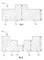
- FIG. 2is a schematic cross-sectional side view of a multiple thickness target in accordance with an embodiment of the present invention
- FIG. 3is a schematic cross-sectional side view of a multiple thickness target in accordance with an embodiment of the present invention.
- FIG. 4is a schematic cross-sectional side view of a multiple thickness target in accordance with an embodiment of the present invention.
- FIG. 5is a schematic top view of a multiple thickness target in accordance with an embodiment of the present invention.
- FIG. 6is a schematic cross-sectional side view of the multiple thickness target of FIG. 5 taken along line 6 - 6 in FIG. 5 ;
- FIG. 7is a schematic cross-sectional side view of a multiple thickness target in accordance with an embodiment of the present invention.
- FIG. 8is a schematic cross-sectional side view of a multiple thickness target in accordance with an embodiment of the present invention.
- FIG. 9is a schematic top view of a multiple thickness target in accordance with an embodiment of the present invention.
- FIG. 10is a schematic cross-sectional side view of the multiple thickness target of FIG. 9 taken along line 10 - 10 in FIG. 9 ;
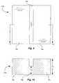
- FIG. 11is a schematic top view of a cathode filament in accordance with an embodiment of the present invention.
- FIG. 12is a schematic top view of a cathode filament in accordance with an embodiment of the present invention.
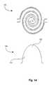
- FIG. 13is a schematic top view of a cathode filament and a laser beam intensity profile in accordance with an embodiment of the present invention
- FIG. 14is a schematic top view of a cathode filament and a laser beam intensity profile in accordance with an embodiment of the present invention.
- FIG. 15is a schematic cross-sectional side view of a multiple wavelength x-ray source in accordance with an embodiment of the present invention.
- FIG. 16is a schematic cross-sectional side view of a multiple wavelength x-ray source in accordance with an embodiment of the present invention.
- FIG. 17is a schematic cross-sectional side view of a multiple thickness target in accordance with an embodiment of the present invention.
- FIG. 18is a schematic cross-sectional side view of a multiple thickness target in accordance with an embodiment of the present invention.
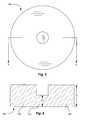
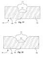
- the multiple wavelength x-ray source 10shown in FIG. 1 includes an evacuated tube 11 , an anode 12 coupled to the tube, and a cathode 16 , opposing the anode and also coupled to the tube 11 .
- the anode 12includes an x-ray transparent window 13 and a target 14 .
- FIG. 1shows the target 14 having a thickness that is similar to a thickness of the window 13 , typically the window 13 is much thicker than the target 14 .
- a relatively thicker target 14is shown in order to aid in showing features of the target, such as an inner region 15 a of the target and an outer region of the target 15 b , wherein one region is thicker than the other region, defining a thicker region and a thinner region.
- the cathode 16includes at least one electron source 17 which is configured to produce electrons accelerated towards the target 14 , in response to an electric field between the anode 12 and the cathode 16 , defining an electron beam.
- the electron source 17can be a filament.
- the target 14is comprised of a material configured to produce x-rays in response to impact of electrons.
- the multiple wavelength x-ray source 10also includes a means for expanding and narrowing an electron beam while maintaining a center or direction 18 of the electron beam in substantially the same location.
- an electron beam 21can be narrowed in order to impinge mostly upon the inner region 15 a of the target 14 .
- the electron beam 21can be expanded in order to impinge upon substantially the entire target region.
- the area of the outer regioncan be significantly greater than the area of the inner region such that when the electron beam 21 is expanded to impinge upon the entire target region, only a small fraction of the electron beam 21 will actually impinge upon the inner region.
- the electron beamcan be significantly stronger in the outer region or perimeter of the electron beam and significantly weaker in the central region of the electron beam such that only a very minimal portion of the electron beam will impinge on the inner region 15 a of the target when the electron beam is expanded.
- the outer region 15 bcan substantially circumscribe the inner region 15 a .
- both the outer region and the inner region shownare circular in shape, the target can also be other shapes, such as oval, square, rectangular, triangle, polygonal, etc.
- the inner regioncan have a thickness T 1 that is different from a thickness T 2 of the outer region.
- the inner regioncan be thinner and the outer region can be thicker.
- the target 14 bcan have the inner region be thicker and the outer region be thinner.
- a target 14 ccan have more than two thicknesses.
- a targetmay include more than the three different thicknesses shown in FIG. 8 .
- a target with more than two thicknessescan allow target thickness to be optimized at more than two tube voltages.
- the inner region 15 a of target 14 dshown in FIGS. 9 and 10 is in the shape of a channel.
- the thicker region 15 bis disposed on both sides of the inner region 15 a but does not necessarily circumscribe the inner region.
- the electron beamcan be narrowed to impinge primarily on the inner region 15 a and expanded to impinge mostly on the outer region 15 b of the target.
- the inner region 15 a of target 14 dis thinner than the outer region 15 b
- the opposite configurationmay be used in which the inner region 15 a is thicker than the outer region 15 b .
- Target 14 dmay be beneficial if the region where the electron beam impinges on the target is more linear in shape rather than circular.
- the electron beamcan be narrowed to impinge primarily upon the inner region 15 a when a lower voltage is applied between the anode 12 and the cathode 16 .
- the thickness T 1 of the inner region 15 a of the target 14can be optimized for this lower voltage. This can result in a strong L-line x-ray output.
- the electron beamcan be expanded to impinge primarily upon the outer and thicker region 15 b when a higher voltage is applied between the anode 12 and the cathode 16 .
- the thickness T 2 of the outer region 15 b of the target 14can be optimized for this higher voltage. This can result in a strong K-line x-ray output.
- the electron beamcan be narrowed to impinge primarily upon the inner region 15 a when a higher voltage is applied between the anode 12 and the cathode 16 .
- the thickness T 1 of the inner region 15 a of the target 14can be optimized for this higher voltage. This can result in a strong K-line x-ray output.
- the electron beamcan be expanded to impinge primarily upon the outer and thinner region 15 b when a lower voltage is applied between the anode 12 and the cathode 16 .
- the thickness T 2 of the outer region 15 b of the target 14can be optimized for this lower voltage. This can result in a strong L-line x-ray output.
- the means for expanding and narrowing the electron beamcan be a magnet 20 as shown in FIG. 1 .
- the magnet 20can be a permanent magnet.
- the permanent magnetcan cause the electron beam 21 to narrow when the permanent magnet is in close proximity to the anode.
- the electron beam 21can expand when the permanent magnet is moved away from the anode.
- the magnet 20can be an electromagnet.
- the electromagnetcan be annular and can surround the anode. For example, see U.S. Pat. No. 7,428,298 which is incorporated herein by reference.
- the electromagnetcan include additional electron beam optics for further shaping the electron beam.
- the electrical current through the electromagnetcan be adjusted, or turned on or off, to cause the electron beam to narrow or expand.
- the means for expanding and narrowing the electron beam, and the electron source 17can be at least one cathode filament.
- the filamentcan be resistively heated or laser heated.
- both filaments 110 of FIG. 11 and filament 120 of FIG. 12can be used.
- Filament 110includes an outer region 111 and an empty inner region 112 . Due to the shape of the filament 110 , an electron beam emitted from this filament can impinge primarily on an outer portion of the target. Although filament 110 is circular in shape, this filament could be other shapes depending on the shape of the outer region 15 b of the target 14 .
- Filament 120 (of FIG. 12 )can be placed in the empty inner region 112 of filament 110 (of FIG. 11 ). Filament 120 ( FIG. 12 ) can emit an electron beam that is narrow and stronger in the center.
- an electrical currentcan be passed through filament 120 when a lower voltage is applied between the cathode 15 and the anode 12 , thus causing a narrow electron beam to impinge primarily on the inner, thinner portion 15 a of the target 14 a .
- An electrical currentcan be passed through filament 110 when a higher voltage is applied between the cathode 15 and the anode 12 , thus causing a wider electron beam to impinge primarily on the outer, thicker portion 15 b of the target 14 a.
- a laser 19shown in FIG. 1 , can be used to selectively heat sections of a filament, such that the emitted electron beam can be more intense in the center or on the edges, corresponding to the desired section of the target.
- the laser 19 in FIG. 1is an optional addition to the embodiment shown in FIG. 1 .
- the electron source 17 in FIG. 1can be a filament which may be resistively heated rather than laser heated. Laser heated cathodes are described in U.S. Pat. No. 7,236,568, which is incorporated herein by reference.
- the filamentcan be a planar filament. Planar filaments are described in U.S. patent application Ser. No. 12/407,457, which is incorporated herein by reference. For example, filament 120 is shown in FIG.
- the laser beam profile 130is most intense at an outer perimeter 131 of the laser beam and less intense at a center of the laser beam 132 . This can result in a more intense laser beam heating the outer perimeter of the filament, causing an electron beam profile to be emitted from the filament 120 that is similar in shape to the laser beam profile—stronger at an outer perimeter and less intense at the center, thus the electron beam would impinge primarily upon outer region 15 b of the target and less upon the center 15 a of the target.
- the laser beamcan be more intense in the center 132 and less intense at the outer perimeter 131 as shown in laser beam intensity profile 140 of FIG. 14 .
- Thiscan result in a more intense laser beam heating the inner region of the filament 120 , causing an electron beam profile to be emitted from the filament 120 that is similar in shape to the laser beam profile—stronger at the center and less intense at the outer perimeter, thus the electron beam would impinge primarily upon an inner region 15 a of the anode target and less upon the outer region 15 b of the anode target.
- the means for expanding and narrowing the electron beamcan be electron beam optics combined with changes in tube voltage.
- the electron beam opticscan be designed so that the electron beam will be narrow when a lower voltage is applied across the tube and the electron beam expands when a higher voltage is applied across the tube.
- the electron beam opticscan be designed so that the electron beam will be narrow when a higher voltage is applied across the tube and the electron beam expands when a lower voltage is applied across the tube.
- cathode optics 151can cause the electron beam 21 to be narrow upon application of one voltage applied between the anode 12 and the cathode 16 and to expand upon application of a different voltage applied between the anode 12 and the cathode 16 .
- Targets 14 e and 14 fshown in FIGS. 17 and 18 , have gradual transitions 171 between the thicker and thinner regions. All invention embodiments can have either abrupt or gradual transitions in target thickness.
- a standard target for an x-ray tubemay be patterned and etched to create at least one thinner region.
- the targetcan be made of standard x-ray tube target materials, such as rhodium, tungsten, molybdenum, gold, silver, or copper, that can emit x-rays in response to an impinging electron beam.
- the target materialcan be selected such that the L and/or K lines of the target have a higher energy, and relatively close in energy, to a K-line or an L-line in the sample.
- the targetcan be made of a single material.
- U.S. patent application Ser. No. 12/603,242describes creating various shaped cavities by various patterning and etch procedures. Such procedures may be applicable in creating various shaped targets.
- U.S. patent application Ser. No. 12/603,242is incorporated herein by reference.
Landscapes
- X-Ray Techniques (AREA)
Abstract
Description
Claims (21)
Priority Applications (2)
| Application Number | Priority Date | Filing Date | Title |
|---|---|---|---|
| US12/640,154US7983394B2 (en) | 2009-12-17 | 2009-12-17 | Multiple wavelength X-ray source |
| PCT/US2010/056011WO2011084232A2 (en) | 2009-12-17 | 2010-11-09 | Multiple wavelength x-ray source |
Applications Claiming Priority (1)
| Application Number | Priority Date | Filing Date | Title |
|---|---|---|---|
| US12/640,154US7983394B2 (en) | 2009-12-17 | 2009-12-17 | Multiple wavelength X-ray source |
Publications (2)
| Publication Number | Publication Date |
|---|---|
| US20110150184A1 US20110150184A1 (en) | 2011-06-23 |
| US7983394B2true US7983394B2 (en) | 2011-07-19 |
Family
ID=44151120
Family Applications (1)
| Application Number | Title | Priority Date | Filing Date |
|---|---|---|---|
| US12/640,154Expired - Fee RelatedUS7983394B2 (en) | 2009-12-17 | 2009-12-17 | Multiple wavelength X-ray source |
Country Status (2)
| Country | Link |
|---|---|
| US (1) | US7983394B2 (en) |
| WO (1) | WO2011084232A2 (en) |
Cited By (18)
| Publication number | Priority date | Publication date | Assignee | Title |
|---|---|---|---|---|
| US20110280377A1 (en)* | 2010-05-11 | 2011-11-17 | Joerg Freudenberger | Thermionic surface emitter and associated method to operate an x-ray tube |
| US8247971B1 (en) | 2009-03-19 | 2012-08-21 | Moxtek, Inc. | Resistively heated small planar filament |
| US20120269324A1 (en)* | 2011-04-21 | 2012-10-25 | Adler David L | X-ray source with selective beam repositioning |
| US8406378B2 (en) | 2010-08-25 | 2013-03-26 | Gamc Biotech Development Co., Ltd. | Thick targets for transmission x-ray tubes |
| US8761344B2 (en) | 2011-12-29 | 2014-06-24 | Moxtek, Inc. | Small x-ray tube with electron beam control optics |
| US8948345B2 (en) | 2010-09-24 | 2015-02-03 | Moxtek, Inc. | X-ray tube high voltage sensing resistor |
| US9072154B2 (en) | 2012-12-21 | 2015-06-30 | Moxtek, Inc. | Grid voltage generation for x-ray tube |
| US9076628B2 (en) | 2011-05-16 | 2015-07-07 | Brigham Young University | Variable radius taper x-ray window support structure |
| US9177755B2 (en) | 2013-03-04 | 2015-11-03 | Moxtek, Inc. | Multi-target X-ray tube with stationary electron beam position |
| US9173623B2 (en) | 2013-04-19 | 2015-11-03 | Samuel Soonho Lee | X-ray tube and receiver inside mouth |
| US9174412B2 (en) | 2011-05-16 | 2015-11-03 | Brigham Young University | High strength carbon fiber composite wafers for microfabrication |
| US9184020B2 (en) | 2013-03-04 | 2015-11-10 | Moxtek, Inc. | Tiltable or deflectable anode x-ray tube |
| US9666322B2 (en) | 2014-02-23 | 2017-05-30 | Bruker Jv Israel Ltd | X-ray source assembly |
| US9748070B1 (en)* | 2014-09-17 | 2017-08-29 | Bruker Jv Israel Ltd. | X-ray tube anode |
| CN113707518A (en)* | 2021-08-20 | 2021-11-26 | 中国科学院电工研究所 | X-ray target |
| US11302508B2 (en) | 2018-11-08 | 2022-04-12 | Bruker Technologies Ltd. | X-ray tube |
| US20220399196A1 (en)* | 2019-11-11 | 2022-12-15 | Ametek Finland Oy | A shield device for a radiation window, a radiation arrangement comprising the shield device, and a method for producing the shield device |
| US11823860B1 (en)* | 2022-03-31 | 2023-11-21 | Canon Anelva Corporation | X-ray generating apparatus, method of adjusting target, and method of using X-ray generating apparatus |
Families Citing this family (8)
| Publication number | Priority date | Publication date | Assignee | Title |
|---|---|---|---|---|
| WO2014044316A1 (en)* | 2012-09-21 | 2014-03-27 | Siemens Aktiengesellschaft | Device having an anode for generating x-radiation |
| WO2014133797A1 (en)* | 2013-02-14 | 2014-09-04 | Golden Phillip | X-ray tube |
| JP6685670B2 (en)* | 2015-08-31 | 2020-04-22 | キヤノン株式会社 | X-ray generation tube, X-ray generation device, X-ray imaging system, and X-ray generation device adjustment method |
| JP6918595B2 (en)* | 2017-06-22 | 2021-08-11 | キヤノン電子管デバイス株式会社 | Fixed anode type X-ray tube |
| CN109211101B (en)* | 2018-10-11 | 2023-09-22 | 中国科学院电工研究所 | Electron beam centering detection tube and electron beam centering detection device |
| CN112912987B (en) | 2018-10-22 | 2022-05-31 | 佳能安内华股份有限公司 | X-ray generator and X-ray imaging system |
| US20220230833A1 (en)* | 2021-01-20 | 2022-07-21 | Moxtek, Inc. | Target Features to Increase X-Ray Flux |
| JP7665449B2 (en)* | 2021-06-30 | 2025-04-21 | 浜松ホトニクス株式会社 | X-ray generator |
Citations (219)
| Publication number | Priority date | Publication date | Assignee | Title |
|---|---|---|---|---|
| US1276706A (en) | 1918-04-30 | 1918-08-27 | Gurdy L Aydelotte | Land-torpedo. |
| US1881448A (en) | 1928-08-15 | 1932-10-11 | Formell Corp Ltd | X-ray method and means |
| US1946288A (en) | 1929-09-19 | 1934-02-06 | Gen Electric | Electron discharge device |
| US2291948A (en) | 1940-06-27 | 1942-08-04 | Westinghouse Electric & Mfg Co | High voltage X-ray tube shield |
| US2316214A (en) | 1940-09-10 | 1943-04-13 | Gen Electric X Ray Corp | Control of electron flow |
| US2329318A (en) | 1941-09-08 | 1943-09-14 | Gen Electric X Ray Corp | X-ray generator |
| US2340363A (en) | 1942-03-03 | 1944-02-01 | Gen Electric X Ray Corp | Control for focal spot in X-ray generators |
| US2502070A (en) | 1949-01-19 | 1950-03-28 | Dunlee Corp | Getter for induction flashing |
| US2683223A (en) | 1952-07-24 | 1954-07-06 | Licentia Gmbh | X-ray tube |
| DE1030936B (en) | 1952-01-11 | 1958-05-29 | Licentia Gmbh | Vacuum-tight radiation window made of beryllium for discharge vessels |
| US2952790A (en) | 1957-07-15 | 1960-09-13 | Raytheon Co | X-ray tubes |
| US3218559A (en) | 1961-11-09 | 1965-11-16 | Gen Electric | Synchronizing circuit maintaining loop signals as an integer product and equal amplitude |
| US3356559A (en) | 1963-07-01 | 1967-12-05 | University Patents Inc | Colored fiber metal structures and method of making the same |
| US3397337A (en) | 1966-01-14 | 1968-08-13 | Ion Physics Corp | Flash X-ray dielectric wall structure |
| US3434062A (en) | 1965-06-21 | 1969-03-18 | James R Cox | Drift detector |
| US3538368A (en) | 1968-01-02 | 1970-11-03 | Hughes Aircraft Co | Electron gun structure employing a unitary cylinder housing |
| GB1252290A (en) | 1967-12-28 | 1971-11-03 | ||
| US3665236A (en) | 1970-12-09 | 1972-05-23 | Atomic Energy Commission | Electrode structure for controlling electron flow with high transmission efficiency |
| US3679927A (en) | 1970-08-17 | 1972-07-25 | Machlett Lab Inc | High power x-ray tube |
| US3691417A (en) | 1969-09-02 | 1972-09-12 | Watkins Johnson Co | X-ray generating assembly and system |
| US3741797A (en) | 1970-04-30 | 1973-06-26 | Gen Technology Corp | Low density high-strength boron on beryllium reinforcement filaments |
| US3751701A (en) | 1971-03-08 | 1973-08-07 | Watkins Johnson Co | Convergent flow hollow beam x-ray gun with high average power |
| US3801847A (en)* | 1971-11-04 | 1974-04-02 | Siemens Ag | X-ray tube |
| US3828190A (en) | 1969-01-17 | 1974-08-06 | Measurex Corp | Detector assembly |
| US3851266A (en) | 1967-07-27 | 1974-11-26 | P Conway | Signal conditioner and bit synchronizer |
| US3872287A (en) | 1971-07-30 | 1975-03-18 | Philips Corp | Method of, and apparatus for, determining radiation energy distributions |
| US3882339A (en)* | 1974-06-17 | 1975-05-06 | Gen Electric | Gridded X-ray tube gun |
| US3894219A (en) | 1974-01-16 | 1975-07-08 | Westinghouse Electric Corp | Hybrid analog and digital comb filter for clutter cancellation |
| US3962583A (en) | 1974-12-30 | 1976-06-08 | The Machlett Laboratories, Incorporated | X-ray tube focusing means |
| US3970884A (en) | 1973-07-09 | 1976-07-20 | Golden John P | Portable X-ray device |
| US4007375A (en) | 1975-07-14 | 1977-02-08 | Albert Richard D | Multi-target X-ray source |
| US4075526A (en)* | 1975-11-28 | 1978-02-21 | Compagnie Generale De Radiologie | Hot-cathode x-ray tube having an end-mounted anode |
| US4160311A (en) | 1976-01-16 | 1979-07-10 | U.S. Philips Corporation | Method of manufacturing a cathode ray tube for displaying colored pictures |
| US4178509A (en) | 1978-06-02 | 1979-12-11 | The Bendix Corporation | Sensitivity proportional counter window |
| US4184097A (en) | 1977-02-25 | 1980-01-15 | Magnaflux Corporation | Internally shielded X-ray tube |
| US4293373A (en) | 1978-05-30 | 1981-10-06 | International Standard Electric Corporation | Method of making transducer |
| US4368538A (en) | 1980-04-11 | 1983-01-11 | International Business Machines Corporation | Spot focus flash X-ray source |
| US4393127A (en) | 1980-09-19 | 1983-07-12 | International Business Machines Corporation | Structure with a silicon body having through openings |
| US4421986A (en) | 1980-11-21 | 1983-12-20 | The United States Of America As Represented By The Department Of Health And Human Services | Nuclear pulse discriminator |
| US4443293A (en) | 1981-04-20 | 1984-04-17 | Kulite Semiconductor Products, Inc. | Method of fabricating transducer structure employing vertically walled diaphragms with quasi rectangular active areas |
| US4463338A (en) | 1980-08-28 | 1984-07-31 | Siemens Aktiengesellschaft | Electrical network and method for producing the same |
| US4521902A (en) | 1983-07-05 | 1985-06-04 | Ridge, Inc. | Microfocus X-ray system |
| US4532150A (en) | 1982-12-29 | 1985-07-30 | Shin-Etsu Chemical Co., Ltd. | Method for providing a coating layer of silicon carbide on the surface of a substrate |
| US4573186A (en) | 1982-06-16 | 1986-02-25 | Feinfocus Rontgensysteme Gmbh | Fine focus X-ray tube and method of forming a microfocus of the electron emission of an X-ray tube hot cathode |
| US4576679A (en) | 1981-03-27 | 1986-03-18 | Honeywell Inc. | Method of fabricating a cold shield |
| US4584056A (en) | 1983-11-18 | 1986-04-22 | Centre Electronique Horloger S.A. | Method of manufacturing a device with micro-shutters and application of such a method to obtain a light modulating device |
| US4591756A (en) | 1985-02-25 | 1986-05-27 | Energy Sciences, Inc. | High power window and support structure for electron beam processors |
| US4608326A (en) | 1984-02-13 | 1986-08-26 | Hewlett-Packard Company | Silicon carbide film for X-ray masks and vacuum windows |
| US4645977A (en) | 1984-08-31 | 1987-02-24 | Matsushita Electric Industrial Co., Ltd. | Plasma CVD apparatus and method for forming a diamond like carbon film |
| US4675525A (en) | 1985-02-06 | 1987-06-23 | Commissariat A L'energie Atomique | Matrix device for the detection of light radiation with individual cold screens integrated into a substrate and its production process |
| US4679219A (en) | 1984-06-15 | 1987-07-07 | Kabushiki Kaisha Toshiba | X-ray tube |
| US4688241A (en)* | 1984-03-26 | 1987-08-18 | Ridge, Inc. | Microfocus X-ray system |
| US4696994A (en) | 1984-12-14 | 1987-09-29 | Ube Industries, Ltd. | Transparent aromatic polyimide |
| US4705540A (en) | 1986-04-17 | 1987-11-10 | E. I. Du Pont De Nemours And Company | Polyimide gas separation membranes |
| US4777642A (en) | 1985-07-24 | 1988-10-11 | Kabushiki Kaisha Toshiba | X-ray tube device |
| US4797907A (en) | 1987-08-07 | 1989-01-10 | Diasonics Inc. | Battery enhanced power generation for mobile X-ray machine |
| US4818806A (en) | 1985-05-31 | 1989-04-04 | Chisso Corporation | Process for producing highly adherent silicon-containing polyamic acid and corsslinked silicon-containing polyimide |
| US4819260A (en) | 1985-11-28 | 1989-04-04 | Siemens Aktiengesellschaft | X-radiator with non-migrating focal spot |
| US4862490A (en) | 1986-10-23 | 1989-08-29 | Hewlett-Packard Company | Vacuum windows for soft x-ray machines |
| US4870671A (en) | 1988-10-25 | 1989-09-26 | X-Ray Technologies, Inc. | Multitarget x-ray tube |
| US4876330A (en) | 1985-03-10 | 1989-10-24 | Nitto Electric Industrial Co., Ltd. | Colorless transparent polyimide shaped article and process for producing the same |
| US4878866A (en) | 1986-07-14 | 1989-11-07 | Denki Kagaku Kogyo Kabushiki Kaisha | Thermionic cathode structure |
| US4885055A (en) | 1987-08-21 | 1989-12-05 | Brigham Young University | Layered devices having surface curvature and method of constructing same |
| US4933557A (en) | 1988-06-06 | 1990-06-12 | Brigham Young University | Radiation detector window structure and method of manufacturing thereof |
| US4939763A (en) | 1988-10-03 | 1990-07-03 | Crystallume | Method for preparing diamond X-ray transmissive elements |
| US4957773A (en) | 1989-02-13 | 1990-09-18 | Syracuse University | Deposition of boron-containing films from decaborane |
| US4960486A (en) | 1988-06-06 | 1990-10-02 | Brigham Young University | Method of manufacturing radiation detector window structure |
| US4969173A (en)* | 1986-12-23 | 1990-11-06 | U.S. Philips Corporation | X-ray tube comprising an annular focus |
| US4979199A (en) | 1989-10-31 | 1990-12-18 | General Electric Company | Microfocus X-ray tube with optical spot size sensing means |
| US4979198A (en) | 1986-05-15 | 1990-12-18 | Malcolm David H | Method for production of fluoroscopic and radiographic x-ray images and hand held diagnostic apparatus incorporating the same |
| US5010562A (en) | 1989-08-31 | 1991-04-23 | Siemens Medical Laboratories, Inc. | Apparatus and method for inhibiting the generation of excessive radiation |
| US5063324A (en) | 1990-03-29 | 1991-11-05 | Itt Corporation | Dispenser cathode with emitting surface parallel to ion flow |
| US5066300A (en) | 1988-05-02 | 1991-11-19 | Nu-Tech Industries, Inc. | Twin replacement heart |
| EP0297808B1 (en) | 1987-07-02 | 1991-12-11 | MITSUI TOATSU CHEMICALS, Inc. | Polyimide and high-temperature adhesive thereof |
| US5077771A (en) | 1989-03-01 | 1991-12-31 | Kevex X-Ray Inc. | Hand held high power pulsed precision x-ray source |
| US5077777A (en) | 1990-07-02 | 1991-12-31 | Micro Focus Imaging Corp. | Microfocus X-ray tube |
| US5105456A (en) | 1988-11-23 | 1992-04-14 | Imatron, Inc. | High duty-cycle x-ray tube |
| US5117829A (en) | 1989-03-31 | 1992-06-02 | Loma Linda University Medical Center | Patient alignment system and procedure for radiation treatment |
| US5153900A (en) | 1990-09-05 | 1992-10-06 | Photoelectron Corporation | Miniaturized low power x-ray source |
| US5161179A (en) | 1990-03-01 | 1992-11-03 | Yamaha Corporation | Beryllium window incorporated in X-ray radiation system and process of fabrication thereof |
| US5173612A (en) | 1990-09-18 | 1992-12-22 | Sumitomo Electric Industries Ltd. | X-ray window and method of producing same |
| US5178140A (en) | 1991-09-05 | 1993-01-12 | Telectronics Pacing Systems, Inc. | Implantable medical devices employing capacitive control of high voltage switches |
| US5217817A (en) | 1989-11-08 | 1993-06-08 | U.S. Philips Corporation | Steel tool provided with a boron layer |
| US5226067A (en) | 1992-03-06 | 1993-07-06 | Brigham Young University | Coating for preventing corrosion to beryllium x-ray windows and method of preparing |
| USRE34421E (en) | 1990-11-21 | 1993-10-26 | Parker William J | X-ray micro-tube and method of use in radiation oncology |
| US5258091A (en) | 1990-09-18 | 1993-11-02 | Sumitomo Electric Industries, Ltd. | Method of producing X-ray window |
| US5267294A (en) | 1992-04-22 | 1993-11-30 | Hitachi Medical Corporation | Radiotherapy apparatus |
| US5302523A (en) | 1989-06-21 | 1994-04-12 | Zeneca Limited | Transformation of plant cells |
| US5343112A (en) | 1989-01-18 | 1994-08-30 | Balzers Aktiengesellschaft | Cathode arrangement |
| EP0330456B1 (en) | 1988-02-26 | 1994-09-07 | Chisso Corporation | Preparation of silicon-containing polyimide precursor and cured polyimides obtained therefrom |
| US5391958A (en) | 1993-04-12 | 1995-02-21 | Charged Injection Corporation | Electron beam window devices and methods of making same |
| US5392042A (en) | 1993-08-05 | 1995-02-21 | Martin Marietta Corporation | Sigma-delta analog-to-digital converter with filtration having controlled pole-zero locations, and apparatus therefor |
| US5400385A (en) | 1993-09-02 | 1995-03-21 | General Electric Company | High voltage power supply for an X-ray tube |
| US5428658A (en) | 1994-01-21 | 1995-06-27 | Photoelectron Corporation | X-ray source with flexible probe |
| US5432003A (en) | 1988-10-03 | 1995-07-11 | Crystallume | Continuous thin diamond film and method for making same |
| US5469429A (en) | 1993-05-21 | 1995-11-21 | Kabushiki Kaisha Toshiba | X-ray CT apparatus having focal spot position detection means for the X-ray tube and focal spot position adjusting means |
| US5469490A (en) | 1993-10-26 | 1995-11-21 | Golden; John | Cold-cathode X-ray emitter and tube therefor |
| US5478266A (en) | 1993-04-12 | 1995-12-26 | Charged Injection Corporation | Beam window devices and methods of making same |
| US5521851A (en) | 1993-04-26 | 1996-05-28 | Nihon Kohden Corporation | Noise reduction method and apparatus |
| US5524133A (en) | 1992-01-15 | 1996-06-04 | Cambridge Imaging Limited | Material identification using x-rays |
| US5571616A (en) | 1995-05-16 | 1996-11-05 | Crystallume | Ultrasmooth adherent diamond film coated article and method for making same |
| USRE35383E (en) | 1992-03-23 | 1996-11-26 | The Titan Corporation | Interstitial X-ray needle |
| US5578360A (en) | 1992-05-07 | 1996-11-26 | Outokumpu Instruments Oy | Thin film reinforcing structure and method for manufacturing the same |
| US5602507A (en) | 1993-11-05 | 1997-02-11 | Ntt Mobile Communications Network Inc. | Adaptive demodulating method for generating replica and demodulator thereof |
| US5607723A (en) | 1988-10-21 | 1997-03-04 | Crystallume | Method for making continuous thin diamond film |
| US5621780A (en) | 1990-09-05 | 1997-04-15 | Photoelectron Corporation | X-ray apparatus for applying a predetermined flux to an interior surface of a body cavity |
| US5627871A (en)* | 1993-06-10 | 1997-05-06 | Nanodynamics, Inc. | X-ray tube and microelectronics alignment process |
| US5631943A (en) | 1995-12-19 | 1997-05-20 | Miles; Dale A. | Portable X-ray device |
| US5680433A (en)* | 1995-04-28 | 1997-10-21 | Varian Associates, Inc. | High output stationary X-ray target with flexible support structure |
| US5682412A (en) | 1993-04-05 | 1997-10-28 | Cardiac Mariners, Incorporated | X-ray source |
| US5696808A (en) | 1995-09-28 | 1997-12-09 | Siemens Aktiengesellschaft | X-ray tube |
| US5729583A (en) | 1995-09-29 | 1998-03-17 | The United States Of America As Represented By The Secretary Of Commerce | Miniature x-ray source |
| US5774522A (en) | 1995-08-14 | 1998-06-30 | Warburton; William K. | Method and apparatus for digitally based high speed x-ray spectrometer for direct coupled use with continuous discharge preamplifiers |
| DE4430623C2 (en) | 1994-08-29 | 1998-07-02 | Siemens Ag | X-ray image intensifier |
| US5812632A (en) | 1996-09-27 | 1998-09-22 | Siemens Aktiengesellschaft | X-ray tube with variable focus |
| US5835561A (en) | 1993-01-25 | 1998-11-10 | Cardiac Mariners, Incorporated | Scanning beam x-ray imaging system |
| US5870051A (en) | 1995-08-14 | 1999-02-09 | William K. Warburton | Method and apparatus for analog signal conditioner for high speed, digital x-ray spectrometer |
| US5898754A (en) | 1997-06-13 | 1999-04-27 | X-Ray And Specialty Instruments, Inc. | Method and apparatus for making a demountable x-ray tube |
| US5907595A (en) | 1997-08-18 | 1999-05-25 | General Electric Company | Emitter-cup cathode for high-emission x-ray tube |
| DE19818057A1 (en) | 1998-04-22 | 1999-11-04 | Siemens Ag | X-ray image intensifier manufacture method |
| US6002202A (en) | 1996-07-19 | 1999-12-14 | The Regents Of The University Of California | Rigid thin windows for vacuum applications |
| US6005918A (en) | 1997-12-19 | 1999-12-21 | Picker International, Inc. | X-ray tube window heat shield |
| US6044130A (en) | 1995-12-25 | 2000-03-28 | Hamamatsu Photonics K.K. | Transmission type X-ray tube |
| US6062931A (en) | 1999-09-01 | 2000-05-16 | Industrial Technology Research Institute | Carbon nanotube emitter with triode structure |
| US6063629A (en) | 1998-06-05 | 2000-05-16 | Wolfgang Lummel | Microinjection process for introducing an injection substance particularly foreign, genetic material, into procaryotic and eucaryotic cells, as well as cell compartments of the latter (plastids, cell nuclei), as well as nanopipette for the same |
| US6069278A (en) | 1998-01-23 | 2000-05-30 | The United States Of America As Represented By The Administrator Of The National Aeronautics And Space Administration | Aromatic diamines and polyimides based on 4,4'-bis-(4-aminophenoxy)-2,2' or 2,2',6,6'-substituted biphenyl |
| US6075839A (en) | 1997-09-02 | 2000-06-13 | Varian Medical Systems, Inc. | Air cooled end-window metal-ceramic X-ray tube for lower power XRF applications |
| US6097790A (en) | 1997-02-26 | 2000-08-01 | Canon Kabushiki Kaisha | Pressure partition for X-ray exposure apparatus |
| US6129901A (en) | 1997-11-18 | 2000-10-10 | Martin Moskovits | Controlled synthesis and metal-filling of aligned carbon nanotubes |
| US6133401A (en) | 1998-06-29 | 2000-10-17 | The United States Of America As Represented By The Administrator Of The National Aeronautics And Space Administration | Method to prepare processable polyimides with reactive endgroups using 1,3-bis (3-aminophenoxy) benzene |
| US6134300A (en) | 1998-11-05 | 2000-10-17 | The Regents Of The University Of California | Miniature x-ray source |
| US6184333B1 (en) | 1998-01-16 | 2001-02-06 | Maverick Corporation | Low-toxicity, high-temperature polyimides |
| US6205200B1 (en) | 1996-10-28 | 2001-03-20 | The United States Of America As Represented By The Secretary Of The Navy | Mobile X-ray unit |
| JP3170673B2 (en) | 1994-11-15 | 2001-05-28 | 株式会社テイエルブイ | Liquid pumping device |
| US6277318B1 (en) | 1999-08-18 | 2001-08-21 | Agere Systems Guardian Corp. | Method for fabrication of patterned carbon nanotube films |
| US6282263B1 (en) | 1996-09-27 | 2001-08-28 | Bede Scientific Instruments Limited | X-ray generator |
| US6307008B1 (en) | 2000-02-25 | 2001-10-23 | Saehan Industries Corporation | Polyimide for high temperature adhesive |
| US6320019B1 (en) | 2000-02-22 | 2001-11-20 | Saehan Industries Incorporation | Method for the preparation of polyamic acid and polyimide |
| US6351520B1 (en) | 1997-12-04 | 2002-02-26 | Hamamatsu Photonics K.K. | X-ray tube |
| US6385294B2 (en) | 1998-07-30 | 2002-05-07 | Hamamatsu Photonics K.K. | X-ray tube |
| US6388359B1 (en) | 2000-03-03 | 2002-05-14 | Optical Coating Laboratory, Inc. | Method of actuating MEMS switches |
| US20020075999A1 (en) | 2000-09-29 | 2002-06-20 | Peter Rother | Vacuum enclosure for a vacuum tube tube having an X-ray window |
| US20020094064A1 (en) | 2000-10-06 | 2002-07-18 | Zhou Otto Z. | Large-area individually addressable multi-beam x-ray system and method of forming same |
| US6438207B1 (en) | 1999-09-14 | 2002-08-20 | Varian Medical Systems, Inc. | X-ray tube having improved focal spot control |
| US6477235B2 (en) | 1999-03-23 | 2002-11-05 | Victor Ivan Chornenky | X-Ray device and deposition process for manufacture |
| US6487273B1 (en) | 1999-11-26 | 2002-11-26 | Varian Medical Systems, Inc. | X-ray tube having an integral housing assembly |
| US6487272B1 (en)* | 1999-02-19 | 2002-11-26 | Kabushiki Kaisha Toshiba | Penetrating type X-ray tube and manufacturing method thereof |
| US6494618B1 (en) | 2000-08-15 | 2002-12-17 | Varian Medical Systems, Inc. | High voltage receptacle for x-ray tubes |
| US6546077B2 (en) | 2001-01-17 | 2003-04-08 | Medtronic Ave, Inc. | Miniature X-ray device and method of its manufacture |
| JP2003211396A (en) | 2002-01-21 | 2003-07-29 | Ricoh Co Ltd | Micro machine |
| US20030152700A1 (en) | 2002-02-11 | 2003-08-14 | Board Of Trustees Operating Michigan State University | Process for synthesizing uniform nanocrystalline films |
| US20030165418A1 (en) | 2002-02-11 | 2003-09-04 | Rensselaer Polytechnic Institute | Directed assembly of highly-organized carbon nanotube architectures |
| US6646366B2 (en) | 2001-07-24 | 2003-11-11 | Siemens Aktiengesellschaft | Directly heated thermionic flat emitter |
| US6645757B1 (en) | 2001-02-08 | 2003-11-11 | Sandia Corporation | Apparatus and method for transforming living cells |
| US6658085B2 (en) | 2000-08-04 | 2003-12-02 | Siemens Aktiengesellschaft | Medical examination installation with an MR system and an X-ray system |
| US6661876B2 (en) | 2001-07-30 | 2003-12-09 | Moxtek, Inc. | Mobile miniature X-ray source |
| US20040076260A1 (en)* | 2002-01-31 | 2004-04-22 | Charles Jr Harry K. | X-ray source and method for more efficiently producing selectable x-ray frequencies |
| US6740874B2 (en) | 2001-04-26 | 2004-05-25 | Bruker Saxonia Analytik Gmbh | Ion mobility spectrometer with mechanically stabilized vacuum-tight x-ray window |
| US6778633B1 (en) | 1999-03-26 | 2004-08-17 | Bede Scientific Instruments Limited | Method and apparatus for prolonging the life of an X-ray target |
| US6799075B1 (en) | 1995-08-24 | 2004-09-28 | Medtronic Ave, Inc. | X-ray catheter |
| US6803570B1 (en) | 2003-07-11 | 2004-10-12 | Charles E. Bryson, III | Electron transmissive window usable with high pressure electron spectrometry |
| US6816573B2 (en) | 1999-03-02 | 2004-11-09 | Hamamatsu Photonics K.K. | X-ray generating apparatus, X-ray imaging apparatus, and X-ray inspection system |
| US6819741B2 (en) | 2003-03-03 | 2004-11-16 | Varian Medical Systems Inc. | Apparatus and method for shaping high voltage potentials on an insulator |
| US6838297B2 (en) | 1998-03-27 | 2005-01-04 | Canon Kabushiki Kaisha | Nanostructure, electron emitting device, carbon nanotube device, and method of producing the same |
| US20050018817A1 (en) | 2002-02-20 | 2005-01-27 | Oettinger Peter E. | Integrated X-ray source module |
| US6852365B2 (en) | 2001-03-26 | 2005-02-08 | Kumetrix, Inc. | Silicon penetration device with increased fracture toughness and method of fabrication |
| US6866801B1 (en) | 1999-09-23 | 2005-03-15 | Commonwealth Scientific And Industrial Research Organisation | Process for making aligned carbon nanotubes |
| US6900580B2 (en) | 1998-11-12 | 2005-05-31 | The Board Of Trustees Of The Leland Stanford Junior University | Self-oriented bundles of carbon nanotubes and method of making same |
| US20050141669A1 (en) | 2003-01-10 | 2005-06-30 | Toshiba Electron Tube & Devices Co., Ltd | X-ray equipment |
| US20050207537A1 (en)* | 2002-07-19 | 2005-09-22 | Masaaki Ukita | X-ray generating equipment |
| US6956706B2 (en) | 2000-04-03 | 2005-10-18 | John Robert Brandon | Composite diamond window |
| US6962782B1 (en) | 1999-02-08 | 2005-11-08 | Commissariat A L'energie Atomique | Method for producing addressed ligands matrixes on a support |
| US6976953B1 (en) | 2000-03-30 | 2005-12-20 | The Board Of Trustees Of The Leland Stanford Junior University | Maintaining the alignment of electric and magnetic fields in an x-ray tube operated in a magnetic field |
| US6987835B2 (en) | 2003-03-26 | 2006-01-17 | Xoft Microtube, Inc. | Miniature x-ray tube with micro cathode |
| US20060073682A1 (en) | 2004-10-04 | 2006-04-06 | International Business Machines Corporation | Low-k dielectric material based upon carbon nanotubes and methods of forming such low-k dielectric materials |
| US7035379B2 (en) | 2002-09-13 | 2006-04-25 | Moxtek, Inc. | Radiation window and method of manufacture |
| US20060098778A1 (en) | 2002-02-20 | 2006-05-11 | Oettinger Peter E | Integrated X-ray source module |
| US7046767B2 (en) | 2001-05-31 | 2006-05-16 | Hamamatsu Photonics K.K. | X-ray generator |
| US7049735B2 (en) | 2004-01-07 | 2006-05-23 | Matsushita Electric Industrial Co., Ltd. | Incandescent bulb and incandescent bulb filament |
| US7075699B2 (en) | 2003-09-29 | 2006-07-11 | The Regents Of The University Of California | Double hidden flexure microactuator for phase mirror array |
| US7085354B2 (en) | 2003-01-21 | 2006-08-01 | Toshiba Electron Tube & Devices Co., Ltd. | X-ray tube apparatus |
| US7110498B2 (en) | 2003-09-12 | 2006-09-19 | Canon Kabushiki Kaisha | Image reading apparatus and X-ray imaging apparatus |
| US7108841B2 (en) | 1997-03-07 | 2006-09-19 | William Marsh Rice University | Method for forming a patterned array of single-wall carbon nanotubes |
| US20060233307A1 (en) | 2001-06-19 | 2006-10-19 | Mark Dinsmore | X-ray source for materials analysis systems |
| US7130380B2 (en) | 2004-03-13 | 2006-10-31 | Xoft, Inc. | Extractor cup on a miniature x-ray tube |
| JP2006297549A (en) | 2005-04-21 | 2006-11-02 | Keio Gijuku | Method of array deposition of metal nanoparticles and method of growing carbon nanotubes using metal nanoparticles |
| US20060269048A1 (en) | 2005-05-25 | 2006-11-30 | Cain Bruce A | Removable aperture cooling structure for an X-ray tube |
| US20070025516A1 (en)* | 2005-03-31 | 2007-02-01 | Bard Erik C | Magnetic head for X-ray source |
| US7203283B1 (en) | 2006-02-21 | 2007-04-10 | Oxford Instruments Analytical Oy | X-ray tube of the end window type, and an X-ray fluorescence analyzer |
| US20070087436A1 (en) | 2003-04-11 | 2007-04-19 | Atsushi Miyawaki | Microinjection method and device |
| US7215741B2 (en) | 2004-03-26 | 2007-05-08 | Shimadzu Corporation | X-ray generating apparatus |
| US20070111617A1 (en) | 2005-11-17 | 2007-05-17 | Oxford Instruments Analytical Oy | Window membrane for detector and analyser devices, and a method for manufacturing a window membrane |
| US20070107210A1 (en) | 2003-07-31 | 2007-05-17 | Karl Keller | Device for installing and removing a roller supporting a bearing assembly |
| US7224769B2 (en) | 2004-02-20 | 2007-05-29 | Aribex, Inc. | Digital x-ray camera |
| US20070133921A1 (en) | 2005-12-08 | 2007-06-14 | Haffner Ken Y | Optical Sensor Device for Local Analysis of a Combustion Process in a Combustor of a Thermal Power Plant |
| US20070142781A1 (en) | 2005-12-21 | 2007-06-21 | Sayre Chauncey B | Microinjector chip |
| US20070165780A1 (en) | 2006-01-19 | 2007-07-19 | Bruker Axs, Inc. | Multiple wavelength X-ray source |
| US20070183576A1 (en) | 2006-01-31 | 2007-08-09 | Burke James E | Cathode head having filament protection features |
| US7286642B2 (en) | 2002-04-05 | 2007-10-23 | Hamamatsu Photonics K.K. | X-ray tube control apparatus and x-ray tube control method |
| US7358593B2 (en) | 2004-05-07 | 2008-04-15 | University Of Maine | Microfabricated miniature grids |
| US7382862B2 (en) | 2005-09-30 | 2008-06-03 | Moxtek, Inc. | X-ray tube cathode with reduced unintended electrical field emission |
| US20080199399A1 (en) | 2007-02-21 | 2008-08-21 | Xing Chen | Interfacing Nanostructures to Biological Cells |
| JP4171700B2 (en) | 2001-11-21 | 2008-10-22 | ノバルティス アクチエンゲゼルシャフト | Heterocyclic compounds and methods of use |
| US20080296518A1 (en) | 2007-06-01 | 2008-12-04 | Degao Xu | X-Ray Window with Grid Structure |
| US20080296479A1 (en) | 2007-06-01 | 2008-12-04 | Anderson Eric C | Polymer X-Ray Window with Diamond Support Structure |
| US20080317982A1 (en) | 2006-10-13 | 2008-12-25 | Unidym, Inc. | Compliant and nonplanar nanostructure films |
| US20090085426A1 (en) | 2007-09-28 | 2009-04-02 | Davis Robert C | Carbon nanotube mems assembly |
| US20090086923A1 (en) | 2007-09-28 | 2009-04-02 | Davis Robert C | X-ray radiation window with carbon nanotube frame |
| US7529345B2 (en) | 2007-07-18 | 2009-05-05 | Moxtek, Inc. | Cathode header optic for x-ray tube |
| US20090213914A1 (en) | 2004-06-03 | 2009-08-27 | Silicon Laboratories Inc. | Capacitive isolation circuitry |
| US20090243028A1 (en) | 2004-06-03 | 2009-10-01 | Silicon Laboratories Inc. | Capacitive isolation circuitry with improved common mode detector |
| US7634052B2 (en) | 2006-10-24 | 2009-12-15 | Thermo Niton Analyzers Llc | Two-stage x-ray concentrator |
| US7649980B2 (en)* | 2006-12-04 | 2010-01-19 | The University Of Tokyo | X-ray source |
| US7675444B1 (en) | 2008-09-23 | 2010-03-09 | Maxim Integrated Products, Inc. | High voltage isolation by capacitive coupling |
| US7680652B2 (en) | 2004-10-26 | 2010-03-16 | Qnx Software Systems (Wavemakers), Inc. | Periodic signal enhancement system |
| US7693265B2 (en) | 2006-05-11 | 2010-04-06 | Koninklijke Philips Electronics N.V. | Emitter design including emergency operation mode in case of emitter-damage for medical X-ray application |
| US7709820B2 (en) | 2007-06-01 | 2010-05-04 | Moxtek, Inc. | Radiation window with coated silicon support structure |
| US20100239828A1 (en) | 2009-03-19 | 2010-09-23 | Cornaby Sterling W | Resistively heated small planar filament |
| US20100248343A1 (en) | 2007-07-09 | 2010-09-30 | Aten Quentin T | Methods and Devices for Charged Molecule Manipulation |
Family Cites Families (3)
| Publication number | Priority date | Publication date | Assignee | Title |
|---|---|---|---|---|
| JPH0787082B2 (en)* | 1987-07-24 | 1995-09-20 | 株式会社日立製作所 | Rotating anode target for X-ray tube |
| JP2886588B2 (en)* | 1989-07-11 | 1999-04-26 | 日本碍子株式会社 | Piezoelectric / electrostrictive actuator |
| JP2003007237A (en)* | 2001-06-25 | 2003-01-10 | Shimadzu Corp | X-ray generator |
- 2009
- 2009-12-17USUS12/640,154patent/US7983394B2/ennot_activeExpired - Fee Related
- 2010
- 2010-11-09WOPCT/US2010/056011patent/WO2011084232A2/enactiveApplication Filing
Patent Citations (241)
| Publication number | Priority date | Publication date | Assignee | Title |
|---|---|---|---|---|
| US1276706A (en) | 1918-04-30 | 1918-08-27 | Gurdy L Aydelotte | Land-torpedo. |
| US1881448A (en) | 1928-08-15 | 1932-10-11 | Formell Corp Ltd | X-ray method and means |
| US1946288A (en) | 1929-09-19 | 1934-02-06 | Gen Electric | Electron discharge device |
| US2291948A (en) | 1940-06-27 | 1942-08-04 | Westinghouse Electric & Mfg Co | High voltage X-ray tube shield |
| US2316214A (en) | 1940-09-10 | 1943-04-13 | Gen Electric X Ray Corp | Control of electron flow |
| US2329318A (en) | 1941-09-08 | 1943-09-14 | Gen Electric X Ray Corp | X-ray generator |
| US2340363A (en) | 1942-03-03 | 1944-02-01 | Gen Electric X Ray Corp | Control for focal spot in X-ray generators |
| US2502070A (en) | 1949-01-19 | 1950-03-28 | Dunlee Corp | Getter for induction flashing |
| DE1030936B (en) | 1952-01-11 | 1958-05-29 | Licentia Gmbh | Vacuum-tight radiation window made of beryllium for discharge vessels |
| US2683223A (en) | 1952-07-24 | 1954-07-06 | Licentia Gmbh | X-ray tube |
| US2952790A (en) | 1957-07-15 | 1960-09-13 | Raytheon Co | X-ray tubes |
| US3218559A (en) | 1961-11-09 | 1965-11-16 | Gen Electric | Synchronizing circuit maintaining loop signals as an integer product and equal amplitude |
| US3356559A (en) | 1963-07-01 | 1967-12-05 | University Patents Inc | Colored fiber metal structures and method of making the same |
| US3434062A (en) | 1965-06-21 | 1969-03-18 | James R Cox | Drift detector |
| US3397337A (en) | 1966-01-14 | 1968-08-13 | Ion Physics Corp | Flash X-ray dielectric wall structure |
| US3851266A (en) | 1967-07-27 | 1974-11-26 | P Conway | Signal conditioner and bit synchronizer |
| GB1252290A (en) | 1967-12-28 | 1971-11-03 | ||
| US3538368A (en) | 1968-01-02 | 1970-11-03 | Hughes Aircraft Co | Electron gun structure employing a unitary cylinder housing |
| US3828190A (en) | 1969-01-17 | 1974-08-06 | Measurex Corp | Detector assembly |
| US3691417A (en) | 1969-09-02 | 1972-09-12 | Watkins Johnson Co | X-ray generating assembly and system |
| US3741797A (en) | 1970-04-30 | 1973-06-26 | Gen Technology Corp | Low density high-strength boron on beryllium reinforcement filaments |
| US3679927A (en) | 1970-08-17 | 1972-07-25 | Machlett Lab Inc | High power x-ray tube |
| US3665236A (en) | 1970-12-09 | 1972-05-23 | Atomic Energy Commission | Electrode structure for controlling electron flow with high transmission efficiency |
| US3751701A (en) | 1971-03-08 | 1973-08-07 | Watkins Johnson Co | Convergent flow hollow beam x-ray gun with high average power |
| US3872287A (en) | 1971-07-30 | 1975-03-18 | Philips Corp | Method of, and apparatus for, determining radiation energy distributions |
| US3801847A (en)* | 1971-11-04 | 1974-04-02 | Siemens Ag | X-ray tube |
| US3970884A (en) | 1973-07-09 | 1976-07-20 | Golden John P | Portable X-ray device |
| US3894219A (en) | 1974-01-16 | 1975-07-08 | Westinghouse Electric Corp | Hybrid analog and digital comb filter for clutter cancellation |
| US3882339A (en)* | 1974-06-17 | 1975-05-06 | Gen Electric | Gridded X-ray tube gun |
| US3962583A (en) | 1974-12-30 | 1976-06-08 | The Machlett Laboratories, Incorporated | X-ray tube focusing means |
| US4007375A (en) | 1975-07-14 | 1977-02-08 | Albert Richard D | Multi-target X-ray source |
| US4075526A (en)* | 1975-11-28 | 1978-02-21 | Compagnie Generale De Radiologie | Hot-cathode x-ray tube having an end-mounted anode |
| US4160311A (en) | 1976-01-16 | 1979-07-10 | U.S. Philips Corporation | Method of manufacturing a cathode ray tube for displaying colored pictures |
| US4184097A (en) | 1977-02-25 | 1980-01-15 | Magnaflux Corporation | Internally shielded X-ray tube |
| US4293373A (en) | 1978-05-30 | 1981-10-06 | International Standard Electric Corporation | Method of making transducer |
| US4178509A (en) | 1978-06-02 | 1979-12-11 | The Bendix Corporation | Sensitivity proportional counter window |
| US4368538A (en) | 1980-04-11 | 1983-01-11 | International Business Machines Corporation | Spot focus flash X-ray source |
| US4463338A (en) | 1980-08-28 | 1984-07-31 | Siemens Aktiengesellschaft | Electrical network and method for producing the same |
| US4393127A (en) | 1980-09-19 | 1983-07-12 | International Business Machines Corporation | Structure with a silicon body having through openings |
| US4421986A (en) | 1980-11-21 | 1983-12-20 | The United States Of America As Represented By The Department Of Health And Human Services | Nuclear pulse discriminator |
| US4576679A (en) | 1981-03-27 | 1986-03-18 | Honeywell Inc. | Method of fabricating a cold shield |
| US4443293A (en) | 1981-04-20 | 1984-04-17 | Kulite Semiconductor Products, Inc. | Method of fabricating transducer structure employing vertically walled diaphragms with quasi rectangular active areas |
| US4573186A (en) | 1982-06-16 | 1986-02-25 | Feinfocus Rontgensysteme Gmbh | Fine focus X-ray tube and method of forming a microfocus of the electron emission of an X-ray tube hot cathode |
| US4532150A (en) | 1982-12-29 | 1985-07-30 | Shin-Etsu Chemical Co., Ltd. | Method for providing a coating layer of silicon carbide on the surface of a substrate |
| US4521902A (en) | 1983-07-05 | 1985-06-04 | Ridge, Inc. | Microfocus X-ray system |
| US4584056A (en) | 1983-11-18 | 1986-04-22 | Centre Electronique Horloger S.A. | Method of manufacturing a device with micro-shutters and application of such a method to obtain a light modulating device |
| US4608326A (en) | 1984-02-13 | 1986-08-26 | Hewlett-Packard Company | Silicon carbide film for X-ray masks and vacuum windows |
| US4688241A (en)* | 1984-03-26 | 1987-08-18 | Ridge, Inc. | Microfocus X-ray system |
| US4679219A (en) | 1984-06-15 | 1987-07-07 | Kabushiki Kaisha Toshiba | X-ray tube |
| US4645977A (en) | 1984-08-31 | 1987-02-24 | Matsushita Electric Industrial Co., Ltd. | Plasma CVD apparatus and method for forming a diamond like carbon film |
| US4696994A (en) | 1984-12-14 | 1987-09-29 | Ube Industries, Ltd. | Transparent aromatic polyimide |
| US4675525A (en) | 1985-02-06 | 1987-06-23 | Commissariat A L'energie Atomique | Matrix device for the detection of light radiation with individual cold screens integrated into a substrate and its production process |
| US4591756A (en) | 1985-02-25 | 1986-05-27 | Energy Sciences, Inc. | High power window and support structure for electron beam processors |
| US4876330A (en) | 1985-03-10 | 1989-10-24 | Nitto Electric Industrial Co., Ltd. | Colorless transparent polyimide shaped article and process for producing the same |
| US4818806A (en) | 1985-05-31 | 1989-04-04 | Chisso Corporation | Process for producing highly adherent silicon-containing polyamic acid and corsslinked silicon-containing polyimide |
| US4777642A (en) | 1985-07-24 | 1988-10-11 | Kabushiki Kaisha Toshiba | X-ray tube device |
| US4819260A (en) | 1985-11-28 | 1989-04-04 | Siemens Aktiengesellschaft | X-radiator with non-migrating focal spot |
| US4705540A (en) | 1986-04-17 | 1987-11-10 | E. I. Du Pont De Nemours And Company | Polyimide gas separation membranes |
| US4979198A (en) | 1986-05-15 | 1990-12-18 | Malcolm David H | Method for production of fluoroscopic and radiographic x-ray images and hand held diagnostic apparatus incorporating the same |
| US4878866A (en) | 1986-07-14 | 1989-11-07 | Denki Kagaku Kogyo Kabushiki Kaisha | Thermionic cathode structure |
| US4862490A (en) | 1986-10-23 | 1989-08-29 | Hewlett-Packard Company | Vacuum windows for soft x-ray machines |
| US4969173A (en)* | 1986-12-23 | 1990-11-06 | U.S. Philips Corporation | X-ray tube comprising an annular focus |
| EP0297808B1 (en) | 1987-07-02 | 1991-12-11 | MITSUI TOATSU CHEMICALS, Inc. | Polyimide and high-temperature adhesive thereof |
| US4797907A (en) | 1987-08-07 | 1989-01-10 | Diasonics Inc. | Battery enhanced power generation for mobile X-ray machine |
| US4885055A (en) | 1987-08-21 | 1989-12-05 | Brigham Young University | Layered devices having surface curvature and method of constructing same |
| EP0330456B1 (en) | 1988-02-26 | 1994-09-07 | Chisso Corporation | Preparation of silicon-containing polyimide precursor and cured polyimides obtained therefrom |
| US5066300A (en) | 1988-05-02 | 1991-11-19 | Nu-Tech Industries, Inc. | Twin replacement heart |
| US4933557A (en) | 1988-06-06 | 1990-06-12 | Brigham Young University | Radiation detector window structure and method of manufacturing thereof |
| US4960486A (en) | 1988-06-06 | 1990-10-02 | Brigham Young University | Method of manufacturing radiation detector window structure |
| US4939763A (en) | 1988-10-03 | 1990-07-03 | Crystallume | Method for preparing diamond X-ray transmissive elements |
| US5432003A (en) | 1988-10-03 | 1995-07-11 | Crystallume | Continuous thin diamond film and method for making same |
| US5607723A (en) | 1988-10-21 | 1997-03-04 | Crystallume | Method for making continuous thin diamond film |
| US4870671A (en) | 1988-10-25 | 1989-09-26 | X-Ray Technologies, Inc. | Multitarget x-ray tube |
| US5105456A (en) | 1988-11-23 | 1992-04-14 | Imatron, Inc. | High duty-cycle x-ray tube |
| US5343112A (en) | 1989-01-18 | 1994-08-30 | Balzers Aktiengesellschaft | Cathode arrangement |
| US4957773A (en) | 1989-02-13 | 1990-09-18 | Syracuse University | Deposition of boron-containing films from decaborane |
| US5077771A (en) | 1989-03-01 | 1991-12-31 | Kevex X-Ray Inc. | Hand held high power pulsed precision x-ray source |
| US5117829A (en) | 1989-03-31 | 1992-06-02 | Loma Linda University Medical Center | Patient alignment system and procedure for radiation treatment |
| US5302523A (en) | 1989-06-21 | 1994-04-12 | Zeneca Limited | Transformation of plant cells |
| US5010562A (en) | 1989-08-31 | 1991-04-23 | Siemens Medical Laboratories, Inc. | Apparatus and method for inhibiting the generation of excessive radiation |
| US4979199A (en) | 1989-10-31 | 1990-12-18 | General Electric Company | Microfocus X-ray tube with optical spot size sensing means |
| US5217817A (en) | 1989-11-08 | 1993-06-08 | U.S. Philips Corporation | Steel tool provided with a boron layer |
| US5161179A (en) | 1990-03-01 | 1992-11-03 | Yamaha Corporation | Beryllium window incorporated in X-ray radiation system and process of fabrication thereof |
| US5063324A (en) | 1990-03-29 | 1991-11-05 | Itt Corporation | Dispenser cathode with emitting surface parallel to ion flow |
| US5077777A (en) | 1990-07-02 | 1991-12-31 | Micro Focus Imaging Corp. | Microfocus X-ray tube |
| US5153900A (en) | 1990-09-05 | 1992-10-06 | Photoelectron Corporation | Miniaturized low power x-ray source |
| US5621780A (en) | 1990-09-05 | 1997-04-15 | Photoelectron Corporation | X-ray apparatus for applying a predetermined flux to an interior surface of a body cavity |
| US5173612A (en) | 1990-09-18 | 1992-12-22 | Sumitomo Electric Industries Ltd. | X-ray window and method of producing same |
| US5258091A (en) | 1990-09-18 | 1993-11-02 | Sumitomo Electric Industries, Ltd. | Method of producing X-ray window |
| USRE34421E (en) | 1990-11-21 | 1993-10-26 | Parker William J | X-ray micro-tube and method of use in radiation oncology |
| US5178140A (en) | 1991-09-05 | 1993-01-12 | Telectronics Pacing Systems, Inc. | Implantable medical devices employing capacitive control of high voltage switches |
| US5524133A (en) | 1992-01-15 | 1996-06-04 | Cambridge Imaging Limited | Material identification using x-rays |
| US5226067A (en) | 1992-03-06 | 1993-07-06 | Brigham Young University | Coating for preventing corrosion to beryllium x-ray windows and method of preparing |
| USRE35383E (en) | 1992-03-23 | 1996-11-26 | The Titan Corporation | Interstitial X-ray needle |
| US5267294A (en) | 1992-04-22 | 1993-11-30 | Hitachi Medical Corporation | Radiotherapy apparatus |
| US5578360A (en) | 1992-05-07 | 1996-11-26 | Outokumpu Instruments Oy | Thin film reinforcing structure and method for manufacturing the same |
| US5835561A (en) | 1993-01-25 | 1998-11-10 | Cardiac Mariners, Incorporated | Scanning beam x-ray imaging system |
| US5682412A (en) | 1993-04-05 | 1997-10-28 | Cardiac Mariners, Incorporated | X-ray source |
| US5478266A (en) | 1993-04-12 | 1995-12-26 | Charged Injection Corporation | Beam window devices and methods of making same |
| US5391958A (en) | 1993-04-12 | 1995-02-21 | Charged Injection Corporation | Electron beam window devices and methods of making same |
| US5521851A (en) | 1993-04-26 | 1996-05-28 | Nihon Kohden Corporation | Noise reduction method and apparatus |
| US5469429A (en) | 1993-05-21 | 1995-11-21 | Kabushiki Kaisha Toshiba | X-ray CT apparatus having focal spot position detection means for the X-ray tube and focal spot position adjusting means |
| US5627871A (en)* | 1993-06-10 | 1997-05-06 | Nanodynamics, Inc. | X-ray tube and microelectronics alignment process |
| US5392042A (en) | 1993-08-05 | 1995-02-21 | Martin Marietta Corporation | Sigma-delta analog-to-digital converter with filtration having controlled pole-zero locations, and apparatus therefor |
| US5400385A (en) | 1993-09-02 | 1995-03-21 | General Electric Company | High voltage power supply for an X-ray tube |
| US5469490A (en) | 1993-10-26 | 1995-11-21 | Golden; John | Cold-cathode X-ray emitter and tube therefor |
| US5602507A (en) | 1993-11-05 | 1997-02-11 | Ntt Mobile Communications Network Inc. | Adaptive demodulating method for generating replica and demodulator thereof |
| US5428658A (en) | 1994-01-21 | 1995-06-27 | Photoelectron Corporation | X-ray source with flexible probe |
| DE4430623C2 (en) | 1994-08-29 | 1998-07-02 | Siemens Ag | X-ray image intensifier |
| JP3170673B2 (en) | 1994-11-15 | 2001-05-28 | 株式会社テイエルブイ | Liquid pumping device |
| US5680433A (en)* | 1995-04-28 | 1997-10-21 | Varian Associates, Inc. | High output stationary X-ray target with flexible support structure |
| US5571616A (en) | 1995-05-16 | 1996-11-05 | Crystallume | Ultrasmooth adherent diamond film coated article and method for making same |
| US5774522A (en) | 1995-08-14 | 1998-06-30 | Warburton; William K. | Method and apparatus for digitally based high speed x-ray spectrometer for direct coupled use with continuous discharge preamplifiers |
| US5870051A (en) | 1995-08-14 | 1999-02-09 | William K. Warburton | Method and apparatus for analog signal conditioner for high speed, digital x-ray spectrometer |
| US6799075B1 (en) | 1995-08-24 | 2004-09-28 | Medtronic Ave, Inc. | X-ray catheter |
| US5696808A (en) | 1995-09-28 | 1997-12-09 | Siemens Aktiengesellschaft | X-ray tube |
| US5729583A (en) | 1995-09-29 | 1998-03-17 | The United States Of America As Represented By The Secretary Of Commerce | Miniature x-ray source |
| US5631943A (en) | 1995-12-19 | 1997-05-20 | Miles; Dale A. | Portable X-ray device |
| US6044130A (en) | 1995-12-25 | 2000-03-28 | Hamamatsu Photonics K.K. | Transmission type X-ray tube |
| US6002202A (en) | 1996-07-19 | 1999-12-14 | The Regents Of The University Of California | Rigid thin windows for vacuum applications |
| US5812632A (en) | 1996-09-27 | 1998-09-22 | Siemens Aktiengesellschaft | X-ray tube with variable focus |
| US6282263B1 (en) | 1996-09-27 | 2001-08-28 | Bede Scientific Instruments Limited | X-ray generator |
| US6205200B1 (en) | 1996-10-28 | 2001-03-20 | The United States Of America As Represented By The Secretary Of The Navy | Mobile X-ray unit |
| US6097790A (en) | 1997-02-26 | 2000-08-01 | Canon Kabushiki Kaisha | Pressure partition for X-ray exposure apparatus |
| US7108841B2 (en) | 1997-03-07 | 2006-09-19 | William Marsh Rice University | Method for forming a patterned array of single-wall carbon nanotubes |
| US5898754A (en) | 1997-06-13 | 1999-04-27 | X-Ray And Specialty Instruments, Inc. | Method and apparatus for making a demountable x-ray tube |
| US5907595A (en) | 1997-08-18 | 1999-05-25 | General Electric Company | Emitter-cup cathode for high-emission x-ray tube |
| US6075839A (en) | 1997-09-02 | 2000-06-13 | Varian Medical Systems, Inc. | Air cooled end-window metal-ceramic X-ray tube for lower power XRF applications |
| US6129901A (en) | 1997-11-18 | 2000-10-10 | Martin Moskovits | Controlled synthesis and metal-filling of aligned carbon nanotubes |
| US6351520B1 (en) | 1997-12-04 | 2002-02-26 | Hamamatsu Photonics K.K. | X-ray tube |
| US6005918A (en) | 1997-12-19 | 1999-12-21 | Picker International, Inc. | X-ray tube window heat shield |
| US6184333B1 (en) | 1998-01-16 | 2001-02-06 | Maverick Corporation | Low-toxicity, high-temperature polyimides |
| US6069278A (en) | 1998-01-23 | 2000-05-30 | The United States Of America As Represented By The Administrator Of The National Aeronautics And Space Administration | Aromatic diamines and polyimides based on 4,4'-bis-(4-aminophenoxy)-2,2' or 2,2',6,6'-substituted biphenyl |
| US6838297B2 (en) | 1998-03-27 | 2005-01-04 | Canon Kabushiki Kaisha | Nanostructure, electron emitting device, carbon nanotube device, and method of producing the same |
| DE19818057A1 (en) | 1998-04-22 | 1999-11-04 | Siemens Ag | X-ray image intensifier manufacture method |
| US6063629A (en) | 1998-06-05 | 2000-05-16 | Wolfgang Lummel | Microinjection process for introducing an injection substance particularly foreign, genetic material, into procaryotic and eucaryotic cells, as well as cell compartments of the latter (plastids, cell nuclei), as well as nanopipette for the same |
| US6288209B1 (en) | 1998-06-29 | 2001-09-11 | The United States Of America As Represented By The Administrator Of The National Aeronautics And Space Administration | Method to prepare processable polyimides with reactive endogroups using 1,3-bis(3-aminophenoxy)benzene |
| US6133401A (en) | 1998-06-29 | 2000-10-17 | The United States Of America As Represented By The Administrator Of The National Aeronautics And Space Administration | Method to prepare processable polyimides with reactive endgroups using 1,3-bis (3-aminophenoxy) benzene |
| US6385294B2 (en) | 1998-07-30 | 2002-05-07 | Hamamatsu Photonics K.K. | X-ray tube |
| US6134300A (en) | 1998-11-05 | 2000-10-17 | The Regents Of The University Of California | Miniature x-ray source |
| US6900580B2 (en) | 1998-11-12 | 2005-05-31 | The Board Of Trustees Of The Leland Stanford Junior University | Self-oriented bundles of carbon nanotubes and method of making same |
| US6962782B1 (en) | 1999-02-08 | 2005-11-08 | Commissariat A L'energie Atomique | Method for producing addressed ligands matrixes on a support |
| US6487272B1 (en)* | 1999-02-19 | 2002-11-26 | Kabushiki Kaisha Toshiba | Penetrating type X-ray tube and manufacturing method thereof |
| US6816573B2 (en) | 1999-03-02 | 2004-11-09 | Hamamatsu Photonics K.K. | X-ray generating apparatus, X-ray imaging apparatus, and X-ray inspection system |
| US6477235B2 (en) | 1999-03-23 | 2002-11-05 | Victor Ivan Chornenky | X-Ray device and deposition process for manufacture |
| US6778633B1 (en) | 1999-03-26 | 2004-08-17 | Bede Scientific Instruments Limited | Method and apparatus for prolonging the life of an X-ray target |
| US6277318B1 (en) | 1999-08-18 | 2001-08-21 | Agere Systems Guardian Corp. | Method for fabrication of patterned carbon nanotube films |
| US6062931A (en) | 1999-09-01 | 2000-05-16 | Industrial Technology Research Institute | Carbon nanotube emitter with triode structure |
| US6438207B1 (en) | 1999-09-14 | 2002-08-20 | Varian Medical Systems, Inc. | X-ray tube having improved focal spot control |
| US6866801B1 (en) | 1999-09-23 | 2005-03-15 | Commonwealth Scientific And Industrial Research Organisation | Process for making aligned carbon nanotubes |
| US6487273B1 (en) | 1999-11-26 | 2002-11-26 | Varian Medical Systems, Inc. | X-ray tube having an integral housing assembly |
| US6320019B1 (en) | 2000-02-22 | 2001-11-20 | Saehan Industries Incorporation | Method for the preparation of polyamic acid and polyimide |
| US6307008B1 (en) | 2000-02-25 | 2001-10-23 | Saehan Industries Corporation | Polyimide for high temperature adhesive |
| US6388359B1 (en) | 2000-03-03 | 2002-05-14 | Optical Coating Laboratory, Inc. | Method of actuating MEMS switches |
| US6976953B1 (en) | 2000-03-30 | 2005-12-20 | The Board Of Trustees Of The Leland Stanford Junior University | Maintaining the alignment of electric and magnetic fields in an x-ray tube operated in a magnetic field |
| US6956706B2 (en) | 2000-04-03 | 2005-10-18 | John Robert Brandon | Composite diamond window |
| US6658085B2 (en) | 2000-08-04 | 2003-12-02 | Siemens Aktiengesellschaft | Medical examination installation with an MR system and an X-ray system |
| US6494618B1 (en) | 2000-08-15 | 2002-12-17 | Varian Medical Systems, Inc. | High voltage receptacle for x-ray tubes |
| US6567500B2 (en) | 2000-09-29 | 2003-05-20 | Siemens Aktiengesellschaft | Vacuum enclosure for a vacuum tube tube having an X-ray window |
| US20020075999A1 (en) | 2000-09-29 | 2002-06-20 | Peter Rother | Vacuum enclosure for a vacuum tube tube having an X-ray window |
| US6876724B2 (en) | 2000-10-06 | 2005-04-05 | The University Of North Carolina - Chapel Hill | Large-area individually addressable multi-beam x-ray system and method of forming same |
| US20020094064A1 (en) | 2000-10-06 | 2002-07-18 | Zhou Otto Z. | Large-area individually addressable multi-beam x-ray system and method of forming same |
| US6546077B2 (en) | 2001-01-17 | 2003-04-08 | Medtronic Ave, Inc. | Miniature X-ray device and method of its manufacture |
| US6645757B1 (en) | 2001-02-08 | 2003-11-11 | Sandia Corporation | Apparatus and method for transforming living cells |
| US6852365B2 (en) | 2001-03-26 | 2005-02-08 | Kumetrix, Inc. | Silicon penetration device with increased fracture toughness and method of fabrication |
| US6740874B2 (en) | 2001-04-26 | 2004-05-25 | Bruker Saxonia Analytik Gmbh | Ion mobility spectrometer with mechanically stabilized vacuum-tight x-ray window |
| US7046767B2 (en) | 2001-05-31 | 2006-05-16 | Hamamatsu Photonics K.K. | X-ray generator |
| US20060233307A1 (en) | 2001-06-19 | 2006-10-19 | Mark Dinsmore | X-ray source for materials analysis systems |
| US7526068B2 (en) | 2001-06-19 | 2009-04-28 | Carl Zeiss Ag | X-ray source for materials analysis systems |
| US6646366B2 (en) | 2001-07-24 | 2003-11-11 | Siemens Aktiengesellschaft | Directly heated thermionic flat emitter |
| US6661876B2 (en) | 2001-07-30 | 2003-12-09 | Moxtek, Inc. | Mobile miniature X-ray source |
| JP4171700B2 (en) | 2001-11-21 | 2008-10-22 | ノバルティス アクチエンゲゼルシャフト | Heterocyclic compounds and methods of use |
| JP2003211396A (en) | 2002-01-21 | 2003-07-29 | Ricoh Co Ltd | Micro machine |
| US20040076260A1 (en)* | 2002-01-31 | 2004-04-22 | Charles Jr Harry K. | X-ray source and method for more efficiently producing selectable x-ray frequencies |
| US7189430B2 (en) | 2002-02-11 | 2007-03-13 | Rensselaer Polytechnic Institute | Directed assembly of highly-organized carbon nanotube architectures |
| US20030165418A1 (en) | 2002-02-11 | 2003-09-04 | Rensselaer Polytechnic Institute | Directed assembly of highly-organized carbon nanotube architectures |
| US20030152700A1 (en) | 2002-02-11 | 2003-08-14 | Board Of Trustees Operating Michigan State University | Process for synthesizing uniform nanocrystalline films |
| US7448802B2 (en) | 2002-02-20 | 2008-11-11 | Newton Scientific, Inc. | Integrated X-ray source module |
| US20060098778A1 (en) | 2002-02-20 | 2006-05-11 | Oettinger Peter E | Integrated X-ray source module |
| US7448801B2 (en) | 2002-02-20 | 2008-11-11 | Inpho, Inc. | Integrated X-ray source module |
| US20050018817A1 (en) | 2002-02-20 | 2005-01-27 | Oettinger Peter E. | Integrated X-ray source module |
| US7286642B2 (en) | 2002-04-05 | 2007-10-23 | Hamamatsu Photonics K.K. | X-ray tube control apparatus and x-ray tube control method |
| US20050207537A1 (en)* | 2002-07-19 | 2005-09-22 | Masaaki Ukita | X-ray generating equipment |
| US7305066B2 (en)* | 2002-07-19 | 2007-12-04 | Shimadzu Corporation | X-ray generating equipment |
| US7233647B2 (en) | 2002-09-13 | 2007-06-19 | Moxtek, Inc. | Radiation window and method of manufacture |
| US7035379B2 (en) | 2002-09-13 | 2006-04-25 | Moxtek, Inc. | Radiation window and method of manufacture |
| US7206381B2 (en) | 2003-01-10 | 2007-04-17 | Toshiba Electron Tube & Devices Co., Ltd. | X-ray equipment |
| US20050141669A1 (en) | 2003-01-10 | 2005-06-30 | Toshiba Electron Tube & Devices Co., Ltd | X-ray equipment |
| US7085354B2 (en) | 2003-01-21 | 2006-08-01 | Toshiba Electron Tube & Devices Co., Ltd. | X-ray tube apparatus |
| US6819741B2 (en) | 2003-03-03 | 2004-11-16 | Varian Medical Systems Inc. | Apparatus and method for shaping high voltage potentials on an insulator |
| US6987835B2 (en) | 2003-03-26 | 2006-01-17 | Xoft Microtube, Inc. | Miniature x-ray tube with micro cathode |
| US20070087436A1 (en) | 2003-04-11 | 2007-04-19 | Atsushi Miyawaki | Microinjection method and device |
| US6803570B1 (en) | 2003-07-11 | 2004-10-12 | Charles E. Bryson, III | Electron transmissive window usable with high pressure electron spectrometry |
| US20070107210A1 (en) | 2003-07-31 | 2007-05-17 | Karl Keller | Device for installing and removing a roller supporting a bearing assembly |
| US7110498B2 (en) | 2003-09-12 | 2006-09-19 | Canon Kabushiki Kaisha | Image reading apparatus and X-ray imaging apparatus |
| US7075699B2 (en) | 2003-09-29 | 2006-07-11 | The Regents Of The University Of California | Double hidden flexure microactuator for phase mirror array |
| US7049735B2 (en) | 2004-01-07 | 2006-05-23 | Matsushita Electric Industrial Co., Ltd. | Incandescent bulb and incandescent bulb filament |
| US7224769B2 (en) | 2004-02-20 | 2007-05-29 | Aribex, Inc. | Digital x-ray camera |
| US7130381B2 (en) | 2004-03-13 | 2006-10-31 | Xoft, Inc. | Extractor cup on a miniature x-ray tube |
| US7130380B2 (en) | 2004-03-13 | 2006-10-31 | Xoft, Inc. | Extractor cup on a miniature x-ray tube |
| US7215741B2 (en) | 2004-03-26 | 2007-05-08 | Shimadzu Corporation | X-ray generating apparatus |
| US7358593B2 (en) | 2004-05-07 | 2008-04-15 | University Of Maine | Microfabricated miniature grids |
| US20090213914A1 (en) | 2004-06-03 | 2009-08-27 | Silicon Laboratories Inc. | Capacitive isolation circuitry |
| US20090243028A1 (en) | 2004-06-03 | 2009-10-01 | Silicon Laboratories Inc. | Capacitive isolation circuitry with improved common mode detector |
| US20060073682A1 (en) | 2004-10-04 | 2006-04-06 | International Business Machines Corporation | Low-k dielectric material based upon carbon nanotubes and methods of forming such low-k dielectric materials |
| US7233071B2 (en) | 2004-10-04 | 2007-06-19 | International Business Machines Corporation | Low-k dielectric layer based upon carbon nanostructures |
| US7680652B2 (en) | 2004-10-26 | 2010-03-16 | Qnx Software Systems (Wavemakers), Inc. | Periodic signal enhancement system |
| US7428298B2 (en)* | 2005-03-31 | 2008-09-23 | Moxtek, Inc. | Magnetic head for X-ray source |
| US20070025516A1 (en)* | 2005-03-31 | 2007-02-01 | Bard Erik C | Magnetic head for X-ray source |
| JP2006297549A (en) | 2005-04-21 | 2006-11-02 | Keio Gijuku | Method of array deposition of metal nanoparticles and method of growing carbon nanotubes using metal nanoparticles |
| US7486774B2 (en) | 2005-05-25 | 2009-02-03 | Varian Medical Systems, Inc. | Removable aperture cooling structure for an X-ray tube |
| US20060269048A1 (en) | 2005-05-25 | 2006-11-30 | Cain Bruce A | Removable aperture cooling structure for an X-ray tube |
| US7382862B2 (en) | 2005-09-30 | 2008-06-03 | Moxtek, Inc. | X-ray tube cathode with reduced unintended electrical field emission |
| US7618906B2 (en) | 2005-11-17 | 2009-11-17 | Oxford Instruments Analytical Oy | Window membrane for detector and analyser devices, and a method for manufacturing a window membrane |
| US20070111617A1 (en) | 2005-11-17 | 2007-05-17 | Oxford Instruments Analytical Oy | Window membrane for detector and analyser devices, and a method for manufacturing a window membrane |
| US20070133921A1 (en) | 2005-12-08 | 2007-06-14 | Haffner Ken Y | Optical Sensor Device for Local Analysis of a Combustion Process in a Combustor of a Thermal Power Plant |
| US7650050B2 (en) | 2005-12-08 | 2010-01-19 | Alstom Technology Ltd. | Optical sensor device for local analysis of a combustion process in a combustor of a thermal power plant |
| US20070142781A1 (en) | 2005-12-21 | 2007-06-21 | Sayre Chauncey B | Microinjector chip |
| US20070165780A1 (en) | 2006-01-19 | 2007-07-19 | Bruker Axs, Inc. | Multiple wavelength X-ray source |
| US7657002B2 (en) | 2006-01-31 | 2010-02-02 | Varian Medical Systems, Inc. | Cathode head having filament protection features |
| US20070183576A1 (en) | 2006-01-31 | 2007-08-09 | Burke James E | Cathode head having filament protection features |
| US7203283B1 (en) | 2006-02-21 | 2007-04-10 | Oxford Instruments Analytical Oy | X-ray tube of the end window type, and an X-ray fluorescence analyzer |
| US7693265B2 (en) | 2006-05-11 | 2010-04-06 | Koninklijke Philips Electronics N.V. | Emitter design including emergency operation mode in case of emitter-damage for medical X-ray application |
| US20080317982A1 (en) | 2006-10-13 | 2008-12-25 | Unidym, Inc. | Compliant and nonplanar nanostructure films |
| US7634052B2 (en) | 2006-10-24 | 2009-12-15 | Thermo Niton Analyzers Llc | Two-stage x-ray concentrator |
| US7649980B2 (en)* | 2006-12-04 | 2010-01-19 | The University Of Tokyo | X-ray source |
| US20080199399A1 (en) | 2007-02-21 | 2008-08-21 | Xing Chen | Interfacing Nanostructures to Biological Cells |
| US7737424B2 (en) | 2007-06-01 | 2010-06-15 | Moxtek, Inc. | X-ray window with grid structure |
| US20080296479A1 (en) | 2007-06-01 | 2008-12-04 | Anderson Eric C | Polymer X-Ray Window with Diamond Support Structure |
| US20080296518A1 (en) | 2007-06-01 | 2008-12-04 | Degao Xu | X-Ray Window with Grid Structure |
| US20100243895A1 (en) | 2007-06-01 | 2010-09-30 | Moxtek, Inc. | X-ray window with grid structure |
| US7709820B2 (en) | 2007-06-01 | 2010-05-04 | Moxtek, Inc. | Radiation window with coated silicon support structure |
| US20100323419A1 (en) | 2007-07-09 | 2010-12-23 | Aten Quentin T | Methods and Devices for Charged Molecule Manipulation |
| US20100248343A1 (en) | 2007-07-09 | 2010-09-30 | Aten Quentin T | Methods and Devices for Charged Molecule Manipulation |
| US7529345B2 (en) | 2007-07-18 | 2009-05-05 | Moxtek, Inc. | Cathode header optic for x-ray tube |
| US7756251B2 (en) | 2007-09-28 | 2010-07-13 | Brigham Young Univers ity | X-ray radiation window with carbon nanotube frame |
| US20090086923A1 (en) | 2007-09-28 | 2009-04-02 | Davis Robert C | X-ray radiation window with carbon nanotube frame |
| US20090085426A1 (en) | 2007-09-28 | 2009-04-02 | Davis Robert C | Carbon nanotube mems assembly |
| US20100285271A1 (en) | 2007-09-28 | 2010-11-11 | Davis Robert C | Carbon nanotube assembly |
| US7675444B1 (en) | 2008-09-23 | 2010-03-09 | Maxim Integrated Products, Inc. | High voltage isolation by capacitive coupling |
| US20100239828A1 (en) | 2009-03-19 | 2010-09-23 | Cornaby Sterling W | Resistively heated small planar filament |
Non-Patent Citations (59)
| Title |
|---|
| Anderson et al., U.S. Appl. No. 11/756,962, filed Jun. 1, 2007. |
| Barkan et al., "Improved window for low-energy x-ray transmission a Hybrid design for energy-dispersive microanalysis," Sep. 1995, 2 pages, Ectroscopy 10(7). |
| Blanquart et al.; "XPAD, a New Read-out Pixel Chip for X-ray Counting"; IEEE Xplore; Mar. 25, 2009. |
| Chen, Xiaohua et al., "Carbon-nanotube metal-matrix composites prepared by electroless plating," Composites Science and Technology, 2000, pp. 301-306, vol. 60. |
| Comfort, J. H., "Plasma-enhanced chemical vapor deposition of in situ doped epitaxial silicon at low temperatures," J. Appl. Phys. 65, 1067 (1989). |
| Das, D. K., and K. Kumar, "Chemical vapor deposition of boron on a beryllium surface," Thin Solid Films, 83(1), 53-60. |
| Das, K., and Kumar, K., "Tribological behavior of improved chemically vapor-deposited boron on a beryllium," Thin Solid Films, 108(2), 181-188. |
| Flahaut, E. et al, "Carbon Nanotube-metal-oxide nanocomposites; microstructure, electrical conductivity and mechanical properties," Acta mater., 2000, pp. 3803-3812.Vo. 48. |
| Gevin et al., "IDeF-X V1.0: performances of a new CMOS multi channel analogue readout ASIC for Cd(Zn)Te detectors", IDDD, Oct. 2005, 433-437, vol. 1. |
| Grybos et al., "DEDIX-development of fully integrated multichannel ASCI for high count rate digital x-ray imaging systems", IEEE, 693-696, vol. 2. 2006. |
| Grybos et al., "Measurements of matching and high count rate performance of mulitchannel ASIC for digital x-ray imaging systems", IEEE, Aug. 2007, 1207-1215, vol. 54, Issue 4. |
| Grybos et al., "Pole-Zero cancellation circuit with pulse pile-up tracking system for low noise charge-sensitive amplifiers", Feb. 2008, 583-590, vol. 55, Issue 1. |
| Hanigofsky, J. A., K. L. More, and W. J. Lackey, "Composition and microstructure of chemically vapor-deposited boron nitride, aluminum nitride, and boron nitride + aluminum nitride composites," J. Amer. Ceramic Soc. 74, 301 (1991). |
| http://www.orau.org/ptp/collectio/xraytubescollidge/MachlettCW250T.htm, 1999, 2 pages. |
| Hutchison, "Vertically aligned carbon nanotubes as a framework for microfabrication of high aspect ration mems," 2008, pp. 1-50. |
| Jiang, Linquin et al., "Carbon nanotubes-metal nitride composites; a new class of nanocomposites with enhanced electrical properties," J. Mater. Chem., 2005, pp. 260-266, vol. 15. |
| Komatsu, S., and Y. Moriyoshi, "Influence of atomic hydrogen on the growth reactions of amorphous boron films in a low-pressure B.sub.2 H.sub.6 +He+H.sub.2 plasma", J. Appl. Phys. 64, 1878 (1988). |
| Komatsu, S., and Y. Moriyoshi, "Transition from amorphous to crystal growth of boron films in plasma-enhanced chemical vapor deposition with B.sub.2 H.sub.6 +He," J. Appl. Phys., 66, 466 (1989). |
| Komatsu, S., and Y. Moriyoshi, "Transition from thermal-to electron-impact decomposition of diborane in plasma-enhanced chemical vapor deposition of boron films from B.sub.2 H.sub.6 +He," J. Appl. Phys. 66, 1180 (1989). |
| Lee, W., W. J. Lackey, and P. K. Agrawal, "Kinetic analysis of chemical vapor deposition of boron nitride," J. Amer. Ceramic Soc. 74, 2642 (1991). |
| Li, Jun et al., "Bottom-up approach for carbon nanotube interconnects," Applied Physics Letters, Apr. 14, 2003, pp. 2491-2493, vol. 82 No. 15. |
| Lines, U.S. Appl. No. 12/352,864, filed Jan. 13, 2009. |
| Lines, U.S. Appl. No. 12/726,120, filed Mar. 17, 2010. |
| MA. R.Z., et al., "Processing and properties of carbon nanotubes-nano-SIC ceramic", Journal of Materials Science 1998, pp. 5243-5246, vol. 33. |
| Maya, L., and L. A. Harris, "Pyrolytic deposition of carbon films containing nitrogen and/or boron," J. Amer. Ceramic Soc. 73, 1912 (1990). |
| Michaelidis, M., and R. Pollard, "Analysis of chemical vapor deposition of boron," J. Electrochem. Soc. 132, 1757 (1985). |
| Micro X-ray Tube Operation Manual, X-ray and Specialty Instruments Inc., 1996, 5 pages. |
| Moore, A. W., S. L. Strong, and G. L. Doll, "Properties and characterization of codeposited boron nitride and carbon materials," J. Appl. Phys. 65, 5109 (1989). |
| Nakamura, K., "Preparation and properties of amorphous boron nitride films by molecular flow chemical vapor deposition," J. Electrochem. Soc. 132, 1757 (1985). |
| Panayiotatos, et al., "Mechanical performance and growth characteristics of boron nitride films with respect to their optical, compositional properties and density," Surface and Coatings Technology, 151-152 (2002) 155-159. |
| PCT Application PCT/US08/65346; filed May 30, 2008; Keith Decker. |
| PCT Application PCT/US10/56011; filed Nov. 9, 2010; Krzysztof Kozaczek. |
| Peigney, et al., "Carbon nanotubes in novel ceramic matrix nanocomposites," Ceramics International, 2000, pp. 677-683, vol. 26. |
| Perkins, F. K., R. A. Rosenberg, and L. Sunwoo, "Synchrotronradiation deposition of boron and boron carbide films from boranes and carboranes: decaborane," J. Appl. Phys. 69,4103 (1991). |
| Powell et al., "Metalized polyimide filters for x-ray astronomy and other applications," SPIE, pp. 432-440, vol. 3113. |
| Rankov et al., "A novel correlated double sampling poly-Si circuit for readout systems in large area x-ray sensors", IEEE, May 2005, 728-731, vol. 1. |
| Roca i Cabarrocas, P., S. Kumar, and B. Drevillon, "In situ study of the thermal decomposition of B.sub.2 H.sub.6 by combining spectroscopic ellipsometry and Kelvin probe measurements," J. Appl. Phys. 66, 3286 (1989). |
| Satishkumar B.C., et al. "Synthesis of metal oxide nanorods using carbon nanotubes as templates," Journal of Materials Chemistry, 2000, pp. 2115-2119, vol. 10. |
| Scholze et al., "Detection efficiency of energy-dispersive detectors with low-energy windows" X-Ray Spectrometry, X-Ray Spectrom, 2005: 34: 473-476. |
| Sheather, "The support of thin windows for x-ray proportional counters," Journal Phys,E., Apr. 1973, pp. 319-322, vol. 6, No. 4. |
| Shirai, K., S.-I. Gonda, and S. Gonda, "Characterization of hydrogenated amorphous boron films prepared by electron cyclotron resonance plasma chemical vapor deposition method," J. Appl. Phys. 67, 6286 (1990). |
| Tamura et al., "Development of ASICs for CdTe pixel and line sensors", Oct. 2005, 2023-2029, vol. 52, Issue 5. |
| Tamura, et al "Developmenmt of ASICs for CdTe Pixel and Line Sensors", IEEE Transactions on Nuclear Science, vol. 52, No. 5, Oct. 2005. |
| Tien-Hui Lin et al., "An investigation on the films used as teh windows of ultra-soft X-ray counters." Acta Physica Sinica, vol. 27, No. 3, pp. 276-83, May 1978, abstract only. |
| U.S. Appl. No. 12/640,154, filed Dec. 17, 2009; Krzysztof Kozaczek. |
| U.S. Appl. No. 12/726,120, filed Mar. 17, 2010; Michael Lines. |
| U.S. Appl. No. 12/783,707, filed May 20, 2010; Steven D. Liddiard. |
| U.S. Appl. No. 12/899,750, filed Oct. 7, 2010; Steven Liddiard. |
| U.S. Appl. No. 13/018,667, filed Feb. 1, 2011; Lei Pei. |
| Vandenbulcke, L. G., "Theoretical and experimental studies on the chemical vapor deposition of boron carbide," Indust. Eng. Chem. Prod. Res. Dev. 24, 568 (1985). |
| Viitanen Veli-Pekka et al., Comparison of Ultrathin X-Ray Window Designs, presented at the Soft X-rays in the 21st Century Conference held in Provo, utah Feb. 10-13, 1993, pp. 182-190. |
| Wagner et al., "Effects of scatter in dual-energy imaging: an alternative analysis", Sep. 1989, 236-244, vol. 8, Issue 3. |
| Winter, J., H. G. Esser, and H. Reimer, "Diborane-free boronization," Fusion Technol. 20, 225 (1991). |
| www.moxtek.com, Moxtek, AP3 Windows, Ultra-thin Polymer X-Ray Windows, Sep. 2006, 2 pages. |
| www.moxtek.com, Moxtek, DuraBeryllium X-Ray Windows, May 2007, 2 pages. |
| www.moxtek.com, Moxtek, ProLine Series 10 Windows, Ultra-thin Polymer X-Ray Windows, Sep. 2006, 2 pages. |
| www.moxtek.com, Moxtek, Sealed Proportional Counter X-Ray Windows, Oct. 2007, 3 pages. |
| www.moxtek.com, X-Ray Windows, ProLINE Series 20 Windows Ultra-thin Polymer X-ray Windows, 2 pages. Applicant believes that this product was offered for sale prior to the filed of applicant's application. |
| Yan, Xing-Bin, et al., Fabrications of Three-Dimensional ZnO-Carbon Nanotube (CNT) Hybrids Using Self-Assembled CNT Micropatterns as Framework, 2007, pp. 17254-17259, vol. III. |
Cited By (24)
| Publication number | Priority date | Publication date | Assignee | Title |
|---|---|---|---|---|
| US8247971B1 (en) | 2009-03-19 | 2012-08-21 | Moxtek, Inc. | Resistively heated small planar filament |
| US20110280377A1 (en)* | 2010-05-11 | 2011-11-17 | Joerg Freudenberger | Thermionic surface emitter and associated method to operate an x-ray tube |
| US8406378B2 (en) | 2010-08-25 | 2013-03-26 | Gamc Biotech Development Co., Ltd. | Thick targets for transmission x-ray tubes |
| US8948345B2 (en) | 2010-09-24 | 2015-02-03 | Moxtek, Inc. | X-ray tube high voltage sensing resistor |
| US8831179B2 (en)* | 2011-04-21 | 2014-09-09 | Carl Zeiss X-ray Microscopy, Inc. | X-ray source with selective beam repositioning |
| US8995622B2 (en) | 2011-04-21 | 2015-03-31 | Carl Zeiss X-ray Microscopy, Inc. | X-ray source with increased operating life |
| US9142382B2 (en) | 2011-04-21 | 2015-09-22 | Carl Zeiss X-ray Microscopy, Inc. | X-ray source with an immersion lens |
| US20120269324A1 (en)* | 2011-04-21 | 2012-10-25 | Adler David L | X-ray source with selective beam repositioning |
| US9174412B2 (en) | 2011-05-16 | 2015-11-03 | Brigham Young University | High strength carbon fiber composite wafers for microfabrication |
| US9076628B2 (en) | 2011-05-16 | 2015-07-07 | Brigham Young University | Variable radius taper x-ray window support structure |
| US8761344B2 (en) | 2011-12-29 | 2014-06-24 | Moxtek, Inc. | Small x-ray tube with electron beam control optics |
| US9072154B2 (en) | 2012-12-21 | 2015-06-30 | Moxtek, Inc. | Grid voltage generation for x-ray tube |
| US9351387B2 (en) | 2012-12-21 | 2016-05-24 | Moxtek, Inc. | Grid voltage generation for x-ray tube |
| EP3214636A1 (en) | 2013-03-04 | 2017-09-06 | Moxtek, Inc. | Multi-target x-ray tube with stationary electron beam position |
| US9184020B2 (en) | 2013-03-04 | 2015-11-10 | Moxtek, Inc. | Tiltable or deflectable anode x-ray tube |
| US9177755B2 (en) | 2013-03-04 | 2015-11-03 | Moxtek, Inc. | Multi-target X-ray tube with stationary electron beam position |
| US9173623B2 (en) | 2013-04-19 | 2015-11-03 | Samuel Soonho Lee | X-ray tube and receiver inside mouth |
| US9666322B2 (en) | 2014-02-23 | 2017-05-30 | Bruker Jv Israel Ltd | X-ray source assembly |
| US9748070B1 (en)* | 2014-09-17 | 2017-08-29 | Bruker Jv Israel Ltd. | X-ray tube anode |
| US11302508B2 (en) | 2018-11-08 | 2022-04-12 | Bruker Technologies Ltd. | X-ray tube |
| US20220399196A1 (en)* | 2019-11-11 | 2022-12-15 | Ametek Finland Oy | A shield device for a radiation window, a radiation arrangement comprising the shield device, and a method for producing the shield device |
| CN113707518A (en)* | 2021-08-20 | 2021-11-26 | 中国科学院电工研究所 | X-ray target |
| US11823860B1 (en)* | 2022-03-31 | 2023-11-21 | Canon Anelva Corporation | X-ray generating apparatus, method of adjusting target, and method of using X-ray generating apparatus |
| TWI856579B (en)* | 2022-03-31 | 2024-09-21 | 日商佳能安內華股份有限公司 | X-ray generating device, target adjustment method, and method of using the X-ray generating device |
Also Published As
| Publication number | Publication date |
|---|---|
| US20110150184A1 (en) | 2011-06-23 |
| WO2011084232A2 (en) | 2011-07-14 |
| WO2011084232A3 (en) | 2011-09-09 |
Similar Documents
| Publication | Publication Date | Title |
|---|---|---|
| US7983394B2 (en) | Multiple wavelength X-ray source | |
| JP4810056B2 (en) | Cathode for high emission X-ray tube | |
| US9916961B2 (en) | X-ray tube having magnetic quadrupoles for focusing and steering | |
| US10431414B2 (en) | Composite target and X-ray tube with the composite target | |
| CA2939812C (en) | X-ray generator | |
| JP2009212058A (en) | X-ray generator, x-ray analysis device, x-ray transmission image measurement device, and x-ray interferometer | |
| TWI723094B (en) | X-ray generating device, anode of x-ray generating device and apparatus having x-ray generating device | |
| KR20140109809A (en) | X-ray generation tube, x-ray generation device including the x-ray generation tube, x-ray imaging system | |
| US7768181B2 (en) | Electron multiplier electrode and terahertz radiation source using the same | |
| US9177764B1 (en) | Image intensifier having an ion barrier with conductive material and method for making the same | |
| KR102312207B1 (en) | X-ray source and apparatus including the same | |
| US9928985B2 (en) | Robust emitter for minimizing damage from ion bombardment | |
| WO2011102094A1 (en) | Multi-micro hollow cathode light source and atomic absorption spectrometer | |
| CN114935445B (en) | A method for measuring the frame size of a widened frame camera | |
| US20020021068A1 (en) | E-m wave generation using cold electron emission | |
| US9299526B2 (en) | Method to fabricate portable electron source based on nitrogen incorporated ultrananocrystalline diamond (N-UNCD) | |
| US20140146947A1 (en) | Channeling x-rays | |
| CA2457516C (en) | Ion detector | |
| KR102292412B1 (en) | Micro focus x-ray tube | |
| JP2007520048A (en) | Parallel plate electron multiplier with suppressed ion feedback | |
| JP4533588B2 (en) | Klystron equipment | |
| US9728370B2 (en) | Focusing structures with non-rectilinear focusing apertures | |
| US12374518B2 (en) | Planar filament with focused, central electron emission | |
| CN217426380U (en) | Time broadening framing camera performance measurement system | |
| Abolmasov et al. | Cold-cathode Penning discharge-based ionizer for detection of hyperthermal neutral beams |
Legal Events
| Date | Code | Title | Description |
|---|---|---|---|
| AS | Assignment | Owner name:BARNES BULLETS, INC., UTAH Free format text:ASSIGNMENT OF ASSIGNORS INTEREST;ASSIGNORS:BROOKS, RANDY;JANZEN, TIM;HIGGINSON, MIKE;SIGNING DATES FROM 20091201 TO 20091202;REEL/FRAME:023711/0551 | |
| AS | Assignment | Owner name:MOXTEK, INC., UTAH Free format text:ASSIGNMENT OF ASSIGNORS INTEREST;ASSIGNORS:KOZACZEK, KRZYSZTOF;CORNABY, STERLING;LIDDIARD, STEVEN;AND OTHERS;SIGNING DATES FROM 20091215 TO 20100112;REEL/FRAME:023900/0048 | |
| STCF | Information on status: patent grant | Free format text:PATENTED CASE | |
| FPAY | Fee payment | Year of fee payment:4 | |
| MAFP | Maintenance fee payment | Free format text:PAYMENT OF MAINTENANCE FEE, 8TH YEAR, LARGE ENTITY (ORIGINAL EVENT CODE: M1552); ENTITY STATUS OF PATENT OWNER: LARGE ENTITY Year of fee payment:8 | |
| FEPP | Fee payment procedure | Free format text:MAINTENANCE FEE REMINDER MAILED (ORIGINAL EVENT CODE: REM.); ENTITY STATUS OF PATENT OWNER: LARGE ENTITY | |
| LAPS | Lapse for failure to pay maintenance fees | Free format text:PATENT EXPIRED FOR FAILURE TO PAY MAINTENANCE FEES (ORIGINAL EVENT CODE: EXP.); ENTITY STATUS OF PATENT OWNER: LARGE ENTITY | |
| STCH | Information on status: patent discontinuation | Free format text:PATENT EXPIRED DUE TO NONPAYMENT OF MAINTENANCE FEES UNDER 37 CFR 1.362 | |
| FP | Lapsed due to failure to pay maintenance fee | Effective date:20230719 |