US7983099B2 - Dual function compatible non-volatile memory device - Google Patents
Dual function compatible non-volatile memory deviceDownload PDFInfo
- Publication number
- US7983099B2 US7983099B2US12/258,056US25805608AUS7983099B2US 7983099 B2US7983099 B2US 7983099B2US 25805608 AUS25805608 AUS 25805608AUS 7983099 B2US7983099 B2US 7983099B2
- Authority
- US
- United States
- Prior art keywords
- mode
- memory device
- asynchronous
- synchronous
- command
- Prior art date
- Legal status (The legal status is an assumption and is not a legal conclusion. Google has not performed a legal analysis and makes no representation as to the accuracy of the status listed.)
- Active, expires
Links
Images


Classifications
- G—PHYSICS
- G11—INFORMATION STORAGE
- G11C—STATIC STORES
- G11C5/00—Details of stores covered by group G11C11/00
- G11C5/14—Power supply arrangements, e.g. power down, chip selection or deselection, layout of wirings or power grids, or multiple supply levels
- G—PHYSICS
- G11—INFORMATION STORAGE
- G11C—STATIC STORES
- G11C16/00—Erasable programmable read-only memories
- G11C16/02—Erasable programmable read-only memories electrically programmable
- G11C16/06—Auxiliary circuits, e.g. for writing into memory
- G—PHYSICS
- G11—INFORMATION STORAGE
- G11C—STATIC STORES
- G11C16/00—Erasable programmable read-only memories
- G11C16/02—Erasable programmable read-only memories electrically programmable
- G11C16/06—Auxiliary circuits, e.g. for writing into memory
- G11C16/10—Programming or data input circuits
- G11C16/20—Initialising; Data preset; Chip identification
- G—PHYSICS
- G11—INFORMATION STORAGE
- G11C—STATIC STORES
- G11C5/00—Details of stores covered by group G11C11/00
- G11C5/14—Power supply arrangements, e.g. power down, chip selection or deselection, layout of wirings or power grids, or multiple supply levels
- G11C5/143—Detection of memory cassette insertion or removal; Continuity checks of supply or ground lines; Detection of supply variations, interruptions or levels ; Switching between alternative supplies
- G—PHYSICS
- G11—INFORMATION STORAGE
- G11C—STATIC STORES
- G11C7/00—Arrangements for writing information into, or reading information out from, a digital store
- G11C7/20—Memory cell initialisation circuits, e.g. when powering up or down, memory clear, latent image memory
Definitions
- the present inventionrelates generally to non-volatile memory. More particularly, the present invention relates to flash memory systems.
- a techniqueis disclosed that is related to a nonvolatile semiconductor memory device that is capable of multiple mode operations and multiple connection-mode operations.
- the nonvolatile semiconductor memory devices capable of multiple mode operations or multiple connection-modesare applicable to a system having a memory controller that communicates with the nonvolatile semiconductor memory devices.
- RAMsrandom access memories
- flash memoriese.g., NAND flash device, NOR flash device
- Memory systems on system boardsare designed to incorporate higher density and faster operation due to the demands of applications that operate on the system boards.
- Two design techniques that may be employed to incorporate higher density of a memory system on a system boardinclude 1) memory devices in a serial connection configuration, such as, for example, cascading; and 2) memory devices in a parallel interconnection configuration, such as, for example, multi-dropping. These design techniques may be used to overcome the density issue that determines the cost and operating efficiency of memory swapping between a hard disk and a memory system.
- a method for setting an operating mode of a memory deviceincludes powering up the memory device; responding to a voltage of a port to provide a response after the memory device has completed power up; and setting an operation mode of circuitry of the memory device in response to the response.
- the step of settingincludes selecting signals corresponding to the operating mode based on the response for use by the circuitry of the memory device.
- the step of selectingincludes detecting an absence of the voltage to provide a voltage response as the response, the voltage response corresponding to a complement of the response in a case where the absence of the voltage is undetected.
- the step of settingfurther includes setting the operation mode of the circuitry in another operating mode in response to the complement of the response.
- the memory devicehas at least one other port, and the step of setting further includes receiving a signal containing information at the at least one other port; and, configuring the at least one other port to receive the information contained in the signal in response to one of the response and the complement of the response, the circuitry operating in response to the information.
- the step of receivingincludes receiving the signal containing information corresponding to at least one of control information and data information at the at least on other port.
- powering up the memory deviceincludes detecting a power supply voltage reaching a predetermined level, where the voltage includes the power supply voltage.
- the voltage of the portis detected when the power supply voltage reaches the predetermined level, and the port includes an existing port used in the first operating mode, but is unused in the second operating mode.
- a low logic level of the existing portis latched when the power supply voltage has reached the predetermined level.
- the existing portcan be switched between high and low logic levels after the low logic level is latched.
- the existing portcan be switched between high and low logic levels after the low logic level is latched.
- the step of settingcan include driving a mode signal to a first logic level when the voltage is detected on the port, the mode signal being driven to a second logic level when the voltage is undetected on the port.
- Settingcan further include coupling control and data ports of the memory device to asynchronous circuits in response to the first logic level of the mode signal, and coupling the control and data ports of the memory device to synchronous circuits in response to the second logic level of the mode signal.
- the power supply voltagecan be disconnected from the synchronous circuits in response to the first logic level of the mode signal, and disconnected from the asynchronous circuits in response to the second logic level of the mode signal.
- the asynchronous circuitsincludes an asynchronous command decoder for providing decoded asynchronous command signals, and a synchronous command decoder for providing decoded synchronous command signals.
- the step of settingcan further include selectively passing one of the decoded asynchronous command signals and the decoded synchronous command signals to control logic in response to the mode signal.
- the decoded asynchronous command signals and the decoded synchronous command signalscan be identical to each other.
- a memory deviceconfigurable to operate in a first mode and a second mode.
- the memory deviceincludes ports, an interface and control circuit, and a mode detector.
- the portsreceive one of a first function assignment corresponding to the first mode and a second function assignment corresponding to the second mode.
- the interface and control circuitreceives a command from at least one of the ports, and is configurable for decoding the command in one of the first mode and the second mode.
- the commandis decoded for controlling core circuits of the memory device.
- the mode detectoris connected to a selected port of the ports for configuring the interface and control circuit to decode the command in the first mode when the voltage supply is detected, and to decode the command in the second mode when the voltage supply is undetected.
- the interface and control circuitincludes synchronous circuits, asynchronous circuits, control logic, and a selector.
- the synchronous circuitsare coupled to the ports for receiving the command and for generating decoded synchronous command signals when the voltage supply is undetected by the mode detector.
- the asynchronous circuitsare coupled to the ports for receiving the command and for generating decoded asynchronous command signals when the voltage supply is detected by the mode detector.
- the control logicgenerates identical internal control signals in response to the decoded synchronous command signals and the decoded asynchronous command signals.
- the selectorselectively passes one of the decoded synchronous command signals and the decoded asynchronous command signals to the control logic in response to a detected state of the voltage supply.
- the mode detectorincludes a voltage detector and mode logic.
- the voltage detectorprovides a status signal when the voltage supply has reached a predetermined level.
- the mode logicis coupled to the selected port for driving a mode signal from a first logic level to a second logic level in response to the status signal while the selected port is biased to a voltage level other than the voltage supply.
- the synchronous circuitsincludes synchronous buffers coupled to each of the ports and a synchronous command decoder, and the asynchronous circuits includes asynchronous buffers coupled to each of the ports and an asynchronous command decoder.
- Each port in the first function assignment and the second function assignment of a same typehave common buffers functioning as both the synchronous buffers and the asynchronous buffers, where the type can be one of an input type and an output type.
- the interface and control circuitfurther includes signal path switches for selectively coupling each of the ports to the synchronous command decoder through the synchronous buffers in response to the first logic level of the mode signal, and for selectively coupling each of the ports to the asynchronous command decoder through the asynchronous buffers in response to the second logic level of the mode signal.
- the interface and control circuitfurther includes first power switches and second power switches.
- the first power switchesdecouple the voltage supply from the synchronous circuits in response to the second logic level of the mode signal, while the second power switches decouple the voltage supply from the asynchronous circuits in response to the first logic level of the mode signal.
- the mode logiccan include a latch for maintaining the second logic level of the mode signal in response to the status signal
- the selected portcan be a functional port used during normal operation of one of the first mode and the second mode, or the selected port is a dedicated port unused during normal operation of both the first mode and the second mode.
- a memory systemwhich includes a memory controller and a plurality of memory devices.
- the memory controllerprovides control signals having a first signal function assignment and second signal function assignment.
- the plurality of memory devicesare each configurable for receiving one of the first signal function assignment and the second signal function assignment in response to a port biased to a power supply voltage during a power up sequence.
- Each of the plurality of memory devicesare configured for receiving the other of the first signal function assignment and the second signal function assignment when the port is biased to another power supply voltage during the power up sequence.
- the portcan be part of the first signal function assignment and is unused in the second function assignment.
- the portcan be unused in both the first signal function assignment and the second function assignment.
- the portcan be physically bonded to the power supply voltage.
- the portcan be statically held at the power supply voltage by a circuit.
- FIG. 1Ais a block diagram of a non-volatile memory system
- FIG. 1Bis a diagram of the flash memory device used in FIG. 1A ;
- FIG. 2Ais a block diagram of a serial memory system
- FIG. 2Bis a diagram of the serial interface flash memory device used in FIG. 2A ;
- FIG. 3is a block diagram of an asynchronous memory device
- FIG. 4Ais a block diagram of synchronous serial memory
- FIG. 4Bis a block diagram of the input serial to parallel register block of FIG. 4A ;
- FIG. 5is a block diagram of a dual function memory device, according to an embodiment of the present invention.
- FIG. 6Ais a schematic illustrating an interconnection example of a synchronous flash memory controller with a dual function memory device
- FIG. 6Bis a schematic illustrating another interconnection example of an asynchronous flash memory controller with the dual function memory device
- FIG. 7is a block diagram of an embodiment of the mode detector and the interface and control circuit block shown in FIG. 5 ;
- FIG. 8is a circuit schematic example of the mode detector of FIG. 7 ;
- FIG. 9Ais a timing diagram showing the detection of the asynchronous operation mode by the mode detector of FIG. 7 ;
- FIG. 9Bis a timing diagram showing the detection of the synchronous operation mode by the mode detector of FIG. 7 ;
- FIG. 10is a block diagram of another embodiment of the mode detector and the interface and control circuit block shown in FIG. 5 ;
- FIG. 11is a block diagram of a signal path arrangement between the controller and command decoder of the interface and control circuit block shown in the embodiments of FIGS. 7 and 10 ;
- FIG. 12is a circuit schematic of a buffer circuit for clock port CK of the dual function memory device
- FIG. 13is a circuit schematic of the buffers for the input data port Dn and the output data port Qn of the dual function memory device.
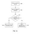
- FIG. 14is a flow chart showing a method of operating a memory system having dual function memory devices.
- the present inventionprovides a dual function memory device architecture compatible with two different modes of operation, such as an asynchronous mode of operation and a synchronous mode of operation.
- Flash memoryis a commonly used type of non-volatile memory in widespread use as mass storage for consumer electronics, such as digital cameras and portable digital music players for example.
- the density of a presently available Flash memory componentconsisting of 2 stacked dies, can be up to 32 Gbits (4 GB), which is suitable for use in popular USB Flash drives, since the size of one Flash component is typically small.
- Flash memory devicesare combined together into a system to effectively increase the available storage capacity. For example, Flash storage densities of 20 GB may be required for such applications.
- FIG. 1Ais a block diagram of a non-volatile memory system 10 integrated with a host system 12 .
- the system 10includes a memory controller 14 in communication with host system 12 , and a plurality of non-volatile memory devices 16 - 1 , 16 - 2 , 16 - 3 and 16 - 4 .
- the non-volatile memory devices 16 - 1 - 16 - 4can be asynchronous flash memory devices.
- the host system 12includes a processing device such as a microcontroller, microprocessor, or a computer system.
- the system 10 of FIG. 1Ais organized to include one channel 18 , with the memory devices 16 - 1 - 16 - 4 being connected in parallel to channel 18 .
- the system 10can have more or fewer than four memory devices connected to it.
- the memory devices 16 - 1 - 16 - 4are asynchronous and connected in parallel with each other.
- Channel 18includes a set of common buses, which include data and control lines that are connected to all of its corresponding memory devices.
- Each memory deviceis enabled or disabled with respective chip select (enable) signals CE1#, CE2#, CE3# and CE4#, provided by memory controller 14 .
- the “#”indicates that the signal is an active low logic level signal.
- one of the chip select signalsis typically selected at one time to enable a corresponding one of the non-volatile memory devices 16 - 1 - 16 - 4 .
- the memory controller 14is responsible for issuing commands and data, via the channel 18 , to a selected memory device in response to the operation of the host system 12 .
- Read data output from the memory devicesis transferred via the channel 18 back to the memory controller 14 and host system 12 .
- the system 10is generally said to include a multi-drop bus, in which the memory devices 16 - 1 - 16 - 4 are connected in parallel with respect to channel 18 .
- FIG. 1Bis a diagram of one of the flash memory devices 16 - 1 - 16 - 4 which can be used in the memory system of FIG. 1A .
- This flash memory deviceincludes several input and output ports, which include for example power supply pins, control pins and data pins.
- the power supply pinsinclude VCC and VSS for supplying power to all the circuits of the flash memory device. Additional power supply pins can be provided for supplying only the input and output buffers, as is well known in the art.
- Table 1 belowprovides a listing of the control and data pins, their corresponding descriptions, definitions, and example logic states. It is noted that that pins are one example physical manifestation of a port, which is used for interconnecting signals or voltages of a packaged device to a board.
- the portscan include other types of connections, such as for example, terminals and contacts for embedded and system-in-package (SIP) systems.
- SIPsystem-in-package
- R/B # Ready/Busythe R/B # is open drain pin and the output signal is used to indicate the operating condition of the device.
- CE # Chip Enablethe device goes into a low-power Standby mode when CE # goes HIGH during the device is in Ready state.
- CLE Command Latch Enablethe CLE input signal is used to control loading of the operation mode command into the internal command register. The command is latched into the command register from the I/O port on the rising edge of the WE # signal while CLE is HIGH.
- ALE Address Latch Enable(ALE): the ALE signal is used to control loading address information into the internal address register. Address information is latched into the address register from the I/O port on the rising edge of the WE # signal while ALE is HIGH.
- WE # Write Enablethe WE # signal is used to control the acquisition of data from the I/O port.
- RE # Read Enablethe RE signal controls serial data output. Data is available after the falling edge of RE #.
- WP # Write Protectthe WP # signal is used to protect the device from accidental programming or erasing. The internal voltage regulator (high voltage generator) is reset when WP # is LOW. This signal is usually used for protecting the data during the power-on/off sequence when input signals are invalid.
- I/O[n] I/O Portpins are used as a port for transferring address, command and input/output data to and from the device. Variable n can be any non-zero integer value.
- chip enable CE#With the exception of the chip enable CE#, all the other pins are coupled to respective global lines that make up channel 18 . Individual chip enable signals are provided to each flash memory device by the memory controller 14 .
- each of the non-volatile memory deviceshas one specific data interface for receiving and providing data.
- thisis a parallel data interface commonly used in asynchronous flash memory devices.
- Standard parallel data interfaces providing multiple bits of data in parallelare known to suffer from well known communication degrading effects such as cross-talk, signal skew and signal attenuation, for example, which degrades signal quality, when operated beyond their rated operating frequency.
- a memory device having a serial data interfacehas been disclosed in commonly owned U.S. Patent Publication No. 20070076479, which receives and provides data serially at a frequency, for example, 200 MHz.
- the memory device described in U.S. Patent Publication No. 20070076479can be used in a system of memory devices that are serially connected to each other, as described in commonly owned U.S. Provisional Patent Application No. 60/902,003 filed Feb. 16, 2007, the content of which is incorporated herein by reference in its entirety.
- FIG. 2Ais a block diagram illustrating the conceptual nature of a serial memory system.
- the serial ring-topology memory system 20includes a memory controller 22 having at least one output port Sout and an input port Sin, and memory devices 24 , 26 , 28 and 30 that are connected in series.
- the memory devicescan be serial interface flash memory devices for example. While not shown in FIG. 2A , each memory device has an Sin input port and an Sout output port. Input and output ports consist of one or more physical pins or connections interfacing the memory device to the system it is a part of.
- the memory devicescan be flash memory devices.
- the memory devicescan be DRAM, SRAM or any other type of memory device provided it has an input/output interface compatible with a specific command structure, for executing commands or for passing commands and data through to the next memory device.
- the current example of FIG. 2Aincludes four memory devices, but alternate configurations can include a single memory device, or any suitable number of memory devices. Accordingly, if memory device 24 is the first device of the system 20 as it is connected to Sout, then memory device 30 is the Nth or last device as it is connected to Sin, where N is an integer number greater than zero. Memory devices 26 to 28 are then intervening serially connected memory devices between the first and last memory devices. In the example of FIG. 2A , the memory devices 26 to 28 are synchronous and connected in series with each other and the memory controller 22 .
- FIG. 2Bis a diagram of the serial interface flash memory device ( 24 to 28 for example) which can be used in the memory system of FIG. 2A .
- This example serial interface flash memory deviceincludes power supply pins, control pins and data pins.
- the power supply pinsinclude VCC and VSS for supplying power to all the circuits of the flash memory device. Additional power supply pins can be provided for supplying only the input and output buffers, as is well known in the art.
- Table 2 belowprovides a listing of the control and data pins, their corresponding descriptions, and example logic states.
- CK/ ClockCK is the system clock input.
- CK and CK#are differential clock inputs. All CK # commands, addresses, input data and output data are referenced to the crossing edges of CK and CK# in both directions.
- CE # Chip EnableWhen CE # is LOW, the device is enabled. Once the device starts a Program or Erase operation, the Chip Enable pin can be de-asserted. In addition, CE# LOW activates and CE# HIGH deactivates the internal clock signals.
- RST # Chip ResetRST# provides a reset for the device. When RST # is HIGH, the device is on the normal operating mode. When RST # is LOW, the device will enter the Reset mode.
- CSI Command Strobe InputWhen CSI is HIGH, command, address and input data through D[n] are latched on the crossing of CK and CK #. When CSI is LOW, the device ignores input signals from D[n].
- CSO Command Strobe OutputEcho signal of CSI.
- DSI Data Strobe InputEnables the Q[n] buffer when HIGH. When DSI is LOW, the Q[n] buffer holds the previous data accessed.
- DSO Data Strobe OutputEcho signal of DSI.
- serially connected memory system of FIG. 2Further details of the serially connected memory system of FIG. 2 are disclosed in commonly owned U.S. patent application Ser. No. 12/032,249 filed on Feb. 15, 2008, which describes a serial memory system in which each memory device receives a parallel clock signal, and a serial memory system in which each memory device receives a source synchronous clock signal.
- the functional pin assignments or definitions of the asynchronous and serial interface flash memory devicesare substantially different from each other, and are accordingly, incompatible with each other. This means that the serial interface flash memory device of FIG. 2B cannot be used in a multi-drop memory system, and correspondingly, the asynchronous flash memory device of FIG. 1B cannot be used in a serial connected ring topology memory system.
- a dual function memory deviceusable in two different operating modes, such as a synchronous mode and an asynchronous mode for example. More specifically, the dual function memory device is compatible with asynchronous and synchronous function or operation.
- the following embodimentsshow an asynchronous flash memory device for parallel connection with a corresponding memory controller, and a synchronous flash memory device for serial connection with a corresponding memory controller.
- the architecture and circuit embodiments to be shown hereinare applicable to other memory devices without limitation to its parallel or serial interconnection to another device.
- An embodiment of the present inventionprovides a dual function memory device architecture compatible with asynchronous operation and synchronous serial operation.
- the dual function memory device architectureincludes one set of ports having two different pinout definitions or functions. Coupled between the ports and core circuits of the memory device are asynchronous and synchronous input and output signal paths or circuits.
- the signal pathsinclude shared or dedicated buffers coupled to the ports, asynchronous and synchronous command decoders, a network of switches, and a mode detector.
- the mode detectordetermines the operating mode of the dual function memory device from a port, and provides the appropriate switch selection signal.
- the network of switchesroutes the input or output signals through the asynchronous or synchronous circuits in response to the switch selection signal.
- the appropriate command decoderinterprets the input signals and provides common control logic with the necessary signals for initiating the corresponding operation.
- FIG. 3is a block diagram of an asynchronous memory device while FIG. 4 is a block diagram of a synchronous serial memory device.
- the asynchronous flash memory device 40 of FIG. 3includes two main circuit blocks.
- the first main circuit blockis the interface and control circuit block consisting of I/O buffers 42 , 44 and 46 , registers 48 , 50 and 52 , and control circuit 54 .
- the output buffer 42drives the R/B# output port
- the control buffers 44include input buffers each connected to a respective input control port
- the data buffers 46include bi-directional buffers for receiving and driving data onto a respective I/O port.
- control buffers 44includes input buffers for the CE#, CLE, ALE, WE#, RE# and WP# input control ports.
- Asynchronous input buffers and output buffer circuitsare well known in the art, and do not need to be described in any further detail.
- a commandis provided via the data I/O ports.
- This commandcan include an operational code (OP code) that corresponds to a specific operation, address information and data, depending on the operation being executed.
- OP codeoperational code
- address and write (program) datacan be more than 8 bits in length, several input iterations or cycles may be required before all the address and write data bits are latched in the proper registers.
- the OP code datais latched in the command register 48 , and address information for read and program operations is latched in address register 50 .
- the OP code datais provided to the control circuit 54 , which includes logic for decoding the OP code, such as a command decoder or interpreter for example.
- the control circuit 54further includes control logic that generates the internal control signals with the required timing for operating both the circuits of the interface and control circuit block, and the circuits of the second main circuit block.
- the second main circuit blockis the core circuitry consisting of a high voltage generator 56 , a row predecoder 58 , a row decoder 60 , a column predecoder 62 , a column decoder 64 , a page buffer 66 , and a memory array 68 .
- the high voltage generator 56can be used for both program and erase operations.
- the following circuit descriptionrelates to a read operation.
- the row predecoder 58receives a row address from address register 50 while the column predecoder 62 receives a column address from address register 50 .
- the predecoded row signalsare used by the row decoder 60 to drive a wordline of memory array 68 for accessing a page of data.
- the data stored in the memory cells connected to the selected wordlineare sensed and stored in the page buffer 66 via bitlines.
- the predecoded column signalsare used by column decoder 64 for selecting a set of 8 bits of data from the page buffer 66 to output to the data buffers 46 . It should be noted that the sequence and timing of asserted control signals originates from the control circuit 54 in response to the received OP code.
- the synchronous serial memory 100 of FIG. 4Aincludes two main circuit blocks.
- the first main circuit blockis the interface and control circuit block consisting of a control interface 102 , a serial interface 104 , an input serial to parallel register block 106 , and an output parallel to serial register block 108 .
- Control interface 102includes input buffer circuits, and generates internal chip select signal chip_sel, internal clock signal sclki, and internal reset signal reset, corresponding to CS#, SCLK and RST# respectively. While signal chip_sel is used primarily by serial interface 104 , reset and sclki are used by many of the circuits throughout memory 100 .
- the second main blockis the core circuitry consisting of memory array 110 , sense amplifier and page buffer circuit 112 , row decoder 114 , column decoder 116 and high voltage generator 118 .
- the circuits of the core circuitrycan be the same as those shown in asynchronous flash memory device 40 of FIG. 3 , which means that they are responsive to the same address, data and control signals received from the interface and control circuit block of synchronous serial memory 100 .
- the main difference between asynchronous flash memory device 40 and synchronous serial memory 100lies in how these control signals are received and provided to the core circuitry. While the interface and control circuit block of asynchronous flash memory device 40 of FIG. 3 is well known, the same named circuit block of synchronous serial memory 100 is quite different.
- Serial interface 104includes input buffers for receiving serial input data D[n], a command strobe input CSI and a data strobe input DSI, and output buffers for providing serial output data Q[n], a command strobe output CSO (echo of CSI) and a data strobe output DSO (echo of DSI). These signals are provided and received at corresponding input/output ports, which as previously discussed can be physical pins, terminals or connectors.
- the input and output buffers of serial interface 104can be implemented with circuits that are well known in the art for buffering input signals and for driving output signals. It is noted however that the input buffers perform a function other than to pass received data to the input serial to parallel register block 106 .
- each input buffer of serial interface 104can pass its received input signal to a corresponding output buffer to provide data flow through functionality.
- the input buffer for CSIpasses the received CSI signal to the output buffer for CSO.
- the input buffer for D[n]passes received data signals to the output buffer for Q[n]
- the input buffer for DSIpasses the received DSI signal to the output buffer for DSO.
- This interfaceallows multiple memory devices having a compatible serial interface to be serially connected to each other, as shown in the memory system of FIG. 2A .
- Serial input D[n]receives this serial data stream, where there can be “n” serial inputs and a corresponding number of “n” serial outputs for realizing higher throughput loading and outputting of data.
- the serial interface 104provides buffered serial input data SER_IN and receives serial output data SER_OUT from output parallel to serial register block 108 .
- the input serial to parallel register block 106receives SER_IN and converts it into a parallel set of signals PAR_IN.
- the input serial to parallel register block 106includes serial to parallel registers for converting the OP code command, data and address bit information into parallel format, and command decoding logic for generating the internal control signals required for controlling the core circuits.
- PAR_INincludes input data DIN, column address C_ADDR, row address R_ADDR, and other control signals (not shown) for activating core circuitry in a particular sequence and/or timing.
- the output parallel-to-serial register block 108receives a parallel set of output data DOUT and converts it into the serial output data SER_OUT, which is subsequently provided as data stream Q[n] through the serial interface 104 . Details of the input serial to parallel register block 106 are shown in FIG. 4B to illustrate how the SER_IN bitstream is converted into parallel address, command and data signals.
- FIG. 4Bis a schematic illustrating an example configuration of the input serial to parallel register block 106 shown in FIG. 4A .
- this circuitreceives the input data stream SER_IN, and converts SER_IN into parallel groups of data.
- SER_INcan be converted to provide a command CMD, a column address C_ADD, a row address R_ADD and input data DATA_IN.
- the input serial-to-parallel register block 106includes a command register 130 , a temporary register 132 , and a serial data register 134 . Since the data structure of the serial input data stream is predetermined, specific numbers of bits of the input data stream are distributed to the aforementioned registers.
- the bits corresponding to a commandcan be stored in the command register 130
- the bits corresponding to row and column addressescan be stored in the temporary register 132
- the bits corresponding to input datacan be stored in the serial data register 134 .
- the distribution of the bits of the serial input data streamcan be controlled by other circuits, in a variety of ways that are not relevant to the embodiments of the present invention.
- the input serial to parallel register block 106includes a command interpreter 136 which receives a command signal in parallel from command register 130 , and generates a decoded command CMD.
- Command interpreter 136is a standard circuit implemented with interconnected logic gates or firmware, for decoding the received commands. While not shown in FIG. 4A or 4 B, decoded command CMD is received by control logic which is responsible for enabling specific circuits of the core circuitry in a particular sequence and/or with a particular timing, depending on the operation being executed.
- a switch controller 138receives one or more signals from CMD to control a simple switch circuit 140 .
- Switch circuit 140receives all the data stored in the temporary register 132 in parallel, and loads one or both of column address register 142 and row/bank register 144 with data in accordance with the decoded command CMD. This decoding is preferably done because the temporary register may not always include both column and row/bank address data. For example, a serial input data stream having a block erase command will only use a row address, in which case only the relevant bits stored in the temporary register 132 are loaded into row/bank register 144 .
- the data register 146receives the converted parallel data directly from serial data register 134 , under the control of the command interpreter 136 . It is noted that all the circuits shown in FIG.
- the column address register 142provides parallel signal C_ADDR
- the row/bank address register 144provides parallel signal R_ADDR
- data register 146provides parallel signal DIN, for programming operations.
- CMD, C_ADDR, R_ADDR and DINform the parallel signal set PAR_IN. Bit widths for each of the parallel signals have not been specified, as the desired width is a design parameter which can be customized, or tailored for a particular design or architecture.
- the interface and control circuit blocks of the asynchronous flash memory 40 and the synchronous serial memory 100are inherently different from each other.
- the differencesare due to the fact that the input control signals received at the pins for the two memory devices are different, each set of signals following a specific signaling protocol in order to properly operate the respective memory device.
- the resulting signals for controlling the core circuitry of each memory deviceare functionally the same since both can use the same core circuitry. Therefore a dual function memory device architecture is formed with this understanding of the input and output signal path differences between the ports and the core circuitry of each memory device.
- FIG. 5is an architectural diagram of a dual function memory device, according to an embodiment of the present invention.
- the dual function memory device 200selectively operates in one of two modes, where each mode responds to a specific set of external signals.
- one modeis an asynchronous mode corresponding to the operation of the asynchronous flash memory device 40
- a second modeis a synchronous serial mode corresponding to the operation of the synchronous serial memory 100 .
- the dual function memory device 200has a plurality of dedicated input, output and bidirectional I/O ports 202 , of which only one is shown to represent the collective set of pins formed in the packaging of the memory device. Specific individual ports 202 are designed to receive two different external signals, meaning for example, a physical package of the dual function memory device 200 includes one set of pins which can be coupled to two different sets of signals originating from a memory controller. Therefore, memory device 200 includes at least all the ports corresponding to the type of memory device having the greater number of ports.
- the dual function memory device 200consists of three main circuit blocks, where the first is the core circuitry 204 , the second is the interface and control circuit block 206 , and the third is the mode detector 208 .
- the core circuitry 204can be the same as the core circuitry shown in FIG. 3 and FIG. 4A , for example.
- the interface and control circuit block 206includes two signal paths between the core circuitry 204 and ports 202 , where only one of the signal paths is active for the selected mode of operation.
- the mode detector 208detects a voltage level of one of the ports 202 , and enables the signal path that corresponds to the set of external signals being applied to the ports 202 .
- the interface and control circuit block 206includes an interface circuit 210 , a selector 212 , and control logic 214 .
- the interface circuit 210includes synchronous circuits 218 and asynchronous circuits 220 selectively coupled to ports 202 , each corresponding to a synchronous signal path and an asynchronous signal path.
- the synchronous serial signal pathincludes synchronous circuits 218 and selector 212 .
- the synchronous circuits 218include input/output buffers, data registers, address registers and any other circuitry that is necessary for conditioning input or output signals provided to and received from core circuitry 204 .
- the synchronous circuits 218can include all the elements of input serial to parallel register block 106 of FIG. 4A , including a synchronous command interpreter.
- the asynchronous signal pathincludes asynchronous circuits 220 and selector 212 .
- the asynchronous circuits 220can include buffers 42 , 44 , 46 , and registers 48 , 50 and 52 shown in FIG. 3 , for conditioning input or output signals provided to and received from core circuitry 204 .
- Each of the synchronous circuits 218 and asynchronous circuits 220provide decoded command signals and core circuit signals, and can receive read data from the memory array.
- Decoded command signals S_DECare provided by the command decoder of synchronous circuits 218
- decoded command signals A_DECare provided by the command decoder of asynchronous circuits 220 .
- Both S_DEC and A_DECare provided to selector 212 that passes only one to the control logic 214 .
- the control logic 214generates the signals necessary for operating the core circuits 204 for all operations, which include read, program and erase operations.
- Core circuit signalsinclude input data, memory address information, or data to be written to the memory array, and other control signals that are used by core circuits 204 . These signals are collectively shown as signal DATA/CTRL in FIG. 5 . These signals are not used by the control logic, and hence are provided directly to core circuits 204 .
- DATA/CTRLfurther includes read data from the memory array provided to the output buffers of either the synchronous circuits 218 or the asynchronous circuits 220 .
- Switch signal MODEis provided by mode detector 208 , which monitors one of the ports 202 .
- Signal MODEis provided to interface circuit 210 for selectively routing external input signals or output signals through either the synchronous circuits 218 or the asynchronous circuits 220 .
- some ports 202 that receive two different external signalsshare the same circuits, and the buffered signal is then routed through the asynchronous or synchronous signal path in response to MODE.
- Other ports 202have different dedicated circuits in order to accommodate the different external signals, hence the port 202 is directly coupled to the selected buffer circuit in response to MODE. Shared buffer circuits thus operate as both synchronous and asynchronous buffer circuits.
- FIG. 5is intended to illustrate the general path of the signals for the synchronous serial signal path and the asynchronous signal path. It should be understood that some signals provided by synchronous circuits 218 and asynchronous circuits 220 are passed directly to selector 212 or directly to core circuitry 204 , such as data and address signals for example, or any other signal that is not required by the corresponding control logic for generating further downstream signals. Correspondingly, read data provided by core circuitry 204 can be passed to circuits 218 and 220 directly or via selector 212 . Both the synchronous serial signal path and the asynchronous signal path can include unidirectional and bidirectional signals. Unidirectional signals include the address signals and control signals provided from ports 202 or control logic 214 , which are used for controlling the core circuits 204 . Bidirectional signals include datalines or databuses that carry read data and program data.
- the mode detector 208provides switch signals MODE, which is used by interface circuit 210 for controlling switching means that route signals through the synchronous circuits 218 or the asynchronous circuits 220 .
- Mode detector 208statically sets MODE to a specific logic level in response to a static voltage level detected on one of ports 202 .
- mode detector 208monitors a voltage level of a specific port 202 during a power up sequence, and determines if this specific port 202 is electrically biased to a specific voltage level, such as a voltage supply level. If the specific port 202 is biased to the specific voltage supply level, then MODE is set to a specific logic level. Otherwise, MODE is set to a different logic level. Accordingly, the voltage level applied to the specific port 202 corresponds to the set of external signals being applied to the other ports 202 .
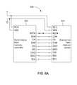
- FIG. 6Ais a schematic showing the interconnection of a flash memory controller with the dual function memory device embodiment of FIG. 5 in an example memory system 300 .
- memory system 300includes a synchronous flash memory controller 302 connected to one dual function memory device 304 , where the dual function memory device 304 can have the architecture shown in FIG. 5 .
- the dual function memory device 304includes the input/output ports previously listed in Table 2.
- the VCC and VSS power suppliesare physically connected to the corresponding VCC and VSS ports of both the synchronous flash memory controller 302 and the dual function memory device 304 .
- the RST# portis monitored by the mode detector 208 of FIG.
- the RST# port of dual function memory device 304can be a bond option that determines the mode of operation of dual function memory device 304 .
- RST#is held at the VSS voltage level during power up to configure dual function memory device 304 to operate in the synchronous serial mode. Therefore the ports will be coupled to the synchronous serial signal path.
- FIG. 6Bis a schematic showing the interconnection of a flash memory controller with the dual function memory device embodiment of FIG. 5 in an example memory system 310 .
- memory system 310includes an asynchronous flash memory controller 312 connected to the same dual function memory device 304 of FIG. 6A .
- the asynchronous flash memory controller 312includes ports for providing and receiving the signals previously listed in Table 1.
- the VCC and VSS power suppliesare physically connected to the corresponding VCC and VSS ports of both the asynchronous flash memory controller 312 and the dual function memory device 304 .
- FIG. 6Billustrates an example assignment of the signals provided by asynchronous flash memory controller 312 to the ports of dual function memory device 304 . As in the example of FIG.
- the RST# portis monitored by the mode detector 208 of FIG. 5 , which is now physically connected to the VCC power supply.
- RST#can be statically held at the VCC level by another circuit, instead of being physically connected to VCC.
- data input port D[n] of dual function memory device 304is not connected to any port of asynchronous flash memory controller 312 , and can be optionally connected to VSS.
- RST#being tied to the VCC power supply during power up signals the dual function memory device 304 to operate in the asynchronous serial mode. Therefore the ports will be coupled to the asynchronous serial signal path.
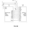
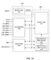
- FIG. 7is a block diagram showing an embodiment of the mode detector 208 and the interface and control circuit block 206 of FIG. 5 .
- the lines interconnecting the circuit blocksmerely illustrates a functional relationship between connected blocks, without detailing the specific signals being used.
- Mode detector 208includes a power supply detector, such as VCC detector 400 , and mode logic 402 .
- VCC detector 400provides a status signal VCC_OK indicating that the power supply VCC has reached the proper level.
- Mode logic 402generates switch signal MODE in response to VCC_OK and buffered reset signal RSTf#.
- buffered reset signal RSTf#is related to external reset signal RST#, and is an active low logic level signal indicated by the “#” symbol appended to the signal name.
- the logic level of MODEwill have one logic level if RST# is held at VCC and another logic level if RST# is held at VSS once VCC_OK is asserted. This means that when VCC_OK is at a logic level indicating that the power supply is at the proper level, the logic state of MODE is sensed and thus determined by the voltage applied to external port RST#. More specific to a specific example, if RST# is tied to VCC, then MODE will be at a logic level corresponding to the asynchronous operating mode. Otherwise, MODE will be at a logic level corresponding to the synchronous serial operating mode. While these two specific operating modes are discussed, those skilled in the art will understand that this technique can be used for determining any two different operating modes.
- the interface and control circuit block 206includes an RST# input buffer 404 , a set of control signal buffers shown as control buffer block 406 , a set of data input and output buffers shown as data buffer block 408 , a global command decoder 410 and control logic 412 .
- the RST# input buffer 404is a dedicated input buffer for external signal RST#, and is considered a part of the synchronous circuits 218 of FIG. 5 because the dual function memory device 200 is responsive to changing logic levels of signal RST# during the synchronous mode of operation.
- the control buffer block 406includes individual input buffers for synchronous serial mode signals CE#, CK, CK#, CSI, DSI and individual output buffers for synchronous serial mode signals CSO and DSO.
- these synchronous serial mode signalsare considered the default signal assignment to the ports coupled to interface and control circuit block 206 .
- specific portshave a secondary signal assigned to them, which appear in brackets.
- the port receiving CK in the synchronous serial mode of operationreceives WE# in the asynchronous mode of operation.
- the assignment of secondary signals to the ports assigned to existing default signalscan be arbitrary. However, in order to minimize additional buffer circuitry in the control buffer block 406 and the data buffer block 408 , the secondary signals are assigned to existing default signals of the same type.
- the portscan be input-type ports or output-type ports. Accordingly, secondary input signals are assigned to default input signal ports and secondary output signals are assigned to default output signal ports. This means that the same input or output buffer circuit is shared for both synchronous serial and asynchronous operating modes. In some circumstances however, buffer circuit sharing of the default signal ports with all secondary signals is not possible when the asynchronous and synchronous serial modes of operation each use a different number of input and output signals.
- an additional input bufferis coupled to the CSO port.
- the port(s) assigned to the default data output signals Q[n]are assigned secondary data input/output signal(s) I/O[n]. Therefore at least an additional input buffer is coupled to each Q[n] port to enable data input functionality in the asynchronous mode of operation.
- control buffer block 406 and data buffer block 408include path switching circuits for routing the buffered signals through either the synchronous serial signal path consisting of the synchronous circuits 218 or the asynchronous signal path consisting of the asynchronous circuits 220 .
- the global command decoder 410is responsible for decoding a command received from the data input ports via the data buffer block 408 , which includes read, program and erase op code commands for example, during both the synchronous serial and asynchronous modes of operation. While both modes of operation may share the same types of commands, there are commands exclusive to each mode. Accordingly global command decoder 410 includes dedicated decoders, one being a synchronous command decoder 414 and the other being an asynchronous command decoder 416 . According to the present embodiments, each of the two command decoders 414 and 416 includes logic and circuits for decoding all the valid commands for the corresponding operating mode.
- the two command decoders 414 and 416can share common logic and circuits for decoding the same bit pattern used in both operating modes that represent the same command.
- the global command decoder 410provides corresponding command signals to the control logic 412 , which then activates the required circuits responsible for executing the command.
- both command decoders 414 and 416receive different signals corresponding to the same operation from the ports, but will provide the same command signals to control logic 412 .
- the command for a program operationis different for the synchronous and the asynchronous modes of operation, but both command decoders 414 and 416 generate identical command signals for enabling control logic 412 to execute the program operation.
- the control logic 412is responsible for providing internal control signals that activate specific circuits of the dual function memory device 200 , in response to the command signals corresponding to the decoded command and to one or more of the external control signals provided by RST# buffer 404 and control buffer block 406 . In the program operation example, the control logic 412 ensures that the wordlines and bitlines are driven with the appropriate voltage levels and in the proper sequence.
- the operating mode of the dual function memory deviceis set by bonding the reset port RST# to a supply voltage, such as VSS or VCC for example, or alternately, RST# can be statically held at either VSS or VCC.
- mode detector 208assesses the voltage level of the RST# port during VCC detection in order to set the operating mode, which can be bonded to a supply voltage or controlled as a reset signal.
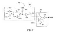
- FIG. 8is an example circuit schematic of the mode detector 208 shown in FIG. 7 .
- FIG. 8shows example circuits for the VCC detector 400 and for the mode detector 402 of the mode detector 208 of FIG. 7 .
- the VCC detector 400is connected to the VCC and VSS power supply, for driving intermediate output signal VCC_OK to the high logic level after VCC has reached a predetermined voltage level.
- the VCC detector 400includes a capacitor 450 connected in series with the drain of a PMOS transistor 452 , the source of which is connected to supply voltage VCC, and the gate of which is connected to ground (VSS).
- a pair of cross-coupled inverters 454 and 456are connected to the shared terminal of capacitor 450 and transistor 452 , and to an input of inverter 458 .
- a capacitor 460is connected between VCC and the input of inverter 458 .
- the output of inverter 458drives output signal VCC_OK.
- the circuit of VCC detector 400can be modified to detect a predetermined voltage other than VCC.
- the circuitcan detect a reference voltage that is below VCC.
- transistor 452In operation, current passes through transistor 452 from VCC when the voltage at node A rises, during power up. Capacitor 460 supplies current from VCC when VCC rises. However, due to the PMOS threshold voltage of transistor 452 , the voltage at node B will be greater than the voltage at node A. The cross-coupled inverters 454 and 456 amplify the difference in voltage between node A and node B, and latch the logic state. At this point, node B is at the high logic level, and VCC_OK is at the low logic level due to the inversion by inverter 458 . As VCC continues to rise, transistor 452 conducts current.
- Transistor 452is typically sized so that when it conducts current, it forces the cross-coupled inverters 454 and 456 to flip logic states. Node A then rises to VCC and node B drops to VSS, and as a result VCC_OK rises to the high logic level.
- the mode detector 402 in the present exampleincludes a pair of cross-coupled NAND logic gates 462 , 464 , and inverter 466 .
- NAND logic gate 462has a first input receiving VCC_OK from VCC detector 402 , and a second input receiving an output of NAND logic gate 464 .
- NAND logic gate 464has a first input receiving an output of NAND logic gate 462 , and a second input receiving buffered reset signal RSTf#.
- Cross-coupled NAND logic gates 462 and 464function as a set-reset latch for latching RSTf# at the low logic level during VCC detection.
- the output of inverter 466is switch signal MODE. MODE can have two different logic levels depending on the logic level of RSTf#.
- MODEsignals to the internal circuits that the dual function memory device is operating in the asynchronous mode. In another and opposite logic level, MODE signals to the internal circuits that the dual function memory device is operating in the synchronous serial mode.
- These internal circuitsinclude the interface and control circuit block 206 of FIG. 7 for example.
- the operation of mode detector 402is illustrated with reference to the timing diagrams of FIGS. 9A and 9B .
- FIG. 9Ais the timing diagram showing how the synchronous serial mode of operation is detected.
- the output signal VCC_OKis driven to the high logic level by VCC detector 400 after VCC reaches the predetermined target level.
- the mode logic 402then compares VCC_OK with the output signal RSTf#, where the level of RSTf# follows that of RST#.
- FIG. 9Bis the timing diagram showing how the asynchronous mode of operation is detected.
- RST#is maintained at the VCC power supply level. This can be done by physically bonding RST# to VCC, or by statically holding RST# at the high logic level corresponding to VCC. In either case, RST# and RSTf# will follow VCC since it is presumed that the circuit maintaining RST# at VCC receives the same global supply voltages.
- the voltage applied to the VCC portrises from ground towards VCC, and the output signal VCC_OK is eventually driven to the high logic level by VCC detector 400 after VCC reaches the predetermined target level.
- the mode logic 402then compares VCC_OK with the output signal RSTf#.
- RSTf#is at the high logic level when VCC_OK reaches the high logic level
- MODEremains at the low logic level to set the interface and control circuit block 206 of FIG. 7 to operate in the asynchronous mode.
- the chip enable portcan be statically held at VCC during power up, in which case it has a signal trace that follows the dashed line that tracks with VCC. Otherwise, CE# can be driven to the high logic level after VCC_OK rises to the high logic level.
- an existing portsuch as the reset port RST# is used for setting the operating mode of the dual function memory device.
- RST#is a signal used in only one of the two operating modes.
- the previously described embodimentsare not limited to using a RST# port, but any port that is only used in one of the two operating modes.
- a dedicated port for selecting the operating modecan be added to the dual function memory device for setting the operating mode.
- FIG. 10is a block diagram showing an alternate embodiment of the mode detector 208 and the interface and control circuit block 206 of FIG. 7 , in which a dedicated port MODE is used for selecting between the synchronous serial and asynchronous modes of operation.
- mode detector 208includes a MODE input buffer 480 coupled to the MODE port for providing internal mode signal MODE
- the interface and control circuit block 206is substantially the same as the same numbered interface and control circuit block of FIG. 7 .
- control buffer block 482 of FIG. 10includes the input buffer circuits for the reset port RST#.
- each portcan have shared buffers or dedicated buffers.
- FIG. 10each port can have shared buffers or dedicated buffers.
- the RST# portis used as it would normally be used in the synchronous serial mode of operation, but is not used in the asynchronous mode of operation.
- the MODE buffer 480includes standard input signal conditioning circuits, which can be similar or identical to those used in control buffer block 482 for other input signals.
- the function of MODE in the FIG. 10is the same as that in FIG. 7 , where the logic level of MODE sets the circuits of the interface and control circuit block 206 to operate in either the asynchronous mode or the synchronous serial mode.
- the MODE portcan either be physically bonded to either VDD or VSS, or statically held at either VDD or VSS in order to set the operating mode of the dual function memory device. With either technique, MODE is set to VDD or VSS.
- global command decoder 410includes two different control signal paths.
- synchronous command decoder 414is included within synchronous circuits 218 .
- asynchronous command decoder 416is included within asynchronous circuits 220 .
- the global command decoder 410can include the selector 212 of FIG. 5 integrated within it, so that the appropriate set of command signals are coupled to control logic 412 .
- FIG. 11is a block diagram illustrating the circuit blocks in the aforementioned synchronous signal path and asynchronous signal path.
- the synchronous control signal pathincludes the synchronous command decoder 414 and selector 216
- the asynchronous control signal pathincludes the asynchronous command decoder 416 and selector 216 .
- the synchronous command decoder 414receives a set of signals S_CMD corresponding to a synchronous mode command, also referred to as an op code, from the data buffer block 408 .
- the decoded command signal S_DECis provided to one input of selector 212 .
- the asynchronous command decoder 416receives a set of signals A_CMD corresponding to an asynchronous mode command, also referred to as an op code, from the data buffer block 408 .
- the decoded command signal A_DECis provided to a second input of selector 212 .
- Selector 212couples either A_DEC or S_DEC to control logic 412 in response to switch signal MODE.
- the control logic 412generates the necessary internal control signals, collectively indicated as CORE_CTRL in FIG. 11 , which are used by specific circuits in the core circuitry 204 .
- the set of signals CORE_CTRLcan be a set of any activated signals required for executing a particular operation. Those skilled in the art should understand that a programming operation requires different internal control signals than that of a read operation, for example.
- control buffer block 406 / 482 and data buffer block 408 of FIGS. 7 and 10have ports with either shared buffer circuits or dedicated buffer circuits.
- An input or output buffer circuit for a default signalcan be shared if the secondary signal assigned to the port is of the same type.
- both the default and secondary signalscan be of the input type or of the output type, for example.
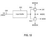
- FIG. 12is a circuit schematic example of a buffer circuit for clock port CK used by the dual function memory device in the synchronous serial mode of operation.
- secondary signal WE# for the asynchronous mode of operationis assigned to the CK port.
- the buffer for CKincludes a well known input buffer 500 and a signal path switch consisting of pass gates 502 and 504 .
- Input buffer 500receives a signal received at port 506 , and provides a corresponding buffered signal at its output.
- the inputs of pass gates 502 and 504receive the buffered signal in parallel, and selectively passes it as an internal clock signal CKf or as an internal WEf# signal in response to the logic level of MODE and its complement, MODE#.
- MODEis at the high logic level to set the dual function memory device to operate in the synchronous serial mode. Therefore, signal CK is connected to port 506 and pass gate 502 is turned on while pass gate 504 is turned off. Internal signal CKf is then passed to other circuits, such as the synchronous control logic 418 of FIGS. 7 and 10 for example.
- MODEis at the low logic level, the dual function memory device is set to operate in the asynchronous mode. Therefore, signal WE# is connected to CK port 506 and pass gate 502 is turned off while pass gate 504 is turned on. Internal signal WEf# is then passed to other circuits, such as the asynchronous control logic 420 of FIGS. 7 and 10 for example. As can be seen in FIG. 12 , input buffer 500 is shared by both signals CK and WE#.
- FIG. 13is a circuit schematic example of the buffers for the input data port Dn and the output data port Qn.
- the Dn bufferincludes a serial input block 510 and optional power savings means, including power switch 512 .
- the serial input block 510includes other circuits, such as an input buffer from serial interface 105 of FIG.
- PAR_INincludes the command information CMD, which is provided to the synchronous command decoder 414 of FIGS. 7 and 10 .
- the dual function memory devicepasses the data received at its Dn input port to a subsequent device through its Qn output port. Therefore the serial input block 510 provides flow through data F_DATA that is received by the buffer for the Qn port.
- the Qn bufferincludes a unidirectional data output path and a bi-directional data path.
- the unidirectional data output pathis enabled during the synchronous serial mode of operation, and the bi-directional data path is enabled during the asynchronous mode of operation.
- the unidirectional data output pathincludes serial output block 516 , pass gate 518 , pass gate 520 and power switch 522 .
- Pass gate 518 , serial output block 516 and pass gate 520are connected in series for coupling read data DOUT provided by the core circuits of the dual function memory device, to Qn port 524 during the synchronous serial mode of operation.
- DOUTis provided as a parallel set of signals
- the serial output block 516can include the output parallel-to-serial register block 108 of FIG.
- the output parallel-to-serial register block 108converts DOUT and converts into a serial output data SER_OUT.
- Qncorresponds to either F_DATA provided from the serial input block 510 or to read data DOUT provided from the core circuitry. The selection of which source of data to output is controlled by the synchronous control logic 418 of FIGS. 7 and 10 based on the operation being executed.
- the bi-directional data pathis provided to accommodate the secondary assignment of the input/output data signal I/On.
- the bidirectional data pathincludes a pass gate 526 , I/O buffer 528 , pass gate 530 and power switch 532 .
- Pass gate 526 , I/O buffer 528 and pass gate 530are connected in series for bi-directionally coupling input/output data DI/O to the Qn port 524 .
- I/O buffer 528includes an output buffer for driving read data onto the Qn port 524 , and an input buffer for receiving data applied to the Qn port 524 .
- I/O buffer 528can include the same circuits as data buffers 46 of FIG. 3 .
- DI/Ocan be either read data from the core circuitry or command information that includes an op code, a read address, a write address, and optional write data.
- the op code portion of DI/Ois provided to asynchronous command decoder 416 .
- the power switches 512 , 522 and 532couple VCC power to all the circuits within serial input block 510 , serial output block 516 and I/O buffer 528 .
- MODEis at the high logic level to turn of power switch 532 and pass gates 526 and 530 .
- the I/O buffer 528is isolated from DI/O and Qn port 524 , and disabled as its circuits no longer receive VCC.
- the bi-directional data pathis disabled during the synchronous serial mode of operation, and power savings is realized since there is no further power consumption due to logic gate switching.
- MODEis at the low logic level. Therefore power switches 512 and 522 , and pass gates 518 and 520 are turned off for disabling serial input block 510 and the unidirectional data output path. Accordingly, serial output block 516 is isolated from DOUT and Qn port 524 .
- asynchronous command decoder 416 and asynchronous control logic 420can be powered by VCC through at least one power switch similar to the power switches shown in FIGS. 12 and 13 , such that they receive VCC power only when the dual function memory device is set to operate in the asynchronous mode.
- synchronous command decoder 414 and synchronous control logic 418can be powered by VCC through at least one power switch. Hence, the circuits that are not used in one operating mode can be turned off to reduce power consumption.
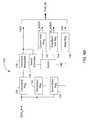
- FIG. 14is a flow chart summarizing the procedure for setting the operating mode of the dual function memory device, according to an embodiment of the present invention. It is assumed that the memory system includes a memory controller connected in a series ring topology with at least one dual function memory device incorporating the previously described embodiments. By example, the memory system can be configured as shown in either FIG. 6A or 6 B.
- the memory systemis powered up, meaning that VCC power is applied to the VCC terminal feeding all the dual function memory devices and the memory controller.
- a designated mode porteither being an existing port such as RST# or a dedicated port such as MODE for example, of each dual function memory device is monitored by its respective mode detector.
- the mode detectorcan be mode detector 208 of FIGS. 7 and 10 for example.
- the mode detector of each dual function memory devicedetermines if its mode port is biased to a supply voltage or not.
- the mode portcan be biased to VCC for setting the asynchronous mode of operation. If its mode port is biased to VCC then its internal switch signal MODE is set to VSS, indicating that the dual function memory device is to operate in the asynchronous mode of operation. Accordingly, the method proceeds to step 606 and the interface and control circuit block 206 of each dual function memory device is dynamically configured to receive asynchronous signals on its ports and to operate the internal circuits with internal control signals generated from the received asynchronous signals.
- step 604if the mode port is held at VSS by the memory controller during power up, then MODE is set to VCC. Accordingly, the method proceeds to step 608 and the interface and control circuit block 206 of each dual function memory device is dynamically configured to receive synchronous signals on its ports and to operate the internal circuits with internal control signals generated from the received synchronous signals.
- the previously described embodimentsenable a memory device, such as a flash memory device, to operate in a synchronous serial mode and the more commonly known asynchronous mode by biasing a port of the memory device package to a specific voltage level during power up.
- the specific voltage levelcan be a supply voltage, or any predetermined voltage level that is detectable by the memory device, and when detected, an internal switch signal having a corresponding logic level is provided. Since different signals are assigned to the ports of the memory device depending on the set operating mode, path switch circuits ensure that the signals corresponding to each operating mode are provided to the corresponding controller circuits in response to the internal switch signal.
- the controller circuitsprovides a set of control signals having the appropriate timing parameters for properly controlling the core circuitry of the memory device in accordance with the set mode of operation.
- the device elementsare connected to each other as shown in the figures, for the sake of simplicity.
- devices, elements, circuits, etc.may be connected directly to each other.
- devices, elements, circuits etc.may be connected indirectly to each other through other devices, elements, circuits, etc., necessary for operation of the apparatus.
- the circuit elements and devicesare directly or indirectly coupled with, or connected to, each other.
Landscapes
- Engineering & Computer Science (AREA)
- Power Engineering (AREA)
- Read Only Memory (AREA)
- Static Random-Access Memory (AREA)
Abstract
Description
| TABLE 1 | |
| Pin | Description |
| R/B # | Ready/Busy: the R/B # is open drain pin and the output signal is used to indicate |
| the operating condition of the device. The R/B # signal is in Busy state (R/B # = | |
| LOW) during the Program, Erase and Read operations and will return to Ready | |
| state (R/B # = HIGH) after completion of the operation. | |
| CE # | Chip Enable: the device goes into a low-power Standby mode when CE # goes |
| HIGH during the device is in Ready state. The CE # signal is ignored when device | |
| is in Busy state (R/B # = LOW), such as during a Program or Erase or Read | |
| operation, and will not enter Standby mode even if the CE # input goes HIGH | |
| CLE | Command Latch Enable: the CLE input signal is used to control loading of the |
| operation mode command into the internal command register. The command is | |
| latched into the command register from the I/O port on the rising edge of the WE # | |
| signal while CLE is HIGH. | |
| ALE | Address Latch Enable (ALE): the ALE signal is used to control loading address |
| information into the internal address register. Address information is latched into | |
| the address register from the I/O port on the rising edge of the WE # signal while | |
| ALE is HIGH. | |
| WE # | Write Enable: the WE # signal is used to control the acquisition of data from the I/O |
| port. | |
| RE # | Read Enable: the RE signal controls serial data output. Data is available after the |
| falling edge of RE #. | |
| WP # | Write Protect: the WP # signal is used to protect the device from accidental |
| programming or erasing. The internal voltage regulator (high voltage generator) is | |
| reset when WP # is LOW. This signal is usually used for protecting the data during | |
| the power-on/off sequence when input signals are invalid. | |
| I/O[n] | I/O Port: pins are used as a port for transferring address, command and |
| input/output data to and from the device. Variable n can be any non-zero integer | |
| value. | |
| TABLE 2 | |
| Pin | Description |
| CK/ | Clock: CK is the system clock input. CK and CK# are differential clock inputs. All |
| CK # | commands, addresses, input data and output data are referenced to the crossing |
| edges of CK and CK# in both directions. | |
| CE # | Chip Enable: When CE # is LOW, the device is enabled. Once the device starts a |
| Program or Erase operation, the Chip Enable pin can be de-asserted. In addition, | |
| CE# LOW activates and CE# HIGH deactivates the internal clock signals. | |
| RST # | Chip Reset: RST# provides a reset for the device. When RST # is HIGH, the device |
| is on the normal operating mode. When RST # is LOW, the device will enter the | |
| Reset mode. | |
| D[n] | Data Input: (n = 1,2,3,4,5,6,7 or 8) receives command, address and input data. If |
| the device is configured in ‘1-bit Link mode (=default)’, D1 is the only valid signal | |
| and receives one byte of packet in 8 crossings of CK/CK #. If the device is | |
| configured in ‘2-bit Link mode’, D1 & D2 are only valid signals and receive one | |
| byte of packet in 4 crossings of CK/CK#. Unused input pins are grounded. | |
| Q[n] | Data Output: (n = 1,2,3,4,5,6,7 or 8) transmits output data during read operation. If |
| device is configured in ‘1-bit Link mode (=default)’, Q1 is the only valid signal and | |
| transmits one byte of packet in 8 crossings of CK/CK#. If the device is configured | |
| in ‘2-bit Link mode’, Q1 & Q2 are the only valid signals and transmit one byte of | |
| packet in 4 crossings of CK/CK #. Unused output pins are DNC (=Do Not | |
| Connect). | |
| CSI | Command Strobe Input: When CSI is HIGH, command, address and input data |
| through D[n] are latched on the crossing of CK and CK #. When CSI is LOW, the | |
| device ignores input signals from D[n]. | |
| CSO | Command Strobe Output: Echo signal of CSI. |
| DSI | Data Strobe Input: Enables the Q[n] buffer when HIGH. When DSI is LOW, the |
| Q[n] buffer holds the previous data accessed. | |
| DSO | Data Strobe Output: Echo signal of DSI. |
Claims (10)
Priority Applications (11)
| Application Number | Priority Date | Filing Date | Title |
|---|---|---|---|
| US12/258,056US7983099B2 (en) | 2007-12-20 | 2008-10-24 | Dual function compatible non-volatile memory device |
| JP2010538289AJP2011507141A (en) | 2007-12-20 | 2008-12-11 | Dual function non-volatile memory device |
| CN201310057323.XACN103151074A (en) | 2007-12-20 | 2008-12-11 | Dual function compatible non-volatile memory device |
| EP08864264AEP2223302A4 (en) | 2007-12-20 | 2008-12-11 | Dual function compatible non-volatile memory device |
| PCT/CA2008/002180WO2009079752A1 (en) | 2007-12-20 | 2008-12-11 | Dual function compatible non-volatile memory device |
| CN200880114400.8ACN101842846B (en) | 2007-12-20 | 2008-12-11 | Dual function compatible non-volatile memory device |
| KR1020107009087AKR20100105537A (en) | 2007-12-20 | 2008-12-11 | Dual function compatible non-volatile memory device |
| TW097148982ATW200943299A (en) | 2007-12-20 | 2008-12-16 | Dual function compatible non-volatile memory device |
| US13/159,060US8270244B2 (en) | 2007-12-20 | 2011-06-13 | Dual function compatible non-volatile memory device |
| US13/592,953US8559261B2 (en) | 2007-12-20 | 2012-08-23 | Dual function compatible non-volatile memory device |
| US14/026,359US8837237B2 (en) | 2007-12-20 | 2013-09-13 | Dual function compatible non-volatile memory device |
Applications Claiming Priority (2)
| Application Number | Priority Date | Filing Date | Title |
|---|---|---|---|
| US1536607P | 2007-12-20 | 2007-12-20 | |
| US12/258,056US7983099B2 (en) | 2007-12-20 | 2008-10-24 | Dual function compatible non-volatile memory device |
Related Child Applications (1)
| Application Number | Title | Priority Date | Filing Date |
|---|---|---|---|
| US13/159,060DivisionUS8270244B2 (en) | 2007-12-20 | 2011-06-13 | Dual function compatible non-volatile memory device |
Publications (2)
| Publication Number | Publication Date |
|---|---|
| US20090161451A1 US20090161451A1 (en) | 2009-06-25 |
| US7983099B2true US7983099B2 (en) | 2011-07-19 |
Family
ID=40788433
Family Applications (4)
| Application Number | Title | Priority Date | Filing Date |
|---|---|---|---|
| US12/258,056Active2029-11-19US7983099B2 (en) | 2007-12-20 | 2008-10-24 | Dual function compatible non-volatile memory device |
| US13/159,060ActiveUS8270244B2 (en) | 2007-12-20 | 2011-06-13 | Dual function compatible non-volatile memory device |
| US13/592,953ActiveUS8559261B2 (en) | 2007-12-20 | 2012-08-23 | Dual function compatible non-volatile memory device |
| US14/026,359ActiveUS8837237B2 (en) | 2007-12-20 | 2013-09-13 | Dual function compatible non-volatile memory device |
Family Applications After (3)
| Application Number | Title | Priority Date | Filing Date |
|---|---|---|---|
| US13/159,060ActiveUS8270244B2 (en) | 2007-12-20 | 2011-06-13 | Dual function compatible non-volatile memory device |
| US13/592,953ActiveUS8559261B2 (en) | 2007-12-20 | 2012-08-23 | Dual function compatible non-volatile memory device |
| US14/026,359ActiveUS8837237B2 (en) | 2007-12-20 | 2013-09-13 | Dual function compatible non-volatile memory device |
Country Status (7)
| Country | Link |
|---|---|
| US (4) | US7983099B2 (en) |
| EP (1) | EP2223302A4 (en) |
| JP (1) | JP2011507141A (en) |
| KR (1) | KR20100105537A (en) |
| CN (2) | CN103151074A (en) |
| TW (1) | TW200943299A (en) |
| WO (1) | WO2009079752A1 (en) |
Cited By (3)
| Publication number | Priority date | Publication date | Assignee | Title |
|---|---|---|---|---|
| US9471484B2 (en) | 2012-09-19 | 2016-10-18 | Novachips Canada Inc. | Flash memory controller having dual mode pin-out |
| US9793894B1 (en)* | 2016-11-18 | 2017-10-17 | Via Alliance Semiconductor Co., Ltd. | Data synchronizer for registering a data signal into a clock domain |
| US10401427B2 (en) | 2016-11-18 | 2019-09-03 | Via Alliance Semiconductor Co., Ltd. | Scannable data synchronizer |
Families Citing this family (35)
| Publication number | Priority date | Publication date | Assignee | Title |
|---|---|---|---|---|
| US7613049B2 (en)* | 2007-01-08 | 2009-11-03 | Macronix International Co., Ltd | Method and system for a serial peripheral interface |
| KR100873617B1 (en)* | 2007-04-12 | 2008-12-12 | 주식회사 하이닉스반도체 | Active Driver Control Circuit of Semiconductor Memory Device |
| US7983099B2 (en) | 2007-12-20 | 2011-07-19 | Mosaid Technologies Incorporated | Dual function compatible non-volatile memory device |
| US7920431B2 (en)* | 2008-06-02 | 2011-04-05 | Micron Technology, Inc. | Asynchronous/synchronous interface |
| KR101165966B1 (en)* | 2010-04-27 | 2012-07-18 | 삼성전자주식회사 | Memory system being accessed as a synchronous mode or an asynchronous mode by command |
| US9063849B2 (en) | 2010-09-17 | 2015-06-23 | Aplus Flash Technology, Inc. | Different types of memory integrated in one chip by using a novel protocol |
| US9703706B2 (en)* | 2011-02-28 | 2017-07-11 | Oracle International Corporation | Universal cache management system |
| US8856482B2 (en) | 2011-03-11 | 2014-10-07 | Micron Technology, Inc. | Systems, devices, memory controllers, and methods for memory initialization |
| US9647668B2 (en)* | 2012-01-13 | 2017-05-09 | Altera Corporation | Apparatus for flexible electronic interfaces and associated methods |
| CN102543189A (en)* | 2012-02-28 | 2012-07-04 | 北京忆恒创源科技有限公司 | Semiconductor memory, interface circuit and access method thereof |
| US9177616B2 (en)* | 2012-10-04 | 2015-11-03 | Cypress Semiconductor Corporation | Supply power dependent controllable write throughput for memory applications |
| CN103794190B (en)* | 2012-10-26 | 2016-08-10 | 纬创资通股份有限公司 | Connection device with electrostatic discharge protection |
| US10289186B1 (en)* | 2013-10-31 | 2019-05-14 | Maxim Integrated Products, Inc. | Systems and methods to improve energy efficiency using adaptive mode switching |
| CN103632717A (en)* | 2013-11-28 | 2014-03-12 | 苏州贝克微电子有限公司 | Digital static CMOS (Complementary Metal-Oxide-Semiconductor Transistor) element |
| TWI553641B (en)* | 2013-12-09 | 2016-10-11 | 慧榮科技股份有限公司 | Data storage device and mode detection method thereof |
| US9362293B2 (en) | 2013-12-20 | 2016-06-07 | Cypress Semiconductor Corporation | CT-NOR differential bitline sensing architecture |
| KR20150116174A (en)* | 2014-04-07 | 2015-10-15 | 에스케이하이닉스 주식회사 | Non-volatile memory device and method of operating the same |
| US9455027B1 (en)* | 2014-08-08 | 2016-09-27 | Cypress Semiconductor Corporation | Power management system for high traffic integrated circuit |
| US10505704B1 (en)* | 2015-08-02 | 2019-12-10 | Wave Computing, Inc. | Data uploading to asynchronous circuitry using circular buffer control |
| KR102316279B1 (en)* | 2015-10-19 | 2021-10-22 | 삼성전자주식회사 | Non-volatile memory device and solid state drive including the same |
| CN105355229A (en)* | 2015-10-29 | 2016-02-24 | 同济大学 | Write circuit and read circuit of asynchronous circuit system for synchronous random-access memory |
| JP2018022383A (en)* | 2016-08-04 | 2018-02-08 | 東芝メモリ株式会社 | Memory system |
| CN109478162B (en)* | 2016-09-26 | 2023-01-03 | 株式会社日立制作所 | Semiconductor memory device with a plurality of memory cells |
| KR102669909B1 (en)* | 2016-12-20 | 2024-05-29 | 에스케이하이닉스 주식회사 | Memory system and operating method thereof |
| US10466766B2 (en)* | 2017-11-09 | 2019-11-05 | Qualcomm Incorporated | Grouping central processing unit memories based on dynamic clock and voltage scaling timing to improve dynamic/leakage power using array power multiplexers |
| JP7223503B2 (en)* | 2018-02-28 | 2023-02-16 | ラピスセミコンダクタ株式会社 | SERIAL INTERFACE CIRCUIT, SEMICONDUCTOR DEVICE, AND SERIAL-PARALLEL CONVERSION METHOD |
| US11606721B2 (en)* | 2019-02-28 | 2023-03-14 | Qualcomm Incorporated | Timing configuration of a layer-1 millimeter wave repeater |
| DE102019002624A1 (en)* | 2019-04-10 | 2020-10-15 | Infineon Technologies Ag | Electronic circuit and method for initializing an electronic circuit |
| JP7589087B2 (en)* | 2021-03-30 | 2024-11-25 | キオクシア株式会社 | Semiconductor memory device |
| KR20220147819A (en)* | 2021-04-28 | 2022-11-04 | 삼성전자주식회사 | Serializer and memory device including the same |
| CN113656342B (en)* | 2021-08-24 | 2022-05-03 | 深圳市康冠商用科技有限公司 | USB interface switching control method and device, all-in-one machine equipment and storage medium |
| KR102586223B1 (en)* | 2022-02-17 | 2023-10-06 | 주식회사 키파운드리 | eFuse OTP memory comprising seral interface logic and operating method thereof |
| JP2023127385A (en)* | 2022-03-01 | 2023-09-13 | キオクシア株式会社 | memory system |
| US20240356544A1 (en)* | 2023-04-21 | 2024-10-24 | Xilinx, Inc. | DFxNoC - A MULTI-PROTOCOL, MULTI-CAST, AND MULTI-ROOT NETWORK-ON-CHIP WITH DYNAMIC RESOURCE ALLOCATION |
| CN116527034A (en)* | 2023-06-26 | 2023-08-01 | 青岛本原微电子有限公司 | Filtering sampling circuit for IO input of chip |
Citations (88)
| Publication number | Priority date | Publication date | Assignee | Title |
|---|---|---|---|---|
| US4174536A (en) | 1977-01-21 | 1979-11-13 | Massachusetts Institute Of Technology | Digital communications controller with firmware control |
| US4733376A (en) | 1984-10-17 | 1988-03-22 | Fujitsu Limited | Semiconductor memory device having serial data input circuit and serial data output circuit |
| US4796231A (en) | 1985-01-22 | 1989-01-03 | Texas Instruments Incorporated | Serial accessed semiconductor memory with reconfigurable shift registers |
| US5126808A (en) | 1989-10-23 | 1992-06-30 | Advanced Micro Devices, Inc. | Flash EEPROM array with paged erase architecture |
| US5136292A (en) | 1989-03-15 | 1992-08-04 | Oki Electric Industry Co., Ltd. | Serial data receiving circuit for serial to parallel conversion |
| US5175819A (en) | 1990-03-28 | 1992-12-29 | Integrated Device Technology, Inc. | Cascadable parallel to serial converter using tap shift registers and data shift registers while receiving input data from FIFO buffer |
| US5243703A (en) | 1990-04-18 | 1993-09-07 | Rambus, Inc. | Apparatus for synchronously generating clock signals in a data processing system |
| US5280539A (en) | 1992-01-15 | 1994-01-18 | Samsung Electronics Co., Ltd. | Synchronous circuit for serial input signal |
| US5319598A (en) | 1990-12-10 | 1994-06-07 | Hughes Aircraft Company | Nonvolatile serially programmable devices |
| US5365484A (en) | 1993-08-23 | 1994-11-15 | Advanced Micro Devices, Inc. | Independent array grounds for flash EEPROM array with paged erase architechture |
| US5404460A (en) | 1994-01-28 | 1995-04-04 | Vlsi Technology, Inc. | Method for configuring multiple identical serial I/O devices to unique addresses through a serial bus |
| US5430859A (en) | 1991-07-26 | 1995-07-04 | Sundisk Corporation | Solid state memory system including plural memory chips and a serialized bus |
| US5440694A (en) | 1992-03-26 | 1995-08-08 | Nec Corporation | Interface circuit for allowing receiving serial data input after receiving serial input suspension signal |
| US5452259A (en) | 1993-11-15 | 1995-09-19 | Micron Technology Inc. | Multiport memory with pipelined serial input |
| US5473563A (en) | 1993-01-13 | 1995-12-05 | Samsung Electronics Co., Ltd. | Nonvolatile semiconductor memory |
| US5473566A (en) | 1994-09-12 | 1995-12-05 | Cirrus Logic, Inc. | Memory architecture and devices, systems and methods utilizing the same |
| US5473577A (en) | 1993-03-20 | 1995-12-05 | Hitachi, Ltd. | Serial memory |
| US5596724A (en) | 1994-02-04 | 1997-01-21 | Advanced Micro Devices | Input/output data port with a parallel and serial interface |
| US5602780A (en) | 1993-10-20 | 1997-02-11 | Texas Instruments Incorporated | Serial to parallel and parallel to serial architecture for a RAM based FIFO memory |
| US5636342A (en) | 1995-02-17 | 1997-06-03 | Dell Usa, L.P. | Systems and method for assigning unique addresses to agents on a system management bus |
| US5671178A (en) | 1995-02-04 | 1997-09-23 | Samsung Electronics Co., Ltd. | Erase verifying circuit for a nonvolatile semiconductor memory with column redundancy |
| US5721840A (en) | 1993-09-20 | 1998-02-24 | Olympus Optical Co., Ltd. | Information processing apparatus incorporating automatic SCSI ID generation |
| US5729683A (en) | 1995-05-18 | 1998-03-17 | Compaq Computer Corporation | Programming memory devices through the parallel port of a computer system |
| US5740379A (en) | 1994-08-19 | 1998-04-14 | Siemens Aktiengesellschaft | Method for generating unique addresses for electrical devices from input bit patterns being verifiable for admissibility |
| US5761146A (en) | 1995-12-28 | 1998-06-02 | Samsung Electronics Co., Ltd. | Data in/out channel control circuit of semiconductor memory device having multi-bank structure |
| US5771199A (en) | 1995-12-29 | 1998-06-23 | Samsung Electronics Co., Ltd. | Integrated circuit memory devices having improved dual memory bank control capability and methods of operating same |
| US5802006A (en) | 1996-02-21 | 1998-09-01 | Nec Corporation | Semiconductor memory of multiple-bank structure having block write function |
| US5818785A (en) | 1995-12-20 | 1998-10-06 | Kabushiki Kaisha Toshiba | Semiconductor memory device having a plurality of banks |
| US5828899A (en) | 1996-01-04 | 1998-10-27 | Compaq Computer Corporation | System for peripheral devices recursively generating unique addresses based on the number of devices connected dependent upon the relative position to the port |
| US5835935A (en) | 1995-09-13 | 1998-11-10 | Lexar Media, Inc. | Method of and architecture for controlling system data with automatic wear leveling in a semiconductor non-volatile mass storage memory |
| US5859809A (en) | 1996-12-31 | 1999-01-12 | Hyundai Electronics Industries Co., Ltd. | Semiconductor device of daisy chain structure having independent refresh apparatus |
| US5872994A (en) | 1995-11-10 | 1999-02-16 | Nec Corporation | Flash memory incorporating microcomputer having on-board writing function |
| US5937425A (en) | 1997-10-16 | 1999-08-10 | M-Systems Flash Disk Pioneers Ltd. | Flash file system optimized for page-mode flash technologies |
| US5941974A (en) | 1996-11-29 | 1999-08-24 | Motorola, Inc. | Serial interface with register selection which uses clock counting, chip select pulsing, and no address bits |
| US5959930A (en) | 1997-08-22 | 1999-09-28 | Mitsubishi Denki Kabushiki Kaisha | Multi-bank synchronous semiconductor memory device |
| US5995417A (en) | 1998-10-20 | 1999-11-30 | Advanced Micro Devices, Inc. | Scheme for page erase and erase verify in a non-volatile memory array |
| US5995405A (en) | 1998-10-27 | 1999-11-30 | Micron Technology, Inc. | Memory module with flexible serial presence detect configuration |
| US6002638A (en) | 1998-01-20 | 1999-12-14 | Microchip Technology Incorporated | Memory device having a switchable clock output and method therefor |
| US6085290A (en) | 1998-03-10 | 2000-07-04 | Nexabit Networks, Llc | Method of and apparatus for validating data read out of a multi port internally cached dynamic random access memory (AMPIC DRAM) |
| US6091660A (en) | 1997-10-02 | 2000-07-18 | Hitachi, Ltd. | Semiconductor integrated circuit device |
| US6107658A (en) | 1997-02-27 | 2000-08-22 | Kabushiki Kaisha Toshiba | Non-volatile semiconductor memory device |
| US6144576A (en) | 1998-08-19 | 2000-11-07 | Intel Corporation | Method and apparatus for implementing a serial memory architecture |
| US6148364A (en) | 1997-12-30 | 2000-11-14 | Netlogic Microsystems, Inc. | Method and apparatus for cascading content addressable memory devices |
| US6178135B1 (en) | 1998-12-28 | 2001-01-23 | Samsung Electronics Co., Ltd. | Multi-bank memory devices having bank selection switches therein that enable efficient sense amplifier utilization |
| US6230233B1 (en) | 1991-09-13 | 2001-05-08 | Sandisk Corporation | Wear leveling techniques for flash EEPROM systems |
| WO2001069411A2 (en) | 2000-03-10 | 2001-09-20 | Arc International Plc | Memory interface and method of interfacing between functional entities |
| US6304921B1 (en) | 1998-12-07 | 2001-10-16 | Motorola Inc. | System for serial peripheral interface with embedded addressing circuit for providing portion of an address for peripheral devices |
| US6317352B1 (en) | 2000-09-18 | 2001-11-13 | Intel Corporation | Apparatus for implementing a buffered daisy chain connection between a memory controller and memory modules |
| US6317350B1 (en) | 2000-06-16 | 2001-11-13 | Netlogic Microsystems, Inc. | Hierarchical depth cascading of content addressable memory devices |
| US20020087817A1 (en) | 2000-10-18 | 2002-07-04 | Stmicroelectronics S.R.I. | Interlaced memory device with random or sequential access |
| US6438064B2 (en) | 1998-10-30 | 2002-08-20 | Mitsubishi Denki Kabushiki Kaisha | Semiconductor memory device capable of efficient memory cell select operation with reduced element count |
| US6442098B1 (en) | 2000-02-08 | 2002-08-27 | Alliance Semiconductor | High performance multi-bank compact synchronous DRAM architecture |
| US6453365B1 (en) | 1998-02-11 | 2002-09-17 | Globespanvirata, Inc. | Direct memory access controller having decode circuit for compact instruction format |
| US6456528B1 (en) | 2001-09-17 | 2002-09-24 | Sandisk Corporation | Selective operation of a multi-state non-volatile memory system in a binary mode |
| US20020161941A1 (en) | 2001-04-30 | 2002-10-31 | Sony Corporation And Electronics, Inc | System and method for efficiently performing a data transfer operation |
| US6535948B1 (en) | 2000-05-31 | 2003-03-18 | Agere Systems Inc. | Serial interface unit |
| US6584303B1 (en) | 1997-08-20 | 2003-06-24 | Nokia Corporation | Method and apparatus for automatically identifying a function module in a modular transceiver system |
| US6601199B1 (en) | 1998-10-28 | 2003-07-29 | Kabushiki Kaisha Toshiba | Memory-embedded LSI |
| US6611466B2 (en) | 2001-07-02 | 2003-08-26 | Samsung Electronics Co., Ltd. | Semiconductor memory device capable of adjusting the number of banks and method for adjusting the number of banks |
| US6658582B1 (en) | 1997-08-26 | 2003-12-02 | Samsung Electronics Co., Ltd. | Serial interface circuits having improved data transmitting and receiving capability |
| US6658509B1 (en) | 2000-10-03 | 2003-12-02 | Intel Corporation | Multi-tier point-to-point ring memory interface |
| US6680904B1 (en) | 1999-12-27 | 2004-01-20 | Orckit Communications Ltd. | Bi-directional chaining of network access ports |
| US20040019736A1 (en) | 2002-07-23 | 2004-01-29 | Dug-Soo Kim | Portable flash memory with extended memory capacity |
| US20040039854A1 (en) | 1998-03-02 | 2004-02-26 | Lexar Media, Inc. | Flash memory card with enhanced operating mode detection and user-friendly interfacing system |
| US6717847B2 (en) | 2001-09-17 | 2004-04-06 | Sandisk Corporation | Selective operation of a multi-state non-volatile memory system in a binary mode |
| US6732221B2 (en) | 2001-06-01 | 2004-05-04 | M-Systems Flash Disk Pioneers Ltd | Wear leveling of static areas in flash memory |
| US6754807B1 (en) | 2000-08-31 | 2004-06-22 | Stmicroelectronics, Inc. | System and method for managing vertical dependencies in a digital signal processor |
| US6763426B1 (en) | 2001-12-27 | 2004-07-13 | Cypress Semiconductor Corporation | Cascadable content addressable memory (CAM) device and architecture |
| US6791898B1 (en) | 2002-10-11 | 2004-09-14 | Cypress Semiconductor Corporation | Memory device providing asynchronous and synchronous data transfer |
| US20040199721A1 (en) | 2003-03-12 | 2004-10-07 | Power Data Communication Co., Ltd. | Multi-transmission interface memory card |
| US6807103B2 (en) | 2000-11-15 | 2004-10-19 | Stmicroelectronics S.A. | Page-erasable flash memory |
| US6807106B2 (en) | 2001-12-14 | 2004-10-19 | Sandisk Corporation | Hybrid density memory card |
| US6816933B1 (en) | 2000-05-17 | 2004-11-09 | Silicon Laboratories, Inc. | Serial device daisy chaining method and apparatus |
| US20040230738A1 (en) | 2003-01-09 | 2004-11-18 | Samsung Electronics Co., Ltd. | Apparatus and method for controlling execute-in-place (XIP) in serial flash memory, and flash memory chip using the same |
| US6853573B2 (en) | 2002-09-02 | 2005-02-08 | Samsung Electronics Co., Ltd. | Non-volatile semiconductor memory device for connecting to serial advanced technology attachment cable |
| US6853557B1 (en) | 2000-09-20 | 2005-02-08 | Rambus, Inc. | Multi-channel memory architecture |
| US20050035895A1 (en) | 2000-03-13 | 2005-02-17 | Analog Devices, Inc. | Read-only serial interface with versatile mode programming |
| US6862247B2 (en)* | 2003-02-24 | 2005-03-01 | Renesas Technology Corp. | Pseudo-static synchronous semiconductor memory device |
| US20050160218A1 (en) | 2004-01-20 | 2005-07-21 | Sun-Teck See | Highly integrated mass storage device with an intelligent flash controller |
| US6928501B2 (en) | 2001-10-15 | 2005-08-09 | Silicon Laboratories, Inc. | Serial device daisy chaining method and apparatus |
| US6950325B1 (en) | 2004-10-07 | 2005-09-27 | Winbond Electronics Corporation | Cascade-connected ROM |
| US20050213421A1 (en) | 2002-11-28 | 2005-09-29 | Salvatore Polizzi | Non-volatile memory device architecture, for instance a flash kind, having a serial communication interface |
| US6967874B2 (en) | 2003-06-30 | 2005-11-22 | Kabushiki Kaisha Toshiba | Non-volatile semiconductor memory device and electric device with the same |
| US20060050594A1 (en) | 2004-09-03 | 2006-03-09 | Park Jin S | Flash memory device and method of erasing flash memory cell thereof |
| US7032039B2 (en) | 2002-10-30 | 2006-04-18 | Atmel Corporation | Method for identification of SPI compatible serial memory devices |
| US7073022B2 (en) | 2002-05-23 | 2006-07-04 | International Business Machines Corporation | Serial interface for a data storage array |
| US20070030030A1 (en) | 2005-08-03 | 2007-02-08 | Micron Technology, Inc. | Method and apparatus for selecting an operating mode based on a determination of the availability of internal clock signals |
| US20070174575A1 (en) | 2003-02-03 | 2007-07-26 | Micron Technology, Inc. | Detection circuit for mixed asynchronous and synchronous memory operation |
Family Cites Families (18)
| Publication number | Priority date | Publication date | Assignee | Title |
|---|---|---|---|---|
| JPH04205882A (en)* | 1990-11-29 | 1992-07-28 | Mitsubishi Electric Corp | Semiconductor device |
| US6567904B1 (en)* | 1995-12-29 | 2003-05-20 | Intel Corporation | Method and apparatus for automatically detecting whether a memory unit location is unpopulated or populated with synchronous or asynchronous memory devices |
| JP4000654B2 (en)* | 1997-02-27 | 2007-10-31 | セイコーエプソン株式会社 | Semiconductor device and electronic equipment |
| KR100272164B1 (en)* | 1997-12-30 | 2000-11-15 | 윤종용 | Semiconductor device having mode register set circuit |
| US6182162B1 (en)* | 1998-03-02 | 2001-01-30 | Lexar Media, Inc. | Externally coupled compact flash memory card that configures itself one of a plurality of appropriate operating protocol modes of a host computer |
| US6016282A (en)* | 1998-05-28 | 2000-01-18 | Micron Technology, Inc. | Clock vernier adjustment |
| WO2001084490A1 (en)* | 2000-04-28 | 2001-11-08 | Hitachi,Ltd | Ic card |
| US6356500B1 (en)* | 2000-08-23 | 2002-03-12 | Micron Technology, Inc. | Reduced power DRAM device and method |
| US6466505B1 (en)* | 2001-05-02 | 2002-10-15 | Cypress Semiconductor Corp. | Flexible input structure for an embedded memory |
| TW547859U (en)* | 2002-05-30 | 2003-08-11 | Ritek Corp | Nonvolatile memory device with a laser indicating function |
| KR100540486B1 (en)* | 2003-10-31 | 2006-01-11 | 주식회사 하이닉스반도체 | Synchronous memory device with adjustable light recovery time |
| JP4386706B2 (en) | 2003-11-06 | 2009-12-16 | 富士通マイクロエレクトロニクス株式会社 | Semiconductor memory device |
| US7245552B2 (en)* | 2005-06-22 | 2007-07-17 | Infineon Technologies Ag | Parallel data path architecture |
| CN101236774B (en)* | 2007-02-01 | 2011-04-13 | 北京芯技佳易微电子科技有限公司 | Device and method for single-port memory to realize the multi-port storage function |
| KR100824777B1 (en)* | 2007-02-07 | 2008-04-24 | 삼성전자주식회사 | Initialization method of semiconductor memory device and semiconductor memory device having different initialization point for row path and column path |
| KR100895065B1 (en)* | 2007-03-26 | 2009-05-04 | 삼성전자주식회사 | Flash memory device and its repair method which can improve the reliability of repair data |
| KR100873617B1 (en)* | 2007-04-12 | 2008-12-12 | 주식회사 하이닉스반도체 | Active Driver Control Circuit of Semiconductor Memory Device |
| US7983099B2 (en)* | 2007-12-20 | 2011-07-19 | Mosaid Technologies Incorporated | Dual function compatible non-volatile memory device |
- 2008
- 2008-10-24USUS12/258,056patent/US7983099B2/enactiveActive
- 2008-12-11JPJP2010538289Apatent/JP2011507141A/enactivePending
- 2008-12-11KRKR1020107009087Apatent/KR20100105537A/ennot_activeCeased
- 2008-12-11CNCN201310057323.XApatent/CN103151074A/enactivePending
- 2008-12-11WOPCT/CA2008/002180patent/WO2009079752A1/enactiveApplication Filing
- 2008-12-11EPEP08864264Apatent/EP2223302A4/ennot_activeWithdrawn
- 2008-12-11CNCN200880114400.8Apatent/CN101842846B/ennot_activeExpired - Fee Related
- 2008-12-16TWTW097148982Apatent/TW200943299A/enunknown
- 2011
- 2011-06-13USUS13/159,060patent/US8270244B2/enactiveActive
- 2012
- 2012-08-23USUS13/592,953patent/US8559261B2/enactiveActive
- 2013
- 2013-09-13USUS14/026,359patent/US8837237B2/enactiveActive
Patent Citations (94)
| Publication number | Priority date | Publication date | Assignee | Title |
|---|---|---|---|---|
| US4174536A (en) | 1977-01-21 | 1979-11-13 | Massachusetts Institute Of Technology | Digital communications controller with firmware control |
| US4733376A (en) | 1984-10-17 | 1988-03-22 | Fujitsu Limited | Semiconductor memory device having serial data input circuit and serial data output circuit |
| US4796231A (en) | 1985-01-22 | 1989-01-03 | Texas Instruments Incorporated | Serial accessed semiconductor memory with reconfigurable shift registers |
| US5136292A (en) | 1989-03-15 | 1992-08-04 | Oki Electric Industry Co., Ltd. | Serial data receiving circuit for serial to parallel conversion |
| US5126808A (en) | 1989-10-23 | 1992-06-30 | Advanced Micro Devices, Inc. | Flash EEPROM array with paged erase architecture |
| US5175819A (en) | 1990-03-28 | 1992-12-29 | Integrated Device Technology, Inc. | Cascadable parallel to serial converter using tap shift registers and data shift registers while receiving input data from FIFO buffer |
| US5243703A (en) | 1990-04-18 | 1993-09-07 | Rambus, Inc. | Apparatus for synchronously generating clock signals in a data processing system |
| US5319598A (en) | 1990-12-10 | 1994-06-07 | Hughes Aircraft Company | Nonvolatile serially programmable devices |
| US6715044B2 (en) | 1991-07-26 | 2004-03-30 | Sandisk Corporation | Device and method for controlling solid-state memory system |
| US5430859A (en) | 1991-07-26 | 1995-07-04 | Sundisk Corporation | Solid state memory system including plural memory chips and a serialized bus |
| US5806070A (en) | 1991-07-26 | 1998-09-08 | Sandisk Corporation | Device and method for controlling solid-state memory system |
| US6317812B1 (en) | 1991-07-26 | 2001-11-13 | Karl M. J. Lofgren | Device and method for controlling solid-state memory system |
| US6594183B1 (en) | 1991-09-13 | 2003-07-15 | Sandisk Corporation | Wear leveling techniques for flash EEPROM systems |
| US6230233B1 (en) | 1991-09-13 | 2001-05-08 | Sandisk Corporation | Wear leveling techniques for flash EEPROM systems |
| US6850443B2 (en) | 1991-09-13 | 2005-02-01 | Sandisk Corporation | Wear leveling techniques for flash EEPROM systems |
| US5280539A (en) | 1992-01-15 | 1994-01-18 | Samsung Electronics Co., Ltd. | Synchronous circuit for serial input signal |
| US5440694A (en) | 1992-03-26 | 1995-08-08 | Nec Corporation | Interface circuit for allowing receiving serial data input after receiving serial input suspension signal |
| US5473563A (en) | 1993-01-13 | 1995-12-05 | Samsung Electronics Co., Ltd. | Nonvolatile semiconductor memory |
| US5473577A (en) | 1993-03-20 | 1995-12-05 | Hitachi, Ltd. | Serial memory |
| US5365484A (en) | 1993-08-23 | 1994-11-15 | Advanced Micro Devices, Inc. | Independent array grounds for flash EEPROM array with paged erase architechture |
| US5721840A (en) | 1993-09-20 | 1998-02-24 | Olympus Optical Co., Ltd. | Information processing apparatus incorporating automatic SCSI ID generation |
| US5602780A (en) | 1993-10-20 | 1997-02-11 | Texas Instruments Incorporated | Serial to parallel and parallel to serial architecture for a RAM based FIFO memory |
| US5452259A (en) | 1993-11-15 | 1995-09-19 | Micron Technology Inc. | Multiport memory with pipelined serial input |
| US5404460A (en) | 1994-01-28 | 1995-04-04 | Vlsi Technology, Inc. | Method for configuring multiple identical serial I/O devices to unique addresses through a serial bus |
| US5596724A (en) | 1994-02-04 | 1997-01-21 | Advanced Micro Devices | Input/output data port with a parallel and serial interface |
| US5740379A (en) | 1994-08-19 | 1998-04-14 | Siemens Aktiengesellschaft | Method for generating unique addresses for electrical devices from input bit patterns being verifiable for admissibility |
| US5473566A (en) | 1994-09-12 | 1995-12-05 | Cirrus Logic, Inc. | Memory architecture and devices, systems and methods utilizing the same |
| US5671178A (en) | 1995-02-04 | 1997-09-23 | Samsung Electronics Co., Ltd. | Erase verifying circuit for a nonvolatile semiconductor memory with column redundancy |
| US5636342A (en) | 1995-02-17 | 1997-06-03 | Dell Usa, L.P. | Systems and method for assigning unique addresses to agents on a system management bus |
| US5729683A (en) | 1995-05-18 | 1998-03-17 | Compaq Computer Corporation | Programming memory devices through the parallel port of a computer system |
| US5835935A (en) | 1995-09-13 | 1998-11-10 | Lexar Media, Inc. | Method of and architecture for controlling system data with automatic wear leveling in a semiconductor non-volatile mass storage memory |
| US5872994A (en) | 1995-11-10 | 1999-02-16 | Nec Corporation | Flash memory incorporating microcomputer having on-board writing function |
| US5818785A (en) | 1995-12-20 | 1998-10-06 | Kabushiki Kaisha Toshiba | Semiconductor memory device having a plurality of banks |
| US5761146A (en) | 1995-12-28 | 1998-06-02 | Samsung Electronics Co., Ltd. | Data in/out channel control circuit of semiconductor memory device having multi-bank structure |
| US5771199A (en) | 1995-12-29 | 1998-06-23 | Samsung Electronics Co., Ltd. | Integrated circuit memory devices having improved dual memory bank control capability and methods of operating same |
| US5828899A (en) | 1996-01-04 | 1998-10-27 | Compaq Computer Corporation | System for peripheral devices recursively generating unique addresses based on the number of devices connected dependent upon the relative position to the port |
| US5802006A (en) | 1996-02-21 | 1998-09-01 | Nec Corporation | Semiconductor memory of multiple-bank structure having block write function |
| US5941974A (en) | 1996-11-29 | 1999-08-24 | Motorola, Inc. | Serial interface with register selection which uses clock counting, chip select pulsing, and no address bits |
| US5859809A (en) | 1996-12-31 | 1999-01-12 | Hyundai Electronics Industries Co., Ltd. | Semiconductor device of daisy chain structure having independent refresh apparatus |
| US6107658A (en) | 1997-02-27 | 2000-08-22 | Kabushiki Kaisha Toshiba | Non-volatile semiconductor memory device |
| US6584303B1 (en) | 1997-08-20 | 2003-06-24 | Nokia Corporation | Method and apparatus for automatically identifying a function module in a modular transceiver system |
| US5959930A (en) | 1997-08-22 | 1999-09-28 | Mitsubishi Denki Kabushiki Kaisha | Multi-bank synchronous semiconductor memory device |
| US6658582B1 (en) | 1997-08-26 | 2003-12-02 | Samsung Electronics Co., Ltd. | Serial interface circuits having improved data transmitting and receiving capability |
| US6091660A (en) | 1997-10-02 | 2000-07-18 | Hitachi, Ltd. | Semiconductor integrated circuit device |
| US5937425A (en) | 1997-10-16 | 1999-08-10 | M-Systems Flash Disk Pioneers Ltd. | Flash file system optimized for page-mode flash technologies |
| US6148364A (en) | 1997-12-30 | 2000-11-14 | Netlogic Microsystems, Inc. | Method and apparatus for cascading content addressable memory devices |
| US6002638A (en) | 1998-01-20 | 1999-12-14 | Microchip Technology Incorporated | Memory device having a switchable clock output and method therefor |
| US6453365B1 (en) | 1998-02-11 | 2002-09-17 | Globespanvirata, Inc. | Direct memory access controller having decode circuit for compact instruction format |
| US20040039854A1 (en) | 1998-03-02 | 2004-02-26 | Lexar Media, Inc. | Flash memory card with enhanced operating mode detection and user-friendly interfacing system |
| US6085290A (en) | 1998-03-10 | 2000-07-04 | Nexabit Networks, Llc | Method of and apparatus for validating data read out of a multi port internally cached dynamic random access memory (AMPIC DRAM) |
| US6144576A (en) | 1998-08-19 | 2000-11-07 | Intel Corporation | Method and apparatus for implementing a serial memory architecture |
| US5995417A (en) | 1998-10-20 | 1999-11-30 | Advanced Micro Devices, Inc. | Scheme for page erase and erase verify in a non-volatile memory array |
| US5995405A (en) | 1998-10-27 | 1999-11-30 | Micron Technology, Inc. | Memory module with flexible serial presence detect configuration |
| US6601199B1 (en) | 1998-10-28 | 2003-07-29 | Kabushiki Kaisha Toshiba | Memory-embedded LSI |
| US6438064B2 (en) | 1998-10-30 | 2002-08-20 | Mitsubishi Denki Kabushiki Kaisha | Semiconductor memory device capable of efficient memory cell select operation with reduced element count |
| US6304921B1 (en) | 1998-12-07 | 2001-10-16 | Motorola Inc. | System for serial peripheral interface with embedded addressing circuit for providing portion of an address for peripheral devices |
| US6178135B1 (en) | 1998-12-28 | 2001-01-23 | Samsung Electronics Co., Ltd. | Multi-bank memory devices having bank selection switches therein that enable efficient sense amplifier utilization |
| US6680904B1 (en) | 1999-12-27 | 2004-01-20 | Orckit Communications Ltd. | Bi-directional chaining of network access ports |
| US6442098B1 (en) | 2000-02-08 | 2002-08-27 | Alliance Semiconductor | High performance multi-bank compact synchronous DRAM architecture |
| WO2001069411A2 (en) | 2000-03-10 | 2001-09-20 | Arc International Plc | Memory interface and method of interfacing between functional entities |
| US20050035895A1 (en) | 2000-03-13 | 2005-02-17 | Analog Devices, Inc. | Read-only serial interface with versatile mode programming |
| US6816933B1 (en) | 2000-05-17 | 2004-11-09 | Silicon Laboratories, Inc. | Serial device daisy chaining method and apparatus |
| US6944697B2 (en) | 2000-05-17 | 2005-09-13 | Silicon Laboratories, Inc. | Serial device daisy chaining method and apparatus |
| US6535948B1 (en) | 2000-05-31 | 2003-03-18 | Agere Systems Inc. | Serial interface unit |
| US6317350B1 (en) | 2000-06-16 | 2001-11-13 | Netlogic Microsystems, Inc. | Hierarchical depth cascading of content addressable memory devices |
| US6754807B1 (en) | 2000-08-31 | 2004-06-22 | Stmicroelectronics, Inc. | System and method for managing vertical dependencies in a digital signal processor |
| US6317352B1 (en) | 2000-09-18 | 2001-11-13 | Intel Corporation | Apparatus for implementing a buffered daisy chain connection between a memory controller and memory modules |
| US6853557B1 (en) | 2000-09-20 | 2005-02-08 | Rambus, Inc. | Multi-channel memory architecture |
| US6658509B1 (en) | 2000-10-03 | 2003-12-02 | Intel Corporation | Multi-tier point-to-point ring memory interface |
| US20020087817A1 (en) | 2000-10-18 | 2002-07-04 | Stmicroelectronics S.R.I. | Interlaced memory device with random or sequential access |
| US6807103B2 (en) | 2000-11-15 | 2004-10-19 | Stmicroelectronics S.A. | Page-erasable flash memory |
| US20020161941A1 (en) | 2001-04-30 | 2002-10-31 | Sony Corporation And Electronics, Inc | System and method for efficiently performing a data transfer operation |
| US6732221B2 (en) | 2001-06-01 | 2004-05-04 | M-Systems Flash Disk Pioneers Ltd | Wear leveling of static areas in flash memory |
| US6611466B2 (en) | 2001-07-02 | 2003-08-26 | Samsung Electronics Co., Ltd. | Semiconductor memory device capable of adjusting the number of banks and method for adjusting the number of banks |
| US6717847B2 (en) | 2001-09-17 | 2004-04-06 | Sandisk Corporation | Selective operation of a multi-state non-volatile memory system in a binary mode |
| US6456528B1 (en) | 2001-09-17 | 2002-09-24 | Sandisk Corporation | Selective operation of a multi-state non-volatile memory system in a binary mode |
| US6928501B2 (en) | 2001-10-15 | 2005-08-09 | Silicon Laboratories, Inc. | Serial device daisy chaining method and apparatus |
| US6807106B2 (en) | 2001-12-14 | 2004-10-19 | Sandisk Corporation | Hybrid density memory card |
| US6763426B1 (en) | 2001-12-27 | 2004-07-13 | Cypress Semiconductor Corporation | Cascadable content addressable memory (CAM) device and architecture |
| US7073022B2 (en) | 2002-05-23 | 2006-07-04 | International Business Machines Corporation | Serial interface for a data storage array |
| US20040019736A1 (en) | 2002-07-23 | 2004-01-29 | Dug-Soo Kim | Portable flash memory with extended memory capacity |
| US6853573B2 (en) | 2002-09-02 | 2005-02-08 | Samsung Electronics Co., Ltd. | Non-volatile semiconductor memory device for connecting to serial advanced technology attachment cable |
| US6791898B1 (en) | 2002-10-11 | 2004-09-14 | Cypress Semiconductor Corporation | Memory device providing asynchronous and synchronous data transfer |
| US7032039B2 (en) | 2002-10-30 | 2006-04-18 | Atmel Corporation | Method for identification of SPI compatible serial memory devices |
| US20050213421A1 (en) | 2002-11-28 | 2005-09-29 | Salvatore Polizzi | Non-volatile memory device architecture, for instance a flash kind, having a serial communication interface |
| US20040230738A1 (en) | 2003-01-09 | 2004-11-18 | Samsung Electronics Co., Ltd. | Apparatus and method for controlling execute-in-place (XIP) in serial flash memory, and flash memory chip using the same |
| US20070174575A1 (en) | 2003-02-03 | 2007-07-26 | Micron Technology, Inc. | Detection circuit for mixed asynchronous and synchronous memory operation |
| US6862247B2 (en)* | 2003-02-24 | 2005-03-01 | Renesas Technology Corp. | Pseudo-static synchronous semiconductor memory device |
| US20040199721A1 (en) | 2003-03-12 | 2004-10-07 | Power Data Communication Co., Ltd. | Multi-transmission interface memory card |
| US6967874B2 (en) | 2003-06-30 | 2005-11-22 | Kabushiki Kaisha Toshiba | Non-volatile semiconductor memory device and electric device with the same |
| US20050160218A1 (en) | 2004-01-20 | 2005-07-21 | Sun-Teck See | Highly integrated mass storage device with an intelligent flash controller |
| US20060050594A1 (en) | 2004-09-03 | 2006-03-09 | Park Jin S | Flash memory device and method of erasing flash memory cell thereof |
| US6950325B1 (en) | 2004-10-07 | 2005-09-27 | Winbond Electronics Corporation | Cascade-connected ROM |
| US20070030030A1 (en) | 2005-08-03 | 2007-02-08 | Micron Technology, Inc. | Method and apparatus for selecting an operating mode based on a determination of the availability of internal clock signals |
Non-Patent Citations (68)
| Title |
|---|
| "1024K12C(TM) CMOS Serial EEPROM," Technical Specification, Microchip Technology Inc., (2006). |
| "1024K12C™ CMOS Serial EEPROM," Technical Specification, Microchip Technology Inc., (2006). |
| "16 Mbit LPC Serial Flash," Preliminary Specification, Silicon Storage Technology Inc., (2006). |
| "16 Mbit SPI Serial Flash," Preliminary Specification, Silicon Storage Technology Inc., (2005). |
| "2Mbit, Low Voltage, Serial Flash Memory with 40 Mhz SPI Bus Interface," Technical Specification, STMicroelectronics Group of Companies (2005). |
| "HyperLink NAND (NHLAND) Flash Specification", HL9F08G12Cxxx-1W, Version 0.1, Jun. 21, 2007, pp. 1 to 85. |
| "HyperTransport TM I/O Link Specification", Revision 2.00, Document No. HTC20031217-0036-00, Hypertransport Technology Consortium, pp. 1-325, 2001. |
| "HyperTransport TM I/O Link Specification", Revision 3.00, Document No. HTC20051222-0046-0008, Hypertransport Technology Consortium, pp. 1-428, Apr. 2006. |
| "IEEE Standard for High-Bandwidth Memory Interface Based on Scalable Coherent Interface (SCI) Signaling Technology (RamLink)", IEEE Std. 1596.4-1996, the Institute of Electrical Electronics Engineers, Inc., pp. i-91, (Mar. 1996). |
| "NAND Flash Applications Design Guide," Revision 1.0, Toshiba America Electronics Components, Inc., (Apr. 2003). |
| "The I2C-Bus Specification," Version 2.1, Philips Semiconductors, Jan. 2000. |
| 64 Megabit CMOS 3.0 Volt Flash Memory with 50MHz SPI, Spansion, pp. 1-22 (2006). |
| Amtel Corp., "High Speed Small Sectored SPI Flash Memory", pp. 1-22, 2006. |
| Amtel, "8-megabit 2.5-volt Only or 2.7-volt Only DataFlash®," Technical Specification, Atmel, Rev. 2225H-DFLSH (2004). |
| Aritome, S. et al., "A Reliable Bi-Polarity Write/Erase Technology in Flash EEPROMS", Int'l. Electron Devices Meeting, 1990, Technical Digest, Dec. 9-12, 1990, pp. 111-114. |
| Byeon, D. et al., "An 8Gb Multi-Level NAND Flash Memory with 63nm STI CMOS Process Technology", ISSCC Session 2 Non-Volatile Memory 2.2, IEEE International Solid-State Circuits Conference, Feb. 2005, pp. 46 and 47. |
| Cho, T. et al., "A Dual Mode NAND Flash Memory: 1-Gb Multilevel and High-Performance 512-Mb Single-Level Modes", IEEE Journal of Solid-State Circuits, vol. 36, No. 11, Nov. 2001, pp. 1700-1706. |
| Choi, Young, "16-Gbit MLC NAND Flash Weighs In", EETimes.com, Jul. 7, 2007, pp. 1-3, http://www.eetimes.com/showArticle.jhtml?articleID=201200825. |
| Diamond, S.L., "SyncLink: High: High-speed DRAM for the Future", Micro Standards, IEEE Micro, pp. 74-75, Dec. 1996. |
| Gal, et al., "Algorithms and data structures for flash memories", ACM Computing Surveys (CSUR), vol. 37, No. 2, p. 138-163, Jun. 2005, Tel Aviv University. |
| Gjessing, S., et al., "A Ram Link for High Speed", Special Report/Memory, IEEE Spectrum, pp. 52-53, Oct. 1992. |
| Gjessing, S., et al., "Performance of the RamLink Memory Architecture", Proceedings of the Twenty-Seventh Annual Hawaii International Conference on System Sciences, IEEE 1060-3425/94, pp. 154-162, Jan. 1994. |
| Gjessing, S., et al., "RamLink: A High-Bandwidth Point-to-Point Memory Architecture", Proceedings CompCom 1992, IEEE 0/8186-2655-0/92, pp. 328-331, Feb. 24-28, 1992. |
| Hara, T. et al., "A 146-mm 2 8-Gb Multi-Level NAND Flash Memory With 70-nm CMOS Technology", IEEE Journal of Solid State Circuits, Jan. 2006, vol. 41, No. 1, pp. 161-169. |
| Hara, T. et al., "A 146mm2 8Gb NAND Flash Memory with 70nm CMOS Technology", ISSCC Session 2 Non-Volatile Memory 2.1, IEEE International Solid-State Circuits Conference, Feb. 2005, pp. 44, 45 and 584. |
| Imamiya, K. et al., "A 125-mm2 1-Gb NAND Flash Memory with 10-MByte/s Program Speed", IEEE Journal of Solid-State Circuits, vol. 37, No. 11, Nov. 2002, pp. 1493-1501. |
| Intel Corporation, "Intel® Advanced+ Boot Block Flash Memory (C3)", May 2005, pp. 1-72. |
| Jung, T. et al., "A 117-mm2 3.3-V Only 128-Mb Multilevel NAND Flash Memory for Mass Storage Applications," IEEE Journal of Solid-State Circuits, vol. 31, No. 11, Nov. 1996, pp. 1575-1583. |
| Kennedy, J., et al., "A 2Gb/s Point-to-Point Heterogeneous Voltage Capable DRAM Interface for Capacity-Scalable Memory Subsystems", ISSCC 2004/Session 1/DRAM/11.8, IEEE International Solid-State Circuits Conference, Feb. 15-19, 2004, vol. 1, pp. 214-523. |
| Kim, et al. "A 120-mm2 64 Mb NAND Flash Memory Archieving 180 ns/Byte Effective Program Speed," IEEE Journal of Solid-State Circuits, vol. 32, No. 5, May 1977, pp. 670-680. |
| Kim, Jae-Kwan, et al., "A 3.6Gb/s/pin Simultaneous Bidirectional (SBD) I/O Interface for High-Speed DRAM", ISSCC 2004/Session 22/DSL and Multi-Gb/s I/O 22.7, IEEE International Solid-State Circuits Conference Feb. 15-19, 2004, vol. 1, pp. 414-415. |
| King, et al., "Communicating with Daisy Chained MCP42XXX Digital Potentiometers", Microchip AN747, pp. 1-8, 2001. |
| Kirisawa, R. et al., "A NAND Structured Cell with a new Programming Technology for Highly Reliable 5V-Only Flash EEPROM", 1990 Symposium on VLSI Technology, Jun. 4, 1990, CH 2874-6, 90/0000-0129 1990 IEEE, Honolulu, US, pp. 129-130. |
| Lee J. et al., "A 90-nm CMOS 1.8-V 2Gb NAND Flash Memory for Mass Storage Applications", IEEE Journal of Solid-State Circuits, vol. 38, No. 11, Nov. 2003. pp. 1934-1942. |
| Lee, J. et al., "High-Performance 1-Gb NAND Flash Memory with 0.12-.m Technology", IEEE Journal of Solid-State Circuits, vol. 37, No. 11, Nov. 2002, pp. 1502-1509. |
| Lee, J. et al., "High-Performance 1-Gb NAND Flash Memory with 0.12-•m Technology", IEEE Journal of Solid-State Circuits, vol. 37, No. 11, Nov. 2002, pp. 1502-1509. |
| Lee, S. et al., "A 3.3V 4Gb Four-Level NAND Flash Memory with 90nm CMOS Technology", ISSCC 2004/Session 2 Non-Volatile Memory/2.7, IEEE International Solid-State Circuits Conference, Feb. 15-19, 2004,Digest of TechnicalPapers, pp. 52-513, vol. 1, XP010722148, ISBN: 0-7803-8267-6. |
| Momodomi, M. et al., "A 4 Mb NAND EEPROM with tight programmed Vt Distribution", IEEE Journal of Solid-State Circuits, vol. 26, Issue 4, Apr. 1991, pp: 492-496. |
| M-Systems Flash Disk Pioneers Ltd., "DiskOnChip H1 4Gb (512MByte) and 8Gb (1 GByte) High Capacity Flash Disk with Nand and x2 Technology", Data Sheet, Rev. 0.5 (Preliminary), pp. 1-66, 2005. |
| Ohtsuka, N. et al., "A 4-Mbit CMOS EPROM", IEEE Journal of Solid-State Circuits, vol. 22, Issue 5, Oct. 1987, pp. 669-675. |
| ONFi Open Nando Flash Interface "Open NAND Flash Interface Specification", Revision 1.0, Dec. 28, 2006. |
| Oshima, et al., "High-Speed Memory Architectures for Multimedia Applications", Circuits & Devices, IEEE 8755-3996/97, pp. 8-13, Jan. 1997. |
| PCT Patent Application No. PCT/CA2008/002180 International Search Report dated Mar. 16, 2009, p. 2. |
| Saito, et al., "A Programmable 80ns 1Mb CMOS EPROM", IEEE ISSCC Digest of Technical Papers, Feb. 14, 1985, pp. 176-177, 340. |
| Samsung Electronics Co. Ltd, "1G × 8 Bit / 1G × 8 Bit NAND Flash Memory", K9F8G08UXM, May 31, 2007, pp. 1-54. |
| Samsung Electronics Co. Ltd, "1G × 8 Bit / 2G × 8 Bit / 4G × 8 Bit NAND Flash Memory", K9XXG08UXA, Jul. 18, 2006, pp. 1-50. |
| Samsung Electronics Co. Ltd, "256M × 8 Bit / 128 M × 16 Bit / 512M × 8 Bit NAND Flash Memory", K9K4G08U1M, May 6, 2005, pp. 1-41. |
| Samsung Electronics Co. Ltd, "256M × 8 Bit / 128 M × 16 Bit / 512M × 8 Bit NAND Flash Memory", K9K4GO8U1M, May 6, 2005, pp. 1-41. |
| Samsung Electronics Co. Ltd, "2G × 8 Bit NAND Flash Memory", K9GAGO8U0M, Apr. 12, 2006, pp. 1-48. |
| Samsung Electronics Co. Ltd, "512M × 8 Bit / 1G × 8 Bit NAND Flash Memory", K9XXG08UXA, May 7, 2006, pp. 1-43. |
| Samsung Electronics Co. Ltd, OneNAND4G(KFW4G16Q2M-DEB6), OneNAND2G(KFH2G16Q2M-DEB6), OneNAND1G(KFW1G16Q2M-DEB6) Flash Memory, OneNAND(TM) Specification Ver. 1.2, pp. 1-125, Dec. 23, 2005. |
| Samsung Electronics Co. Ltd, OneNAND4G(KFW4G16Q2M-DEB6), OneNAND2G(KFH2G16Q2M-DEB6), OneNAND1G(KFW1G16Q2M-DEB6) Flash Memory, OneNAND™ Specification Ver. 1.2, pp. 1-125, Dec. 23, 2005. |
| Samsung Electronics, "DDR2 Fully Buffered DIMM 240pin FBDIMMS based on 512Mb C-die" Rev. 1.3, Sep. 2006, pp. 1-32, Sep. 2006. |
| Samsung Electronics, "K9F8G08UXM Flash Memory," Technical Specification, Samsung Electronics, Mar. 31, 2007. |
| Samsung Electronics, "K9XXGO8UXM Preliminary Flash Memory," Technical Specification, Samsung Electronics. |
| Schuetz, et al., "HyperLink NAND Flash Architecture for Mass Storage Applications," IEEE NVSMW, pp. 3-4, Aug. 2007. |
| Shirota, R., et al., "A 2.3um2 Memory Cell Structure for 16Mb NAND EEPROMs", International Electron Devices Meeting 1990, Technical Digest, (1990), pp. 103-106. |
| Suh, K. et al., "A 3.3 V 32 Mb NAND Flash Memory with Incremental Step Pulse Programming Scheme", IEEE Journal of Solid-State Circuits, vol. 30, No. 11, Nov. 1995, pp. 1149-1156. |
| Takeuchi, K. et al, "A 56nm CMOS 99mm2 8Gb Multi-level NAND Flash Memory with 10MB/s Program Throughput", Solid-State Circuits, 2006 IEEE International Conference Digest of Technical Papers, Feb. 6-9, 2006, ISBN:1-4244-0079-1. |
| Takeuchi, K. et al., "A multipage cell architecture for high-speed programming multilevelNAND flash memories", IEEE Journal of Solid-State Circuits, vol. 33, Issue 8, Aug. 1998, pp. 1228-1238. |
| Tal, A., "Guidelines for Integrating DiskOnChip in a Host System", AP-DOC-1004, Rev. 1.0, M-Systems Flash Pioneers Ltd., pp. 1-15, 2004. |
| Tanaka, T. et al., "A quick intelligent page-programming architecture and a shieldedbitline sensing method for 3 Vonly NAND flash memory", IEEE Journal of Solid-state Circuits, vol. 29, Issue 11, Nov. 1994, pp. 1366-1373. |
| Tanzawa, et al., "A dynamic analysis of the Dickson charge pump circuit;" IEEE J. Solid-State Circuits, vol. 32, No. 8, pp. 1231-1240, Aug. 1997. |
| Tanzawa, T. et al., "Circuit Techniques for a 1.8-V-Only NAND Flash Memory", IEEE Journal of Solid-State Circuits, vol. 37, No. 1, Jan. 2002, pp. 84-89. |
| Tomita, N. et al., "A 62-ns 16Mb CMOS EPROMm with Voltage Stress Relaxation Technique" IEEE Journal of Solid-State Circuits vol. 26, No. 11, Nov. 1991, pp. 1593-1599. |
| Toshiba, "16 Gbit (2G × 8 Bit) CMOS NAND E2PROM (Multi-Level-Cell)", TC58NVG4D1DTG00, Nov. 9, 2006. |
| Toshiba, "2GBIT (256M × 8 Bits) CMOS NAND E2PROM", TH58NVG1S3AFT05, May 19, 2003, pp. 1-32. |
| Toshiba, "2GBIT (256M × 8 Bits) CMOS NAND E2PROM", TH58NVG1S3AFT05, May 19, 2003. |
Cited By (3)
| Publication number | Priority date | Publication date | Assignee | Title |
|---|---|---|---|---|
| US9471484B2 (en) | 2012-09-19 | 2016-10-18 | Novachips Canada Inc. | Flash memory controller having dual mode pin-out |
| US9793894B1 (en)* | 2016-11-18 | 2017-10-17 | Via Alliance Semiconductor Co., Ltd. | Data synchronizer for registering a data signal into a clock domain |
| US10401427B2 (en) | 2016-11-18 | 2019-09-03 | Via Alliance Semiconductor Co., Ltd. | Scannable data synchronizer |
Also Published As
| Publication number | Publication date |
|---|---|
| CN101842846A (en) | 2010-09-22 |
| KR20100105537A (en) | 2010-09-29 |
| JP2011507141A (en) | 2011-03-03 |
| US20120320693A1 (en) | 2012-12-20 |
| US20090161451A1 (en) | 2009-06-25 |
| CN101842846B (en) | 2015-02-04 |
| US8270244B2 (en) | 2012-09-18 |
| EP2223302A4 (en) | 2011-08-10 |
| US20110242906A1 (en) | 2011-10-06 |
| US8837237B2 (en) | 2014-09-16 |
| US8559261B2 (en) | 2013-10-15 |
| WO2009079752A8 (en) | 2010-01-14 |
| CN103151074A (en) | 2013-06-12 |
| WO2009079752A1 (en) | 2009-07-02 |
| TW200943299A (en) | 2009-10-16 |
| EP2223302A1 (en) | 2010-09-01 |
| US20140010022A1 (en) | 2014-01-09 |
Similar Documents
| Publication | Publication Date | Title |
|---|---|---|
| US7983099B2 (en) | Dual function compatible non-volatile memory device | |
| US8737105B2 (en) | Bridge device architecture for connecting discrete memory devices to a system | |
| JP5960322B2 (en) | Determination of clock mode of memory system | |
| JP5408663B2 (en) | System having one or more memory devices | |
| US8363444B2 (en) | Bridge device architecture for connecting discrete memory devices to a system | |
| US6834014B2 (en) | Semiconductor memory systems, methods, and devices for controlling active termination | |
| US7747833B2 (en) | Independent link and bank selection | |
| KR102084553B1 (en) | Memory system | |
| US6998873B2 (en) | Data input/output buffer and semiconductor memory device using the same | |
| KR100596821B1 (en) | Memory devices that support multiprocessor functionality | |
| CN100492533C (en) | Apparatus and method for controlling positive termination resistance in storage system | |
| HK1186284A (en) | Dual function compatible non-volatile memory device | |
| US8031533B2 (en) | Input circuit of semiconductor memory apparatus and controlling method thereof | |
| US10373658B2 (en) | Semiconductor modules |
Legal Events
| Date | Code | Title | Description |
|---|---|---|---|
| AS | Assignment | Owner name:MOSAID TECHNOLOGIES INCORPORATED,CANADA Free format text:ASSIGNMENT OF ASSIGNORS INTEREST;ASSIGNOR:KIM, JIN-KI;REEL/FRAME:021839/0007 Effective date:20081022 Owner name:MOSAID TECHNOLOGIES INCORPORATED, CANADA Free format text:ASSIGNMENT OF ASSIGNORS INTEREST;ASSIGNOR:KIM, JIN-KI;REEL/FRAME:021839/0007 Effective date:20081022 | |
| AS | Assignment | Owner name:MOSAID TECHNOLOGIES INCORPORATED,CANADA Free format text:CORRECTIVE ASSIGNMENT TO CORRECT THE ORIGINAL ASSIGNMENT MISSING THE ASSIGNEE'S ADDRESS PREVIOUSLY RECORDED ON REEL 021839 FRAME 0007. ASSIGNOR(S) HEREBY CONFIRMS THE ASSIGNEE'S ADDRESS;ASSIGNOR:KIM, JIN-KI;REEL/FRAME:022067/0178 Effective date:20081215 Owner name:MOSAID TECHNOLOGIES INCORPORATED, CANADA Free format text:CORRECTIVE ASSIGNMENT TO CORRECT THE ORIGINAL ASSIGNMENT MISSING THE ASSIGNEE'S ADDRESS PREVIOUSLY RECORDED ON REEL 021839 FRAME 0007. ASSIGNOR(S) HEREBY CONFIRMS THE ASSIGNEE'S ADDRESS;ASSIGNOR:KIM, JIN-KI;REEL/FRAME:022067/0178 Effective date:20081215 | |
| FEPP | Fee payment procedure | Free format text:PAYOR NUMBER ASSIGNED (ORIGINAL EVENT CODE: ASPN); ENTITY STATUS OF PATENT OWNER: LARGE ENTITY | |
| STCF | Information on status: patent grant | Free format text:PATENTED CASE | |
| AS | Assignment | Owner name:ROYAL BANK OF CANADA, CANADA Free format text:U.S. INTELLECTUAL PROPERTY SECURITY AGREEMENT (FOR NON-U.S. GRANTORS) - SHORT FORM;ASSIGNORS:658276 N.B. LTD.;658868 N.B. INC.;MOSAID TECHNOLOGIES INCORPORATED;REEL/FRAME:027512/0196 Effective date:20111223 | |
| CC | Certificate of correction | ||
| AS | Assignment | Owner name:CONVERSANT INTELLECTUAL PROPERTY MANAGEMENT INC., Free format text:CHANGE OF NAME;ASSIGNOR:MOSAID TECHNOLOGIES INCORPORATED;REEL/FRAME:032439/0638 Effective date:20140101 | |
| AS | Assignment | Owner name:CONVERSANT IP N.B. 868 INC., CANADA Free format text:RELEASE OF SECURITY INTEREST;ASSIGNOR:ROYAL BANK OF CANADA;REEL/FRAME:033484/0344 Effective date:20140611 Owner name:CONVERSANT IP N.B. 276 INC., CANADA Free format text:RELEASE OF SECURITY INTEREST;ASSIGNOR:ROYAL BANK OF CANADA;REEL/FRAME:033484/0344 Effective date:20140611 Owner name:CONVERSANT INTELLECTUAL PROPERTY MANAGEMENT INC., Free format text:RELEASE OF SECURITY INTEREST;ASSIGNOR:ROYAL BANK OF CANADA;REEL/FRAME:033484/0344 Effective date:20140611 | |
| AS | Assignment | Owner name:CONVERSANT INTELLECTUAL PROPERTY MANAGEMENT INC., CANADA Free format text:CHANGE OF ADDRESS;ASSIGNOR:CONVERSANT INTELLECTUAL PROPERTY MANAGEMENT INC.;REEL/FRAME:033678/0096 Effective date:20140820 Owner name:CONVERSANT INTELLECTUAL PROPERTY MANAGEMENT INC., Free format text:CHANGE OF ADDRESS;ASSIGNOR:CONVERSANT INTELLECTUAL PROPERTY MANAGEMENT INC.;REEL/FRAME:033678/0096 Effective date:20140820 | |
| AS | Assignment | Owner name:CPPIB CREDIT INVESTMENTS INC., AS LENDER, CANADA Free format text:U.S. PATENT SECURITY AGREEMENT (FOR NON-U.S. GRANTORS);ASSIGNOR:CONVERSANT INTELLECTUAL PROPERTY MANAGEMENT INC.;REEL/FRAME:033706/0367 Effective date:20140611 Owner name:ROYAL BANK OF CANADA, AS LENDER, CANADA Free format text:U.S. PATENT SECURITY AGREEMENT (FOR NON-U.S. GRANTORS);ASSIGNOR:CONVERSANT INTELLECTUAL PROPERTY MANAGEMENT INC.;REEL/FRAME:033706/0367 Effective date:20140611 | |
| FPAY | Fee payment | Year of fee payment:4 | |
| AS | Assignment | Owner name:CPPIB CREDIT INVESTMENTS, INC., CANADA Free format text:AMENDED AND RESTATED U.S. PATENT SECURITY AGREEMENT (FOR NON-U.S. GRANTORS);ASSIGNOR:CONVERSANT INTELLECTUAL PROPERTY MANAGEMENT INC.;REEL/FRAME:046900/0136 Effective date:20180731 | |
| AS | Assignment | Owner name:CONVERSANT INTELLECTUAL PROPERTY MANAGEMENT INC., CANADA Free format text:RELEASE OF U.S. PATENT AGREEMENT (FOR NON-U.S. GRANTORS);ASSIGNOR:ROYAL BANK OF CANADA, AS LENDER;REEL/FRAME:047645/0424 Effective date:20180731 Owner name:CONVERSANT INTELLECTUAL PROPERTY MANAGEMENT INC., Free format text:RELEASE OF U.S. PATENT AGREEMENT (FOR NON-U.S. GRANTORS);ASSIGNOR:ROYAL BANK OF CANADA, AS LENDER;REEL/FRAME:047645/0424 Effective date:20180731 | |
| MAFP | Maintenance fee payment | Free format text:PAYMENT OF MAINTENANCE FEE, 8TH YEAR, LARGE ENTITY (ORIGINAL EVENT CODE: M1552); ENTITY STATUS OF PATENT OWNER: LARGE ENTITY Year of fee payment:8 | |
| AS | Assignment | Owner name:CONVERSANT INTELLECTUAL PROPERTY MANAGEMENT INC., CANADA Free format text:RELEASE BY SECURED PARTY;ASSIGNOR:CPPIB CREDIT INVESTMENTS INC.;REEL/FRAME:054341/0057 Effective date:20201028 | |
| AS | Assignment | Owner name:MOSAID TECHNOLOGIES INCORPORATED, CANADA Free format text:CHANGE OF NAME;ASSIGNOR:CONVERSANT INTELLECTUAL PROPERTY INC.;REEL/FRAME:056610/0258 Effective date:20210401 | |
| MAFP | Maintenance fee payment | Free format text:PAYMENT OF MAINTENANCE FEE, 12TH YEAR, LARGE ENTITY (ORIGINAL EVENT CODE: M1553); ENTITY STATUS OF PATENT OWNER: LARGE ENTITY Year of fee payment:12 | |
| AS | Assignment | Owner name:MOSAID TECHNOLOGIES INCORPORATED, CANADA Free format text:CORRECTIVE ASSIGNMENT TO CORRECT THE CONVEYING PARTY'S NAME PREVIOUSLY RECORDED AT REEL: 056610 FRAME: 0258. ASSIGNOR(S) HEREBY CONFIRMS THE CHANGE OF NAME;ASSIGNOR:CONVERSANT INTELLECTUAL PROPERTY MANAGEMENT INC.;REEL/FRAME:064783/0161 Effective date:20210401 |