US7982533B2 - Transceiving system and compound filter - Google Patents
Transceiving system and compound filterDownload PDFInfo
- Publication number
- US7982533B2 US7982533B2US11/853,072US85307207AUS7982533B2US 7982533 B2US7982533 B2US 7982533B2US 85307207 AUS85307207 AUS 85307207AUS 7982533 B2US7982533 B2US 7982533B2
- Authority
- US
- United States
- Prior art keywords
- inphase
- filter
- quadrature
- mode
- low pass
- Prior art date
- Legal status (The legal status is an assumption and is not a legal conclusion. Google has not performed a legal analysis and makes no representation as to the accuracy of the status listed.)
- Active, expires
Links
Images


Classifications
- H—ELECTRICITY
- H03—ELECTRONIC CIRCUITRY
- H03H—IMPEDANCE NETWORKS, e.g. RESONANT CIRCUITS; RESONATORS
- H03H11/00—Networks using active elements
- H03H11/02—Multiple-port networks
- H03H11/16—Networks for phase shifting
- H03H11/22—Networks for phase shifting providing two or more phase shifted output signals, e.g. n-phase output
- H—ELECTRICITY
- H04—ELECTRIC COMMUNICATION TECHNIQUE
- H04B—TRANSMISSION
- H04B1/00—Details of transmission systems, not covered by a single one of groups H04B3/00 - H04B13/00; Details of transmission systems not characterised by the medium used for transmission
- H04B1/06—Receivers
- H04B1/16—Circuits
- H04B1/30—Circuits for homodyne or synchrodyne receivers
- H—ELECTRICITY
- H04—ELECTRIC COMMUNICATION TECHNIQUE
- H04B—TRANSMISSION
- H04B1/00—Details of transmission systems, not covered by a single one of groups H04B3/00 - H04B13/00; Details of transmission systems not characterised by the medium used for transmission
- H04B1/38—Transceivers, i.e. devices in which transmitter and receiver form a structural unit and in which at least one part is used for functions of transmitting and receiving
- H04B1/40—Circuits
- H—ELECTRICITY
- H03—ELECTRONIC CIRCUITRY
- H03H—IMPEDANCE NETWORKS, e.g. RESONANT CIRCUITS; RESONATORS
- H03H11/00—Networks using active elements
- H03H11/02—Multiple-port networks
- H03H11/04—Frequency selective two-port networks
- H03H2011/0494—Complex filters
Definitions
- the inventionrelates to a sharable filter in a transceiver, and more particularly, to a flexible filter structure switching between different passbands on demand.
- Filter designplays a very important role in communication systems.
- An ideal receiver channel filtercan minimize signal distortion by maximizing signal to noise ratio, rejecting out-of-band interference and limiting the noise bandwidth to a satisfactory level.
- the goal of less distortionconflicts with the design goal of providing more rejection of noise and interference.
- receiver filtersare always burdened with undesirable trade-offs.
- FIG. 1shows a conventional direct conversion transceiver 100 .
- inbound RF signal RFINis received and amplified by a low noise amplifier (LNA) 102 , and a first mixer 104 I and a second mixer 104 Q individually render mixer results #Iin and #Qin that are then filtered in the low pass filters (LPF) 106 I and 106 Q. Thereafter, filter results RXI and RXQ are output for further procedures in an analog to digital converter (ADC) unit (not shown).
- ADCanalog to digital converter
- Filter results #IOUT and #QOUTare then mixed in the first up converter 112 I and second up converter 112 Q, and a combination result is sent to the variable gain amplifier (VGA) 114 for gain adjustment, and the power amplifier 116 transmits the outbound RF signal RFOUT after performing power amplification.
- VGAvariable gain amplifier
- the most important parameteris filter bandwidth.
- the transmitter LPFs 110 I and 110 Qare designed to achieve wider bandwidth than that of the receiver LPFs 106 I and 106 Q.
- LPFs of different bandwidth parametersare redundantly implemented in one transceiver, causing significant waste of chip area and costs.
- filtersconsume significant chip area and power, which is undesirable for most recent 3C applications of which compactness and power efficiency are basic requirements. Therefore, a new filter architecture to eliminate redundancies of components in a transceiver is desirable.
- An exemplary embodiment of a transceiving systemis provided.
- An enhanced shared filter moduleis provided.
- the shared filter moduleselectively filtering signals in a first band in a first mode and a second band in a second mode.
- the first modeis a receiver mode whereas the second mode is a transmission mode.
- the shared filter modulecomprises a compound filter comprising two low pass filters and a coupling controller to manage input and output wiring of the low pass filters.
- the coupling controlleris enabled in the first mode, the compound filter acts as a bandpass filter.
- the coupling controlleris disabled, the compound filter acts as two independent low pass filters.
- the compound filteris a ladder structure comprising a plurality of filter cells cascaded in series.
- a first operational amplifieris disposed on an inphase channel, comprising a pair of differential input ends and output ends.
- a second operational amplifieris disposed on a quadrature channel, comprising a pair of differential input ends and output ends.
- a first coupling controlleris associated to a negative input end of the first operational amplifier and a negative output end of the second operational amplifier.
- a second coupling controlleris associated to a positive input end of the first operational amplifier and a positive output end of the second operational amplifier.
- a third coupling controlleris associated to a positive input end of the second operational amplifier and a positive output end of the first operational amplifier.
- a fourth coupling controlleris associated to a negative input end of the second operational amplifier and a negative output end of the first operational amplifier.
- the first, second, third and fourth coupling controllersare enabled, and the compound filter acts as a bandpass filter.
- the first, second, third and fourth coupling controllersare disabled, electronically isolating the first and the second operational amplifiers, forming two individual low pass filters.
- the first coupling controllercomprises a first resistor serially cascaded with a first switch
- the second coupling controllercomprises a second resistor serially cascaded with a second switch
- the third coupling controllercomprises a third resistor serially cascaded with a third switch
- the fourth coupling controllercomprises a fourth resistor serially cascaded with a fourth switch.
- the first, second, third and fourth switchesare simultaneously closed in the first mode, and opened in the second mode.
- the first modemaybe a receiver mode.
- the shared filter moduleacts as a bandpass filter, such that the transceiving system acts as a low intermediate frequency (LIF) receiver.
- LIFlow intermediate frequency
- the shared filter moduleacts as a low pass filter that passes the second band, such that the transceiving system acts as a direct conversion transmitter.
- the disclosed transceiving systemis particularly adoptable for Time Division Multiple Access (TDMA) communication systems where transmission and reception do not occur at the same time, comprising Wireless Local Area Network, Bluetooth and GSM systems.
- TDMATime Division Multiple Access
- FIG. 1shows a conventional direct conversion transceiver 100
- FIG. 2shows an embodiment of a transceiving system 200 comprising a shared filter module 210 for both reception and transmission;
- FIG. 3shows an embodiment of a shared filter module 210 according to the previously filed application
- FIG. 4shows an embodiment of a shared filter module 400 according to the current disclosure
- FIG. 5shows an alternative embodiment of the compound filter 410 in FIG. 4 ;
- FIG. 6shows an embodiment of a filter cell 510 according to FIG. 5 .
- FIG. 2shows an embodiment of a transceiving system 200 comprising a shared filter module 210 for both data reception and transmission.
- the embodiment of the present inventionutilizes one shared filter module 210 for both receiver mode and transmission mode.
- the demodulation module 202comprises a LNA 102 , first and second mixers 104 I and 104 Q which have the same function as FIG. 1 .
- inbound RF signal RFINis received by the demodulation module 202 , and mixer results #Iin and #Qin are individually rendered as inputs to the shared filter module 210 .
- the filter results RXI and RXQare output for further procedures in a baseband module 220 .
- the baseband module 220may comprise a first VGA 222 I and a second VGA 222 Q, each performing gain adjustments for the filter results RXI and RXQ.
- a first ADC 224 I and a second ADC 224 Qare individually coupled to the outputs of the first VGA 222 I and second VGA 222 Q with digital data outputs DI and DQ respectively.
- the analog converter module 230comprises first DAC 232 I and second DAC 232 Q to generate outbound baseband signals TXI and TXQ from outbound data DI and DQ respectively.
- the outbound baseband signals TXI and TXQare sent to the shared filter module 210 .
- Mixer results #IOUT and #QOUTare then output and sent to a modulation module 204 .
- the modulation module 204comprises a first up converter 112 I, second up converter 112 Q, VGA 114 and power amplifier 116 as FIG. 1 , in which mixing, combination and amplification procedures are performed to generate the outbound RF signal RFOUT for transmission.
- a shared filter module 210is shown as a basis for the further embodiments below.
- FIG. 3shows an embodiment of a shared filter module 210 according to the previously filed application.
- four selectors 310 I, 310 Q, 320 I and 320 Qare utilized to determine data paths for different modes.
- LPFs 302 I and 302 Qare used for both transmitter and receiver modes.
- a direct conversion transmitteris also referred to as a zero intermediate frequency (ZIF) transmitter.
- ZIFzero intermediate frequency
- a typical ZIF transceiver particularly used in TDMA communication systems, such as WLAN (IEEE 802.11 standard) or Bluetooththe bandwidth parameter for both modes may have some differences. For example, a receiver requires a 9 MHz filter whereas a transmitter requires a 11 Mhz filter.
- a calibration unit 330may be used to adjust the bandwidths of LPFs 302 I and 302 Q to adopt for either mode.
- the adjustmentmay be accomplished by tuning the time constants of the RC circuits in the LPFs 302 I and 302 Q.
- a known approachis to provide a so called capacitor bank that may increase or decrease the filter bandwidth by simply shorting or opening the capacitor bank circuits. Detailed introduction of the bandwidth adjustment and calibration is already given in the previously filed application, thus is not further described herein.
- the switches in the selectors 310 I, 320 I, 310 Q and 320 Qcreate conducted paths through the node M 1 . Consequently, Mixer results #Iin and #Qin from the demodulation module 202 are sent to the LPFs 302 I and 302 Q, and filter results of the LPFs 302 I and 302 Q are sent to the baseband module 220 as the inbound baseband signals RXI and RXQ.
- the switches in the selectors 310 I, 320 I, 310 Q and 320 Qconduct through the node M 2 , thereby the outbound baseband signals TXI and TXQ sent from the analog converter module 230 are filtered and output to the modulation module 204 .
- the calibration unit 330tunes the bandwidths of the 302 I and 302 Q simultaneously with the mode switching to adopt the filter parameter requirements.
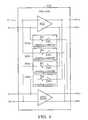
- FIG. 4shows an embodiment of a shared filter module 400 according to the current disclosure.
- the shared filter module 400is an enhanced version of the shared filter module 210 , in which the LPFs 302 I and 302 Q are substituted by a compound filter 410 comprising two LPFs 402 I and 402 Q, and a coupling controller 404 .
- the LPFs 402 I and 402 Qare typically identical to the LPFs 302 I and 302 Q.
- the coupling controller 404further provides a mode dependent coupling function to render different performance.
- the input and output ends of the LPFs 402 I and 402 Q(shown as the node finI, foutI, finQ and foutQ) are wired with the coupling controller 404 .
- the coupling controller 404When the shared filter module 400 operates in transmission mode, the coupling controller 404 is disabled, thus making the LPFs 402 I and 402 Q act as ordinary LPFs 302 I and 302 Q. While in receiver mode, however, the coupling controller 404 is enabled to couple the node finI to the node foutQ, and the node finQ to the node foutI. In this way, a cross coupling structure is established, and as a result, the compound filter 410 acts as a bandpass filter.
- the enhancement of compound filter 410provides a cost effective transceiver combining a low intermediate frequency (LIF) receiver with a direct conversion (ZIF) transmitter.
- LIFlow intermediate frequency
- ZIFdirect conversion
- the passband of compound filter 410can be effectively adjusted by tuning the time constants of LPFs 402 I and 402 Q using the calibration unit 330 . Therefore, any bandwidth requirement can be flexibly satisfied.
- the transmittercan also be a LIF transmitter, and the receiver can also be a ZIF receiver. Combination of the operation modes is not limited, benefiting from not only cost reduction but also flexibility for wide applications.
- FIG. 5shows an alternative embodiment of the compound filter 410 in FIG. 4 .
- the compound filter 410is a ladder structure comprising a plurality of filter cells 510 cascaded in series.
- Each filter cell 510comprises two LPFs 402 I and 402 Q, and a coupling controller 404 .
- the input and output nodes of the LPF 402 Iare P 1 and P 2
- the input and output nodes of the quadrature low pass filter 402 Qare P 3 and P 4 .
- the coupling controller 404specifically comprises a first coupling controller 502 and a first coupling controller 502 .
- the first coupling controller 502masters the conductivity between the nodes P 1 and P 4
- the second coupling controller 504controls that of the nodes P 2 and P 3 .
- a total of LPFs 402 Iform a third order low pass filter starting at node finI and ending at node foutI
- a total of LPFs 402 Qanother third order low pass filter starting at node finQ and ending at node foutQ.
- the first coupling controller 502 and second coupling controller 504are enabled to connect their associated ends, such that the compound filter 410 acts as a bandpass filter to pass a predetermined band, and the transceiving system 200 physically acts a LIF receiver.
- the first coupling controller 502 and second coupling controller 504are disabled, and the LPFs 402 I and 402 Q form two individual low pass filters, making the transceiving system 200 a direct conversion transmitter.
- the LPFs 402 I and 402 Qmay be designed with bandwidths of 1.5 Mhz with center frequency 1.6 Mhz. It is noted that although not shown in FIG. 5 , a preferred embodiment based on FIG. 5 may also use a calibration unit 330 to flexibly calibrate bandwidths of the LPFs 402 I and 402 Q to meet specific requirements.
- FIG. 6shows an embodiment of a filter cell 510 according to FIG. 5 .
- the LPF 402 I or 402 Qcomprises an operational amplifier (OPA) 602 I or 602 Q with parameter dependent RC circuits (not shown).
- OPAoperational amplifier
- the input and output ends of the OPAs 602 I and 602 Qare differential channels marked as P 1 +, P 1 ⁇ , P 2 +, P 2 ⁇ , P 3 +, P 3 ⁇ , P 4 + and P 4 ⁇ .
- P 2 + and P 2 ⁇ of a former OPA 602 Iare respectively coupled to the P 1 + and P 1 ⁇ of a successive OPA 602 I.
- Each coupling controllercomprises a resistor and a switch.
- the resistorsare Ra, Rb, Rc and Rd respectively, and the switches are SW 1 , SW 2 , SW 3 and SW 4 .
- the first coupling controller 502 acouples P 1 ⁇ to P 4 ⁇
- the second coupling controller 502 bcouples P 1 + to P 4 +
- the third coupling controller 504 acouples P 2 + to P 3 +
- the fourth coupling controller 504 bcouples P 2 ⁇ to P 3 ⁇ .
- the switchesare synchronously turned on or off in this embodiment.
- the filter cell 510acts as a bandpass filter having bandwidth determinable by the RC time constants.
- the OPAs 602 I and 602 Qact as ordinary LPFs to pass a specific band determined by the RC time constants.
- the resistors Ra, Rb, Rc and Rdare selectable values depending on the application.
Landscapes
- Engineering & Computer Science (AREA)
- Computer Networks & Wireless Communication (AREA)
- Signal Processing (AREA)
- Transceivers (AREA)
Abstract
Description
Claims (21)
Priority Applications (1)
| Application Number | Priority Date | Filing Date | Title |
|---|---|---|---|
| US11/853,072US7982533B2 (en) | 2005-08-22 | 2007-09-11 | Transceiving system and compound filter |
Applications Claiming Priority (3)
| Application Number | Priority Date | Filing Date | Title |
|---|---|---|---|
| US11/209,912US20070040605A1 (en) | 2005-08-22 | 2005-08-22 | Shared receiver and transmitter filter |
| US82622206P | 2006-09-20 | 2006-09-20 | |
| US11/853,072US7982533B2 (en) | 2005-08-22 | 2007-09-11 | Transceiving system and compound filter |
Related Parent Applications (1)
| Application Number | Title | Priority Date | Filing Date |
|---|---|---|---|
| US11/209,912Continuation-In-PartUS20070040605A1 (en) | 2005-08-22 | 2005-08-22 | Shared receiver and transmitter filter |
Publications (2)
| Publication Number | Publication Date |
|---|---|
| US20080002597A1 US20080002597A1 (en) | 2008-01-03 |
| US7982533B2true US7982533B2 (en) | 2011-07-19 |
Family
ID=38876533
Family Applications (1)
| Application Number | Title | Priority Date | Filing Date |
|---|---|---|---|
| US11/853,072Active2028-04-20US7982533B2 (en) | 2005-08-22 | 2007-09-11 | Transceiving system and compound filter |
Country Status (1)
| Country | Link |
|---|---|
| US (1) | US7982533B2 (en) |
Cited By (5)
| Publication number | Priority date | Publication date | Assignee | Title |
|---|---|---|---|---|
| US20100309827A1 (en)* | 2008-02-20 | 2010-12-09 | Samsung Electronics Co., Ltd. | Method and apparatus for processing signals at time division duplex transceiver |
| US20110021162A1 (en)* | 2009-07-16 | 2011-01-27 | Samsung Electronics Co., Ltd. | System for transmitting/receiving multi-band radio frequency signal using dual input, dual output filter |
| US8670741B2 (en)* | 2011-12-21 | 2014-03-11 | Triquint Semiconductor, Inc. | Mixer with high second-order and third-order intercept point |
| US20160134258A1 (en)* | 2012-10-09 | 2016-05-12 | Microchip Technology Incorporated | Switchable Filtering Circuit And The Operation Method Using The Same |
| US10587303B2 (en)* | 2018-07-30 | 2020-03-10 | Realtek Semiconductor Corp. | Transceiver control circuit for reducing operating mode transition period of transceiver |
Families Citing this family (6)
| Publication number | Priority date | Publication date | Assignee | Title |
|---|---|---|---|---|
| US8264387B2 (en)* | 2006-03-31 | 2012-09-11 | Silicon Laboratories Inc. | Transceiver having multiple signal processing modes of operation |
| JP5108325B2 (en)* | 2007-02-15 | 2012-12-26 | 富士通株式会社 | Signal processing apparatus and correction method thereof |
| JP5393607B2 (en)* | 2010-07-15 | 2014-01-22 | パナソニック株式会社 | Direct sampling circuit |
| US8768994B2 (en)* | 2010-10-22 | 2014-07-01 | Taiwan Semiconductor Manufacturing Company, Ltd. | Filter auto-calibration using multi-clock generator |
| US9419674B2 (en)* | 2013-02-26 | 2016-08-16 | Qualcomm Incorporated | Shared filter for transmit and receive paths |
| US12176939B2 (en)* | 2021-05-19 | 2024-12-24 | Qualcomm Incorporated | System and method for sharing circuitry between transmit and receive path |
Citations (16)
| Publication number | Priority date | Publication date | Assignee | Title |
|---|---|---|---|---|
| US4501018A (en)* | 1983-07-05 | 1985-02-19 | Motorola, Inc. | Simplex transceiver employing a common piezoelectric element for transmitting and receiving |
| US5694419A (en) | 1995-11-07 | 1997-12-02 | Hitachi America, Ltd. | Shared resource modulator-demodulator circuits for use with vestigial sideband signals |
| CN1328723A (en) | 1998-11-26 | 2001-12-26 | 诺基亚移动电话有限公司 | Method and arrangement for transmitting and receiving RF signals through various radio interfaces of communication systems |
| US6377788B1 (en) | 1997-05-09 | 2002-04-23 | Micrel, Incorporated | Tunable filter in radio receiver |
| US6466613B1 (en)* | 1999-04-26 | 2002-10-15 | Itran Communications Ltd. | Communications transceiver utilizing a single filter |
| US6657483B1 (en) | 2002-11-25 | 2003-12-02 | Texas Instruments Incorporated | Adjusting the trans-conductance of a filter |
| US6728517B2 (en)* | 2002-04-22 | 2004-04-27 | Cognio, Inc. | Multiple-input multiple-output radio transceiver |
| US6803813B1 (en) | 2003-04-22 | 2004-10-12 | National Semiconductor Corporation | Time constant-based calibration circuit for active filters |
| US20050048928A1 (en) | 2003-08-28 | 2005-03-03 | Young-Deuk Jeon | System and method for filtering signals in a transceiver |
| US6891414B1 (en) | 2004-03-05 | 2005-05-10 | Rf Micro Devices, Inc. | Digital calibration for capacitor voltage non-linearity |
| CN1677882A (en) | 2004-04-02 | 2005-10-05 | 大唐移动通信设备有限公司 | Message machine of receiving-transmitting time-division duplex wireless communication system |
| US6993310B2 (en) | 2002-08-30 | 2006-01-31 | Microtune (Texas), L.P. | Current driven polyphase filters and method of operation |
| US7031669B2 (en)* | 2002-09-10 | 2006-04-18 | Cognio, Inc. | Techniques for correcting for phase and amplitude offsets in a MIMO radio device |
| US7116159B2 (en) | 2001-05-03 | 2006-10-03 | Infineon Technologies Ag | Method and apparatus for adjusting an active filter |
| US7463864B2 (en)* | 2004-04-09 | 2008-12-09 | Broadcom Corporation | Modified dual band direct conversion architecture that allows extensive digital calibration |
| US7636554B2 (en)* | 2002-04-22 | 2009-12-22 | Ipr Licensing, Inc. | Multiple-input multiple-output radio transceiver |
- 2007
- 2007-09-11USUS11/853,072patent/US7982533B2/enactiveActive
Patent Citations (16)
| Publication number | Priority date | Publication date | Assignee | Title |
|---|---|---|---|---|
| US4501018A (en)* | 1983-07-05 | 1985-02-19 | Motorola, Inc. | Simplex transceiver employing a common piezoelectric element for transmitting and receiving |
| US5694419A (en) | 1995-11-07 | 1997-12-02 | Hitachi America, Ltd. | Shared resource modulator-demodulator circuits for use with vestigial sideband signals |
| US6377788B1 (en) | 1997-05-09 | 2002-04-23 | Micrel, Incorporated | Tunable filter in radio receiver |
| CN1328723A (en) | 1998-11-26 | 2001-12-26 | 诺基亚移动电话有限公司 | Method and arrangement for transmitting and receiving RF signals through various radio interfaces of communication systems |
| US6466613B1 (en)* | 1999-04-26 | 2002-10-15 | Itran Communications Ltd. | Communications transceiver utilizing a single filter |
| US7116159B2 (en) | 2001-05-03 | 2006-10-03 | Infineon Technologies Ag | Method and apparatus for adjusting an active filter |
| US7636554B2 (en)* | 2002-04-22 | 2009-12-22 | Ipr Licensing, Inc. | Multiple-input multiple-output radio transceiver |
| US6728517B2 (en)* | 2002-04-22 | 2004-04-27 | Cognio, Inc. | Multiple-input multiple-output radio transceiver |
| US6993310B2 (en) | 2002-08-30 | 2006-01-31 | Microtune (Texas), L.P. | Current driven polyphase filters and method of operation |
| US7031669B2 (en)* | 2002-09-10 | 2006-04-18 | Cognio, Inc. | Techniques for correcting for phase and amplitude offsets in a MIMO radio device |
| US6657483B1 (en) | 2002-11-25 | 2003-12-02 | Texas Instruments Incorporated | Adjusting the trans-conductance of a filter |
| US6803813B1 (en) | 2003-04-22 | 2004-10-12 | National Semiconductor Corporation | Time constant-based calibration circuit for active filters |
| US20050048928A1 (en) | 2003-08-28 | 2005-03-03 | Young-Deuk Jeon | System and method for filtering signals in a transceiver |
| US6891414B1 (en) | 2004-03-05 | 2005-05-10 | Rf Micro Devices, Inc. | Digital calibration for capacitor voltage non-linearity |
| CN1677882A (en) | 2004-04-02 | 2005-10-05 | 大唐移动通信设备有限公司 | Message machine of receiving-transmitting time-division duplex wireless communication system |
| US7463864B2 (en)* | 2004-04-09 | 2008-12-09 | Broadcom Corporation | Modified dual band direct conversion architecture that allows extensive digital calibration |
Non-Patent Citations (3)
| Title |
|---|
| "An Integrated 52GHz CMOS T/R Switch with LC-tuned Substrate Bias" Talwalkar, et al., 2003. |
| English language translation of abstract of CN 1328723 (published Dec. 26, 2001). |
| English language translation of abstract of CN 1677882 (published Oct. 5, 2005). |
Cited By (9)
| Publication number | Priority date | Publication date | Assignee | Title |
|---|---|---|---|---|
| US20100309827A1 (en)* | 2008-02-20 | 2010-12-09 | Samsung Electronics Co., Ltd. | Method and apparatus for processing signals at time division duplex transceiver |
| US9331736B2 (en)* | 2008-02-20 | 2016-05-03 | Samsung Electronics Co., Ltd. | Method and apparatus for processing signals at time division duplex transceiver |
| US20110021162A1 (en)* | 2009-07-16 | 2011-01-27 | Samsung Electronics Co., Ltd. | System for transmitting/receiving multi-band radio frequency signal using dual input, dual output filter |
| US8918063B2 (en)* | 2009-07-16 | 2014-12-23 | Samsung Electronics Co., Ltd. | System for transmitting/receiving multi-band radio frequency signal using dual input, dual output filter |
| US8670741B2 (en)* | 2011-12-21 | 2014-03-11 | Triquint Semiconductor, Inc. | Mixer with high second-order and third-order intercept point |
| TWI565226B (en)* | 2011-12-21 | 2017-01-01 | 三胞半導體公司 | Mixer with high second-order and third-order intercept point |
| US20160134258A1 (en)* | 2012-10-09 | 2016-05-12 | Microchip Technology Incorporated | Switchable Filtering Circuit And The Operation Method Using The Same |
| US10009060B2 (en)* | 2012-10-09 | 2018-06-26 | Microchip Technology Incorporated | Switchable filtering circuit and the operation method using the same |
| US10587303B2 (en)* | 2018-07-30 | 2020-03-10 | Realtek Semiconductor Corp. | Transceiver control circuit for reducing operating mode transition period of transceiver |
Also Published As
| Publication number | Publication date |
|---|---|
| US20080002597A1 (en) | 2008-01-03 |
Similar Documents
| Publication | Publication Date | Title |
|---|---|---|
| US7982533B2 (en) | Transceiving system and compound filter | |
| US7231189B2 (en) | Transmit and/or receive channel communication system with switchably coupled multiple filtering components | |
| US7395040B2 (en) | Multiple band multiple input multiple output transceiver integrated circuit | |
| EP2244376B1 (en) | Cascode CMOS RF power amplifier with programmable feedback cascode bias under multiple supply voltages | |
| EP2557696B1 (en) | Multiple-input multiple-output radio transceiver | |
| US7636554B2 (en) | Multiple-input multiple-output radio transceiver | |
| US7787843B2 (en) | Multiple band direct conversion radio frequency transceiver integrated circuit | |
| US8923777B2 (en) | Low-IF transceiver architecture | |
| EP1522151B1 (en) | System and method for a direct conversion multi-carrier processor | |
| JP2002543658A (en) | System and process for shared function block CDMA / GSM communication transceiver | |
| EP1811678A2 (en) | Radio frequency signal transmission/reception apparatus and radio frequency signal transmission/reception method | |
| JP2007504717A (en) | System and method for filtering signals in a transceiver | |
| US20060286939A1 (en) | Local signal generation circuit | |
| CN105409177A (en) | Analog baseband filter device and control method for multimode multiband wireless transceiver | |
| JP4757214B2 (en) | Filter circuit | |
| US20080218256A1 (en) | Channel Filtering in Radio Communications Systems | |
| JP3934162B2 (en) | Equipment in a communication system | |
| JP3816356B2 (en) | Wireless transmitter | |
| CN101150328B (en) | Transceiver system and combined filter | |
| US6807237B1 (en) | Radio apparatus and transmission/reception method | |
| CN111130747B (en) | Wideband receiver compatible with voice channel | |
| US12308869B2 (en) | Phase-reconfigurable circuits with programmable power splitting for dual-input power amplifiers | |
| JP2004357025A (en) | Receiving machine | |
| HK1118397A1 (en) | Multiple-input multiple-output radio transceiver | |
| HK1118397B (en) | Multiple-input multiple-output radio transceiver |
Legal Events
| Date | Code | Title | Description |
|---|---|---|---|
| AS | Assignment | Owner name:CRYSTALMEDIA TECHNOLOGY, INC., CALIFORNIA Free format text:ASSIGNMENT OF ASSIGNORS INTEREST;ASSIGNORS:FAN, YIPING;CHAO, CHIEH-YUAN;REEL/FRAME:019806/0893;SIGNING DATES FROM 20070731 TO 20070801 Owner name:CRYSTALMEDIA TECHNOLOGY, INC., CALIFORNIA Free format text:ASSIGNMENT OF ASSIGNORS INTEREST;ASSIGNORS:FAN, YIPING;CHAO, CHIEH-YUAN;SIGNING DATES FROM 20070731 TO 20070801;REEL/FRAME:019806/0893 | |
| AS | Assignment | Owner name:MEDIATEK USA INC., CALIFORNIA Free format text:CHANGE OF NAME;ASSIGNOR:CRYSTALMEDIA TECHNOLOGY, INC.;REEL/FRAME:020381/0740 Effective date:20080103 Owner name:MEDIATEK USA INC.,CALIFORNIA Free format text:CHANGE OF NAME;ASSIGNOR:CRYSTALMEDIA TECHNOLOGY, INC.;REEL/FRAME:020381/0740 Effective date:20080103 | |
| STCF | Information on status: patent grant | Free format text:PATENTED CASE | |
| FPAY | Fee payment | Year of fee payment:4 | |
| MAFP | Maintenance fee payment | Free format text:PAYMENT OF MAINTENANCE FEE, 8TH YEAR, LARGE ENTITY (ORIGINAL EVENT CODE: M1552); ENTITY STATUS OF PATENT OWNER: LARGE ENTITY Year of fee payment:8 | |
| MAFP | Maintenance fee payment | Free format text:PAYMENT OF MAINTENANCE FEE, 12TH YEAR, LARGE ENTITY (ORIGINAL EVENT CODE: M1553); ENTITY STATUS OF PATENT OWNER: LARGE ENTITY Year of fee payment:12 |