US7978802B1 - Method and apparatus for a mesochronous transmission system - Google Patents
Method and apparatus for a mesochronous transmission systemDownload PDFInfo
- Publication number
- US7978802B1 US7978802B1US11/974,362US97436207AUS7978802B1US 7978802 B1US7978802 B1US 7978802B1US 97436207 AUS97436207 AUS 97436207AUS 7978802 B1US7978802 B1US 7978802B1
- Authority
- US
- United States
- Prior art keywords
- clock signal
- phase
- coupled
- bit clock
- receive
- Prior art date
- Legal status (The legal status is an assumption and is not a legal conclusion. Google has not performed a legal analysis and makes no representation as to the accuracy of the status listed.)
- Active, expires
Links
- 230000005540biological transmissionEffects0.000titleclaimsabstractdescription45
- 238000000034methodMethods0.000titleabstractdescription7
- 239000004744fabricSubstances0.000claimsdescription55
- 230000004044responseEffects0.000claimsdescription18
- 239000000872bufferSubstances0.000claimsdescription6
- 230000001360synchronised effectEffects0.000abstractdescription4
- 238000004891communicationMethods0.000description14
- 229920002319Poly(methyl acrylate)Polymers0.000description13
- 201000008752progressive muscular atrophyDiseases0.000description13
- 238000010586diagramMethods0.000description4
- 230000001427coherent effectEffects0.000description3
- 238000012545processingMethods0.000description3
- 230000008859changeEffects0.000description2
- 230000009467reductionEffects0.000description2
- 238000010420art techniqueMethods0.000description1
- 230000003139buffering effectEffects0.000description1
- 238000011161developmentMethods0.000description1
- 230000018109developmental processEffects0.000description1
- 230000001747exhibiting effectEffects0.000description1
- 230000006870functionEffects0.000description1
- 238000013508migrationMethods0.000description1
- 230000005012migrationEffects0.000description1
- 230000008450motivationEffects0.000description1
- 238000005191phase separationMethods0.000description1
- 238000011084recoveryMethods0.000description1
- 238000012552reviewMethods0.000description1
- 238000012546transferMethods0.000description1
Images


Classifications
- H—ELECTRICITY
- H04—ELECTRIC COMMUNICATION TECHNIQUE
- H04L—TRANSMISSION OF DIGITAL INFORMATION, e.g. TELEGRAPHIC COMMUNICATION
- H04L7/00—Arrangements for synchronising receiver with transmitter
- H04L7/0016—Arrangements for synchronising receiver with transmitter correction of synchronization errors
- H04L7/002—Arrangements for synchronising receiver with transmitter correction of synchronization errors correction by interpolation
- H04L7/0025—Arrangements for synchronising receiver with transmitter correction of synchronization errors correction by interpolation interpolation of clock signal
- H—ELECTRICITY
- H03—ELECTRONIC CIRCUITRY
- H03L—AUTOMATIC CONTROL, STARTING, SYNCHRONISATION OR STABILISATION OF GENERATORS OF ELECTRONIC OSCILLATIONS OR PULSES
- H03L7/00—Automatic control of frequency or phase; Synchronisation
- H03L7/06—Automatic control of frequency or phase; Synchronisation using a reference signal applied to a frequency- or phase-locked loop
- H03L7/07—Automatic control of frequency or phase; Synchronisation using a reference signal applied to a frequency- or phase-locked loop using several loops, e.g. for redundant clock signal generation
- H—ELECTRICITY
- H03—ELECTRONIC CIRCUITRY
- H03L—AUTOMATIC CONTROL, STARTING, SYNCHRONISATION OR STABILISATION OF GENERATORS OF ELECTRONIC OSCILLATIONS OR PULSES
- H03L7/00—Automatic control of frequency or phase; Synchronisation
- H03L7/06—Automatic control of frequency or phase; Synchronisation using a reference signal applied to a frequency- or phase-locked loop
- H03L7/08—Details of the phase-locked loop
- H03L7/081—Details of the phase-locked loop provided with an additional controlled phase shifter
- H—ELECTRICITY
- H03—ELECTRONIC CIRCUITRY
- H03L—AUTOMATIC CONTROL, STARTING, SYNCHRONISATION OR STABILISATION OF GENERATORS OF ELECTRONIC OSCILLATIONS OR PULSES
- H03L7/00—Automatic control of frequency or phase; Synchronisation
- H03L7/06—Automatic control of frequency or phase; Synchronisation using a reference signal applied to a frequency- or phase-locked loop
- H03L7/08—Details of the phase-locked loop
- H03L7/085—Details of the phase-locked loop concerning mainly the frequency- or phase-detection arrangement including the filtering or amplification of its output signal
- H03L7/087—Details of the phase-locked loop concerning mainly the frequency- or phase-detection arrangement including the filtering or amplification of its output signal using at least two phase detectors or a frequency and phase detector in the loop
- H—ELECTRICITY
- H04—ELECTRIC COMMUNICATION TECHNIQUE
- H04L—TRANSMISSION OF DIGITAL INFORMATION, e.g. TELEGRAPHIC COMMUNICATION
- H04L7/00—Arrangements for synchronising receiver with transmitter
- H04L7/02—Speed or phase control by the received code signals, the signals containing no special synchronisation information
- H04L7/033—Speed or phase control by the received code signals, the signals containing no special synchronisation information using the transitions of the received signal to control the phase of the synchronising-signal-generating means, e.g. using a phase-locked loop
- H04L7/0331—Speed or phase control by the received code signals, the signals containing no special synchronisation information using the transitions of the received signal to control the phase of the synchronising-signal-generating means, e.g. using a phase-locked loop with a digital phase-locked loop [PLL] processing binary samples, e.g. add/subtract logic for correction of receiver clock
Definitions
- the present inventiongenerally relates to gigabit serial transmitters, and more particularly to reduced lane-lane skew in multiple channel transmission systems.
- Serial I/O solutionswill most probably be deployed in nearly every electronic product imaginable, including IC-to-IC interfacing, backplane connectivity, and box-to-box communications.
- PCIePCI-Express
- UIunit intervals
- Prior art methods that reduce the lane-lane skew for multiple channel communication buseshave focused on aligning the serial transmitter at the byte level, using multiple phase alignment modules in the physical coding sublayer (PCS) and associated processing at the higher link transaction layers.
- Other prior art methods to reduce the lane-lane skew for multiple channel communication buseshave focused on aligning the serial transmitter at the bit level through the use of a barrel shifter.
- Prior art lane-lane skew reduction techniquesthat are combined with techniques to provide low latency modes of operation, however, tend to degrade each other's performance.
- prior art techniques to obtain low latency modes of operationprovide data paths that bypass those transmission circuit components that are sources of latency, such as elastic buffers or first-in, first-out (FIFO) buffers.
- FIFOfirst-in, first-out
- providing data bypass pathsoften involves the traversal of 2 or more clock domains.
- timing problemsare also generated, since the timing relationships between the bypass data paths and all traversed clock domains may no longer be guaranteed.
- various embodiments of the present inventiondisclose an apparatus and method for a mesochronous transmission system that reduces lane-lane skew in multiple channel communication buses, provides a low latency mode of operation, and provides reliable data propagation across all clock domains.
- an integrated circuitcomprises a configurable logic fabric that is coupled to receive configuration data.
- the configurable logic fabricincludes programmable logic devices and programmable interconnections that are configured to provide data in response to a fabric clock signal, the fabric clock signal being derived from a reference clock signal.
- the ICfurther comprises a master transmitter that is coupled to the configurable logic fabric and is adapted to receive the data from the configurable logic fabric in response to a first byte clock signal and is adapted to transmit the data in response to a first bit clock signal.
- the master transmitterincludes a first phase locked loop (PLL) that is adapted to generate the first bit clock signal in phase coherency with the reference clock signal and a first phase alignment block that is coupled to the first PLL and is adapted to generate the first byte clock signal in phase coherency with the fabric clock signal.
- PLLphase locked loop
- a programmable logic devicecomprises a configurable logic fabric that is adapted to provide data for transmission from the PLD, a plurality of transceivers configured to receive the data and adapted to provide a multiple channel transmission bus to transmit the data.
- Each of the transceiversinclude a physical coding sublayer (PCS) that is coupled to receive the data into an input register in synchronization with a first clock signal provided by the configurable logic fabric.
- the PCSincludes an elastic buffer programmably decoupled from an output of the input register in a first mode.
- Each of the transceiversfurther include a physical media access (PMA) block that is adapted to receive the data from an output register of the PCS in synchronization with a second clock signal derived by the PMA block.
- the output registeris programmably coupled to the input register to bypass the elastic buffer in the first mode.
- the PMA blockmaintains the second clock signal in phase alignment with the first clock signal in the first mode.
- a transmission systemcomprises a first transmitter that is coupled to transmit data to a transmission medium.
- the first transmitterincludes a configurable logic fabric that is coupled to receive configuration data to configure programmable logic devices and programmable interconnections within the configurable logic fabric to provide the data in synchronization with a fabric clock signal.
- the first transmitterfurther includes a physical coding sublayer (PCS) that is coupled to receive the data into an input register in synchronization with the fabric clock signal provided by the configurable logic fabric.
- the first transmitterfurther includes a physical media access (PMA) block that is adapted to receive the data from an output register of the PCS in synchronization with a byte clock signal provided by the PMA block. The PMA block maintains the byte clock signal in phase alignment with the fabric clock signal.
- PCSphysical coding sublayer
- PMAphysical media access
- FIG. 1illustrates exemplary communication stacks for the various PHY layers of a gigabit transceiver
- FIG. 2illustrates an exemplary block diagram of a multiple channel transmission bus
- FIG. 3illustrates an exemplary block diagram of the phase locked loop and phase alignment block portions of the multiple channel transmission bus of FIG. 2 ;
- FIG. 4illustrates an alternate block diagram of the exemplary phase locked loop and phase alignment block portions of the multiple channel transmission bus of FIG. 2 .
- the various embodiments of the present inventionare applied to a multiple lane transmission system that provides both a low latency mode of operation, while at the same time, provides reduced lane-lane skew.
- the overall transmission systemoperates as a mesochronous system, whereby each clock domain of the transmission system is synchronized to the leaf nodes of a global clock tree.
- Synchronization of the transmission systemis performed by achieving phase/frequency lock to a local reference.
- the frequency of the local referenceis multiplied by a phase locked loop (PLL) to generate both a bit clock and a byte clock.
- the bit clockis the high speed clock, which operates at approximately half of the serial data rate for double data rate (DDR) applications and operates at the serial data rate for other applications.
- the byte clockis the lower frequency clock that operates at data byte boundaries, where for example, the number of bits, n, for each data byte may be equal to 8 or 10 bits per byte.
- Both the bit clock and the byte clockare phase coherent with respect to one another and are used by the serializer/deserializer (SERDES) to provide the parallel to serial operations.
- SERDESserializer/deserializer
- the reference clockis then routed to the core of the integrated circuit (IC) to provide the timing reference to the root of a global clock tree.
- Secondary circuits in the FPGAsuch as an optional PLL, may be used to multiply the reference clock up to a higher frequency, such as the frequency of signal byte clock, if required.
- the leaf nodes of the global clock treeare then fanned out throughout all clock domains of the physical media attachment (PMA) layers and physical coding sublayers (PCS) of the transmission system.
- PMAphysical media attachment
- PCSphysical coding sublayers
- phase alignment blockis then used to align the phase of both the bit and byte clock signals to the clock signal generated at the leaf nodes of the global clock tree.
- a phase interpolatoris added to the feedback path of the phase locked loop. The exact phase of the phase interpolator is controlled by a phase detector in response to a phase error that is measured between the phase of the clock signal at the leaf node and the phase of the byte clock that is generated by the PLL.
- the phase detectorthen generates an up/down command to a finite state machine (FSM), which in turn generates a digital control word to the phase interpolator that is effective to substantially remove the phase error.
- FSMfinite state machine
- the overall loopsettles when the phase of the bit and byte clocks are aligned with the phase of the clock signal generated at the leaf nodes of the global clock tree.
- phase interpolatoris utilized outside of the feedback path of the PLL.
- a synchronization operationis required to be executed at regular intervals to minimize the amount of phase error between the byte clock and the clock signal at the leaf nodes of the global clock tree.
- Both embodimentsmay be enabled through the configuration of the programmable logic fabric of a programmable logic device (PLD) such as a field programmable gate array (FPGA).
- PLDprogrammable logic device
- FPGAfield programmable gate array
- features of each embodimentmay instead be enabled through a partial reconfiguration of the PLD.
- the timing relationship between the programmable logic fabric and each transmission channelis based upon the phase of the clock that is utilized within the programmable logic fabric, i.e., the clock generated by the global clock tree.
- the entire transmit clock domain of the transceivermay, therefore, be shifted in phase coherency with the global clock tree.
- Such an arrangementallows the phase alignment to be performed within the PLL block of the transceiver, which maximizes the setup and hold margins.
- the arrangementfurther allows a reset command to be generated from a configuration module within the programmable logic fabric, which may then be used to synchronize two or more transmission lanes within the PMA portion of the transmitter.
- a configuration module within the programmable logic fabricwhich may then be used to synchronize two or more transmission lanes within the PMA portion of the transmitter.
- FIG. 1an exemplary communication stack is illustrated, whereby PHY layers 112 - 116 are implemented within a PLD such as an FPGA.
- PLDsuch as an FPGA
- the associated PMA and PCS layersmay reside within a gigabit transceiver of the FPGA
- the media access layer (MAC) and the higher link transaction layersmay reside within the programmable logic portion, i.e., programmable fabric and associated processing 102 , that also resides within the FPGA.
- MACmedia access layer
- PHY layer 112may represent a PHY interface for a single gigabit transceiver, while PHY layers 114 and 116 of the FPGA may be simultaneously configured for other communication protocols.
- all of the TX interfaces of PHY layers 112 - 116may be combined to form a multiple channel transmission bus that is PCIe compliant, thereby exhibiting reduced lane-lane skew in a low latency mode of operation.
- PMA 110 , 120 , and 124provide a SERDES function, whereby parallel data received from PCS 108 , 118 , and 122 , respectively, may be serialized prior to transmission via the TX interface. Further, serial data received from the RX interface may be converted to parallel data prior to being delivered to PCS 108 , 118 , and 122 .
- PMA 110 , 120 , and 124may also incorporate a clock and data recovery (CDR) module whereby a clock signal and a data signal is derived from the input signal received at the RX interface. Once derived, the clock signal may be divided to form a parallel clock signal that is used to propagate the parallel data into the FPGA for further processing.
- CDRclock and data recovery
- only one PMA of PMAs 110 , 120 , and 124is considered to be the master PMA, whereby the master PMA transmits the reference clock that is used to drive the root of the global clock tree (not shown) existing within programmable logic fabric 102 .
- Clock signals from the leaf nodes of the global clock treemay then be fanned out to the remaining slave PMAs, whereby the slave PMAs phase align their respective transmission drivers to the reference clock signal that is received from their respective global clock tree leaf nodes.
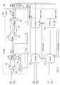
- FIG. 2an exemplary block diagram of a multiple channel, transmission system 220 is illustrated, whereby transmission PMA (TX-PMA) 202 is illustrated as the master PMA, while TX-PMAs 236 and 240 are illustrated as the slave PMAs.
- TX-PMA 202is tasked with transmitting the reference clock signal to global clock tree 232 for dissemination by the leaf nodes of global clock tree 232 .
- TX-PMA 202coherently multiplies the reference clock signal received from REF CLK 206 through the use of PLL 216 .
- TX-PMA 202is simultaneously tasked with phase aligning the byte clock that is generated by PLL 216 to the clock signal that is generated by global clock tree 232 .
- synchronization of all channels of the transmission system of FIG. 2is performed by first achieving phase/frequency lock to a local reference, e.g., REF CLK 206 , and multiplying the frequency reference up to a frequency that is equal to the clock signal, i.e., byte clock, that is used to read data words from output data register 244 during a bypass mode of operation.
- the REF CLK 206is also provided to the root of global clock tree 232 , with or without multiplication, based on the relationship between REF CLK and byte clock.
- a multipliersuch as PLL 246 , may be used to multiply REF CLK to a frequency that is substantially equal to byte clock. Subsequent distribution from the leaf nodes of global clock tree 232 , to TX-PCS 204 , 234 , and 238 and to TX-PMA 202 , 236 , and 240 is then performed.
- PLL 216also generates a bit clock that is phase coherent with the byte clock.
- the bit clockis the high speed clock, which operates at approximately half of the serial data rate for double data rate (DDR) applications and operates at the serial data rate for other applications.
- DDRdouble data rate
- Phase alignment block 214is then utilized to phase align the bit and byte clocks to the byte clock signal that is distributed by the leaf nodes of global clock tree 232 .
- the bit clockis then provided to a serializer (not shown) within TX-PMA 202 , which serializes the parallel data coming from TX-PCS 204 prior to transmission by TX DRVR 208 via terminals TX p and TX N .
- multiplexers 222 and 226 of TX-PCS 204are provided to allow bypassing of FIFO 224 and/or 8 B/ 10 B coding block 228 , respectively, when a low latency mode of operation is desired.
- the elastic buffering operation performed by FIFO 224is also bypassed.
- the clock signals provided to input data register 242 and output data register 244must be in a known phase relationship with respect to one another in order to facilitate reliable data transfer.
- Phase alignment block 214is, therefore, activated during bypass mode to insure that such a phase relationship exists. That is to say, in other words, that while global clock tree 232 provides the byte clock that is required to clock data bytes into input register 242 , the phase aligned byte clock from phase alignment block 214 is used to clock data words out of output register 244 . Given that phase alignment block 214 insures that the byte clock distributed by global clock tree 232 is phase aligned with the byte clock delivered by phase alignment block 214 , reliable data propagation through TX-PCS 204 is guaranteed.
- phase alignment block 214 and PLL 216 of TX-PMA 202seeks to maintain a coherent phase relationship between signal REF CLK and the bit clock that is provided by VCO 306 to Divide-by-N interger divider 316 and serializer 314 .
- PLL 216includes phase frequency detector (PFD) 302 to compare the phase/frequency of signal REF CLK to a divided version of the phase/frequency of the output of voltage controlled oscillator (VCO) 306 , f VCO /P.
- PFDphase frequency detector
- phase and/or frequency error that is detected between signal REF CLK and f VCO /P by PFD 302is converted into an error signal and subsequently provided to loop filter 304 .
- Loop filter 304integrates the phase and/or frequency error to generate an error voltage, which is then provided to VCO 306 .
- VCO 306adjusts its output frequency, f VCO , such that the phase/frequency error between signal REF CLK and signal f VCO is minimized.
- interpolator 308Integrated within the feedback path of PLL 216 is interpolator 308 , which is configured to receive several outputs from VCO 306 .
- VCO 306provides several phase variants of signal f VCO to interpolator 308 , whereby a first variant is signal f VCO itself, a second variant exhibits a phase offset, X, from signal f VCO , a third variant exhibits a phase offset, Y, from signal f VCO and so on.
- Each of the phase variants of signal f VCO that are provided to interpolator 308exhibits an integer phase offset from signal f VCO that is inversely proportional to the number of phase variants provided. For example, given that 4 variants are provided by VCO 306 , then the first variant exhibits a 0 degree offset, the second variant exhibits a 90 degree offset, the third variant exhibits a 180 degree offset, and the fourth variant exhibits a 270 degree offset, such that 90 degree phase offsets exist between each variant.
- Interpolator 308selects the correct variant of signal f VCO from VCO 306 and in response to the control word issued by finite state machine (FSM) 320 , interpolates from the variant selected to the appropriate phase of signal f VCO that is provided to divide by P 310 , such that the phase/frequency error detected by PFD 302 is minimized.
- FSMfinite state machine
- Phase alignment block 214simultaneously seeks to maintain phase coherency between signal FABRIC CLOCK and signal BYTE CLOCK, where signal FABRIC CLOCK is received from global clock tree 232 of FIG. 2 and signal BYTE CLOCK is the timing reference provided to TX-PCS 204 from phase alignment block 214 during the bypass mode of operation as discussed above.
- Divide-by-N interger divider 316receives signal f VCO , i.e., bit clock, from VCO 306 and divides the bit clock by N to form signal BYTE CLOCK.
- divisor Nis equal to the bit length of each data word that is received from signal FABRIC DATA, which in one embodiment is equal to 8 bits per byte.
- Phase detector 318compares signal BYTE CLOCK to signal FABRIC CLOCK to generate a word clock phase error, which is then provided to FSM 320 . Based upon the word clock phase error, FSM 320 provides a binary representation that is representative of the word clock phase error to interpolator 308 .
- the binary representationmay contain 8 bits of data, such that a 256 point resolution of word clock phase error may be represented by the binary representation.
- phase alignment block 214seeks to simultaneously maintain phase coherency between signals BYTE CLOCK and FABRIC CLOCK. Any phase/frequency change that may affect signal FABRIC CLOCK, therefore, inherently creates a proportionate change in the phase/frequency of signal BYTE CLOCK.
- Signal FABRIC CLOCKis distributed to all other transmission channels of the FPGA, so that their transmitter clocks may be phase aligned to FABRIC CLOCK.
- the lane-lane skew across all transmission channels of the FPGAmay be reduced to well below 1 user interval (UI), which equates to one half of a bit clock period for DDR operation and one bit clock period for non-DDR operation.
- UIuser interval
- FSM 320provides a 256-bit resolution, for example, then the lane-lane skew from one transmission channel to the next may be reduced to within +/ ⁇ 1.4 degrees on average.
- interpolator 408does not exist within the feedback path of PLL 216 . Instead, interpolator 408 is coupled in parallel with PLL 216 to provide the interpolated BIT CLOCK signal to both serializer 414 and Divide-by-N interger divider 416 .
- the word clock phase error signal that is generated by phase detector 418 and FSM 420is not filtered by loop filter 404 and is thus subject to any clock jitter that may exist on signal FABRIC CLOCK.
- interpolator 408may be activated for a few clock cycles to obtain synchronization between signals BYTE CLOCK and FABRIC CLOCK and then deactivated until the next synchronization cycle.
Landscapes
- Engineering & Computer Science (AREA)
- Computer Networks & Wireless Communication (AREA)
- Signal Processing (AREA)
- Synchronisation In Digital Transmission Systems (AREA)
Abstract
Description
Claims (20)
Priority Applications (1)
| Application Number | Priority Date | Filing Date | Title |
|---|---|---|---|
| US11/974,362US7978802B1 (en) | 2007-10-12 | 2007-10-12 | Method and apparatus for a mesochronous transmission system |
Applications Claiming Priority (1)
| Application Number | Priority Date | Filing Date | Title |
|---|---|---|---|
| US11/974,362US7978802B1 (en) | 2007-10-12 | 2007-10-12 | Method and apparatus for a mesochronous transmission system |
Publications (1)
| Publication Number | Publication Date |
|---|---|
| US7978802B1true US7978802B1 (en) | 2011-07-12 |
Family
ID=44245594
Family Applications (1)
| Application Number | Title | Priority Date | Filing Date |
|---|---|---|---|
| US11/974,362Active2030-05-11US7978802B1 (en) | 2007-10-12 | 2007-10-12 | Method and apparatus for a mesochronous transmission system |
Country Status (1)
| Country | Link |
|---|---|
| US (1) | US7978802B1 (en) |
Cited By (16)
| Publication number | Priority date | Publication date | Assignee | Title |
|---|---|---|---|---|
| US20110191511A1 (en)* | 2010-02-02 | 2011-08-04 | Yasuhiko Tanabe | Serial transmission device, method, and computer readable medium storing program |
| US20110228889A1 (en)* | 2010-03-19 | 2011-09-22 | Dean Liu | Repeater Architecture with Single Clock Multiplier Unit |
| CN102859927A (en)* | 2012-05-10 | 2013-01-02 | 华为技术有限公司 | Data and clock recovery module and data and clock recovery method |
| US8572300B2 (en)* | 2011-10-26 | 2013-10-29 | Taiwan Semiconductor Manufacturing Co., Ltd. | Physical coding sublayer (PCS) architecture for synchronizing data between different reference clocks |
| US8850089B1 (en)* | 2010-06-18 | 2014-09-30 | Integrated Device Technology, Inc. | Method and apparatus for unified final buffer with pointer-based and page-based scheme for traffic optimization |
| US8873606B2 (en)* | 2012-11-07 | 2014-10-28 | Broadcom Corporation | Transceiver including a high latency communication channel and a low latency communication channel |
| US20150280761A1 (en)* | 2014-03-28 | 2015-10-01 | Mstar Semiconductor, Inc. | Multi-lane serial link signal receiving system |
| US9330220B1 (en)* | 2014-08-25 | 2016-05-03 | Xilinx, Inc. | Clock region partitioning and clock routing |
| US9356768B2 (en) | 2014-09-24 | 2016-05-31 | Qualcomm Incorporated | Phase detecting circuit for interchain local oscillator (LO) divider phase alignment |
| US9356769B2 (en)* | 2014-09-24 | 2016-05-31 | Qualcomm Incorporated | Synchronous reset and phase detecting for interchain local oscillator (LO) divider phase alignment |
| US9467120B1 (en)* | 2013-12-19 | 2016-10-11 | Altera Corporation | Power management for PCI express |
| US9825755B2 (en) | 2013-08-30 | 2017-11-21 | Qualcomm Incorporated | Configurable clock tree |
| US10068048B1 (en) | 2016-07-18 | 2018-09-04 | Xilinx, Inc. | Generating clock trees for a circuit design |
| US10657067B1 (en) | 2016-09-12 | 2020-05-19 | Xilinx, Inc. | Memory management unit with prefetch |
| US11101923B2 (en)* | 2017-12-27 | 2021-08-24 | Intel Corporation | Receiver circuitry for physical coding sublayer |
| CN117572312A (en)* | 2023-11-16 | 2024-02-20 | 北京大学深圳研究生院 | Ultra-high field magnetic resonance imaging equipment and ultra-high field multi-channel parallel launch system |
Citations (4)
| Publication number | Priority date | Publication date | Assignee | Title |
|---|---|---|---|---|
| US7162553B1 (en)* | 2004-10-01 | 2007-01-09 | Altera Corporation | Correlating high-speed serial interface data and FIFO status signals in programmable logic devices |
| US7317775B1 (en)* | 2004-07-16 | 2008-01-08 | National Semiconductor Corporation | Switched deskew on arbitrary data |
| US7336755B1 (en)* | 2004-06-08 | 2008-02-26 | Xilinx, Inc. | PLL with low phase noise non-integer divider |
| US7346794B1 (en)* | 2005-01-21 | 2008-03-18 | Xilinx, Inc. | Method and apparatus for providing clocking phase alignment in a transceiver system |
- 2007
- 2007-10-12USUS11/974,362patent/US7978802B1/enactiveActive
Patent Citations (4)
| Publication number | Priority date | Publication date | Assignee | Title |
|---|---|---|---|---|
| US7336755B1 (en)* | 2004-06-08 | 2008-02-26 | Xilinx, Inc. | PLL with low phase noise non-integer divider |
| US7317775B1 (en)* | 2004-07-16 | 2008-01-08 | National Semiconductor Corporation | Switched deskew on arbitrary data |
| US7162553B1 (en)* | 2004-10-01 | 2007-01-09 | Altera Corporation | Correlating high-speed serial interface data and FIFO status signals in programmable logic devices |
| US7346794B1 (en)* | 2005-01-21 | 2008-03-18 | Xilinx, Inc. | Method and apparatus for providing clocking phase alignment in a transceiver system |
Non-Patent Citations (1)
| Title |
|---|
| RocketIO Transceiver User Guide, UG024 (v2.2) Nov. 7, 2003, Xilinx, Inc. 2100 Logic Drive, San Jose, CA 95124.* |
Cited By (23)
| Publication number | Priority date | Publication date | Assignee | Title |
|---|---|---|---|---|
| US20110191511A1 (en)* | 2010-02-02 | 2011-08-04 | Yasuhiko Tanabe | Serial transmission device, method, and computer readable medium storing program |
| US9032123B2 (en)* | 2010-02-02 | 2015-05-12 | Nec Platforms, Ltd. | Serial transmission device, method, and computer readable medium storing program |
| US20110228889A1 (en)* | 2010-03-19 | 2011-09-22 | Dean Liu | Repeater Architecture with Single Clock Multiplier Unit |
| US8638896B2 (en)* | 2010-03-19 | 2014-01-28 | Netlogic Microsystems, Inc. | Repeate architecture with single clock multiplier unit |
| US8850089B1 (en)* | 2010-06-18 | 2014-09-30 | Integrated Device Technology, Inc. | Method and apparatus for unified final buffer with pointer-based and page-based scheme for traffic optimization |
| US8572300B2 (en)* | 2011-10-26 | 2013-10-29 | Taiwan Semiconductor Manufacturing Co., Ltd. | Physical coding sublayer (PCS) architecture for synchronizing data between different reference clocks |
| CN102859927B (en)* | 2012-05-10 | 2015-03-11 | 华为技术有限公司 | Data clock recovery module and data clock recovery method |
| CN102859927A (en)* | 2012-05-10 | 2013-01-02 | 华为技术有限公司 | Data and clock recovery module and data and clock recovery method |
| US8873606B2 (en)* | 2012-11-07 | 2014-10-28 | Broadcom Corporation | Transceiver including a high latency communication channel and a low latency communication channel |
| US20150010044A1 (en)* | 2012-11-07 | 2015-01-08 | Broadcom Corporation | Transceiver including a high latency communication channel and a low latency communication channel |
| US9306621B2 (en)* | 2012-11-07 | 2016-04-05 | Broadcom Corporation | Transceiver including a high latency communication channel and a low latency communication channel |
| US9825755B2 (en) | 2013-08-30 | 2017-11-21 | Qualcomm Incorporated | Configurable clock tree |
| US9467120B1 (en)* | 2013-12-19 | 2016-10-11 | Altera Corporation | Power management for PCI express |
| US9965018B1 (en) | 2013-12-19 | 2018-05-08 | Altera Corporation | Power management for PCI express |
| US20150280761A1 (en)* | 2014-03-28 | 2015-10-01 | Mstar Semiconductor, Inc. | Multi-lane serial link signal receiving system |
| US9419786B2 (en)* | 2014-03-28 | 2016-08-16 | Mstar Semiconductor, Inc. | Multi-lane serial link signal receiving system |
| US9330220B1 (en)* | 2014-08-25 | 2016-05-03 | Xilinx, Inc. | Clock region partitioning and clock routing |
| US9356769B2 (en)* | 2014-09-24 | 2016-05-31 | Qualcomm Incorporated | Synchronous reset and phase detecting for interchain local oscillator (LO) divider phase alignment |
| US9356768B2 (en) | 2014-09-24 | 2016-05-31 | Qualcomm Incorporated | Phase detecting circuit for interchain local oscillator (LO) divider phase alignment |
| US10068048B1 (en) | 2016-07-18 | 2018-09-04 | Xilinx, Inc. | Generating clock trees for a circuit design |
| US10657067B1 (en) | 2016-09-12 | 2020-05-19 | Xilinx, Inc. | Memory management unit with prefetch |
| US11101923B2 (en)* | 2017-12-27 | 2021-08-24 | Intel Corporation | Receiver circuitry for physical coding sublayer |
| CN117572312A (en)* | 2023-11-16 | 2024-02-20 | 北京大学深圳研究生院 | Ultra-high field magnetic resonance imaging equipment and ultra-high field multi-channel parallel launch system |
Similar Documents
| Publication | Publication Date | Title |
|---|---|---|
| US7978802B1 (en) | Method and apparatus for a mesochronous transmission system | |
| US7913104B1 (en) | Method and apparatus for receive channel data alignment with minimized latency variation | |
| US8411703B1 (en) | Method and apparatus for a reduced lane-lane skew, low-latency transmission system | |
| US10033520B2 (en) | Multilane serdes clock and data skew alignment for multi-standard support | |
| US8929498B2 (en) | Techniques for varying a periodic signal based on changes in a data rate | |
| CN101512956B (en) | Method and apparatus for synchronization of high speed LVDS communication | |
| EP1031093B1 (en) | Method and apparatus for fail-safe resynchronization with minimum latency | |
| US7366270B2 (en) | PLL/DLL dual loop data synchronization utilizing a granular FIFO fill level indicator | |
| US20100166132A1 (en) | Pll/dll dual loop data synchronization | |
| CN104836573B (en) | A kind of synchronized clock system of super large area array CMOS cameras multipath high-speed signal | |
| US20030123591A1 (en) | Multi-phase sampling | |
| US20080174347A1 (en) | Clock synchronization system and semiconductor integrated circuit | |
| US8860475B1 (en) | Techniques for adjusting phases of clock signals | |
| US20120306893A1 (en) | Pre-emphasis control circuit | |
| US7590879B1 (en) | Clock edge de-skew | |
| Chang et al. | A 2 Gb/s asymmetric serial link for high-bandwidth packet switches | |
| US8718215B2 (en) | Method and apparatus for deskewing data transmissions | |
| EP1665619B1 (en) | Techniques to test transmitted signal integrity | |
| US10396803B2 (en) | Clock and data recovery of sub-rate data | |
| US7460040B1 (en) | High-speed serial interface architecture for a programmable logic device | |
| US7664215B2 (en) | Signal alignment based on data signal | |
| US6956921B1 (en) | Clock and data recovery circuit | |
| US20040071168A1 (en) | System and method for providing network timing recovery | |
| Giordano et al. | High‐Speed Deterministic‐Latency Serial IO | |
| PLL_R4 | I/O Banks |
Legal Events
| Date | Code | Title | Description |
|---|---|---|---|
| AS | Assignment | Owner name:AELUROS, INC., CALIFORNIA Free format text:ASSIGNMENT OF ASSIGNORS INTEREST;ASSIGNORS:STARK, DONALD;LIU, DEAN;CHAU, PAK SHING;REEL/FRAME:020020/0155 Effective date:20071011 Owner name:XILINX, INC., CALIFORNIA Free format text:ASSIGNMENT OF ASSIGNORS INTEREST;ASSIGNOR:RAHA, PRASUN K.;REEL/FRAME:020025/0837 Effective date:20071011 | |
| STCF | Information on status: patent grant | Free format text:PATENTED CASE | |
| AS | Assignment | Owner name:NETLOGIC MICROSYSTEMS, INC., CALIFORNIA Free format text:ASSIGNMENT OF ASSIGNORS INTEREST;ASSIGNOR:AELUROS, INC.;REEL/FRAME:026637/0515 Effective date:20110607 | |
| FPAY | Fee payment | Year of fee payment:4 | |
| AS | Assignment | Owner name:NETLOGIC I LLC, DELAWARE Free format text:CHANGE OF NAME;ASSIGNOR:NETLOGIC MICROSYSTEMS, INC.;REEL/FRAME:035443/0824 Effective date:20130123 Owner name:BROADCOM CORPORATION, CALIFORNIA Free format text:ASSIGNMENT OF ASSIGNORS INTEREST;ASSIGNOR:NETLOGIC I LLC;REEL/FRAME:035443/0763 Effective date:20150327 | |
| AS | Assignment | Owner name:BANK OF AMERICA, N.A., AS COLLATERAL AGENT, NORTH CAROLINA Free format text:PATENT SECURITY AGREEMENT;ASSIGNOR:BROADCOM CORPORATION;REEL/FRAME:037806/0001 Effective date:20160201 Owner name:BANK OF AMERICA, N.A., AS COLLATERAL AGENT, NORTH Free format text:PATENT SECURITY AGREEMENT;ASSIGNOR:BROADCOM CORPORATION;REEL/FRAME:037806/0001 Effective date:20160201 | |
| AS | Assignment | Owner name:AVAGO TECHNOLOGIES GENERAL IP (SINGAPORE) PTE. LTD., SINGAPORE Free format text:ASSIGNMENT OF ASSIGNORS INTEREST;ASSIGNOR:BROADCOM CORPORATION;REEL/FRAME:041706/0001 Effective date:20170120 Owner name:AVAGO TECHNOLOGIES GENERAL IP (SINGAPORE) PTE. LTD Free format text:ASSIGNMENT OF ASSIGNORS INTEREST;ASSIGNOR:BROADCOM CORPORATION;REEL/FRAME:041706/0001 Effective date:20170120 | |
| AS | Assignment | Owner name:BROADCOM CORPORATION, CALIFORNIA Free format text:TERMINATION AND RELEASE OF SECURITY INTEREST IN PATENTS;ASSIGNOR:BANK OF AMERICA, N.A., AS COLLATERAL AGENT;REEL/FRAME:041712/0001 Effective date:20170119 | |
| AS | Assignment | Owner name:AVAGO TECHNOLOGIES INTERNATIONAL SALES PTE. LIMITE Free format text:MERGER;ASSIGNOR:AVAGO TECHNOLOGIES GENERAL IP (SINGAPORE) PTE. LTD.;REEL/FRAME:047642/0417 Effective date:20180509 | |
| MAFP | Maintenance fee payment | Free format text:PAYMENT OF MAINTENANCE FEE, 8TH YEAR, LARGE ENTITY (ORIGINAL EVENT CODE: M1552); ENTITY STATUS OF PATENT OWNER: LARGE ENTITY Year of fee payment:8 | |
| AS | Assignment | Owner name:AVAGO TECHNOLOGIES INTERNATIONAL SALES PTE. LIMITE Free format text:CORRECTIVE ASSIGNMENT TO CORRECT THE EXECUTION DATE OF THE MERGER PREVIOUSLY RECORDED ON REEL 047642 FRAME 0417. ASSIGNOR(S) HEREBY CONFIRMS THE ASSIGNMENT,;ASSIGNOR:AVAGO TECHNOLOGIES GENERAL IP (SINGAPORE) PTE. LTD.;REEL/FRAME:048521/0395 Effective date:20180905 | |
| MAFP | Maintenance fee payment | Free format text:PAYMENT OF MAINTENANCE FEE, 12TH YEAR, LARGE ENTITY (ORIGINAL EVENT CODE: M1553); ENTITY STATUS OF PATENT OWNER: LARGE ENTITY Year of fee payment:12 |