US7977744B2 - Field effect transistor with trench filled with insulating material and strips of semi-insulating material along trench sidewalls - Google Patents
Field effect transistor with trench filled with insulating material and strips of semi-insulating material along trench sidewallsDownload PDFInfo
- Publication number
- US7977744B2 US7977744B2US11/862,396US86239607AUS7977744B2US 7977744 B2US7977744 B2US 7977744B2US 86239607 AUS86239607 AUS 86239607AUS 7977744 B2US7977744 B2US 7977744B2
- Authority
- US
- United States
- Prior art keywords
- region
- regions
- semiconductor region
- insulation
- insulating material
- Prior art date
- Legal status (The legal status is an assumption and is not a legal conclusion. Google has not performed a legal analysis and makes no representation as to the accuracy of the status listed.)
- Expired - Fee Related, expires
Links
Images


Classifications
- H—ELECTRICITY
- H10—SEMICONDUCTOR DEVICES; ELECTRIC SOLID-STATE DEVICES NOT OTHERWISE PROVIDED FOR
- H10D—INORGANIC ELECTRIC SEMICONDUCTOR DEVICES
- H10D30/00—Field-effect transistors [FET]
- H10D30/60—Insulated-gate field-effect transistors [IGFET]
- H10D30/64—Double-diffused metal-oxide semiconductor [DMOS] FETs
- H10D30/66—Vertical DMOS [VDMOS] FETs
- H10D30/665—Vertical DMOS [VDMOS] FETs having edge termination structures
- H—ELECTRICITY
- H10—SEMICONDUCTOR DEVICES; ELECTRIC SOLID-STATE DEVICES NOT OTHERWISE PROVIDED FOR
- H10D—INORGANIC ELECTRIC SEMICONDUCTOR DEVICES
- H10D30/00—Field-effect transistors [FET]
- H10D30/60—Insulated-gate field-effect transistors [IGFET]
- H10D30/64—Double-diffused metal-oxide semiconductor [DMOS] FETs
- H10D30/66—Vertical DMOS [VDMOS] FETs
- H10D30/668—Vertical DMOS [VDMOS] FETs having trench gate electrodes, e.g. UMOS transistors
- H—ELECTRICITY
- H10—SEMICONDUCTOR DEVICES; ELECTRIC SOLID-STATE DEVICES NOT OTHERWISE PROVIDED FOR
- H10D—INORGANIC ELECTRIC SEMICONDUCTOR DEVICES
- H10D62/00—Semiconductor bodies, or regions thereof, of devices having potential barriers
- H10D62/10—Shapes, relative sizes or dispositions of the regions of the semiconductor bodies; Shapes of the semiconductor bodies
- H10D62/102—Constructional design considerations for preventing surface leakage or controlling electric field concentration
- H10D62/103—Constructional design considerations for preventing surface leakage or controlling electric field concentration for increasing or controlling the breakdown voltage of reverse-biased devices
- H10D62/105—Constructional design considerations for preventing surface leakage or controlling electric field concentration for increasing or controlling the breakdown voltage of reverse-biased devices by having particular doping profiles, shapes or arrangements of PN junctions; by having supplementary regions, e.g. junction termination extension [JTE]
- H10D62/109—Reduced surface field [RESURF] PN junction structures
- H10D62/111—Multiple RESURF structures, e.g. double RESURF or 3D-RESURF structures
- H—ELECTRICITY
- H10—SEMICONDUCTOR DEVICES; ELECTRIC SOLID-STATE DEVICES NOT OTHERWISE PROVIDED FOR
- H10D—INORGANIC ELECTRIC SEMICONDUCTOR DEVICES
- H10D64/00—Electrodes of devices having potential barriers
- H10D64/111—Field plates
- H10D64/117—Recessed field plates, e.g. trench field plates or buried field plates
- H—ELECTRICITY
- H10—SEMICONDUCTOR DEVICES; ELECTRIC SOLID-STATE DEVICES NOT OTHERWISE PROVIDED FOR
- H10D—INORGANIC ELECTRIC SEMICONDUCTOR DEVICES
- H10D62/00—Semiconductor bodies, or regions thereof, of devices having potential barriers
- H10D62/10—Shapes, relative sizes or dispositions of the regions of the semiconductor bodies; Shapes of the semiconductor bodies
- H10D62/102—Constructional design considerations for preventing surface leakage or controlling electric field concentration
- H10D62/103—Constructional design considerations for preventing surface leakage or controlling electric field concentration for increasing or controlling the breakdown voltage of reverse-biased devices
- H10D62/105—Constructional design considerations for preventing surface leakage or controlling electric field concentration for increasing or controlling the breakdown voltage of reverse-biased devices by having particular doping profiles, shapes or arrangements of PN junctions; by having supplementary regions, e.g. junction termination extension [JTE]
- H10D62/106—Constructional design considerations for preventing surface leakage or controlling electric field concentration for increasing or controlling the breakdown voltage of reverse-biased devices by having particular doping profiles, shapes or arrangements of PN junctions; by having supplementary regions, e.g. junction termination extension [JTE] having supplementary regions doped oppositely to or in rectifying contact with regions of the semiconductor bodies, e.g. guard rings with PN or Schottky junctions
- H—ELECTRICITY
- H10—SEMICONDUCTOR DEVICES; ELECTRIC SOLID-STATE DEVICES NOT OTHERWISE PROVIDED FOR
- H10D—INORGANIC ELECTRIC SEMICONDUCTOR DEVICES
- H10D62/00—Semiconductor bodies, or regions thereof, of devices having potential barriers
- H10D62/10—Shapes, relative sizes or dispositions of the regions of the semiconductor bodies; Shapes of the semiconductor bodies
- H10D62/113—Isolations within a component, i.e. internal isolations
- H10D62/115—Dielectric isolations, e.g. air gaps
- H10D62/116—Dielectric isolations, e.g. air gaps adjoining the input or output regions of field-effect devices, e.g. adjoining source or drain regions
- H—ELECTRICITY
- H10—SEMICONDUCTOR DEVICES; ELECTRIC SOLID-STATE DEVICES NOT OTHERWISE PROVIDED FOR
- H10D—INORGANIC ELECTRIC SEMICONDUCTOR DEVICES
- H10D64/00—Electrodes of devices having potential barriers
- H10D64/111—Field plates
- H10D64/115—Resistive field plates, e.g. semi-insulating field plates
Definitions
- Power field effect transistorse.g., MOSFETs (metal oxide semiconductor field effect transistors) are well-known in the semiconductor industry.
- MOSFETsmetal oxide semiconductor field effect transistors
- One type of power MOSFETis a DMOS (double-diffused metal oxide semiconductor) transistor.
- FIG. 1A cross-sectional view of a portion of a cell array of one known variety of DMOS transistors is shown in FIG. 1 .
- an n-type epitaxial layer 102overlies n-type substrate region 100 to which the drain contact is made.
- Polysilicon-filled trenchesextend into the epitaxial layer 102 from the top surface.
- the polysilicon 106 a , 106 b in the trenchesare insulated from the epitaxial layer by oxide layers 104 a , 104 b .
- Source regions 108 a , 108 b in p-type body regions 110 a , 110 bare adjacent the trenches at the top surface.
- a polysilicon gate 114overlaps the source regions 108 a,b , extends over a surface portion of the body regions 110 a,b , and extends over a surface area of a region between the two trenches commonly referred to as the mesa drift region.
- Metal layer 116electrically shorts source regions 108 a,b to body regions 110 a,b and polysilicon 106 a,b in the trenches.
- the surface area of body regions 110 a,b directly underneath gate 114defines the transistor channel region.
- the area between body regions 110 a and 110 b under gate 114is commonly referred to as the JFET region.
- the channel regionUpon applying a positive voltage to the gate and the drain, and grounding the source and the body regions, the channel region is inverted. A current thus starts to flow from the drain to the source through the drift region and the surface channel region.
- a maximum forward blocking voltageis determined by the avalanche breakdown voltage of a reverse-biased body-drain junction.
- the DMOS structure in FIG. 1has a high breakdown voltage due to the polysilicon-filled trenches.
- Polysilicon 106 a,bcause the depletion layer formed as a result of the reverse-biased body-drain junction to be pushed deeper into the drift region.
- the breakdown voltageis increased without having to resort to reducing the doping concentration in the drift region which would otherwise increase the transistor on-resistance.
- a drawback of the FIG. 1 structureis its high output capacitance Coss, making this structure less attractive for high frequency applications such as radio frequency (RF) devices for power amplifiers in the wireless communication base stations.
- the output capacitance Coss of the FIG. 1 structureis primarily made up of: (i) the capacitance across the oxide between the polysilicon in the trenches and the drift region (i.e., Cox), in series with (ii) the capacitance across the depletion region at the body-drift region junction.
- Coxis a fixed capacitance while the depletion capacitance is inversely proportional to the body-drain bias.
- the breakdown voltage of power MOSFETsis dependent not only upon the cell structure but also on the manner in which the device is terminated at its outer edges. To achieve a high breakdown voltage for the device as a whole, the breakdown voltage at the outer edges must be at least as high as that for the cells. Thus, for any cell structure, a corresponding terminating structure is needed which exhibits a high breakdown voltage.
- MOSFET cell structures and edge termination structures, and methods of manufacturing the sameare described which among other features and advantages exhibit a substantially reduced output capacitance, high breakdown voltage, and improved thermal performance.
- a MOSFETcomprises at least two insulation-filled trench regions laterally spaced in a first semiconductor region to form a drift region therebetween, and at least one resistive element located along an outer periphery of each of the two insulation-filled trench regions. A ratio of a width of each of the insulation-filled trench regions to a width of the drift region is adjusted so that an output capacitance of the MOSFET is minimized.
- a MOSFETcomprises a first semiconductor region having a first surface, a first trench region extending from the first surface into the first semiconductor region, and at least one floating discontinuous region along a sidewall of the first trench region.
- a MOSFETcomprises a first semiconductor region having a first surface, a first trench region extending from the first surface into the first semiconductor region, and a first plurality of regions along a sidewall of the first trench region.
- a MOSFETcomprises a first semiconductor region having a first surface, and first and second insulation-filled trench regions each extending from the first surface into the first semiconductor region.
- Each of the first and second insulation-filled trench regionshas an outer layer of silicon of a conductivity type opposite that of the first semiconductor region.
- the first and second insulation-filled trench regionsare spaced apart in the first semiconductor region to form a drift region therebetween such that the volume of each of the first and second trench regions is greater than one-quarter of the volume of the drift region.
- a MOSFETcomprises a first semiconductor region over a substrate.
- the first semiconductor regionhas a first surface.
- the MOSFETfurther includes first and second insulation-filled trench regions each extending from the first surface to a predetermined depth within the first semiconductor region.
- Each of the first and second insulation-filled trench regionshas an outer layer of doped silicon material which is discontinuous along a bottom surface of the insulation-filled trench region so that the insulation material along the bottom surface of the insulation-filled trench region is in direct contact with the first semiconductor region.
- the outer layer of silicon materialis of a conductivity type opposite that of the first semiconductor region.
- a MOSFETcomprises a first semiconductor region having a first surface, a first insulation-filled trench region extending from the first surface into the first semiconductor region, and strips of semi-insulating material along the sidewalls of the first insulation-filled trench region. The strips of semi-insulating material are insulated from the first semiconductor region.
- a MOSFETis formed as follows.
- a first epitaxial layeris formed over a substrate.
- a first doped regionis formed in the first epitaxial layer.
- the first doped regionhas a conductivity type opposite that of the first epitaxial layer.
- a second epitaxial layeris formed over the first doped region and the first epitaxial region.
- a first trench regionis formed which extends from a surface of the second epitaxial layer through the first and second epitaxial layers and the first doped region such that the first doped region is divided into two floating discontinuous regions along sidewalls of the first trench region.
- a MOSFETis formed as follows.
- a first epitaxial layeris formed over a substrate.
- First and second doped regionsare formed in the first epitaxial layer.
- the first and second doped regionshave a conductivity type opposite that of the first epitaxial layer.
- a second epitaxial layeris formed over the first and second doped regions and the first epitaxial region.
- First and second trench regionsare formed wherein the first trench region extends through the first and second epitaxial layers and the first doped region such that the first doped region is divided into two floating discontinuous regions along sidewalls of the first trench region, and the second trench region extends through the first and second epitaxial layers and the second doped region such that the second doped region is divided into two floating discontinuous regions along sidewalls of the second trench region.
- a MOSFETis formed as follows. A first trench is formed in a first semiconductor region. A first doped region is formed along a bottom of the first trench. The first trench is extended deeper into the first semiconductor region such that of the first doped region two floating discontinuous regions remain along sidewalls of the first trench.
- a MOSFETis formed as follows.
- a first semiconductor regionis formed over a substrate.
- the first semiconductor regionhas a first surface.
- a first trenchis formed which extends from the first surface to a predetermined depth within the first semiconductor region.
- a layer of doped silicon materialis formed along sidewalls of the trench.
- the layer of doped silicon materialis of a conductivity type opposite that of the first semiconductor region.
- FIG. 1shows a cross-sectional view of a cell array of a known n-channel DMOS transistor
- FIG. 2shows a cross-sectional view of a cell array with floating p regions in accordance with one embodiment of the present invention
- FIGS. 3-1 a through 3 - 1 eare cross-sectional views showing an exemplary set of process steps for forming the structure in FIG. 2 ;
- FIGS. 3-2 a through 3 - 2 care cross-sectional views showing another exemplary set of process steps for forming the structure in FIG. 2 ;
- FIG. 4shows a cross-sectional view of a cell array having elongated floating p regions in accordance with another embodiment of the present invention
- FIG. 5shows a cross-sectional view of a cell array having a wide insulation-filled trench in accordance with yet another embodiment of the present invention
- FIG. 6shows a cross-sectional view of a cell array having insulation-filled trenches with a thin p layer along its outer perimeter in accordance with another embodiment of the present invention
- FIG. 7shows a cross-sectional view of a cell array with wide trenches
- FIG. 8shows a cross-sectional view of a cell array with p strips along sidewalls of the trenches, in accordance with another embodiment of the present invention.
- FIGS. 9 a through 9 care cross-sectional views showing an exemplary set of process steps for forming the structure in FIG. 8 ;
- FIGS. 10 a , 10 b , and 10 cshow cross-sectional views of cell arrays having strips of semi-insulating material along sidewalls of trenches in accordance with three embodiments of the present invention
- FIG. 11shows a cross sectional view of a cell array wherein the trench structure shown in FIG. 8 is combined with a gate structure different than that shown in FIG. 8 ;
- FIG. 12shows a cross sectional view of a cell array wherein the trench structure shown in FIG. 8 is combined with yet another gate structure;
- FIG. 13shows a cross-sectional view of an edge termination structure in accordance with one embodiment of the present invention.
- FIG. 14shows a cross-sectional view of another edge termination structure in accordance with another embodiment of the present invention.
- MOSFET cell structures, edge termination structures, and methods of manufacturing the sameare described in accordance with the present invention.
- the cell and termination structures and methods of manufacturing the sameexhibit a substantially reduced output capacitance, high breakdown voltage, and improved thermal performance.
- FIG. 2shows a cross-sectional view of a power MOSFET cell array in accordance with an embodiment of the present invention.
- both gate terminal 205 and source terminal 207are located along the top-side of the device, and drain terminal 203 is located along the bottom-side.
- Drain terminal 203is coupled to the lightly-doped epitaxial region 202 through a highly doped region 200 serving as the drain contact.
- Oxide-filled trench regions 204 a , 204 bextend from the top-side to a predetermined depth in the epitaxial region 202 .
- Discontinuous floating p-type regions 206 a , 206 bare spaced along an outer sidewall of trench regions 204 a,b .
- P-type body regions 208 a , 208 bextend from the top-side into the epitaxial region adjacent trench regions 204 a,b .
- body regions 208 a,binclude highly-doped p+ regions 210 a,b , although these p+ regions may be eliminated if desired.
- Source regions 212 a,bare formed in body regions 208 a,b as shown.
- Polysilicon gates 216overlap source regions 212 a,b , extend over the surface area of body regions 208 a,b and over the surface area of epitaxial region 202 between body regions 208 a and 208 b . Gates 216 are insulated from the underlying regions by gate oxide 214 . The surface area of body regions 208 a,b directly under gates 216 form the channel regions. Metal layer 218 overlies the top-side of the structure and forms the common source-body contact.
- drift region 209The area of the epitaxial region between trenches 204 a and 204 b is hereinafter referred to as drift region 209 .
- the polysilicon in the trenches of the prior art FIG. 1 structurehelps improve the cell breakdown voltage by pushing the depletion region deeper into the drift region. Eliminating the polysilicon would thus result in lowering the breakdown voltage unless other means of reducing the electric field are employed.
- Floating p regions 206 a,bserve to reduce the electric field.
- FIG. 2as the electric field increases with the increasing drain voltage, floating p regions 206 a,b acquire a corresponding potential determined by their position in the space charge region. The floating potential of these p regions causes the electric field to spread deeper into the drift region resulting in a more uniform field throughout the depth of the drift region and thus in a higher breakdown voltage. Accordingly, similar breakdown voltage characteristics to that of the FIG. 1 structure is achieved but with much reduced output capacitance.
- Floating p regions 206 a,bhave the adverse effect of reducing the width of drift regions 209 through which current flows when the device is in the on-state, and thus result in increased on-resistance.
- the adverse impact of the floating p regions on the on-resistancecan be reduced by obtaining an optimum balance between the charge concentration in the drift region and such features of the floating p regions as size, doping concentration, and the spacing Lp between them. For example, a higher charge concentration in the drift region would require a smaller spacing Lp and vice versa.
- the floating p regionsreduce the electric field near the surface in the channel, the channel length can be reduced to improve the on-resistance and the general performance of the device as a high frequency amplifier.
- epitaxial region 202has a doping concentration in the range of 5 ⁇ 1015 to 1 ⁇ 1016 cm ⁇ 3 and the floating p regions 206 a,b have a doping concentration of about 5-10 times that of the epitaxial region.
- FIGS. 3-1 a through 3 - 1 eare cross-sectional views showing an exemplary set of process steps for forming the structure in FIG. 2 .
- a first n ⁇ epitaxial layer 302is deposited on a heavily-doped substrate 300 using conventional methods.
- P regions 306 , 308are formed by implanting p-type impurities (such as Boron) through a mask 304 .
- the size of the opening in mask 304is dependent upon the desired width of the trenches and the desired width of the floating p regions which are in turn dictated by the device performance targets.
- FIG. 3-1 bsimilar steps to those in FIG. 3-1 a are carried out to from a second n ⁇ epitaxial layer 316 and p regions 310 , 312 . These steps can be repeated depending on the desired number of floating p regions. Alternatively, the steps in FIG. 3-1 b may be eliminated to form only a single floating p region along each trench sidewall.
- a final epitaxial layer 320 to receive the device body and source regionsis deposited. While the deposition technique used in forming epitaxial regions 302 , 316 , and 320 is the same, the doping concentration of each epitaxial region can be varied depending on the desired characteristics of the drift region. Similarly, p regions 306 , 308 may be implanted to have a different doping concentration than p regions 310 , 312 if desired.
- mask 330 and conventional silicon trench etching techniquesare used to etch through the three epitaxial layers 302 , 316 , 320 and through the center portion of the p regions 306 , 308 , 310 , 312 to form trenches 322 a , 322 b and corresponding floating p regions 306 a,b , 308 a,b , 310 a,b , and 312 a,b .
- the width of the openings in mask 330determines the width of the oxide trenches relative to the width of the floating p regions.
- a relatively thin insulatore.g., about 300-500 ⁇ of thermal oxide
- a relatively thin insulatore.g., about 300-500 ⁇ of thermal oxide
- Trenches 322 a,bare then filled with a dielectric material such as silicon-dioxide using conventional conformal coating method and/or Spin-On Glass (SOG) method. Any low k dielectric to reduce the output capacitance may be used to fill trenches 322 a,b .
- Conventional process steps used in forming self-aligned gate DMOS structuresare then carried out to form the gate structure as shown in FIG. 3 e.
- FIG. 3-2 aAn alternate method of manufacturing the structure in FIG. 2 is described next using the simplified cross-sectional views in FIGS. 3-2 a through 3 - 2 c .
- FIG. 3-2 aan initial n ⁇ epitaxial layer 342 is deposited on a heavily-doped substrate 340 ; a trench 344 a is then formed in n ⁇ epitaxial layer 342 ; and an implant step is then carried out to form a p region 346 at the bottom of trench 344 a , followed by a diffusion step to diffuse the p dopants further into epitaxial region 342 .
- FIG. 3-2 aan initial n ⁇ epitaxial layer 342 is deposited on a heavily-doped substrate 340 ; a trench 344 a is then formed in n ⁇ epitaxial layer 342 ; and an implant step is then carried out to form a p region 346 at the bottom of trench 344 a , followed by a diffusion step to diffuse the p dopants further
- trench 344 ais further etched past p region 346 into epitaxial region 342 to form a deeper trench 344 b ; and similar implant and diffusion steps to those in FIG. 3-2 a are carried out to form p region 348 at the bottom of trench 344 b .
- trench 344 bis etched past p region 348 into epitaxial layer 342 to form an even deeper trench 344 c ; and trench 344 c is then filled with a suitable insulator.
- an insulator-filled trench 344 c and floating p regions 346 a,b and 348 a,bare formed. The remaining process steps would be similar to those described in connection with FIG. 3-1 e.
- the vertical charge control enabled by the floating p regionsallows the cells to be laterally spaced apart without impacting the electrical characteristics of the device. With the cells spaced further apart, the heat generated by each cell is distributed over a larger area and less heat interaction occurs between adjacent cells. A lower device temperature is thus achieved.
- FIGS. 4 and 5Two ways of achieving the increased Lc spacing while keeping Lp spacing the same are shown in FIGS. 4 and 5 .
- discontinuous floating p regions 406 a,b along with the source and body regionsare extended across a large portion of the area between adjacent trenches to achieve a larger Lc spacing.
- a combined width Wt of one trench (e.g., 404 b ) and one of the first plurality of floating regions (e.g., 406 b )is greater than one-quarter of the spacing Lp.
- the FIG. 4 embodimentis particularly useful in technologies where the trench width Wt is tightly limited to a maximum size. If the trench width is not tightly limited, then the width of the trenches can be increased to obtain a larger Lc spacing while keeping spacing Lp the same as shown in FIG. 5 .
- FIG. 5 structureAn advantage of the FIG. 5 structure over that in FIG. 4 is the lower output capacitance because of the smaller floating p regions, and because a larger portion of the depletion region occurs in the wider insulation-filled trenches.
- the reduction in output capacitance due to the wider size of the trenchescan be promoted by designing the cell structure to have a high ratio of trench insulation volume to drift region volume.
- a wider trenchalso results in improved thermal performance.
- the volume of the insulation in the trenchis at least one-quarter of the volume of the drift region.
- the larger the trench volumethe lower the output capacitance and the better the thermal performance of the device.
- little is gained in making the trench wider than the thickness of the diee.g., 100 ⁇ m).
- FIGS. 2 through 5show multiple floating p regions along the trench sidewalls, the invention is not limited as such. Depending on the device performance requirements and design goals, only a single floating p region may be formed along each sidewall of the trenches.
- FIG. 6shows a cross section view of a power MOSFET cell array in accordance with another embodiment of the present invention.
- the structure in FIG. 6is similar to that in FIG. 2 except that floating p regions 206 a,b ( FIG. 2 ) are eliminated and p layers (or p liners) 606 a,b are introduced along the outer perimeter of trenches 604 a and 604 b . Similar to floating p regions 206 a,b , help spread the depletion region deeper into the drift regions, thus improving the breakdown voltage.
- P liners 606 a,bare biased to the same potential as body regions 608 a,b since they are in electrical contact with body regions 608 a,b.
- FIG. 7as in FIG. 5 , the width Wt of the oxide trench is increased to achieve improved thermal performance, while the Lp spacing is maintained at the same optimum value.
- a drawback of the FIG. 7 structureis that p liners 706 a,b result in higher output capacitance since they cause the space charge region to follow the entire contour of the trench.
- One approach in reducing the p liners' contribution to the output capacitanceis to eliminate that portion of the p liners extending across the bottom of the trenches, as shown in FIG. 8 . In this manner, the output capacitance is reduced while the same breakdown voltage is maintained since p strips 806 a,b ( FIG. 8 ) spread the depletion region deeper into the drift regions.
- FIGS. 9 a through 9 cAn exemplary set of process steps for forming the structure of FIG. 8 is shown in FIGS. 9 a through 9 c .
- a hard mask 906along with conventional silicon trench etch methods are used to etch epitaxial region 902 to form wide trenches 904 a , 904 b .
- p liners 908are formed by implanting p-type impurities at about a 45° angle into both sidewalls and bottom of the trenches using conventional methods.
- FIG. 9 bconventional silicon etch method is carried out to remove the portion of the p liners along the bottom of the trenches, leaving p strips 908 a,b along the sidewalls of the trenches.
- a thermally-grown oxide layer 910 a,bis formed along the inner sidewalls and bottom of each trench.
- the p-type dopants in p strips 908 a,bare then activated using conventional methods.
- Conventional oxide deposition stepse.g., SOG method
- SOG methodoxide deposition steps
- Conventional process steps used in forming the gate structure in self-aligned gate DMOS structuresare then carried out to form the full structure as shown in FIG. 9 c .
- the thermally grown oxide linerssimilar to those in FIG. 9 c , are present but are not shown for simplicity.
- the thermally grown oxide layersare included to provide a cleaner interface between the trench insulator and the p strips.
- the doping concentration in the p liners/strips in FIGS. 6-8impacts the output capacitance of each of these structures. Highly-doped p regions lead to higher output capacitance since a higher reverse bias potential is needed to fully deplete these p regions. Thus, a low doping concentration (e.g., of about 1 ⁇ 1017 cm ⁇ 3) would be desirable for these p regions. Note that these p regions have less effect on the output capacitance at high operating voltages.
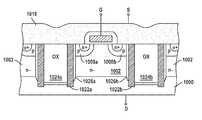
- FIGS. 10 a - 10 cshow cross sectional views of three power MOSFET cell arrays each of which includes strips of semi-insulating material (e.g., oxygen-doped polysilicon SiPOS) along the trench sidewalls.
- semi-insulating materiale.g., oxygen-doped polysilicon SiPOS
- wide insulation-filled trenches 1004 a,bare used to achieve improved thermal performance as in previous embodiments.
- the semi-insulating strips in these structuresfunction similar to polysilicon 106 a,b in the prior art FIG. 1 in pushing the depletion region deeper into the drift region, thus improving the breakdown voltage.
- strips 1006 a,b of semi-insulating materialextend along the trench sidewalls and are insulated from epitaxial region 1002 and body regions 1008 a,b by a layer of insulating material 1010 a,b .
- Strips 1006 a,bare in electrical contact with the top metal layer 1018 , and thus are biased to the same potential as the source and body regions.
- strips 1020 a,b of semi-insulating materialare integrated in the cell array in a similar manner to those in FIG. 10 a except that strips 1020 a,b are insulated from the top metal layer 1018 and thus are floating.
- the potential in the space charge regioncouples to the semi-insulating strips through insulation layers 1010 a,b to bias the strips to a corresponding mostly uniform potential.
- the insulation-filled trenches 1024 a,bextend all the way through epitaxial region 1002 and terminate in substrate 1000 .
- Semi-insulating strips 1022 a,bextend along the sidewalls of the trenches and electrically contact the source terminal through the top metal layer 1018 and the drain terminal through substrate region 1000 . Thus, the strips form a resistive connection between drain and source terminals. During operation, the strips acquire a linear voltage gradient with the highest potential (i.e., drain potential) at their bottom to lowest potential (i.e., source potential) at their top.
- Strips 1022 a,bare insulated from epitaxial regions 1002 by insulating layers 1026 a,b .
- the gate structure in FIG. 10 c as well as in FIGS. 10 a and 10 bis similar to the previous embodiments.
- the semi-insulating strips in the structures of FIGS. 10 a - 10 cserve as an additional tool by which the electrical characteristics of the device can be optimized. Depending on the application and the design targets, one structure may be preferred over the other.
- the resistivity of the strips of semi-insulating material in each of the FIGS. 10 a , 10 b , 10 c structurescan be adjusted and potentially varied from the top to the bottom to enable shaping of the space charge region formation in response to the applied drain-source voltage VDS.
- An exemplary set of process steps for forming the structure in FIG. 10 ais as follows.
- a hard maskis used to etch the silicon back to form wide trenches as in previous embodiments with wide trenches.
- a layer of thermally grown oxide having a thickness in the range of 200-1000 ⁇is then formed along the inner walls and bottom of the trench.
- About 4000 ⁇ of conformal oxideis then deposited over the thermally grown oxide layer.
- Oxygen-doped polysilicon (SiPOS)is then deposited in the trench regions and etched to form strips 1008 a,b along the sidewalls.
- the trenchesare then filled with insulation using conventional methods (e.g., SOG method), followed by planarization of the oxide surface.
- Conventional steps used in forming self-aligned gate DMOS structuresare then carried out to form the full cell structure as shown in FIG. 10 a.
- the depth of the trenches in the different embodiments described abovemay vary depending on the desired device performance and the target application for the device. For example, for high breakdown voltage (e.g., greater than 70V), the trenches may be extended deeper into the epitaxial region (e.g., to a depth of about 5 ⁇ m). As another example, the trenches can be extended all the way through the epitaxial region to meet the substrate regions (as in FIG. 10 c ). For lower voltage applications, the p regions (e.g., the floating p regions in FIG. 2 and the p strips in FIG. 8 ) need not extend deep into the epitaxial region since the device is not required to meet high breakdown voltages, and also to minimize the contribution of the p regions to the output capacitance.
- high breakdown voltagee.g., greater than 70V
- the trenchesmay be extended deeper into the epitaxial region (e.g., to a depth of about 5 ⁇ m).
- the trenchescan be extended all the way through the epi
- trench structures in the different embodiments described aboveare shown in combination with the gate structure of conventional DMOS cells, the invention is not limited as such.
- Two examples of other gate structures with which these trench structures may be combinedare shown in FIGS. 11 and 12 . These two cell structures have the benefit of lower gate to drain capacitance which in combination with the low output capacitance of the trench structures yields power devices particularly suitable for high frequency applications.
- FIG. 11 structureis similar to that in FIG. 8 except that a substantial portion of the gate extending over the surface of the drift region is eliminated. Thus, the gate to drain capacitance is reduced by an amount corresponding to the eliminated portion of the gate.
- the trench structure in FIG. 8is combined with the gate structure of a conventional UMOS cell.
- the advantages of the UMOS celle.g., low on-resistance
- the depth of p strips 1208 a,bis relatively shallow (e.g., in the range of 1.5 ⁇ m to 3 ⁇ m).
- the vertical charge control enabled by the resistive elements located along the insulation-filled trenchesallows the cells to be laterally spaced apart without impacting the electrical characteristics of the device. With the cells spaced further apart, the heat generated by each cell is distributed over a larger area and less heat interaction occurs between adjacent cells. A lower device temperature is thus achieved.
- each of the above cell structurescan be modified to become a quasi-vertically conducting structure by including a highly-doped n-type buried layer extending along the interface between the epitaxial region and the underlying highly-doped substrate region. At convenient locations, the buried layer is extended vertically to the top surface where it can be contacted to form the drain terminal of the device.
- the substrate regionmay be n-type or p-type depending on the application of the MOSFET.
- edge termination structures with breakdown voltages equal to or greater than that of the individual cellsare required to achieve a high device breakdown voltage.
- simulation resultsindicate that terminating at the outer edge of the device with a trench structure like trench 804 b would result in higher electric fields due to the electric field transition up to the top surface at the outside of the outer trench.
- An edge termination structure which yields the same or higher breakdown voltage than the cell structure in FIG. 8is shown in FIG. 13 .
- the active gate over the drift region between the outer two trenches 1306 b and 1306 cis eliminated allowing the drift region spacing Lt between these outer two trenches to be reduced to less than the drift region spacing Lc in the cell structures.
- the active gatehowever may be left in if obtaining the Lt spacing does not require its removal.
- the outer p strip 1308 dis not biased (i.e., is floating), and may be eliminated if desired.
- a conventional field plate structure 1310is optionally included in FIG. 13 .
- the gate structureis included between trenches 1306 b and 1306 c , with spacing Lt equaling spacing Lc.
- the p strip immediately to the right of the gate structure between trenches 1306 b and 1306 ci.e., the p strip corresponding to the strip along the left side of trench 1306 c
- the source and thus floatsis not connected to the source and thus floats.
- FIG. 13 embodimentfloating guard-rings may be used on the outside of trench 1306 c with or without field plate structure 1310 .
- cell trenches 1306 a,b and termination trench 1306 care shown to be narrower than the cell trenches in FIG. 8
- trenches 1306 a,b,cmay be widened as in FIG. 8 .
- the width Wt of termination trench 1306 cmay be designed to be different than cell that of trenches 1306 a,b if desired.
- FIG. 14is a cross sectional view showing another termination structure in combination with the cell structure shown in FIG. 8 .
- the termination structureincludes a termination trench 1408 lined with an insulation layer 1410 along its sidewalls and bottom.
- a field plate 1406(e.g., from doped polysilicon) is provided over insulation layer 1410 in trench 1408 , and extends laterally over the surface and away from the active regions.
- termination structuresare shown in combination with the cell structure in FIG. 8 , these and other known termination structures may be combined with any of the cell structures described above.
Landscapes
- Insulated Gate Type Field-Effect Transistor (AREA)
Abstract
Description
Claims (13)
Priority Applications (2)
| Application Number | Priority Date | Filing Date | Title |
|---|---|---|---|
| US11/862,396US7977744B2 (en) | 2002-07-18 | 2007-09-27 | Field effect transistor with trench filled with insulating material and strips of semi-insulating material along trench sidewalls |
| US13/114,253US20110284955A1 (en) | 2002-07-18 | 2011-05-24 | Field effect transistor with trench filled with insulating material and strips of semi-insulating material along trench sidewalls |
Applications Claiming Priority (3)
| Application Number | Priority Date | Filing Date | Title |
|---|---|---|---|
| US10/200,056US6803626B2 (en) | 2002-07-18 | 2002-07-18 | Vertical charge control semiconductor device |
| US10/931,887US7291894B2 (en) | 2002-07-18 | 2004-08-31 | Vertical charge control semiconductor device with low output capacitance |
| US11/862,396US7977744B2 (en) | 2002-07-18 | 2007-09-27 | Field effect transistor with trench filled with insulating material and strips of semi-insulating material along trench sidewalls |
Related Parent Applications (2)
| Application Number | Title | Priority Date | Filing Date |
|---|---|---|---|
| US10/200,056DivisionUS6803626B2 (en) | 2001-01-30 | 2002-07-18 | Vertical charge control semiconductor device |
| US10/931,887DivisionUS7291894B2 (en) | 2002-07-18 | 2004-08-31 | Vertical charge control semiconductor device with low output capacitance |
Related Child Applications (1)
| Application Number | Title | Priority Date | Filing Date |
|---|---|---|---|
| US13/114,253DivisionUS20110284955A1 (en) | 2002-07-18 | 2011-05-24 | Field effect transistor with trench filled with insulating material and strips of semi-insulating material along trench sidewalls |
Publications (2)
| Publication Number | Publication Date |
|---|---|
| US20080012071A1 US20080012071A1 (en) | 2008-01-17 |
| US7977744B2true US7977744B2 (en) | 2011-07-12 |
Family
ID=30443472
Family Applications (4)
| Application Number | Title | Priority Date | Filing Date |
|---|---|---|---|
| US10/200,056Expired - LifetimeUS6803626B2 (en) | 2001-01-30 | 2002-07-18 | Vertical charge control semiconductor device |
| US10/931,887Expired - LifetimeUS7291894B2 (en) | 2002-07-18 | 2004-08-31 | Vertical charge control semiconductor device with low output capacitance |
| US11/862,396Expired - Fee RelatedUS7977744B2 (en) | 2002-07-18 | 2007-09-27 | Field effect transistor with trench filled with insulating material and strips of semi-insulating material along trench sidewalls |
| US13/114,253AbandonedUS20110284955A1 (en) | 2002-07-18 | 2011-05-24 | Field effect transistor with trench filled with insulating material and strips of semi-insulating material along trench sidewalls |
Family Applications Before (2)
| Application Number | Title | Priority Date | Filing Date |
|---|---|---|---|
| US10/200,056Expired - LifetimeUS6803626B2 (en) | 2001-01-30 | 2002-07-18 | Vertical charge control semiconductor device |
| US10/931,887Expired - LifetimeUS7291894B2 (en) | 2002-07-18 | 2004-08-31 | Vertical charge control semiconductor device with low output capacitance |
Family Applications After (1)
| Application Number | Title | Priority Date | Filing Date |
|---|---|---|---|
| US13/114,253AbandonedUS20110284955A1 (en) | 2002-07-18 | 2011-05-24 | Field effect transistor with trench filled with insulating material and strips of semi-insulating material along trench sidewalls |
Country Status (1)
| Country | Link |
|---|---|
| US (4) | US6803626B2 (en) |
Cited By (3)
| Publication number | Priority date | Publication date | Assignee | Title |
|---|---|---|---|---|
| US20110284955A1 (en)* | 2002-07-18 | 2011-11-24 | Fairchild Semiconductor Corporation | Field effect transistor with trench filled with insulating material and strips of semi-insulating material along trench sidewalls |
| US20120306009A1 (en)* | 2011-06-03 | 2012-12-06 | Suku Kim | Integration of superjunction mosfet and diode |
| CN103378173A (en)* | 2012-04-29 | 2013-10-30 | 朱江 | Schottky semiconductor device with charge compensation and manufacturing method thereof |
Families Citing this family (73)
| Publication number | Priority date | Publication date | Assignee | Title |
|---|---|---|---|---|
| US7652326B2 (en) | 2003-05-20 | 2010-01-26 | Fairchild Semiconductor Corporation | Power semiconductor devices and methods of manufacture |
| JP4209260B2 (en)* | 2003-06-04 | 2009-01-14 | Necエレクトロニクス株式会社 | Semiconductor device and manufacturing method thereof |
| KR100702786B1 (en)* | 2004-02-06 | 2007-04-03 | 매그나칩 반도체 유한회사 | Electrostatic discharge protection element and its circuit |
| JP2006040982A (en)* | 2004-07-22 | 2006-02-09 | Fairchild Semiconductor Corp | Vertical charge control semiconductor device with low output capacity |
| US20060043479A1 (en)* | 2004-09-02 | 2006-03-02 | Patrice Parris | Metal oxide semiconductor device including a shielding structure for low gate-drain capacitance |
| JP4734968B2 (en)* | 2005-03-04 | 2011-07-27 | トヨタ自動車株式会社 | Insulated gate semiconductor device |
| US20060255401A1 (en)* | 2005-05-11 | 2006-11-16 | Yang Robert K | Increasing breakdown voltage in semiconductor devices with vertical series capacitive structures |
| KR101296984B1 (en)* | 2005-06-10 | 2013-08-14 | 페어차일드 세미컨덕터 코포레이션 | Charge balance field effect transistor |
| TWI400757B (en)* | 2005-06-29 | 2013-07-01 | Fairchild Semiconductor | Method for forming a shadow gate field effect transistor |
| JP2007027193A (en)* | 2005-07-12 | 2007-02-01 | Renesas Technology Corp | Semiconductor device, method for manufacturing the same, and non-insulated DC / DC converter |
| US20070012983A1 (en)* | 2005-07-15 | 2007-01-18 | Yang Robert K | Terminations for semiconductor devices with floating vertical series capacitive structures |
| US7514743B2 (en)* | 2005-08-23 | 2009-04-07 | Robert Kuo-Chang Yang | DMOS transistor with floating poly-filled trench for improved performance through 3-D field shaping |
| WO2008012737A2 (en)* | 2006-07-24 | 2008-01-31 | Nxp B.V. | Method of manufacturing a semiconductor device and a device manufactured by the method |
| JP2008140824A (en)* | 2006-11-30 | 2008-06-19 | Toshiba Corp | Semiconductor device |
| TWI357108B (en)* | 2007-08-21 | 2012-01-21 | Nat Univ Tsing Hua | Semiconductor device structure |
| US7880224B2 (en)* | 2008-01-25 | 2011-02-01 | Infineon Technologies Austria Ag | Semiconductor component having discontinuous drift zone control dielectric arranged between drift zone and drift control zone and a method of making the same |
| US7807576B2 (en)* | 2008-06-20 | 2010-10-05 | Fairchild Semiconductor Corporation | Structure and method for forming a thick bottom dielectric (TBD) for trench-gate devices |
| US20120273916A1 (en) | 2011-04-27 | 2012-11-01 | Yedinak Joseph A | Superjunction Structures for Power Devices and Methods of Manufacture |
| US8378416B2 (en)* | 2008-12-01 | 2013-02-19 | Maxpower Semiconductor, Inc. | MOS-gated power devices, methods, and integrated circuits |
| US8174067B2 (en) | 2008-12-08 | 2012-05-08 | Fairchild Semiconductor Corporation | Trench-based power semiconductor devices with increased breakdown voltage characteristics |
| US8304829B2 (en) | 2008-12-08 | 2012-11-06 | Fairchild Semiconductor Corporation | Trench-based power semiconductor devices with increased breakdown voltage characteristics |
| US8227855B2 (en) | 2009-02-09 | 2012-07-24 | Fairchild Semiconductor Corporation | Semiconductor devices with stable and controlled avalanche characteristics and methods of fabricating the same |
| US8148749B2 (en) | 2009-02-19 | 2012-04-03 | Fairchild Semiconductor Corporation | Trench-shielded semiconductor device |
| US8049276B2 (en) | 2009-06-12 | 2011-11-01 | Fairchild Semiconductor Corporation | Reduced process sensitivity of electrode-semiconductor rectifiers |
| WO2011008717A2 (en)* | 2009-07-13 | 2011-01-20 | Maxpower Semiconductor Inc. | Integrated power supplies and combined high-side plus low-side switches |
| US20110049638A1 (en)* | 2009-09-01 | 2011-03-03 | Stmicroelectronics S.R.L. | Structure for high voltage device and corresponding integration process |
| US8129778B2 (en)* | 2009-12-02 | 2012-03-06 | Fairchild Semiconductor Corporation | Semiconductor devices and methods for making the same |
| US20110198689A1 (en)* | 2010-02-17 | 2011-08-18 | Suku Kim | Semiconductor devices containing trench mosfets with superjunctions |
| US8598654B2 (en) | 2011-03-16 | 2013-12-03 | Fairchild Semiconductor Corporation | MOSFET device with thick trench bottom oxide |
| US8786010B2 (en) | 2011-04-27 | 2014-07-22 | Fairchild Semiconductor Corporation | Superjunction structures for power devices and methods of manufacture |
| US8772868B2 (en) | 2011-04-27 | 2014-07-08 | Fairchild Semiconductor Corporation | Superjunction structures for power devices and methods of manufacture |
| US8836028B2 (en) | 2011-04-27 | 2014-09-16 | Fairchild Semiconductor Corporation | Superjunction structures for power devices and methods of manufacture |
| US8673700B2 (en)* | 2011-04-27 | 2014-03-18 | Fairchild Semiconductor Corporation | Superjunction structures for power devices and methods of manufacture |
| US9224852B2 (en) | 2011-08-25 | 2015-12-29 | Alpha And Omega Semiconductor Incorporated | Corner layout for high voltage semiconductor devices |
| US8680613B2 (en) | 2012-07-30 | 2014-03-25 | Alpha And Omega Semiconductor Incorporated | Termination design for high voltage device |
| US8785279B2 (en) | 2012-07-30 | 2014-07-22 | Alpha And Omega Semiconductor Incorporated | High voltage field balance metal oxide field effect transistor (FBM) |
| TWI587503B (en)* | 2012-01-11 | 2017-06-11 | 世界先進積體電路股份有限公司 | Semiconductor device and method of manufacturing same |
| US9685511B2 (en) | 2012-05-21 | 2017-06-20 | Infineon Technologies Austria Ag | Semiconductor device and method for manufacturing a semiconductor device |
| US20130320512A1 (en) | 2012-06-05 | 2013-12-05 | Infineon Technologies Austria Ag | Semiconductor Device and Method of Manufacturing a Semiconductor Device |
| US9048115B2 (en)* | 2012-10-26 | 2015-06-02 | Vanguard International Semiconductor Corporation | Superjunction transistor with implantation barrier at the bottom of a trench |
| TWI473267B (en) | 2012-11-06 | 2015-02-11 | Ind Tech Res Inst | Gold oxygen half field effect transistor |
| TWI506705B (en)* | 2012-11-14 | 2015-11-01 | Vanguard Int Semiconduct Corp | Semiconductor device and methods for forming the same |
| US8809948B1 (en) | 2012-12-21 | 2014-08-19 | Alpha And Omega Semiconductor Incorporated | Device structure and methods of making high density MOSFETs for load switch and DC-DC applications |
| US8753935B1 (en) | 2012-12-21 | 2014-06-17 | Alpha And Omega Semiconductor Incorporated | High frequency switching MOSFETs with low output capacitance using a depletable P-shield |
| US8951867B2 (en) | 2012-12-21 | 2015-02-10 | Alpha And Omega Semiconductor Incorporated | High density trench-based power MOSFETs with self-aligned active contacts and method for making such devices |
| US9105494B2 (en)* | 2013-02-25 | 2015-08-11 | Alpha and Omega Semiconductors, Incorporated | Termination trench for power MOSFET applications |
| US10249721B2 (en) | 2013-04-04 | 2019-04-02 | Infineon Technologies Austria Ag | Semiconductor device including a gate trench and a source trench |
| TWI542006B (en)* | 2013-06-21 | 2016-07-11 | 竹懋科技股份有限公司 | Ditch type MOS rectifying element and manufacturing method thereof |
| JP2015023251A (en)* | 2013-07-23 | 2015-02-02 | ソニー株式会社 | Multilayer wiring board and manufacturing method therefor, and semiconductor product |
| KR101514537B1 (en)* | 2013-08-09 | 2015-04-22 | 삼성전기주식회사 | Power semiconductor device and method of fabricating the same |
| US9666663B2 (en) | 2013-08-09 | 2017-05-30 | Infineon Technologies Ag | Semiconductor device with cell trench structures and contacts and method of manufacturing a semiconductor device |
| CN104425598A (en)* | 2013-08-27 | 2015-03-18 | 上海华虹宏力半导体制造有限公司 | Asymmetric plane-gate super-junction metal-oxide-semiconductor field effect transistor and manufacturing method thereof |
| US9076838B2 (en)* | 2013-09-13 | 2015-07-07 | Infineon Technologies Ag | Insulated gate bipolar transistor with mesa sections between cell trench structures and method of manufacturing |
| CN104518021A (en)* | 2013-09-26 | 2015-04-15 | 无锡华润华晶微电子有限公司 | VDMOS device cellular structure and manufacture method thereof |
| US9105679B2 (en) | 2013-11-27 | 2015-08-11 | Infineon Technologies Ag | Semiconductor device and insulated gate bipolar transistor with barrier regions |
| US9385228B2 (en) | 2013-11-27 | 2016-07-05 | Infineon Technologies Ag | Semiconductor device with cell trench structures and contacts and method of manufacturing a semiconductor device |
| US9985094B2 (en)* | 2013-12-27 | 2018-05-29 | Taiwan Semiconductor Manufacturing Company, Ltd. | Super junction with an angled trench, transistor having the super junction and method of making the same |
| US9484404B2 (en) | 2014-01-29 | 2016-11-01 | Stmicroelectronics S.R.L. | Electronic device of vertical MOS type with termination trenches having variable depth |
| US9553179B2 (en) | 2014-01-31 | 2017-01-24 | Infineon Technologies Ag | Semiconductor device and insulated gate bipolar transistor with barrier structure |
| US9564515B2 (en)* | 2014-07-28 | 2017-02-07 | Taiwan Semiconductor Manufacturing Co., Ltd. | Semiconductor device having super junction structure and method for manufacturing the same |
| CN105529369B (en)* | 2016-03-08 | 2019-05-14 | 中国电子科技集团公司第二十四研究所 | A kind of semiconductor structure cell and power semiconductor |
| CN106847700B (en)* | 2017-03-07 | 2022-03-15 | 中山汉臣电子科技有限公司 | High-voltage VDMOS structure and preparation method thereof |
| CN108666313B (en)* | 2017-03-30 | 2021-01-12 | 联华电子股份有限公司 | Semiconductor structure for improving dynamic random access memory row hammer phenomenon and manufacturing method thereof |
| CN110164957B (en)* | 2017-04-18 | 2022-04-26 | 中国电子科技集团公司第二十四研究所 | High Voltage Semiconductor Dielectric Withstand Voltage Terminal |
| CN107221561A (en)* | 2017-06-29 | 2017-09-29 | 全球能源互联网研究院 | A kind of lamination Electric Field Modulated high-voltage MOSFET structure and preparation method thereof |
| JP7143575B2 (en)* | 2017-07-18 | 2022-09-29 | 富士電機株式会社 | semiconductor equipment |
| EP3474331A1 (en)* | 2017-10-19 | 2019-04-24 | Infineon Technologies Austria AG | Semiconductor device and method for fabricating a semiconductor device |
| JP6818712B2 (en)* | 2018-03-22 | 2021-01-20 | 株式会社東芝 | Semiconductor device |
| CN108766884A (en)* | 2018-08-03 | 2018-11-06 | 淄博汉林半导体有限公司 | Schottky chip manufacturing method and Schottky chip without lithography step |
| CN113270495A (en)* | 2020-02-14 | 2021-08-17 | 苏州华太电子技术有限公司 | VDMOSFET device structure and manufacturing method thereof |
| CN113270471A (en)* | 2020-02-14 | 2021-08-17 | 苏州华太电子技术有限公司 | Terminal structure of VDMOSFET device and manufacturing method thereof |
| CN114188395A (en)* | 2021-10-09 | 2022-03-15 | 无锡先瞳半导体科技有限公司 | Charge compensation type shielded gate trench power device and preparation method thereof |
| CN114566548A (en)* | 2022-01-27 | 2022-05-31 | 无锡先瞳半导体科技有限公司 | Groove type field effect transistor with longitudinal P type source region and preparation method thereof |
Citations (262)
| Publication number | Priority date | Publication date | Assignee | Title |
|---|---|---|---|---|
| US3404295A (en) | 1964-11-30 | 1968-10-01 | Motorola Inc | High frequency and voltage transistor with added region for punch-through protection |
| US3412297A (en) | 1965-12-16 | 1968-11-19 | United Aircraft Corp | Mos field-effect transistor with a onemicron vertical channel |
| US3497777A (en) | 1967-06-13 | 1970-02-24 | Stanislas Teszner | Multichannel field-effect semi-conductor device |
| US3564356A (en) | 1968-10-24 | 1971-02-16 | Tektronix Inc | High voltage integrated circuit transistor |
| US3660697A (en) | 1970-02-16 | 1972-05-02 | Bell Telephone Labor Inc | Monolithic semiconductor apparatus adapted for sequential charge transfer |
| US4003072A (en) | 1972-04-20 | 1977-01-11 | Sony Corporation | Semiconductor device with high voltage breakdown resistance |
| US4300150A (en) | 1980-06-16 | 1981-11-10 | North American Philips Corporation | Lateral double-diffused MOS transistor device |
| US4326332A (en) | 1980-07-28 | 1982-04-27 | International Business Machines Corp. | Method of making a high density V-MOS memory array |
| US4337474A (en) | 1978-08-31 | 1982-06-29 | Mitsubishi Denki Kabushiki Kaisha | Semiconductor device |
| US4345265A (en) | 1980-04-14 | 1982-08-17 | Supertex, Inc. | MOS Power transistor with improved high-voltage capability |
| US4445202A (en) | 1980-11-12 | 1984-04-24 | International Business Machines Corporation | Electrically switchable permanent storage |
| US4579621A (en) | 1983-07-08 | 1986-04-01 | Mitsubishi Denki Kabushiki Kaisha | Selective epitaxial growth method |
| US4636281A (en) | 1984-06-14 | 1987-01-13 | Commissariat A L'energie Atomique | Process for the autopositioning of a local field oxide with respect to an insulating trench |
| US4638344A (en) | 1979-10-09 | 1987-01-20 | Cardwell Jr Walter T | Junction field-effect transistor controlled by merged depletion regions |
| US4639761A (en) | 1983-12-16 | 1987-01-27 | North American Philips Corporation | Combined bipolar-field effect transistor resurf devices |
| US4698653A (en) | 1979-10-09 | 1987-10-06 | Cardwell Jr Walter T | Semiconductor devices controlled by depletion regions |
| US4716126A (en) | 1986-06-05 | 1987-12-29 | Siliconix Incorporated | Fabrication of double diffused metal oxide semiconductor transistor |
| US4746630A (en) | 1986-09-17 | 1988-05-24 | Hewlett-Packard Company | Method for producing recessed field oxide with improved sidewall characteristics |
| US4754310A (en) | 1980-12-10 | 1988-06-28 | U.S. Philips Corp. | High voltage semiconductor device |
| US4774556A (en) | 1985-07-25 | 1988-09-27 | Nippondenso Co., Ltd. | Non-volatile semiconductor memory device |
| US4801986A (en) | 1987-04-03 | 1989-01-31 | General Electric Company | Vertical double diffused metal oxide semiconductor VDMOS device with increased safe operating area and method |
| US4821095A (en) | 1987-03-12 | 1989-04-11 | General Electric Company | Insulated gate semiconductor device with extra short grid and method of fabrication |
| US4823176A (en) | 1987-04-03 | 1989-04-18 | General Electric Company | Vertical double diffused metal oxide semiconductor (VDMOS) device including high voltage junction exhibiting increased safe operating area |
| US4853345A (en) | 1988-08-22 | 1989-08-01 | Delco Electronics Corporation | Process for manufacture of a vertical DMOS transistor |
| US4868624A (en) | 1980-05-09 | 1989-09-19 | Regents Of The University Of Minnesota | Channel collector transistor |
| US4893160A (en) | 1987-11-13 | 1990-01-09 | Siliconix Incorporated | Method for increasing the performance of trenched devices and the resulting structure |
| US4914058A (en) | 1987-12-29 | 1990-04-03 | Siliconix Incorporated | Grooved DMOS process with varying gate dielectric thickness |
| US4941026A (en) | 1986-12-05 | 1990-07-10 | General Electric Company | Semiconductor devices exhibiting minimum on-resistance |
| US4967245A (en) | 1988-03-14 | 1990-10-30 | Siliconix Incorporated | Trench power MOSFET device |
| US4974059A (en) | 1982-12-21 | 1990-11-27 | International Rectifier Corporation | Semiconductor high-power mosfet device |
| US4990463A (en) | 1988-07-05 | 1991-02-05 | Kabushiki Kaisha Toshiba | Method of manufacturing capacitor |
| US4992390A (en) | 1989-07-06 | 1991-02-12 | General Electric Company | Trench gate structure with thick bottom oxide |
| US5027180A (en) | 1986-12-11 | 1991-06-25 | Mitsubishi Electric Corporation | Double gate static induction thyristor |
| US5034785A (en) | 1986-03-24 | 1991-07-23 | Siliconix Incorporated | Planar vertical channel DMOS structure |
| US5072266A (en) | 1988-12-27 | 1991-12-10 | Siliconix Incorporated | Trench DMOS power transistor with field-shaping body profile and three-dimensional geometry |
| US5071782A (en) | 1990-06-28 | 1991-12-10 | Texas Instruments Incorporated | Vertical memory cell array and method of fabrication |
| US5079608A (en) | 1990-11-06 | 1992-01-07 | Harris Corporation | Power MOSFET transistor circuit with active clamp |
| US5105243A (en) | 1987-02-26 | 1992-04-14 | Kabushiki Kaisha Toshiba | Conductivity-modulation metal oxide field effect transistor with single gate structure |
| US5111253A (en) | 1989-05-09 | 1992-05-05 | General Electric Company | Multicellular FET having a Schottky diode merged therewith |
| US5142640A (en) | 1988-06-02 | 1992-08-25 | Seiko Epson Corporation | Trench gate metal oxide semiconductor field effect transistor |
| US5164802A (en) | 1991-03-20 | 1992-11-17 | Harris Corporation | Power vdmosfet with schottky on lightly doped drain of lateral driver fet |
| US5164325A (en) | 1987-10-08 | 1992-11-17 | Siliconix Incorporated | Method of making a vertical current flow field effect transistor |
| US5216275A (en) | 1991-03-19 | 1993-06-01 | University Of Electronic Science And Technology Of China | Semiconductor power devices with alternating conductivity type high-voltage breakdown regions |
| US5219793A (en) | 1991-06-03 | 1993-06-15 | Motorola Inc. | Method for forming pitch independent contacts and a semiconductor device having the same |
| US5219777A (en) | 1991-06-14 | 1993-06-15 | Gold Star Electron Co., Ltd. | Metal oxide semiconductor field effect transistor and method of making the same |
| US5233215A (en) | 1992-06-08 | 1993-08-03 | North Carolina State University At Raleigh | Silicon carbide power MOSFET with floating field ring and floating field plate |
| US5262336A (en) | 1986-03-21 | 1993-11-16 | Advanced Power Technology, Inc. | IGBT process to produce platinum lifetime control |
| US5268311A (en) | 1988-09-01 | 1993-12-07 | International Business Machines Corporation | Method for forming a thin dielectric layer on a substrate |
| DE4300806C1 (en) | 1993-01-14 | 1993-12-23 | Siemens Ag | Vertical MOS transistor prodn. - with reduced trench spacing, without parasitic bipolar effects |
| US5275965A (en) | 1992-11-25 | 1994-01-04 | Micron Semiconductor, Inc. | Trench isolation using gated sidewalls |
| US5294824A (en) | 1992-07-31 | 1994-03-15 | Motorola, Inc. | High voltage transistor having reduced on-resistance |
| US5298761A (en) | 1991-06-17 | 1994-03-29 | Nikon Corporation | Method and apparatus for exposure process |
| US5300447A (en) | 1992-09-29 | 1994-04-05 | Texas Instruments Incorporated | Method of manufacturing a minimum scaled transistor |
| US5326711A (en) | 1993-01-04 | 1994-07-05 | Texas Instruments Incorporated | High performance high voltage vertical transistor and method of fabrication |
| US5350937A (en) | 1991-10-08 | 1994-09-27 | Semiconductor Energy Laboratory Co., Ltd. | Non-volatile memory device having a floating gate |
| US5365102A (en) | 1993-07-06 | 1994-11-15 | North Carolina State University | Schottky barrier rectifier with MOS trench |
| US5366914A (en) | 1992-01-29 | 1994-11-22 | Nec Corporation | Vertical power MOSFET structure having reduced cell area |
| US5389815A (en) | 1992-04-28 | 1995-02-14 | Mitsubishi Denki Kabushiki Kaisha | Semiconductor diode with reduced recovery current |
| US5405794A (en) | 1994-06-14 | 1995-04-11 | Philips Electronics North America Corporation | Method of producing VDMOS device of increased power density |
| US5418376A (en) | 1993-03-02 | 1995-05-23 | Toyo Denki Seizo Kabushiki Kaisha | Static induction semiconductor device with a distributed main electrode structure and static induction semiconductor device with a static induction main electrode shorted structure |
| US5424231A (en) | 1994-08-09 | 1995-06-13 | United Microelectronics Corp. | Method for manufacturing a VDMOS transistor |
| US5429977A (en) | 1994-03-11 | 1995-07-04 | Industrial Technology Research Institute | Method for forming a vertical transistor with a stacked capacitor DRAM cell |
| US5430324A (en) | 1992-07-23 | 1995-07-04 | Siliconix, Incorporated | High voltage transistor having edge termination utilizing trench technology |
| US5430311A (en) | 1991-09-20 | 1995-07-04 | Hitachi, Ltd. | Constant-voltage diode for over-voltage protection |
| US5434435A (en) | 1994-05-04 | 1995-07-18 | North Carolina State University | Trench gate lateral MOSFET |
| US5436189A (en) | 1989-10-03 | 1995-07-25 | Harris Corporation | Self-aligned channel stop for trench-isolated island |
| US5438215A (en) | 1993-03-25 | 1995-08-01 | Siemens Aktiengesellschaft | Power MOSFET |
| US5473176A (en) | 1993-09-01 | 1995-12-05 | Kabushiki Kaisha Toshiba | Vertical insulated gate transistor and method of manufacture |
| US5473180A (en) | 1993-07-12 | 1995-12-05 | U.S. Philips Corporation | Semiconductor device with an MOST provided with an extended drain region for high voltages |
| US5474943A (en) | 1993-03-15 | 1995-12-12 | Siliconix Incorporated | Method for fabricating a short channel trenched DMOS transistor |
| US5519245A (en) | 1989-08-31 | 1996-05-21 | Nippondenso Co., Ltd. | Insulated gate bipolar transistor with reverse conducting current |
| US5539238A (en) | 1992-09-02 | 1996-07-23 | Texas Instruments Incorporated | Area efficient high voltage Mosfets with vertical resurf drift regions |
| US5541425A (en) | 1994-01-20 | 1996-07-30 | Mitsubishi Denki Kabushiki Kaisha | Semiconductor device having trench structure |
| US5554862A (en) | 1992-03-31 | 1996-09-10 | Kabushiki Kaisha Toshiba | Power semiconductor device |
| US5567634A (en) | 1995-05-01 | 1996-10-22 | National Semiconductor Corporation | Method of fabricating self-aligned contact trench DMOS transistors |
| US5567635A (en) | 1992-03-23 | 1996-10-22 | International Business Machines Corporation | Method of making a three dimensional trench EEPROM cell structure |
| US5572048A (en) | 1992-11-20 | 1996-11-05 | Hitachi, Ltd. | Voltage-driven type semiconductor device |
| US5578851A (en) | 1994-08-15 | 1996-11-26 | Siliconix Incorporated | Trenched DMOS transistor having thick field oxide in termination region |
| US5581100A (en) | 1994-08-30 | 1996-12-03 | International Rectifier Corporation | Trench depletion MOSFET |
| US5583065A (en) | 1994-11-23 | 1996-12-10 | Sony Corporation | Method of making a MOS semiconductor device |
| US5592005A (en) | 1995-03-31 | 1997-01-07 | Siliconix Incorporated | Punch-through field effect transistor |
| US5595927A (en) | 1995-03-17 | 1997-01-21 | Taiwan Semiconductor Manufacturing Company Ltd. | Method for making self-aligned source/drain mask ROM memory cell using trench etched channel |
| US5597765A (en) | 1995-01-10 | 1997-01-28 | Siliconix Incorporated | Method for making termination structure for power MOSFET |
| US5616945A (en) | 1995-10-13 | 1997-04-01 | Siliconix Incorporated | Multiple gated MOSFET for use in DC-DC converter |
| US5623152A (en) | 1995-02-09 | 1997-04-22 | Mitsubishi Denki Kabushiki Kaisha | Insulated gate semiconductor device |
| US5629543A (en) | 1995-08-21 | 1997-05-13 | Siliconix Incorporated | Trenched DMOS transistor with buried layer for reduced on-resistance and ruggedness |
| US5635419A (en) | 1994-10-28 | 1997-06-03 | International Business Machines Corporation | Porous silicon trench and capacitor structures |
| US5637898A (en) | 1995-12-22 | 1997-06-10 | North Carolina State University | Vertical field effect transistors having improved breakdown voltage capability and low on-state resistance |
| US5640034A (en) | 1992-05-18 | 1997-06-17 | Texas Instruments Incorporated | Top-drain trench based resurf DMOS transistor structure |
| US5648670A (en) | 1995-06-07 | 1997-07-15 | Sgs-Thomson Microelectronics, Inc. | Trench MOS-gated device with a minimum number of masks |
| US5656843A (en) | 1992-08-05 | 1997-08-12 | U.S. Philips Corporation | Semiconductor device having a vertical insulated gate field effect device and a breakdown region remote from the gate |
| US5670803A (en) | 1995-02-08 | 1997-09-23 | International Business Machines Corporation | Three-dimensional SRAM trench structure and fabrication method therefor |
| US5689128A (en) | 1995-08-21 | 1997-11-18 | Siliconix Incorporated | High density trenched DMOS transistor |
| US5693569A (en) | 1995-01-26 | 1997-12-02 | Fuji Electric Co., Ltd. | Method of forming silicon carbide trench mosfet with a schottky electrode |
| CN1036666C (en) | 1987-01-09 | 1997-12-10 | 株式会社日立制作所 | heat-resistant steel |
| US5705409A (en) | 1995-09-28 | 1998-01-06 | Motorola Inc. | Method for forming trench transistor structure |
| US5710072A (en) | 1994-05-17 | 1998-01-20 | Siemens Aktiengesellschaft | Method of producing and arrangement containing self-amplifying dynamic MOS transistor memory cells |
| US5714781A (en) | 1995-04-27 | 1998-02-03 | Nippondenso Co., Ltd. | Semiconductor device having a gate electrode in a grove and a diffused region under the grove |
| US5719409A (en) | 1996-06-06 | 1998-02-17 | Cree Research, Inc. | Silicon carbide metal-insulator semiconductor field effect transistor |
| US5770878A (en) | 1996-04-10 | 1998-06-23 | Harris Corporation | Trench MOS gate device |
| US5776813A (en) | 1997-10-06 | 1998-07-07 | Industrial Technology Research Institute | Process to manufacture a vertical gate-enhanced bipolar transistor |
| US5780343A (en) | 1995-12-20 | 1998-07-14 | National Semiconductor Corporation | Method of producing high quality silicon surface for selective epitaxial growth of silicon |
| US5801417A (en) | 1988-05-17 | 1998-09-01 | Advanced Power Technology, Inc. | Self-aligned power MOSFET device with recessed gate and source |
| US5877528A (en) | 1997-03-03 | 1999-03-02 | Megamos Corporation | Structure to provide effective channel-stop in termination areas for trenched power transistors |
| US5879994A (en) | 1997-04-15 | 1999-03-09 | National Semiconductor Corporation | Self-aligned method of fabricating terrace gate DMOS transistor |
| US5879971A (en) | 1995-09-28 | 1999-03-09 | Motorola Inc. | Trench random access memory cell and method of formation |
| US5895951A (en) | 1996-04-05 | 1999-04-20 | Megamos Corporation | MOSFET structure and fabrication process implemented by forming deep and narrow doping regions through doping trenches |
| US5895952A (en) | 1994-12-30 | 1999-04-20 | Siliconix Incorporated | Trench MOSFET with multi-resistivity drain to provide low on-resistance |
| US5897360A (en) | 1996-10-21 | 1999-04-27 | Nec Corporation | Manufacturing method of semiconductor integrated circuit |
| US5897343A (en) | 1998-03-30 | 1999-04-27 | Motorola, Inc. | Method of making a power switching trench MOSFET having aligned source regions |
| US5900663A (en) | 1998-02-07 | 1999-05-04 | Xemod, Inc. | Quasi-mesh gate structure for lateral RF MOS devices |
| US5906680A (en) | 1986-09-12 | 1999-05-25 | International Business Machines Corporation | Method and apparatus for low temperature, low pressure chemical vapor deposition of epitaxial silicon layers |
| US5917216A (en) | 1995-02-10 | 1999-06-29 | Siliconix Incorporated | Trenched field effect transistor with PN depletion barrier |
| US5929481A (en) | 1996-07-19 | 1999-07-27 | Siliconix Incorporated | High density trench DMOS transistor with trench bottom implant |
| US5943581A (en) | 1997-11-05 | 1999-08-24 | Vanguard International Semiconductor Corporation | Method of fabricating a buried reservoir capacitor structure for high-density dynamic random access memory (DRAM) circuits |
| DE19736981C2 (en) | 1997-02-10 | 1999-08-26 | Mitsubishi Electric Corp | High breakdown voltage semiconductor device |
| US5949104A (en) | 1998-02-07 | 1999-09-07 | Xemod, Inc. | Source connection structure for lateral RF MOS devices |
| US5949124A (en) | 1995-10-31 | 1999-09-07 | Motorola, Inc. | Edge termination structure |
| US5960271A (en) | 1996-09-18 | 1999-09-28 | Advanced Micro Devices, Inc. | Short channel self-aligned VMOS field effect transistor |
| US5959324A (en) | 1992-03-30 | 1999-09-28 | Kabushiki Kaisha Toshiba | Semiconductor device including an improved terminal structure |
| US5972741A (en) | 1996-10-31 | 1999-10-26 | Sanyo Electric Co., Ltd. | Method of manufacturing semiconductor device |
| US5973367A (en) | 1995-10-13 | 1999-10-26 | Siliconix Incorporated | Multiple gated MOSFET for use in DC-DC converter |
| US5973360A (en) | 1996-03-20 | 1999-10-26 | Siemens Aktiengesellschaft | Field effect-controllable semiconductor component |
| US5976936A (en) | 1995-09-06 | 1999-11-02 | Denso Corporation | Silicon carbide semiconductor device |
| US5981996A (en) | 1995-02-17 | 1999-11-09 | Fuji Electric Co., Ltd. | Vertical trench misfet and method of manufacturing the same |
| US5981344A (en) | 1992-07-24 | 1999-11-09 | Siliconix Incorporated | Trench field effect transistor with reduced punch-through susceptibility and low RDSon |
| US5998833A (en) | 1998-10-26 | 1999-12-07 | North Carolina State University | Power semiconductor devices having improved high frequency switching and breakdown characteristics |
| US6005271A (en) | 1997-11-05 | 1999-12-21 | Magepower Semiconductor Corp. | Semiconductor cell array with high packing density |
| US6008097A (en) | 1996-12-14 | 1999-12-28 | Electronics And Telecommunications Research Institute | MOS transistor of semiconductor device and method of manufacturing the same |
| US6011298A (en) | 1996-12-31 | 2000-01-04 | Stmicroelectronics, Inc. | High voltage termination with buried field-shaping region |
| US6015727A (en) | 1998-06-08 | 2000-01-18 | Wanlass; Frank M. | Damascene formation of borderless contact MOS transistors |
| US6020250A (en) | 1994-08-11 | 2000-02-01 | International Business Machines Corporation | Stacked devices |
| JP2000040872A (en) | 1998-07-24 | 2000-02-08 | Senju Metal Ind Co Ltd | Method of soldering printed board, and jet solder vessel |
| US6037632A (en) | 1995-11-06 | 2000-03-14 | Kabushiki Kaisha Toshiba | Semiconductor device |
| US6037628A (en) | 1997-06-30 | 2000-03-14 | Intersil Corporation | Semiconductor structures with trench contacts |
| US6049108A (en) | 1995-06-02 | 2000-04-11 | Siliconix Incorporated | Trench-gated MOSFET with bidirectional voltage clamping |
| US6048772A (en) | 1998-05-04 | 2000-04-11 | Xemod, Inc. | Method for fabricating a lateral RF MOS device with an non-diffusion source-backside connection |
| US6057558A (en) | 1997-03-05 | 2000-05-02 | Denson Corporation | Silicon carbide semiconductor device and manufacturing method thereof |
| US6064088A (en) | 1998-06-15 | 2000-05-16 | Xemod, Inc. | RF power MOSFET device with extended linear region of transconductance characteristic at low drain current |
| US6063678A (en) | 1998-05-04 | 2000-05-16 | Xemod, Inc. | Fabrication of lateral RF MOS devices with enhanced RF properties |
| US6066878A (en) | 1997-11-10 | 2000-05-23 | Intersil Corporation | High voltage semiconductor structure |
| JP2000156978A (en) | 1998-11-17 | 2000-06-06 | Fuji Electric Co Ltd | Soft switching circuit |
| US6084264A (en) | 1998-11-25 | 2000-07-04 | Siliconix Incorporated | Trench MOSFET having improved breakdown and on-resistance characteristics |
| US6084268A (en) | 1996-03-05 | 2000-07-04 | Semiconductor Components Industries, Llc | Power MOSFET device having low on-resistance and method |
| US6087232A (en) | 1997-10-28 | 2000-07-11 | Electronics And Telecommunications Research Institute | Fabrication method of lateral double diffused MOS transistors |
| US6097063A (en) | 1996-01-22 | 2000-08-01 | Fuji Electric Co., Ltd. | Semiconductor device having a plurality of parallel drift regions |
| US6096608A (en) | 1997-06-30 | 2000-08-01 | Siliconix Incorporated | Bidirectional trench gated power mosfet with submerged body bus extending underneath gate trench |
| US6104054A (en) | 1998-05-13 | 2000-08-15 | Texas Instruments Incorporated | Space-efficient layout method to reduce the effect of substrate capacitance in dielectrically isolated process technologies |
| US6110799A (en) | 1997-06-30 | 2000-08-29 | Intersil Corporation | Trench contact process |
| US6114727A (en) | 1997-01-09 | 2000-09-05 | Kabushiki Kaisha Toshiba | Semiconductor device |
| JP2000277726A (en) | 1999-03-23 | 2000-10-06 | Toshiba Corp | High voltage semiconductor device |
| JP2000277728A (en) | 1999-03-25 | 2000-10-06 | Nec Kansai Ltd | Insulated gate semiconductor device and method of manufacturing the same |
| US6137152A (en) | 1998-04-22 | 2000-10-24 | Texas Instruments - Acer Incorporated | Planarized deep-shallow trench isolation for CMOS/bipolar devices |
| US6150697A (en) | 1998-04-30 | 2000-11-21 | Denso Corporation | Semiconductor apparatus having high withstand voltage |
| EP1054451A2 (en) | 1999-05-19 | 2000-11-22 | Intersil Corporation | MOS-gated power device having extended trench and doping zone and process for forming same |
| US6156611A (en) | 1998-07-20 | 2000-12-05 | Motorola, Inc. | Method of fabricating vertical FET with sidewall gate electrode |
| US6156606A (en) | 1998-11-17 | 2000-12-05 | Siemens Aktiengesellschaft | Method of forming a trench capacitor using a rutile dielectric material |
| US6163052A (en) | 1997-04-04 | 2000-12-19 | Advanced Micro Devices, Inc. | Trench-gated vertical combination JFET and MOSFET devices |
| US6165870A (en) | 1998-06-30 | 2000-12-26 | Hyundai Electronics Industries Co., Ltd. | Element isolation method for semiconductor devices including etching implanted region under said spacer to form a stepped trench structure |
| US6168996B1 (en) | 1997-08-28 | 2001-01-02 | Hitachi, Ltd. | Method of fabricating semiconductor device |
| US6168983B1 (en) | 1996-11-05 | 2001-01-02 | Power Integrations, Inc. | Method of making a high-voltage transistor with multiple lateral conduction layers |
| US6171935B1 (en) | 1998-05-06 | 2001-01-09 | Siemens Aktiengesellschaft | Process for producing an epitaxial layer with laterally varying doping |
| US6174785B1 (en) | 1998-04-09 | 2001-01-16 | Micron Technology, Inc. | Method of forming trench isolation region for semiconductor device |
| JP2001015752A (en) | 1998-11-11 | 2001-01-19 | Fuji Electric Co Ltd | Super junction semiconductor device and method of manufacturing the same |
| JP2001015448A (en) | 1999-06-28 | 2001-01-19 | Toshiba Corp | Method for manufacturing semiconductor device |
| US6184545B1 (en) | 1997-09-12 | 2001-02-06 | Infineon Technologies Ag | Semiconductor component with metal-semiconductor junction with low reverse current |
| US6184555B1 (en) | 1996-02-05 | 2001-02-06 | Siemens Aktiengesellschaft | Field effect-controlled semiconductor component |
| US6188104B1 (en) | 1997-03-27 | 2001-02-13 | Samsung Electronics Co., Ltd | Trench DMOS device having an amorphous silicon and polysilicon gate |
| US6188105B1 (en) | 1999-04-01 | 2001-02-13 | Intersil Corporation | High density MOS-gated power device and process for forming same |
| US6191447B1 (en) | 1999-05-28 | 2001-02-20 | Micro-Ohm Corporation | Power semiconductor devices that utilize tapered trench-based insulating regions to improve electric field profiles in highly doped drift region mesas and methods of forming same |
| US6194741B1 (en) | 1998-11-03 | 2001-02-27 | International Rectifier Corp. | MOSgated trench type power semiconductor with silicon carbide substrate and increased gate breakdown voltage and reduced on-resistance |
| US6201279B1 (en) | 1998-10-22 | 2001-03-13 | Infineon Technologies Ag | Semiconductor component having a small forward voltage and high blocking ability |
| US6204097B1 (en) | 1999-03-01 | 2001-03-20 | Semiconductor Components Industries, Llc | Semiconductor device and method of manufacture |
| US6207994B1 (en) | 1996-11-05 | 2001-03-27 | Power Integrations, Inc. | High-voltage transistor with multi-layer conduction region |
| JP2001102577A (en) | 1999-09-30 | 2001-04-13 | Toshiba Corp | Semiconductor device |
| JP2001111041A (en) | 1998-11-12 | 2001-04-20 | Fuji Electric Co Ltd | Super junction semiconductor device and method of manufacturing the same |
| US6222233B1 (en) | 1999-10-04 | 2001-04-24 | Xemod, Inc. | Lateral RF MOS device with improved drain structure |
| US6225649B1 (en) | 1998-01-22 | 2001-05-01 | Mitsubishi Denki Kabushiki Kaisha | Insulated-gate bipolar semiconductor device |
| US6228727B1 (en) | 1999-09-27 | 2001-05-08 | Chartered Semiconductor Manufacturing, Ltd. | Method to form shallow trench isolations with rounded corners and reduced trench oxide recess |
| JP2001135819A (en) | 1999-08-23 | 2001-05-18 | Fuji Electric Co Ltd | Super junction semiconductor device |
| JP2001144292A (en) | 1999-11-17 | 2001-05-25 | Denso Corp | Silicon carbide semiconductor device |
| US6239464B1 (en) | 1998-01-08 | 2001-05-29 | Kabushiki Kaisha Toshiba | Semiconductor gate trench with covered open ends |
| US6239463B1 (en) | 1997-08-28 | 2001-05-29 | Siliconix Incorporated | Low resistance power MOSFET or other device containing silicon-germanium layer |
| US6242770B1 (en) | 1998-08-31 | 2001-06-05 | Gary Bela Bronner | Diode connected to a magnetic tunnel junction and self aligned with a metallic conductor and method for forming the same |
| US6262453B1 (en) | 1998-04-24 | 2001-07-17 | Magepower Semiconductor Corp. | Double gate-oxide for reducing gate-drain capacitance in trenched DMOS with high-dopant concentration buried-region under trenched gate |
| JP2001192174A (en) | 2000-01-12 | 2001-07-17 | Occ Corp | Guide winder |
| US6265269B1 (en) | 1999-08-04 | 2001-07-24 | Mosel Vitelic Inc. | Method for fabricating a concave bottom oxide in a trench |
| US6271100B1 (en) | 2000-02-24 | 2001-08-07 | International Business Machines Corporation | Chemically enhanced anneal for removing trench stress resulting in improved bipolar yield |
| US6271562B1 (en) | 1998-02-27 | 2001-08-07 | Infineon Technologies Ag | Semiconductor component which can be controlled by a field effect |
| US6271552B1 (en) | 1999-10-04 | 2001-08-07 | Xemod, Inc | Lateral RF MOS device with improved breakdown voltage |
| US6274904B1 (en) | 1998-09-02 | 2001-08-14 | Siemens Aktiengesellschaft | Edge structure and drift region for a semiconductor component and production method |
| US6274905B1 (en) | 1999-06-30 | 2001-08-14 | Fairchild Semiconductor Corporation | Trench structure substantially filled with high-conductivity material |
| US6277706B1 (en) | 1997-06-13 | 2001-08-21 | Nec Corporation | Method of manufacturing isolation trenches using silicon nitride liner |
| US6281547B1 (en) | 1997-05-08 | 2001-08-28 | Megamos Corporation | Power transistor cells provided with reliable trenched source contacts connected to narrower source manufactured without a source mask |
| US6285060B1 (en) | 1999-12-30 | 2001-09-04 | Siliconix Incorporated | Barrier accumulation-mode MOSFET |
| JP2001244461A (en) | 2000-02-28 | 2001-09-07 | Toyota Central Res & Dev Lab Inc | Vertical semiconductor device |
| US6291856B1 (en) | 1998-11-12 | 2001-09-18 | Fuji Electric Co., Ltd. | Semiconductor device with alternating conductivity type layer and method of manufacturing the same |
| US6291298B1 (en) | 1999-05-25 | 2001-09-18 | Advanced Analogic Technologies, Inc. | Process of manufacturing Trench gate semiconductor device having gate oxide layer with multiple thicknesses |
| US20010023961A1 (en) | 2000-03-17 | 2001-09-27 | Fwu-Iuan Hshieh | Trench DMOS transistor having a double gate structure |
| US6297534B1 (en) | 1998-10-07 | 2001-10-02 | Kabushiki Kaisha Toshiba | Power semiconductor device |
| US20010028083A1 (en) | 2000-02-09 | 2001-10-11 | Yasuhiko Onishi | Super-junction semiconductor device and method of manufacturing the same |
| US6303969B1 (en) | 1998-05-01 | 2001-10-16 | Allen Tan | Schottky diode with dielectric trench |
| US6307246B1 (en) | 1998-07-23 | 2001-10-23 | Mitsubishi Denki Kabushiki Kaisha | Semiconductor resurf devices formed by oblique trench implantation |
| US20010032998A1 (en) | 2000-03-17 | 2001-10-25 | Susumu Iwamoto | Super-junction semiconductor device and method of manufacturing the same |
| US6309920B1 (en) | 1997-07-22 | 2001-10-30 | Siemens Aktiengesellschaft | Bipolar transistor which can be controlled by field effect and method for producing the same |
| US6313482B1 (en) | 1999-05-17 | 2001-11-06 | North Carolina State University | Silicon carbide power devices having trench-based silicon carbide charge coupling regions therein |
| JP2001313391A (en) | 2000-05-01 | 2001-11-09 | Fuji Electric Co Ltd | Semiconductor device |
| US6316806B1 (en) | 1999-03-31 | 2001-11-13 | Fairfield Semiconductor Corporation | Trench transistor with a self-aligned source |
| US20010041400A1 (en) | 2000-05-15 | 2001-11-15 | International Rectifier Corp. | Angle implant process for cellular deep trench sidewall doping |
| US6326656B1 (en) | 1998-06-24 | 2001-12-04 | Siemens Aktiengesellschaft | Lateral high-voltage transistor |
| US20010049167A1 (en) | 2000-06-05 | 2001-12-06 | Madson Gordon K. | Method of manufacturing a trench mosfet using selective growth epitaxy |
| US20010050394A1 (en) | 2000-04-27 | 2001-12-13 | Yasuhiko Onishi | Lateral super-junction semiconductor device |
| US6337499B1 (en) | 1997-11-03 | 2002-01-08 | Infineon Technologies Ag | Semiconductor component |
| US20020003266A1 (en) | 1993-08-13 | 2002-01-10 | Monte Manning | Apparatus improving latchup immunity in a dual-polysilicon gate |
| US20020009832A1 (en)* | 2000-06-02 | 2002-01-24 | Blanchard Richard A. | Method of fabricating high voltage power mosfet having low on-resistance |
| JP2002040822A (en) | 2001-06-25 | 2002-02-06 | Ricoh Co Ltd | Image forming device |
| US20020014658A1 (en) | 2000-06-02 | 2002-02-07 | Blanchard Richard A. | High voltage power mosfet having low on-resistance |
| US6346469B1 (en) | 2000-01-03 | 2002-02-12 | Motorola, Inc. | Semiconductor device and a process for forming the semiconductor device |
| US6351018B1 (en) | 1999-02-26 | 2002-02-26 | Fairchild Semiconductor Corporation | Monolithically integrated trench MOSFET and Schottky diode |
| US6353252B1 (en) | 1999-07-29 | 2002-03-05 | Kabushiki Kaisha Toshiba | High breakdown voltage semiconductor device having trenched film connected to electrodes |
| US6359308B1 (en) | 1999-07-22 | 2002-03-19 | U.S. Philips Corporation | Cellular trench-gate field-effect transistors |
| JP2002083976A (en) | 2000-06-21 | 2002-03-22 | Fuji Electric Co Ltd | Semiconductor device |
| US6362505B1 (en) | 1998-11-27 | 2002-03-26 | Siemens Aktiengesellschaft | MOS field-effect transistor with auxiliary electrode |
| US6362112B1 (en) | 2000-11-08 | 2002-03-26 | Fabtech, Inc. | Single step etched moat |
| US6365930B1 (en) | 1999-06-03 | 2002-04-02 | Stmicroelectronics S.R.L. | Edge termination of semiconductor devices for high voltages with resistive voltage divider |
| US6368921B1 (en) | 1999-09-28 | 2002-04-09 | U.S. Philips Corporation | Manufacture of trench-gate semiconductor devices |
| US6376890B1 (en) | 1998-04-08 | 2002-04-23 | Siemens Aktiengesellschaft | High-voltage edge termination for planar structures |
| US6376878B1 (en) | 2000-02-11 | 2002-04-23 | Fairchild Semiconductor Corporation | MOS-gated devices with alternating zones of conductivity |
| US6376314B1 (en) | 1997-11-07 | 2002-04-23 | Zetex Plc. | Method of semiconductor device fabrication |
| US6384456B1 (en) | 1997-09-30 | 2002-05-07 | Infineon Technologies Ag | Field-effect transistor having a high packing density and method for fabricating it |
| US6388287B2 (en) | 1998-09-11 | 2002-05-14 | Infineon Technologies Ag | Switch mode power supply with reduced switching losses |
| EP1205980A1 (en) | 2000-11-07 | 2002-05-15 | Infineon Technologies AG | A method for forming a field effect transistor in a semiconductor substrate |
| US6400003B1 (en) | 1998-02-12 | 2002-06-04 | Koninklijke Philips Electronics N.V. | High voltage MOSFET with geometrical depletion layer enhancement |
| US20020066924A1 (en) | 1999-06-03 | 2002-06-06 | Blanchard Richard A. | High voltage power MOSFET having low on-resistance |
| US20020070418A1 (en) | 2000-12-07 | 2002-06-13 | International Rectifier Corporation | High voltage vertical conduction superjunction semiconductor device |
| US6420770B1 (en) | 2000-02-23 | 2002-07-16 | Advanced Micro Devices, Inc. | STI (Shallow Trench Isolation) structures for minimizing leakage current through drain and source silicides |
| US20020100933A1 (en) | 2001-01-30 | 2002-08-01 | Marchant Bruce D. | Field effect transistor having a lateral depletion structure |
| US6429481B1 (en) | 1997-11-14 | 2002-08-06 | Fairchild Semiconductor Corporation | Field effect transistor and method of its manufacture |
| US6433385B1 (en) | 1999-05-19 | 2002-08-13 | Fairchild Semiconductor Corporation | MOS-gated power device having segmented trench and extended doping zone and process for forming same |
| US6436779B2 (en) | 2000-02-12 | 2002-08-20 | Koninklijke Philips Electronics N.V. | Semiconductor device having a plurality of resistive paths |
| US6441454B2 (en) | 2000-02-02 | 2002-08-27 | Koninklijke Philips Electronics N.V. | Trenched Schottky rectifiers |
| US6452230B1 (en) | 1998-12-23 | 2002-09-17 | International Rectifier Corporation | High voltage mosgated device with trenches to reduce on-resistance |
| US20020130358A1 (en)* | 2001-02-22 | 2002-09-19 | Koninklijke Philips Electronics N.V. | Semiconductor devices |
| US6465304B1 (en) | 2001-10-04 | 2002-10-15 | General Semiconductor, Inc. | Method for fabricating a power semiconductor device having a floating island voltage sustaining layer |
| US6465869B2 (en) | 2000-05-30 | 2002-10-15 | Infineon Technologies Ag | Compensation component and process for producing the compensation component |
| US6465843B1 (en) | 1999-03-24 | 2002-10-15 | Infineon Technologies Ag | MOS-transistor structure with a trench-gate-electrode and a limited specific turn-on resistance and method for producing an MOS-transistor structure |
| US6472708B1 (en) | 2000-08-31 | 2002-10-29 | General Semiconductor, Inc. | Trench MOSFET with structure having low gate charge |
| US6472678B1 (en) | 2000-06-16 | 2002-10-29 | General Semiconductor, Inc. | Trench MOSFET with double-diffused body profile |
| US6476443B1 (en) | 1998-10-14 | 2002-11-05 | International Rectifier Corporation | MOSgated device with trench structure and remote contact and process for its manufacture |
| US6475884B2 (en) | 2000-07-17 | 2002-11-05 | General Semiconductor, Inc. | Devices and methods for addressing optical edge effects in connection with etched trenches |
| US6489652B1 (en) | 1995-11-11 | 2002-12-03 | Fairchild Semiconductor Corporation | Trench DMOS device having a high breakdown resistance |
| US6501146B1 (en) | 1997-06-18 | 2002-12-31 | Mitsubishi Denki Kabushiki Kaisha | Semiconductor device and method of manufacturing thereof |
| US20030060013A1 (en) | 1999-09-24 | 2003-03-27 | Bruce D. Marchant | Method of manufacturing trench field effect transistors with trenched heavy body |
| US20030073287A1 (en) | 2001-10-17 | 2003-04-17 | Fairchild Semiconductor Corporation | Semiconductor structure with improved smaller forward voltage loss and higher blocking capability |
| US6570185B1 (en) | 1997-02-07 | 2003-05-27 | Purdue Research Foundation | Structure to reduce the on-resistance of power transistors |
| US6579782B2 (en) | 1999-12-24 | 2003-06-17 | Stmicroelectronics S.A. | Vertical power component manufacturing method |
| US20030132450A1 (en) | 2001-02-21 | 2003-07-17 | Tadaharu Minato | Semiconductor device and method of manufacturing the same |
| US20030193067A1 (en) | 2001-04-16 | 2003-10-16 | Min-Hwan Kim | High voltage lateral DMOS transistor having low on-resistance and high breakdown voltage |
| US6690085B2 (en)* | 2001-07-17 | 2004-02-10 | Kabushiki Kaisha Toshiba | High-voltage semiconductor device used as switching element or the like |
| US6803626B2 (en)* | 2002-07-18 | 2004-10-12 | Fairchild Semiconductor Corporation | Vertical charge control semiconductor device |
| US20050167742A1 (en) | 2001-01-30 | 2005-08-04 | Fairchild Semiconductor Corp. | Power semiconductor devices and methods of manufacture |
| JP2005226638A (en) | 2004-02-10 | 2005-08-25 | General Electric Co <Ge> | Method and apparatus for assembling gas turbine engine |
Family Cites Families (16)
| Publication number | Priority date | Publication date | Assignee | Title |
|---|---|---|---|---|
| JPS6269562A (en) | 1985-09-20 | 1987-03-30 | Mitsubishi Electric Corp | Field effect transistor device and method for manufacturing the same |
| JPH0620102B2 (en) | 1987-05-20 | 1994-03-16 | 株式会社東芝 | Semiconductor device and manufacturing method thereof |
| JPS63186475U (en) | 1987-05-22 | 1988-11-30 | ||
| JPS6422051U (en) | 1987-07-30 | 1989-02-03 | ||
| JP2647884B2 (en) | 1988-01-27 | 1997-08-27 | 株式会社日立製作所 | Method for manufacturing semiconductor device |
| EP0332822A1 (en) | 1988-02-22 | 1989-09-20 | Asea Brown Boveri Ag | Field-effect-controlled bipolar power semiconductor device, and method of making the same |
| JP3988262B2 (en) | 1998-07-24 | 2007-10-10 | 富士電機デバイステクノロジー株式会社 | Vertical superjunction semiconductor device and manufacturing method thereof |
| US6545316B1 (en) | 2000-06-23 | 2003-04-08 | Silicon Wireless Corporation | MOSFET devices having linear transfer characteristics when operating in velocity saturation mode and methods of forming and operating same |
| GB9826041D0 (en) | 1998-11-28 | 1999-01-20 | Koninkl Philips Electronics Nv | Trench-gate semiconductor devices and their manufacture |
| AU4702600A (en) | 1999-05-06 | 2000-11-21 | Cp Clare Corporation | High voltage mosfet structures |
| WO2000068997A1 (en) | 1999-05-06 | 2000-11-16 | C.P. Clare Corporation | Mosfet with field reducing trenches in body region |
| GB9916370D0 (en) | 1999-07-14 | 1999-09-15 | Koninkl Philips Electronics Nv | Manufacture of semiconductor devices and material |
| GB9916520D0 (en) | 1999-07-15 | 1999-09-15 | Koninkl Philips Electronics Nv | Manufacture of semiconductor devices and material |
| GB9929613D0 (en) | 1999-12-15 | 2000-02-09 | Koninkl Philips Electronics Nv | Manufacture of semiconductor material and devices using that material |
| GB0003185D0 (en) | 2000-02-12 | 2000-04-05 | Koninkl Philips Electronics Nv | An insulated gate field effect device |
| GB0006957D0 (en) | 2000-03-23 | 2000-05-10 | Koninkl Philips Electronics Nv | A semiconductor device |
- 2002
- 2002-07-18USUS10/200,056patent/US6803626B2/ennot_activeExpired - Lifetime
- 2004
- 2004-08-31USUS10/931,887patent/US7291894B2/ennot_activeExpired - Lifetime
- 2007
- 2007-09-27USUS11/862,396patent/US7977744B2/ennot_activeExpired - Fee Related
- 2011
- 2011-05-24USUS13/114,253patent/US20110284955A1/ennot_activeAbandoned
Patent Citations (286)
| Publication number | Priority date | Publication date | Assignee | Title |
|---|---|---|---|---|
| US3404295A (en) | 1964-11-30 | 1968-10-01 | Motorola Inc | High frequency and voltage transistor with added region for punch-through protection |
| US3412297A (en) | 1965-12-16 | 1968-11-19 | United Aircraft Corp | Mos field-effect transistor with a onemicron vertical channel |
| US3497777A (en) | 1967-06-13 | 1970-02-24 | Stanislas Teszner | Multichannel field-effect semi-conductor device |
| US3564356A (en) | 1968-10-24 | 1971-02-16 | Tektronix Inc | High voltage integrated circuit transistor |
| US3660697A (en) | 1970-02-16 | 1972-05-02 | Bell Telephone Labor Inc | Monolithic semiconductor apparatus adapted for sequential charge transfer |
| US4003072A (en) | 1972-04-20 | 1977-01-11 | Sony Corporation | Semiconductor device with high voltage breakdown resistance |
| US4337474A (en) | 1978-08-31 | 1982-06-29 | Mitsubishi Denki Kabushiki Kaisha | Semiconductor device |
| US4698653A (en) | 1979-10-09 | 1987-10-06 | Cardwell Jr Walter T | Semiconductor devices controlled by depletion regions |
| US4638344A (en) | 1979-10-09 | 1987-01-20 | Cardwell Jr Walter T | Junction field-effect transistor controlled by merged depletion regions |
| US4345265A (en) | 1980-04-14 | 1982-08-17 | Supertex, Inc. | MOS Power transistor with improved high-voltage capability |
| US4868624A (en) | 1980-05-09 | 1989-09-19 | Regents Of The University Of Minnesota | Channel collector transistor |
| US4300150A (en) | 1980-06-16 | 1981-11-10 | North American Philips Corporation | Lateral double-diffused MOS transistor device |
| US4326332A (en) | 1980-07-28 | 1982-04-27 | International Business Machines Corp. | Method of making a high density V-MOS memory array |
| US4445202A (en) | 1980-11-12 | 1984-04-24 | International Business Machines Corporation | Electrically switchable permanent storage |
| US4754310A (en) | 1980-12-10 | 1988-06-28 | U.S. Philips Corp. | High voltage semiconductor device |
| US4974059A (en) | 1982-12-21 | 1990-11-27 | International Rectifier Corporation | Semiconductor high-power mosfet device |
| US4579621A (en) | 1983-07-08 | 1986-04-01 | Mitsubishi Denki Kabushiki Kaisha | Selective epitaxial growth method |
| US4639761A (en) | 1983-12-16 | 1987-01-27 | North American Philips Corporation | Combined bipolar-field effect transistor resurf devices |
| US4636281A (en) | 1984-06-14 | 1987-01-13 | Commissariat A L'energie Atomique | Process for the autopositioning of a local field oxide with respect to an insulating trench |
| US4774556A (en) | 1985-07-25 | 1988-09-27 | Nippondenso Co., Ltd. | Non-volatile semiconductor memory device |
| US5262336A (en) | 1986-03-21 | 1993-11-16 | Advanced Power Technology, Inc. | IGBT process to produce platinum lifetime control |
| US5034785A (en) | 1986-03-24 | 1991-07-23 | Siliconix Incorporated | Planar vertical channel DMOS structure |
| US4716126A (en) | 1986-06-05 | 1987-12-29 | Siliconix Incorporated | Fabrication of double diffused metal oxide semiconductor transistor |
| US5906680A (en) | 1986-09-12 | 1999-05-25 | International Business Machines Corporation | Method and apparatus for low temperature, low pressure chemical vapor deposition of epitaxial silicon layers |
| US4746630A (en) | 1986-09-17 | 1988-05-24 | Hewlett-Packard Company | Method for producing recessed field oxide with improved sidewall characteristics |
| US4941026A (en) | 1986-12-05 | 1990-07-10 | General Electric Company | Semiconductor devices exhibiting minimum on-resistance |
| US5027180A (en) | 1986-12-11 | 1991-06-25 | Mitsubishi Electric Corporation | Double gate static induction thyristor |
| CN1036666C (en) | 1987-01-09 | 1997-12-10 | 株式会社日立制作所 | heat-resistant steel |
| US5105243A (en) | 1987-02-26 | 1992-04-14 | Kabushiki Kaisha Toshiba | Conductivity-modulation metal oxide field effect transistor with single gate structure |
| US4821095A (en) | 1987-03-12 | 1989-04-11 | General Electric Company | Insulated gate semiconductor device with extra short grid and method of fabrication |
| US4823176A (en) | 1987-04-03 | 1989-04-18 | General Electric Company | Vertical double diffused metal oxide semiconductor (VDMOS) device including high voltage junction exhibiting increased safe operating area |
| US4801986A (en) | 1987-04-03 | 1989-01-31 | General Electric Company | Vertical double diffused metal oxide semiconductor VDMOS device with increased safe operating area and method |
| US5164325A (en) | 1987-10-08 | 1992-11-17 | Siliconix Incorporated | Method of making a vertical current flow field effect transistor |
| US5576245A (en) | 1987-10-08 | 1996-11-19 | Siliconix Incorporated | Method of making vertical current flow field effect transistor |
| US4893160A (en) | 1987-11-13 | 1990-01-09 | Siliconix Incorporated | Method for increasing the performance of trenched devices and the resulting structure |
| US4914058A (en) | 1987-12-29 | 1990-04-03 | Siliconix Incorporated | Grooved DMOS process with varying gate dielectric thickness |
| US4967245A (en) | 1988-03-14 | 1990-10-30 | Siliconix Incorporated | Trench power MOSFET device |
| US5801417A (en) | 1988-05-17 | 1998-09-01 | Advanced Power Technology, Inc. | Self-aligned power MOSFET device with recessed gate and source |
| US5142640A (en) | 1988-06-02 | 1992-08-25 | Seiko Epson Corporation | Trench gate metal oxide semiconductor field effect transistor |
| US4990463A (en) | 1988-07-05 | 1991-02-05 | Kabushiki Kaisha Toshiba | Method of manufacturing capacitor |
| US4853345A (en) | 1988-08-22 | 1989-08-01 | Delco Electronics Corporation | Process for manufacture of a vertical DMOS transistor |
| US5268311A (en) | 1988-09-01 | 1993-12-07 | International Business Machines Corporation | Method for forming a thin dielectric layer on a substrate |
| US5072266A (en) | 1988-12-27 | 1991-12-10 | Siliconix Incorporated | Trench DMOS power transistor with field-shaping body profile and three-dimensional geometry |
| US5111253A (en) | 1989-05-09 | 1992-05-05 | General Electric Company | Multicellular FET having a Schottky diode merged therewith |
| US4992390A (en) | 1989-07-06 | 1991-02-12 | General Electric Company | Trench gate structure with thick bottom oxide |
| US5519245A (en) | 1989-08-31 | 1996-05-21 | Nippondenso Co., Ltd. | Insulated gate bipolar transistor with reverse conducting current |
| US5436189A (en) | 1989-10-03 | 1995-07-25 | Harris Corporation | Self-aligned channel stop for trench-isolated island |
| US5071782A (en) | 1990-06-28 | 1991-12-10 | Texas Instruments Incorporated | Vertical memory cell array and method of fabrication |
| US5079608A (en) | 1990-11-06 | 1992-01-07 | Harris Corporation | Power MOSFET transistor circuit with active clamp |
| US5216275A (en) | 1991-03-19 | 1993-06-01 | University Of Electronic Science And Technology Of China | Semiconductor power devices with alternating conductivity type high-voltage breakdown regions |
| US5164802A (en) | 1991-03-20 | 1992-11-17 | Harris Corporation | Power vdmosfet with schottky on lightly doped drain of lateral driver fet |
| US5219793A (en) | 1991-06-03 | 1993-06-15 | Motorola Inc. | Method for forming pitch independent contacts and a semiconductor device having the same |
| US5219777A (en) | 1991-06-14 | 1993-06-15 | Gold Star Electron Co., Ltd. | Metal oxide semiconductor field effect transistor and method of making the same |
| US5298761A (en) | 1991-06-17 | 1994-03-29 | Nikon Corporation | Method and apparatus for exposure process |
| US5430311A (en) | 1991-09-20 | 1995-07-04 | Hitachi, Ltd. | Constant-voltage diode for over-voltage protection |
| US5350937A (en) | 1991-10-08 | 1994-09-27 | Semiconductor Energy Laboratory Co., Ltd. | Non-volatile memory device having a floating gate |
| US5366914A (en) | 1992-01-29 | 1994-11-22 | Nec Corporation | Vertical power MOSFET structure having reduced cell area |
| US5567635A (en) | 1992-03-23 | 1996-10-22 | International Business Machines Corporation | Method of making a three dimensional trench EEPROM cell structure |
| US5959324A (en) | 1992-03-30 | 1999-09-28 | Kabushiki Kaisha Toshiba | Semiconductor device including an improved terminal structure |
| US5554862A (en) | 1992-03-31 | 1996-09-10 | Kabushiki Kaisha Toshiba | Power semiconductor device |
| US5389815A (en) | 1992-04-28 | 1995-02-14 | Mitsubishi Denki Kabushiki Kaisha | Semiconductor diode with reduced recovery current |
| US5640034A (en) | 1992-05-18 | 1997-06-17 | Texas Instruments Incorporated | Top-drain trench based resurf DMOS transistor structure |
| US5233215A (en) | 1992-06-08 | 1993-08-03 | North Carolina State University At Raleigh | Silicon carbide power MOSFET with floating field ring and floating field plate |
| US5430324A (en) | 1992-07-23 | 1995-07-04 | Siliconix, Incorporated | High voltage transistor having edge termination utilizing trench technology |
| US5605852A (en) | 1992-07-23 | 1997-02-25 | Siliconix Incorporated | Method for fabricating high voltage transistor having trenched termination |
| US5981344A (en) | 1992-07-24 | 1999-11-09 | Siliconix Incorporated | Trench field effect transistor with reduced punch-through susceptibility and low RDSon |
| US5294824A (en) | 1992-07-31 | 1994-03-15 | Motorola, Inc. | High voltage transistor having reduced on-resistance |
| US5656843A (en) | 1992-08-05 | 1997-08-12 | U.S. Philips Corporation | Semiconductor device having a vertical insulated gate field effect device and a breakdown region remote from the gate |
| US5539238A (en) | 1992-09-02 | 1996-07-23 | Texas Instruments Incorporated | Area efficient high voltage Mosfets with vertical resurf drift regions |
| US5300447A (en) | 1992-09-29 | 1994-04-05 | Texas Instruments Incorporated | Method of manufacturing a minimum scaled transistor |
| US5572048A (en) | 1992-11-20 | 1996-11-05 | Hitachi, Ltd. | Voltage-driven type semiconductor device |
| US5275965A (en) | 1992-11-25 | 1994-01-04 | Micron Semiconductor, Inc. | Trench isolation using gated sidewalls |
| US5326711A (en) | 1993-01-04 | 1994-07-05 | Texas Instruments Incorporated | High performance high voltage vertical transistor and method of fabrication |
| DE4300806C1 (en) | 1993-01-14 | 1993-12-23 | Siemens Ag | Vertical MOS transistor prodn. - with reduced trench spacing, without parasitic bipolar effects |
| US5418376A (en) | 1993-03-02 | 1995-05-23 | Toyo Denki Seizo Kabushiki Kaisha | Static induction semiconductor device with a distributed main electrode structure and static induction semiconductor device with a static induction main electrode shorted structure |
| US5474943A (en) | 1993-03-15 | 1995-12-12 | Siliconix Incorporated | Method for fabricating a short channel trenched DMOS transistor |
| US5438215A (en) | 1993-03-25 | 1995-08-01 | Siemens Aktiengesellschaft | Power MOSFET |
| US5365102A (en) | 1993-07-06 | 1994-11-15 | North Carolina State University | Schottky barrier rectifier with MOS trench |
| US5473180A (en) | 1993-07-12 | 1995-12-05 | U.S. Philips Corporation | Semiconductor device with an MOST provided with an extended drain region for high voltages |
| US20020003266A1 (en) | 1993-08-13 | 2002-01-10 | Monte Manning | Apparatus improving latchup immunity in a dual-polysilicon gate |
| US5473176A (en) | 1993-09-01 | 1995-12-05 | Kabushiki Kaisha Toshiba | Vertical insulated gate transistor and method of manufacture |
| US5541425A (en) | 1994-01-20 | 1996-07-30 | Mitsubishi Denki Kabushiki Kaisha | Semiconductor device having trench structure |
| US5429977A (en) | 1994-03-11 | 1995-07-04 | Industrial Technology Research Institute | Method for forming a vertical transistor with a stacked capacitor DRAM cell |
| US5434435A (en) | 1994-05-04 | 1995-07-18 | North Carolina State University | Trench gate lateral MOSFET |
| US5710072A (en) | 1994-05-17 | 1998-01-20 | Siemens Aktiengesellschaft | Method of producing and arrangement containing self-amplifying dynamic MOS transistor memory cells |
| US5405794A (en) | 1994-06-14 | 1995-04-11 | Philips Electronics North America Corporation | Method of producing VDMOS device of increased power density |
| US5424231A (en) | 1994-08-09 | 1995-06-13 | United Microelectronics Corp. | Method for manufacturing a VDMOS transistor |
| US5442214A (en) | 1994-08-09 | 1995-08-15 | United Microelectronics Corp. | VDMOS transistor and manufacturing method therefor |
| US6020250A (en) | 1994-08-11 | 2000-02-01 | International Business Machines Corporation | Stacked devices |
| US5639676A (en) | 1994-08-15 | 1997-06-17 | Siliconix Incorporated | Trenched DMOS transistor fabrication having thick termination region oxide |
| US5578851A (en) | 1994-08-15 | 1996-11-26 | Siliconix Incorporated | Trenched DMOS transistor having thick field oxide in termination region |
| US5581100A (en) | 1994-08-30 | 1996-12-03 | International Rectifier Corporation | Trench depletion MOSFET |
| US5635419A (en) | 1994-10-28 | 1997-06-03 | International Business Machines Corporation | Porous silicon trench and capacitor structures |
| US5583065A (en) | 1994-11-23 | 1996-12-10 | Sony Corporation | Method of making a MOS semiconductor device |
| US5895952A (en) | 1994-12-30 | 1999-04-20 | Siliconix Incorporated | Trench MOSFET with multi-resistivity drain to provide low on-resistance |
| US5614751A (en) | 1995-01-10 | 1997-03-25 | Siliconix Incorporated | Edge termination structure for power MOSFET |
| US5597765A (en) | 1995-01-10 | 1997-01-28 | Siliconix Incorporated | Method for making termination structure for power MOSFET |
| US5693569A (en) | 1995-01-26 | 1997-12-02 | Fuji Electric Co., Ltd. | Method of forming silicon carbide trench mosfet with a schottky electrode |
| US5670803A (en) | 1995-02-08 | 1997-09-23 | International Business Machines Corporation | Three-dimensional SRAM trench structure and fabrication method therefor |
| US5623152A (en) | 1995-02-09 | 1997-04-22 | Mitsubishi Denki Kabushiki Kaisha | Insulated gate semiconductor device |
| US5917216A (en) | 1995-02-10 | 1999-06-29 | Siliconix Incorporated | Trenched field effect transistor with PN depletion barrier |
| US6174773B1 (en) | 1995-02-17 | 2001-01-16 | Fuji Electric Co., Ltd. | Method of manufacturing vertical trench misfet |
| US5981996A (en) | 1995-02-17 | 1999-11-09 | Fuji Electric Co., Ltd. | Vertical trench misfet and method of manufacturing the same |
| US5595927A (en) | 1995-03-17 | 1997-01-21 | Taiwan Semiconductor Manufacturing Company Ltd. | Method for making self-aligned source/drain mask ROM memory cell using trench etched channel |
| US5592005A (en) | 1995-03-31 | 1997-01-07 | Siliconix Incorporated | Punch-through field effect transistor |
| US5714781A (en) | 1995-04-27 | 1998-02-03 | Nippondenso Co., Ltd. | Semiconductor device having a gate electrode in a grove and a diffused region under the grove |
| US5567634A (en) | 1995-05-01 | 1996-10-22 | National Semiconductor Corporation | Method of fabricating self-aligned contact trench DMOS transistors |
| US5665619A (en) | 1995-05-01 | 1997-09-09 | National Semiconductor Corporation | Method of fabricating a self-aligned contact trench DMOS transistor structure |
| US6049108A (en) | 1995-06-02 | 2000-04-11 | Siliconix Incorporated | Trench-gated MOSFET with bidirectional voltage clamping |
| US5648670A (en) | 1995-06-07 | 1997-07-15 | Sgs-Thomson Microelectronics, Inc. | Trench MOS-gated device with a minimum number of masks |
| US5629543A (en) | 1995-08-21 | 1997-05-13 | Siliconix Incorporated | Trenched DMOS transistor with buried layer for reduced on-resistance and ruggedness |
| US5689128A (en) | 1995-08-21 | 1997-11-18 | Siliconix Incorporated | High density trenched DMOS transistor |
| US5976936A (en) | 1995-09-06 | 1999-11-02 | Denso Corporation | Silicon carbide semiconductor device |
| US5705409A (en) | 1995-09-28 | 1998-01-06 | Motorola Inc. | Method for forming trench transistor structure |
| US5879971A (en) | 1995-09-28 | 1999-03-09 | Motorola Inc. | Trench random access memory cell and method of formation |
| US6037202A (en) | 1995-09-28 | 2000-03-14 | Motorola, Inc. | Method for growing an epitaxial layer of material using a high temperature initial growth phase and a low temperature bulk growth phase |
| US5973367A (en) | 1995-10-13 | 1999-10-26 | Siliconix Incorporated | Multiple gated MOSFET for use in DC-DC converter |
| US5616945A (en) | 1995-10-13 | 1997-04-01 | Siliconix Incorporated | Multiple gated MOSFET for use in DC-DC converter |
| US5949124A (en) | 1995-10-31 | 1999-09-07 | Motorola, Inc. | Edge termination structure |
| US6037632A (en) | 1995-11-06 | 2000-03-14 | Kabushiki Kaisha Toshiba | Semiconductor device |
| US6489652B1 (en) | 1995-11-11 | 2002-12-03 | Fairchild Semiconductor Corporation | Trench DMOS device having a high breakdown resistance |
| US5780343A (en) | 1995-12-20 | 1998-07-14 | National Semiconductor Corporation | Method of producing high quality silicon surface for selective epitaxial growth of silicon |
| US5637898A (en) | 1995-12-22 | 1997-06-10 | North Carolina State University | Vertical field effect transistors having improved breakdown voltage capability and low on-state resistance |
| US6097063A (en) | 1996-01-22 | 2000-08-01 | Fuji Electric Co., Ltd. | Semiconductor device having a plurality of parallel drift regions |
| US6294818B1 (en) | 1996-01-22 | 2001-09-25 | Fuji Electric Co., Ltd. | Parallel-stripe type semiconductor device |
| US6184555B1 (en) | 1996-02-05 | 2001-02-06 | Siemens Aktiengesellschaft | Field effect-controlled semiconductor component |
| US6084268A (en) | 1996-03-05 | 2000-07-04 | Semiconductor Components Industries, Llc | Power MOSFET device having low on-resistance and method |
| US5973360A (en) | 1996-03-20 | 1999-10-26 | Siemens Aktiengesellschaft | Field effect-controllable semiconductor component |
| US5895951A (en) | 1996-04-05 | 1999-04-20 | Megamos Corporation | MOSFET structure and fabrication process implemented by forming deep and narrow doping regions through doping trenches |
| US6368920B1 (en) | 1996-04-10 | 2002-04-09 | Fairchild Semiconductor Corporation | Trench MOS gate device |
| US5770878A (en) | 1996-04-10 | 1998-06-23 | Harris Corporation | Trench MOS gate device |
| US5719409A (en) | 1996-06-06 | 1998-02-17 | Cree Research, Inc. | Silicon carbide metal-insulator semiconductor field effect transistor |
| US5929481A (en) | 1996-07-19 | 1999-07-27 | Siliconix Incorporated | High density trench DMOS transistor with trench bottom implant |
| US5960271A (en) | 1996-09-18 | 1999-09-28 | Advanced Micro Devices, Inc. | Short channel self-aligned VMOS field effect transistor |
| US5897360A (en) | 1996-10-21 | 1999-04-27 | Nec Corporation | Manufacturing method of semiconductor integrated circuit |
| US5972741A (en) | 1996-10-31 | 1999-10-26 | Sanyo Electric Co., Ltd. | Method of manufacturing semiconductor device |
| US6168983B1 (en) | 1996-11-05 | 2001-01-02 | Power Integrations, Inc. | Method of making a high-voltage transistor with multiple lateral conduction layers |
| US6207994B1 (en) | 1996-11-05 | 2001-03-27 | Power Integrations, Inc. | High-voltage transistor with multi-layer conduction region |
| US6008097A (en) | 1996-12-14 | 1999-12-28 | Electronics And Telecommunications Research Institute | MOS transistor of semiconductor device and method of manufacturing the same |
| US6011298A (en) | 1996-12-31 | 2000-01-04 | Stmicroelectronics, Inc. | High voltage termination with buried field-shaping region |
| US6114727A (en) | 1997-01-09 | 2000-09-05 | Kabushiki Kaisha Toshiba | Semiconductor device |
| US6570185B1 (en) | 1997-02-07 | 2003-05-27 | Purdue Research Foundation | Structure to reduce the on-resistance of power transistors |
| US6040600A (en) | 1997-02-10 | 2000-03-21 | Mitsubishi Denki Kabushiki Kaisha | Trenched high breakdown voltage semiconductor device |
| US6103578A (en) | 1997-02-10 | 2000-08-15 | Mitsubishi Denki Kabushiki Kaisha | Method for forming high breakdown semiconductor device |
| DE19736981C2 (en) | 1997-02-10 | 1999-08-26 | Mitsubishi Electric Corp | High breakdown voltage semiconductor device |
| US5877528A (en) | 1997-03-03 | 1999-03-02 | Megamos Corporation | Structure to provide effective channel-stop in termination areas for trenched power transistors |
| US6057558A (en) | 1997-03-05 | 2000-05-02 | Denson Corporation | Silicon carbide semiconductor device and manufacturing method thereof |
| US6188104B1 (en) | 1997-03-27 | 2001-02-13 | Samsung Electronics Co., Ltd | Trench DMOS device having an amorphous silicon and polysilicon gate |
| US6163052A (en) | 1997-04-04 | 2000-12-19 | Advanced Micro Devices, Inc. | Trench-gated vertical combination JFET and MOSFET devices |
| US5879994A (en) | 1997-04-15 | 1999-03-09 | National Semiconductor Corporation | Self-aligned method of fabricating terrace gate DMOS transistor |
| US6281547B1 (en) | 1997-05-08 | 2001-08-28 | Megamos Corporation | Power transistor cells provided with reliable trenched source contacts connected to narrower source manufactured without a source mask |
| US6277706B1 (en) | 1997-06-13 | 2001-08-21 | Nec Corporation | Method of manufacturing isolation trenches using silicon nitride liner |
| US6501146B1 (en) | 1997-06-18 | 2002-12-31 | Mitsubishi Denki Kabushiki Kaisha | Semiconductor device and method of manufacturing thereof |
| US6437399B1 (en) | 1997-06-30 | 2002-08-20 | Fairchild Semiconductor Corporation | Semiconductor structures with trench contacts |
| US6110799A (en) | 1997-06-30 | 2000-08-29 | Intersil Corporation | Trench contact process |
| US6037628A (en) | 1997-06-30 | 2000-03-14 | Intersil Corporation | Semiconductor structures with trench contacts |
| US6096608A (en) | 1997-06-30 | 2000-08-01 | Siliconix Incorporated | Bidirectional trench gated power mosfet with submerged body bus extending underneath gate trench |
| US6309920B1 (en) | 1997-07-22 | 2001-10-30 | Siemens Aktiengesellschaft | Bipolar transistor which can be controlled by field effect and method for producing the same |
| US6168996B1 (en) | 1997-08-28 | 2001-01-02 | Hitachi, Ltd. | Method of fabricating semiconductor device |
| US6239463B1 (en) | 1997-08-28 | 2001-05-29 | Siliconix Incorporated | Low resistance power MOSFET or other device containing silicon-germanium layer |
| US6184545B1 (en) | 1997-09-12 | 2001-02-06 | Infineon Technologies Ag | Semiconductor component with metal-semiconductor junction with low reverse current |
| US6384456B1 (en) | 1997-09-30 | 2002-05-07 | Infineon Technologies Ag | Field-effect transistor having a high packing density and method for fabricating it |
| US5776813A (en) | 1997-10-06 | 1998-07-07 | Industrial Technology Research Institute | Process to manufacture a vertical gate-enhanced bipolar transistor |
| US6087232A (en) | 1997-10-28 | 2000-07-11 | Electronics And Telecommunications Research Institute | Fabrication method of lateral double diffused MOS transistors |
| US6337499B1 (en) | 1997-11-03 | 2002-01-08 | Infineon Technologies Ag | Semiconductor component |
| US6005271A (en) | 1997-11-05 | 1999-12-21 | Magepower Semiconductor Corp. | Semiconductor cell array with high packing density |
| US5943581A (en) | 1997-11-05 | 1999-08-24 | Vanguard International Semiconductor Corporation | Method of fabricating a buried reservoir capacitor structure for high-density dynamic random access memory (DRAM) circuits |
| US6376314B1 (en) | 1997-11-07 | 2002-04-23 | Zetex Plc. | Method of semiconductor device fabrication |
| US6066878A (en) | 1997-11-10 | 2000-05-23 | Intersil Corporation | High voltage semiconductor structure |
| US6081009A (en) | 1997-11-10 | 2000-06-27 | Intersil Corporation | High voltage mosfet structure |
| US6710406B2 (en) | 1997-11-14 | 2004-03-23 | Fairchild Semiconductor Corporation | Field effect transistor and method of its manufacture |
| US6429481B1 (en) | 1997-11-14 | 2002-08-06 | Fairchild Semiconductor Corporation | Field effect transistor and method of its manufacture |
| US6239464B1 (en) | 1998-01-08 | 2001-05-29 | Kabushiki Kaisha Toshiba | Semiconductor gate trench with covered open ends |
| US6225649B1 (en) | 1998-01-22 | 2001-05-01 | Mitsubishi Denki Kabushiki Kaisha | Insulated-gate bipolar semiconductor device |
| US5900663A (en) | 1998-02-07 | 1999-05-04 | Xemod, Inc. | Quasi-mesh gate structure for lateral RF MOS devices |
| US5949104A (en) | 1998-02-07 | 1999-09-07 | Xemod, Inc. | Source connection structure for lateral RF MOS devices |
| US6034415A (en) | 1998-02-07 | 2000-03-07 | Xemod, Inc. | Lateral RF MOS device having a combined source structure |
| US6400003B1 (en) | 1998-02-12 | 2002-06-04 | Koninklijke Philips Electronics N.V. | High voltage MOSFET with geometrical depletion layer enhancement |
| US6271562B1 (en) | 1998-02-27 | 2001-08-07 | Infineon Technologies Ag | Semiconductor component which can be controlled by a field effect |
| US5897343A (en) | 1998-03-30 | 1999-04-27 | Motorola, Inc. | Method of making a power switching trench MOSFET having aligned source regions |
| US6376890B1 (en) | 1998-04-08 | 2002-04-23 | Siemens Aktiengesellschaft | High-voltage edge termination for planar structures |
| US6174785B1 (en) | 1998-04-09 | 2001-01-16 | Micron Technology, Inc. | Method of forming trench isolation region for semiconductor device |
| US6137152A (en) | 1998-04-22 | 2000-10-24 | Texas Instruments - Acer Incorporated | Planarized deep-shallow trench isolation for CMOS/bipolar devices |
| US6262453B1 (en) | 1998-04-24 | 2001-07-17 | Magepower Semiconductor Corp. | Double gate-oxide for reducing gate-drain capacitance in trenched DMOS with high-dopant concentration buried-region under trenched gate |
| US6150697A (en) | 1998-04-30 | 2000-11-21 | Denso Corporation | Semiconductor apparatus having high withstand voltage |
| US6303969B1 (en) | 1998-05-01 | 2001-10-16 | Allen Tan | Schottky diode with dielectric trench |
| US6048772A (en) | 1998-05-04 | 2000-04-11 | Xemod, Inc. | Method for fabricating a lateral RF MOS device with an non-diffusion source-backside connection |
| US6063678A (en) | 1998-05-04 | 2000-05-16 | Xemod, Inc. | Fabrication of lateral RF MOS devices with enhanced RF properties |
| US6190978B1 (en) | 1998-05-04 | 2001-02-20 | Xemod, Inc. | Method for fabricating lateral RF MOS devices with enhanced RF properties |
| US6171935B1 (en) | 1998-05-06 | 2001-01-09 | Siemens Aktiengesellschaft | Process for producing an epitaxial layer with laterally varying doping |
| US6104054A (en) | 1998-05-13 | 2000-08-15 | Texas Instruments Incorporated | Space-efficient layout method to reduce the effect of substrate capacitance in dielectrically isolated process technologies |
| US6015727A (en) | 1998-06-08 | 2000-01-18 | Wanlass; Frank M. | Damascene formation of borderless contact MOS transistors |
| US6064088A (en) | 1998-06-15 | 2000-05-16 | Xemod, Inc. | RF power MOSFET device with extended linear region of transconductance characteristic at low drain current |
| US6326656B1 (en) | 1998-06-24 | 2001-12-04 | Siemens Aktiengesellschaft | Lateral high-voltage transistor |
| US6165870A (en) | 1998-06-30 | 2000-12-26 | Hyundai Electronics Industries Co., Ltd. | Element isolation method for semiconductor devices including etching implanted region under said spacer to form a stepped trench structure |
| US6156611A (en) | 1998-07-20 | 2000-12-05 | Motorola, Inc. | Method of fabricating vertical FET with sidewall gate electrode |
| US6307246B1 (en) | 1998-07-23 | 2001-10-23 | Mitsubishi Denki Kabushiki Kaisha | Semiconductor resurf devices formed by oblique trench implantation |
| EP1026749B1 (en) | 1998-07-23 | 2003-09-17 | Mitsubishi Denki Kabushiki Kaisha | Method of manufacturing a semiconductor device and semiconductor device obtainable thereby |
| JP2000040872A (en) | 1998-07-24 | 2000-02-08 | Senju Metal Ind Co Ltd | Method of soldering printed board, and jet solder vessel |
| US6242770B1 (en) | 1998-08-31 | 2001-06-05 | Gary Bela Bronner | Diode connected to a magnetic tunnel junction and self aligned with a metallic conductor and method for forming the same |
| US6274904B1 (en) | 1998-09-02 | 2001-08-14 | Siemens Aktiengesellschaft | Edge structure and drift region for a semiconductor component and production method |
| US6388287B2 (en) | 1998-09-11 | 2002-05-14 | Infineon Technologies Ag | Switch mode power supply with reduced switching losses |
| US6297534B1 (en) | 1998-10-07 | 2001-10-02 | Kabushiki Kaisha Toshiba | Power semiconductor device |
| US6476443B1 (en) | 1998-10-14 | 2002-11-05 | International Rectifier Corporation | MOSgated device with trench structure and remote contact and process for its manufacture |
| US6201279B1 (en) | 1998-10-22 | 2001-03-13 | Infineon Technologies Ag | Semiconductor component having a small forward voltage and high blocking ability |
| US5998833A (en) | 1998-10-26 | 1999-12-07 | North Carolina State University | Power semiconductor devices having improved high frequency switching and breakdown characteristics |
| US6388286B1 (en) | 1998-10-26 | 2002-05-14 | North Carolina State University | Power semiconductor devices having trench-based gate electrodes and field plates |
| US6194741B1 (en) | 1998-11-03 | 2001-02-27 | International Rectifier Corp. | MOSgated trench type power semiconductor with silicon carbide substrate and increased gate breakdown voltage and reduced on-resistance |
| JP2001015752A (en) | 1998-11-11 | 2001-01-19 | Fuji Electric Co Ltd | Super junction semiconductor device and method of manufacturing the same |
| US6291856B1 (en) | 1998-11-12 | 2001-09-18 | Fuji Electric Co., Ltd. | Semiconductor device with alternating conductivity type layer and method of manufacturing the same |
| JP2001111041A (en) | 1998-11-12 | 2001-04-20 | Fuji Electric Co Ltd | Super junction semiconductor device and method of manufacturing the same |
| US6156606A (en) | 1998-11-17 | 2000-12-05 | Siemens Aktiengesellschaft | Method of forming a trench capacitor using a rutile dielectric material |
| JP2000156978A (en) | 1998-11-17 | 2000-06-06 | Fuji Electric Co Ltd | Soft switching circuit |
| US6084264A (en) | 1998-11-25 | 2000-07-04 | Siliconix Incorporated | Trench MOSFET having improved breakdown and on-resistance characteristics |
| US6362505B1 (en) | 1998-11-27 | 2002-03-26 | Siemens Aktiengesellschaft | MOS field-effect transistor with auxiliary electrode |
| US6452230B1 (en) | 1998-12-23 | 2002-09-17 | International Rectifier Corporation | High voltage mosgated device with trenches to reduce on-resistance |
| US6351018B1 (en) | 1999-02-26 | 2002-02-26 | Fairchild Semiconductor Corporation | Monolithically integrated trench MOSFET and Schottky diode |
| US6204097B1 (en) | 1999-03-01 | 2001-03-20 | Semiconductor Components Industries, Llc | Semiconductor device and method of manufacture |
| JP2000277726A (en) | 1999-03-23 | 2000-10-06 | Toshiba Corp | High voltage semiconductor device |
| US6465843B1 (en) | 1999-03-24 | 2002-10-15 | Infineon Technologies Ag | MOS-transistor structure with a trench-gate-electrode and a limited specific turn-on resistance and method for producing an MOS-transistor structure |
| JP2000277728A (en) | 1999-03-25 | 2000-10-06 | Nec Kansai Ltd | Insulated gate semiconductor device and method of manufacturing the same |
| US6316806B1 (en) | 1999-03-31 | 2001-11-13 | Fairfield Semiconductor Corporation | Trench transistor with a self-aligned source |
| US6188105B1 (en) | 1999-04-01 | 2001-02-13 | Intersil Corporation | High density MOS-gated power device and process for forming same |
| US6313482B1 (en) | 1999-05-17 | 2001-11-06 | North Carolina State University | Silicon carbide power devices having trench-based silicon carbide charge coupling regions therein |
| EP1054451A2 (en) | 1999-05-19 | 2000-11-22 | Intersil Corporation | MOS-gated power device having extended trench and doping zone and process for forming same |
| US6198127B1 (en) | 1999-05-19 | 2001-03-06 | Intersil Corporation | MOS-gated power device having extended trench and doping zone and process for forming same |
| US6433385B1 (en) | 1999-05-19 | 2002-08-13 | Fairchild Semiconductor Corporation | MOS-gated power device having segmented trench and extended doping zone and process for forming same |
| US6291298B1 (en) | 1999-05-25 | 2001-09-18 | Advanced Analogic Technologies, Inc. | Process of manufacturing Trench gate semiconductor device having gate oxide layer with multiple thicknesses |
| US6191447B1 (en) | 1999-05-28 | 2001-02-20 | Micro-Ohm Corporation | Power semiconductor devices that utilize tapered trench-based insulating regions to improve electric field profiles in highly doped drift region mesas and methods of forming same |
| US6365462B2 (en) | 1999-05-28 | 2002-04-02 | Micro-Ohm Corporation | Methods of forming power semiconductor devices having tapered trench-based insulating regions therein |
| US6365930B1 (en) | 1999-06-03 | 2002-04-02 | Stmicroelectronics S.R.L. | Edge termination of semiconductor devices for high voltages with resistive voltage divider |
| US20020066924A1 (en) | 1999-06-03 | 2002-06-06 | Blanchard Richard A. | High voltage power MOSFET having low on-resistance |
| JP2001015448A (en) | 1999-06-28 | 2001-01-19 | Toshiba Corp | Method for manufacturing semiconductor device |
| US6346464B1 (en) | 1999-06-28 | 2002-02-12 | Kabushiki Kaisha Toshiba | Manufacturing method of semiconductor device |
| US6274905B1 (en) | 1999-06-30 | 2001-08-14 | Fairchild Semiconductor Corporation | Trench structure substantially filled with high-conductivity material |
| US6359308B1 (en) | 1999-07-22 | 2002-03-19 | U.S. Philips Corporation | Cellular trench-gate field-effect transistors |
| US6353252B1 (en) | 1999-07-29 | 2002-03-05 | Kabushiki Kaisha Toshiba | High breakdown voltage semiconductor device having trenched film connected to electrodes |
| US6265269B1 (en) | 1999-08-04 | 2001-07-24 | Mosel Vitelic Inc. | Method for fabricating a concave bottom oxide in a trench |
| JP2001135819A (en) | 1999-08-23 | 2001-05-18 | Fuji Electric Co Ltd | Super junction semiconductor device |
| US20030060013A1 (en) | 1999-09-24 | 2003-03-27 | Bruce D. Marchant | Method of manufacturing trench field effect transistors with trenched heavy body |
| US6228727B1 (en) | 1999-09-27 | 2001-05-08 | Chartered Semiconductor Manufacturing, Ltd. | Method to form shallow trench isolations with rounded corners and reduced trench oxide recess |
| US6368921B1 (en) | 1999-09-28 | 2002-04-09 | U.S. Philips Corporation | Manufacture of trench-gate semiconductor devices |
| JP2001102577A (en) | 1999-09-30 | 2001-04-13 | Toshiba Corp | Semiconductor device |
| US6271552B1 (en) | 1999-10-04 | 2001-08-07 | Xemod, Inc | Lateral RF MOS device with improved breakdown voltage |
| US6222233B1 (en) | 1999-10-04 | 2001-04-24 | Xemod, Inc. | Lateral RF MOS device with improved drain structure |
| JP2001144292A (en) | 1999-11-17 | 2001-05-25 | Denso Corp | Silicon carbide semiconductor device |
| US6579782B2 (en) | 1999-12-24 | 2003-06-17 | Stmicroelectronics S.A. | Vertical power component manufacturing method |
| US6285060B1 (en) | 1999-12-30 | 2001-09-04 | Siliconix Incorporated | Barrier accumulation-mode MOSFET |
| US6346469B1 (en) | 2000-01-03 | 2002-02-12 | Motorola, Inc. | Semiconductor device and a process for forming the semiconductor device |
| JP2001192174A (en) | 2000-01-12 | 2001-07-17 | Occ Corp | Guide winder |
| US6441454B2 (en) | 2000-02-02 | 2002-08-27 | Koninklijke Philips Electronics N.V. | Trenched Schottky rectifiers |
| US20010028083A1 (en) | 2000-02-09 | 2001-10-11 | Yasuhiko Onishi | Super-junction semiconductor device and method of manufacturing the same |
| US6376878B1 (en) | 2000-02-11 | 2002-04-23 | Fairchild Semiconductor Corporation | MOS-gated devices with alternating zones of conductivity |
| US6436779B2 (en) | 2000-02-12 | 2002-08-20 | Koninklijke Philips Electronics N.V. | Semiconductor device having a plurality of resistive paths |
| US6420770B1 (en) | 2000-02-23 | 2002-07-16 | Advanced Micro Devices, Inc. | STI (Shallow Trench Isolation) structures for minimizing leakage current through drain and source silicides |
| US6271100B1 (en) | 2000-02-24 | 2001-08-07 | International Business Machines Corporation | Chemically enhanced anneal for removing trench stress resulting in improved bipolar yield |
| JP2001244461A (en) | 2000-02-28 | 2001-09-07 | Toyota Central Res & Dev Lab Inc | Vertical semiconductor device |
| US20010023961A1 (en) | 2000-03-17 | 2001-09-27 | Fwu-Iuan Hshieh | Trench DMOS transistor having a double gate structure |
| US20010032998A1 (en) | 2000-03-17 | 2001-10-25 | Susumu Iwamoto | Super-junction semiconductor device and method of manufacturing the same |
| US20010050394A1 (en) | 2000-04-27 | 2001-12-13 | Yasuhiko Onishi | Lateral super-junction semiconductor device |
| JP2001313391A (en) | 2000-05-01 | 2001-11-09 | Fuji Electric Co Ltd | Semiconductor device |
| US20010041400A1 (en) | 2000-05-15 | 2001-11-15 | International Rectifier Corp. | Angle implant process for cellular deep trench sidewall doping |
| US6465869B2 (en) | 2000-05-30 | 2002-10-15 | Infineon Technologies Ag | Compensation component and process for producing the compensation component |
| US20020009832A1 (en)* | 2000-06-02 | 2002-01-24 | Blanchard Richard A. | Method of fabricating high voltage power mosfet having low on-resistance |
| US6479352B2 (en) | 2000-06-02 | 2002-11-12 | General Semiconductor, Inc. | Method of fabricating high voltage power MOSFET having low on-resistance |
| US20020014658A1 (en) | 2000-06-02 | 2002-02-07 | Blanchard Richard A. | High voltage power mosfet having low on-resistance |
| US20010049167A1 (en) | 2000-06-05 | 2001-12-06 | Madson Gordon K. | Method of manufacturing a trench mosfet using selective growth epitaxy |
| US6472678B1 (en) | 2000-06-16 | 2002-10-29 | General Semiconductor, Inc. | Trench MOSFET with double-diffused body profile |
| JP2002083976A (en) | 2000-06-21 | 2002-03-22 | Fuji Electric Co Ltd | Semiconductor device |
| US6475884B2 (en) | 2000-07-17 | 2002-11-05 | General Semiconductor, Inc. | Devices and methods for addressing optical edge effects in connection with etched trenches |
| US6472708B1 (en) | 2000-08-31 | 2002-10-29 | General Semiconductor, Inc. | Trench MOSFET with structure having low gate charge |
| EP1205980A1 (en) | 2000-11-07 | 2002-05-15 | Infineon Technologies AG | A method for forming a field effect transistor in a semiconductor substrate |
| US6362112B1 (en) | 2000-11-08 | 2002-03-26 | Fabtech, Inc. | Single step etched moat |
| US20020070418A1 (en) | 2000-12-07 | 2002-06-13 | International Rectifier Corporation | High voltage vertical conduction superjunction semiconductor device |
| US6608350B2 (en) | 2000-12-07 | 2003-08-19 | International Rectifier Corporation | High voltage vertical conduction superjunction semiconductor device |
| US20020100933A1 (en) | 2001-01-30 | 2002-08-01 | Marchant Bruce D. | Field effect transistor having a lateral depletion structure |
| US20050167742A1 (en) | 2001-01-30 | 2005-08-04 | Fairchild Semiconductor Corp. | Power semiconductor devices and methods of manufacture |
| US20030132450A1 (en) | 2001-02-21 | 2003-07-17 | Tadaharu Minato | Semiconductor device and method of manufacturing the same |
| US20020130358A1 (en)* | 2001-02-22 | 2002-09-19 | Koninklijke Philips Electronics N.V. | Semiconductor devices |
| US20030193067A1 (en) | 2001-04-16 | 2003-10-16 | Min-Hwan Kim | High voltage lateral DMOS transistor having low on-resistance and high breakdown voltage |
| JP2002040822A (en) | 2001-06-25 | 2002-02-06 | Ricoh Co Ltd | Image forming device |
| US6690085B2 (en)* | 2001-07-17 | 2004-02-10 | Kabushiki Kaisha Toshiba | High-voltage semiconductor device used as switching element or the like |
| US6465304B1 (en) | 2001-10-04 | 2002-10-15 | General Semiconductor, Inc. | Method for fabricating a power semiconductor device having a floating island voltage sustaining layer |
| US20030073287A1 (en) | 2001-10-17 | 2003-04-17 | Fairchild Semiconductor Corporation | Semiconductor structure with improved smaller forward voltage loss and higher blocking capability |
| US6803626B2 (en)* | 2002-07-18 | 2004-10-12 | Fairchild Semiconductor Corporation | Vertical charge control semiconductor device |
| JP2005226638A (en) | 2004-02-10 | 2005-08-25 | General Electric Co <Ge> | Method and apparatus for assembling gas turbine engine |
Non-Patent Citations (40)
| Title |
|---|
| "CoolMOS the second generation," Infineon Technologies Product Information, 2 pages total, (2000). |
| "IR develops CoolMOS-Equivalent Technology, Positions it at the top of a 3-Tiered Line of New Products for SMPS," International Rectifiers Company Information Available at http://www.irf.com, 3 pages total, (1999). |
| Bai et al. "Novel Automated Optimization of Power MOSFET for 12V Input, High-Frequency DC-DC Converter," International Symposium on Power Semiconductors and Ics, Technical Digest, (2003), pp. 366-369. |
| Baliga "New Concepts in Power Rectifiers." Physics of Semiconductor Devices, Proceedings of the Third Int'l Workshop, Madras (India). Committee on Science and Technology in Developing Countries, pp. 471-481(1985). |
| Baliga "Options for CVD of Dielectrics Include Low-k Materials." Technical Literature from Semiconductor International 4 pages total, Jun. 1998. |
| Baliga et al. "Improving the Reverse Recovery of Power MOSFET Integral Diodes by Electron Irradiation," Solid State Electronics, vol. 26, No. 12, pp. 1133-1141, Dec. 1983. |
| Brown et al. Novel Trench Gate Structure Developments Set the Benchmark for Next Generation Power MOSFET Switching Performance. Power Electronics-Proceedings (PCIM), Nurenburg, Vo.47. pp. 275-278, May 2003. |
| Bulucea "Trench DMOS Transistor Technology for High Current (100 A Range) Switching" Solid-State Electronics vol. 34 pp. 493-507 (1991). |
| Chang et al. "Self-Aligned UMOSFET's with a Specific On-Resistance of 1mQ cm2," IEEE Transactions on Electron Devices 34:2329-2334(1987). |
| Chang et al. Numerical and Experimental Analysis of 500-V Power DMOSFET with an Atomic-Lattice Layout IEEE Transactions on Electron Devices 36:2623 (1989). |
| Cheng et al. "Fast Reverse Recovery Body Diode in High-Voltage VDMOSFET Using Cell-Distributed Schottky Contacts," IEEE Transactions on Electron Devices, vol. 50, No. 5, pp. 1422-1425, May 2003. |
| Curtis et al. "APCVD TEOS: 03 Advanced Trench Isolation Applications," Semiconductor Fabtech 9th Edition, 8 pages total, (1999). |
| Darwish et al. "A New Power W-Gated Trench MOSFET (WMOSFET) with High Switching Performance." ISPSD Proceedings-Cambridge, 4 pages total, Apr. 2003. |
| Djekic, O et al. "High Frequency Synchronous Buck Converter For Low Voltage Applications," Proc. IEEE Power Electronics Specialist Conf. (PESC), pp. 1248-1254, (1998). |
| Fujihira "Theory of Semiconductor Super Junction Devices," Jpn. J. Appl. Phys. vol. 36 pp. 6254-6262 (1997). |
| Gan et al. "Poly Flanked VDMOS (PFVDMOS): A Superior Technology for Super Junction Devices." IEEE Power Electronics Specialists Conf., Jun. 17-22, 2001, Vancouver, Canada, 4 pages total, (2001). |
| Glenn et al. "A Novel Vertical Deep Trench RESURF DMOS (VTR-DMOS)" IEEE ISPD, pp. 197-200, Toulouse France, May 22-25, 2000. |
| Kao et al. "Two Dimensional Thermal Oxidation of Silicon-1. Experiments." IEEE Transactions on Electron Devices, vol. ED-34 No. 5, pp. 1008-1017, May 1987. |
| Kao et al. "Two Dimensional Thermal Oxidation of Silicon-II Modeling Stress Effects in Wet Oxides." IEEE Transactions on Electron Devices, vol. ED-35 No. 1, pp. 25-37, Jan. 1988. |
| Kassakian, J.G. et al. "High-Frequency High-Density Converters For Distributed Power Supply Systems," Proc. of the IEEE, vol. 76, No. 4, pp. 362-376, (Apr. 1988). |
| Korman, C.S. et al. "High Performance Power DMOSFET With Integrated Schottky Diode," Proc. Idée Power Electronics Specialist Conf. (PESC), pp. 176-179, (1989). |
| Lorenz et al. "COOL MOS-An Important Milestone Towards a New Power MOSFET Generation" Power Conversion pp. 151-160 (1988). |
| Maksimovic, A.M. et al. "Modeling and Simulation of Power Electronic Converters," Proc. Of the IEEE, vol. 89, No. 6, pp. 898-912, (Jun. 2001). |
| Mehrotra, M. et al. "Very Low Forward Drop JBS Rectifiers Fabricated Using Submicron Technology," IEEE Transactions on Electron Devices, vol. 40, No. 11, pp. 2131-2132, (Nov. 1993). |
| Moghadam "Delivering Value Around New Industry Paradigms," Technical Literature From Applied Materials, vol. 1, Issue 2, pp. 1-11, Nov. 1999. |
| Park et al. "Lateral Trench Gate Super-Junction SOI-LDMOSFETs With Low On-Resistance," Institute for Microelectronics, University of Technology Vienna, Austria, pp. 283-285, (2002). |
| Sakai et al. "Experimental Investigation of Dependence of Electrical Characteristics of Device Parameters in Trench MOS Barrier, Schottky Diodes," International Symposium on Power Semiconductors and ICs, Technical Digest, pp. 293-296, (1998). |
| Shenai et al. "Current Transport Mechanisms in Automatically Abrupt Metal-Semiconductor Interfaces," IEEE Transactions on Electron Devices, vol. 35, No. 4, pp. 468-482, (Apr. 1988). |
| Shenai et al. "Monolithically Integrated Power MOSFET and Schottky Diodes with Improved Reverse Recovery Characteristics," IEEE Transactions on Electron Devices, vol. 37, No. 4, pp. 1167-1169, (Apr. 1990). |
| Shenoy et al. "Analysis of the Effect of Change Imbalance on the Static and Dynamic Characteristic of the Super Junction MOSFET," IEEE International Symposium on Power Semiconductor Devices 1999, pp. 99-102 (1999). |
| Singer "Empty Spaces in Silicon (ESS): An Alternative to SOI," Semiconductor International p. 42, Dec. 1999. |
| Tabisz et al. "A MOSFET Resonant Synchronous Rectifier For High-Frequency DC/DC Converters," Proc. IEEE Power Electronics Specialist Conf. (PESC), pp. 769-779, (1990). |
| Technical Literature From Quester Technology, Model APT-4300 300mm Atmospheric TEOS/Ozone CVD System, 3 pages total, (unknown date). |
| Technical Literature From Quester Technology, Model APT-6000 Atmospheric TEOS/Ozone CVD System, 2 pages total (unknown date). |
| Technical Literature From Silicon Valley Group Thermal Systems, APNext, High Throughput APCVD Cluster Tool for 200mm/300mm Wafer Processing, 2 pages total (unknown date). |
| Tu et al. "On the Reverse Blocking Characteristics of Schottky Power Diodes," IEEE Transactions on Electron Devices, vol. 39, No. 12, pp. 2813-2814, (Dec. 1992). |
| Ueda et al. "An Ultra-Low On-Resistance Power MOSFET Fabricated by Using a Fully Self-Aligned Process," IEEE Transactions on Electron Devices 34:926-930 (1987). |
| Wilamowski "Schottky Diodes with High Breakdown Voltages," Solid-State Electronics 26:491-493 (1983). |
| Wolf "Silicon Processing for the VLSI Era" vol. 2 Process Integration Lattice Press, 3 pages total, (1990). |
| Yamashita et al. Conduction Power Loss in MOSFET Synchronous Rectifier With Parallel-Connected Schottky Barrier Diode, IEEE Transactions on Power Electronics, vol. 13, No. 4, pp. 667-673, (Jul. 1998). |
Cited By (3)
| Publication number | Priority date | Publication date | Assignee | Title |
|---|---|---|---|---|
| US20110284955A1 (en)* | 2002-07-18 | 2011-11-24 | Fairchild Semiconductor Corporation | Field effect transistor with trench filled with insulating material and strips of semi-insulating material along trench sidewalls |
| US20120306009A1 (en)* | 2011-06-03 | 2012-12-06 | Suku Kim | Integration of superjunction mosfet and diode |
| CN103378173A (en)* | 2012-04-29 | 2013-10-30 | 朱江 | Schottky semiconductor device with charge compensation and manufacturing method thereof |
Also Published As
| Publication number | Publication date |
|---|---|
| US7291894B2 (en) | 2007-11-06 |
| US20080012071A1 (en) | 2008-01-17 |
| US20110284955A1 (en) | 2011-11-24 |
| US6803626B2 (en) | 2004-10-12 |
| US20050023607A1 (en) | 2005-02-03 |
| US20040014451A1 (en) | 2004-01-22 |
Similar Documents
| Publication | Publication Date | Title |
|---|---|---|
| US7977744B2 (en) | Field effect transistor with trench filled with insulating material and strips of semi-insulating material along trench sidewalls | |
| US10396158B2 (en) | Termination structure for nanotube semiconductor devices | |
| US7910486B2 (en) | Method for forming nanotube semiconductor devices | |
| US8592895B2 (en) | Field effect transistor with source, heavy body region and shielded gate | |
| CN101924137B (en) | Nanotube semiconductor device and method of manufacturing the same | |
| KR20040008252A (en) | Power mosfet with deep implanted junctions | |
| JP2006040982A (en) | Vertical charge control semiconductor device with low output capacity |
Legal Events
| Date | Code | Title | Description |
|---|---|---|---|
| STCF | Information on status: patent grant | Free format text:PATENTED CASE | |
| FPAY | Fee payment | Year of fee payment:4 | |
| AS | Assignment | Owner name:DEUTSCHE BANK AG NEW YORK BRANCH, AS COLLATERAL AGENT, NEW YORK Free format text:PATENT SECURITY AGREEMENT;ASSIGNOR:FAIRCHILD SEMICONDUCTOR CORPORATION;REEL/FRAME:040075/0644 Effective date:20160916 Owner name:DEUTSCHE BANK AG NEW YORK BRANCH, AS COLLATERAL AG Free format text:PATENT SECURITY AGREEMENT;ASSIGNOR:FAIRCHILD SEMICONDUCTOR CORPORATION;REEL/FRAME:040075/0644 Effective date:20160916 | |
| MAFP | Maintenance fee payment | Free format text:PAYMENT OF MAINTENANCE FEE, 8TH YEAR, LARGE ENTITY (ORIGINAL EVENT CODE: M1552); ENTITY STATUS OF PATENT OWNER: LARGE ENTITY Year of fee payment:8 | |
| AS | Assignment | Owner name:SEMICONDUCTOR COMPONENTS INDUSTRIES, LLC, ARIZONA Free format text:ASSIGNMENT OF ASSIGNORS INTEREST;ASSIGNOR:FAIRCHILD SEMICONDUCTOR CORPORATION;REEL/FRAME:057694/0374 Effective date:20210722 | |
| AS | Assignment | Owner name:FAIRCHILD SEMICONDUCTOR CORPORATION, ARIZONA Free format text:RELEASE BY SECURED PARTY;ASSIGNOR:DEUTSCHE BANK AG NEW YORK BRANCH;REEL/FRAME:057969/0206 Effective date:20211027 | |
| AS | Assignment | Owner name:DEUTSCHE BANK AG NEW YORK BRANCH, AS COLLATERAL AGENT, NEW YORK Free format text:SECURITY INTEREST;ASSIGNOR:SEMICONDUCTOR COMPONENTS INDUSTRIES, LLC;REEL/FRAME:058871/0799 Effective date:20211028 | |
| FEPP | Fee payment procedure | Free format text:MAINTENANCE FEE REMINDER MAILED (ORIGINAL EVENT CODE: REM.); ENTITY STATUS OF PATENT OWNER: LARGE ENTITY | |
| AS | Assignment | Owner name:FAIRCHILD SEMICONDUCTOR CORPORATION, ARIZONA Free format text:RELEASE OF SECURITY INTEREST IN PATENTS RECORDED AT REEL 040075, FRAME 0644;ASSIGNOR:DEUTSCHE BANK AG NEW YORK BRANCH, AS COLLATERAL AGENT;REEL/FRAME:064070/0536 Effective date:20230622 Owner name:SEMICONDUCTOR COMPONENTS INDUSTRIES, LLC, ARIZONA Free format text:RELEASE OF SECURITY INTEREST IN PATENTS RECORDED AT REEL 040075, FRAME 0644;ASSIGNOR:DEUTSCHE BANK AG NEW YORK BRANCH, AS COLLATERAL AGENT;REEL/FRAME:064070/0536 Effective date:20230622 | |
| AS | Assignment | Owner name:FAIRCHILD SEMICONDUCTOR CORPORATION, ARIZONA Free format text:RELEASE OF SECURITY INTEREST IN PATENTS RECORDED AT REEL 058871, FRAME 0799;ASSIGNOR:DEUTSCHE BANK AG NEW YORK BRANCH, AS COLLATERAL AGENT;REEL/FRAME:065653/0001 Effective date:20230622 Owner name:SEMICONDUCTOR COMPONENTS INDUSTRIES, LLC, ARIZONA Free format text:RELEASE OF SECURITY INTEREST IN PATENTS RECORDED AT REEL 058871, FRAME 0799;ASSIGNOR:DEUTSCHE BANK AG NEW YORK BRANCH, AS COLLATERAL AGENT;REEL/FRAME:065653/0001 Effective date:20230622 | |
| LAPS | Lapse for failure to pay maintenance fees | Free format text:PATENT EXPIRED FOR FAILURE TO PAY MAINTENANCE FEES (ORIGINAL EVENT CODE: EXP.); ENTITY STATUS OF PATENT OWNER: LARGE ENTITY | |
| STCH | Information on status: patent discontinuation | Free format text:PATENT EXPIRED DUE TO NONPAYMENT OF MAINTENANCE FEES UNDER 37 CFR 1.362 | |
| FP | Lapsed due to failure to pay maintenance fee | Effective date:20230712 |