US7975915B2 - Personalized USB-key type electronic device and method for making same - Google Patents
Personalized USB-key type electronic device and method for making sameDownload PDFInfo
- Publication number
- US7975915B2 US7975915B2US11/666,753US66675305AUS7975915B2US 7975915 B2US7975915 B2US 7975915B2US 66675305 AUS66675305 AUS 66675305AUS 7975915 B2US7975915 B2US 7975915B2
- Authority
- US
- United States
- Prior art keywords
- support
- personalization
- graphic
- shell
- printing
- Prior art date
- Legal status (The legal status is an assumption and is not a legal conclusion. Google has not performed a legal analysis and makes no representation as to the accuracy of the status listed.)
- Expired - Fee Related, expires
Links
Images


Classifications
- G—PHYSICS
- G06—COMPUTING OR CALCULATING; COUNTING
- G06K—GRAPHICAL DATA READING; PRESENTATION OF DATA; RECORD CARRIERS; HANDLING RECORD CARRIERS
- G06K19/00—Record carriers for use with machines and with at least a part designed to carry digital markings
- G06K19/06—Record carriers for use with machines and with at least a part designed to carry digital markings characterised by the kind of the digital marking, e.g. shape, nature, code
- G06K19/067—Record carriers with conductive marks, printed circuits or semiconductor circuit elements, e.g. credit or identity cards also with resonating or responding marks without active components
- G06K19/07—Record carriers with conductive marks, printed circuits or semiconductor circuit elements, e.g. credit or identity cards also with resonating or responding marks without active components with integrated circuit chips
- G06K19/077—Constructional details, e.g. mounting of circuits in the carrier
- G06K19/0772—Physical layout of the record carrier
- G06K19/07732—Physical layout of the record carrier the record carrier having a housing or construction similar to well-known portable memory devices, such as SD cards, USB or memory sticks
- G—PHYSICS
- G06—COMPUTING OR CALCULATING; COUNTING
- G06K—GRAPHICAL DATA READING; PRESENTATION OF DATA; RECORD CARRIERS; HANDLING RECORD CARRIERS
- G06K19/00—Record carriers for use with machines and with at least a part designed to carry digital markings
- G06K19/06—Record carriers for use with machines and with at least a part designed to carry digital markings characterised by the kind of the digital marking, e.g. shape, nature, code
- G06K19/067—Record carriers with conductive marks, printed circuits or semiconductor circuit elements, e.g. credit or identity cards also with resonating or responding marks without active components
- G06K19/07—Record carriers with conductive marks, printed circuits or semiconductor circuit elements, e.g. credit or identity cards also with resonating or responding marks without active components with integrated circuit chips
- G06K19/077—Constructional details, e.g. mounting of circuits in the carrier
- G06K19/0772—Physical layout of the record carrier
- G06K19/07733—Physical layout of the record carrier the record carrier containing at least one further contact interface not conform ISO-7816
- Y—GENERAL TAGGING OF NEW TECHNOLOGICAL DEVELOPMENTS; GENERAL TAGGING OF CROSS-SECTIONAL TECHNOLOGIES SPANNING OVER SEVERAL SECTIONS OF THE IPC; TECHNICAL SUBJECTS COVERED BY FORMER USPC CROSS-REFERENCE ART COLLECTIONS [XRACs] AND DIGESTS
- Y10—TECHNICAL SUBJECTS COVERED BY FORMER USPC
- Y10T—TECHNICAL SUBJECTS COVERED BY FORMER US CLASSIFICATION
- Y10T29/00—Metal working
- Y10T29/49—Method of mechanical manufacture
- Y10T29/49002—Electrical device making
- Y10T29/49117—Conductor or circuit manufacturing
- Y10T29/49124—On flat or curved insulated base, e.g., printed circuit, etc.
Definitions
- the inventionconcerns personalized electronic devices of the USB-key type and a method for making same.
- USB keysare designed to be connected to a USB peripheral port (after the name of the Universal Serial Bus in English) of telecommunication equipment such as a personal computer.
- the field of useis as vast as that of chip cards and/or card readers (transport of data in secured or non-secured form, Internet access, identification, e-commerce, online payment and cryptography, etc.).
- a key according to the inventioncomprises a section inserted into the port of the equipment and a section remaining outside the port for handling.
- USB keyscurrently marketed are relatively expensive and their graphic personalization is limited. Indeed, all these keys are equipped with a standard USB connector, a mechanical and electronic interface and an external casing ensuring protection and mechanical maintenance of the system.
- Application PCT/FR 02/03247describes a manufacturing method for a USB electronic key, in which a module is cut out with contact areas compatible with USB format from a chip card and its thickness is subsequently adjusted, at least at the level of the contact areas, in order to present a thickness compliant with the USB standard.
- FIG. 1illustrates the chip card obtained according to the method above out of which the electronic key 5 is cut.
- the keycomprises a front section 51 designed to be inserted into the USB port of a communication device. This section comprises a module with linear contact areas 28 and an electronic chip arranged underneath and connected to the areas.
- the keyalso comprises a rear section 52 intended for grasping it. The key at this stage is almost surrounded by a partial pre-cutout 53 , with the exception of the straps connecting it to the card body 27 .
- the keyis also offered with a metallic adapter surrounding the contacts and protecting the module.
- the annular adaptorrequires a modification stage, particularly in the form of metallic grooves in order to provide a function of raising the height of the contacts in the ring.
- the keyhas the disadvantage of exposing the grasping body, located outside the connector, to major stresses related to handling and use (impacts, flexions and scratches).
- major stresses related to handling and useimpacts, flexions and scratches.
- the weight of a bunch of keys hanging on an orifice of the bodymay result in flexion/torsion stresses which may damage or even break the body, particularly at the junction between the body and the connector.
- keyscomprising a printed circuit bearing surface-mounted electronic components (SMC) and on which contact or connection rods are soldered.
- SMCsurface-mounted electronic components
- the assemblyis arranged in a lower plastic shell and the upper shell covering the printed circuit except for the end of the contact strips.
- the shellsare translucent with coloration and allow a view of the components fixed to a printed circuit support. Prints and/or graphic personalizations are made on the surface of the shell.
- a solutionwould be to return the key to a graphic personalization centre for graphic personalization of a new shell; this is all the more indispensable in that a relationship exists between the digital data stored in the key on the one hand and the printing and/or graphic personalization of the same key on the other hand.
- the graphic personalizationcomprises a reading stage of a client code digitally inscribed on a circuit in order to command particular graphic personalization and/or decoration.
- a graphic personalization installationthat is capable of reading the digital data and of selecting or composing the graphic data as a function of these electronic data.
- the inventionaims to remedy these aforementioned disadvantages. Its main aim is to design a key structure comprising graphic printing and/or personalization on a body for grasping the key and of which the body for grasping the key is readily repairable or replaceable, particularly by the final user in case of damage.
- the inventionalso proposes an economical method of manufacture of such a key.
- the inventionconsists in providing the key with a transparent protection envelope arranged directly above a support bearing graphic printing and/or personalization, this envelope being independent of the graphic and being easily replaceable in case of damage.
- the support, electronic circuit and the electronic and graphic personalizationare performed according to a manufacturing method for a mini chip card.
- the key with the graphic personalization and/or printingis economical to manufacture and the final user can replace it himself without any need to return the key to the supplier or graphic and electronic personalization centre.
- the subject of the inventionis an electronic device, of the USB-key type, comprising an electronic circuit borne by a support, a grasping element showing graphic printing and/or personalization and a protection envelope arranged on the body in order to render the printing and/or graphic personalization visible through the envelope.
- the bodycomprises a support bearing the graphic printing and/or personalization and a protection envelope covering the support in order to render the graphic printing and/or personalization on at least one of the two faces of the support visible through the envelope.
- the envelopeis preferably a shell made of transparent material.
- the subject of the inventionis also a method for manufacturing an electronic device of the USB-key type, comprising a grasping body and graphic printing and/or personalization on the body.
- FIG. 1diagrammatically represents a chip card in ISO-standard format of the former art from which a USB key is obtained;
- FIG. 2represents a top view of a ribbon used by the method of the invention and bearing microcircuits or a module;
- FIG. 3represents a module according to a preferred variant of the invention, comprising contact areas in USB or ISO format;
- FIG. 4diagrammatically represents a top view of a chip card according to the invention following graphic personalization and before extraction;
- FIG. 5represents an exploded perspective view of the components of a key according to the invention during assembly
- FIG. 6represents a key obtained according to a mode of implementation of the method of the invention.
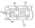
- the method of manufacture of a USB-type electronic keycomprises a stage according to which one starts with a continuous ribbon 54 of the type used in the field of chip cards, based on an engraved or embossed metallic grid.
- the ribbon in the exampleis comprised of a dielectric support film 55 bearing a series of microcircuits or a module 56 each comprising conductive patterns.
- the patternsrepresent contact areas 57 .
- An electronic chipis attached and its contacts are connected electrically by connection wires through wells arranged in the dielectric support. Any other means of connection known in the chip card field may be suitable.
- Protection in the form of application of a drop of insulating resincovers the assembly formed by the chip and the connection wires.
- the dielectricinvolves for example a glass-epoxy film. It comes in the form of a continuous ribbon which can be wound on reels, preferably with lateral perforations 58 for driving the ribbon.
- the ribbonmay be entirely in the form of a fine metal grid in which the patterns are partially pre-cut.
- the methodtherefore employs the same ribbon, in addition to stages of definition of contact areas, if appropriate conductive tracks, chip attachment, connection, coating of the chip, an electrical test and extraction of the module by cutting.
- the contact areas of the moduleare defined in order to correspond to the electrical connection tabs of a USB-type port; i.e. VCC for power supply, another GND for earthing and the two others “D+, D ⁇ ” for data communication.
- the modulealso presents additional contact areas RST, CLK, I/O in order to present ISO-type contacts and allow communication according to the ISO protocol, particularly during the test and/or initialization of the chip and/or during electronic personalization.
- the additional contactsare positioned behind the USB contacts between the USB contacts and the shell or set back in relation to the front of the connector in order to avoid interfering with standard USB connection to a USB port or in order to be subsequently concealed by a shell or other.
- the inventionallows easy personalization (and/or an electrical test and/or initialization) of the modules without modifying the chip card production tool, even between two batches of chip card with the same ISO communication protocol.
- This aspect of the inventionmay be independent from the graphic appearance and the protection envelope, but may contribute to economic production of a key.
- the inventionmay also adapt to USB-type personalization and only electrical contacts in USB format.
- the insulated electronic modulehas been inserted by a “chip card-type” insertion operation in a cavity of a card body 59 in ISO format as in FIG. 1 .
- the cardBefore insertion, the card may comprise decorative graphic printing on one or both of its main faces. This operation may be performed very easily and with optimum quality by chip card technology, unlike keys which have the printing on the shell.
- the card of the inventionmay also comprise a partial pre-cutout 53 of the support 60 in order to facilitate its subsequent extraction, particularly by finger pressure as in FIG. 1 .
- the cardsubsequently receives graphic personalization 61 illustrated by the numbers “12345678”.
- the printingis generally of a decorative nature, such as a decorative background, a table or a pattern, for example.
- the graphic personalizationis generally of an informative nature and may in particular comprise a pattern, a logo, alphanumerical data, a number and barcodes related or unrelated to the data numerically contained on the electronic chip. They may both be made on one or both faces of the card.
- the personalization machineallows association of the electronic and graphic personalization data of the card.
- secret codesmay be associated with data printed on the surface of the body. Different personalizations, at the request of each client or individual, may be made from one support to another in the continuous flow of cards to be printed.
- the support 60comprising the graphic and/or electric personalization is subsequently extracted from the ISO card 59 for its insertion in a shell or casing made of plastic material.
- the extraction operationmay be manual if the support is pre-cut.
- FIG. 5Assembly of the key is illustrated in FIG. 5 .
- the assembly stagesare observed in the order of the arrows (A, B, C, D).
- a shell 61comprising two essential parts: a concave part 62 providing a reception space 63 of a part 52 of the support bearing the graphic printing and a plane 65 or plate protecting the concave part.
- the supportrests completely on the lower shell and the plane extends completely under a front part 51 of the support comprising the contact areas 57 .
- the function of the planeis to supplement the thickness of the support at the level of the contact areas in order to have a total thickness at this level which complies with the USB standard.
- the chip card from which the support is derivedhas a thickness of approximately 0.76 mm, whereas the USB thickness to be achieved is approximately 1.95 mm.
- the supportmay comprise a transverse groove 66 adjacent to the module on its lower face. Its function is to fit into a corresponding rib 67 of the casing located at the junction between the two sub-sections 65 / 62 of the shell and lock the support in position.
- the shelltherefore not only performs a protection function in a single piece via its plane, but also a function of adaptor of the support to the thickness of the USB standard.
- the keymay be used in this manner or if necessary with a USB-type metallic ring (with perforations 69 ) which together encircle the plane and the end of the support.
- the supportmay nevertheless receive conventional protection in the form of film or varnish or a laminated transparent film in order to protect the printing.
- the lower half-shell 61is transparent in order to show another graphic personalization performed on the back of the support. If appropriate, the surface protection is unnecessary since provided by the transparent shell.
- the support 60is itself made of transparent material, particularly ABS, polycarbonate or PET. This makes it possible to perform a single graphic personalization of a single visible side on the front or back of the support through the lower shell; this also makes it possible to create a visual effect by combining the logos printed on the two faces of the support.
- the transparent protection on the keyis preferably performed by an upper half-shell 70 . It is arranged above the support in order to cover a portion of the support, in the present case the rear section of the support outside the contact areas and to fit on to the lower shell and sandwich the support.
- the upper half-shellmay comprise a shoulder 71 of the width of the metallic ring which extends towards the front of the shell.
- the shouldermay for example extend to the limit of the ISO or USB contact areas after mounting on the support.
- the same transparent materialsmay be used.
- the collar or metallic ring 68may then surround/encircle the plane, the shoulder and the contacts in order to ensure an addition hold of the two upper and lower half-shells.
- the upper half-shellmay fit on to the lower half-shell by any appropriate means of attachment. Assembly of the shells may in particular be performed by clipping, gluing, ultrasonic welding, screwing . . .
- additional personalizationmay be performed on the support through the transparent shell, particularly by laser.
- the graphic printing and personalizationare facilitated at several stages of manufacture of the key while guaranteeing their mechanical protection in addition to easy replacement of their protection in case of damage. It is possible to obtain a key with excellent quality of the printing or graphic personalization, particularly in colour at a high resolution, particularly beyond 600 DPI owing to the printing processes commonly used in the chip card field.
- the method and the keyare able to dispense with attachment of the upper shell 67 .
- the adjustment in thicknessperformed by an already assembled one-piece shell, the general shape of which is the same as the shape resulting from the envelope formed by the two half-shells above, but which presents a frontal introduction slit on a front edge between the plane and the shoulder. All that is necessary is to insert the part 52 of the support through the front of the shell in order to perform thickness adjustment of the part 51 with the plane 65 .
- the support and the shellmay respectively comprise additional means of locking them in position in one another, for example hollows/bosses forming a brake to withdrawal of the support from the shell.
- this shelldirectly has the final shape of the key with in particular convex shapes towards the rear facilitating handling or forming part of the aesthetic appearance.
- the front section of the shellmay comprise removable means of the attachment of a protection cap 72 .
- the protection envelopemay comprise only one transparent window 75 arranged on a shell (an opaque shell for example) opposite the graphic personalization of the support.
- the windowmay simply be an opening passing through a shell to the extent that the graphic personalization may comprise a protection film, a laminated film or a transparent coating of the type of those used for chip cards.
- the electronic device obtained, of a USB key type 73can be seen in FIG. 6 .
- Ithas a relatively aesthetic form containing the graphic personalization 60 visible through the transparency of the upper shell.
- the shellmay comprise a perforation or a ring projecting from the shell to accommodate a key ring holder.
- the graphic personalization of the inventionhas the advantage of being indivisible from the electronic circuit or module by means of the same support and of presenting chip card security. Even after replacement of the shell, there is no risk of pairing errors and of breaching the security employed during manufacture of a device presenting a level of security like that of a chip card.
- the graphic printing and/or personalizationis performed on completely standard machines.
- the two transparent plastic shellsare clipped (soldered by ultrasound or glued) around the mini card by means of a manual or readily automatable simple operation.
- the two shellshave means of assembly of the type which can be taken apart.
- This stagedoes not comprise any difficulty, since the entire personalization has already been performed.
- the methodcomprises the following stages in order, according to which an electrical test is performed according to a communication protocol, followed by a decorative graphic, particularly by printing on at least one of the two faces of a moulded or laminated card body with ISO standard dimensions; the module is subsequently glued into a cavity previously arranged in the card body, the card is electronically and graphically personalized and the card body support is extracted.
- One use of the invention envisagedis to have a photograph of the holder or user of the key as a graphic or graphic personalization in order for example to immediately identify the owner of the key.
- the electronic devicealso comprises a transponder function.
- the electronic chipis of the hybrid type for example and comprises a contact-free communication function, of the radiofrequency type for example.
- an antennamay be arranged either in the chip card-type module, or extend in or over the card body or in the part 52 of the support bearing the graphic printing.
- the antennamay preferably extend around the graphic printing on the edge of the body. If necessary, the ring may not be metallic in order to avoid creating a radiofrequency screen to the module antenna.
- the antennamay be connected to the module in a conventional manner to the microcircuit as in hybrid cards with electrical contacts and without contact.
- USB keyapproximately of the width of a personal access swipe card photograph (of at least the face), it was deduced that the key may serve as an identification swipe card and/or a personal access swipe card of the contact-free type.
- the keymay also be used as a secure key for Internet accesses or in order to allow functioning of a secure workstation.
- the printing support and the shellmay be enlarged at the level of the photograph, in order to have for example a support twice as wide as the width of the metallic ring, or three times wider, at the level of the printing.
- the supportmay comprise one or several LED-type diodes connected to the microcircuit and/or antenna in order to indicate activity of communication or transaction or presence of an electromagnetic field or of connection.
- the diodemay be on the surface of the support in the shell or buried in the body of the card. Illumination may be performed through the support body even if non-transparent and visible from the outside. The photo of the individual may in particular be visible by rear illumination of a diode in the card body.
- the printing and/or personalizationmay comprise a photograph of a user and the device may comprise an LED diode in order to illuminate the photograph and/or the printing.
- the LED diodemay be placed in the chip card-type module, connected for example next to the printed circuit chip and coated in such a way that the light diffuses through the card body, with the latter being more or less transparent for example or having a light wave guide function.
- Protective coating of the chip and the LED diodemay be in transparent material.
- the diodemay be supplied in different ways. It may be supplied by the USB port directly or indirectly via a communication chip.
- the antenna of the diodemay be coupled to the main antenna in order to avoid connections to the main antenna RF connected to the chip of the printed circuit.
- the printing of the supportmay be a reflective coating, metallic for example, in order to return the illumination of a diode.
- One applicationwould consist in allowing lighting or a signal by connecting the device to a USB port of a portable object for example having an energy source, such as a portable telephone.
- the inventionmay comprise a method of realization in which the chip comprises several interfaces: a USB interface, a radiofrequency interface RF, an ISO interface if appropriate and a connection for the emitting LED diode if appropriate.
- onemay have the function without radiofrequency contact provided by another contact-free chip connected to an antenna and independent from the first chip.
Landscapes
- Engineering & Computer Science (AREA)
- Computer Hardware Design (AREA)
- Microelectronics & Electronic Packaging (AREA)
- Physics & Mathematics (AREA)
- General Physics & Mathematics (AREA)
- Theoretical Computer Science (AREA)
- Credit Cards Or The Like (AREA)
- Lock And Its Accessories (AREA)
- Circuits Of Receivers In General (AREA)
- Input From Keyboards Or The Like (AREA)
- Supports Or Holders For Household Use (AREA)
- Casings For Electric Apparatus (AREA)
- Purses, Travelling Bags, Baskets, Or Suitcases (AREA)
Abstract
Description
- the envelope comprises a window centered on the graphic printing and/or personalization;
- the support comprises a chip card body containing an electronic module comprising contacts in USB format;
- the lower shell comprises a plane directly below the contacts in order to adapt the thickness of the support to the standard thickness of a USB port;
- the device furthermore comprises ISO-type contacts in addition to an electronic circuit supporting the ISO and USB communication protocols;
- the shell is transparent;
- the method comprises a stage of adaptation of the thickness of the contacts to the thickness of the USB port by means of a plane protecting the lower shell up to the position under the contacts;
- the method comprises the following stages according to which ISO-type contacts are provided on the module and an electronic circuit also capable of supporting an ISO protocol and electronic initialization and/or test and/or personalization is performed according to an ISO communication protocol;
- the support is extracted from the card body.
Claims (22)
Applications Claiming Priority (3)
| Application Number | Priority Date | Filing Date | Title |
|---|---|---|---|
| FR0452494 | 2004-11-02 | ||
| FR0452494AFR2877461B1 (en) | 2004-11-02 | 2004-11-02 | PERSONALIZED ELECTRONIC DEVICE OF THE USB KEY TYPE AND METHOD OF MANUFACTURING SUCH A DEVICE |
| PCT/EP2005/055490WO2007025571A1 (en) | 2004-11-02 | 2005-10-24 | Personalized usb-key type electronic device and method for making same |
Publications (2)
| Publication Number | Publication Date |
|---|---|
| US20080156871A1 US20080156871A1 (en) | 2008-07-03 |
| US7975915B2true US7975915B2 (en) | 2011-07-12 |
Family
ID=34951600
Family Applications (1)
| Application Number | Title | Priority Date | Filing Date |
|---|---|---|---|
| US11/666,753Expired - Fee RelatedUS7975915B2 (en) | 2004-11-02 | 2005-10-24 | Personalized USB-key type electronic device and method for making same |
Country Status (9)
| Country | Link |
|---|---|
| US (1) | US7975915B2 (en) |
| EP (2) | EP1810227B1 (en) |
| JP (1) | JP2008519323A (en) |
| CN (1) | CN101095153A (en) |
| AT (1) | ATE477553T1 (en) |
| DE (1) | DE602005022909D1 (en) |
| ES (1) | ES2350646T3 (en) |
| FR (1) | FR2877461B1 (en) |
| WO (1) | WO2007025571A1 (en) |
Cited By (7)
| Publication number | Priority date | Publication date | Assignee | Title |
|---|---|---|---|---|
| US20130100617A1 (en)* | 2011-02-25 | 2013-04-25 | Huawei Device Co., Ltd. | Connector and Wireless Modem |
| US8649820B2 (en) | 2011-11-07 | 2014-02-11 | Blackberry Limited | Universal integrated circuit card apparatus and related methods |
| USD701864S1 (en) | 2012-04-23 | 2014-04-01 | Blackberry Limited | UICC apparatus |
| USD702240S1 (en) | 2012-04-13 | 2014-04-08 | Blackberry Limited | UICC apparatus |
| US8936199B2 (en) | 2012-04-13 | 2015-01-20 | Blackberry Limited | UICC apparatus and related methods |
| US9311504B2 (en) | 2014-06-23 | 2016-04-12 | Ivo Welch | Anti-identity-theft method and hardware database device |
| US11797817B2 (en) | 2020-08-05 | 2023-10-24 | Smartflex Technology Pte Ltd | Smart cards having LED and methods for fabrication thereof |
Families Citing this family (21)
| Publication number | Priority date | Publication date | Assignee | Title |
|---|---|---|---|---|
| EP1843277A1 (en)* | 2006-04-04 | 2007-10-10 | Axalto SA | USB chip card |
| TWM305951U (en)* | 2006-07-04 | 2007-02-01 | Tai Twun Entpr Co Ltd | Memory card assembling device |
| US20090275844A1 (en) | 2008-05-02 | 2009-11-05 | Masimo Corporation | Monitor configuration system |
| TWM346890U (en)* | 2008-08-19 | 2008-12-11 | Bor Ger Co Ltd | Mini portable memory device |
| FR2936073B1 (en)* | 2008-09-16 | 2015-07-17 | Neowave | PORTABLE OBJECT PROVIDED WITH A GRAPHIC CUSTOMIZATION LOCKED INSIDE ITS HOUSING |
| FR2949011B1 (en) | 2009-08-07 | 2011-09-09 | Emmanuel Thibaudeau | CARD FOR FORMING A COMPUTER ORGAN, AND METHODS OF MANUFACTURING THE SAME AND COMPUTER ORGAN |
| USD624923S1 (en)* | 2009-10-28 | 2010-10-05 | Kingston Technology Corporation | Housing for a portable memory device |
| TW201119882A (en)* | 2009-12-08 | 2011-06-16 | Walton Advanced Eng Inc | Structure with USB memory module. |
| USD625730S1 (en)* | 2009-12-30 | 2010-10-19 | Sanford, L.P. | Receiver |
| USD631884S1 (en)* | 2010-01-19 | 2011-02-01 | Cisco Technology, Inc. | USB set-up key |
| DE202012103759U1 (en)* | 2011-03-14 | 2012-11-09 | Cocos-Promotions Gmbh | Decoration device |
| DE102011112031A1 (en)* | 2011-05-11 | 2012-11-15 | Giesecke & Devrient Gmbh | Method for data exchange between terminal and chip card |
| US8503185B2 (en)* | 2011-07-22 | 2013-08-06 | Ho E Screw & Hardware Co., Ltd. | Bookmark memory stick |
| USD702693S1 (en)* | 2011-11-23 | 2014-04-15 | Digital Hard Copy | Digital storage medium card |
| USD666201S1 (en)* | 2011-11-23 | 2012-08-28 | Digital Hard Copy | Digital storage medium |
| USD702692S1 (en)* | 2011-11-23 | 2014-04-15 | Digital Hard Copy | Card for holding a digital storage medium |
| CN102591835B (en)* | 2011-12-30 | 2014-12-10 | 武汉电信器件有限公司 | Portable downloader |
| USD702695S1 (en)* | 2012-11-08 | 2014-04-15 | Biwin Storage Technology Limited | Memory device |
| CN112823351B (en)* | 2018-10-12 | 2024-06-25 | 里米奇公司 | Automatic storage unit publisher |
| USD1010607S1 (en)* | 2020-11-16 | 2024-01-09 | 3M Innovative Properties Company | Headset |
| CN113823024A (en)* | 2021-11-23 | 2021-12-21 | 云丁网络技术(北京)有限公司 | Smart card identification method, device and system |
Citations (19)
| Publication number | Priority date | Publication date | Assignee | Title |
|---|---|---|---|---|
| JPH09508330A (en) | 1994-02-04 | 1997-08-26 | ギーゼッケ ウント デフリエント ゲーエムベーハー | Data medium having electronic module and method of manufacturing the same |
| JP2002222397A (en) | 2001-01-25 | 2002-08-09 | Dainippon Printing Co Ltd | IC card |
| WO2003027946A1 (en) | 2001-09-24 | 2003-04-03 | Gemplus | Dongle which is intended to be connected to a port of a telecommunications device |
| US20030100203A1 (en) | 2001-11-23 | 2003-05-29 | Power Quotient International Co., Ltd. | Low height USB interface connecting device and a memory storage apparatus thereof |
| US20030107877A1 (en) | 2000-05-03 | 2003-06-12 | Jose Mennecart | Integrated circuit card and case therefor |
| US6594154B1 (en) | 2000-11-06 | 2003-07-15 | Sandisk Corporation | Key chain holders for small electronic circuit cards |
| US20030137859A1 (en) | 2002-01-19 | 2003-07-24 | Norio Sugawara | External storage device |
| JP2003331249A (en) | 2002-05-09 | 2003-11-21 | Carry Computer Engineering Co Ltd | Multi-functional flash memory card structure |
| WO2003105065A1 (en) | 2002-06-11 | 2003-12-18 | Lenscard U.S., Llc | Wallet card with built-in light |
| US6671808B1 (en) | 1999-01-15 | 2003-12-30 | Rainbow Technologies, Inc. | USB-compliant personal key |
| WO2004019261A2 (en) | 2002-08-26 | 2004-03-04 | Dai Nippon Printing Co., Ltd. | Sim, sim holder, ic module, ic card and ic card holder |
| JP2004118771A (en) | 2002-09-30 | 2004-04-15 | Dainippon Printing Co Ltd | SIM holder with USB interface and SIM |
| US20040074264A1 (en) | 2002-10-18 | 2004-04-22 | I/O Interconnect, Inc. | Secure attachment of portable data storage device |
| JP2004133843A (en) | 2002-10-15 | 2004-04-30 | Dainippon Printing Co Ltd | IC module with three types of interfaces, 3-way SIM and SIM holder, 3-way IC card and IC card holder |
| US20040178278A1 (en) | 2003-03-13 | 2004-09-16 | Stmicroelectronics, Inc. | Smart card that can be configured for debugging and software development using secondary communication port |
| US20060046544A1 (en)* | 2004-09-02 | 2006-03-02 | Kyocera Corporation | Card for information equipment, and terminal for information equipment |
| US7269004B1 (en)* | 2005-04-21 | 2007-09-11 | Super Talent Electronics, Inc. | Low-profile USB device |
| US20080276099A1 (en)* | 1999-08-04 | 2008-11-06 | Super Talent Electronics, Inc. | Universal Serial Bus (USB) Flash Drive Having Locking Pins and Locking Grooves for Locking Swivel Cap |
| US20090045802A1 (en)* | 2007-08-13 | 2009-02-19 | Matias Filipe P | Polarity tester for an electronic communication port |
- 2004
- 2004-11-02FRFR0452494Apatent/FR2877461B1/ennot_activeExpired - Fee Related
- 2005
- 2005-10-24WOPCT/EP2005/055490patent/WO2007025571A1/enactiveApplication Filing
- 2005-10-24EPEP05858508Apatent/EP1810227B1/ennot_activeNot-in-force
- 2005-10-24EPEP09169584Apatent/EP2128806A3/ennot_activeCeased
- 2005-10-24ATAT05858508Tpatent/ATE477553T1/ennot_activeIP Right Cessation
- 2005-10-24JPJP2007538397Apatent/JP2008519323A/enactivePending
- 2005-10-24USUS11/666,753patent/US7975915B2/ennot_activeExpired - Fee Related
- 2005-10-24ESES05858508Tpatent/ES2350646T3/enactiveActive
- 2005-10-24DEDE602005022909Tpatent/DE602005022909D1/enactiveActive
- 2005-10-24CNCNA2005800455699Apatent/CN101095153A/enactivePending
Patent Citations (28)
| Publication number | Priority date | Publication date | Assignee | Title |
|---|---|---|---|---|
| US5888624A (en) | 1994-02-04 | 1999-03-30 | Giesecke & Devrient Gmbh | Data carrier with an electronic module and a method for producing the same |
| JPH09508330A (en) | 1994-02-04 | 1997-08-26 | ギーゼッケ ウント デフリエント ゲーエムベーハー | Data medium having electronic module and method of manufacturing the same |
| US6671808B1 (en) | 1999-01-15 | 2003-12-30 | Rainbow Technologies, Inc. | USB-compliant personal key |
| US20080276099A1 (en)* | 1999-08-04 | 2008-11-06 | Super Talent Electronics, Inc. | Universal Serial Bus (USB) Flash Drive Having Locking Pins and Locking Grooves for Locking Swivel Cap |
| US20030107877A1 (en) | 2000-05-03 | 2003-06-12 | Jose Mennecart | Integrated circuit card and case therefor |
| US6594154B1 (en) | 2000-11-06 | 2003-07-15 | Sandisk Corporation | Key chain holders for small electronic circuit cards |
| JP2002222397A (en) | 2001-01-25 | 2002-08-09 | Dainippon Printing Co Ltd | IC card |
| WO2003027946A1 (en) | 2001-09-24 | 2003-04-03 | Gemplus | Dongle which is intended to be connected to a port of a telecommunications device |
| US20040259423A1 (en) | 2001-09-24 | 2004-12-23 | Didier Elbaz | Dongle which is intended to be connected to a port of a telecommunications device |
| US20040029421A1 (en) | 2001-11-23 | 2004-02-12 | Power Quotient International Co., Ltd. | Low height USB interface connecting device and a memory storage apparatus thereof |
| JP2003167646A (en) | 2001-11-23 | 2003-06-13 | Power Quotient Internatl Co Ltd | Low usb interface connecting device and its memory storage device |
| US20030100203A1 (en) | 2001-11-23 | 2003-05-29 | Power Quotient International Co., Ltd. | Low height USB interface connecting device and a memory storage apparatus thereof |
| US20030137859A1 (en) | 2002-01-19 | 2003-07-24 | Norio Sugawara | External storage device |
| JP2003281490A (en) | 2002-01-19 | 2003-10-03 | Sony Corp | External storage device |
| JP2003331249A (en) | 2002-05-09 | 2003-11-21 | Carry Computer Engineering Co Ltd | Multi-functional flash memory card structure |
| DE10233428A1 (en) | 2002-05-09 | 2003-11-27 | Carry Computer Eng Co Ltd | Multiplex chip card has circuitry coupled to contacts that allow transfer of data through a USB or other connection port |
| WO2003105065A1 (en) | 2002-06-11 | 2003-12-18 | Lenscard U.S., Llc | Wallet card with built-in light |
| WO2004019261A2 (en) | 2002-08-26 | 2004-03-04 | Dai Nippon Printing Co., Ltd. | Sim, sim holder, ic module, ic card and ic card holder |
| JP2004118771A (en) | 2002-09-30 | 2004-04-15 | Dainippon Printing Co Ltd | SIM holder with USB interface and SIM |
| JP2004133843A (en) | 2002-10-15 | 2004-04-30 | Dainippon Printing Co Ltd | IC module with three types of interfaces, 3-way SIM and SIM holder, 3-way IC card and IC card holder |
| US20040074264A1 (en) | 2002-10-18 | 2004-04-22 | I/O Interconnect, Inc. | Secure attachment of portable data storage device |
| US20040178278A1 (en) | 2003-03-13 | 2004-09-16 | Stmicroelectronics, Inc. | Smart card that can be configured for debugging and software development using secondary communication port |
| US20040178276A1 (en) | 2003-03-13 | 2004-09-16 | Stmicroelectronics, Inc. | Smart card that can be configured for debugging and software development using secondary communication port |
| JP2004280817A (en) | 2003-03-13 | 2004-10-07 | Stmicroelectronics Inc | Configurable smart card for debugging and software development using secondary communication port |
| US20060046544A1 (en)* | 2004-09-02 | 2006-03-02 | Kyocera Corporation | Card for information equipment, and terminal for information equipment |
| US7269004B1 (en)* | 2005-04-21 | 2007-09-11 | Super Talent Electronics, Inc. | Low-profile USB device |
| US20090045802A1 (en)* | 2007-08-13 | 2009-02-19 | Matias Filipe P | Polarity tester for an electronic communication port |
| US7906956B2 (en)* | 2007-08-13 | 2011-03-15 | Matias Filipe P | Polarity tester for an electronic communication port |
Non-Patent Citations (1)
| Title |
|---|
| English translation of a Decision of Refusal dated Mar. 1, 2011 issued in the corresponding Japanese Patent Application No. 2007-538397. |
Cited By (9)
| Publication number | Priority date | Publication date | Assignee | Title |
|---|---|---|---|---|
| US20130100617A1 (en)* | 2011-02-25 | 2013-04-25 | Huawei Device Co., Ltd. | Connector and Wireless Modem |
| US8649820B2 (en) | 2011-11-07 | 2014-02-11 | Blackberry Limited | Universal integrated circuit card apparatus and related methods |
| USD702240S1 (en) | 2012-04-13 | 2014-04-08 | Blackberry Limited | UICC apparatus |
| USD703208S1 (en) | 2012-04-13 | 2014-04-22 | Blackberry Limited | UICC apparatus |
| US8936199B2 (en) | 2012-04-13 | 2015-01-20 | Blackberry Limited | UICC apparatus and related methods |
| USD701864S1 (en) | 2012-04-23 | 2014-04-01 | Blackberry Limited | UICC apparatus |
| USD702241S1 (en)* | 2012-04-23 | 2014-04-08 | Blackberry Limited | UICC apparatus |
| US9311504B2 (en) | 2014-06-23 | 2016-04-12 | Ivo Welch | Anti-identity-theft method and hardware database device |
| US11797817B2 (en) | 2020-08-05 | 2023-10-24 | Smartflex Technology Pte Ltd | Smart cards having LED and methods for fabrication thereof |
Also Published As
| Publication number | Publication date |
|---|---|
| US20080156871A1 (en) | 2008-07-03 |
| DE602005022909D1 (en) | 2010-09-23 |
| ES2350646T3 (en) | 2011-01-25 |
| EP2128806A3 (en) | 2012-07-04 |
| CN101095153A (en) | 2007-12-26 |
| FR2877461B1 (en) | 2007-05-18 |
| WO2007025571A1 (en) | 2007-03-08 |
| JP2008519323A (en) | 2008-06-05 |
| EP1810227A1 (en) | 2007-07-25 |
| FR2877461A1 (en) | 2006-05-05 |
| EP2128806A2 (en) | 2009-12-02 |
| ATE477553T1 (en) | 2010-08-15 |
| EP1810227B1 (en) | 2010-08-11 |
Similar Documents
| Publication | Publication Date | Title |
|---|---|---|
| US7975915B2 (en) | Personalized USB-key type electronic device and method for making same | |
| US12254367B2 (en) | Metal, ceramic, or ceramic-coated transaction card with window or window pattern and optional backlighting | |
| US10783426B2 (en) | Dual-interface metal hybrid smartcard | |
| EP1535240B1 (en) | Sim, ic module and ic card | |
| US8162696B2 (en) | Dongle which is intended to be connected to a port of a telecommunications device | |
| KR102210842B1 (en) | Improved lightable card | |
| JP2005530228A (en) | Wallet card with built-in light | |
| US11618191B2 (en) | DI metal transaction devices and processes for the manufacture thereof | |
| US7121473B2 (en) | Security memory card and production method | |
| EP4260233B1 (en) | Method for manufacturing a smart card with positioning of a metal insert | |
| AU2021216452B2 (en) | Di metal transaction devices and processes for the manufacture thereof | |
| JP4240977B2 (en) | SIM holder with USB interface and SIM | |
| EP4094190B1 (en) | Metal, ceramic, or ceramic-coated transaction card with window or window pattern and optional backlighting | |
| CN1902642B (en) | Usb electronic key | |
| US20110049248A1 (en) | Electronic Device Comprising a Microcircuit Card |
Legal Events
| Date | Code | Title | Description |
|---|---|---|---|
| AS | Assignment | Owner name:GEMPLUS, FRANCE Free format text:ASSIGNMENT OF ASSIGNORS INTEREST;ASSIGNORS:FIDALGO, JEAN-CHRISTOPHE;BIREMONT, JEAN-CHARLES;DOSSETTO, LUCILE;AND OTHERS;REEL/FRAME:021491/0610;SIGNING DATES FROM 20050721 TO 20050805 Owner name:GEMPLUS, FRANCE Free format text:ASSIGNMENT OF ASSIGNORS INTEREST;ASSIGNORS:FIDALGO, JEAN-CHRISTOPHE;BIREMONT, JEAN-CHARLES;DOSSETTO, LUCILE;AND OTHERS;SIGNING DATES FROM 20050721 TO 20050805;REEL/FRAME:021491/0610 | |
| AS | Assignment | Owner name:GEMALTO SA, FRANCE Free format text:MERGER;ASSIGNOR:GEMPLUS;REEL/FRAME:026305/0304 Effective date:20081001 | |
| STCF | Information on status: patent grant | Free format text:PATENTED CASE | |
| FPAY | Fee payment | Year of fee payment:4 | |
| MAFP | Maintenance fee payment | Free format text:PAYMENT OF MAINTENANCE FEE, 8TH YEAR, LARGE ENTITY (ORIGINAL EVENT CODE: M1552); ENTITY STATUS OF PATENT OWNER: LARGE ENTITY Year of fee payment:8 | |
| FEPP | Fee payment procedure | Free format text:MAINTENANCE FEE REMINDER MAILED (ORIGINAL EVENT CODE: REM.); ENTITY STATUS OF PATENT OWNER: LARGE ENTITY | |
| LAPS | Lapse for failure to pay maintenance fees | Free format text:PATENT EXPIRED FOR FAILURE TO PAY MAINTENANCE FEES (ORIGINAL EVENT CODE: EXP.); ENTITY STATUS OF PATENT OWNER: LARGE ENTITY | |
| STCH | Information on status: patent discontinuation | Free format text:PATENT EXPIRED DUE TO NONPAYMENT OF MAINTENANCE FEES UNDER 37 CFR 1.362 | |
| FP | Lapsed due to failure to pay maintenance fee | Effective date:20230712 |