US7975155B2 - Apparatus and method for controlling voltage and frequency - Google Patents
Apparatus and method for controlling voltage and frequencyDownload PDFInfo
- Publication number
- US7975155B2 US7975155B2US11/575,002US57500208AUS7975155B2US 7975155 B2US7975155 B2US 7975155B2US 57500208 AUS57500208 AUS 57500208AUS 7975155 B2US7975155 B2US 7975155B2
- Authority
- US
- United States
- Prior art keywords
- clock signal
- voltage level
- hardware module
- average load
- signal frequency
- Prior art date
- Legal status (The legal status is an assumption and is not a legal conclusion. Google has not performed a legal analysis and makes no representation as to the accuracy of the status listed.)
- Expired - Fee Related, expires
Links
Images


Classifications
- G—PHYSICS
- G06—COMPUTING OR CALCULATING; COUNTING
- G06F—ELECTRIC DIGITAL DATA PROCESSING
- G06F1/00—Details not covered by groups G06F3/00 - G06F13/00 and G06F21/00
- G06F1/26—Power supply means, e.g. regulation thereof
- G06F1/32—Means for saving power
- G06F1/3203—Power management, i.e. event-based initiation of a power-saving mode
- G06F1/3234—Power saving characterised by the action undertaken
- G06F1/324—Power saving characterised by the action undertaken by lowering clock frequency
- G—PHYSICS
- G06—COMPUTING OR CALCULATING; COUNTING
- G06F—ELECTRIC DIGITAL DATA PROCESSING
- G06F1/00—Details not covered by groups G06F3/00 - G06F13/00 and G06F21/00
- G06F1/26—Power supply means, e.g. regulation thereof
- G06F1/32—Means for saving power
- G06F1/3203—Power management, i.e. event-based initiation of a power-saving mode
- G06F1/3234—Power saving characterised by the action undertaken
- G06F1/3296—Power saving characterised by the action undertaken by lowering the supply or operating voltage
- Y—GENERAL TAGGING OF NEW TECHNOLOGICAL DEVELOPMENTS; GENERAL TAGGING OF CROSS-SECTIONAL TECHNOLOGIES SPANNING OVER SEVERAL SECTIONS OF THE IPC; TECHNICAL SUBJECTS COVERED BY FORMER USPC CROSS-REFERENCE ART COLLECTIONS [XRACs] AND DIGESTS
- Y02—TECHNOLOGIES OR APPLICATIONS FOR MITIGATION OR ADAPTATION AGAINST CLIMATE CHANGE
- Y02D—CLIMATE CHANGE MITIGATION TECHNOLOGIES IN INFORMATION AND COMMUNICATION TECHNOLOGIES [ICT], I.E. INFORMATION AND COMMUNICATION TECHNOLOGIES AIMING AT THE REDUCTION OF THEIR OWN ENERGY USE
- Y02D10/00—Energy efficient computing, e.g. low power processors, power management or thermal management
Definitions
- the present inventionrelates to apparatuses and methods for controlling supply voltage and clock signal frequency within a processor based device and.
- Mobile devicessuch as but not limited to personal data appliances, cellular phones, radios, pagers, lap top computers, and the like are required to operate for relatively long periods before being recharged. These mobile devices usually include one or more processors as well as multiple memory modules and other peripheral devices.
- a first techniqueincludes reducing the clock frequency of the mobile device.
- a second techniqueis known as dynamic voltage scaling (DVS) or alternatively is known as dynamic voltage and frequency scaling (DVFS) and includes altering the voltage that is supplied to a processor as well as altering the frequency of a clock signal that is provided to the processor in response to the computational load demands (also referred to as throughput) of the processor.
- VFSdynamic voltage scaling
- DVFSdynamic voltage and frequency scaling
- Higher voltage levelsare associated with higher operating frequencies and higher computational load but are also associated with higher energy consumption.
- DVScan be implemented by software.
- a disadvantage of software based applicationresults from timing issues and the computational load that an execution of such software imposes on a processor.
- DVScan also be implemented by hardware.
- a disadvantage of hardware-based solutionresides on their inflexibility and complexity.
- the inventionprovides a method and an apparatus for controlling voltage level and clock signal frequency supplied to a system.
- the apparatusincludes a hardware module, adapted to receive at least one activity related signal representative of an activity of at least one component of the system and to determine a voltage level and a clock signal frequency to be provided to the system, and a software module, adapted to configure a voltage source and a clock signal source in response to the determination.
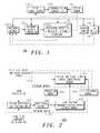
- FIG. 1is a schematic illustration of a system according to an embodiment of the invention
- FIG. 2illustrates an apparatus, according to an embodiment of the invention
- FIG. 3is a schematic diagram of various modules of an apparatus, according to an embodiment of the invention.
- FIG. 4is a flow chart of a method for
- FIG. 1is a schematic illustration of a system 100 that includes multiple components such as processor 110 , memory bank 120 , I/O modules 130 , interrupt request controller 140 , clock signal source 220 , voltage source 210 , synchronization control unit 230 .
- System 100also includes a hardware module 200 .
- processor 110executes a software module 300 that with the hardware module 200 forms apparatus 232 .
- system 100can have various configurations and that the components illustrated in FIG. 1 represent only a single exemplary configuration of system 100 .
- system 100is includes within a mobile device such as a cellular phone.
- the hardware module 200is adapted to receive one or more activity related signals representative of an activity of at least one component of the system 100 and in response determine whether to alter the voltage/frequency provided to the components of system 100 .
- activity related signalsmay include, for example, memory access signals (read/write), cache hit/miss signals, bus related signals, processor IDLE signal, various processor instructions, interrupt requests, I/O access, and the like.
- Apparatus 232is capable of determining the supply voltage and clock signal frequency supplied to system 100 (said characteristic pair is referred to as voltage/frequency) under various timing constraints that include, for example: the decision period of apparatus 232 , voltage supply and clock signal supply stabilization period, and system's 100 and especially processor's 110 load change rate.
- the voltage/frequencyWhen the load of system 100 increases, the voltage/frequency must be increased relatively fast in order to prevent performance penalties that are especially critical when the system 100 executes a real time program such as a video processing program.
- the apparatus 232In both cases the apparatus 232 must track the load of system 100 in a relatively fast manner but without introducing too many voltage/frequency changes.
- the apparatus 232can be adapted to apply a first policy when deciding to increase the frequency/voltage supplied to system 100 and a second policy, that conveniently differs from the first policy, when deciding to decrease the voltage/frequency supplied to system 100 . It is noted that apparatus 232 can apply various policies, even the same or substantially the same policies when deciding to increase or decrease the supplied voltage/frequency.
- applying different voltage/frequency increment and decrement policiesare implemented, for example, by setting different average load thresholds (Nup and Ndown, Lp and Ldown) to various load related events.
- Nup and Ndown, Lp and Ldownaverage load thresholds
- Those of skill in the artwill appreciate that using the same (or substantially the same) voltage/frequency increment and decrement policies can include using the same average load thresholds, but this is not necessarily so.
- FIG. 2illustrates apparatus 232 , according to an embodiment of the invention.
- the various tasks associated with controlling and providing voltage and clock signals to system 100were divided between the hardware module 200 and the software module 300 of apparatus 232 .
- the hardware module 200receives one or usually multiple activity related signals, applies a load tracking algorithm such as but not limited to the exponential moving average (EMA) algorithm and determine when to alter the voltage/frequency supplied to system 100 .
- EMAexponential moving average
- the software module 300configures the voltage source 210 and the clock signal source 220 .
- the apparatus 232includes a prediction module 520 that predicts how to alter the voltage/frequency in response to previous exponential moving average load estimates.
- the hardware module 200includes programmable components thus allowing alterations of the decision process.
- the control of the voltage source 210 and clock signal source 220is relatively simple and does not load the processor 110 . Furthermore, its simplicity allows components having limited processing capabilities, such as DMA modules and simple controllers, to execute the voltage and clock signal source configuration module 310 . In addition, various existing processors have the capability of setting voltage and clock signal frequency, thus utilizing this capability further increases the efficiency of apparatus 232 and system 100 as a whole.
- the apparatus 232samples the activity related signals by the clock signal CLK supplied to the system or by a clock signal having a lower frequency, such as CLK_ 3 that is a derivative of CLK.
- Said samplingprovides a more accurate load level tracking than a system that uses a real time clock that is not influenced by the changes of clock signals provided to the monitored system.
- System 100receives a supply voltage V(t) as well as a clock signal CLK of a certain frequency F(t) from a synchronization control unit 230 that synchronizes the levels of V(t) and F(t) such as to prevent, for example, a case in which the supplied voltage V(t) does not allow the system 100 to operate at a the frequency F(t) of the clock signal.
- the synchronization control unit 230is connected to a clock signal source 220 for receiving the clock signal and is also connected to a voltage source 210 for receiving the supply voltage.
- the clock signal source 220includes two phase locked loops, whereas while one is supplying a current clock signal of a current frequency the other can be tuned to supply the next clock signal having a next frequency.
- the voltage sourcecan also include two voltage sources but this is not necessarily so.
- Apparatus 232includes a hardware module 200 that includes a system/processor load tracking unit 402 , a processing module 404 and a load tracking frequency/voltage update request module 406 .
- the software module 300includes a voltage and clock signal source configuration module 310 .
- FIG. 2also illustrates two optional modules such as prediction module 520 and user configures module 530 , each can be a hardware module, a software module or a combination of both hardware and software.
- the voltage and clock signal source configuration module 310is capable of configuring the clock signal source 220 as well as the voltage source 210 by various prior art methods, such as writing control values to registers accessed by these sources.
- the voltage and clock signal source configuration module 310is capable of receiving a requests to alter the voltage/frequency from load tracking frequency/voltage update request module 406 and to convert the request to a format that can be understood by and accessible to the clock signal source 220 as well as the voltage source 210 .
- the voltage and clock signal source configuration module 310receives also a request to alter the voltage/frequency from a prediction module 520 .
- the voltage and clock signal source configuration module 310is also adapted to receive requests from a user-configured module 530 .
- requestscan be provided to the voltage and clock signal source configuration module 310 from more that a single module it may apply various decision processes to decide how to alter the voltage/frequency.
- Each requestcan be assigned with a certain priority and/or weight and any combination of at least one of the requests can be applied.
- a request of the prediction module 520can override a request of the load tracking frequency/voltage update request module 406 , and a request from the user-configured module 530 can override both.
- System/processor load tracking unit 402received multiple activity related signal and is capable of assigning a predefined weight to each signal. Conveniently, the system/processor load tracking unit 402 tracks the activity of the processor 100 by monitoring at least one signal such as an IDLE signal and also is also capable of tracking the activity of other components of system.
- the a system/processor load tracking module 402provides an indication of the activities of various components to a processing module 404 that outputs a load indication and an exponential moving average load estimate to the load tracking frequency/voltage update request module 406 and also provides the exponential moving average load estimate to the prediction module 520 .
- FIG. 3is a schematic diagram of various modules 402 - 406 of the apparatus 232 , according to an embodiment of the invention.
- System/processor load tracking module 402includes modules 410 and 430 .
- Processor load sampling module 410samples the IDLE or NON-IDLE (BUSY) signal of processor 110 .
- the IDLE or NON-IDLE (BUSY) signalis sampled by CLK and creates IDLE′ sampled signal.
- Thes IDLE′ sampled signalis provided to a processor load pre-averaging module 420 that belongs to processing module 404 .
- the processor load pre-averaging module 420calculates a ratio R between the amounts of clock signals (CLK) during a certain averaging period and between the amount of sampled signal IDLE′ provided by processor load sampling module 410 during that certain averaging period.
- the length of the averaging periodis programmable. Conveniently, either module 410 or module 420 can multiple either IDLE′ or R by a programmable weight W_IDLE. Conveniently, the averaging periods do not overlap, but this is not necessarily so.
- processor load pre-averaging module 420also divides CLK to generate a slower clock signal CLK_ 3 that is provided to various modules such as modules 430 and 440 - 490 .
- System load sampling and weighting module 430receives multiple activity related signals from other components of system 100 , although it can also receive one or more signals (other than IDLE) from processor 110 .
- the system load sampling and weighting module 430samples the received signals by CLK_ 3 and multiplies each sampled activity related signal by a corresponding programmable weight to provide multiple weighted system activity related signals SL_ 1 -SL_K.
- Ris also provided to a log buffer 560 , and conveniently said log buffer 560 can also receive at least one of the load indication system load indication signals.
- Processing module 404includes modules 420 , 440 and 450 .
- Adder module 440adds R to the multiple weighted system activity related signals SL_ 1 -SL_K to provide a load indication LL(t).
- the load indication LL(t)is provided to a bypass module 500 as well to a exponential moving average (EMA) module 450 .
- EMAexponential moving average
- the EMA module 450applies an exponential moving average module algorithm that is responsive to at least one programmable parameter ⁇ .
- ⁇ tis responsive to CLK_ 3 and to an amount of clock cycles required for the calculation of EMA(t).
- the inventorsused an eight bit ⁇ , but this is not necessarily so.
- ⁇is increased the current value of LL(t) is more dominant thus rapid changes of LL(t) can be tracked.
- ⁇is decreased previous samples are more relevant and a more stable tracking process is achieved.
- Load tracking frequency/voltage update request module 406includes modules 460 - 480 .
- Load tracking frequency/voltage update request module 406is adapted to apply different voltage/frequency increment and decrement policies. These different policies are applied by setting different thresholds like Lup and Ldown as well as using two different counters for counting consecutive EMA_higher_than_Lup signals and EMA_lower_than_Ldown signals. According to another embodiment of the invention the load tracking frequency/voltage update request can apply the same (or substantially the same) policies, for example by using a single threshold instead of using a lower threshold and an upper threshold, but this is not necessarily so.
- Load tracking frequency/voltage update request module 406receives exponential moving average load estimate EMA(t) and compares it in parallel to a upper average load threshold Lup and to a lower average load threshold Ldown. Both load thresholds are programmable. Higher Lup values lead to a slower voltage/frequency update process while lower Ldown values lead to an unstable voltage/frequency update process.
- the dual threshold comparison module 460Each time EMA(t) exceeds Lup the dual threshold comparison module 460 generates a EMA_higher_than_Lup signal.
- the EMA_higher_than_Lup signalis sent to a first counter module 470 that counts the amount of consecutive EMA_higher_than_Lup signals.
- the first counter module 470generates a request to increase the voltage/frequency (Req_up(t)) if more than a programmable amount (N_up) of consequent EMA_higher_than_Lup signals were received.
- the dual threshold comparison module 460Each time EMA(t) is below Ldown the dual threshold comparison module 460 generates a EMA_lower_than_Ldown signal.
- the EMA_lower_than_Ldown signalis sent to a second counter module 480 that counts the amount of consecutive EMA_lower_than_Ldown signals.
- the second counter module 480generates a request to decrease the voltage/frequency (Req_down(t)) if more than a programmable amount (N_down) of consequent EMA_lower_than_Ldown signals were received.
- Req_up(t) and Req_down(t) signalsare provided to interfacing logic 490 that sets various status bits, accessible by software module 300 , to reflect a received request to alter voltage/frequency.
- Interfacing logiccan also send a request to interrupt request controller 140 (or directly to processor 110 ) to initiate an interrupt request that enables processor 110 to execute voltage and clock signal source configuration module 310 .
- the voltage and clock signal source configuration module 310converts requests to increase or decrease voltage/frequency to commands that control the clock signal source 220 and the voltage source 210 accordingly.
- the bypass module 500receives LL(t) and compares it to a predefined load threshold. If said load threshold is exceeded the bypass module 500 can send a request to increase the voltage/frequency to interfacing logic 490 , regardless of the output of modules 450 - 480 .
- the bypass module 500allows the apparatus 232 to respond quickly to sudden system overload situations.
- the prediction module 520can predict power consumption based upon previously stored load indications, for example the load indications stored at the log buffer 560 .
- the prediction module 520can response to instructions being executed by processor 100 . For example, it may predict the load when processor 110 executes loops, by monitoring various commands, flow changes an/or loop commands fetched by processor 110 .
- the prediction module 520can include software components, hardware components or a combination of both.
- the programmable values provided to the apparatus 232can be responsive to previously provided values and even to the tasks that are executes by system 100 and especially processor 110 .
- system 100mainly processes video
- the system 100 and especially processor 110can load a first set of programmable values to the apparatus 232 , while when executing other tasks, another set of programmable values can be loaded.
- the programmable valuescan be also programmed in response to previous voltage/frequency alterations. For example very frequent voltage/frequency alterations can indicate that a slower tracking process is required and vice verse.
- the programmable valuescan also be responsive to other parameters such as operating conditions (such as temperature, battery level) of system 100 and the like.
- FIG. 4is a flow chart of a method 600 for controlling voltage level and clock signal frequency supplied to a system.
- Method 600starts by stage 610 of receiving, at a hardware module, at least one activity related signal.
- stage 610includes assigning a weight to each activity related signal.
- the processor load sampling module 410 and the system load sampling and weighting module 430receive multiple signals representative of the activities of various components of system 100 including processor 110 .
- Stage 610is followed by stage 620 of determining, by the hardware module, a voltage level and a clock signal frequency to be provided to the system.
- stage 620includes calculating an exponential moving average load estimate.
- the exponential moving average load estimateis compared to an upper average load threshold and to a lower average load threshold.
- said determinationis responsive to a calculation process applied by modules 420 - 480 .
- the methodcan include applying the same (or substantially the same) voltage/frequency policies, for example by using a single threshold instead of using an lower average threshold and an upper average threshold, but this is not necessarily so.
- stage 620further includes comparing a load indication to a load threshold and generating a request to increase the voltage level and clock signal frequency if the load indication exceeds the load threshold.
- this stagecan be implemented by bypass module 500 .
- stage 620is followed by a stage of storing load indications.
- stage 620includes estimating future load in response to the stored load indications.
- the hardware moduleapplies a first policy for increasing the voltage level and clock signal frequency and a second policy for decreasing the voltage level and clock signal frequency.
- Stage 620is followed by stage 630 of configuring, by a software module, a voltage source and a clock signal source in response to the determination.
- method 600includes providing the clock signal to a first portion of the hardware module and providing another clock signal of a lower frequency to a second portion of the hardware module.
- method 600includes programming at least one programmable parameter of the hardware module.
Landscapes
- Engineering & Computer Science (AREA)
- Theoretical Computer Science (AREA)
- Physics & Mathematics (AREA)
- General Engineering & Computer Science (AREA)
- General Physics & Mathematics (AREA)
- Power Sources (AREA)
Abstract
Description
Claims (16)
Applications Claiming Priority (1)
| Application Number | Priority Date | Filing Date | Title |
|---|---|---|---|
| PCT/IB2004/004473WO2006056824A2 (en) | 2004-09-10 | 2004-09-10 | Apparatus and method for controlling voltage and frequency |
Publications (2)
| Publication Number | Publication Date |
|---|---|
| US20090144572A1 US20090144572A1 (en) | 2009-06-04 |
| US7975155B2true US7975155B2 (en) | 2011-07-05 |
Family
ID=36288631
Family Applications (1)
| Application Number | Title | Priority Date | Filing Date |
|---|---|---|---|
| US11/575,002Expired - Fee RelatedUS7975155B2 (en) | 2004-09-10 | 2004-09-10 | Apparatus and method for controlling voltage and frequency |
Country Status (2)
| Country | Link |
|---|---|
| US (1) | US7975155B2 (en) |
| WO (1) | WO2006056824A2 (en) |
Cited By (5)
| Publication number | Priority date | Publication date | Assignee | Title |
|---|---|---|---|---|
| US20080141047A1 (en)* | 2004-09-10 | 2008-06-12 | Freescale Semiconductor, Inc. | Apparatus and Method for Controlling Voltage and Frequency |
| US20100218019A1 (en)* | 2007-10-09 | 2010-08-26 | St-Ericsson Sa | Non-recursive adaptive filter for predicting the mean processing performance of a complex system's processing core |
| US20100299545A1 (en)* | 2009-05-20 | 2010-11-25 | Samsung Electronics Co., Ltd. | Methods of power management and apparatus thereof |
| US20110173617A1 (en)* | 2010-01-11 | 2011-07-14 | Qualcomm Incorporated | System and method of dynamically controlling a processor |
| US20150241859A1 (en)* | 2012-10-18 | 2015-08-27 | Mitsubishi Electric Corporation | Management device, management system, management method, and program |
Families Citing this family (15)
| Publication number | Priority date | Publication date | Assignee | Title |
|---|---|---|---|---|
| WO2007049100A1 (en)* | 2005-10-27 | 2007-05-03 | Freescale Semiconductor, Inc. | System and method for controlling voltage level and clock frequency supplied to a system |
| CN100561404C (en)* | 2005-12-29 | 2009-11-18 | 联想(北京)有限公司 | Ways to Save Processor Power |
| WO2007148159A1 (en)* | 2006-06-22 | 2007-12-27 | Freescale Semiconductor, Inc. | A method and device for power management |
| WO2008015495A1 (en)* | 2006-08-03 | 2008-02-07 | Freescale Semiconductor, Inc. | Device and method for power management |
| US8296121B2 (en)* | 2007-04-25 | 2012-10-23 | Cadence Design Systems, Inc. | Method and apparatus for controlling power in an emulation system |
| EP2294499A1 (en)* | 2008-06-25 | 2011-03-16 | Nxp B.V. | Electronic device, a method of controlling an electronic device, and system on-chip |
| EP2307940A1 (en)* | 2008-07-23 | 2011-04-13 | Nxp B.V. | Adjustment of a processor frequency |
| GB2476606B (en) | 2008-09-08 | 2012-08-08 | Virginia Tech Intell Prop | Systems, devices, and methods for managing energy usage |
| US8700934B2 (en)* | 2010-07-27 | 2014-04-15 | Blackberry Limited | System and method for dynamically configuring processing speeds in a wireless mobile telecommunications device |
| US8954017B2 (en)* | 2011-08-17 | 2015-02-10 | Broadcom Corporation | Clock signal multiplication to reduce noise coupled onto a transmission communication signal of a communications device |
| US8966300B2 (en)* | 2011-10-04 | 2015-02-24 | Ericsson Modems Sa | DFVS-enabled multiprocessor |
| US9436265B2 (en)* | 2013-10-24 | 2016-09-06 | Fujitsu Limited | Information processing apparatus and load control method |
| US20150309552A1 (en)* | 2014-04-25 | 2015-10-29 | Qualcomm Innovation Center, Inc. | Enhancement in linux ondemand governor for periodic loads |
| US9244123B1 (en) | 2014-11-25 | 2016-01-26 | Freescale Semiconductor, Inc. | Synchronous circuit, method of designing a synchronous circuit, and method of validating a synchronous circuit |
| CN117492552B (en)* | 2024-01-03 | 2024-04-16 | 芯瞳半导体技术(山东)有限公司 | Dynamic voltage frequency adjustment method, controller, device, equipment and storage medium |
Citations (11)
| Publication number | Priority date | Publication date | Assignee | Title |
|---|---|---|---|---|
| US6192479B1 (en) | 1995-01-19 | 2001-02-20 | Texas Instruments Incorporated | Data processing with progressive, adaptive, CPU-driven power management |
| US20020099964A1 (en) | 2001-01-22 | 2002-07-25 | Andrej Zdravkovic | Reducing power consumption by estimating engine load and reducing engine clock speed |
| US20020133729A1 (en)* | 2001-03-19 | 2002-09-19 | Guy Therien | Method for determining transition points on multiple performance state capable microprocessors |
| US6574739B1 (en) | 2000-04-14 | 2003-06-03 | Compal Electronics, Inc. | Dynamic power saving by monitoring CPU utilization |
| US20030110423A1 (en) | 2001-12-11 | 2003-06-12 | Advanced Micro Devices, Inc. | Variable maximum die temperature based on performance state |
| US6584571B1 (en) | 1990-06-01 | 2003-06-24 | St. Clair Intellectual Property Consultants, Inc. | System and method of computer operating mode clock control for power consumption reduction |
| US20030125900A1 (en) | 2002-01-02 | 2003-07-03 | Doron Orenstien | Deterministic power-estimation for thermal control |
| US20050044429A1 (en) | 2003-08-22 | 2005-02-24 | Ip-First Llc | Resource utilization mechanism for microprocessor power management |
| US7058824B2 (en)* | 2001-06-15 | 2006-06-06 | Microsoft Corporation | Method and system for using idle threads to adaptively throttle a computer |
| US7360100B2 (en)* | 2003-08-01 | 2008-04-15 | Ge Medical Systems Global Technology Company, Llc | Intelligent power management control system and method |
| US20080141047A1 (en)* | 2004-09-10 | 2008-06-12 | Freescale Semiconductor, Inc. | Apparatus and Method for Controlling Voltage and Frequency |
Family Cites Families (1)
| Publication number | Priority date | Publication date | Assignee | Title |
|---|---|---|---|---|
| JP2001298008A (en)* | 2000-04-14 | 2001-10-26 | Sony Corp | Method and device for polishing |
- 2004
- 2004-09-10USUS11/575,002patent/US7975155B2/ennot_activeExpired - Fee Related
- 2004-09-10WOPCT/IB2004/004473patent/WO2006056824A2/enactiveApplication Filing
Patent Citations (12)
| Publication number | Priority date | Publication date | Assignee | Title |
|---|---|---|---|---|
| US6584571B1 (en) | 1990-06-01 | 2003-06-24 | St. Clair Intellectual Property Consultants, Inc. | System and method of computer operating mode clock control for power consumption reduction |
| US6192479B1 (en) | 1995-01-19 | 2001-02-20 | Texas Instruments Incorporated | Data processing with progressive, adaptive, CPU-driven power management |
| US6574739B1 (en) | 2000-04-14 | 2003-06-03 | Compal Electronics, Inc. | Dynamic power saving by monitoring CPU utilization |
| US20020099964A1 (en) | 2001-01-22 | 2002-07-25 | Andrej Zdravkovic | Reducing power consumption by estimating engine load and reducing engine clock speed |
| US20020133729A1 (en)* | 2001-03-19 | 2002-09-19 | Guy Therien | Method for determining transition points on multiple performance state capable microprocessors |
| WO2002074046A2 (en) | 2001-03-19 | 2002-09-26 | Intel Corporation | A method for determining transition points on multiple performance state capable microprocessors |
| US7058824B2 (en)* | 2001-06-15 | 2006-06-06 | Microsoft Corporation | Method and system for using idle threads to adaptively throttle a computer |
| US20030110423A1 (en) | 2001-12-11 | 2003-06-12 | Advanced Micro Devices, Inc. | Variable maximum die temperature based on performance state |
| US20030125900A1 (en) | 2002-01-02 | 2003-07-03 | Doron Orenstien | Deterministic power-estimation for thermal control |
| US7360100B2 (en)* | 2003-08-01 | 2008-04-15 | Ge Medical Systems Global Technology Company, Llc | Intelligent power management control system and method |
| US20050044429A1 (en) | 2003-08-22 | 2005-02-24 | Ip-First Llc | Resource utilization mechanism for microprocessor power management |
| US20080141047A1 (en)* | 2004-09-10 | 2008-06-12 | Freescale Semiconductor, Inc. | Apparatus and Method for Controlling Voltage and Frequency |
Non-Patent Citations (3)
| Title |
|---|
| Final Office Action mailed Oct. 25, 2010 for U.S. Appl. No. 11/575,004, 12 pages. |
| Govil et al; "Comparing Algorithms for Dynamic Speed-Setting of a Low-Power CPU"; International Computer Science Institute, Berkeley, CA, Apr. 1995. |
| Non-Final Office Action mailed Apr. 15, 2010 for U.S. Appl. No. 11/575,004, 13 pages. |
Cited By (9)
| Publication number | Priority date | Publication date | Assignee | Title |
|---|---|---|---|---|
| US20080141047A1 (en)* | 2004-09-10 | 2008-06-12 | Freescale Semiconductor, Inc. | Apparatus and Method for Controlling Voltage and Frequency |
| US20100218019A1 (en)* | 2007-10-09 | 2010-08-26 | St-Ericsson Sa | Non-recursive adaptive filter for predicting the mean processing performance of a complex system's processing core |
| US20100299545A1 (en)* | 2009-05-20 | 2010-11-25 | Samsung Electronics Co., Ltd. | Methods of power management and apparatus thereof |
| US8245057B2 (en)* | 2009-05-20 | 2012-08-14 | Samsung Electronics Co., Ltd. | Method of power management for dynamically controlling power in a processor in according to a workload rate of the processor |
| US20110173617A1 (en)* | 2010-01-11 | 2011-07-14 | Qualcomm Incorporated | System and method of dynamically controlling a processor |
| US8671413B2 (en) | 2010-01-11 | 2014-03-11 | Qualcomm Incorporated | System and method of dynamic clock and voltage scaling for workload based power management of a wireless mobile device |
| US8996595B2 (en)* | 2010-01-11 | 2015-03-31 | Qualcomm Incorporated | User activity response dynamic frequency scaling processor power management system and method |
| US20150241859A1 (en)* | 2012-10-18 | 2015-08-27 | Mitsubishi Electric Corporation | Management device, management system, management method, and program |
| US10310460B2 (en)* | 2012-10-18 | 2019-06-04 | Mitsubishi Electric Corporation | Management device, management system, management method, and program |
Also Published As
| Publication number | Publication date |
|---|---|
| US20090144572A1 (en) | 2009-06-04 |
| WO2006056824A3 (en) | 2006-07-27 |
| WO2006056824A2 (en) | 2006-06-01 |
Similar Documents
| Publication | Publication Date | Title |
|---|---|---|
| US8135966B2 (en) | Method and device for power management | |
| US7975155B2 (en) | Apparatus and method for controlling voltage and frequency | |
| US7143203B1 (en) | Storage device control responsive to operational characteristics of a system | |
| USRE48819E1 (en) | Performance and power optimization via block oriented performance measurement and control | |
| CN107678855B (en) | Processor dynamic adjustment method, device and processor chip | |
| US8261112B2 (en) | Optimizing power consumption by tracking how program runtime performance metrics respond to changes in operating frequency | |
| EP0730217B1 (en) | Power conservation and thermal management arrangements for computers | |
| US9292068B2 (en) | Controlling a turbo mode frequency of a processor | |
| CN101379453B (en) | Method and apparatus for using dynamic workload characteristics to control CPU frequency and voltage scaling | |
| US8935549B2 (en) | Microprocessor with multicore processor power credit management feature | |
| US9104411B2 (en) | System and method for controlling central processing unit power with guaranteed transient deadlines | |
| JP2007128556A (en) | Method and system for controlling computer operation in response to cpu operating characteristic | |
| US20080141047A1 (en) | Apparatus and Method for Controlling Voltage and Frequency | |
| US20080049009A1 (en) | Dynamic clock control circuit and method | |
| US8224497B2 (en) | Energy limit in a sliding window in power and heat management | |
| US20030217296A1 (en) | Method and apparatus for adaptive CPU power management | |
| WO2019212541A1 (en) | Power control arbitration | |
| JP3742364B2 (en) | Clock frequency control method and electronic device | |
| WO2013090637A1 (en) | Dynamically modifying a power/performance tradeoff based on processor utilization | |
| US8006113B2 (en) | System and method for controlling voltage level and clock frequency supplied to a system | |
| JP2003337713A (en) | Processor control method | |
| US11966786B2 (en) | Proxy-based instruction throttling control | |
| US8402288B2 (en) | Apparatus and method for controlling voltage and frequency using multiple reference circuits | |
| CN119292450B (en) | Electronic apparatus and control method | |
| CN102221875A (en) | Microprocessor, method of operating microprocessor, and computer program product |
Legal Events
| Date | Code | Title | Description |
|---|---|---|---|
| AS | Assignment | Owner name:CITIBANK, N.A.,NEW YORK Free format text:SECURITY AGREEMENT;ASSIGNOR:FREESCALE SEMICONDUCTOR, INC.;REEL/FRAME:019847/0804 Effective date:20070620 Owner name:CITIBANK, N.A., NEW YORK Free format text:SECURITY AGREEMENT;ASSIGNOR:FREESCALE SEMICONDUCTOR, INC.;REEL/FRAME:019847/0804 Effective date:20070620 | |
| AS | Assignment | Owner name:FREESCALE SEMICONDUCTOR, INC., TEXAS Free format text:ASSIGNMENT OF ASSIGNORS INTEREST;ASSIGNORS:ROZEN, ANTON;BOBROV, BORIS;PRIEL, MICHAEL;REEL/FRAME:021850/0826;SIGNING DATES FROM 20070116 TO 20070321 Owner name:FREESCALE SEMICONDUCTOR, INC., TEXAS Free format text:ASSIGNMENT OF ASSIGNORS INTEREST;ASSIGNORS:ROZEN, ANTON;BOBROV, BORIS;PRIEL, MICHAEL;SIGNING DATES FROM 20070116 TO 20070321;REEL/FRAME:021850/0826 | |
| AS | Assignment | Owner name:CITIBANK, N.A.,NEW YORK Free format text:SECURITY AGREEMENT;ASSIGNOR:FREESCALE SEMICONDUCTOR, INC.;REEL/FRAME:024085/0001 Effective date:20100219 Owner name:CITIBANK, N.A., NEW YORK Free format text:SECURITY AGREEMENT;ASSIGNOR:FREESCALE SEMICONDUCTOR, INC.;REEL/FRAME:024085/0001 Effective date:20100219 | |
| AS | Assignment | Owner name:CITIBANK, N.A., AS COLLATERAL AGENT,NEW YORK Free format text:SECURITY AGREEMENT;ASSIGNOR:FREESCALE SEMICONDUCTOR, INC.;REEL/FRAME:024397/0001 Effective date:20100413 Owner name:CITIBANK, N.A., AS COLLATERAL AGENT, NEW YORK Free format text:SECURITY AGREEMENT;ASSIGNOR:FREESCALE SEMICONDUCTOR, INC.;REEL/FRAME:024397/0001 Effective date:20100413 | |
| FEPP | Fee payment procedure | Free format text:PAYOR NUMBER ASSIGNED (ORIGINAL EVENT CODE: ASPN); ENTITY STATUS OF PATENT OWNER: LARGE ENTITY | |
| STCF | Information on status: patent grant | Free format text:PATENTED CASE | |
| AS | Assignment | Owner name:CITIBANK, N.A., AS NOTES COLLATERAL AGENT, NEW YORK Free format text:SECURITY AGREEMENT;ASSIGNOR:FREESCALE SEMICONDUCTOR, INC.;REEL/FRAME:030633/0424 Effective date:20130521 Owner name:CITIBANK, N.A., AS NOTES COLLATERAL AGENT, NEW YOR Free format text:SECURITY AGREEMENT;ASSIGNOR:FREESCALE SEMICONDUCTOR, INC.;REEL/FRAME:030633/0424 Effective date:20130521 | |
| FPAY | Fee payment | Year of fee payment:4 | |
| AS | Assignment | Owner name:ZENITH INVESTMENTS, LLC, DELAWARE Free format text:ASSIGNMENT OF ASSIGNORS INTEREST;ASSIGNOR:FREESCALE SEMICONDUCTOR, INC.;REEL/FRAME:033687/0336 Effective date:20131128 | |
| FEPP | Fee payment procedure | Free format text:PAYER NUMBER DE-ASSIGNED (ORIGINAL EVENT CODE: RMPN); ENTITY STATUS OF PATENT OWNER: LARGE ENTITY Free format text:PAYOR NUMBER ASSIGNED (ORIGINAL EVENT CODE: ASPN); ENTITY STATUS OF PATENT OWNER: LARGE ENTITY | |
| AS | Assignment | Owner name:APPLE INC., CALIFORNIA Free format text:ASSIGNMENT OF ASSIGNORS INTEREST;ASSIGNOR:ZENITH INVESTMENTS, LLC;REEL/FRAME:034749/0791 Effective date:20141219 | |
| FEPP | Fee payment procedure | Free format text:PAYER NUMBER DE-ASSIGNED (ORIGINAL EVENT CODE: RMPN); ENTITY STATUS OF PATENT OWNER: LARGE ENTITY | |
| AS | Assignment | Owner name:FREESCALE SEMICONDUCTOR, INC., TEXAS Free format text:PATENT RELEASE;ASSIGNOR:CITIBANK, N.A., AS COLLATERAL AGENT;REEL/FRAME:037354/0640 Effective date:20151207 Owner name:FREESCALE SEMICONDUCTOR, INC., TEXAS Free format text:PATENT RELEASE;ASSIGNOR:CITIBANK, N.A., AS COLLATERAL AGENT;REEL/FRAME:037356/0143 Effective date:20151207 Owner name:FREESCALE SEMICONDUCTOR, INC., TEXAS Free format text:PATENT RELEASE;ASSIGNOR:CITIBANK, N.A., AS COLLATERAL AGENT;REEL/FRAME:037356/0553 Effective date:20151207 | |
| AS | Assignment | Owner name:MORGAN STANLEY SENIOR FUNDING, INC., MARYLAND Free format text:ASSIGNMENT AND ASSUMPTION OF SECURITY INTEREST IN PATENTS;ASSIGNOR:CITIBANK, N.A.;REEL/FRAME:037486/0517 Effective date:20151207 | |
| AS | Assignment | Owner name:MORGAN STANLEY SENIOR FUNDING, INC., MARYLAND Free format text:SECURITY AGREEMENT SUPPLEMENT;ASSIGNOR:NXP B.V.;REEL/FRAME:038017/0058 Effective date:20160218 | |
| AS | Assignment | Owner name:MORGAN STANLEY SENIOR FUNDING, INC., MARYLAND Free format text:CORRECTIVE ASSIGNMENT TO CORRECT THE REMOVE APPLICATION 12092129 PREVIOUSLY RECORDED ON REEL 038017 FRAME 0058. ASSIGNOR(S) HEREBY CONFIRMS THE SECURITY AGREEMENT SUPPLEMENT;ASSIGNOR:NXP B.V.;REEL/FRAME:039361/0212 Effective date:20160218 | |
| AS | Assignment | Owner name:NXP B.V., NETHERLANDS Free format text:PATENT RELEASE;ASSIGNOR:MORGAN STANLEY SENIOR FUNDING, INC.;REEL/FRAME:039707/0471 Effective date:20160805 | |
| AS | Assignment | Owner name:NXP, B.V., F/K/A FREESCALE SEMICONDUCTOR, INC., NETHERLANDS Free format text:RELEASE BY SECURED PARTY;ASSIGNOR:MORGAN STANLEY SENIOR FUNDING, INC.;REEL/FRAME:040925/0001 Effective date:20160912 Owner name:NXP, B.V., F/K/A FREESCALE SEMICONDUCTOR, INC., NE Free format text:RELEASE BY SECURED PARTY;ASSIGNOR:MORGAN STANLEY SENIOR FUNDING, INC.;REEL/FRAME:040925/0001 Effective date:20160912 | |
| AS | Assignment | Owner name:NXP B.V., NETHERLANDS Free format text:RELEASE BY SECURED PARTY;ASSIGNOR:MORGAN STANLEY SENIOR FUNDING, INC.;REEL/FRAME:040928/0001 Effective date:20160622 | |
| AS | Assignment | Owner name:MORGAN STANLEY SENIOR FUNDING, INC., MARYLAND Free format text:CORRECTIVE ASSIGNMENT TO CORRECT THE REMOVE APPLICATION 12681366 PREVIOUSLY RECORDED ON REEL 039361 FRAME 0212. ASSIGNOR(S) HEREBY CONFIRMS THE SECURITY AGREEMENT SUPPLEMENT;ASSIGNOR:NXP B.V.;REEL/FRAME:042762/0145 Effective date:20160218 Owner name:MORGAN STANLEY SENIOR FUNDING, INC., MARYLAND Free format text:CORRECTIVE ASSIGNMENT TO CORRECT THE REMOVE APPLICATION 12681366 PREVIOUSLY RECORDED ON REEL 038017 FRAME 0058. ASSIGNOR(S) HEREBY CONFIRMS THE SECURITY AGREEMENT SUPPLEMENT;ASSIGNOR:NXP B.V.;REEL/FRAME:042985/0001 Effective date:20160218 | |
| MAFP | Maintenance fee payment | Free format text:PAYMENT OF MAINTENANCE FEE, 8TH YEAR, LARGE ENTITY (ORIGINAL EVENT CODE: M1552); ENTITY STATUS OF PATENT OWNER: LARGE ENTITY Year of fee payment:8 | |
| AS | Assignment | Owner name:NXP B.V., NETHERLANDS Free format text:RELEASE BY SECURED PARTY;ASSIGNOR:MORGAN STANLEY SENIOR FUNDING, INC.;REEL/FRAME:050745/0001 Effective date:20190903 | |
| AS | Assignment | Owner name:MORGAN STANLEY SENIOR FUNDING, INC., MARYLAND Free format text:CORRECTIVE ASSIGNMENT TO CORRECT THE REMOVE APPLICATION 12298143 PREVIOUSLY RECORDED ON REEL 042985 FRAME 0001. ASSIGNOR(S) HEREBY CONFIRMS THE SECURITY AGREEMENT SUPPLEMENT;ASSIGNOR:NXP B.V.;REEL/FRAME:051029/0001 Effective date:20160218 Owner name:MORGAN STANLEY SENIOR FUNDING, INC., MARYLAND Free format text:CORRECTIVE ASSIGNMENT TO CORRECT THE REMOVE APPLICATION 12298143 PREVIOUSLY RECORDED ON REEL 042762 FRAME 0145. ASSIGNOR(S) HEREBY CONFIRMS THE SECURITY AGREEMENT SUPPLEMENT;ASSIGNOR:NXP B.V.;REEL/FRAME:051145/0184 Effective date:20160218 Owner name:MORGAN STANLEY SENIOR FUNDING, INC., MARYLAND Free format text:CORRECTIVE ASSIGNMENT TO CORRECT THE REMOVE APPLICATION 12298143 PREVIOUSLY RECORDED ON REEL 039361 FRAME 0212. ASSIGNOR(S) HEREBY CONFIRMS THE SECURITY AGREEMENT SUPPLEMENT;ASSIGNOR:NXP B.V.;REEL/FRAME:051029/0387 Effective date:20160218 Owner name:MORGAN STANLEY SENIOR FUNDING, INC., MARYLAND Free format text:CORRECTIVE ASSIGNMENT TO CORRECT THE REMOVE APPLICATION 12298143 PREVIOUSLY RECORDED ON REEL 038017 FRAME 0058. ASSIGNOR(S) HEREBY CONFIRMS THE SECURITY AGREEMENT SUPPLEMENT;ASSIGNOR:NXP B.V.;REEL/FRAME:051030/0001 Effective date:20160218 Owner name:MORGAN STANLEY SENIOR FUNDING, INC., MARYLAND Free format text:CORRECTIVE ASSIGNMENT TO CORRECT THE REMOVE APPLICATION12298143 PREVIOUSLY RECORDED ON REEL 039361 FRAME 0212. ASSIGNOR(S) HEREBY CONFIRMS THE SECURITY AGREEMENT SUPPLEMENT;ASSIGNOR:NXP B.V.;REEL/FRAME:051029/0387 Effective date:20160218 Owner name:MORGAN STANLEY SENIOR FUNDING, INC., MARYLAND Free format text:CORRECTIVE ASSIGNMENT TO CORRECT THE REMOVE APPLICATION12298143 PREVIOUSLY RECORDED ON REEL 042985 FRAME 0001. ASSIGNOR(S) HEREBY CONFIRMS THE SECURITY AGREEMENT SUPPLEMENT;ASSIGNOR:NXP B.V.;REEL/FRAME:051029/0001 Effective date:20160218 Owner name:MORGAN STANLEY SENIOR FUNDING, INC., MARYLAND Free format text:CORRECTIVE ASSIGNMENT TO CORRECT THE REMOVE APPLICATION12298143 PREVIOUSLY RECORDED ON REEL 042762 FRAME 0145. ASSIGNOR(S) HEREBY CONFIRMS THE SECURITY AGREEMENT SUPPLEMENT;ASSIGNOR:NXP B.V.;REEL/FRAME:051145/0184 Effective date:20160218 | |
| AS | Assignment | Owner name:MORGAN STANLEY SENIOR FUNDING, INC., MARYLAND Free format text:CORRECTIVE ASSIGNMENT TO CORRECT THE REMOVE APPLICATION11759915 AND REPLACE IT WITH APPLICATION 11759935 PREVIOUSLY RECORDED ON REEL 037486 FRAME 0517. ASSIGNOR(S) HEREBY CONFIRMS THE ASSIGNMENT AND ASSUMPTION OF SECURITYINTEREST IN PATENTS;ASSIGNOR:CITIBANK, N.A.;REEL/FRAME:053547/0421 Effective date:20151207 | |
| AS | Assignment | Owner name:NXP B.V., NETHERLANDS Free format text:CORRECTIVE ASSIGNMENT TO CORRECT THE REMOVEAPPLICATION 11759915 AND REPLACE IT WITH APPLICATION11759935 PREVIOUSLY RECORDED ON REEL 040928 FRAME 0001. ASSIGNOR(S) HEREBY CONFIRMS THE RELEASE OF SECURITYINTEREST;ASSIGNOR:MORGAN STANLEY SENIOR FUNDING, INC.;REEL/FRAME:052915/0001 Effective date:20160622 | |
| AS | Assignment | Owner name:NXP, B.V. F/K/A FREESCALE SEMICONDUCTOR, INC., NETHERLANDS Free format text:CORRECTIVE ASSIGNMENT TO CORRECT THE REMOVEAPPLICATION 11759915 AND REPLACE IT WITH APPLICATION11759935 PREVIOUSLY RECORDED ON REEL 040925 FRAME 0001. ASSIGNOR(S) HEREBY CONFIRMS THE RELEASE OF SECURITYINTEREST;ASSIGNOR:MORGAN STANLEY SENIOR FUNDING, INC.;REEL/FRAME:052917/0001 Effective date:20160912 | |
| FEPP | Fee payment procedure | Free format text:MAINTENANCE FEE REMINDER MAILED (ORIGINAL EVENT CODE: REM.); ENTITY STATUS OF PATENT OWNER: LARGE ENTITY | |
| LAPS | Lapse for failure to pay maintenance fees | Free format text:PATENT EXPIRED FOR FAILURE TO PAY MAINTENANCE FEES (ORIGINAL EVENT CODE: EXP.); ENTITY STATUS OF PATENT OWNER: LARGE ENTITY | |
| STCH | Information on status: patent discontinuation | Free format text:PATENT EXPIRED DUE TO NONPAYMENT OF MAINTENANCE FEES UNDER 37 CFR 1.362 | |
| FP | Lapsed due to failure to pay maintenance fee | Effective date:20230705 |