US7973777B2 - Display device and driving apparatus including a photo sensing circuit and a pressure sensing circuit and method thereof - Google Patents
Display device and driving apparatus including a photo sensing circuit and a pressure sensing circuit and method thereofDownload PDFInfo
- Publication number
- US7973777B2 US7973777B2US11/315,088US31508805AUS7973777B2US 7973777 B2US7973777 B2US 7973777B2US 31508805 AUS31508805 AUS 31508805AUS 7973777 B2US7973777 B2US 7973777B2
- Authority
- US
- United States
- Prior art keywords
- parallel
- amplifier
- sensing signal
- signal
- serial
- Prior art date
- Legal status (The legal status is an assumption and is not a legal conclusion. Google has not performed a legal analysis and makes no representation as to the accuracy of the status listed.)
- Active, expires
Links
Images


Classifications
- G—PHYSICS
- G06—COMPUTING OR CALCULATING; COUNTING
- G06F—ELECTRIC DIGITAL DATA PROCESSING
- G06F1/00—Details not covered by groups G06F3/00 - G06F13/00 and G06F21/00
- G06F1/26—Power supply means, e.g. regulation thereof
- G06F1/32—Means for saving power
- G06F1/3203—Power management, i.e. event-based initiation of a power-saving mode
- G06F1/3234—Power saving characterised by the action undertaken
- G06F1/324—Power saving characterised by the action undertaken by lowering clock frequency
- G—PHYSICS
- G09—EDUCATION; CRYPTOGRAPHY; DISPLAY; ADVERTISING; SEALS
- G09G—ARRANGEMENTS OR CIRCUITS FOR CONTROL OF INDICATING DEVICES USING STATIC MEANS TO PRESENT VARIABLE INFORMATION
- G09G3/00—Control arrangements or circuits, of interest only in connection with visual indicators other than cathode-ray tubes
- G09G3/20—Control arrangements or circuits, of interest only in connection with visual indicators other than cathode-ray tubes for presentation of an assembly of a number of characters, e.g. a page, by composing the assembly by combination of individual elements arranged in a matrix no fixed position being assigned to or needed to be assigned to the individual characters or partial characters
- G09G3/34—Control arrangements or circuits, of interest only in connection with visual indicators other than cathode-ray tubes for presentation of an assembly of a number of characters, e.g. a page, by composing the assembly by combination of individual elements arranged in a matrix no fixed position being assigned to or needed to be assigned to the individual characters or partial characters by control of light from an independent source
- G09G3/36—Control arrangements or circuits, of interest only in connection with visual indicators other than cathode-ray tubes for presentation of an assembly of a number of characters, e.g. a page, by composing the assembly by combination of individual elements arranged in a matrix no fixed position being assigned to or needed to be assigned to the individual characters or partial characters by control of light from an independent source using liquid crystals
- G—PHYSICS
- G06—COMPUTING OR CALCULATING; COUNTING
- G06F—ELECTRIC DIGITAL DATA PROCESSING
- G06F1/00—Details not covered by groups G06F3/00 - G06F13/00 and G06F21/00
- G06F1/26—Power supply means, e.g. regulation thereof
- G06F1/32—Means for saving power
- G06F1/3203—Power management, i.e. event-based initiation of a power-saving mode
- G06F1/3206—Monitoring of events, devices or parameters that trigger a change in power modality
- G06F1/3215—Monitoring of peripheral devices
- G—PHYSICS
- G06—COMPUTING OR CALCULATING; COUNTING
- G06F—ELECTRIC DIGITAL DATA PROCESSING
- G06F1/00—Details not covered by groups G06F3/00 - G06F13/00 and G06F21/00
- G06F1/26—Power supply means, e.g. regulation thereof
- G06F1/32—Means for saving power
- G06F1/3203—Power management, i.e. event-based initiation of a power-saving mode
- G06F1/3234—Power saving characterised by the action undertaken
- G06F1/3287—Power saving characterised by the action undertaken by switching off individual functional units in the computer system
- G—PHYSICS
- G06—COMPUTING OR CALCULATING; COUNTING
- G06F—ELECTRIC DIGITAL DATA PROCESSING
- G06F3/00—Input arrangements for transferring data to be processed into a form capable of being handled by the computer; Output arrangements for transferring data from processing unit to output unit, e.g. interface arrangements
- G06F3/01—Input arrangements or combined input and output arrangements for interaction between user and computer
- G06F3/03—Arrangements for converting the position or the displacement of a member into a coded form
- G06F3/041—Digitisers, e.g. for touch screens or touch pads, characterised by the transducing means
- G06F3/0412—Digitisers structurally integrated in a display
- G—PHYSICS
- G06—COMPUTING OR CALCULATING; COUNTING
- G06F—ELECTRIC DIGITAL DATA PROCESSING
- G06F3/00—Input arrangements for transferring data to be processed into a form capable of being handled by the computer; Output arrangements for transferring data from processing unit to output unit, e.g. interface arrangements
- G06F3/01—Input arrangements or combined input and output arrangements for interaction between user and computer
- G06F3/03—Arrangements for converting the position or the displacement of a member into a coded form
- G06F3/041—Digitisers, e.g. for touch screens or touch pads, characterised by the transducing means
- G06F3/042—Digitisers, e.g. for touch screens or touch pads, characterised by the transducing means by opto-electronic means
- G—PHYSICS
- G06—COMPUTING OR CALCULATING; COUNTING
- G06F—ELECTRIC DIGITAL DATA PROCESSING
- G06F2203/00—Indexing scheme relating to G06F3/00 - G06F3/048
- G06F2203/041—Indexing scheme relating to G06F3/041 - G06F3/045
- G06F2203/04106—Multi-sensing digitiser, i.e. digitiser using at least two different sensing technologies simultaneously or alternatively, e.g. for detecting pen and finger, for saving power or for improving position detection
- Y—GENERAL TAGGING OF NEW TECHNOLOGICAL DEVELOPMENTS; GENERAL TAGGING OF CROSS-SECTIONAL TECHNOLOGIES SPANNING OVER SEVERAL SECTIONS OF THE IPC; TECHNICAL SUBJECTS COVERED BY FORMER USPC CROSS-REFERENCE ART COLLECTIONS [XRACs] AND DIGESTS
- Y02—TECHNOLOGIES OR APPLICATIONS FOR MITIGATION OR ADAPTATION AGAINST CLIMATE CHANGE
- Y02D—CLIMATE CHANGE MITIGATION TECHNOLOGIES IN INFORMATION AND COMMUNICATION TECHNOLOGIES [ICT], I.E. INFORMATION AND COMMUNICATION TECHNOLOGIES AIMING AT THE REDUCTION OF THEIR OWN ENERGY USE
- Y02D10/00—Energy efficient computing, e.g. low power processors, power management or thermal management
- Y—GENERAL TAGGING OF NEW TECHNOLOGICAL DEVELOPMENTS; GENERAL TAGGING OF CROSS-SECTIONAL TECHNOLOGIES SPANNING OVER SEVERAL SECTIONS OF THE IPC; TECHNICAL SUBJECTS COVERED BY FORMER USPC CROSS-REFERENCE ART COLLECTIONS [XRACs] AND DIGESTS
- Y02—TECHNOLOGIES OR APPLICATIONS FOR MITIGATION OR ADAPTATION AGAINST CLIMATE CHANGE
- Y02D—CLIMATE CHANGE MITIGATION TECHNOLOGIES IN INFORMATION AND COMMUNICATION TECHNOLOGIES [ICT], I.E. INFORMATION AND COMMUNICATION TECHNOLOGIES AIMING AT THE REDUCTION OF THEIR OWN ENERGY USE
- Y02D30/00—Reducing energy consumption in communication networks
- Y02D30/50—Reducing energy consumption in communication networks in wire-line communication networks, e.g. low power modes or reduced link rate
Definitions
- the present inventionrelates to a display device and a driving apparatus thereof.
- a liquid crystal displayincludes a pair of panels provided with pixel electrodes and a common electrode, with a liquid crystal layer having dielectric anisotropy interposed between the panels.
- the pixel electrodesare arranged in a matrix and connected to switching elements such as thin film transistors (TFTs) such that they receive image data voltages row by row.
- TFTsthin film transistors
- the common electrodecovers a surface of one of the two panels and is supplied with a common voltage.
- a liquid crystal capacitoris formed by the pixel electrode and corresponding portions of the common electrode, as well as the corresponding portions of the liquid crystal layer.
- the liquid crystal capacitor and a switching element connected theretoare the basic pixel elements for the device.
- An LCDgenerates electric fields by applying a potential difference between the pixel electrodes and the common electrode.
- the strength of the electric field in regions of the liquid crystal materialalter the transmittance of light passing through the regions of the liquid crystal layer.
- the sensorssense a change of pressure or incident light caused by a touch of a finger or a stylus.
- the sensorsprovide electrical signals corresponding to a sensed touch to the LCD.
- the LCDdetermines whether and where a touch exists based on the electrical signals.
- the LCDsends information indicative of a sensed touch to an external device, which may generate and return image signals to the LCD based on the received information.
- the sensorsmay be provided on an external device such as a touch screen panel to be attached to the LCD, doing so may increase the thickness and the weight of the LCD, and may make it difficult to represent minute characters or pictures.
- a sensor incorporated into an LCDmay be implemented as a thin film transistor (TFT) disposed in a pixel displaying an image.
- TFTthin film transistor
- LCDs including a sensor arrayrequire a sensing signal processor that is continuously reading signals from the sensors when the LCD is powered, thereby continuously consuming power. Accordingly, the power consumption of the LCD may be increased by employing the sensors and the sensing signal processor. This may be problematic for portable devices incorporating LCDs (such mobile phones and personal digital assistant (PDA) devices) which require low power consumption.
- PDApersonal digital assistant
- Systems and techniques provided hereinmay provide for reliable and accurate touch sensing in display devices.
- a power saving modemay be provided so that touch sensing may be performed with reduced power consumption.
- a display apparatusmay include touch detection circuitry.
- the touch detection circuitrymay comprise a light sensing circuit configured to generate a signal indicative of sensed light and a physical parameter sensing circuit configured to generate a signal indicative of a sensed physical parameter (such as pressure).
- the displaymay further include processing circuitry configured to generate touch information indicative of at least one of detection information and position information of a touch, wherein the processing circuitry implements a power-saving mode and a normal mode.
- the processing circuitrymay be configured to generate the touch information based on the signal indicative of the sensed physical parameter and not based on the signal indicative of sensed light in the power saving mode.
- the processing circuitrymay be configured to generate the touch information based on the signal indicative of the sensed physical parameter and based on the signal indicative of sensed light in the normal mode.
- the apparatusmay include an amplifying unit amplifying a photo sensing signal from the photo sensing circuit and a pressure sensing signal from the pressure sensing circuit; a parallel-to-serial converting unit converting the amplified photo sensing signal and the amplified pressure sensing signal into serial sensing signals; and an analog-to-digital converter converting the serial sensing signals into digital sensing signals, wherein the amplifying unit, the parallel-to-serial converting unit, and the analog-to-digital converter operate in one of a normal mode and a power saving mode based on to the pressure sensing signal.
- the amplifying unitmay include: a first amplifier amplifying the photo sensing signal which does not receive power from a power supply in the power saving mode; and a second amplifier amplifying the pressure sensing signal.
- the apparatusmay further include: a first sample and holder connected between the first amplifier and the parallel-to-serial converting unit and sample-and-holding the amplified photo sensing signal, where the first sample and holder does not receive power from a power supply in the power saving mode; and a second sample and holder connected between the second amplifier and the parallel-to-serial converting unit and sample-and-holding the amplified pressure sensing signal.
- the parallel-to-serial converting unitmay include: a first parallel-to-serial converter operating in the normal mode; and a second parallel-to-serial converter operating in the power saving mode.
- the first parallel-to-serial convertermay convert the amplified photo sensing signal and the amplified pressure sensing signal into first serial sensing signals in synchronization with a first clock signal
- the second parallel-to-serial convertermay convert the amplified pressure sensing signal into a second serial sensing signal in synchronization with a second clock signal having a frequency lower than the first clock signal
- the apparatusmay further include a switch selecting one of the first parallel-to-serial converter and the second parallel-to-serial converter.
- the first parallel-to-serial convertermay not receive power from a power supply during the power saving mode, and the second parallel-to-serial converter may not receive power from a power supply during the normal mode.
- the analog-to-digital convertermay operate in synchronization with a first clock signal during the normal mode, and may operate in synchronization with a second clock signal having a frequency lower than the first clock signal during the power saving mode.
- the apparatusmay operate in the normal mode when it is determined from the pressure sensing signal that a touch is detected, and the apparatus may operate in the power saving mode when it is determined from the pressure sensing signal that there is no touch for a predetermined time.
- an apparatus for driving a display device including a photo sensing circuit and a pressure sensing circuitincludes: a first amplifier amplifying a photo sensing signal from the photo sensing circuit; a second amplifier amplifying a pressure sensing signal from the pressure sensing circuit; a parallel-to-serial converter converting the amplified photo sensing signal and the amplified pressure sensing signal into serial sensing signals; and an analog-to-digital converter converting the serial sensing signals into digital sensing signals, wherein the first amplifier is selectively blocked from power supply based on the pressure sensing signal.
- the apparatusmay include: a first sample and holder connected between the first amplifier and the parallel-to-serial converter and sample-and-holding the amplified photo sensing signal, the first sample and holder being selectively blocked from power supply based on the pressure sensing signal; and a second sample and holder connected between the second amplifier and the parallel-to-serial converting unit and sample-and-holding the amplified pressure sensing signal.
- the parallel-to-serial converter and the analog-to-digital convertermay operate in synchronization with a selected one of a first clock signal and a second clock signal having a frequency lower than the first clock, and the selection of one of the first and the second clock signals may be based on the pressure sensing signal.
- An apparatus of driving a display device including a photo sensing circuit and a pressure sensing circuitincludes: an amplifier amplifying a photo sensing signal from the photo sensing circuit and a pressure sensing signal from the pressure sensing circuit; a parallel-to-serial converting unit converting the amplified photo sensing signal and the amplified pressure sensing signal into serial sensing signals; and an analog-to-digital converter converting the serial sensing signals into digital sensing signals, wherein the parallel-to-serial converting unit and the analog-to-digital converter operate in synchronization with a selected one of a first clock signal and a second clock signal having a frequency lower than the first clock signal, and the selection of one of the first and the second clock signals is based on the pressure sensing signal.
- the parallel-to-serial converting unitmay include: a first parallel-to-serial converter operating in synchronization with the first clock signal; and a second parallel-to-serial converter operating in synchronization with the second clock signal.
- the first parallel-to-serial convertermay convert the amplified photo sensing signal and the amplified pressure sensing signal into first serial sensing signals
- the second parallel-to-serial convertermay convert the amplified pressure sensing signal into a second serial sensing signal.
- the apparatusmay further include a switch selecting one of the first parallel-to-serial converter and the second parallel-to-serial converter based on the pressure sensing signal.
- a display devicein another aspect, includes: a plurality of display circuits; a plurality of photo sensing circuits; a plurality of pressure sensing circuits; a plurality of sensor data lines connected to the photo sensing circuits and the pressure sensing circuits; an image data driver converting image signals into data voltages and applying the data voltages to the display circuits; a sensing signal processor processing photo sensor data signals supplied from the photo sensing circuits and pressure sensor data signals supplied from the pressure sensing circuits, and operating in one of a normal mode and a power saving mode based on the pressure sensor data signals; and a signal controller receiving the image signals from an external device and controlling the image data driver and the sensing signal processor.
- the sensing signal processormay include: a first amplifier amplifying the photo sensing signals; a second amplifier amplifying the pressure sensing signals; a first parallel-to-serial converter converting the amplified photo sensing signals and the amplified pressure sensing signals into first serial sensing signals; a second parallel-to-serial converter converting the amplified pressure sensing signals into second serial sensing signals; and an analog-to-digital converter converting the first and the second serial sensing signals into digital sensing signals.
- the first amplifiermay be blocked from power supply during the power saving mode.
- the first parallel-to-serial convertermay operate during the normal mode, and the second parallel-to-serial converter may operate during the power saving mode.
- the first parallel-to-serial convertermay operate in synchronization with a first clock signal
- the second parallel-to-serial convertermay operate in synchronization with a second clock signal having a frequency lower than the first clock signal
- the first parallel-to-serial convertermay be blocked from power supply during the power saving mode, and the second parallel-to-serial converter may be blocked from power supply during the normal mode.
- the analog-to-digital convertermay operate in synchronization with a first clock signal during the normal mode, and may operate in synchronization with a second clock signal having a frequency lower than the first clock signal during the power saving mode.
- the image data driver, the sensing signal processor, and the signal controllermay be integrated in a single integrated circuit chip.
- a method of driving a display device including a photo sensing circuit and a pressure sensing circuitincludes: reading a first pressure sensing signal outputted from the pressure sensing circuit; determining whether a touch exists based on the first pressure sensing signal; reading a photo sensing signal outputted from the photo sensing circuit and a second pressure sensing signal outputted from the pressure sensing circuit; and determining whether a touch exists based on the second pressure sensing signal, wherein when it is determined from the first pressure signal that there is a touch, the reading of a photo sensing signal and a second pressure sensing signal is performed, and when it is determined from the second pressure signal that there is no touch for a predetermined time, the reading of a first pressure sensing signal is performed.
- the reading of a first pressure sensing signalmay be maintained, and when it is determined from the second pressure signal that there is a touch and an elapsed time is shorter than the predetermined time, the reading of a photo sensing signal and a second pressure sensing signal may be maintained.
- the display devicemay further include an amplifier amplifying the photo sensing signal, and the reading of a first pressure sensing signal may further include: blocking power from being applied to the amplifier.
- the display devicemay further include a parallel-to-serial converter converting the photo sensing signal and the first and the second pressure sensing signals into serial sensing signals and an analog-to-digital converter converting the serial sensing signals into digital sensing signals;
- the reading of a first pressure sensing signalmay include: driving the parallel-to-serial converter and the analog-to-digital converter to operate in synchronization with a first clock signal;
- the reading of a photo sensing signal and a second pressure sensing signalmay include: driving the parallel-to-serial converter and the analog-to-digital converter to operate in synchronization with a second clock signal having a frequency higher than the first clock signal.
- the display devicemay further include a first parallel-to-serial converter converting the photo sensing signal and the second pressure sensing signal into serial signals and a second parallel-to-serial converter converting the first pressure sensing signal into a serial signal;
- the reading of a first pressure sensing signalmay include: blocking power from being applied to the first parallel-to-serial converter;
- the reading of a photo sensing signal and a second pressure sensing signalmay include: blocking power from being applied to the second parallel-to-serial converter.
- FIG. 1is a block diagram of an LCD according to an embodiment of the present invention.
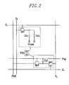
- FIG. 2is an equivalent circuit diagram of a pixel including a photo sensing circuit of an LCD according to an embodiment of the present invention
- FIG. 3is an equivalent circuit diagram of a pixel including a pressure sensing circuit of an LCD according to an embodiment of the present invention
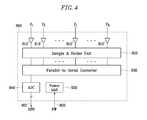
- FIG. 4is a block diagram of an integrated circuit (IC) including a sensing signal processor according to an embodiment of the present invention
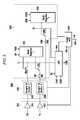
- FIG. 5is a schematic diagram of a sensing signal processor according to an embodiment of the present invention.
- FIG. 6is a block diagram of a complex IC chip including a sensing signal processor
- FIG. 7is a flow chart illustrating a method of driving an LCD according to an embodiment of the present invention.
- FIGS. 1 , 2 , 3 , 4 , and 5illustrate an embodiment of a touch detectable display device comprising an LCD 100 .
- FIG. 1is a block diagram of LCD 100 according to an embodiment of the present invention
- FIG. 2is an equivalent circuit diagram of a pixel including a photo sensing circuit of LCD 100 according to an embodiment of the present invention
- FIG. 3is an equivalent circuit diagram of a pixel including a pressure sensing circuit of LCD 100 according to an embodiment of the present invention.
- FIG. 4is a block diagram of an integrated circuit (IC) including a sensing signal processor according to an embodiment of the present invention
- FIG. 5is a schematic diagram of a sensing signal processor according to an embodiment of the present invention
- FIG. 6is a block diagram of a complex IC chip including a sensing signal processor.
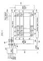
- an LCD 100includes a liquid crystal (LC) panel assembly 300 , an image scanning driver 400 , an image data driver 500 , a sensor scanning driver 700 , and a sensing signal processor 800 that are coupled with the panel assembly 300 , a gray voltage generator 550 coupled to the image data driver 500 , and a signal controller 600 controlling the above elements.
- LCliquid crystal
- the panel assembly 300includes a plurality of display signal lines G 1 -G n and D 1 -D m , a plurality of sensor signal lines S 1 -S N , P 1 -P M , Psg and Psd, and a plurality of pixels PX.
- the pixels PXare connected to the display signal lines G 1 -G n and D 1 -D m and the sensor signal lines S 1 -S N , P 1 -P M , Psg and Psd and arranged substantially in a matrix.
- the display signal linesinclude a plurality of image scanning lines G 1 -G n transmitting image scanning signals and a plurality of image data lines D 1 -D m transmitting image data signals.
- the sensor signal linesinclude a plurality of sensor scanning lines S 1 -S N transmitting sensor scanning signals, a plurality of sensor data lines P 1 -P M transmitting sensor data signals, a plurality of control voltage lines Psg transmitting a sensor control voltage, and a plurality of input voltage lines Psd transmitting a sensor input voltage.
- the image scanning lines G 1 -G n and the sensor scanning lines S 1 -S Nextend substantially in a row direction and substantially parallel to each other, while the image data lines D 1 -D m and the sensor data lines P 1 -P M extend substantially in a column direction and substantially parallel to each other.
- At least some of the pixelsfurther include at least one of a photo sensing circuit and a pressure sensing circuit.
- PX 1includes a photo sensing circuit SC 1 connected to sensor signal lines S i , P j , Psg and Psd
- PX 2includes a pressure sensing circuit SC 2 connected to sensor signal lines S i , P j and Psg.
- fewer than all of the pixels PXmay include the sensing circuits SC 1 or SC 2 .
- the concentration of the sensing circuits SC 1 and SC 2may be varied and thus the number N of the sensor scanning lines S 1 -S N and the number M of the sensor data lines P 1 -P M may be varied.
- the resolution of the LCDis equivalent to QVGA (quarter video graphics array) resolution (240 ⁇ 320 dots).
- QVGAquarter video graphics array
- one sensing circuitis assigned to every three pixels PX.
- QQVGAquarter QVGA
- one sensing circuitis assigned to every twelve pixels PX.
- one dotis a basic unit for representing a color, and includes a set of three pixels for color components; for example, red, green, and blue pixels.
- the sensing circuits SC 1 and/or SC 2may be separated from the pixels PX and may be provided between the pixels PX or in a separately prepared area.
- a photo sensing circuit SC 1 and a pressure sensing circuit SC 2may be connected to the same sensor data line P j , but it is preferable that the photo sensing circuit SC 1 and the pressure sensing circuit SC 2 are connected to different sensor data lines.
- the display circuit DCincludes a switching element Qs 1 connected to an image scanning line G i and an image data line D j , and a LC capacitor Clc and a storage capacitor Cst that are connected to the switching element Qs 1 .
- the storage capacitor Cstmay be omitted.
- the switching element Qs 1has three terminals, i.e., a control terminal connected to the image scanning line G i , an input terminal connected to the image data line D j , and an output terminal connected to the LC capacitor Clc and the storage capacitor Cst.
- the LC capacitor Clcincludes a pair of terminals and a liquid crystal layer (not shown) interposed therebetween and it is connected between the switching element Qs 1 and a common voltage Vcom.
- the two terminals of the LC capacitor Clcmay be disposed on two panels (not shown) of the panel assembly 300 .
- One of the two terminalsis often referred to as a pixel electrode, and the other of the two terminals is often referred to as a common electrode.
- the common electrodeoften covers an entire area of one of the two panels and is supplied with a common voltage Vcom.
- the pixel electrode and the common electrodemay be provided on the same panel, and in this case, at least one of the pixel electrode and the common electrode has a shape of bar or stripe.
- the storage capacitor Cstassists the LC capacitor Clc and is connected between the switching element Qs 1 and a predetermined voltage such as the common voltage Vcom.
- the storage capacitor Cstmay include the pixel electrode and a separate signal line, which is provided on one of the two panels and overlaps the pixel electrode via an insulator.
- the storage capacitor Cstincludes the pixel electrode and an adjacent image scanning line called a previous image scanning line, which overlaps the pixel electrode via an insulator.
- each pixel PXuniquely represents one of primary colors (i.e., spatial division) or each pixel PX sequentially represents the primary colors in turn (i.e., temporal division) such that a spatial or temporal sum of the primary colors is recognized as a desired color.
- An example of a set of the primary colorsincludes red, green, and blue colors.
- each pixel PXincludes a color filter representing one of the primary colors in an area facing the pixel electrode
- the photo sensing circuit SC 1 shown in FIG. 2includes a photo sensing element Qp 1 connected to a control voltage line Psg and an input voltage line Psd, a sensor capacitor Cp 1 connected to the photo sensing element Qp 1 , and a switching element Qs 2 connected to a sensor scanning line S i , the photo sensing element Qp 1 , and a sensor data line P j .
- the photo sensing element Qp 1has three terminals, i.e., a control terminal connected to the control voltage line Psg to be biased by the sensor control voltage, an input terminal connected to the input voltage line Psd to be biased by the sensor input voltage, and an output terminal connected to the switching element Qs 2 .
- the photo sensing element Qp 1includes a photoelectric material that generates a photocurrent upon receipt of light.
- An example of the photo sensing element Qp 1is a thin film transistor having an amorphous silicon or polysilicon channel that can generate a photocurrent.
- the sensor control voltage applied to the control terminal of the photo sensing element Qp 1is sufficiently low or sufficiently high to keep the photo sensing element Qp 1 in an off state without incident light.
- the sensor input voltage applied to the input terminal of the photo sensing element Qp 1is sufficiently high or sufficiently low to keep the photocurrent flowing in a direction.
- the sensor input voltageis sufficiently high or sufficiently low so that the photocurrent flows toward the switching element Qs 2 and flows into the sensor capacitor Cp 1 to charge the sensor capacitor Cp 1 .
- the sensor capacitor Cp 1is connected between the control terminal and the output terminal of the photo sensing element Qp 1 .
- the sensor capacitor Cp 1stores electrical charges output from the photo sensing element Qp 1 to substantially maintain a predetermined voltage.
- the sensor capacitor Cp 1may be omitted.
- the switching element Qs 2also has three terminals, i.e., a control terminal connected to the sensor scanning line S i , an input terminal connected to the output terminal of the photo sensing element Qp 1 , and an output terminal connected to the sensor data line P j .
- the switching element Qs 2outputs a sensor output signal to the sensor data line P j in response to the sensor scanning signal from the sensor scanning line S i .
- the sensor output signalis a sensing current from the photo sensing element Qp 1 .
- the sensor output signalmay be a voltage stored in the sensor capacitor Cp 1 .
- the pressure sensing circuit SC 2 shown in FIG. 3includes a pressure sensing element PU 1 connected to the common voltage Vcom and a control voltage line Psg, and a switching element Qs 3 connected to a sensor scanning line S i , the pressure sensing element PU 1 , and a sensor data line P j .
- the pressure sensing element PU 1includes a pressure switch SW 1 connected to the common voltage Vcom and a driving transistor Qp 2 connected between the switch SW 1 and the switching element Qs 3 .
- the pressure switch SW 1connects the driving transistor Qp 2 to the common voltage Vcom under a pressure initiated by a touch exerted on the panel assembly 300 .
- the pressuremay make an electrode (not shown) supplied with the common voltage Vcom approach a terminal of the driving transistor Qp 2 to be in contact therewith.
- the switch SW 1may use another physical quantity for connecting the driving transistor Qp 2 to the common voltage Vcom and in this case, the pressure sensing element PU 1 and the pressure switch SW 1 may be referred to using names indicative of the physical quantity.
- the driving transistor Qp 2has three terminals, i.e., a control terminal connected to the control voltage line Psg to be biased by the sensor control voltage, an input terminal connected to the switch SW 1 , and an output terminal connected to the switching element Qs 3 .
- the driving transistor Qp 2generates and outputs an electrical current upon receipt of the common voltage Vcom from the switch SW 1 .
- the switching element Qs 3also has three terminals, i.e., a control terminal connected to the sensor scanning line S i , an input terminal connected to the output terminal of the driving transistor Qp 2 , and an output terminal connected to the sensor data line P j .
- the switching element Qs 3outputs the current from the driving transistor Qp 2 to the sensor data line P j as a sensor output signal in response to the sensor scanning signal from the sensor scanning line S i .
- the switching elements Qs 1 , Qs 2 and Qs 3 , the photo sensing element Qp 1 , and the driving transistor Qp 2may include amorphous silicon or polysilicon thin film transistors (TFTs).
- the pressure sensing circuit SC 2can correctly identify the existence of a touch, but it may not identify the precise position of the touch since the pressure following the touch may cover a wide area.
- the photo sensing circuit SC 1can identify the precise position of a touch of an object by sensing the variation of light illuminance caused by a shadow of the object, while it may not correctly identify the existence of the touch since the variation of illuminance can be generated by various causes other than a touch.
- the illuminancemay vary due to the presence of an object disposed near the panel assembly 300 that does not touch the panel assembly 300 .
- the resolution of the sensing circuitsmay be made as small as practical.
- the resolution of the pressure sensing circuitsis preferably smaller than the resolution of the photo sensing circuits, since the determination of the existence of a touch can be appropriately performed under a low resolution of the pressure sensing circuits. That is, the system may be configured so that the resolution of the sensing circuits is high enough to reliably and accurately determine a user input based on detection of a touch at a touch position.
- the resolutionneed not be as high as the LCD resolution, which is selected to provide a desired image quality.
- One or more polarizersare provided at the panel assembly 300 .
- the gray voltage generator 550generates two sets of gray voltages related to a transmittance of the pixels.
- the gray voltages in a first sethave a positive polarity with respect to the common voltage Vcom, while the gray voltages in a second set have a negative polarity with respect to the common voltage Vcom.
- the image scanning driver 400is connected to the image scanning lines G 1 -G n of the panel assembly 300 and synthesizes a gate-on voltage and a gate-off voltage to generate the image scanning signals for application to the image scanning lines G 1 -G n .
- the image data driver 500is connected to the image data lines D 1 -D m of the panel assembly 300 and applies image data signals selected from the gray voltages to the image data lines D 1 -D m .
- the sensor scanning driver 700is connected to the sensor scanning lines S 1 -S N of the panel assembly 300 and synthesizes a gate-on voltage and a gate-off voltage to generate the sensor scanning signals for application to the sensor scanning lines S 1 -S N .
- the sensing signal processor 800is connected to the sensor data lines P 1 -P M of the display panel 300 and receives and analog-to-digital converts the sensor data signals from the sensor data lines P 1 -P M to generate digital sensor data signals DSN.
- the sensor data signals carried by the sensor data lines P 1 -P Mmay be current signals and in this case, the sensing signal processor 800 converts the current signals into voltage signals before the analog-to-digital conversion.
- One sensor data signal carried by one sensor data line P 1 -P M at a timemay include one sensor output signal from one switching elements Qs 2 or may include at least two sensor output signals outputted from at least two switching elements Qs 2 .
- the signal controller 600controls the image scanning driver 400 , the image data driver 500 , the sensor scanning driver 700 , and the sensing signal processor 800 , etc.
- Each of the processing units 400 , 500 , 600 , 700 and 800may include at least one integrated circuit (IC) chip mounted on the LC panel assembly 300 or on a flexible printed circuit (FPC) film in a tape carrier package (TCP), which may be attached to the panel assembly 300 .
- ICintegrated circuit
- FPCflexible printed circuit
- TCPtape carrier package
- at least one (and/or a portion thereof) of the processing units 400 , 500 , 600 , 700 and 800may be integrated into the panel assembly 300 along with the signal lines G 1 -G n , D 1 -D m , S 1 -S N , P 1 -P M , Psg and Psd, the switching elements Qs 1 , Qs 2 and Qs 3 , and the photo sensing elements Qp 1 .
- all the processing units 400 , 500 , 600 , 700 and 800may be integrated into a single IC chip, but at least one of the processing units 400 , 500 , 600 , 700 and 800 or at least one circuit element in at least one of the processing units 400 , 500 , 600 , 700 and 800 may be disposed out of the single IC chip.
- the LCDmay further include a touch determination unit (not shown) receiving the digital sensor data signals DSN from the sensing signal processor 800 on a bus 801 and determining whether and where a touch exists.
- the touch determination unitmay be included in the signal controller 600 or may be implemented differently (for example, as an independent IC chip).
- a sensing signal processor 800may be implemented as a single IC chip including a plurality of amplifiers 810 , a sample and holder unit 820 , a parallel-to-serial converter 830 , an analog-to-digital converter 840 , and a power unit 850 .
- the amplifiers 810 , the sample and holder unit 820 , the parallel-to-serial converter 830 , and an analog-to-digital converter 840are connected in series.
- the amplifiers 810includes a predetermined number x of first amplifiers 811 and another predetermined number y of second amplifiers 812 .
- the first amplifiers 811are connected to first sensor data lines P 1 -P M connected to the photo sensing circuits SC 1 and receive, amplify, and filter photo sensor data signals Vp from the first sensor data lines P 1 -P M .
- the second amplifiers 812are connected to second sensor data lines P 1 -P M connected to the pressure sensing circuits SC 2 , and receive, amplify, and filter pressure sensor data signals Vt from the second sensor data lines P 1 -P M .
- the number xcorresponds to horizontal resolution of the photo sensing circuits SC 1
- the sample and holder unit 820includes a first sample and holder 821 and a second sample and holder 822 .
- the first/second sample and holder 821 / 822is coupled with the first/second amplifiers 811 / 812 and sample-and-holds the amplified photo/pressure sensor data signals Vp/Vt.
- the parallel-to-serial converter 830includes first switching transistors TR 1 , second switching transistors TR 2 , first switches SW 1 , second switches SW 2 , a first shift register 831 , and a second shift register 832 .
- the parallel-to-serial converter 830converts the processed sensor data signals Vp and Vt from the sample and holder unit 820 into serial signals.
- Each of the first switching transistors TR 1has three terminals, i.e., an input terminal connected to the first or the second sample and holder 821 or 822 , an output terminal connected to a signal line L 1 , and a control terminal connected to the first shift register 831 .
- the first switching transistors TR 1output the processed sensor data signals Vp and Vt to the analog-to-digital converter 840 in synchronization with clock pulses from the first shift register 831 .
- Each of the second switching transistors TR 2has three terminals, i.e., an input terminal connected to the second sample and holder 822 , an output terminal connected to a signal line L 2 , and a control terminal connected to the second shift register 832 .
- the second switching transistors TR 2output the processed pressure sensor data signals Vt to the analog-to-digital converter 840 in synchronization with clock pulses from the second shift register 832 .
- the first shift register 831operates in response to a selection signal SDB and outputs clock pulses to the first switching transistors TR 1 in synchronization with a first clock signal CLK 1 .
- the processed sensor data signals Vp and Vtare serially inputted into the analog-to-digital converter 840 through the first switching transistors TR 1 that turn on in sequence.
- the second shift register 832operates in response to an inversion signal SDB having a voltage waveform inverted from the selection signal SD outputs clock pulses to the second switching transistors TR 2 in synchronization with a second clock signal CLK 2 .
- the processed pressure sensor data signals Vtare serially inputted into the analog-to-digital converter 840 through the second switching transistors TR 2 that turn on in sequence.
- the frequency f 2 of the second clock signal CLK 2is lower than the frequency f 1 of the first clock signal CLK 1 .
- f 13 ⁇ f 2 .
- the first switch SW 1is connected between the second sample and holder 822 and the first switching transistor TR 1 , and transmits the pressure sensor data signal Vt to the first switching transistor TR 1 in response to the selection signal SD.
- the second switch SW 2is connected between the second sample and holder 822 and the second switching transistor TR 2 , and transmits the pressure sensor data signal Vt to the second switching transistor TR 2 in response to the inversion signal SDB.
- the second shift register 832 and the second switch SW 2may include an inverter (not shown) such that they operates in response to the selection signal SD instead of the inversion signal SDB.
- the first switch SW 1 and the second switch SW 2may form a single switch, which transmits the pressure sensor data signal Vt to one of the first and the second switching transistors TR 1 and TR 2 in response to the selection signal SD.
- the analog-to-digital converter 840receives signals from the first signal line L 1 and the second signal line L 2 in response to the selection signal SD.
- the analog-to-digital converter 840also selects one of the first clock signal CLK 1 and the second clock signal CLK 2 in response to the selection signal SD and operates in synchronization with the selected clock signal CLK 1 or CLK 2 .
- the analog-to-digital converter 840converts the sensor data signals Vp and Vt inputted through the first signal line L 1 into the digital sensor data signals DSN in synchronization with the first clock signal CLK 1 , or converts the pressure sensor data signals Vp inputted through the second signal line L 2 into the digital sensor data signals DSN in synchronization with the second clock signal CLK 2 .
- the analog-to-digital converter 840includes a multiplexer (not shown) for selecting one of the first and the second clock signals CLK 1 and CLK 2 and for selecting one of the first and the second signal lines L 1 and L 2 .
- the power unit 850is supplied with power PW on a line 802 from an external source and provides the power for the driving blocks 810 - 840 , the amplifiers 811 , and blocks the power supplied to the first sample and holder 821 and the first shift register 831 , or the power supplied to the second shift register 832 in response to the selection signal SD.
- the image data driver 500 , the sensing signal processor 800 , and the signal controller 600are integrated into a complex IC 1000 as shown in FIG. 6 .
- the complex IC 1000may be implemented as a single chip as shown in FIG. 5 .
- a complex IC 1000 shown in FIG. 6includes a gray voltage generator 550 , an image data driver 500 , a plurality of output buffers 510 , an interface 610 , a signal controller 600 , a sensing signal processor 800 , and a power unit 900 .
- the sensing signal processor 800includes amplifiers 810 , a sample and holding unit 820 , a parallel-to-serial converter 830 , and an analog-to-digital converter 840 .
- the above-described touch determination unitmay be also integrated into the complex IC 1000 .
- the gray voltage generator 550 , the image data driver 500 , and the signal controller 600have substantially the same function as described above and the detailed description thereof will be omitted.
- the output buffers 510are connected to data lines D 1 -D m , and are configured to output image data voltages from the image data driver 500 to the data lines D 1 -D m .
- the number of the output buffers 510is determined by the numbers of the data lines D 1 -D m , while the number of the amplifiers 810 is determined by the number of the sensor data lines P 1 -P M .
- the number of the output buffers 510is three times the number of the amplifiers 810 .
- output terminals of the complex IC 1000 coupled to the output buffers 510 and input terminals of the complex IC 1000 coupled to the amplifiers 810are alternately arranged in a manner that one input terminal is provided for every three output terminals.
- the resolution of the LCDis equivalent to QVGA
- the resolution of the sensing circuits C 1 and C 2is equivalent to QQVGA
- one input terminalis provided for every six output terminals.
- the arrangement of the output terminals and the input terminals of the complex IC 1000 in association with the output buffers 510 and the amplifiers 810may be varied according to the arrangement of the sensing circuits C 1 and C 2 .
- the interface 610receives input image signals R, G and B on a bus 605 and input control signals CNT on a bus 606 from an external device and converts the received signals R, G and B and CNT to be processible by the signal controller 600 , etc.
- the power unit 900receives power PW on a power line 802 from an external source and supplies the power PW to driving blocks in the complex IC 1000 .
- the power unitblocks the power supplied to the first amplifiers 811 , the first sample and holder 821 , and the first shift register 831 , or the power supplied to the second shift register 832 .
- the integration of the units 500 , 600 , 800 and 900 into the complex IC 1000may decrease the size of the panel assembly 300 , the power consumption, and the manufacturing cost.
- At least one of the processing units 500 , 600 , 800 and 900 or at least one circuit element in at least one of the processing units 500 , 600 , 800 and 900may be disposed out of the single IC chip.
- the image scanning driver 400 or the sensor scanning driver 700may be also incorporated into the complex IC 1000 .
- the complex IC 1000may further include latches, registers, memories, and/or other additional elements for display operation and sensing operation.
- FIGS. 1-6the operation of the above-described LCD will be described in detail, referring to FIGS. 1-6 .
- the signal controller 600is supplied with input image signals R, G and B on bus 605 and input control signals CNT on bus 606 for controlling the display thereof from an external graphics controller (not shown).
- the input control signals CNTinclude a vertical synchronization signal Vsync, a horizontal synchronization signal Hsync, a main clock MCLK, and a data enable signal DE.
- the signal controller 600On the basis of the input control signals CNT and the input image signals R, G and B, the signal controller 600 generates image scanning control signals CONT 1 , image data control signals CONT 2 , sensor scanning control signals CONT 3 , and sensor data control signals CONT 4 , and it processes the image signals R, G and B to be used for the operation of the display panel 300 .
- the signal controller 600sends the scanning control signals CONT 1 to the image scanning driver 400 on bus 615 , the processed image signals DAT and the data control signals CONT 2 to the image data driver 500 on bus 614 and 613 , respectively, the sensor scanning control signals CONT 3 to the sensor scanning driver 700 on bus 612 , and the sensor data control signals CONT 4 to the sensing signal processor 800 on bus 616 .
- the image scanning control signals CONT 1include an image scanning start signal STV for signaling a start of image scanning and at least one clock signal for controlling the output time of the gate-on voltage.
- the image scanning control signals CONT 1may include an output enable signal OE for defining the duration of the gate-on voltage.
- the image data control signals CONT 2include a horizontal synchronization start signal STH for signaling the start of image data transmission for a group of pixels PX, a load signal LOAD for initiating the application of the image data signals to the image data lines D 1 -D m , and a data clock signal HCLK.
- the image data control signal CONT 2may further include an inversion signal RVS for reversing the polarity of the image data signals (with respect to the common voltage Vcom).
- the image data driver 500Responsive to the image data control signals CONT 2 from the signal controller 600 , the image data driver 500 receives a packet of the digital image signals DAT for the group of pixels PX from the signal controller 600 , converts the digital image signals DAT into analog image data signals, and applies the analog image data signals to the image data lines D 1 -D m .
- the image scanning driver 400applies the gate-on voltage to an image scanning line G 1 -G n in response to the image scanning control signals CONT 1 from the signal controller 600 , thereby turning on the switching transistors Qs 1 connected thereto.
- the image data signals applied to the image data lines D 1 -D mare then supplied to the display circuit DC of the pixels PX through the activated switching transistors Qs 1 .
- the difference between the voltage of an image data signal and the common voltage Vcomis represented as a voltage across the LC capacitor Clc, which is referred to as a pixel voltage.
- the LC molecules in the LC capacitor Clchave orientations depending on the magnitude of the pixel voltage, and the molecular orientations determine the polarization of light passing through the LC layer 3 .
- the polarizer(s)converts the light polarization into the light transmittance to display images.
- all image scanning lines G 1 -G nare sequentially supplied with the gate-on voltage, thereby applying the image data signals to all pixels PX to display an image for a frame.
- the inversion control signal RVS applied to the image data driver 500is controlled such that the polarity of the image data signals is reversed (which is referred to as “frame inversion”).
- the inversion control signal RVSmay be also controlled such that the polarity of the image data signals flowing in a data line are periodically reversed during one frame (for example, row inversion and dot inversion), or the polarity of the image data signals in one packet are reversed (for example, column inversion and dot inversion).
- the sensor scanning control signals CONT 3include a sensor scanning start signal for signaling a start of sensor scanning and at least one clock signal for controlling the output time of the gate-on voltage onto the sensor scanning lines S 1 -S N .
- the sensor data control signals CONT 4includes a selection signal SD, an inversion signal SDB, and clock signals CLK 1 and CLK 2 (as shown in FIG. 5 ).
- the sensor scanning driver 700applies the gate-on voltage to the sensor scanning lines S 1 -S N to turn on the switching elements Qs 2 and Qs 3 connected thereto in response to the sensing control signals CONT 3 . Then, the switching elements Qs 2 and Qs 3 output sensor output signals to the sensor data lines P 1 -P M to form sensor data signals Vp and Vt, and the sensor data signals Vp and Vt are input into the sensing signal processor 800 .
- the sensor data signals Vp and Vtare amplified and filtered to have suitable levels by the amplifiers 810 and sampled-and-held by the sample and holding unit 820 .
- the sampled-and-held sensor data signalsare converted into serial signals by the parallel-to-serial converter 830 , and the parallel analog sensor data signals are then converted into digital sensor data signals DSN by the analog-to-digital converter 840 to be sent to a touch determination unit.
- the touch determination unitappropriately processes the digital sensor data signals DSN to determine touch information indicative of the detection of a touch and the position of the detected touch.
- the touch determination unitoutputs touch information to an external device.
- the external devicesend image signals generated based on information about the touch to the LCD.
- FIG. 7is a flow chart illustrating a method of driving an LCD according to an embodiment of the present invention.
- the LCD according to an embodiment of the present inventionperforms a sensing operation in two modes, i.e., in a normal mode NM or a power saving mode FS.
- the selection of the normal mode NM or the power saving mode PSmay be determined by the selection signal SD and/or the inversion signal SDB.
- the LCDstarts its operation in the power saving mode PS ( 10 ).
- the switch SW 1is turned off, while the switch SW 2 is turned on.
- the first shift register 831is disabled, while the second shift register 832 is enabled.
- the first shift register 831 , the first amplifiers 811 , and the first sample and holder 821are blocked from the power PW, while the second shift register 832 is supplied with the power PW.
- the second shift register 832 and the analog-to-digital converter 840operate according to the second clock signal CLK 2 .
- the power saving mode PSonly the pressure sensor data signals Vt are processed to be converted into the digital sensor data signals DSN, thereby determining whether a touch exists.
- the first amplifiers 811 , the first sample and holder 821 , and the first shift register 831are not supplied with the power PW, reducing power consumption.
- the second shift register 832 and the analog-to-digital converter 840operate in synchronization with the second clock signal CLK 2 having relatively low frequency to further reduce the power consumption.
- a frame counter FCis initialized into zero ( 20 ).
- the frame counter FCis a variable for counting the number of frames.
- the frame counter FCis used to initiate a change from the normal mode NM into the power saving mode PS.
- the systemdetermines whether a touch is detected during the power saving mode PS ( 30 ).
- the LCDmaintains the power saving mode PS ( 10 ) and continues to determine whether a touch is detected. When it is determined that a touch is detected, the LCD converts the operation mode into the normal mode NM ( 40 ).
- the switch SW 1is turned on, while the switch SW 2 is turned off.
- the first shift register 831is enabled, while the second shift register 832 is disabled.
- the first shift register 831is powered, while the second shift register 832 is cut off from the power.
- the first shift register 831 and the analog-to-digital converter 840operate according to the first clock signal CLK 1 .
- the sensor data signals Vp and Vtare processed to be converted into the digital sensor data signals DSN to determine detection of a touch and its position. The system determines whether a touch is detected during the normal mode NM ( 50 ).
- the frame counter FCis initialized into zero ( 60 ), the normal mode NM is maintained ( 40 ), and the system continues to determine whether a touch is detected and, if so, its associated position.
- the frame counter FCis increased by one ( 70 ).
- a value of the frame counter FCis compared with a predetermined value N ( 80 ).
- the normal mode NMis maintained ( 40 ).
- the value of the frame counter FCis equal to the predetermined value N, the operation mode is converted into the power saving mode PS ( 10 ).
- the predetermined value Nis a natural number.
- the operation modewhen a touch is detected during the power saving mode PS, the operation mode is converted into the normal mode NM, and when there is no touch for a predetermined time during the normal mode NM, the operation mode is converted into the power saving mode PS again.
- the LCDoperates in the power saving mode PS when there is no touch to reduce the power consumption.
- This embodimentmay be particularly beneficial for portable devices employing LCDs, such as laptop computers, PDAs, cell phones, and other portable devices.
- the present inventioncan be also employed in other flat panel displays such as an organic light emitting diode (OLED) display and a plasma display panel (PDP).
- OLEDorganic light emitting diode
- PDPplasma display panel
Landscapes
- Engineering & Computer Science (AREA)
- Theoretical Computer Science (AREA)
- General Engineering & Computer Science (AREA)
- Physics & Mathematics (AREA)
- General Physics & Mathematics (AREA)
- Human Computer Interaction (AREA)
- Computer Hardware Design (AREA)
- Computing Systems (AREA)
- Chemical & Material Sciences (AREA)
- Crystallography & Structural Chemistry (AREA)
- Control Of Indicators Other Than Cathode Ray Tubes (AREA)
- Liquid Crystal (AREA)
- Position Input By Displaying (AREA)
- Liquid Crystal Display Device Control (AREA)
- Electronic Switches (AREA)
- Measuring Fluid Pressure (AREA)
Abstract
Description
Claims (39)
Applications Claiming Priority (2)
| Application Number | Priority Date | Filing Date | Title |
|---|---|---|---|
| KR1020040111073AKR101160828B1 (en) | 2004-12-23 | 2004-12-23 | Display device, driving method thereof, and driving apparatus for display device |
| KR10-2004-0111073 | 2004-12-23 |
Publications (2)
| Publication Number | Publication Date |
|---|---|
| US20060138983A1 US20060138983A1 (en) | 2006-06-29 |
| US7973777B2true US7973777B2 (en) | 2011-07-05 |
Family
ID=36610674
Family Applications (1)
| Application Number | Title | Priority Date | Filing Date |
|---|---|---|---|
| US11/315,088Active2028-09-14US7973777B2 (en) | 2004-12-23 | 2005-12-21 | Display device and driving apparatus including a photo sensing circuit and a pressure sensing circuit and method thereof |
Country Status (5)
| Country | Link |
|---|---|
| US (1) | US7973777B2 (en) |
| JP (1) | JP4908844B2 (en) |
| KR (1) | KR101160828B1 (en) |
| CN (4) | CN101398731B (en) |
| TW (1) | TWI401641B (en) |
Cited By (7)
| Publication number | Priority date | Publication date | Assignee | Title |
|---|---|---|---|---|
| US20090251425A1 (en)* | 2008-04-08 | 2009-10-08 | Lg Display Co., Ltd. | Multi-touch system and driving method thereof |
| US20100097340A1 (en)* | 2008-10-20 | 2010-04-22 | Sony Corporation | Liquid-crystal display panel and chopper-type comparator |
| US20100231390A1 (en)* | 2009-03-13 | 2010-09-16 | Canon Kabushiki Kaisha | Image processing apparatus |
| US20110115724A1 (en)* | 2009-11-16 | 2011-05-19 | Jee-Hoon Jeon | Display apparatus |
| US20120032801A1 (en)* | 2009-04-24 | 2012-02-09 | Kyocera Corporation | Input apparatus and input method |
| US9417754B2 (en) | 2011-08-05 | 2016-08-16 | P4tents1, LLC | User interface system, method, and computer program product |
| US10797725B2 (en)* | 2018-12-17 | 2020-10-06 | SK Hynix Inc. | Parallel-to-serial conversion circuit |
Families Citing this family (52)
| Publication number | Priority date | Publication date | Assignee | Title |
|---|---|---|---|---|
| US9064772B2 (en)* | 2005-10-07 | 2015-06-23 | Integrated Digital Technologies, Inc. | Touch screen system having dual touch sensing function |
| WO2008047677A1 (en)* | 2006-10-19 | 2008-04-24 | Sharp Kabushiki Kaisha | Display apparatus |
| CN101561601B (en)* | 2008-04-14 | 2012-05-30 | 北京京东方光电科技有限公司 | Method and device for driving liquid crystal display |
| JP5399799B2 (en)* | 2008-07-17 | 2014-01-29 | 三星ディスプレイ株式會社 | Display device |
| JP5252427B2 (en)* | 2008-10-01 | 2013-07-31 | 株式会社ジャパンディスプレイウェスト | Input device and display device |
| KR101337042B1 (en)* | 2008-10-21 | 2013-12-05 | 엘지디스플레이 주식회사 | Touch panel display device and driving method thereof |
| JP2010151920A (en)* | 2008-12-24 | 2010-07-08 | Seiko Epson Corp | Image processing apparatus, projection display device, and method for reducing power consumption of image processing apparatus |
| KR101578075B1 (en) | 2009-04-20 | 2015-12-17 | 삼성디스플레이 주식회사 | Touch detection method and touch detection device for performing the same |
| KR101059079B1 (en)* | 2009-06-12 | 2011-08-24 | 주식회사 켐트로닉스 | Method for reducing power consumption of a device of touch sensing and the device |
| US8576183B2 (en)* | 2009-09-23 | 2013-11-05 | Infineon Technologies Ag | Devices and methods for controlling both LED and touch sense elements via a single IC package pin |
| EP2315102B1 (en) | 2009-10-02 | 2018-01-31 | BlackBerry Limited | A low power wakeup detection circuit and a portable electronic device having a low power wakeup detection circuit |
| US8970507B2 (en)* | 2009-10-02 | 2015-03-03 | Blackberry Limited | Method of waking up and a portable electronic device configured to perform the same |
| US8780055B2 (en)* | 2009-10-02 | 2014-07-15 | Blackberry Limited | Low power wakeup detection circuit and a portable electronic device having a low power wakeup detection circuit |
| EP2315101B1 (en)* | 2009-10-02 | 2014-01-29 | BlackBerry Limited | A method of waking up and a portable electronic device configured to perform the same |
| TWI397736B (en)* | 2009-10-13 | 2013-06-01 | Au Optronics Corp | Active device arry substrate and display device |
| JP5232924B2 (en)* | 2009-12-25 | 2013-07-10 | シャープ株式会社 | Display device and display device control method |
| BR112012016739A2 (en)* | 2010-01-08 | 2017-06-13 | Sharp Kabushiki Kaisaha | "display device with optical sensors" |
| TWI500313B (en)* | 2010-06-04 | 2015-09-11 | Au Optronics Corp | Image scanning system and method of controlling the same |
| KR101351418B1 (en)* | 2010-10-26 | 2014-01-15 | 엘지디스플레이 주식회사 | Display device using infrared sensor module and method the same |
| US9262002B2 (en)* | 2010-11-03 | 2016-02-16 | Qualcomm Incorporated | Force sensing touch screen |
| CN101996684B (en)* | 2010-11-10 | 2013-07-24 | 友达光电股份有限公司 | Shift register and touch device |
| WO2012079187A1 (en)* | 2010-12-13 | 2012-06-21 | Telefonaktiebolaget L M Ericsson (Publ) | A base station subsystem, a rbs part and a tma part and methods thereof for synchronizing the rbs part and the tma part |
| US8988384B2 (en)* | 2011-09-23 | 2015-03-24 | Apple Inc. | Force sensor interface for touch controller |
| US20130100044A1 (en)* | 2011-10-24 | 2013-04-25 | Motorola Mobility, Inc. | Method for Detecting Wake Conditions of a Portable Electronic Device |
| US9246486B2 (en) | 2011-12-16 | 2016-01-26 | Apple Inc. | Electronic device with noise-cancelling force sensor |
| CN103296947A (en)* | 2012-02-28 | 2013-09-11 | 快捷半导体(苏州)有限公司 | Motor driving circuit, motor driving method and application equipment of motor driving method |
| FR2987929B1 (en) | 2012-03-09 | 2014-04-11 | Digital Art Internat | DEVICE FOR SURFACE DIFFUSION OF LUMINOUS IMAGES AT THE SCALE OF THE HUMAN BODY |
| US20130265256A1 (en)* | 2012-04-07 | 2013-10-10 | Cambridge Touch Technologies, Ltd. | Pressure sensing display device |
| CN102722290B (en)* | 2012-05-30 | 2016-06-22 | 深圳Tcl新技术有限公司 | The anti-tampering processing method of touch screen, device and touch screen terminal |
| CN103218076B (en)* | 2013-03-29 | 2017-02-08 | 合肥京东方光电科技有限公司 | Embedded type touch screen and display device |
| KR102313098B1 (en) | 2014-02-18 | 2021-10-14 | 케임브리지 터치 테크놀로지스 리미티드 | Dynamic switching of power modes for touch screens using force touch |
| CN104200784B (en) | 2014-07-24 | 2017-07-28 | 京东方科技集团股份有限公司 | Pixel-driving circuit and its driving method, array base palte, Transflective display device |
| EP3457263A1 (en) | 2014-12-23 | 2019-03-20 | Cambridge Touch Technologies, Ltd. | Pressure-sensitive touch panel |
| GB2533667B (en) | 2014-12-23 | 2017-07-19 | Cambridge Touch Tech Ltd | Pressure-sensitive touch panel |
| KR102268521B1 (en)* | 2014-12-24 | 2021-06-24 | 엘지디스플레이 주식회사 | Display device and method for driving the same |
| KR102273499B1 (en)* | 2014-12-29 | 2021-07-07 | 엘지디스플레이 주식회사 | Display device having a touch sensor and driving method thereof |
| CN104679355B (en)* | 2015-03-19 | 2017-10-10 | 合肥鑫晟光电科技有限公司 | A kind of optical touch screen and display device |
| US10386952B2 (en) | 2015-07-09 | 2019-08-20 | Shenzhen New Degree Technology Co., Ltd. | Force sensing touch system including a strain amplifying structure and computing device with a force sensing touch system |
| GB2544307B (en) | 2015-11-12 | 2018-02-07 | Cambridge Touch Tech Ltd | Processing signals from a touchscreen panel |
| US20170168615A1 (en)* | 2015-12-15 | 2017-06-15 | Novatek Microelectronics Corp. | Display device and control device thereof |
| GB2544353B (en) | 2015-12-23 | 2018-02-21 | Cambridge Touch Tech Ltd | Pressure-sensitive touch panel |
| US10282046B2 (en) | 2015-12-23 | 2019-05-07 | Cambridge Touch Technologies Ltd. | Pressure-sensitive touch panel |
| GB2547031B (en) | 2016-02-05 | 2019-09-25 | Cambridge Touch Tech Ltd | Touchscreen panel signal processing |
| CN106406496A (en)* | 2016-09-05 | 2017-02-15 | 芯海科技(深圳)股份有限公司 | Low power consumption control method for pressure-sensitive key identification device |
| CN107102779B (en)* | 2017-06-06 | 2020-02-07 | 上海天马微电子有限公司 | Display panel, control method thereof and display device |
| CN107219957B (en)* | 2017-06-20 | 2020-08-18 | 厦门天马微电子有限公司 | Array substrate and display panel |
| US11093088B2 (en) | 2017-08-08 | 2021-08-17 | Cambridge Touch Technologies Ltd. | Device for processing signals from a pressure-sensing touch panel |
| GB2565305A (en) | 2017-08-08 | 2019-02-13 | Cambridge Touch Tech Ltd | Device for processing signals from a pressure-sensing touch panel |
| KR102720150B1 (en)* | 2019-05-08 | 2024-10-22 | 삼성전자주식회사 | Data driver and display driving circuit comprising thereof |
| CN113632160B (en) | 2019-07-01 | 2023-06-20 | 斯纳普公司 | Systems and methods for low power common electrode voltage generation for displays |
| EP4141856A4 (en)* | 2020-04-24 | 2024-05-01 | Kyocera Corporation | Dot matrix display device and timing apparatus |
| TWI736332B (en)* | 2020-06-23 | 2021-08-11 | 友達光電股份有限公司 | Pixel circuit for touch sensing and optical sensing |
Citations (25)
| Publication number | Priority date | Publication date | Assignee | Title |
|---|---|---|---|---|
| US5159323A (en) | 1987-02-19 | 1992-10-27 | Semiconductor Energy Laboratory Co., Ltd. | Liquid crystal display |
| US5184018A (en)* | 1990-01-27 | 1993-02-02 | U.S. Philips Corporation | Sensor matrix |
| JPH0573201A (en) | 1991-09-11 | 1993-03-26 | Toshiba Corp | Coordinate detecting device |
| JPH0667793A (en) | 1992-08-19 | 1994-03-11 | Canon Inc | Coordinate input device |
| US5418551A (en) | 1988-12-19 | 1995-05-23 | Sharp Kabushiki Kaisha | Tablet integrated with display |
| JPH07302168A (en) | 1994-05-10 | 1995-11-14 | Casio Comput Co Ltd | Touch panel input device |
| US5479208A (en)* | 1993-03-25 | 1995-12-26 | Nec Corporation | Image sensors and driving method thereof |
| JPH08249121A (en) | 1995-03-15 | 1996-09-27 | Toshiba Corp | Coordinate input device |
| KR970008515A (en) | 1995-07-03 | 1997-02-24 | 김광호 | Roller of preheater for uniformly irradiating high frequency |
| JPH1039987A (en) | 1996-07-22 | 1998-02-13 | Tokyo Cosmos Electric Co Ltd | Touch panel |
| CN1179554A (en) | 1996-09-24 | 1998-04-22 | 三星电管株式会社 | Liquid crystal display device |
| JP2000075966A (en) | 1998-09-03 | 2000-03-14 | Canon Inc | Information processing device |
| US6195753B1 (en)* | 1997-06-09 | 2001-02-27 | Nec Corporation | Information processing apparatus with reduced power consumption |
| JP2001306255A (en) | 2000-04-27 | 2001-11-02 | Mitsumi Electric Co Ltd | Touch panel sensor |
| US6317840B1 (en)* | 1999-03-24 | 2001-11-13 | International Business Machines Corporation | Control of multiple equivalent functional units for power reduction |
| JP2002006686A (en) | 2000-06-20 | 2002-01-11 | Canon Inc | Information processing device |
| US6426736B1 (en) | 1998-12-28 | 2002-07-30 | Nec Corporation | Portable telephone with liquid crystal display |
| KR100347440B1 (en) | 2001-08-10 | 2002-08-03 | 주식회사 에이터치 | Method of transmiting axis data in the touch screen |
| US6445383B1 (en)* | 1998-02-09 | 2002-09-03 | Koninklijke Philips Electronics N.V. | System to detect a power management system resume event from a stylus and touch screen |
| US20020175887A1 (en)* | 1998-02-09 | 2002-11-28 | Suguru Yamazaki | Electrooptical apparatus and driving method therefor, liquid crystal display apparatus and driving method therefor, electrooptical apparatus and driving circuit therefor, and electronic equipment |
| US6504530B1 (en)* | 1999-09-07 | 2003-01-07 | Elo Touchsystems, Inc. | Touch confirming touchscreen utilizing plural touch sensors |
| JP2003167677A (en) | 2001-12-03 | 2003-06-13 | Sharp Corp | Touch panel input device and touch panel integrated display device |
| KR20030055857A (en) | 2001-12-27 | 2003-07-04 | 엘지.필립스 엘시디 주식회사 | Apparatus And Method for Driving Touch Panel |
| US6611921B2 (en)* | 2001-09-07 | 2003-08-26 | Microsoft Corporation | Input device with two input signal generating means having a power state where one input means is powered down and the other input means is cycled between a powered up state and a powered down state |
| US20060119590A1 (en)* | 2004-11-22 | 2006-06-08 | Jong-Woung Park | Touch sensible display device and driving method thereof |
Family Cites Families (19)
| Publication number | Priority date | Publication date | Assignee | Title |
|---|---|---|---|---|
| JPS63276085A (en)* | 1987-05-08 | 1988-11-14 | 株式会社東芝 | Compound display and input device |
| JPH0320817A (en)* | 1989-06-19 | 1991-01-29 | Nippon Telegr & Teleph Corp <Ntt> | Input/display unified type display device |
| GB9027481D0 (en)* | 1990-12-19 | 1991-02-06 | Philips Electronic Associated | Matrix display device with write-in facility |
| JPH05328039A (en)* | 1992-05-25 | 1993-12-10 | Ricoh Co Ltd | Image reader |
| GB9220104D0 (en)* | 1992-09-07 | 1992-11-04 | Philips Electronics Uk Ltd | Matrix display device with light sensing function |
| US5847690A (en)* | 1995-10-24 | 1998-12-08 | Lucent Technologies Inc. | Integrated liquid crystal display and digitizer having a black matrix layer adapted for sensing screen touch location |
| JP3379873B2 (en)* | 1996-04-05 | 2003-02-24 | 株式会社デジタル | Matrix type touch panel input device |
| JP3667058B2 (en)* | 1997-11-19 | 2005-07-06 | キヤノン株式会社 | Photoelectric conversion device |
| US7126569B2 (en)* | 1999-03-23 | 2006-10-24 | Minolta Co., Ltd. | Liquid crystal display device |
| JP2000284897A (en)* | 1999-03-31 | 2000-10-13 | Fujitsu General Ltd | Starter for optical scanning touch panel |
| JP4939682B2 (en)* | 1999-04-27 | 2012-05-30 | エーユー オプトロニクス コーポレイション | Display device |
| JP2001325072A (en)* | 2000-05-15 | 2001-11-22 | Tokai Rika Co Ltd | Touch operation input device |
| JP2001325071A (en)* | 2000-05-17 | 2001-11-22 | Tokai Rika Co Ltd | Touch operation input device |
| TW527553B (en)* | 2000-08-22 | 2003-04-11 | Ind Tech Res Inst | Touch panel LCD with piezoelectric transducer |
| JP3988476B2 (en)* | 2001-03-23 | 2007-10-10 | セイコーエプソン株式会社 | Coordinate input device and display device |
| CN1441295A (en)* | 2002-02-28 | 2003-09-10 | 碧悠电子工业股份有限公司 | Touch panel type liquid crystal display device |
| GB2398916A (en)* | 2003-02-28 | 2004-09-01 | Sharp Kk | Display and sensor apparatus |
| JP4257221B2 (en)* | 2003-03-31 | 2009-04-22 | 東芝松下ディスプレイテクノロジー株式会社 | Display device and information terminal device |
| JP2005295399A (en)* | 2004-04-02 | 2005-10-20 | Smk Corp | Touch panel input device |
- 2004
- 2004-12-23KRKR1020040111073Apatent/KR101160828B1/ennot_activeExpired - Lifetime
- 2005
- 2005-12-21USUS11/315,088patent/US7973777B2/enactiveActive
- 2005-12-22TWTW094145843Apatent/TWI401641B/enactive
- 2005-12-23CNCN2008101755465Apatent/CN101398731B/enactiveActive
- 2005-12-23CNCN2008101755408Apatent/CN101398730B/enactiveActive
- 2005-12-23CNCNA2005101351097Apatent/CN1794336A/enactivePending
- 2005-12-23CNCN2009101502292Apatent/CN101587701B/enactiveActive
- 2005-12-26JPJP2005373509Apatent/JP4908844B2/enactiveActive
Patent Citations (25)
| Publication number | Priority date | Publication date | Assignee | Title |
|---|---|---|---|---|
| US5159323A (en) | 1987-02-19 | 1992-10-27 | Semiconductor Energy Laboratory Co., Ltd. | Liquid crystal display |
| US5418551A (en) | 1988-12-19 | 1995-05-23 | Sharp Kabushiki Kaisha | Tablet integrated with display |
| US5184018A (en)* | 1990-01-27 | 1993-02-02 | U.S. Philips Corporation | Sensor matrix |
| JPH0573201A (en) | 1991-09-11 | 1993-03-26 | Toshiba Corp | Coordinate detecting device |
| JPH0667793A (en) | 1992-08-19 | 1994-03-11 | Canon Inc | Coordinate input device |
| US5479208A (en)* | 1993-03-25 | 1995-12-26 | Nec Corporation | Image sensors and driving method thereof |
| JPH07302168A (en) | 1994-05-10 | 1995-11-14 | Casio Comput Co Ltd | Touch panel input device |
| JPH08249121A (en) | 1995-03-15 | 1996-09-27 | Toshiba Corp | Coordinate input device |
| KR970008515A (en) | 1995-07-03 | 1997-02-24 | 김광호 | Roller of preheater for uniformly irradiating high frequency |
| JPH1039987A (en) | 1996-07-22 | 1998-02-13 | Tokyo Cosmos Electric Co Ltd | Touch panel |
| CN1179554A (en) | 1996-09-24 | 1998-04-22 | 三星电管株式会社 | Liquid crystal display device |
| US6195753B1 (en)* | 1997-06-09 | 2001-02-27 | Nec Corporation | Information processing apparatus with reduced power consumption |
| US20020175887A1 (en)* | 1998-02-09 | 2002-11-28 | Suguru Yamazaki | Electrooptical apparatus and driving method therefor, liquid crystal display apparatus and driving method therefor, electrooptical apparatus and driving circuit therefor, and electronic equipment |
| US6445383B1 (en)* | 1998-02-09 | 2002-09-03 | Koninklijke Philips Electronics N.V. | System to detect a power management system resume event from a stylus and touch screen |
| JP2000075966A (en) | 1998-09-03 | 2000-03-14 | Canon Inc | Information processing device |
| US6426736B1 (en) | 1998-12-28 | 2002-07-30 | Nec Corporation | Portable telephone with liquid crystal display |
| US6317840B1 (en)* | 1999-03-24 | 2001-11-13 | International Business Machines Corporation | Control of multiple equivalent functional units for power reduction |
| US6504530B1 (en)* | 1999-09-07 | 2003-01-07 | Elo Touchsystems, Inc. | Touch confirming touchscreen utilizing plural touch sensors |
| JP2001306255A (en) | 2000-04-27 | 2001-11-02 | Mitsumi Electric Co Ltd | Touch panel sensor |
| JP2002006686A (en) | 2000-06-20 | 2002-01-11 | Canon Inc | Information processing device |
| KR100347440B1 (en) | 2001-08-10 | 2002-08-03 | 주식회사 에이터치 | Method of transmiting axis data in the touch screen |
| US6611921B2 (en)* | 2001-09-07 | 2003-08-26 | Microsoft Corporation | Input device with two input signal generating means having a power state where one input means is powered down and the other input means is cycled between a powered up state and a powered down state |
| JP2003167677A (en) | 2001-12-03 | 2003-06-13 | Sharp Corp | Touch panel input device and touch panel integrated display device |
| KR20030055857A (en) | 2001-12-27 | 2003-07-04 | 엘지.필립스 엘시디 주식회사 | Apparatus And Method for Driving Touch Panel |
| US20060119590A1 (en)* | 2004-11-22 | 2006-06-08 | Jong-Woung Park | Touch sensible display device and driving method thereof |
Cited By (67)
| Publication number | Priority date | Publication date | Assignee | Title |
|---|---|---|---|---|
| US20090251425A1 (en)* | 2008-04-08 | 2009-10-08 | Lg Display Co., Ltd. | Multi-touch system and driving method thereof |
| US8436832B2 (en)* | 2008-04-08 | 2013-05-07 | Lg Display Co., Ltd. | Multi-touch system and driving method thereof |
| US20100097340A1 (en)* | 2008-10-20 | 2010-04-22 | Sony Corporation | Liquid-crystal display panel and chopper-type comparator |
| US8466886B2 (en)* | 2008-10-20 | 2013-06-18 | Japan Display West, Inc. | Liquid-crystal display panel and chopper-type comparator |
| US20100231390A1 (en)* | 2009-03-13 | 2010-09-16 | Canon Kabushiki Kaisha | Image processing apparatus |
| US9235178B2 (en)* | 2009-03-13 | 2016-01-12 | Canon Kabushiki Kaisha | Image processing apparatus |
| US20120032801A1 (en)* | 2009-04-24 | 2012-02-09 | Kyocera Corporation | Input apparatus and input method |
| US8344883B2 (en)* | 2009-04-24 | 2013-01-01 | Kyocera Corporation | Input apparatus and input method |
| US20110115724A1 (en)* | 2009-11-16 | 2011-05-19 | Jee-Hoon Jeon | Display apparatus |
| US8619020B2 (en)* | 2009-11-16 | 2013-12-31 | Samsung Display Co., Ltd. | Display apparatus |
| US10345961B1 (en) | 2011-08-05 | 2019-07-09 | P4tents1, LLC | Devices and methods for navigating between user interfaces |
| US10592039B1 (en) | 2011-08-05 | 2020-03-17 | P4tents1, LLC | Gesture-equipped touch screen system, method, and computer program product for displaying multiple active applications |
| US10013094B1 (en) | 2011-08-05 | 2018-07-03 | P4tents1, LLC | System, method, and computer program product for a multi-pressure selection touch screen |
| US10031607B1 (en) | 2011-08-05 | 2018-07-24 | P4tents1, LLC | System, method, and computer program product for a multi-pressure selection touch screen |
| US10120480B1 (en) | 2011-08-05 | 2018-11-06 | P4tents1, LLC | Application-specific pressure-sensitive touch screen system, method, and computer program product |
| US10133397B1 (en) | 2011-08-05 | 2018-11-20 | P4tents1, LLC | Tri-state gesture-equipped touch screen system, method, and computer program product |
| US10146353B1 (en) | 2011-08-05 | 2018-12-04 | P4tents1, LLC | Touch screen system, method, and computer program product |
| US10156921B1 (en) | 2011-08-05 | 2018-12-18 | P4tents1, LLC | Tri-state gesture-equipped touch screen system, method, and computer program product |
| US10162448B1 (en) | 2011-08-05 | 2018-12-25 | P4tents1, LLC | System, method, and computer program product for a pressure-sensitive touch screen for messages |
| US10203794B1 (en) | 2011-08-05 | 2019-02-12 | P4tents1, LLC | Pressure-sensitive home interface system, method, and computer program product |
| US10209807B1 (en) | 2011-08-05 | 2019-02-19 | P4tents1, LLC | Pressure sensitive touch screen system, method, and computer program product for hyperlinks |
| US10209806B1 (en) | 2011-08-05 | 2019-02-19 | P4tents1, LLC | Tri-state gesture-equipped touch screen system, method, and computer program product |
| US10209808B1 (en) | 2011-08-05 | 2019-02-19 | P4tents1, LLC | Pressure-based interface system, method, and computer program product with virtual display layers |
| US10209809B1 (en) | 2011-08-05 | 2019-02-19 | P4tents1, LLC | Pressure-sensitive touch screen system, method, and computer program product for objects |
| US10222895B1 (en) | 2011-08-05 | 2019-03-05 | P4tents1, LLC | Pressure-based touch screen system, method, and computer program product with virtual display layers |
| US10222894B1 (en) | 2011-08-05 | 2019-03-05 | P4tents1, LLC | System, method, and computer program product for a multi-pressure selection touch screen |
| US10222892B1 (en) | 2011-08-05 | 2019-03-05 | P4tents1, LLC | System, method, and computer program product for a multi-pressure selection touch screen |
| US10222891B1 (en) | 2011-08-05 | 2019-03-05 | P4tents1, LLC | Setting interface system, method, and computer program product for a multi-pressure selection touch screen |
| US10222893B1 (en) | 2011-08-05 | 2019-03-05 | P4tents1, LLC | Pressure-based touch screen system, method, and computer program product with virtual display layers |
| US10275087B1 (en) | 2011-08-05 | 2019-04-30 | P4tents1, LLC | Devices, methods, and graphical user interfaces for manipulating user interface objects with visual and/or haptic feedback |
| US10275086B1 (en) | 2011-08-05 | 2019-04-30 | P4tents1, LLC | Gesture-equipped touch screen system, method, and computer program product |
| US10338736B1 (en) | 2011-08-05 | 2019-07-02 | P4tents1, LLC | Devices, methods, and graphical user interfaces for manipulating user interface objects with visual and/or haptic feedback |
| US9417754B2 (en) | 2011-08-05 | 2016-08-16 | P4tents1, LLC | User interface system, method, and computer program product |
| US10365758B1 (en) | 2011-08-05 | 2019-07-30 | P4tents1, LLC | Devices, methods, and graphical user interfaces for manipulating user interface objects with visual and/or haptic feedback |
| US10386960B1 (en) | 2011-08-05 | 2019-08-20 | P4tents1, LLC | Devices, methods, and graphical user interfaces for manipulating user interface objects with visual and/or haptic feedback |
| US10521047B1 (en) | 2011-08-05 | 2019-12-31 | P4tents1, LLC | Gesture-equipped touch screen system, method, and computer program product |
| US10534474B1 (en) | 2011-08-05 | 2020-01-14 | P4tents1, LLC | Gesture-equipped touch screen system, method, and computer program product |
| US10540039B1 (en) | 2011-08-05 | 2020-01-21 | P4tents1, LLC | Devices and methods for navigating between user interface |
| US10551966B1 (en) | 2011-08-05 | 2020-02-04 | P4tents1, LLC | Gesture-equipped touch screen system, method, and computer program product |
| US10013095B1 (en) | 2011-08-05 | 2018-07-03 | P4tents1, LLC | Multi-type gesture-equipped touch screen system, method, and computer program product |
| US10606396B1 (en) | 2011-08-05 | 2020-03-31 | P4tents1, LLC | Gesture-equipped touch screen methods for duration-based functions |
| US10642413B1 (en) | 2011-08-05 | 2020-05-05 | P4tents1, LLC | Gesture-equipped touch screen system, method, and computer program product |
| US10649580B1 (en) | 2011-08-05 | 2020-05-12 | P4tents1, LLC | Devices, methods, and graphical use interfaces for manipulating user interface objects with visual and/or haptic feedback |
| US10649578B1 (en) | 2011-08-05 | 2020-05-12 | P4tents1, LLC | Gesture-equipped touch screen system, method, and computer program product |
| US10649571B1 (en) | 2011-08-05 | 2020-05-12 | P4tents1, LLC | Devices, methods, and graphical user interfaces for manipulating user interface objects with visual and/or haptic feedback |
| US10649579B1 (en) | 2011-08-05 | 2020-05-12 | P4tents1, LLC | Devices, methods, and graphical user interfaces for manipulating user interface objects with visual and/or haptic feedback |
| US10649581B1 (en) | 2011-08-05 | 2020-05-12 | P4tents1, LLC | Devices, methods, and graphical user interfaces for manipulating user interface objects with visual and/or haptic feedback |
| US10656758B1 (en) | 2011-08-05 | 2020-05-19 | P4tents1, LLC | Gesture-equipped touch screen system, method, and computer program product |
| US10656756B1 (en) | 2011-08-05 | 2020-05-19 | P4tents1, LLC | Gesture-equipped touch screen system, method, and computer program product |
| US10656752B1 (en) | 2011-08-05 | 2020-05-19 | P4tents1, LLC | Gesture-equipped touch screen system, method, and computer program product |
| US10656755B1 (en) | 2011-08-05 | 2020-05-19 | P4tents1, LLC | Gesture-equipped touch screen system, method, and computer program product |
| US10656757B1 (en) | 2011-08-05 | 2020-05-19 | P4tents1, LLC | Gesture-equipped touch screen system, method, and computer program product |
| US10656754B1 (en) | 2011-08-05 | 2020-05-19 | P4tents1, LLC | Devices and methods for navigating between user interfaces |
| US10656759B1 (en) | 2011-08-05 | 2020-05-19 | P4tents1, LLC | Devices, methods, and graphical user interfaces for manipulating user interface objects with visual and/or haptic feedback |
| US10656753B1 (en) | 2011-08-05 | 2020-05-19 | P4tents1, LLC | Gesture-equipped touch screen system, method, and computer program product |
| US10664097B1 (en) | 2011-08-05 | 2020-05-26 | P4tents1, LLC | Devices, methods, and graphical user interfaces for manipulating user interface objects with visual and/or haptic feedback |
| US10671213B1 (en) | 2011-08-05 | 2020-06-02 | P4tents1, LLC | Devices, methods, and graphical user interfaces for manipulating user interface objects with visual and/or haptic feedback |
| US10671212B1 (en) | 2011-08-05 | 2020-06-02 | P4tents1, LLC | Gesture-equipped touch screen system, method, and computer program product |
| US10725581B1 (en) | 2011-08-05 | 2020-07-28 | P4tents1, LLC | Devices, methods and graphical user interfaces for manipulating user interface objects with visual and/or haptic feedback |
| US10782819B1 (en) | 2011-08-05 | 2020-09-22 | P4tents1, LLC | Gesture-equipped touch screen system, method, and computer program product |
| US10788931B1 (en) | 2011-08-05 | 2020-09-29 | P4tents1, LLC | Devices, methods, and graphical user interfaces for manipulating user interface objects with visual and/or haptic feedback |
| US10838542B1 (en) | 2011-08-05 | 2020-11-17 | P4tents1, LLC | Gesture-equipped touch screen system, method, and computer program product |
| US10936114B1 (en) | 2011-08-05 | 2021-03-02 | P4tents1, LLC | Gesture-equipped touch screen system, method, and computer program product |
| US10996787B1 (en) | 2011-08-05 | 2021-05-04 | P4tents1, LLC | Gesture-equipped touch screen system, method, and computer program product |
| US11061503B1 (en) | 2011-08-05 | 2021-07-13 | P4tents1, LLC | Devices, methods, and graphical user interfaces for manipulating user interface objects with visual and/or haptic feedback |
| US11740727B1 (en) | 2011-08-05 | 2023-08-29 | P4Tents1 Llc | Devices, methods, and graphical user interfaces for manipulating user interface objects with visual and/or haptic feedback |
| US10797725B2 (en)* | 2018-12-17 | 2020-10-06 | SK Hynix Inc. | Parallel-to-serial conversion circuit |
Also Published As
| Publication number | Publication date |
|---|---|
| TWI401641B (en) | 2013-07-11 |
| JP4908844B2 (en) | 2012-04-04 |
| CN101398731B (en) | 2012-05-09 |
| CN101587701A (en) | 2009-11-25 |
| CN1794336A (en) | 2006-06-28 |
| US20060138983A1 (en) | 2006-06-29 |
| KR20060072435A (en) | 2006-06-28 |
| CN101398730B (en) | 2011-08-24 |
| KR101160828B1 (en) | 2012-06-29 |
| CN101398731A (en) | 2009-04-01 |
| JP2006201763A (en) | 2006-08-03 |
| CN101398730A (en) | 2009-04-01 |
| TW200629213A (en) | 2006-08-16 |
| CN101587701B (en) | 2011-08-03 |
Similar Documents
| Publication | Publication Date | Title |
|---|---|---|
| US7973777B2 (en) | Display device and driving apparatus including a photo sensing circuit and a pressure sensing circuit and method thereof | |
| US8228310B2 (en) | Touch sensitive display device and driving apparatus and method thereof | |
| US7868867B2 (en) | Display device and driving device thereof | |
| KR101383709B1 (en) | Display device and driving method thereof | |
| CN1794339B (en) | Touch detectable display device | |
| US20060201931A1 (en) | Touch sensible display device, and driving apparatus and method thereof | |
| KR101160837B1 (en) | Touch sensible display device | |
| US20070040814A1 (en) | Liquid crystal display device having improved touch screen | |
| KR101337262B1 (en) | Display device and driving method thereof | |
| KR20070078522A (en) | Display and liquid crystal display | |
| KR20070082643A (en) | Liquid crystal display | |
| US8547338B2 (en) | Display device and driving method thereof | |
| US20060176285A1 (en) | Touch sensing display panel | |
| KR20070064769A (en) | Liquid crystal display | |
| KR20070062691A (en) | Display device | |
| KR20080054546A (en) | Display device | |
| JP2013044867A (en) | Touch sensor and liquid crystal display having built-in touch sensor | |
| KR20070044557A (en) | Display device |
Legal Events
| Date | Code | Title | Description |
|---|---|---|---|
| AS | Assignment | Owner name:SAMSUNG ELECTRONICS CO., LTD., KOREA, REPUBLIC OF Free format text:ASSIGNMENT OF ASSIGNORS INTEREST;ASSIGNORS:LEE, JOO-HYUNG;UH, KEE-HAN;CHOI, YOUNG-JUN;REEL/FRAME:017414/0422 Effective date:20051219 | |
| FEPP | Fee payment procedure | Free format text:PAYOR NUMBER ASSIGNED (ORIGINAL EVENT CODE: ASPN); ENTITY STATUS OF PATENT OWNER: LARGE ENTITY | |
| STCF | Information on status: patent grant | Free format text:PATENTED CASE | |
| AS | Assignment | Owner name:SAMSUNG DISPLAY CO., LTD., KOREA, REPUBLIC OF Free format text:ASSIGNMENT OF ASSIGNORS INTEREST;ASSIGNOR:SAMSUNG ELECTRONICS CO., LTD.;REEL/FRAME:029008/0145 Effective date:20120904 | |
| FPAY | Fee payment | Year of fee payment:4 | |
| MAFP | Maintenance fee payment | Free format text:PAYMENT OF MAINTENANCE FEE, 8TH YEAR, LARGE ENTITY (ORIGINAL EVENT CODE: M1552); ENTITY STATUS OF PATENT OWNER: LARGE ENTITY Year of fee payment:8 | |
| MAFP | Maintenance fee payment | Free format text:PAYMENT OF MAINTENANCE FEE, 12TH YEAR, LARGE ENTITY (ORIGINAL EVENT CODE: M1553); ENTITY STATUS OF PATENT OWNER: LARGE ENTITY Year of fee payment:12 |