US7973635B2 - Printed circuit board coil - Google Patents
Printed circuit board coilDownload PDFInfo
- Publication number
- US7973635B2 US7973635B2US12/236,832US23683208AUS7973635B2US 7973635 B2US7973635 B2US 7973635B2US 23683208 AUS23683208 AUS 23683208AUS 7973635 B2US7973635 B2US 7973635B2
- Authority
- US
- United States
- Prior art keywords
- coil
- segments
- conductor layer
- trace
- conductor
- Prior art date
- Legal status (The legal status is an assumption and is not a legal conclusion. Google has not performed a legal analysis and makes no representation as to the accuracy of the status listed.)
- Active, expires
Links
Images


Classifications
- H—ELECTRICITY
- H05—ELECTRIC TECHNIQUES NOT OTHERWISE PROVIDED FOR
- H05K—PRINTED CIRCUITS; CASINGS OR CONSTRUCTIONAL DETAILS OF ELECTRIC APPARATUS; MANUFACTURE OF ASSEMBLAGES OF ELECTRICAL COMPONENTS
- H05K1/00—Printed circuits
- H05K1/16—Printed circuits incorporating printed electric components, e.g. printed resistor, capacitor, inductor
- H05K1/165—Printed circuits incorporating printed electric components, e.g. printed resistor, capacitor, inductor incorporating printed inductors
- H—ELECTRICITY
- H01—ELECTRIC ELEMENTS
- H01F—MAGNETS; INDUCTANCES; TRANSFORMERS; SELECTION OF MATERIALS FOR THEIR MAGNETIC PROPERTIES
- H01F27/00—Details of transformers or inductances, in general
- H01F27/28—Coils; Windings; Conductive connections
- H01F27/2804—Printed windings
- H—ELECTRICITY
- H01—ELECTRIC ELEMENTS
- H01F—MAGNETS; INDUCTANCES; TRANSFORMERS; SELECTION OF MATERIALS FOR THEIR MAGNETIC PROPERTIES
- H01F27/00—Details of transformers or inductances, in general
- H01F27/34—Special means for preventing or reducing unwanted electric or magnetic effects, e.g. no-load losses, reactive currents, harmonics, oscillations, leakage fields
- H—ELECTRICITY
- H01—ELECTRIC ELEMENTS
- H01F—MAGNETS; INDUCTANCES; TRANSFORMERS; SELECTION OF MATERIALS FOR THEIR MAGNETIC PROPERTIES
- H01F38/00—Adaptations of transformers or inductances for specific applications or functions
- H01F38/14—Inductive couplings
- H—ELECTRICITY
- H01—ELECTRIC ELEMENTS
- H01F—MAGNETS; INDUCTANCES; TRANSFORMERS; SELECTION OF MATERIALS FOR THEIR MAGNETIC PROPERTIES
- H01F5/00—Coils
- H01F5/003—Printed circuit coils
- H—ELECTRICITY
- H01—ELECTRIC ELEMENTS
- H01F—MAGNETS; INDUCTANCES; TRANSFORMERS; SELECTION OF MATERIALS FOR THEIR MAGNETIC PROPERTIES
- H01F27/00—Details of transformers or inductances, in general
- H01F27/28—Coils; Windings; Conductive connections
- H01F27/2804—Printed windings
- H01F2027/2809—Printed windings on stacked layers
- H—ELECTRICITY
- H05—ELECTRIC TECHNIQUES NOT OTHERWISE PROVIDED FOR
- H05K—PRINTED CIRCUITS; CASINGS OR CONSTRUCTIONAL DETAILS OF ELECTRIC APPARATUS; MANUFACTURE OF ASSEMBLAGES OF ELECTRICAL COMPONENTS
- H05K1/00—Printed circuits
- H05K1/02—Details
- H05K1/0213—Electrical arrangements not otherwise provided for
- H05K1/0216—Reduction of cross-talk, noise or electromagnetic interference
- H05K1/0228—Compensation of cross-talk by a mutually correlated lay-out of printed circuit traces, e.g. for compensation of cross-talk in mounted connectors
- H—ELECTRICITY
- H05—ELECTRIC TECHNIQUES NOT OTHERWISE PROVIDED FOR
- H05K—PRINTED CIRCUITS; CASINGS OR CONSTRUCTIONAL DETAILS OF ELECTRIC APPARATUS; MANUFACTURE OF ASSEMBLAGES OF ELECTRICAL COMPONENTS
- H05K2201/00—Indexing scheme relating to printed circuits covered by H05K1/00
- H05K2201/09—Shape and layout
- H05K2201/09209—Shape and layout details of conductors
- H05K2201/09654—Shape and layout details of conductors covering at least two types of conductors provided for in H05K2201/09218 - H05K2201/095
- H05K2201/097—Alternating conductors, e.g. alternating different shaped pads, twisted pairs; Alternating components
Definitions
- the present inventionrelates to electromagnetic coils, and more particularly to multilayer printed circuit board electromagnetic coils.
- Electromagnetic coilsare used in a wide variety of electrical applications in connection with the inductive transfer of power. For example, different forms of electrical coils are used in transformers, inductive power couplings and motors. Historically, electrical coils have been formed by wrapping a strand of wire into one or more loops. Typically, the diameter of the coil, the type and diameter of the wire, the number of loops (or turns) and other characteristics of the wire and the coil are selected to provide the desired electromagnetic power transfer characteristics.
- alternating electrical currenthas a tendency to distribute itself within a conductor so that the current density near the surface of the conductor is greater than at its core. This phenomenon is commonly referred to as the “skin effect.”
- the skin effectcauses the effective resistance of a conductor to increase with the frequency of the AC current.
- electromagnetic coils used in high frequency applicationsare often wound from litz wire.
- Litz wirecan be generally characterized as a special type of wire that includes many thin wires, individually coated with an insulating film and twisted together. The individual wires are combined and twisted following a carefully prescribed pattern often involving several levels of twisting (groups of twisted wires are twisted together, etc.).
- the wirewill be twisted so that each individual strand spends a substantially equal amount of time in proximity to the paired coil. Accordingly, each strand intercepts a substantially equal amount of magnetic flux lines from the paired coil and contributes substantially equally to the self or mutual inductance characteristics of the coil. Because of the combination of separate smaller wires, the combined conductor has greater surface area than a solid conductor using the total cross sectional area and thereby has reduced skin effect. As a result of this and the unique twisting configuration, the power losses associated with litz wire coils can be substantially lower than conventional solid wire coils when used in high-frequency applications. Even with its advantages, litz wire suffers from a number of disadvantages.
- the resistance of a litz wire coilis higher then theoretically achievable because individual strands are round and coated with insulator so that the overall cross-section includes a substantial amount of non-conducting elements, such as air and insulator.
- the resulting structureis relatively delicate and each strand is subject to breakage. An outer sheath is often incorporated in an attempt to protect the strands. This sheath adds to the overall cost and provides even more resistance over that theoretically achievable.
- the conductorsare thermally insulated and have no heat-carrying path aside from the conductors themselves. So, power handling can be reduced because of thermal considerations.
- the manufacturing process for litz wire and litz wire coilsis relatively expensive and requires special, costly equipment.
- the litz wiremay be bulkier than desired for some applications because of packing density from wire to wire and the space occupied by the insulation between strands.
- Wire coilsare relatively expensive to manufacture (particularly litz wire coils), occupy a relatively large amount of space and often require mechanical mounting of the coil to a printed circuit board.
- it is known to integrate a coil directly into a printed circuit boardfor example, by forming the coil on the circuit board using a spiral-shaped trace.
- the printed circuit boardincludes multiple layers of spiral traces that are joined together by vias to form a coil of the desired number of turns (e.g. U.S. Pat. No. 6,914,508 to Ferencz et al, which issued on Jul. 5, 2005).
- printed circuit board coilscan present some advantages over wire coils
- conventional printed circuit board coilssuffer from certain problems faced by conventional solid wires, such as those associated with uneven distribution of induced current and uneven distribution of inductance within the PCB coil.
- stacked PCB coilscan introduce unwanted parasitic capacitance due to some of the coils receiving more of the magnetic field than others. Ultimately, this can result in higher resistance and losses.
- the present inventionprovides a multilayer printed circuit board (“PCB”) coil that simulates a coil formed from litz wire.
- the PCBincludes a plurality of alternating conductor and insulating layers. The conductor layers are interconnected such that they cooperatively form the coil.
- Each conductor layerincludes a trace that follows the desired coil shape and is divided to provide a plurality of discrete conductor segments.
- each conductive layer of the PCBincludes a generally spiral-shaped trace having a plurality of electrically discrete segments. The segments are electrically connected across layers to provide a plurality of current flow paths (or filaments) that undulate between the layers.
- the coilis configured such that each filament spends a substantially equal amount of time in proximity to the paired coil. Accordingly, each filament contributes substantially equally to the self or mutual inductance of the coil.
- the layers of the PCBinclude substantially coextensive spiral traces that overlie one another in a stacked relationship.
- the tracesmay include substantially identical segmentation, thereby providing aligned interchanges to facilitate electrical coupling of segments on different layers.
- each interchangemay be specially shaped to minimize obstructions at and near the vias.
- each interchangeincludes a separate via for each conductive layer.
- a PCB coil with four layersmay include four vias.
- some or all of the conductive layermay include multiple vias.
- each layer of the coilmay include two adjacent, segmented traces in the form of substantially parallel spirals that extend in a paired relationship.
- the coilmay include interlayer and/or intralayer connectors that connect the segments of different layers and of paired traces in a pattern that define a plurality of filaments that undulate upwardly/downwardly and inwardly/outwardly such that each strand spends substantially the same amount of time in proximity to a paired coil.
- the upwardly/downwardly and inwardly/outwardly undulation of each filamentsimulates the twisting nature of the strands of a litz wire coil.
- the present inventionprovides a simple and effective PCB coil that overcomes important disadvantages of prior PCB coils, while maintaining many of the advantages of PCB coils.
- the presence of multiple, undulating current flow pathsreduces skin effect and lower losses compared to conventional PCB coils.
- the use of segmentation and interlayer connectorsprovides a reliable and easily implemented structure for electrically coupling the coil in the desired undulating pattern.
- the undulation pattern of the filamentsprovides a coil in which each filament spends a substantially equal amount of time in proximity to the paired coil, which further improves efficiency of the coil because each filament contributes substantially equally to the self or mutual inductance of the coil.
- the present inventioncan also be implemented with inward/outward undulations to further simulate the current flow path of the strands of litz wire coils.
- the use of segmentation and interlayer connectorscan lower parasitic capacitance by 1) decreasing the coil surface area to the segment surface area; and 2) introducing fringe effects that cancel each other out. Less capacitance allows inductance in the coil to be maximized which can result in lower resistance and less losses.
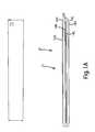
- FIG. 1Ais side elevational view of a printed circuit board (“PCB”) coil in accordance with an embodiment of the present invention.
- PCBprinted circuit board
- FIG. 1Bis an exploded representational perspective view of the traces of the PCB coil.
- FIG. 1Cis an exploded representational perspective view similar to FIG. 1B with select segments shaded to show the path of a single filament.
- FIG. 2Ais a top plan view of the trace of the first layer (or top) of the PCB coil.
- FIG. 2Bis a top plan view of the trace of the second layer of the PCB coil.
- FIG. 2Cis a top plan view of the trace of the third layer of the PCB coil.
- FIG. 2Dis a top plan view of the trace of the fourth (or bottom) layer of the PCB coil.
- FIG. 3is a top plan view of a corner portion of a single spiral trace.
- FIG. 4is a top plan view of a straight portion of a single spiral trace.
- FIG. 5is a perspective view of a portion of an alternative PCB coil showing an alternative construction for minimizing constriction at an interface.
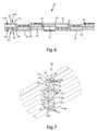
- FIG. 6is a schematic representation of the connection scheme between segments of the various layers.
- FIG. 7is a perspective view of an interchange showing the overlapping arrangement of the segments.
- FIG. 8Ais a top plan view of the top conductor layer of a first alternative PCB coil with upward/downward and inward/outward filament undulations.
- FIG. 8Bis a top plan view of the bottom conductor layer of the first alternative PCB coil.
- FIG. 9is an exploded representational perspective view of a portion of the first alternative PCB coil.
- FIG. 10is a schematic representation of a second alternative PCB coil having three layers and “tripled” traces.
- FIG. 11Ais a top plan view of the top conductor layer of the second alternative PCB coil.
- FIG. 11Bis a top plan view of the middle conductor layer of the second alternative PCB coil.
- FIG. 11Cis a top plan view of the bottom conductor layer of the second alternative PCB coil.
- FIG. 12is an exploded representational perspective view of a portion of the second alternative PCB coil.
- FIG. 13is a schematic representation of a third alternative PCB coil three-layer coil with upward/downward and inward/outward undulations.
- FIG. 14is a schematic representation of a fourth alternative PCB coil.
- FIG. 15Ais a top plan view of the first layer of the fourth alternative PCB coil of FIG. 14 .
- FIG. 15Bis a top plan view of the second layer of the fourth alternative PCB coil of FIG. 14 .
- FIG. 15Cis a top plan view of the third layer of the fourth alternative PCB coil of FIG. 14 .
- FIG. 15Dis a top plan view of the fourth layer of the fourth alternative PCB coil of FIG. 14 .
- FIG. 16is a representation of the connection scheme of the fourth alternative PCB coil of FIG. 14 .
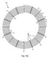
- FIG. 17is a schematic representation of a fifth alternative PCB coil.
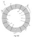
- FIG. 18is a schematic representation of a sixth alternative PCB coil.
- FIGS. 1A , 1 B and 1 CA printed circuit board (“PCB”) coil 20 in accordance with an embodiment of the present invention is shown in FIGS. 1A , 1 B and 1 C.
- the PCB coil 20generally includes a plurality of alternating conductor layers 14 a - d and insulator layers 16 a - c that cooperatively form a multilayer coil (See FIG. 1A ).
- Each conductor layer 14 a - dincludes a trace 52 a - d defined by a plurality of discrete segments 18 (See FIG. 1B ).
- the segments 18 of different traces 52 a - d in different conductor layers 14 a - dare interconnected by connectors 40 to define “filaments” 54 a - d (discrete current flow paths) that undulate through the layers in a predetermined pattern (See FIGS. 1C , 6 and 7 ).
- the predetermined patternis designed so that there will be a substantially even distribution of power induced among the filaments 54 a - d when the PCB coil is paired with a second inductive coil 15 .
- the PCB coil 20simulates a litz wire coil in that the filaments 54 a - d , though offset, follow substantially parallel undulations through the conductor layers 14 a - d .
- the filaments 54 a - dfollow substantially regular, repeating undulations with each filament 54 a - d spending substantially the same amount of total time on each layer 14 a - d of the PCB coil 20 .
- the undulationsoccur frequently enough that all of the filaments 54 a - d intercept a substantially equal amount of magnetic flux lines from the paired coil 15 , and therefore inductively generate substantially equal amounts of power and represent substantially equal amounts of inductance.
- each filament 54 a - dpasses through each layer approximately 4 times, but the number of undulations may vary from application to application.
- the present inventionis well-suited and readily adapted for use with PCB coils with different numbers of layers. For example, a greater or smaller number of layers may be used to provide a coil with the desired characteristics. In applications with a greater number of layers, the segment connection patterns disclosed herein can be carried forward into additional layers or alternative connection schemes can be developed.
- the size, shape and configuration of the traces and segments in each layermay be varied to provide a PCB coil of the desired characteristics.
- the present inventionis illustrated in connection with a generally oval coil.
- the shape of the coilmay vary from application to application as desired.
- the present inventioncan be implemented in circular, rectangular, square and irregular shaped coils.
- the present inventionis shown in connection with a coreless PCB coil.
- the present inventioncan be incorporated into a paired set of coils that include a core, such as a magnetic core.
- the PCB coilmay define an aperture within the center of the coil of sufficient size to receive a core (not shown).
- the coremay be separately manufactured and mounted within the aperture during assembly.
- a layer of magnetic materialsuch as, for example, ferromagnetic or ferrimagnetic material, may be incorporated into the PCB substrate so that the PCB substrate effectively functions as a barrier to stray electromagnetic field.
- the present inventionmay be incorporated into flexible circuit board design.
- flexible conductor layers and insulator layersmay be disposed on a flexible substrate.
- the flexible circuit designmay also include a flexible amorphous magnetic core material.
- the electrical/electronic components to be used in association with the PCB coilmay be populated on the same PCB assembly that carries the PCB coil.
- the present inventionmay be used in place of a wire coil or a conventional PCB coil in essentially any application.
- the PCB coilmay replace both coils in a coupled pair of coils.
- the PCB coilmay be used in conjunction with conventional coils, such as conventional wire coils or conventional PCB coils.
- directional termssuch as “top,” “bottom,” “upper” and “lower” are used to denote directions relative to the orientation of the PCB coil shown in the figures.
- terms such as “inward” and “outward”are used to denote directions toward and away from the center of the coil.
- the PCB coil 20is incorporated into a multilayer circuit board 12 .
- the multilayer circuit board 12may be manufactured in accordance with any suitable techniques and apparatus for manufacturing multilayer circuit boards, including both rigid and flexible circuit board constructions.
- the PCB coil 20 of FIG. 1Bis defined by a plurality of conductor layers 14 a - d that are spaced apart from one another by insulator layers 16 a - c .
- the conductor layers 14 a - d and insulator layers 16 a - cmay be essentially any materials suitable for use in the manufacture of multilayer circuit boards.
- each conductor layer 14 a - dis formed by a thin copper layer deposited on one major surface of a layer of circuit board substrate material, such as fiberglass.
- Conductor layerscan be deposited on both major surfaces of a layer of circuit board substrate material so that two traces can be applied to a single layer of circuit board substrate material. In applications where more than two conductor layers are desired, additional traces can be disposed on additional layers of circuit board substrate material.
- the layers of circuit board substrate materialcan be stacked together to form the multilayer PCB. When a plurality of circuit board substrate material layers are included, adjacent layers may be separated by an additional insulative layer, such as a thin layer of fiberglass.
- the various conductive and insulative layers of the PCB coilcan be heated and pressed together to form a single multilayer PCB, if desired.
- the multilayer PCBmay be manufactured using conventional lamination techniques and apparatus.
- the PCB coilmay be manufactured using a stack of separate printed circuit board substrates that are spaced apart by insulative layers and are mechanically interconnected, for example, by screws (not shown).
- the conductor layers 14 a - dinclude generally identical traces 52 a - d .
- FIGS. 2A-2Dshow the traces 52 a - d for a four-layer PCB coil 20 manufactured in accordance with an embodiment of the present invention.
- FIG. 2Ashows a spiral trace 52 a of the first, and uppermost, layer of the PCB coil 20 .
- FIG. 2Bshows the spiral trace 52 b for the second layer.
- FIG. 2Cshows the spiral trace for the third layer.
- FIG. 2Dshows the spiral trace 52 d for the fourth, and lowermost, layer.
- the segments 18may be offset from layer to layer to facilitate interconnection between the segments 18 of different layers.
- the spiral traces 52 a - dare generally identical only the uppermost spiral trace 52 a will described in detail. The remaining traces 52 b - d will be separately addressed to the extent necessary to address deviations from the uppermost trace 52 a that merit specific discussion.
- the uppermost spiral trace 52 aincludes a plurality of conductor segments 18 arranged in a generally oval, spiraling pattern.
- the segments 18 in this trace 52 aare elongated sections of electrically conductive material that are spaced apart from one another so that they are all electrically isolated (See, for example, FIGS. 2A-2D ).
- Each of the remaining traces 52 b - dincludes a substantially identical arrangement of segments 18 .
- the traces 52 a - dare substantially coextensive.
- the segments 18 of different conductor layers 14 a - dare electrically interconnected by a plurality of connectors 40 that chain the segments 18 together to define filaments 54 a - d (described in more detail below).
- interlayer connectors 40are disposed at interchanges 22 located at opposite ends of each segment 18 .
- the traces 52 a - dare configured at the interchanges 22 so that the segments 18 overlap to permit the use of essentially conventional vias 24 for interconnecting segments 18 in different layers.
- the lowermost layer of the illustrated embodimentincludes an interchange with a more complex shape.
- the lowermost interchangeincludes bypass portions 60 and 62 that facilitate connection of the outer end of the lowermost layer segment 18 with the inner end of the uppermost segment.
- the vias 24are arranged to extend vertically between layers 14 a - d from segment to segment in an arranged pattern as described in more detail below.
- Each via 24generally includes an aperture 26 defined through the insulating materials and a conductor 28 extending through the aperture 26 to provide a current flow path through the insulating materials.
- the vias 24may be formed by drilling through the circuit board stack to form the apertures 26 and then plating the apertures 26 with copper to form the conductors 28 . For example, electroplating, electrolessplating or other plating techniques may be used.
- each via 24may extend vertically through all of the layers 14 a - d , the vias 24 are connected only to those segments 18 where an electrical connection is required to create the desired current flow pattern.
- the via aperture drilling processwill expose a portion of the segment 18 within the via aperture 26 . Accordingly, when the conductor 28 is added to the via 24 (e.g. the drilled hole is electroplated with copper), an electrical connection will be made between the segment 18 and the via 24 . With segments 18 where an electrical connection is not desired, the segment 18 may define an isolation aperture 42 that isolates the segment 18 from the via 24 . As shown in FIG. 7 , the isolation aperture 42 is concentric with the via aperture 24 and has a diameter greater than the corresponding via aperture 26 . Because the isolation aperture 42 has a greater diameter than the via aperture 26 , the conductor 28 will not make an electrical connection with the segment 18 .
- the conductors 28 in the illustrated vias 24are formed by electroplated copper, the conductors 28 may be formed by other conductive materials.
- a conductor materialsuch as a segment of wire, may be press-fitted through the via apertures 24 in the PCB coil 20 (not shown).
- the via apertures 24may be filled with solder to define the conductors 28 (not shown).
- the interchanges 22may have a special shape. For example, as perhaps best shown in FIGS. 3 and 4 , enlarged portions 44 of each trace may be provided around the isolation apertures 42 and vias 24 to provide additional conductor area for current flow. In the illustrated embodiment, the traces are enlarged around the isolation apertures 42 to a degree where it is desirable to provide reduced width of portions 46 in the trace in adjacent loops.
- An alternative interchange constructionis shown in FIG. 5 . In this alternative construction, each trace is enlarged around each isolation aperture 42 , but not each via 24 . The enlarged regions are not strictly necessary and may be eliminated, if desired.
- the spacing between adjacent loopsmay be great enough to avoid the need to reduce the width of portions of the trace in adjacent loops.
- the affect on resistance caused by removal of conductor material for the isolation apertures 42may not be sufficient to warrant enlarged regions in the traces 52 a - d.
- FIG. 1Cshows traces 52 a - d with the segments 18 of a single filament (i.e. filament 54 a ) shaded.
- the shaded segments 18are numbered consecutively from S 1 to S 78 to show the order in which the segments are electrically connected. For example, segment S 1 of trace 52 a is electrically connected to segment S 2 of trace 52 b , segment S 2 is electrically connected to segment S 3 of trace 52 c and so on through segment S 78 .
- FIG. 6shows a schematic representation of the electrical connection scheme of the illustrated embodiment of the present invention showing portions of all four filaments 54 a - d , which each filament 54 a - d having different shading.
- the illustrationrepresents a side view of a seven-segment long portion of the coil 20 , and shows the segments 18 of different layers interconnected by interlayer connectors 40 .
- the illustrated connection schemeis intended to provide a coil in which the filaments spend substantially equal amounts of time in proximity to the paired coil (e.g.
- the filaments 54 a - deach intercept a substantially equal amount of magnetic flux lines, thereby inductively generating a substantially equal amount of current and contributing substantially equally to the self or mutual inductance of the coil.
- Thisprovides substantially uniform distribution of current flow through the different filaments, thereby reducing losses and improving overall efficiency of the PCB coil 20 .
- These benefitsare provided in part by decreasing the capacitance in the coil. Instead of the relatively large parasitic capacitance generated due to the surface area of stacked coils separated by a distance, a relatively smaller parasitic capacitance is generated by the smaller surface area of segments separated by a distance.
- the PCB coil 20simulates a litz wire coil, but the PCB coil is thinner and allows for tighter coupling than a litz wire coil that is hampered by its packing density.
- the connection schememay vary from application to application depending on the design and configuration of the PCB coil and the paired coil.
- the PCB coil 20includes segments 18 that are interconnected to define four filaments (or separate current flow paths) that undulate from layer to layer 14 a - d through the spiral traces and have a substantially equal amount of segments 18 on each layer 14 a - d .
- the different filaments 54 a - dare represented in FIG. 6 by different shading. All of the segments 18 and connectors 40 that define filament 54 a are numbered in FIG. 6 . To avoid clutter, only one segment 18 of each of the remaining filaments 54 c - d is numbered. Like filament 54 a , the remaining filaments 54 b - d are defined by all segments 18 of the same shading and all connectors 40 interconnecting segments 18 of the same shading.
- each segment 18will be defined as having an inner end 18 a and an outer end 18 b .
- the inner end 18 ais the end closest to the center of the spiral and the outer end 18 b the end farthest from the center of the spiral.
- the inner end 18 a of each segmentis electrically connected to the outer end 18 b of the segment in the immediately underlying layer, with one exception.
- each filament 54 a - ddrops down one layer 14 a - d as it moves one segment 18 closer to the innermost end of the coil.
- a filament 54 a - dreaches the bottom layer 14 d it jumps back to the top layer 14 a while moving one segment 18 closer to the innermost end of the coil and then repeats the single layer descension pattern. This pattern repeats itself for each filament 54 a - d through the length of the spiral coil.
- each filament 54 a - dundulates repeatedly between the top layer 14 a and bottom layer 14 d passing sequentially through each intermediate layer 14 b and 14 c as it transitions.
- the different filaments 54 a - dfollow essentially parallel (but offset) paths as they undulate through the PCB coil 20 .
- the specific segment and connection patternmay be varied from application to application as desired with the goal of presenting a coil in which each filament 54 a - d inductively receives a substantially equal amount of power from the paired coil and contributes sufficiently equally to the self or mutual inductance characteristics of the inductive coupling.
- the patternmay be reversed with each filament passing layer by layer upwardly to the uppermost layer and then returning to the bottommost layer.
- PCB coil 20includes a plurality of filaments that undulate upwardly/downwardly through the layers as they spiral inwardly through the coil 20 .
- the PCB coil 220may be configured to additionally provide inward/outward undulation of the filaments within each layer.
- FIGS. 8A-8B and 9show an alternative embodiment of the present invention that provides both upward/downward and inward/outward undulations.
- the PCB coil 220includes two conductor layers 202 a - b separated by an insulator layer (not shown). Referring now to FIGS.
- each conductor layer 202 a - bmay include two adjacent, segmented traces 206 a and 206 b in the form of substantially parallel lines that spiral in a paired relationship.
- the PCB coil 220includes interlayer connectors 210 (See FIG. 9 ) and intralayer connectors 212 that collectively connect the segments 214 of different layers 202 a - b and different traces 206 a and 206 b to define four separate filaments 208 a - d.
- the interlayer connectors 210connect the segments 214 of the paired layers 202 a - b to provide upward/downward undulation of the filaments 208 a - d .
- FIG. 9shows both layers 202 a - b and both traces 206 a - b for a portion of PCB coil 210 .
- the interlayer connectors 210are represented in FIG. 9 by lines, but it should be understood that the interlayer connectors 210 may be conventional vias or other conductors capable of providing an electrical connection between segments 214 of different layers 202 a - b .
- the interlayer connectors 210may be essentially identical to the interlayer connectors discussed above, and may each include an interchange 216 and one or more vias 218 .
- the intralayer connectors 212 of this embodimentconnect segments 214 within the same layer 202 a - b .
- the intralayer connectors 212may be integral with the traces 206 a - b .
- segments 214 in different traces 206 a - bmay be integrally joined by the same conductor material used to form the segments 214 .
- the segments 214may be joined by separate electrical connectors added to the construction.
- the PCB coil segments 214are connected in a pattern to define a plurality of filaments 208 a - d that undulate upwardly/downwardly and inwardly/outwardly.
- the patternmay be selected so that each filament 208 a - d spends substantially the same amount of time in proximity to a paired coil (not shown). This may be achieved, for example, by having each filament 208 a - b undulate in a regular, repeating pattern such that each filament spends substantially the same amount of time on each layer and in each of the traces.
- the frequency of the undulationsmay be selected to provide the desired degree of uniformity between the filaments 208 a - d .
- FIGS. 8A-8Buse reference numbers to represent the interlayer connectors 210 .
- two like reference numbersrepresent opposite ends of an interlayer connector 210 .
- reference numbers A and A′represent opposite ends of an interlayer connector 210 electrically connecting the two corresponding segments 214 and reference numbers B and B′ represent opposite ends of another interlayer connector 210 .
- FIGS. 10 , 11 A- 11 C and 12show a second alternative coil 320 with three layers 302 a - c and “tripled” traces 304 a - c (e.g. three traces that spiral together).
- FIG. 10shows a representational cross-sectional view illustrating the connections 306 that may be included in a PCB coil with three layers and “tripled” traces. Each arrow in FIG. 10 represents a connection from the outer end of one segment 314 to the inner end of the next segment 314 .
- FIGS. 11A-11Cshow traces of the three layers 302 a - c of one implementation of PCB coil 320 .
- FIGS. 11A-11Cuse essentially the same convention described above in connection with FIGS. 8A-8B to show the interlayer connectors 310 of PCB coil 320 .
- reference numbers A and A′represent opposite ends of an interlayer connector 310 electrically connecting the two corresponding segments 314 and reference numbers B and B′ represent opposite ends of another interlayer connector 310 .
- the segment connectionsare further illustrated in FIG. 12 .
- FIG. 12shows all three layers and all three traces for a portion of PCB coil 320 .
- FIG. 12also shows interlayer connectors 310 and intralayer connectors 312 .
- FIG. 13illustrates another alternative coil configuration using essentially the same illustration convention used in connection with FIG. 10 (described above).
- the coil 520includes three conductor layers 502 a - c that are separated by insulator layers (not shown).
- the uppermost layer 502 aincludes “tripled” traces 504 a - c
- the second layer 502 bincludes “quadrupled” traces 506 a - d
- the lowermost layer 502 cincludes “tripled” traces 508 a - c .
- the second layer 502 bis configured with traces 506 a - d that are vertically aligned with the gaps between the traces 504 a - c and 508 a - c of the uppermost layer 502 a and the lowermost layer 502 c .
- the traces 504 a - c , 506 a - d and 508 a - coverlap so that there is not an open vertical path through the PCB coil 520 .
- the use of overlapping traces across the layersmay improve the efficiency of the PCB coil 520 by reducing or eliminating any potential gaps through which magnetic flux may pass vertically without being intercepted by a conductor layer.
- FIG. 14is a schematic representation of another alternative printed circuit board coil 620 .
- the coil 620 of this embodimentincludes an alternative interchange configuration that provides reduced resistance and reduced capacitance. This illustration shows the layers 602 a - d of the coil 620 positioned one atop another with the segments 618 represented by boxes and the vias represented by lines interconnecting the boxes.
- the coil 620includes four layers 602 a - d with each layer 602 a - d having a single segmented trace 604 a - d .
- the interchange schemeprovides the coil 620 with filaments 608 a - d that undulate upwardly/downwardly from layer to layer as they spiral inwardly/outwardly along traces 604 a - d .
- each filament 608 a - dis represented by a plurality of connected boxes that share common shading.
- the coil 620includes four filaments 608 a - d that move upwardly/downwardly no more than a single layer at a time.
- the filament 608 abegins in layer 602 a transitions down to layer 602 b at the first interchange 622 a , down to layer 602 c at the second interchange 622 b and finally down to layer 602 d at the third interchange 622 c .
- the filament 608 aremains on the bottom layer 602 d through the fourth interchange 622 d .
- the filament 608 abegins its transition back toward the first layer 602 a .
- the filament 608 atransitions up to layer 602 c at the fifth interchange 622 e , up to layer 602 b at the sixth interchange 622 f and finally back to the top layer 602 a at the seventh interchange 622 g .
- the filament 608 aremains on the top layer 602 a through the next interchange (in this case, the eighth interchange) and then repeats the cycle over and over again until the opposite end of the coil is reached.
- the remaining filaments 608 b - dfollow essentially identical and parallel paths through the coil being offset from one another because they start at different layers 602 b - d in the coil 620 .
- FIGS. 15A-Dshow the four traces 604 a - d of the coil 620 .
- the four traces 604 a - dare shown in the same orientation so that the illustrations may be overlayed to show their alignment in the assembled coil 620 .
- the first two traces 604 a - bmay be disposed on opposite sides of a single circuit board substrate, while the second two traces 604 c - d may be disposed on opposite sides of a second circuit board substrate.
- the two circuit board substrates carrying the four traces 604 a - dmay be intersecured to form an assembly with four layers 602 a - d and four traces 604 a - d .
- the two circuit board substratesmay be joined together by an adhesive, such as by a layer of epoxy-impregnated fiberglass, or by any other suitable method of manufacture.
- FIG. 16is a representation of a portion of the coil 620 showing corresponding segments of the coil of the four layers 602 a - d illustrated in a side by side arrangement. It should be understood that these four layers are stacked one atop the other in the assembled coil 620 . They are unstacked and placed side-by-side simply to facilitate disclosure.
- the coil 620includes two different types of interchanges that alternate one after another through the length of the coil 620 .
- the first type of interchangeas exemplified by interchanges 622 a and 622 c , includes “blind” vias between layers 602 a and 602 b and between layers 602 c and 602 d .
- the blind viasinterconnect the first segment in layer 602 a with the second segment in layer 602 b , and interconnect the first segment in layer 602 b with the second segment in layer 602 a .
- the blind viasinterconnect the first segment in layer 602 c with the second segment in layer 602 d , and interconnect the first segment in layer 602 b with the second segment in layer 602 c .
- the first type of interchangeelectrically interconnects the first two layers 602 a and 602 b and electrically connects the second two layers 602 c and 602 d .
- the blind viasmay be manufactured by separately drilling holes 626 through the two circuit board substrates, for example, before the two substrates are assembled into the coil 620 .
- the drilled holes 626may be copper plated to provide electrical connections between the top two layers 602 a and 602 b and between the bottom two layers 602 c and 602 d .
- the copper platingmay be applied to the blind vias in the two circuit board substrates while they are separate from one another.
- each layer 602 a - dincludes multiple vias. That is, multiple holes 626 are drilled through each circuit board substrate. As with other embodiments, the drilled holes 626 may be copper plated to provide electrical connections between different layers.
- the second type of interchangeincludes vias that extend entirely through the assembly and electrically interconnect layers 602 b and 602 c .
- the second type of interchangeinterconnects the second segment of layer 602 b with the third segment of layer 602 c , and interconnects the second segment of layer 602 c with the third segment of layer 602 b .
- the second type of interchangeelectrically connects only the middle two layers 602 b and 602 c .
- the second type of interchangemay be manufactured by drilling holes 626 entirely through the assembled coil (e.g. both substrates and the material separating the two substrates) and then applying a copper plating to the holes 626 .
- the traces 604 a and 604 d in the top and bottom layers 602 a and 602 bhave enlarged voids 644 that separate the copper plating in the holes 626 from the traces 604 a and 604 d .
- adjacent voids 644 in the same layermay be offset along the length of the trace, as desired. The offset arrangement reduces the restriction on current flow through the copper plating between the two voids 644 .
- layer 602 cincludes fingers 645 that bridge the distance between the offset voids 644 .
- the fingers 645have reduced cross-sectional area and therefore may prevent some restriction to current flow as compared with portions of the traces that have full cross-sectional area. As a result, it may be desirable to balance the degree of offset between the voids 644 with the corresponding increase in the length of the fingers 645 .
- the traces 604 b and 604 c in the middle two layers 602 b and 602 cdo not include these voids 644 , but rather are in direct electrical connection with the copper plating. As a result, the copper plating interconnects the segments of the second and third layers 602 b and 602 c .
- the coil 620provides the filament undulation pattern described above.
- FIG. 17is a representation of another alternative embodiment in which the interchange configuration of the embodiment of FIG. 14 is carried out in six layers. This representation follows the same conventions used in connection with FIG. 6 and FIG. 14 .
- the coil 720includes three different types of interchanges.
- the first type of interchangeexemplified by interchanges 722 a , 722 d , 722 g and 722 j , provides three sets of blind vias.
- the first set of blind viasinterconnects layers 702 a and 702 b , the second set interconnects layers 702 c and 702 d , the third set interconnects layers 702 e and 702 f .
- the blind viasmay be manufactured in essentially the same way as the blind vias of coil 620 as described above.
- the second type of interchangeas exemplified by interchanges 722 b , 722 e , and 722 h , connects only layers 702 b and 702 c .
- layer 702 bmay include full ends similar to those of layer 602 b at interchange 622 b of FIG. 16
- layer 702 cmay include fingers similar to those of layer 602 c at interchange 622 b of FIG. 16 .
- layers 702 a and 702 d - fmay include voids similar to voids 644 of coil 620 .
- the third type of interchangeas exemplified by interchanges 722 c , 722 f and 722 i , interconnects only layers 702 d and 702 e .
- layer 702 dmay include full ends similar to those of layer 602 b at interchange 622 b of FIG. 16
- layer 702 emay include fingers similar to those of layer 602 c at interchange 622 b of FIG. 16 .
- layers 702 a - c and 702 fmay include voids similar to voids 644 of coil 620 .
- the filaments 708 a - fundulate up and down through the layers 702 a - f no more than one layer at a time.
- a single filament 708 aremains on layer 702 a for a distance equal to approximately three segments, transitions down to layer 702 b for one segment, transitions down to layer 702 c for a distance equal to approximately two segments, transitions down to layer 702 d for a distance equal to approximately two segments, transitions down to layer 702 e for one segment and then transitions to layer 702 f for a distance equal to approximately three segments.
- the filament 708 athen follows the same pattern (although in mirror) as it transitions one layer at a time back to the top layer.
Landscapes
- Engineering & Computer Science (AREA)
- Power Engineering (AREA)
- Microelectronics & Electronic Packaging (AREA)
- Coils Or Transformers For Communication (AREA)
- Coils Of Transformers For General Uses (AREA)
- Parts Printed On Printed Circuit Boards (AREA)
- Electromagnets (AREA)
Abstract
Description
Claims (26)
Priority Applications (1)
| Application Number | Priority Date | Filing Date | Title |
|---|---|---|---|
| US12/236,832US7973635B2 (en) | 2007-09-28 | 2008-09-24 | Printed circuit board coil |
Applications Claiming Priority (3)
| Application Number | Priority Date | Filing Date | Title |
|---|---|---|---|
| US97595307P | 2007-09-28 | 2007-09-28 | |
| US4429808P | 2008-04-11 | 2008-04-11 | |
| US12/236,832US7973635B2 (en) | 2007-09-28 | 2008-09-24 | Printed circuit board coil |
Publications (2)
| Publication Number | Publication Date |
|---|---|
| US20090085706A1 US20090085706A1 (en) | 2009-04-02 |
| US7973635B2true US7973635B2 (en) | 2011-07-05 |
Family
ID=40507553
Family Applications (1)
| Application Number | Title | Priority Date | Filing Date |
|---|---|---|---|
| US12/236,832Active2028-10-03US7973635B2 (en) | 2007-09-28 | 2008-09-24 | Printed circuit board coil |
Country Status (10)
| Country | Link |
|---|---|
| US (1) | US7973635B2 (en) |
| EP (1) | EP2201826A2 (en) |
| JP (1) | JP2011504289A (en) |
| KR (1) | KR20100057877A (en) |
| CN (1) | CN101810062A (en) |
| AU (1) | AU2008308975A1 (en) |
| CA (1) | CA2697440A1 (en) |
| RU (1) | RU2010116556A (en) |
| TW (1) | TW200938017A (en) |
| WO (1) | WO2009045888A2 (en) |
Cited By (36)
| Publication number | Priority date | Publication date | Assignee | Title |
|---|---|---|---|---|
| US20090212637A1 (en)* | 2008-02-22 | 2009-08-27 | Access Business Group International Llc | Magnetic positioning for inductive coupling |
| US20090230777A1 (en)* | 2008-03-13 | 2009-09-17 | Access Business Group International Llc | Inductive power supply system with multiple coil primary |
| US20110057629A1 (en)* | 2009-09-04 | 2011-03-10 | Apple Inc. | Harnessing power through electromagnetic induction utilizing printed coils |
| DE102011089251A1 (en)* | 2011-12-20 | 2013-06-20 | Siemens Aktiengesellschaft | Tripping unit for actuating a mechanical switching unit of a device |
| US8973252B2 (en) | 2012-09-27 | 2015-03-10 | Toyota Motor Engineering & Manufacturing North America, Inc. | Folded planar Litz wire and method of making same |
| US20150092321A1 (en)* | 2013-10-01 | 2015-04-02 | Abb Technology Ag | Energy supply device for explosion-proof electronic functional units |
| US9272157B2 (en) | 2010-05-02 | 2016-03-01 | Nervive, Inc. | Modulating function of neural structures near the ear |
| US9339645B2 (en) | 2010-05-02 | 2016-05-17 | Nervive, Inc. | Modulating function of the facial nerve system or related neural structures via the ear |
| US9413196B2 (en) | 2012-04-09 | 2016-08-09 | Toyota Motor Engineering & Manufacturing North America, Inc. | Wireless power transfer |
| US9642219B2 (en) | 2014-06-05 | 2017-05-02 | Steelcase Inc. | Environment optimization for space based on presence and activities |
| US9852388B1 (en) | 2014-10-03 | 2017-12-26 | Steelcase, Inc. | Method and system for locating resources and communicating within an enterprise |
| US9921726B1 (en) | 2016-06-03 | 2018-03-20 | Steelcase Inc. | Smart workstation method and system |
| US9955318B1 (en) | 2014-06-05 | 2018-04-24 | Steelcase Inc. | Space guidance and management system and method |
| US10065047B2 (en) | 2013-05-20 | 2018-09-04 | Nervive, Inc. | Coordinating emergency treatment of cardiac dysfunction and non-cardiac neural dysfunction |
| US10144302B2 (en) | 2016-09-23 | 2018-12-04 | Qualcomm Incorporated | Twisted wire for power charging |
| US10161752B1 (en) | 2014-10-03 | 2018-12-25 | Steelcase Inc. | Method and system for locating resources and communicating within an enterprise |
| US10264213B1 (en) | 2016-12-15 | 2019-04-16 | Steelcase Inc. | Content amplification system and method |
| US10353664B2 (en) | 2014-03-07 | 2019-07-16 | Steelcase Inc. | Method and system for facilitating collaboration sessions |
| US10433646B1 (en) | 2014-06-06 | 2019-10-08 | Steelcaase Inc. | Microclimate control systems and methods |
| US10504643B2 (en) | 2016-12-15 | 2019-12-10 | Hamilton Sunstrand Corporation | Electrical device with flexible connectors |
| US10614694B1 (en) | 2014-06-06 | 2020-04-07 | Steelcase Inc. | Powered furniture assembly |
| US10622842B2 (en) | 2011-11-04 | 2020-04-14 | Lg Innotek Co., Ltd. | Wireless power receiver and control method thereof |
| US10692642B2 (en) | 2015-10-27 | 2020-06-23 | Cochlear Limited | Inductance coil with varied geometry |
| US10692643B2 (en) | 2015-10-27 | 2020-06-23 | Cochlear Limited | Inductance coil path |
| US10733371B1 (en) | 2015-06-02 | 2020-08-04 | Steelcase Inc. | Template based content preparation system for use with a plurality of space types |
| US20210210283A1 (en)* | 2018-09-29 | 2021-07-08 | Vivo Mobile Communication Co., Ltd. | Wireless charging coil and terminal device |
| US11122714B2 (en)* | 2018-10-17 | 2021-09-14 | Delta Electronics, Inc. | Power module having metallic heat-dissipation substrate |
| US11123567B2 (en) | 2017-02-07 | 2021-09-21 | Advanced Bionics Ag | Antenna apparatus for use with medical implants |
| US11142067B2 (en)* | 2017-05-09 | 2021-10-12 | Dana Automotive Systems Group, Llc | Differential sensor apparatus and method of use |
| US11170926B2 (en) | 2017-12-04 | 2021-11-09 | Alpha And Omega Semiconductor (Cayman) Ltd. | Isolated coupling structure |
| US11321643B1 (en) | 2014-03-07 | 2022-05-03 | Steelcase Inc. | Method and system for facilitating collaboration sessions |
| US11521778B2 (en)* | 2016-11-09 | 2022-12-06 | Lg Electronics Inc. | Coil substrate |
| US11744376B2 (en) | 2014-06-06 | 2023-09-05 | Steelcase Inc. | Microclimate control systems and methods |
| US11984739B1 (en) | 2020-07-31 | 2024-05-14 | Steelcase Inc. | Remote power systems, apparatus and methods |
| US12118178B1 (en) | 2020-04-08 | 2024-10-15 | Steelcase Inc. | Wayfinding services method and apparatus |
| EP4535380A1 (en) | 2023-10-05 | 2025-04-09 | Delta Electronics, Inc. | Wireless power transfer assembly and system |
Families Citing this family (248)
| Publication number | Priority date | Publication date | Assignee | Title |
|---|---|---|---|---|
| CN101860089B (en) | 2005-07-12 | 2013-02-06 | 麻省理工学院 | wireless non-radiative energy transfer |
| US7825543B2 (en)* | 2005-07-12 | 2010-11-02 | Massachusetts Institute Of Technology | Wireless energy transfer |
| US8115448B2 (en) | 2007-06-01 | 2012-02-14 | Michael Sasha John | Systems and methods for wireless power |
| US9421388B2 (en) | 2007-06-01 | 2016-08-23 | Witricity Corporation | Power generation for implantable devices |
| US9823090B2 (en) | 2014-10-31 | 2017-11-21 | Allegro Microsystems, Llc | Magnetic field sensor for sensing a movement of a target object |
| US7923996B2 (en)* | 2008-02-26 | 2011-04-12 | Allegro Microsystems, Inc. | Magnetic field sensor with automatic sensitivity adjustment |
| US20090213565A1 (en)* | 2008-02-27 | 2009-08-27 | International Business Machines Corporation | Emc shielding for printed circuits using flexible printed circuit materials |
| CN102099958B (en) | 2008-05-14 | 2013-12-25 | 麻省理工学院 | Wireless power transfer including interference enhancement |
| US8400017B2 (en) | 2008-09-27 | 2013-03-19 | Witricity Corporation | Wireless energy transfer for computer peripheral applications |
| US8471410B2 (en) | 2008-09-27 | 2013-06-25 | Witricity Corporation | Wireless energy transfer over distance using field shaping to improve the coupling factor |
| US8569914B2 (en) | 2008-09-27 | 2013-10-29 | Witricity Corporation | Wireless energy transfer using object positioning for improved k |
| US8957549B2 (en) | 2008-09-27 | 2015-02-17 | Witricity Corporation | Tunable wireless energy transfer for in-vehicle applications |
| US8946938B2 (en) | 2008-09-27 | 2015-02-03 | Witricity Corporation | Safety systems for wireless energy transfer in vehicle applications |
| US9744858B2 (en) | 2008-09-27 | 2017-08-29 | Witricity Corporation | System for wireless energy distribution in a vehicle |
| US8482158B2 (en) | 2008-09-27 | 2013-07-09 | Witricity Corporation | Wireless energy transfer using variable size resonators and system monitoring |
| US8552592B2 (en)* | 2008-09-27 | 2013-10-08 | Witricity Corporation | Wireless energy transfer with feedback control for lighting applications |
| US9544683B2 (en) | 2008-09-27 | 2017-01-10 | Witricity Corporation | Wirelessly powered audio devices |
| US9105959B2 (en) | 2008-09-27 | 2015-08-11 | Witricity Corporation | Resonator enclosure |
| US8643326B2 (en)* | 2008-09-27 | 2014-02-04 | Witricity Corporation | Tunable wireless energy transfer systems |
| US9184595B2 (en) | 2008-09-27 | 2015-11-10 | Witricity Corporation | Wireless energy transfer in lossy environments |
| US8441154B2 (en) | 2008-09-27 | 2013-05-14 | Witricity Corporation | Multi-resonator wireless energy transfer for exterior lighting |
| US8587155B2 (en)* | 2008-09-27 | 2013-11-19 | Witricity Corporation | Wireless energy transfer using repeater resonators |
| US8692410B2 (en) | 2008-09-27 | 2014-04-08 | Witricity Corporation | Wireless energy transfer with frequency hopping |
| US8324759B2 (en)* | 2008-09-27 | 2012-12-04 | Witricity Corporation | Wireless energy transfer using magnetic materials to shape field and reduce loss |
| US8461721B2 (en)* | 2008-09-27 | 2013-06-11 | Witricity Corporation | Wireless energy transfer using object positioning for low loss |
| US9601261B2 (en) | 2008-09-27 | 2017-03-21 | Witricity Corporation | Wireless energy transfer using repeater resonators |
| US8686598B2 (en) | 2008-09-27 | 2014-04-01 | Witricity Corporation | Wireless energy transfer for supplying power and heat to a device |
| US8901779B2 (en) | 2008-09-27 | 2014-12-02 | Witricity Corporation | Wireless energy transfer with resonator arrays for medical applications |
| US8497601B2 (en) | 2008-09-27 | 2013-07-30 | Witricity Corporation | Wireless energy transfer converters |
| US9093853B2 (en) | 2008-09-27 | 2015-07-28 | Witricity Corporation | Flexible resonator attachment |
| US8410636B2 (en) | 2008-09-27 | 2013-04-02 | Witricity Corporation | Low AC resistance conductor designs |
| US9035499B2 (en) | 2008-09-27 | 2015-05-19 | Witricity Corporation | Wireless energy transfer for photovoltaic panels |
| US8476788B2 (en) | 2008-09-27 | 2013-07-02 | Witricity Corporation | Wireless energy transfer with high-Q resonators using field shaping to improve K |
| US9601270B2 (en) | 2008-09-27 | 2017-03-21 | Witricity Corporation | Low AC resistance conductor designs |
| US8669676B2 (en) | 2008-09-27 | 2014-03-11 | Witricity Corporation | Wireless energy transfer across variable distances using field shaping with magnetic materials to improve the coupling factor |
| EP3179640A1 (en)* | 2008-09-27 | 2017-06-14 | WiTricity Corporation | Wireless energy transfer systems |
| US8692412B2 (en)* | 2008-09-27 | 2014-04-08 | Witricity Corporation | Temperature compensation in a wireless transfer system |
| US9577436B2 (en) | 2008-09-27 | 2017-02-21 | Witricity Corporation | Wireless energy transfer for implantable devices |
| US9065423B2 (en) | 2008-09-27 | 2015-06-23 | Witricity Corporation | Wireless energy distribution system |
| US8487480B1 (en) | 2008-09-27 | 2013-07-16 | Witricity Corporation | Wireless energy transfer resonator kit |
| US8933594B2 (en) | 2008-09-27 | 2015-01-13 | Witricity Corporation | Wireless energy transfer for vehicles |
| US8723366B2 (en)* | 2008-09-27 | 2014-05-13 | Witricity Corporation | Wireless energy transfer resonator enclosures |
| US8907531B2 (en) | 2008-09-27 | 2014-12-09 | Witricity Corporation | Wireless energy transfer with variable size resonators for medical applications |
| US8922066B2 (en) | 2008-09-27 | 2014-12-30 | Witricity Corporation | Wireless energy transfer with multi resonator arrays for vehicle applications |
| US8937408B2 (en) | 2008-09-27 | 2015-01-20 | Witricity Corporation | Wireless energy transfer for medical applications |
| US8587153B2 (en) | 2008-09-27 | 2013-11-19 | Witricity Corporation | Wireless energy transfer using high Q resonators for lighting applications |
| US8901778B2 (en) | 2008-09-27 | 2014-12-02 | Witricity Corporation | Wireless energy transfer with variable size resonators for implanted medical devices |
| US9106203B2 (en) | 2008-09-27 | 2015-08-11 | Witricity Corporation | Secure wireless energy transfer in medical applications |
| US8928276B2 (en) | 2008-09-27 | 2015-01-06 | Witricity Corporation | Integrated repeaters for cell phone applications |
| US8466583B2 (en) | 2008-09-27 | 2013-06-18 | Witricity Corporation | Tunable wireless energy transfer for outdoor lighting applications |
| US8912687B2 (en) | 2008-09-27 | 2014-12-16 | Witricity Corporation | Secure wireless energy transfer for vehicle applications |
| US8963488B2 (en) | 2008-09-27 | 2015-02-24 | Witricity Corporation | Position insensitive wireless charging |
| US9396867B2 (en) | 2008-09-27 | 2016-07-19 | Witricity Corporation | Integrated resonator-shield structures |
| US8461720B2 (en)* | 2008-09-27 | 2013-06-11 | Witricity Corporation | Wireless energy transfer using conducting surfaces to shape fields and reduce loss |
| US8772973B2 (en)* | 2008-09-27 | 2014-07-08 | Witricity Corporation | Integrated resonator-shield structures |
| US9246336B2 (en) | 2008-09-27 | 2016-01-26 | Witricity Corporation | Resonator optimizations for wireless energy transfer |
| US8947186B2 (en) | 2008-09-27 | 2015-02-03 | Witricity Corporation | Wireless energy transfer resonator thermal management |
| US8304935B2 (en)* | 2008-09-27 | 2012-11-06 | Witricity Corporation | Wireless energy transfer using field shaping to reduce loss |
| US9318922B2 (en) | 2008-09-27 | 2016-04-19 | Witricity Corporation | Mechanically removable wireless power vehicle seat assembly |
| US8598743B2 (en) | 2008-09-27 | 2013-12-03 | Witricity Corporation | Resonator arrays for wireless energy transfer |
| US8629578B2 (en) | 2008-09-27 | 2014-01-14 | Witricity Corporation | Wireless energy transfer systems |
| US8461722B2 (en) | 2008-09-27 | 2013-06-11 | Witricity Corporation | Wireless energy transfer using conducting surfaces to shape field and improve K |
| US9515494B2 (en) | 2008-09-27 | 2016-12-06 | Witricity Corporation | Wireless power system including impedance matching network |
| US9601266B2 (en) | 2008-09-27 | 2017-03-21 | Witricity Corporation | Multiple connected resonators with a single electronic circuit |
| US20120091794A1 (en)* | 2008-09-27 | 2012-04-19 | Campanella Andrew J | Wirelessly powered laptop and desktop environment |
| US9160203B2 (en) | 2008-09-27 | 2015-10-13 | Witricity Corporation | Wireless powered television |
| US8362651B2 (en)* | 2008-10-01 | 2013-01-29 | Massachusetts Institute Of Technology | Efficient near-field wireless energy transfer using adiabatic system variations |
| WO2010096367A1 (en) | 2009-02-17 | 2010-08-26 | Allegro Microsystems, Inc. | Circuits and methods for generating a self-test of a magnetic field sensor |
| US9306358B2 (en) | 2009-03-09 | 2016-04-05 | Nucurrent, Inc. | Method for manufacture of multi-layer wire structure for high efficiency wireless communication |
| US11476566B2 (en)* | 2009-03-09 | 2022-10-18 | Nucurrent, Inc. | Multi-layer-multi-turn structure for high efficiency wireless communication |
| US9444213B2 (en) | 2009-03-09 | 2016-09-13 | Nucurrent, Inc. | Method for manufacture of multi-layer wire structure for high efficiency wireless communication |
| US9439287B2 (en) | 2009-03-09 | 2016-09-06 | Nucurrent, Inc. | Multi-layer wire structure for high efficiency wireless communication |
| US9300046B2 (en) | 2009-03-09 | 2016-03-29 | Nucurrent, Inc. | Method for manufacture of multi-layer-multi-turn high efficiency inductors |
| US9208942B2 (en)* | 2009-03-09 | 2015-12-08 | Nucurrent, Inc. | Multi-layer-multi-turn structure for high efficiency wireless communication |
| EP2406655B1 (en) | 2009-03-09 | 2019-01-30 | NuCurrent, Inc. | System and method for wireless power transfer in implantable medical devices |
| US9232893B2 (en) | 2009-03-09 | 2016-01-12 | Nucurrent, Inc. | Method of operation of a multi-layer-multi-turn structure for high efficiency wireless communication |
| DE102009003815A1 (en)* | 2009-04-22 | 2010-10-28 | Wincor Nixdorf International Gmbh | Self-service device |
| KR101673185B1 (en)* | 2009-07-22 | 2016-11-07 | 알레그로 마이크로시스템스, 엘엘씨 | Circuits and methods for generating a diagnostic mode of operation in a magnetic field sensor |
| US8475371B2 (en) | 2009-09-01 | 2013-07-02 | Adidas Ag | Physiological monitoring garment |
| CN102055051B (en)* | 2009-10-30 | 2015-09-30 | 清华大学 | A kind of high-impedance transmission line |
| CN102056070B (en)* | 2009-10-30 | 2016-04-13 | 清华大学 | A kind of hearing aid compatibility test integrated probe |
| TWI391954B (en)* | 2010-01-05 | 2013-04-01 | Hon Hai Prec Ind Co Ltd | Highly-resistant transmission line |
| US8299883B2 (en)* | 2010-03-25 | 2012-10-30 | Hamilton Sundstrand Corporation | Laminated inductive device |
| US9602168B2 (en) | 2010-08-31 | 2017-03-21 | Witricity Corporation | Communication in wireless energy transfer systems |
| US8519251B2 (en) | 2010-10-29 | 2013-08-27 | Anaren, Inc. | Magnetic instrument pickup |
| JP5654367B2 (en)* | 2011-01-28 | 2015-01-14 | パナソニックIpマネジメント株式会社 | Power supply module of non-contact power supply device, method of using power supply module of non-contact power supply device, and method of manufacturing power supply module of non-contact power supply device |
| WO2012105897A1 (en)* | 2011-02-02 | 2012-08-09 | Delaval Holding Ab | Electromagnetic monitoring unit for a liquid substance |
| WO2012107490A2 (en) | 2011-02-09 | 2012-08-16 | Conductix-Wampfler Ag | Apparatus for power transmission and for inductive communication |
| DE102011010792A1 (en)* | 2011-02-09 | 2012-08-09 | Conductix-Wampfler Ag | Device for energy transmission and enabling inductive communication of moving objects, has communication unit connected with inductance unit and provided with modem operated according to orthogonal frequency-division multiplexing |
| DE102011010793A1 (en)* | 2011-02-09 | 2012-08-09 | Conductix-Wampfler Ag | Use of modem in communication device for inductive communication with track-guided or rail-guided movable object via untwisted symmetrical two wire line, using communication inductor connected with communication device |
| US9225392B2 (en) | 2011-03-09 | 2015-12-29 | Qualcomm Incorporated | Flat power coil for wireless charging applications |
| US8680846B2 (en) | 2011-04-27 | 2014-03-25 | Allegro Microsystems, Llc | Circuits and methods for self-calibrating or self-testing a magnetic field sensor |
| CN103782336A (en)* | 2011-06-15 | 2014-05-07 | 安伦股份有限公司 | Improved Magnetic Instrument Pickups |
| US9948145B2 (en) | 2011-07-08 | 2018-04-17 | Witricity Corporation | Wireless power transfer for a seat-vest-helmet system |
| US8604777B2 (en) | 2011-07-13 | 2013-12-10 | Allegro Microsystems, Llc | Current sensor with calibration for a current divider configuration |
| CN108110907B (en) | 2011-08-04 | 2022-08-02 | 韦特里西提公司 | Tunable wireless power supply architecture |
| EP2754222B1 (en) | 2011-09-09 | 2015-11-18 | Witricity Corporation | Foreign object detection in wireless energy transfer systems |
| US20130062966A1 (en) | 2011-09-12 | 2013-03-14 | Witricity Corporation | Reconfigurable control architectures and algorithms for electric vehicle wireless energy transfer systems |
| US9318257B2 (en) | 2011-10-18 | 2016-04-19 | Witricity Corporation | Wireless energy transfer for packaging |
| CA2853824A1 (en) | 2011-11-04 | 2013-05-10 | Witricity Corporation | Wireless energy transfer modeling tool |
| DE102011088394B4 (en) | 2011-12-13 | 2024-11-28 | Robert Bosch Gmbh | metal sensor |
| JP2015508987A (en) | 2012-01-26 | 2015-03-23 | ワイトリシティ コーポレーションWitricity Corporation | Wireless energy transmission with reduced field |
| US9201122B2 (en) | 2012-02-16 | 2015-12-01 | Allegro Microsystems, Llc | Circuits and methods using adjustable feedback for self-calibrating or self-testing a magnetic field sensor with an adjustable time constant |
| US20130214890A1 (en) | 2012-02-20 | 2013-08-22 | Futurewei Technologies, Inc. | High Current, Low Equivalent Series Resistance Printed Circuit Board Coil for Power Transfer Application |
| US9817078B2 (en) | 2012-05-10 | 2017-11-14 | Allegro Microsystems Llc | Methods and apparatus for magnetic sensor having integrated coil |
| CN102693832A (en)* | 2012-06-25 | 2012-09-26 | 江苏中容科技有限公司 | Method for coiling multi-foil lap coil of transformer |
| US9343922B2 (en) | 2012-06-27 | 2016-05-17 | Witricity Corporation | Wireless energy transfer for rechargeable batteries |
| US9287607B2 (en) | 2012-07-31 | 2016-03-15 | Witricity Corporation | Resonator fine tuning |
| KR101883011B1 (en)* | 2012-08-08 | 2018-07-27 | 삼성전기주식회사 | Filter for Removing Noise |
| IN2015DN02392A (en)* | 2012-09-12 | 2015-09-04 | Genesis Group Inc | |
| US9595378B2 (en) | 2012-09-19 | 2017-03-14 | Witricity Corporation | Resonator enclosure |
| EP2909912B1 (en) | 2012-10-19 | 2022-08-10 | WiTricity Corporation | Foreign object detection in wireless energy transfer systems |
| US9842684B2 (en) | 2012-11-16 | 2017-12-12 | Witricity Corporation | Systems and methods for wireless power system with improved performance and/or ease of use |
| US20140167786A1 (en)* | 2012-12-14 | 2014-06-19 | Schneider Electric USA, Inc. | Current Sensor For Power Measurement Applications |
| AU2013203801A1 (en) | 2012-12-15 | 2014-07-03 | JENKINS III, Arthur L. DR | Multilayered Electromagnetic Assembly |
| US9383425B2 (en) | 2012-12-28 | 2016-07-05 | Allegro Microsystems, Llc | Methods and apparatus for a current sensor having fault detection and self test functionality |
| EP2775565A1 (en)* | 2013-03-06 | 2014-09-10 | NuCurrent, Inc. | Multi-layer wire structure for high efficiency wireless communication |
| EP2775564A1 (en)* | 2013-03-06 | 2014-09-10 | NuCurrent, Inc. | Multi-layer-multi-turn structure for high efficiency wireless communication |
| EP2779181B1 (en)* | 2013-03-12 | 2018-09-26 | NuCurrent, Inc. | Multi-layer-multi-turn structure for high efficiency inductors |
| US10725100B2 (en) | 2013-03-15 | 2020-07-28 | Allegro Microsystems, Llc | Methods and apparatus for magnetic sensor having an externally accessible coil |
| GB2512862A (en) | 2013-04-09 | 2014-10-15 | Bombardier Transp Gmbh | Receiving device with coil of electric line for receiving a magnetic field and for producing electric energy by magnetic induction |
| GB2512859A (en)* | 2013-04-09 | 2014-10-15 | Bombardier Transp Gmbh | Structure of a receiving device for receiving a magnetic field and for producing electric energy by magnetic induction |
| GB2512855A (en) | 2013-04-09 | 2014-10-15 | Bombardier Transp Gmbh | Receiving device for receiving a magnetic field and for producing electric energy by magnetic induction |
| US10145908B2 (en) | 2013-07-19 | 2018-12-04 | Allegro Microsystems, Llc | Method and apparatus for magnetic sensor producing a changing magnetic field |
| US10495699B2 (en) | 2013-07-19 | 2019-12-03 | Allegro Microsystems, Llc | Methods and apparatus for magnetic sensor having an integrated coil or magnet to detect a non-ferromagnetic target |
| US9810519B2 (en) | 2013-07-19 | 2017-11-07 | Allegro Microsystems, Llc | Arrangements for magnetic field sensors that act as tooth detectors |
| US9293245B2 (en)* | 2013-08-05 | 2016-03-22 | Qualcomm Mems Technologies, Inc. | Integration of a coil and a discontinuous magnetic core |
| US9857821B2 (en) | 2013-08-14 | 2018-01-02 | Witricity Corporation | Wireless power transfer frequency adjustment |
| GB201322478D0 (en)* | 2013-12-18 | 2014-02-05 | Gyo Gym Ltd | Improvements in or relating to generating your own power |
| EP3080627B1 (en) | 2013-12-26 | 2020-10-14 | Allegro MicroSystems, LLC | Methods and apparatus for sensor diagnostics |
| US9780573B2 (en) | 2014-02-03 | 2017-10-03 | Witricity Corporation | Wirelessly charged battery system |
| US9952266B2 (en) | 2014-02-14 | 2018-04-24 | Witricity Corporation | Object detection for wireless energy transfer systems |
| KR20160145694A (en) | 2014-04-16 | 2016-12-20 | 위트리시티 코포레이션 | Wireless energy transfer for mobile device applications |
| US9892849B2 (en) | 2014-04-17 | 2018-02-13 | Witricity Corporation | Wireless power transfer systems with shield openings |
| US9645220B2 (en) | 2014-04-17 | 2017-05-09 | Allegro Microsystems, Llc | Circuits and methods for self-calibrating or self-testing a magnetic field sensor using phase discrimination |
| US9842687B2 (en) | 2014-04-17 | 2017-12-12 | Witricity Corporation | Wireless power transfer systems with shaped magnetic components |
| DE102014207890A1 (en)* | 2014-04-28 | 2015-07-30 | Continental Automotive Gmbh | Foreign object detection device and power inductive charging device |
| US9735773B2 (en) | 2014-04-29 | 2017-08-15 | Allegro Microsystems, Llc | Systems and methods for sensing current through a low-side field effect transistor |
| US9837860B2 (en) | 2014-05-05 | 2017-12-05 | Witricity Corporation | Wireless power transmission systems for elevators |
| JP2017518018A (en) | 2014-05-07 | 2017-06-29 | ワイトリシティ コーポレーションWitricity Corporation | Foreign object detection in wireless energy transmission systems |
| US9954375B2 (en) | 2014-06-20 | 2018-04-24 | Witricity Corporation | Wireless power transfer systems for surfaces |
| CN104022336B (en)* | 2014-06-27 | 2016-05-04 | 北京邮电大学 | A kind of oriented branch coupler of miniaturization |
| KR20160002070A (en) | 2014-06-30 | 2016-01-07 | 엘지이노텍 주식회사 | Case apparatus |
| US10574091B2 (en) | 2014-07-08 | 2020-02-25 | Witricity Corporation | Enclosures for high power wireless power transfer systems |
| CN107258046B (en) | 2014-07-08 | 2020-07-17 | 无线电力公司 | Resonator equalization in wireless power transfer systems |
| EP3180835A4 (en) | 2014-08-12 | 2017-09-13 | PowerbyProxi Limited | System and method for power transfer |
| US20160064137A1 (en)* | 2014-09-02 | 2016-03-03 | Apple Inc. | Capacitively balanced inductive charging coil |
| US9739846B2 (en) | 2014-10-03 | 2017-08-22 | Allegro Microsystems, Llc | Magnetic field sensors with self test |
| DE102014220978A1 (en)* | 2014-10-16 | 2016-04-21 | Robert Bosch Gmbh | Coil arrangement for inductive energy transmission, inductive energy transmission device and method for producing a coil arrangement for inductive energy transmission |
| US9719806B2 (en) | 2014-10-31 | 2017-08-01 | Allegro Microsystems, Llc | Magnetic field sensor for sensing a movement of a ferromagnetic target object |
| US10712403B2 (en) | 2014-10-31 | 2020-07-14 | Allegro Microsystems, Llc | Magnetic field sensor and electronic circuit that pass amplifier current through a magnetoresistance element |
| US9720054B2 (en) | 2014-10-31 | 2017-08-01 | Allegro Microsystems, Llc | Magnetic field sensor and electronic circuit that pass amplifier current through a magnetoresistance element |
| US9823092B2 (en) | 2014-10-31 | 2017-11-21 | Allegro Microsystems, Llc | Magnetic field sensor providing a movement detector |
| US9841485B2 (en) | 2014-11-14 | 2017-12-12 | Allegro Microsystems, Llc | Magnetic field sensor having calibration circuitry and techniques |
| US9804249B2 (en) | 2014-11-14 | 2017-10-31 | Allegro Microsystems, Llc | Dual-path analog to digital converter |
| US10466298B2 (en) | 2014-11-14 | 2019-11-05 | Allegro Microsystems, Llc | Magnetic field sensor with shared path amplifier and analog-to-digital-converter |
| US9843217B2 (en) | 2015-01-05 | 2017-12-12 | Witricity Corporation | Wireless energy transfer for wearables |
| US9638764B2 (en) | 2015-04-08 | 2017-05-02 | Allegro Microsystems, Llc | Electronic circuit for driving a hall effect element with a current compensated for substrate stress |
| US9851417B2 (en) | 2015-07-28 | 2017-12-26 | Allegro Microsystems, Llc | Structure and system for simultaneous sensing a magnetic field and mechanical stress |
| US9941729B2 (en) | 2015-08-07 | 2018-04-10 | Nucurrent, Inc. | Single layer multi mode antenna for wireless power transmission using magnetic field coupling |
| US9960629B2 (en) | 2015-08-07 | 2018-05-01 | Nucurrent, Inc. | Method of operating a single structure multi mode antenna for wireless power transmission using magnetic field coupling |
| US10063100B2 (en) | 2015-08-07 | 2018-08-28 | Nucurrent, Inc. | Electrical system incorporating a single structure multimode antenna for wireless power transmission using magnetic field coupling |
| US9941743B2 (en) | 2015-08-07 | 2018-04-10 | Nucurrent, Inc. | Single structure multi mode antenna having a unitary body construction for wireless power transmission using magnetic field coupling |
| US10658847B2 (en) | 2015-08-07 | 2020-05-19 | Nucurrent, Inc. | Method of providing a single structure multi mode antenna for wireless power transmission using magnetic field coupling |
| US9960628B2 (en) | 2015-08-07 | 2018-05-01 | Nucurrent, Inc. | Single structure multi mode antenna having a single layer structure with coils on opposing sides for wireless power transmission using magnetic field coupling |
| US9948129B2 (en) | 2015-08-07 | 2018-04-17 | Nucurrent, Inc. | Single structure multi mode antenna for wireless power transmission using magnetic field coupling having an internal switch circuit |
| US10636563B2 (en) | 2015-08-07 | 2020-04-28 | Nucurrent, Inc. | Method of fabricating a single structure multi mode antenna for wireless power transmission using magnetic field coupling |
| US9941590B2 (en) | 2015-08-07 | 2018-04-10 | Nucurrent, Inc. | Single structure multi mode antenna for wireless power transmission using magnetic field coupling having magnetic shielding |
| US11205848B2 (en) | 2015-08-07 | 2021-12-21 | Nucurrent, Inc. | Method of providing a single structure multi mode antenna having a unitary body construction for wireless power transmission using magnetic field coupling |
| US10985465B2 (en) | 2015-08-19 | 2021-04-20 | Nucurrent, Inc. | Multi-mode wireless antenna configurations |
| US10248899B2 (en) | 2015-10-06 | 2019-04-02 | Witricity Corporation | RFID tag and transponder detection in wireless energy transfer systems |
| US9929721B2 (en) | 2015-10-14 | 2018-03-27 | Witricity Corporation | Phase and amplitude detection in wireless energy transfer systems |
| WO2017070227A1 (en) | 2015-10-19 | 2017-04-27 | Witricity Corporation | Foreign object detection in wireless energy transfer systems |
| WO2017070009A1 (en) | 2015-10-22 | 2017-04-27 | Witricity Corporation | Dynamic tuning in wireless energy transfer systems |
| US10075019B2 (en) | 2015-11-20 | 2018-09-11 | Witricity Corporation | Voltage source isolation in wireless power transfer systems |
| WO2017136491A1 (en) | 2016-02-02 | 2017-08-10 | Witricity Corporation | Controlling wireless power transfer systems |
| CN114123540B (en) | 2016-02-08 | 2024-08-20 | 韦特里西提公司 | Variable capacitance device and high-power wireless energy transmission system |
| US10107873B2 (en) | 2016-03-10 | 2018-10-23 | Allegro Microsystems, Llc | Electronic circuit for compensating a sensitivity drift of a hall effect element due to stress |
| US10132879B2 (en) | 2016-05-23 | 2018-11-20 | Allegro Microsystems, Llc | Gain equalization for multiple axis magnetic field sensing |
| US10041810B2 (en) | 2016-06-08 | 2018-08-07 | Allegro Microsystems, Llc | Arrangements for magnetic field sensors that act as movement detectors |
| US10260905B2 (en) | 2016-06-08 | 2019-04-16 | Allegro Microsystems, Llc | Arrangements for magnetic field sensors to cancel offset variations |
| US10012518B2 (en) | 2016-06-08 | 2018-07-03 | Allegro Microsystems, Llc | Magnetic field sensor for sensing a proximity of an object |
| US10162017B2 (en) | 2016-07-12 | 2018-12-25 | Allegro Microsystems, Llc | Systems and methods for reducing high order hall plate sensitivity temperature coefficients |
| US20180062434A1 (en) | 2016-08-26 | 2018-03-01 | Nucurrent, Inc. | Wireless Connector Receiver Module Circuit |
| US10432031B2 (en) | 2016-12-09 | 2019-10-01 | Nucurrent, Inc. | Antenna having a substrate configured to facilitate through-metal energy transfer via near field magnetic coupling |
| US11502547B2 (en) | 2017-02-13 | 2022-11-15 | Nucurrent, Inc. | Wireless electrical energy transmission system with transmitting antenna having magnetic field shielding panes |
| EP3596835B1 (en)* | 2017-03-17 | 2022-06-08 | Efficient Power Conversion Corporation | Antenna with large area scalable highly resonant wireless power coil |
| US10002317B1 (en)* | 2017-04-10 | 2018-06-19 | Brady Worldwide, Inc. | Label with graphene layer and system for authentication of label |
| US10324141B2 (en) | 2017-05-26 | 2019-06-18 | Allegro Microsystems, Llc | Packages for coil actuated position sensors |
| US10996289B2 (en) | 2017-05-26 | 2021-05-04 | Allegro Microsystems, Llc | Coil actuated position sensor with reflected magnetic field |
| US10310028B2 (en) | 2017-05-26 | 2019-06-04 | Allegro Microsystems, Llc | Coil actuated pressure sensor |
| US10641842B2 (en) | 2017-05-26 | 2020-05-05 | Allegro Microsystems, Llc | Targets for coil actuated position sensors |
| US11428755B2 (en) | 2017-05-26 | 2022-08-30 | Allegro Microsystems, Llc | Coil actuated sensor with sensitivity detection |
| US10837943B2 (en) | 2017-05-26 | 2020-11-17 | Allegro Microsystems, Llc | Magnetic field sensor with error calculation |
| US11283295B2 (en) | 2017-05-26 | 2022-03-22 | Nucurrent, Inc. | Device orientation independent wireless transmission system |
| US12159745B2 (en)* | 2017-05-30 | 2024-12-03 | InductEV, Inc. | Wireless power transfer thin profile coil assembly |
| WO2019006376A1 (en) | 2017-06-29 | 2019-01-03 | Witricity Corporation | Protection and control of wireless power systems |
| US10520559B2 (en) | 2017-08-14 | 2019-12-31 | Allegro Microsystems, Llc | Arrangements for Hall effect elements and vertical epi resistors upon a substrate |
| US10172237B1 (en)* | 2017-08-28 | 2019-01-01 | Osram Sylvania Inc. | Space-efficient PCB-based inductor |
| JP7187143B2 (en)* | 2017-10-26 | 2022-12-12 | Tdk株式会社 | coil parts |
| TWI653814B (en) | 2017-12-04 | 2019-03-11 | 英屬開曼群島商萬國半導體(開曼)股份有限公司 | Isolated coupled structure, device, element, a chip including the same, and a printed circuit board |
| US10866117B2 (en) | 2018-03-01 | 2020-12-15 | Allegro Microsystems, Llc | Magnetic field influence during rotation movement of magnetic target |
| KR102554936B1 (en)* | 2018-04-13 | 2023-07-12 | 현대자동차주식회사 | Planar transformer |
| DE102018111715A1 (en) | 2018-05-16 | 2019-11-21 | Beckhoff Automation Gmbh | LINEAR TRANSPORT SYSTEM AND SYSTEM FOR CONTACTLESS ENERGY AND DATA TRANSMISSION |
| CN109148109A (en)* | 2018-07-23 | 2019-01-04 | 浙江省东阳市东磁诚基电子有限公司 | A kind of low-loss FPC loop construction |
| US11255700B2 (en) | 2018-08-06 | 2022-02-22 | Allegro Microsystems, Llc | Magnetic field sensor |
| JP2020027813A (en)* | 2018-08-09 | 2020-02-20 | 矢崎総業株式会社 | Power transmission unit |
| CN109148110B (en)* | 2018-08-20 | 2022-04-19 | 浙江省东阳市东磁诚基电子有限公司 | FPC structure capable of reducing alternating current resistance |
| GB2590331B (en)* | 2018-09-12 | 2022-11-02 | Multi Fineline Electronix Inc | Balanced, symmetrical coil |
| KR20200055426A (en)* | 2018-11-13 | 2020-05-21 | 주식회사 히타치엘지 데이터 스토리지 코리아 | Printed Circuit Board Coil |
| US10823586B2 (en) | 2018-12-26 | 2020-11-03 | Allegro Microsystems, Llc | Magnetic field sensor having unequally spaced magnetic field sensing elements |
| CN109686549B (en)* | 2019-01-11 | 2020-12-29 | 杭州矽磁微电子有限公司 | Integrated transformer with multiple winding coils manufactured through micro-nano processing |
| US11061084B2 (en) | 2019-03-07 | 2021-07-13 | Allegro Microsystems, Llc | Coil actuated pressure sensor and deflectable substrate |
| US10955306B2 (en) | 2019-04-22 | 2021-03-23 | Allegro Microsystems, Llc | Coil actuated pressure sensor and deformable substrate |
| US11227712B2 (en) | 2019-07-19 | 2022-01-18 | Nucurrent, Inc. | Preemptive thermal mitigation for wireless power systems |
| US11271430B2 (en) | 2019-07-19 | 2022-03-08 | Nucurrent, Inc. | Wireless power transfer system with extended wireless charging range |
| US11280637B2 (en) | 2019-11-14 | 2022-03-22 | Allegro Microsystems, Llc | High performance magnetic angle sensor |
| US11237020B2 (en) | 2019-11-14 | 2022-02-01 | Allegro Microsystems, Llc | Magnetic field sensor having two rows of magnetic field sensing elements for measuring an angle of rotation of a magnet |
| US11056922B1 (en) | 2020-01-03 | 2021-07-06 | Nucurrent, Inc. | Wireless power transfer system for simultaneous transfer to multiple devices |
| US11194004B2 (en) | 2020-02-12 | 2021-12-07 | Allegro Microsystems, Llc | Diagnostic circuits and methods for sensor test circuits |
| US11169223B2 (en) | 2020-03-23 | 2021-11-09 | Allegro Microsystems, Llc | Hall element signal calibrating in angle sensor |
| US11516905B2 (en)* | 2020-04-14 | 2022-11-29 | Dell Products L.P. | Method to improve PCB trace conductivity and system therefor |
| US11262422B2 (en) | 2020-05-08 | 2022-03-01 | Allegro Microsystems, Llc | Stray-field-immune coil-activated position sensor |
| US11283303B2 (en) | 2020-07-24 | 2022-03-22 | Nucurrent, Inc. | Area-apportioned wireless power antenna for maximized charging volume |
| US11581755B2 (en) | 2020-07-28 | 2023-02-14 | InductEV, Inc. | Efficiency gains through magnetic field management |
| US11417461B2 (en)* | 2020-10-29 | 2022-08-16 | Google Llc | Techniques and apparatuses to reduce inductive charging power loss |
| EP4265077A2 (en)* | 2020-12-17 | 2023-10-25 | SEW-EURODRIVE GmbH & Co. KG | Printed circuit board, in particular printed circuit board which can be used as a primary conductor |
| US11881716B2 (en) | 2020-12-22 | 2024-01-23 | Nucurrent, Inc. | Ruggedized communication for wireless power systems in multi-device environments |
| US11876386B2 (en) | 2020-12-22 | 2024-01-16 | Nucurrent, Inc. | Detection of foreign objects in large charging volume applications |
| CN112729084B (en)* | 2020-12-28 | 2022-07-19 | 广州广合科技股份有限公司 | Method, system, terminal and medium for measuring and controlling layer bias through capacitance |
| US11695302B2 (en) | 2021-02-01 | 2023-07-04 | Nucurrent, Inc. | Segmented shielding for wide area wireless power transmitter |
| US11493361B2 (en) | 2021-02-26 | 2022-11-08 | Allegro Microsystems, Llc | Stray field immune coil-activated sensor |
| CN113163578B (en)* | 2021-03-10 | 2023-03-31 | 重庆大学 | Ultra-low parasitic inductance pulse forming single module packaging structure and stacked packaging structure |
| US11630130B2 (en) | 2021-03-31 | 2023-04-18 | Allegro Microsystems, Llc | Channel sensitivity matching |
| WO2023286065A1 (en)* | 2021-07-15 | 2023-01-19 | Magnisity Ltd. | Coil geometry for an electromagnetic tracking system |
| KR20240035606A (en)* | 2021-07-27 | 2024-03-15 | 더 트러스티스 오브 컬럼비아 유니버시티 인 더 시티 오브 뉴욕 | Systems and methods for power conversion using LC filter with additional capacitor |
| JP7716927B2 (en)* | 2021-08-03 | 2025-08-01 | メクテック株式会社 | Method for manufacturing printed circuit board with electronic components, and printed circuit board with electronic components |
| US11578997B1 (en) | 2021-08-24 | 2023-02-14 | Allegro Microsystems, Llc | Angle sensor using eddy currents |
| US12294223B2 (en) | 2021-08-25 | 2025-05-06 | Toyota Motor Engineering & Manufacturing North America, Inc. | Printed conductor and rectifier package for power transfer |
| KR102583277B1 (en)* | 2021-09-30 | 2023-09-27 | 해성디에스 주식회사 | Apparatus for manufacturing of multilayer circuit board |
| US11831174B2 (en) | 2022-03-01 | 2023-11-28 | Nucurrent, Inc. | Cross talk and interference mitigation in dual wireless power transmitter |
| US12003116B2 (en) | 2022-03-01 | 2024-06-04 | Nucurrent, Inc. | Wireless power transfer system for simultaneous transfer to multiple devices with cross talk and interference mitigation |
| US11994541B2 (en) | 2022-04-15 | 2024-05-28 | Allegro Microsystems, Llc | Current sensor assemblies for low currents |
| KR20240017684A (en)* | 2022-08-01 | 2024-02-08 | 엘지전자 주식회사 | Flat coil |
| KR20240017685A (en)* | 2022-08-01 | 2024-02-08 | 엘지전자 주식회사 | Flat coil |
| US20240274343A1 (en)* | 2023-02-15 | 2024-08-15 | Xtalic Corporation | Iron alloy coatings for wireless recharging devices and related methods |
| DE102023126454A1 (en)* | 2023-09-28 | 2025-04-03 | Universität Stuttgart, Körperschaft Des Öffentlichen Rechts | Electrical cable, coil and inductive energy transfer device |
| WO2025190986A1 (en)* | 2024-03-13 | 2025-09-18 | Aalborg Universitet | A planar winding assembly for power applications |
Citations (15)
| Publication number | Priority date | Publication date | Assignee | Title |
|---|---|---|---|---|
| US5036160A (en)* | 1989-11-07 | 1991-07-30 | Crosspoint Systems, Inc. | Twisted pair backplane |
| US5039824A (en) | 1989-05-30 | 1991-08-13 | Graphico Co., Ltd. | Printed circuit having twisted conductor lines printed thereon |
| US5357050A (en)* | 1992-11-20 | 1994-10-18 | Ast Research, Inc. | Apparatus and method to reduce electromagnetic emissions in a multi-layer circuit board |
| US5430247A (en) | 1993-08-31 | 1995-07-04 | Motorola, Inc. | Twisted-pair planar conductor line off-set structure |
| US5646368A (en)* | 1995-11-30 | 1997-07-08 | International Business Machines Corporation | Printed circuit board with an integrated twisted pair conductor |
| US6380835B1 (en)* | 1999-07-27 | 2002-04-30 | Informaton And Communications University | Symmetric multi-layer spiral inductor for use in RF integrated circuits |
| US20040263308A1 (en) | 2003-06-11 | 2004-12-30 | Jay Yu | Inductor formed between two layout layers |
| US6914508B2 (en) | 2002-08-15 | 2005-07-05 | Galaxy Power, Inc. | Simplified transformer design for a switching power supply |
| US6967555B2 (en)* | 2002-10-17 | 2005-11-22 | Via Technologies Inc. | Multi-level symmetrical inductor |
| US6996892B1 (en)* | 2005-03-24 | 2006-02-14 | Rf Micro Devices, Inc. | Circuit board embedded inductor |
| US20060209487A1 (en) | 2003-03-19 | 2006-09-21 | Josef Schmidt | Transmitter head and system for contactless energy transmission |
| KR20070097580A (en)* | 2003-09-04 | 2007-10-04 | 후지쯔 가부시끼가이샤 | Display device |
| US20080030292A1 (en)* | 2006-07-21 | 2008-02-07 | Fumio Kubono | Electromagnetic Induction Type Processing Apparatus |
| US20080122568A1 (en)* | 2006-11-24 | 2008-05-29 | Yan Yuejun | Variable inductor |
| WO2008093334A2 (en) | 2007-01-29 | 2008-08-07 | Powermat Ltd | Pinless power coupling |
- 2008
- 2008-09-24USUS12/236,832patent/US7973635B2/enactiveActive
- 2008-09-25TWTW097136804Apatent/TW200938017A/enunknown
- 2008-09-26JPJP2010527171Apatent/JP2011504289A/enactivePending
- 2008-09-26AUAU2008308975Apatent/AU2008308975A1/ennot_activeAbandoned
- 2008-09-26KRKR1020107006631Apatent/KR20100057877A/ennot_activeWithdrawn
- 2008-09-26RURU2010116556/07Apatent/RU2010116556A/ennot_activeApplication Discontinuation
- 2008-09-26CACA2697440Apatent/CA2697440A1/ennot_activeAbandoned
- 2008-09-26CNCN200880110041Apatent/CN101810062A/enactivePending
- 2008-09-26EPEP08836502Apatent/EP2201826A2/ennot_activeWithdrawn
- 2008-09-26WOPCT/US2008/077830patent/WO2009045888A2/enactiveApplication Filing
Patent Citations (15)
| Publication number | Priority date | Publication date | Assignee | Title |
|---|---|---|---|---|
| US5039824A (en) | 1989-05-30 | 1991-08-13 | Graphico Co., Ltd. | Printed circuit having twisted conductor lines printed thereon |
| US5036160A (en)* | 1989-11-07 | 1991-07-30 | Crosspoint Systems, Inc. | Twisted pair backplane |
| US5357050A (en)* | 1992-11-20 | 1994-10-18 | Ast Research, Inc. | Apparatus and method to reduce electromagnetic emissions in a multi-layer circuit board |
| US5430247A (en) | 1993-08-31 | 1995-07-04 | Motorola, Inc. | Twisted-pair planar conductor line off-set structure |
| US5646368A (en)* | 1995-11-30 | 1997-07-08 | International Business Machines Corporation | Printed circuit board with an integrated twisted pair conductor |
| US6380835B1 (en)* | 1999-07-27 | 2002-04-30 | Informaton And Communications University | Symmetric multi-layer spiral inductor for use in RF integrated circuits |
| US6914508B2 (en) | 2002-08-15 | 2005-07-05 | Galaxy Power, Inc. | Simplified transformer design for a switching power supply |
| US6967555B2 (en)* | 2002-10-17 | 2005-11-22 | Via Technologies Inc. | Multi-level symmetrical inductor |
| US20060209487A1 (en) | 2003-03-19 | 2006-09-21 | Josef Schmidt | Transmitter head and system for contactless energy transmission |
| US20040263308A1 (en) | 2003-06-11 | 2004-12-30 | Jay Yu | Inductor formed between two layout layers |
| KR20070097580A (en)* | 2003-09-04 | 2007-10-04 | 후지쯔 가부시끼가이샤 | Display device |
| US6996892B1 (en)* | 2005-03-24 | 2006-02-14 | Rf Micro Devices, Inc. | Circuit board embedded inductor |
| US20080030292A1 (en)* | 2006-07-21 | 2008-02-07 | Fumio Kubono | Electromagnetic Induction Type Processing Apparatus |
| US20080122568A1 (en)* | 2006-11-24 | 2008-05-29 | Yan Yuejun | Variable inductor |
| WO2008093334A2 (en) | 2007-01-29 | 2008-08-07 | Powermat Ltd | Pinless power coupling |
Non-Patent Citations (1)
| Title |
|---|
| Written Opinion and International Search Report, International Filing date Sep. 26, 2008. |
Cited By (82)
| Publication number | Priority date | Publication date | Assignee | Title |
|---|---|---|---|---|
| US20090212637A1 (en)* | 2008-02-22 | 2009-08-27 | Access Business Group International Llc | Magnetic positioning for inductive coupling |
| US8829731B2 (en) | 2008-02-22 | 2014-09-09 | Access Business Group International Llc | Magnetic positioning for inductive coupling |
| US8766484B2 (en)* | 2008-02-22 | 2014-07-01 | Access Business Group International Llc | Magnetic positioning for inductive coupling |
| US8653698B2 (en) | 2008-03-13 | 2014-02-18 | David W. Baarman | Inductive power supply system with multiple coil primary |
| US20090230777A1 (en)* | 2008-03-13 | 2009-09-17 | Access Business Group International Llc | Inductive power supply system with multiple coil primary |
| US8338990B2 (en) | 2008-03-13 | 2012-12-25 | Access Business Group International Llc | Inductive power supply system with multiple coil primary |
| US8362751B2 (en) | 2009-09-04 | 2013-01-29 | Apple Inc. | Harnessing power through electromagnetic induction utilizing printed coils |
| US8193781B2 (en)* | 2009-09-04 | 2012-06-05 | Apple Inc. | Harnessing power through electromagnetic induction utilizing printed coils |
| US20110057629A1 (en)* | 2009-09-04 | 2011-03-10 | Apple Inc. | Harnessing power through electromagnetic induction utilizing printed coils |
| US9272157B2 (en) | 2010-05-02 | 2016-03-01 | Nervive, Inc. | Modulating function of neural structures near the ear |
| US10105549B2 (en) | 2010-05-02 | 2018-10-23 | Nervive, Inc. | Modulating function of neural structures near the ear |
| US9339645B2 (en) | 2010-05-02 | 2016-05-17 | Nervive, Inc. | Modulating function of the facial nerve system or related neural structures via the ear |
| US10622842B2 (en) | 2011-11-04 | 2020-04-14 | Lg Innotek Co., Ltd. | Wireless power receiver and control method thereof |
| US10938247B2 (en)* | 2011-11-04 | 2021-03-02 | Lg Innotek Co., Ltd. | Wireless power receiver and control method thereof |
| US9117612B2 (en) | 2011-12-20 | 2015-08-25 | Siemens Aktiengesellschaft | Triggering unit for actuating a mechanical switching unit of a device |
| DE102011089251A1 (en)* | 2011-12-20 | 2013-06-20 | Siemens Aktiengesellschaft | Tripping unit for actuating a mechanical switching unit of a device |
| DE102011089251B4 (en)* | 2011-12-20 | 2014-05-22 | Siemens Aktiengesellschaft | Tripping unit for actuating a mechanical switching unit of a device |
| US9413196B2 (en) | 2012-04-09 | 2016-08-09 | Toyota Motor Engineering & Manufacturing North America, Inc. | Wireless power transfer |
| US8973252B2 (en) | 2012-09-27 | 2015-03-10 | Toyota Motor Engineering & Manufacturing North America, Inc. | Folded planar Litz wire and method of making same |
| US10065047B2 (en) | 2013-05-20 | 2018-09-04 | Nervive, Inc. | Coordinating emergency treatment of cardiac dysfunction and non-cardiac neural dysfunction |
| US9396864B2 (en)* | 2013-10-01 | 2016-07-19 | Abb Technology Ag | Energy supply device for explosion-proof electronic functional units |
| US20150092321A1 (en)* | 2013-10-01 | 2015-04-02 | Abb Technology Ag | Energy supply device for explosion-proof electronic functional units |
| US10353664B2 (en) | 2014-03-07 | 2019-07-16 | Steelcase Inc. | Method and system for facilitating collaboration sessions |
| US12001976B1 (en) | 2014-03-07 | 2024-06-04 | Steelcase Inc. | Method and system for facilitating collaboration sessions |
| US11150859B2 (en) | 2014-03-07 | 2021-10-19 | Steelcase Inc. | Method and system for facilitating collaboration sessions |
| US11321643B1 (en) | 2014-03-07 | 2022-05-03 | Steelcase Inc. | Method and system for facilitating collaboration sessions |
| US11402217B1 (en) | 2014-06-05 | 2022-08-02 | Steelcase Inc. | Space guidance and management system and method |
| US10057963B2 (en) | 2014-06-05 | 2018-08-21 | Steelcase Inc. | Environment optimization for space based on presence and activities |
| US10225707B1 (en) | 2014-06-05 | 2019-03-05 | Steelcase Inc. | Space guidance and management system and method |
| US9642219B2 (en) | 2014-06-05 | 2017-05-02 | Steelcase Inc. | Environment optimization for space based on presence and activities |
| US11085771B1 (en) | 2014-06-05 | 2021-08-10 | Steelcase Inc. | Space guidance and management system and method |
| US11979959B1 (en) | 2014-06-05 | 2024-05-07 | Steelcase Inc. | Environment optimization for space based on presence and activities |
| US11402216B1 (en) | 2014-06-05 | 2022-08-02 | Steelcase Inc. | Space guidance and management system and method |
| US11212898B2 (en) | 2014-06-05 | 2021-12-28 | Steelcase Inc. | Environment optimization for space based on presence and activities |
| US10561006B2 (en) | 2014-06-05 | 2020-02-11 | Steelcase Inc. | Environment optimization for space based on presence and activities |
| US9955318B1 (en) | 2014-06-05 | 2018-04-24 | Steelcase Inc. | Space guidance and management system and method |
| US12375874B1 (en) | 2014-06-05 | 2025-07-29 | Steelcase Inc. | Space guidance and management system and method |
| US12324072B2 (en) | 2014-06-05 | 2025-06-03 | Steelcase Inc. | Environment optimization for space based on presence and activities |
| US11307037B1 (en) | 2014-06-05 | 2022-04-19 | Steelcase Inc. | Space guidance and management system and method |
| US11280619B1 (en) | 2014-06-05 | 2022-03-22 | Steelcase Inc. | Space guidance and management system and method |
| US10433646B1 (en) | 2014-06-06 | 2019-10-08 | Steelcaase Inc. | Microclimate control systems and methods |
| US10614694B1 (en) | 2014-06-06 | 2020-04-07 | Steelcase Inc. | Powered furniture assembly |
| US11744376B2 (en) | 2014-06-06 | 2023-09-05 | Steelcase Inc. | Microclimate control systems and methods |
| US9852388B1 (en) | 2014-10-03 | 2017-12-26 | Steelcase, Inc. | Method and system for locating resources and communicating within an enterprise |
| US10970662B2 (en) | 2014-10-03 | 2021-04-06 | Steelcase Inc. | Method and system for locating resources and communicating within an enterprise |
| US10121113B1 (en) | 2014-10-03 | 2018-11-06 | Steelcase Inc. | Method and system for locating resources and communicating within an enterprise |
| US10161752B1 (en) | 2014-10-03 | 2018-12-25 | Steelcase Inc. | Method and system for locating resources and communicating within an enterprise |
| US11143510B1 (en) | 2014-10-03 | 2021-10-12 | Steelcase Inc. | Method and system for locating resources and communicating within an enterprise |
| US11713969B1 (en) | 2014-10-03 | 2023-08-01 | Steelcase Inc. | Method and system for locating resources and communicating within an enterprise |
| US11687854B1 (en) | 2014-10-03 | 2023-06-27 | Steelcase Inc. | Method and system for locating resources and communicating within an enterprise |
| US11168987B2 (en) | 2014-10-03 | 2021-11-09 | Steelcase Inc. | Method and system for locating resources and communicating within an enterprise |
| US11100282B1 (en) | 2015-06-02 | 2021-08-24 | Steelcase Inc. | Template based content preparation system for use with a plurality of space types |
| US10733371B1 (en) | 2015-06-02 | 2020-08-04 | Steelcase Inc. | Template based content preparation system for use with a plurality of space types |
| US10692643B2 (en) | 2015-10-27 | 2020-06-23 | Cochlear Limited | Inductance coil path |
| US11935684B2 (en) | 2015-10-27 | 2024-03-19 | Cochlear Limited | Inductance coil path |
| US10692642B2 (en) | 2015-10-27 | 2020-06-23 | Cochlear Limited | Inductance coil with varied geometry |
| US11956838B1 (en) | 2016-06-03 | 2024-04-09 | Steelcase Inc. | Smart workstation method and system |
| US12213191B1 (en) | 2016-06-03 | 2025-01-28 | Steelcase Inc. | Smart workstation method and system |
| US11690111B1 (en) | 2016-06-03 | 2023-06-27 | Steelcase Inc. | Smart workstation method and system |
| US11330647B2 (en) | 2016-06-03 | 2022-05-10 | Steelcase Inc. | Smart workstation method and system |
| US9921726B1 (en) | 2016-06-03 | 2018-03-20 | Steelcase Inc. | Smart workstation method and system |
| US10459611B1 (en) | 2016-06-03 | 2019-10-29 | Steelcase Inc. | Smart workstation method and system |
| US10144302B2 (en) | 2016-09-23 | 2018-12-04 | Qualcomm Incorporated | Twisted wire for power charging |
| US11521778B2 (en)* | 2016-11-09 | 2022-12-06 | Lg Electronics Inc. | Coil substrate |
| US11190731B1 (en) | 2016-12-15 | 2021-11-30 | Steelcase Inc. | Content amplification system and method |
| US11652957B1 (en) | 2016-12-15 | 2023-05-16 | Steelcase Inc. | Content amplification system and method |
| US10504643B2 (en) | 2016-12-15 | 2019-12-10 | Hamilton Sunstrand Corporation | Electrical device with flexible connectors |
| US10638090B1 (en) | 2016-12-15 | 2020-04-28 | Steelcase Inc. | Content amplification system and method |
| US10897598B1 (en) | 2016-12-15 | 2021-01-19 | Steelcase Inc. | Content amplification system and method |
| US10264213B1 (en) | 2016-12-15 | 2019-04-16 | Steelcase Inc. | Content amplification system and method |
| US12231810B1 (en) | 2016-12-15 | 2025-02-18 | Steelcase Inc. | Content amplification system and method |
| US11123567B2 (en) | 2017-02-07 | 2021-09-21 | Advanced Bionics Ag | Antenna apparatus for use with medical implants |
| US11142067B2 (en)* | 2017-05-09 | 2021-10-12 | Dana Automotive Systems Group, Llc | Differential sensor apparatus and method of use |
| US11170926B2 (en) | 2017-12-04 | 2021-11-09 | Alpha And Omega Semiconductor (Cayman) Ltd. | Isolated coupling structure |
| US20210210283A1 (en)* | 2018-09-29 | 2021-07-08 | Vivo Mobile Communication Co., Ltd. | Wireless charging coil and terminal device |
| US11875932B2 (en)* | 2018-09-29 | 2024-01-16 | Vivo Mobile Communication Co., Ltd. | Wireless charging coil and terminal device |
| US11622475B2 (en) | 2018-10-17 | 2023-04-04 | Delta Electronics, Inc. | Power module having metallic heat-dissipation substrate |
| US11122714B2 (en)* | 2018-10-17 | 2021-09-14 | Delta Electronics, Inc. | Power module having metallic heat-dissipation substrate |
| US12118178B1 (en) | 2020-04-08 | 2024-10-15 | Steelcase Inc. | Wayfinding services method and apparatus |
| US12341360B1 (en) | 2020-07-31 | 2025-06-24 | Steelcase Inc. | Remote power systems, apparatus and methods |
| US11984739B1 (en) | 2020-07-31 | 2024-05-14 | Steelcase Inc. | Remote power systems, apparatus and methods |
| EP4535380A1 (en) | 2023-10-05 | 2025-04-09 | Delta Electronics, Inc. | Wireless power transfer assembly and system |
Also Published As
| Publication number | Publication date |
|---|---|
| CA2697440A1 (en) | 2009-04-09 |
| TW200938017A (en) | 2009-09-01 |
| JP2011504289A (en) | 2011-02-03 |
| EP2201826A2 (en) | 2010-06-30 |
| CN101810062A (en) | 2010-08-18 |
| WO2009045888A2 (en) | 2009-04-09 |
| AU2008308975A1 (en) | 2009-04-09 |
| US20090085706A1 (en) | 2009-04-02 |
| RU2010116556A (en) | 2011-11-10 |
| WO2009045888A3 (en) | 2009-07-02 |
| KR20100057877A (en) | 2010-06-01 |
Similar Documents
| Publication | Publication Date | Title |
|---|---|---|
| US7973635B2 (en) | Printed circuit board coil | |
| US20200243240A1 (en) | Isolated power converter with magnetics on chip | |
| CN100502619C (en) | Printed circuit board with three-dimensional spiral inductor and manufacturing method thereof | |
| US6798039B1 (en) | Integrated circuit inductors having high quality factors | |
| CN109087791A (en) | Coil component | |
| US8973252B2 (en) | Folded planar Litz wire and method of making same | |
| US20080303622A1 (en) | Spiral inductor | |
| CN103219139A (en) | Inductance structure | |
| JP2016515305A (en) | Apparatus and method for planar magnetic technology using laminated polymer | |
| US9190204B1 (en) | Multilayer printed circuit board having circuit trace windings | |
| CN104838458A (en) | Planar transformer | |
| KR20200070836A (en) | Planar coil and magnetic component including the same | |
| CN107256757B (en) | The high temperature resistant common mode inductance with shielded layer of magnetic core insertion PCB | |
| JP2007129197A (en) | Embedded capacitor device with common coupling region | |
| US11798728B2 (en) | Balanced, symmetrical coil | |
| US20070123387A1 (en) | Printed multilayer solenoid delay line | |
| CN109087798B (en) | Wireless charging coil assembly | |
| HK1146446A (en) | Printed circuit board coil | |
| TW202347372A (en) | Inductor device | |
| KR20130058285A (en) | Inductor for semiconductor devices and method for forming the same | |
| CN101667483A (en) | Magnetic element | |
| JP2012191117A (en) | Lamination type electronic component and electronic component module including the same | |
| JP7671705B2 (en) | Coil and electromagnetic induction heating device equipped with same | |
| KR102675095B1 (en) | Spiral coil and circuit of transmitting and receiving wireless power including the same | |
| KR20250094389A (en) | Plat coil |
Legal Events
| Date | Code | Title | Description |
|---|---|---|---|
| AS | Assignment | Owner name:ACCESS BUSINESS GROUP INTERNATIONAL LLC, MICHIGAN Free format text:ASSIGNMENT OF ASSIGNORS INTEREST;ASSIGNORS:BAARMAN, DAVID W.;SCHWANNECKE, JOSHUA K.;GUTHRIE, WARREN E.;AND OTHERS;REEL/FRAME:021579/0936;SIGNING DATES FROM 20080917 TO 20080919 Owner name:ACCESS BUSINESS GROUP INTERNATIONAL LLC, MICHIGAN Free format text:ASSIGNMENT OF ASSIGNORS INTEREST;ASSIGNORS:BAARMAN, DAVID W.;SCHWANNECKE, JOSHUA K.;GUTHRIE, WARREN E.;AND OTHERS;SIGNING DATES FROM 20080917 TO 20080919;REEL/FRAME:021579/0936 | |
| FEPP | Fee payment procedure | Free format text:PAYOR NUMBER ASSIGNED (ORIGINAL EVENT CODE: ASPN); ENTITY STATUS OF PATENT OWNER: LARGE ENTITY | |
| STCF | Information on status: patent grant | Free format text:PATENTED CASE | |
| CC | Certificate of correction | ||
| FPAY | Fee payment | Year of fee payment:4 | |
| AS | Assignment | Owner name:PHILIPS IP VENTURES B.V., NETHERLANDS Free format text:ASSIGNMENT OF ASSIGNORS INTEREST;ASSIGNOR:ACCESS BUSINESS GROUP INTERNATIONAL LLC;REEL/FRAME:045644/0810 Effective date:20171020 | |
| MAFP | Maintenance fee payment | Free format text:PAYMENT OF MAINTENANCE FEE, 8TH YEAR, LARGE ENTITY (ORIGINAL EVENT CODE: M1552); ENTITY STATUS OF PATENT OWNER: LARGE ENTITY Year of fee payment:8 | |
| MAFP | Maintenance fee payment | Free format text:PAYMENT OF MAINTENANCE FEE, 12TH YEAR, LARGE ENTITY (ORIGINAL EVENT CODE: M1553); ENTITY STATUS OF PATENT OWNER: LARGE ENTITY Year of fee payment:12 |